Embed Size (px)
Citation preview
3. Sequential Logic
3.1 Comparison Combinational Logic ⇐⇒ Sequential Logic
3.2 Binary Storage Elements
3.2.1 SR Flip-Flop
3.2.2 Gated SR Flip-Flop
3.2.3 D Flip-Flop
3.2.4 JK Flip-Flop
3.2.5 Master-Slave JK Flip-Flop
3.3 Circuits containing Flip-Flops
3.3.1 Counters and Dividers
3.3.2 Registers
1
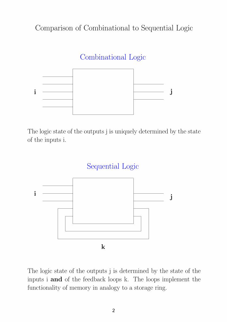
Comparison of Combinational to Sequential Logic
Combinational Logic
i j
The logic state of the outputs j is uniquely determined by the state
of the inputs i.
Sequential Logic
i j
k
The logic state of the outputs j is determined by the state of the
inputs i and of the feedback loops k. The loops implement the
functionality of memory in analogy to a storage ring.
2
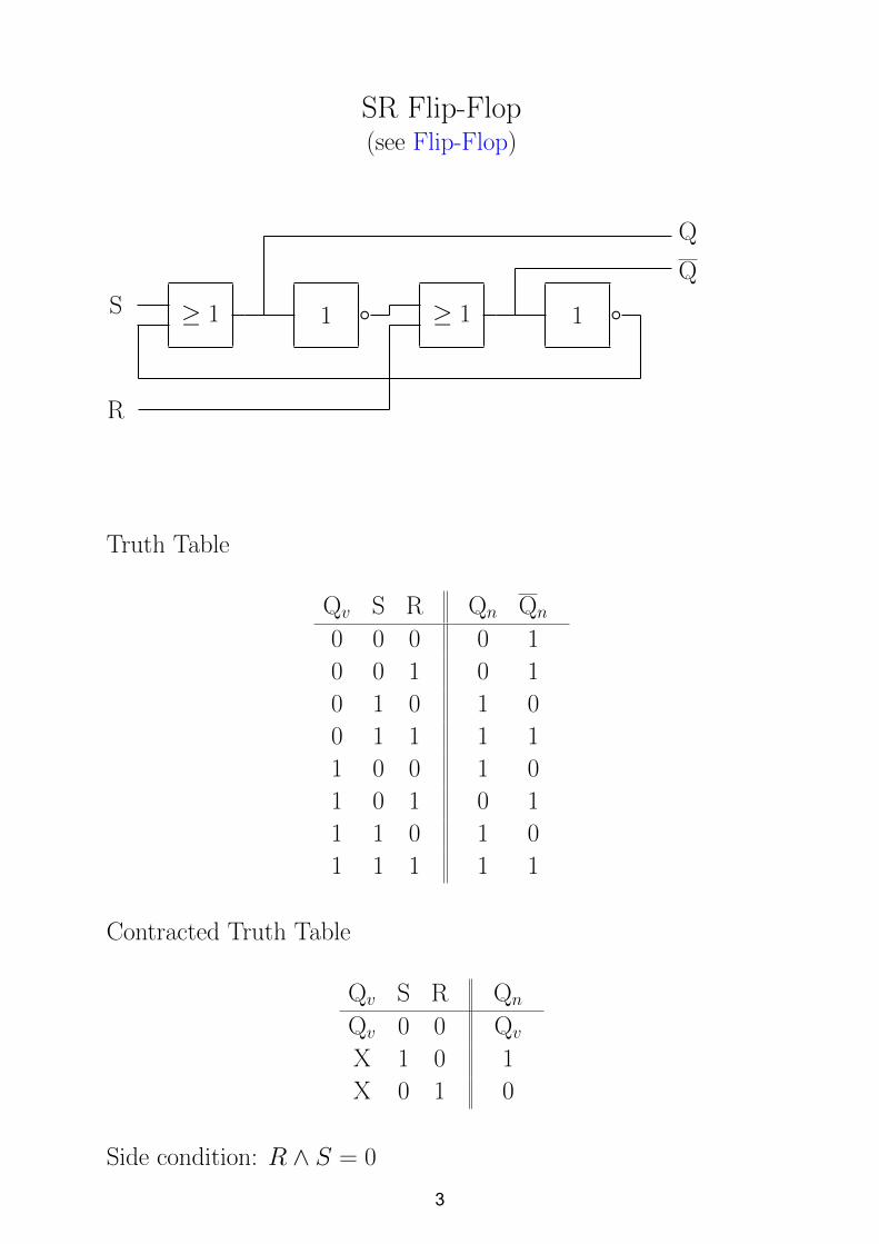
SR Flip-Flop(see Flip-Flop)
≥ 1 1 d ≥ 1 1 dS
R
Q
Q
Truth Table
Qv S R Qn Qn
0 0 0 0 1
0 0 1 0 1
0 1 0 1 0
0 1 1 1 1
1 0 0 1 0
1 0 1 0 1
1 1 0 1 0
1 1 1 1 1
Contracted Truth Table
Qv S R Qn
Qv 0 0 Qv
X 1 0 1
X 0 1 0
Side condition: R ∧ S = 0
3
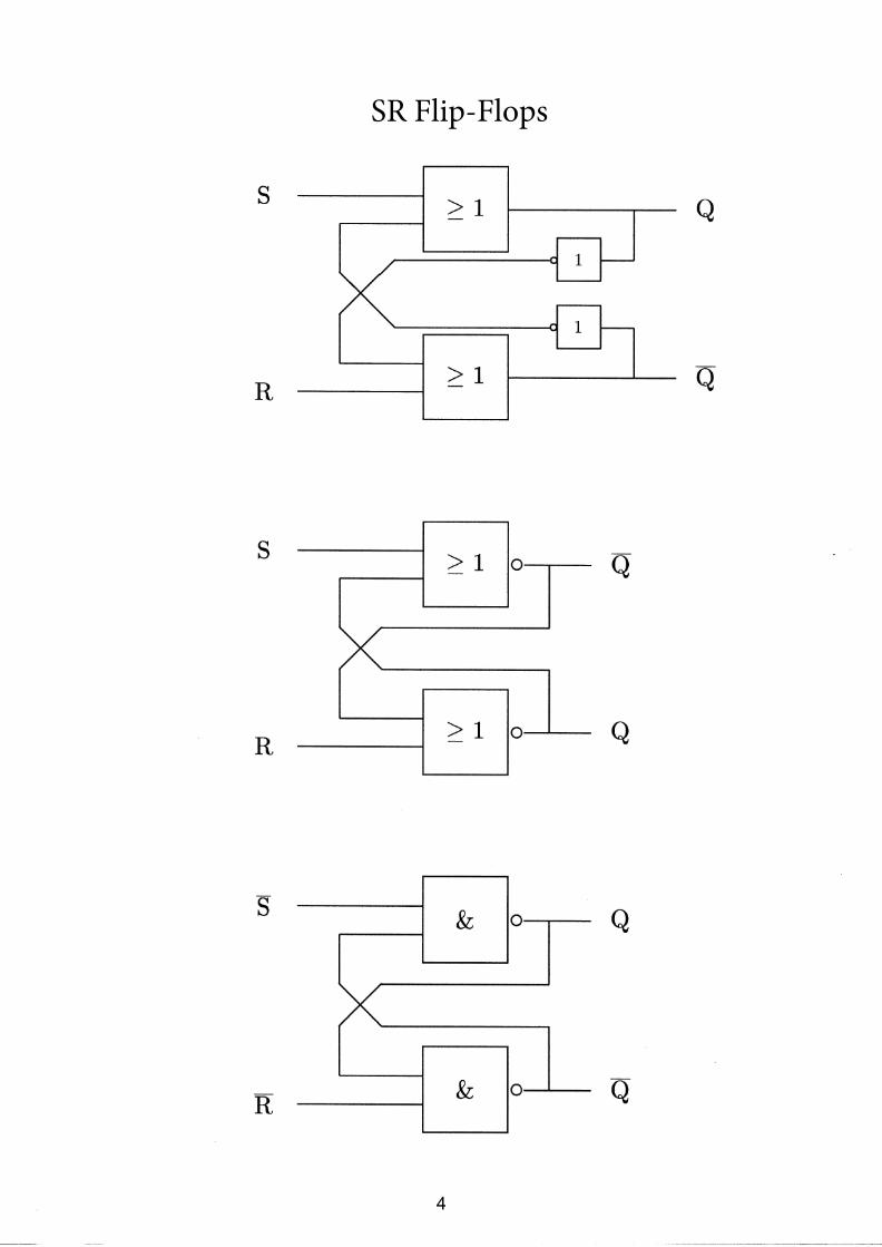
SR Flip-Flops
4
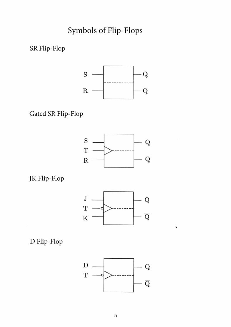
Symbols of Flip-Flops
SR Flip-Flop
Gated SR Flip-Flop
JK Flip-Flop
D Flip-Flop
5
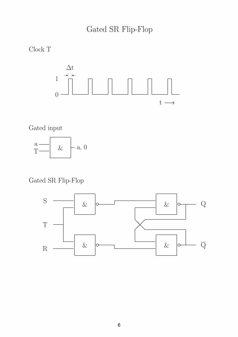
Gated SR Flip-Flop
Clock T
- �
∆t
t −→0
1
Gated input
&Ta
a, 0
Gated SR Flip-Flop
& e & e
& e & e
��� @@@
S
T
R
Q
Q
6
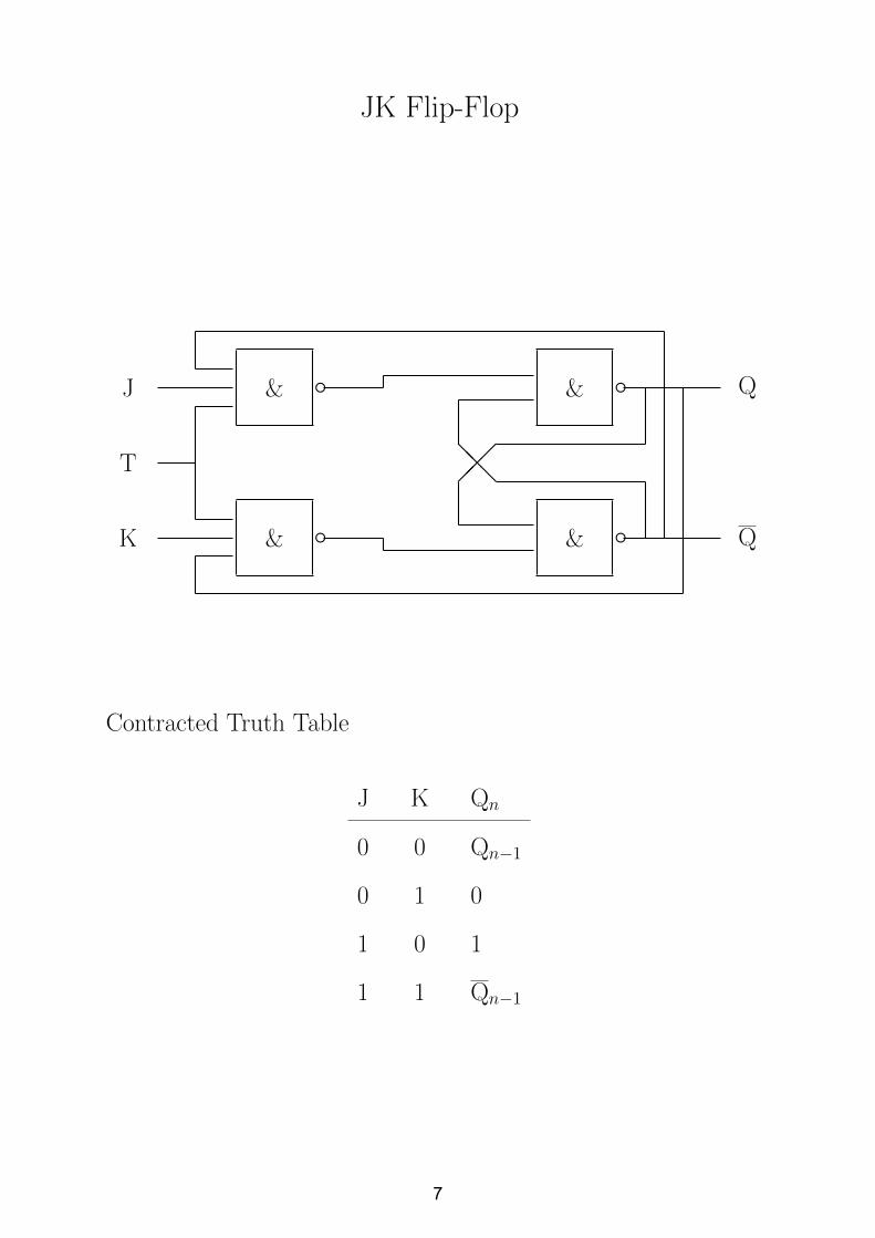
JK Flip-Flop
& e & e
& e & e
��� @@@
J
T
K
Q
Q
Contracted Truth Table
J K Qn
0 0 Qn−1
0 1 0
1 0 1
1 1 Qn−1
7
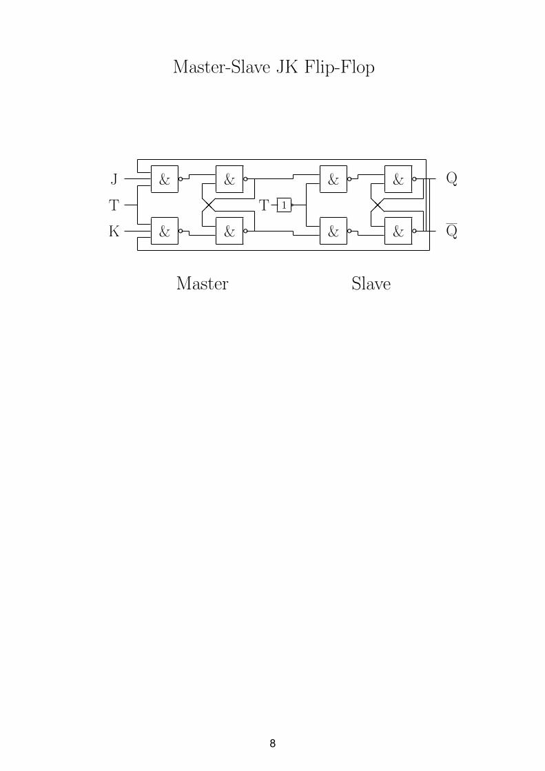
Master-Slave JK Flip-Flop
& c & c
& c & c��@@
J
T
K
Q
Q
T 1 a
Master Slave
& c & c
& c & c��@@
8
399
40
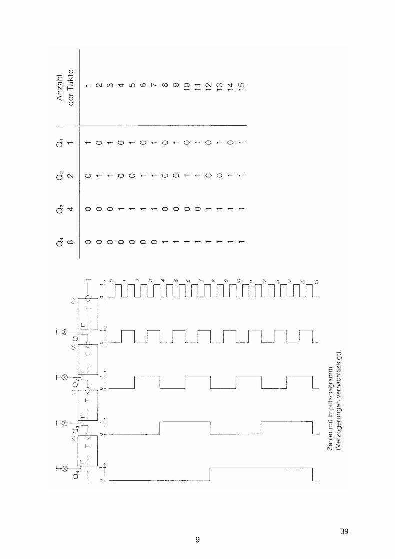
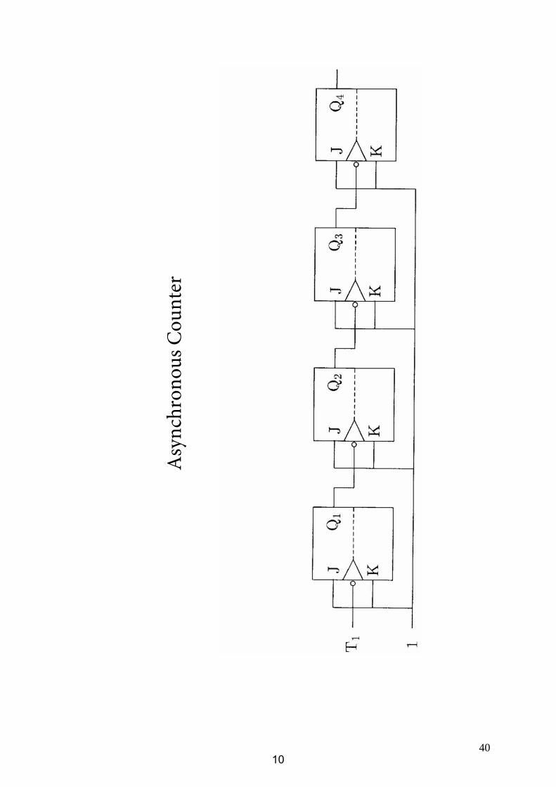
Asy
nchr
onou
s Cou
nter
10
41
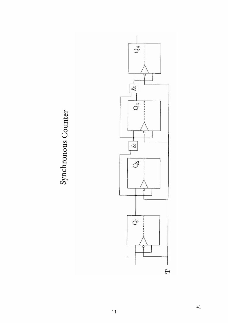
Sync
hron
ous C
ount
er
11

42
Sync
hron
ous D
ecad
e (B
CD
) Cou
nter
12
43
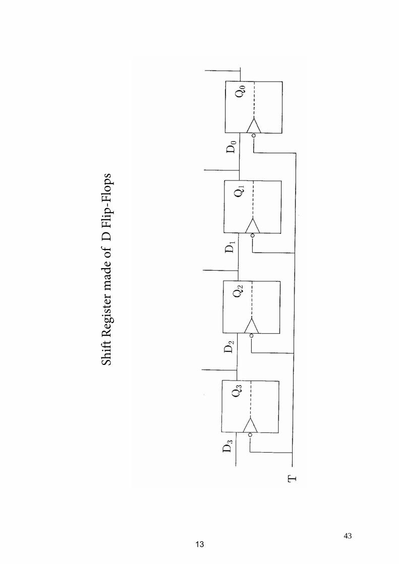
Shift
Reg
ister
mad
e of
D F
lip-F
lops
13

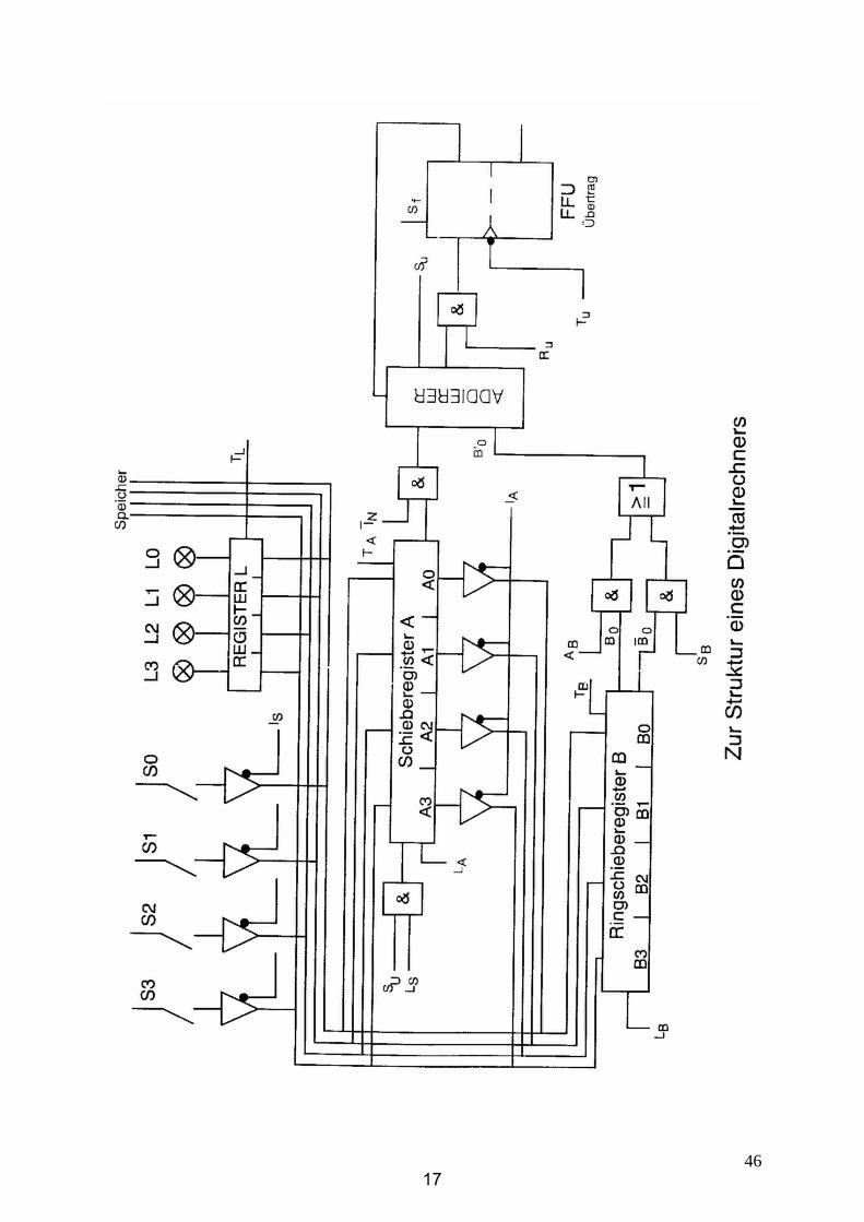
4. Computer Architecture and Functionality
4.1 Basic Components and Operations
4.1.1 Registers
4.1.2 Bus
4.1.3 Some Simple Operations
4.1.4 Control Unit
4.1.5 Memory
4.2 Basic Architectures
4.2.1 von Neumann Architecture
4.2.2 Memory-mapped IO
4.3 Examples of Microprocessors
4.3.1 Intel 4004
4.3.2 Rockwell 6502
4.3.3 ARM
4.4 Architectures: CISC and RISC
4.4.1 Comparison of CISC with RISC
4.4.2 Pipeline
4.4.3 Hazards: Issues in Pipeline Operation
4.4.4 Alpha 21x64
4.5 New Developments
4.5.1 EPIC
4.5.2 MPP employing GPUs
14
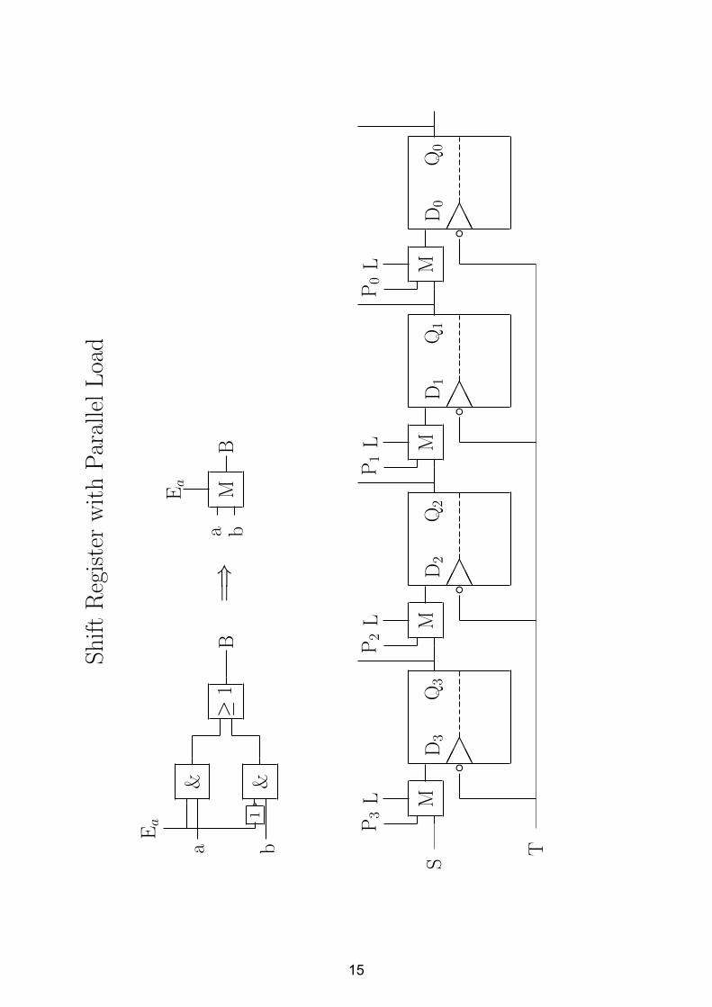
ShiftRegisterwithParallelLoad
MB
a b
Ea
=⇒
&&
1a
Ea
≥1
B
a b
dHHH � � �ML
Q3
D3
P3
dHHH � � �ML
Q2
D2
P2
dHHH � � �ML
Q1
D1
P1
dHHH � � �ML
Q0
D0
P0
T
S
15

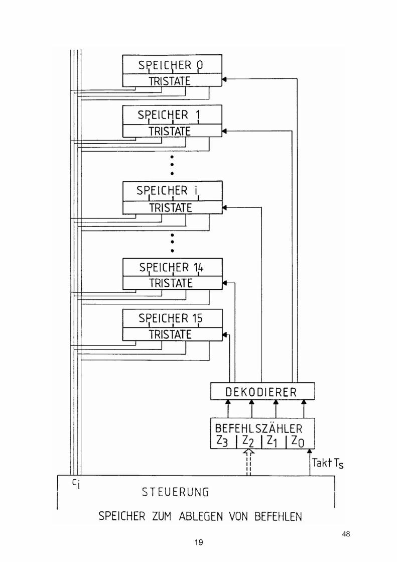
45
inou
t
TRIS
TATE
Buf
fer
16
4617
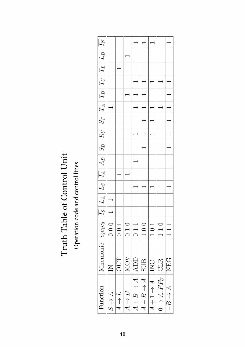
Trut
h Ta
ble
of C
ontr
ol U
nit
Ope
ratio
n co
de a
nd co
ntro
l lin
es
Func
tion
18
4819
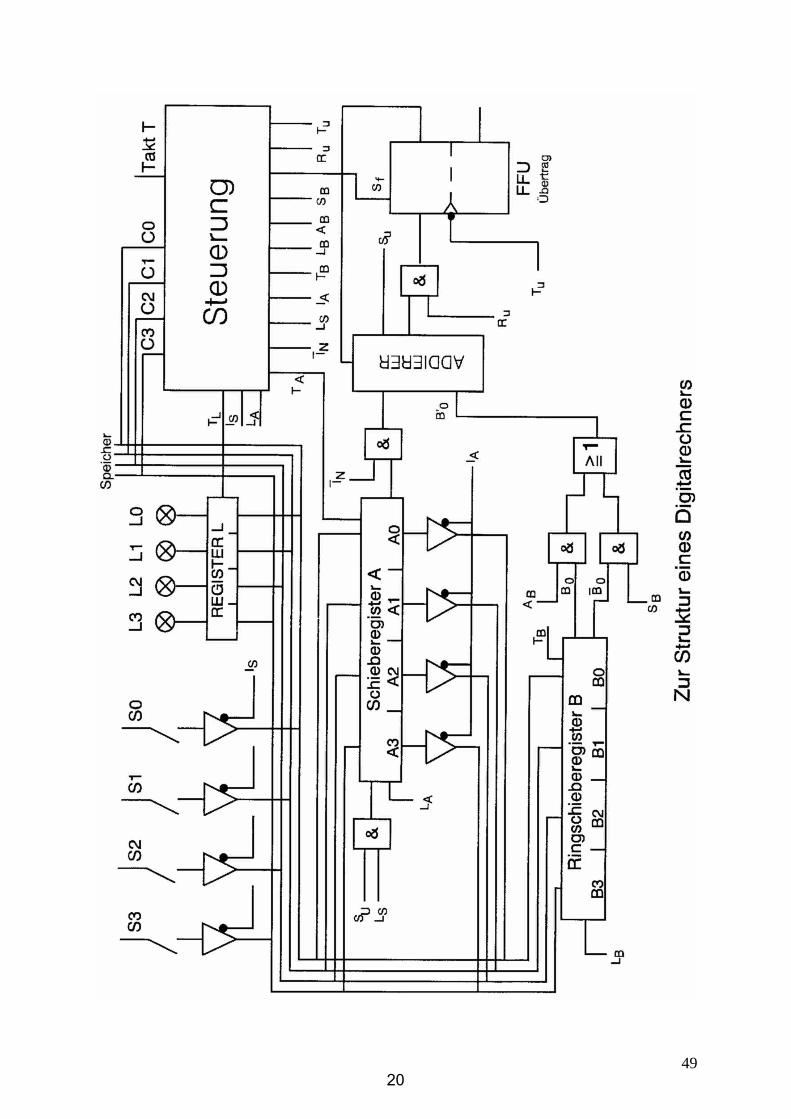
4920
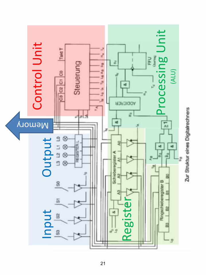
Inp
ut
O
utp
ut
Co
ntr
ol U
nit
P
roce
ssin
g U
nit
(
ALU
)
Reg
iste
r
Memory
21
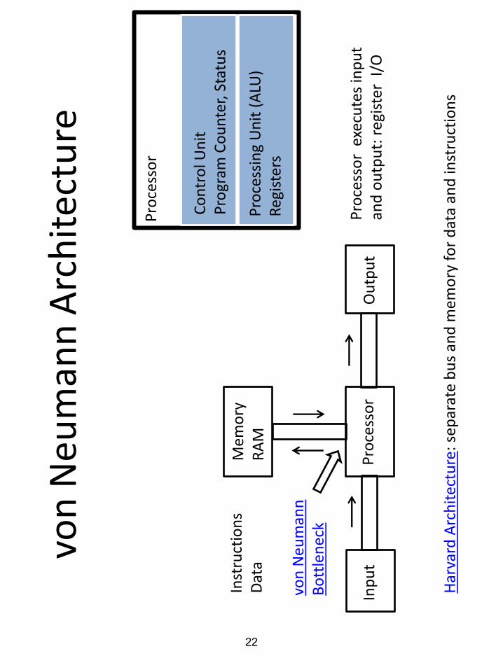
von
Neu
man
n A
rch
itec
ture
Mem
ory
R
AM
Inp
ut
Ou
tpu
t P
roce
sso
r
Pro
cess
or
Co
ntr
ol U
nit
P
rogr
am C
ou
nte
r, S
tatu
s
Pro
cess
ing
Un
it (
ALU
) R
egis
ters
Inst
ruct
ion
s D
ata
von
Ne
um
ann
B
ott
len
eck
Har
vard
Arc
hit
ectu
re:
sep
arat
e b
us
and
mem
ory
fo
r d
ata
and
inst
ruct
ion
s
Pro
cess
or
exe
cute
s in
pu
t an
d o
utp
ut:
reg
iste
r I/
O
22
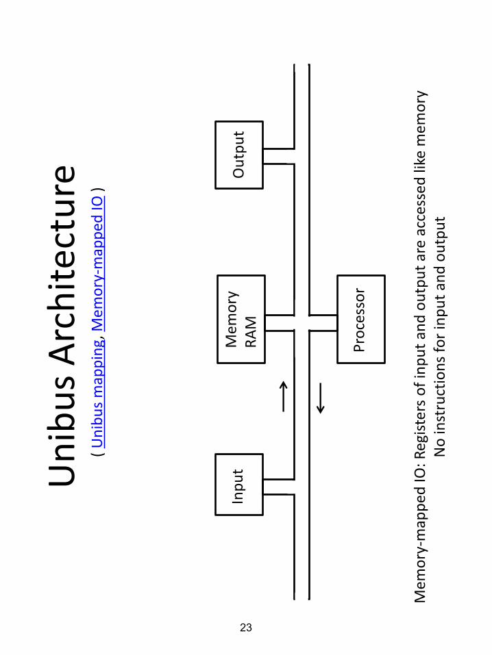
Un
ibu
s A
rch
itec
ture
Inp
ut
Ou
tpu
t
Pro
cess
or
Mem
ory
R
AM
Mem
ory
-map
pe
d IO
: Reg
iste
rs o
f in
pu
t an
d o
utp
ut
are
acc
esse
d li
ke m
emo
ry
N
o in
stru
ctio
ns
for
inp
ut
and
ou
tpu
t
( U
nib
us
map
pin
g, M
emo
ry-m
app
ed
IO )
23

5124
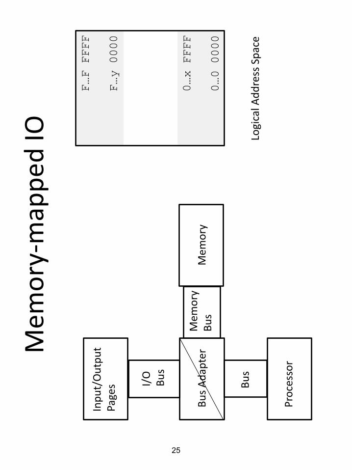
0…x FFFF
0…0 0000
F…F FFFF
F…y 0000
I/O
B
us
Mem
ory
Bu
s
Bu
s
Pro
cess
or
Bu
s A
dap
ter
Mem
ory
Inp
ut/
Ou
tpu
t Pa
ges
Logi
cal A
dd
ress
Sp
ace
Mem
ory
-map
pe
d IO
25
5226
5327
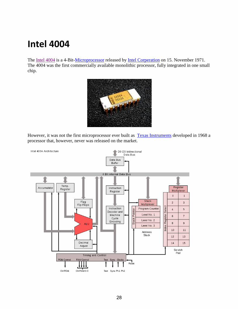
Intel 4004
The Intel 4004 is a 4-Bit-Microprocessor released by Intel Corperation on 15. November 1971.
The 4004 was the first commercially available monolithic processor, fully integrated in one small
chip.
However, it was not the first microprocessor ever built as Texas Instruments developed in 1968 a
processor that, however, never was released on the market.
28
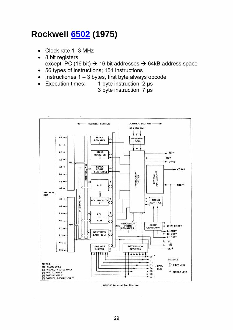
Rockwell 6502 (1975)
Clock rate 1- 3 MHz 8 bit registers
except PC (16 bit) 16 bit addresses 64kB address space 56 types of instructions; 151 instructions Instructiones 1 – 3 bytes, first byte always opcode Execution times: 1 byte instruction 2 µs
3 byte instruction 7 µs
29
30
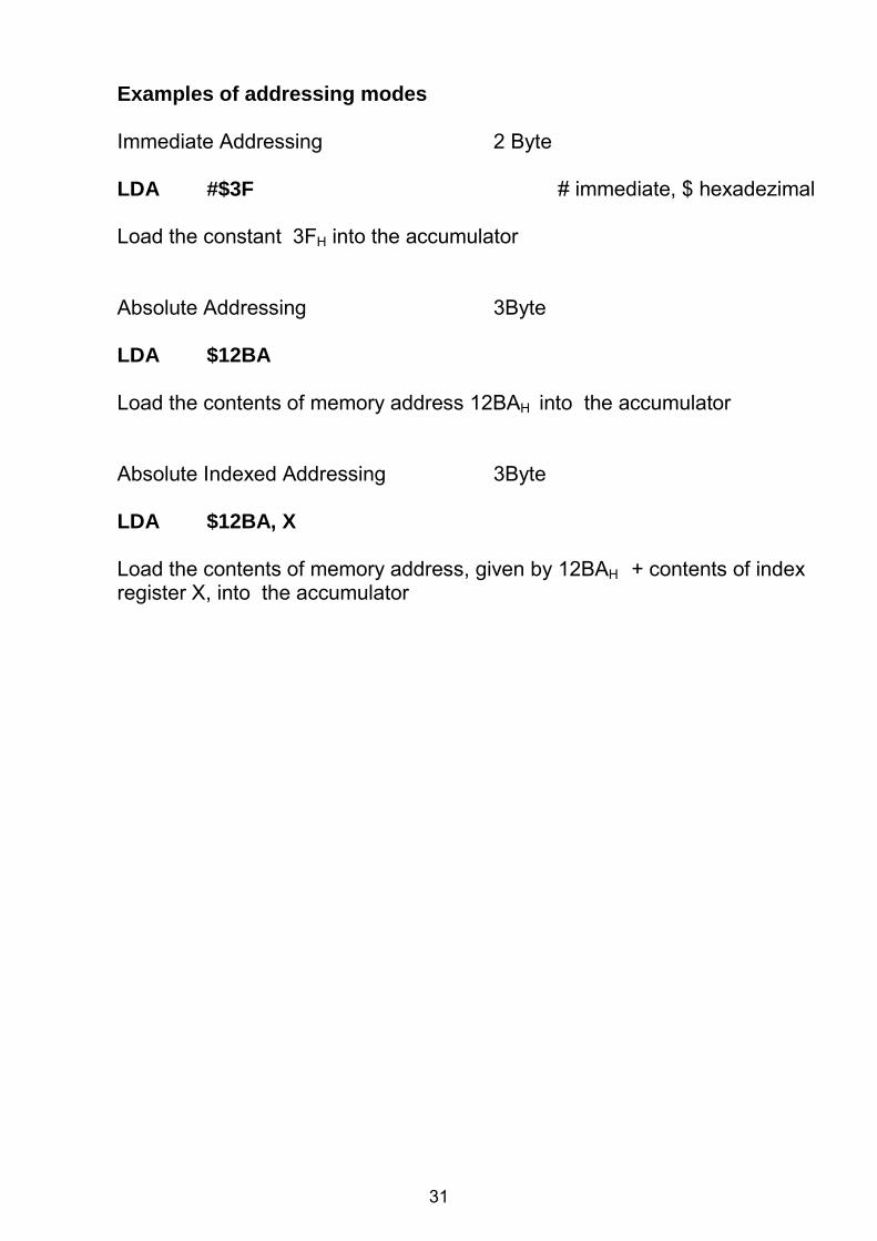
Examples of addressing modes Immediate Addressing 2 Byte LDA #$3F # immediate, $ hexadezimal Load the constant 3FH into the accumulator Absolute Addressing 3Byte LDA $12BA Load the contents of memory address 12BAH into the accumulator Absolute Indexed Addressing 3Byte LDA $12BA, X Load the contents of memory address, given by 12BAH + contents of index register X, into the accumulator
31
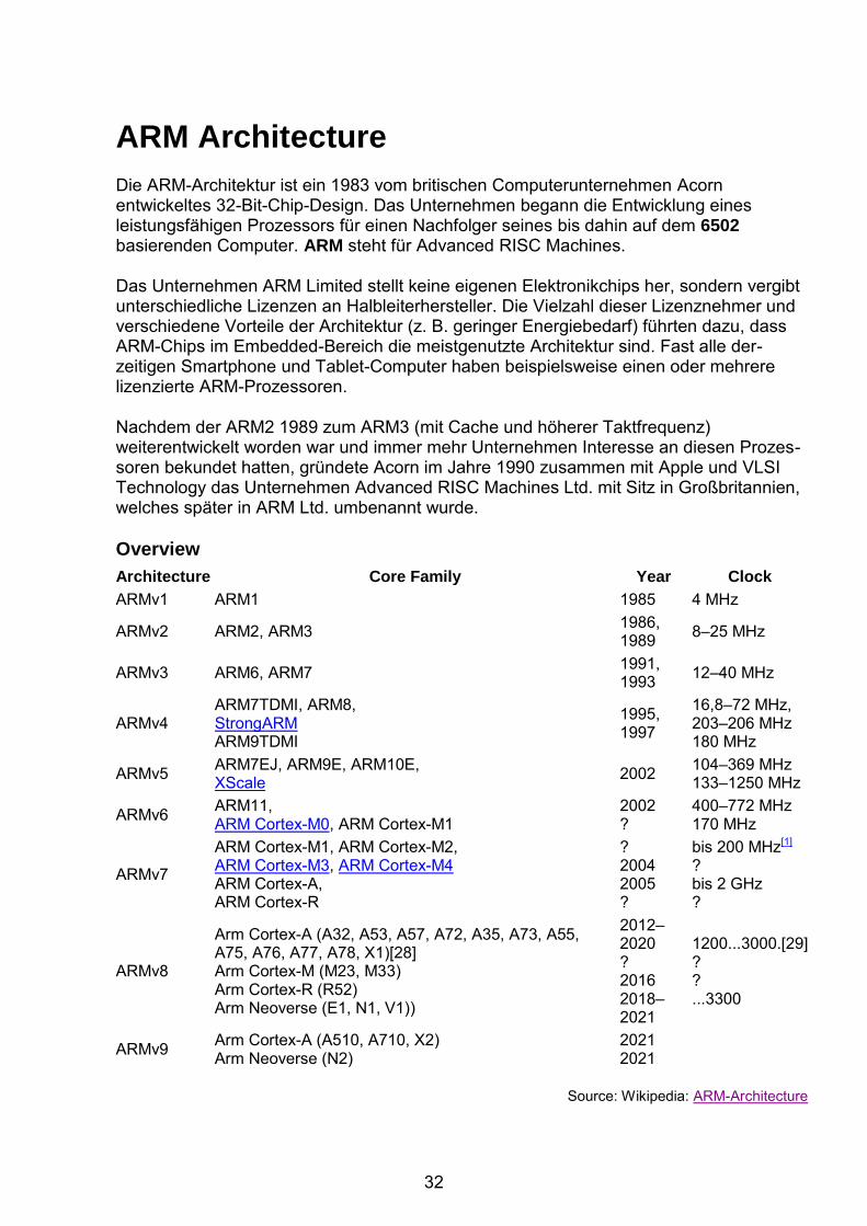
ARM Architecture
Die ARM-Architektur ist ein 1983 vom britischen Computerunternehmen Acorn entwickeltes 32-Bit-Chip-Design. Das Unternehmen begann die Entwicklung eines leistungsfähigen Prozessors für einen Nachfolger seines bis dahin auf dem 6502 basierenden Computer. ARM steht für Advanced RISC Machines.
Das Unternehmen ARM Limited stellt keine eigenen Elektronikchips her, sondern vergibt unterschiedliche Lizenzen an Halbleiterhersteller. Die Vielzahl dieser Lizenznehmer und verschiedene Vorteile der Architektur (z. B. geringer Energiebedarf) führten dazu, dass ARM-Chips im Embedded-Bereich die meistgenutzte Architektur sind. Fast alle der-zeitigen Smartphone und Tablet-Computer haben beispielsweise einen oder mehrere lizenzierte ARM-Prozessoren.
Nachdem der ARM2 1989 zum ARM3 (mit Cache und höherer Taktfrequenz) weiterentwickelt worden war und immer mehr Unternehmen Interesse an diesen Prozes-soren bekundet hatten, gründete Acorn im Jahre 1990 zusammen mit Apple und VLSI Technology das Unternehmen Advanced RISC Machines Ltd. mit Sitz in Großbritannien, welches später in ARM Ltd. umbenannt wurde.
Overview
Architecture Core Family Year Clock
ARMv1 ARM1 1985 4 MHz
ARMv2 ARM2, ARM3 1986, 1989 8–25 MHz
ARMv3 ARM6, ARM7 1991, 1993 12–40 MHz
ARMv4 ARM7TDMI, ARM8, StrongARM ARM9TDMI
1995, 1997
16,8–72 MHz, 203–206 MHz 180 MHz
ARMv5 ARM7EJ, ARM9E, ARM10E, XScale 2002 104–369 MHz
133–1250 MHz
ARMv6 ARM11, ARM Cortex-M0, ARM Cortex-M1
2002 ?
400–772 MHz 170 MHz
ARMv7 ARM Cortex-M1, ARM Cortex-M2, ARM Cortex-M3, ARM Cortex-M4 ARM Cortex-A, ARM Cortex-R
? 2004 2005 ?
bis 200 MHz[1] ? bis 2 GHz ?
ARMv8
Arm Cortex-A (A32, A53, A57, A72, A35, A73, A55, A75, A76, A77, A78, X1)[28] Arm Cortex-M (M23, M33) Arm Cortex-R (R52) Arm Neoverse (E1, N1, V1))
2012–2020 ? 2016 2018–2021
1200...3000.[29] ? ? ...3300
ARMv9 Arm Cortex-A (A510, A710, X2) Arm Neoverse (N2)
2021 2021
Source: Wikipedia: ARM-Architecture
32
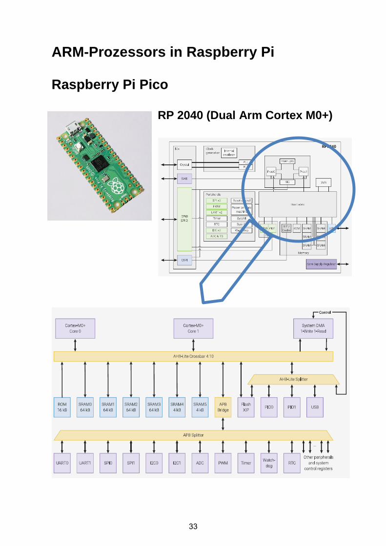
ARM-Prozessors in Raspberry Pi Raspberry Pi Pico
RP 2040 (Dual Arm Cortex M0+)
33
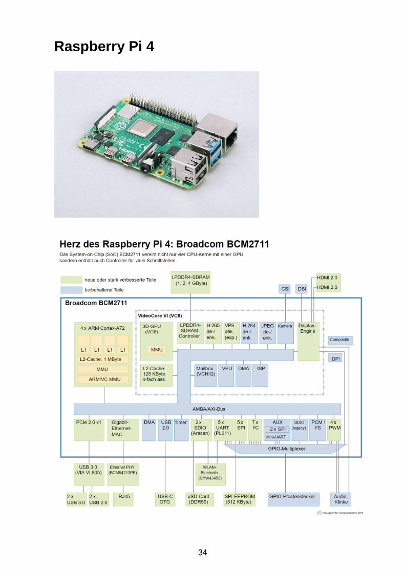
Raspberry Pi 4
34
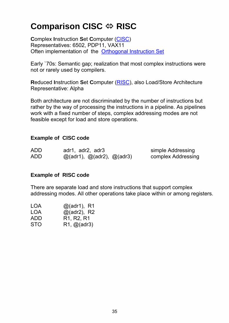
Comparison CISC RISC Complex Instruction Set Computer (CISC) Representatives: 6502, PDP11, VAX11 Often implementation of the Orthogonal Instruction Set Early `70s: Semantic gap; realization that most complex instructions were not or rarely used by compilers. Reduced Instruction Set Computer (RISC), also Load/Store Architecture Representative: Alpha Both architecture are not discriminated by the number of instructions but rather by the way of processing the instructions in a pipeline. As pipelines work with a fixed number of steps, complex addressing modes are not feasible except for load and store operations. Example of CISC code ADD adr1, adr2, adr3 simple Addressing ADD @(adr1), @(adr2), @(adr3) complex Addressing Example of RISC code There are separate load and store instructions that support complex addressing modes. All other operations take place within or among registers. LOA @(adr1), R1 LOA @(adr2), R2 ADD R1, R2, R1 STO R1, @(adr3)
35
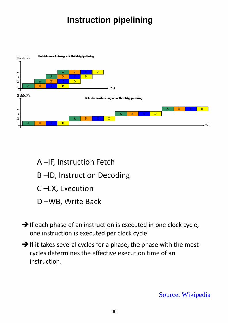
Instruction pipelining
A –IF, Instruction Fetch
B –ID, Instruction Decoding
C –EX, Execution
D –WB, Write Back
Source: Wikipedia
If each phase of an instruction is executed in one clock cycle, one instruction is executed per clock cycle.
If it takes several cycles for a phase, the phase with the most cycles determines the effective execution time of an instruction.
36
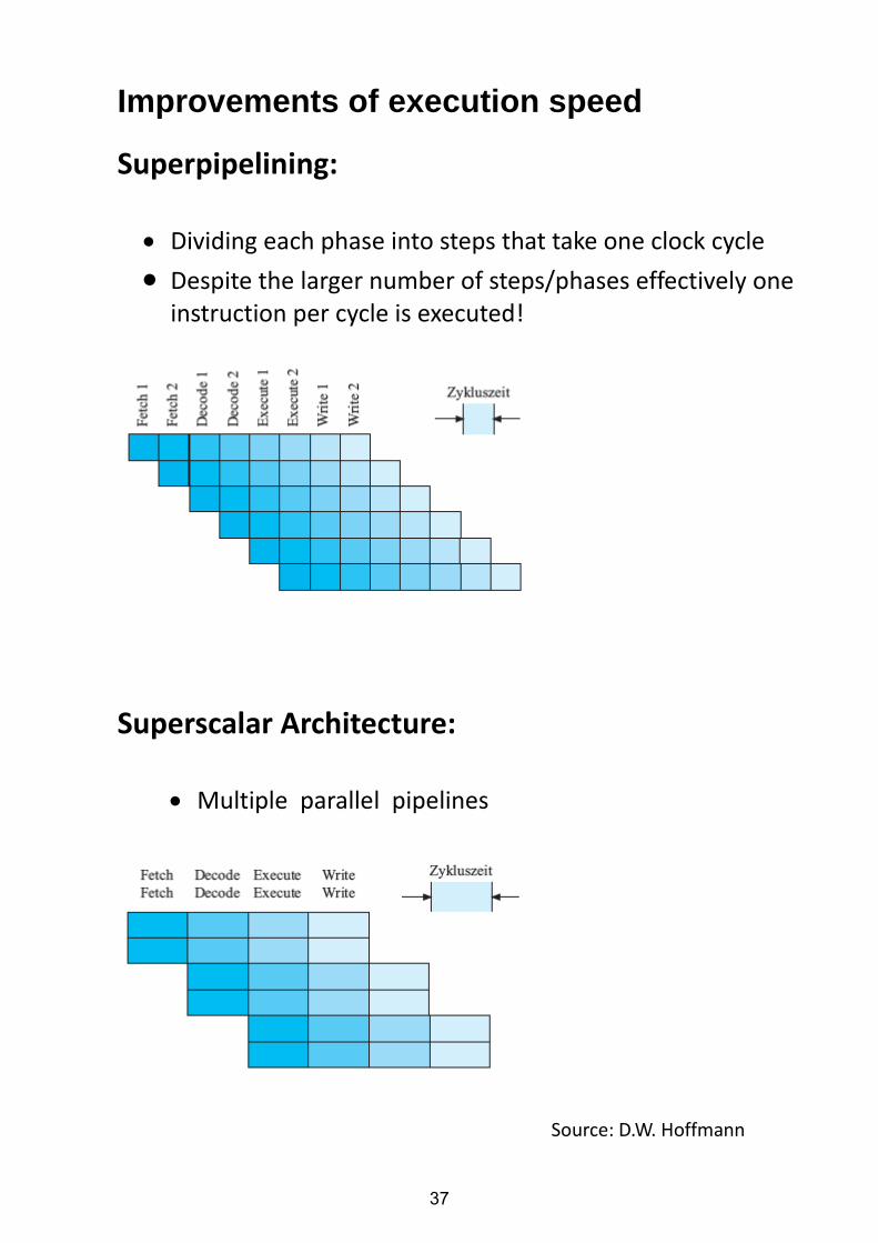
Improvements of execution speed
Superpipelining:
Dividing each phase into steps that take one clock cycle
Despite the larger number of steps/phases effectively one instruction per cycle is executed!
Superscalar Architecture:
Multiple parallel pipelines
Source: D.W. Hoffmann
37
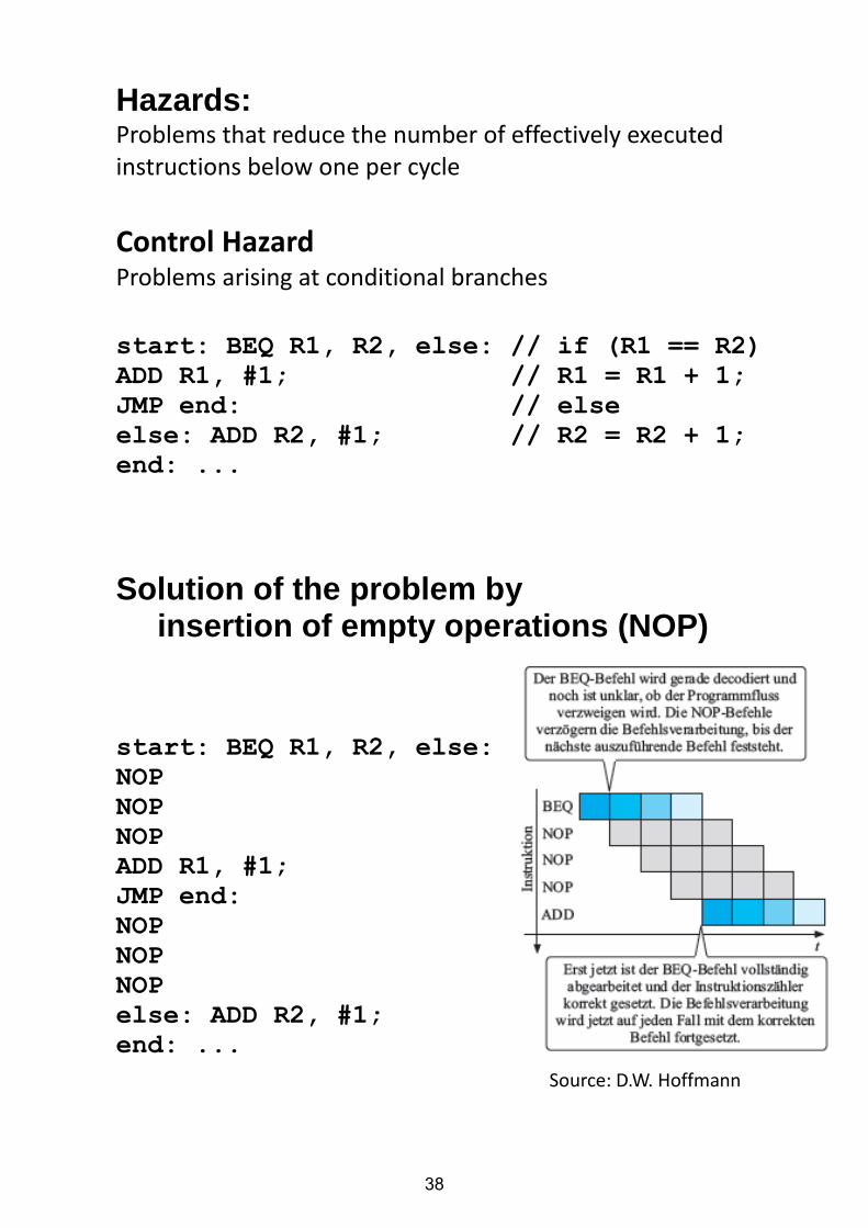
Hazards: Problems that reduce the number of effectively executed instructions below one per cycle
Control Hazard Problems arising at conditional branches
start: BEQ R1, R2, else: // if (R1 == R2)
ADD R1, #1; // R1 = R1 + 1;
JMP end: // else
else: ADD R2, #1; // R2 = R2 + 1;
end: ...
Solution of the problem by insertion of empty operations (NOP)
start: BEQ R1, R2, else:
NOP
NOP
NOP
ADD R1, #1;
JMP end:
NOP
NOP
NOP
else: ADD R2, #1;
end: ...
Source: D.W. Hoffmann
38
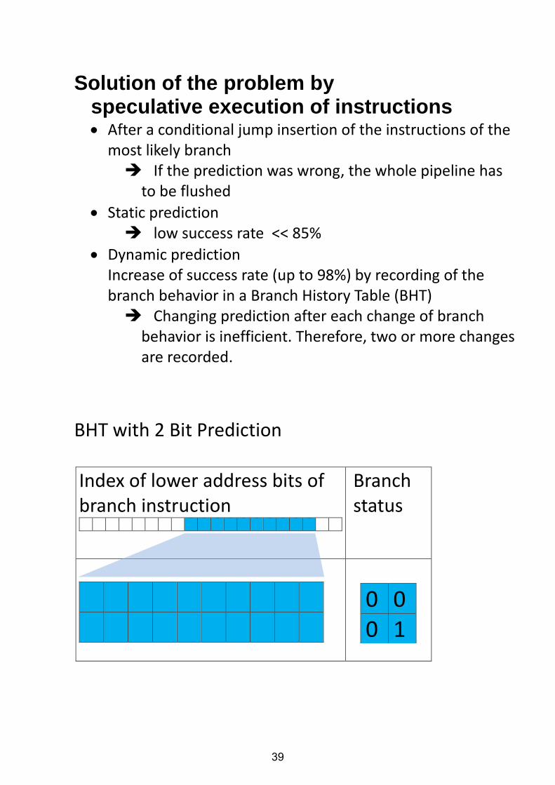
Solution of the problem by speculative execution of instructions After a conditional jump insertion of the instructions of the
most likely branch If the prediction was wrong, the whole pipeline has
to be flushed
Static prediction low success rate << 85%
Dynamic prediction Increase of success rate (up to 98%) by recording of the branch behavior in a Branch History Table (BHT) Changing prediction after each change of branch
behavior is inefficient. Therefore, two or more changes are recorded.
BHT with 2 Bit Prediction Index of lower address bits of branch instruction
Branch status
0 0 0 1
39
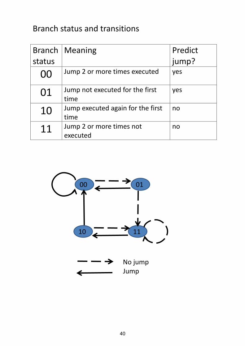
Branch status and transitions Branch status
Meaning Predict jump?
00 Jump 2 or more times executed
yes
01 Jump not executed for the first time
yes
10 Jump executed again for the first time
no
11 Jump 2 or more times not executed
no
01 00
10 11
Jump
No jump
40
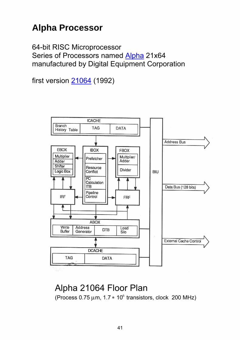
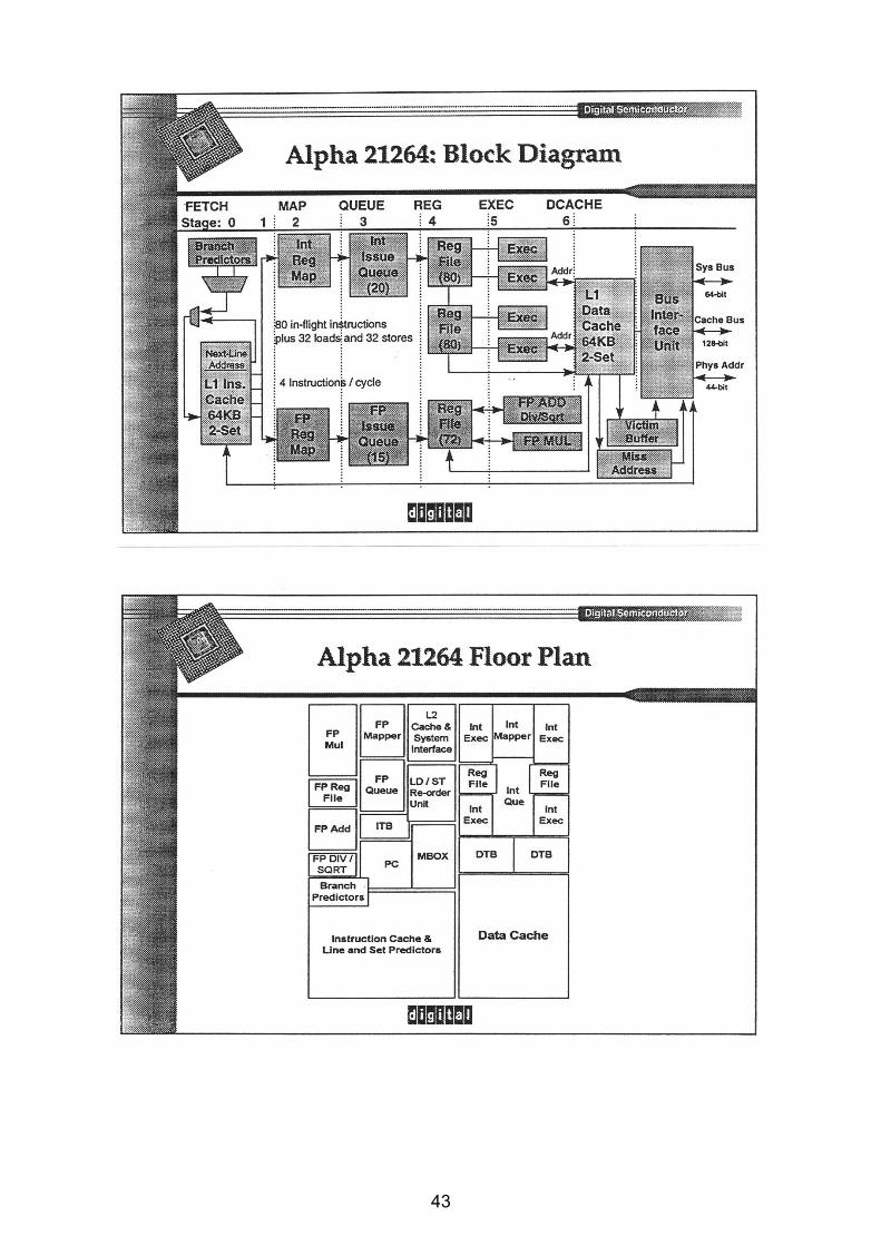
Alpha Processor 64-bit RISC Microprocessor Series of Processors named Alpha 21x64 manufactured by Digital Equipment Corporation first version 21064 (1992)
Alpha 21064 Floor Plan (Process 0.75 m, 1.710 transistors, clock 200 MHz)
41
Evolution of RISC Processors Example: Alpha 21064 21164 21264 … CMOS6 Technology: process 0.35 m, 6 layers
3 cm2 area 15.210 transistors
further increase of parallelization:
more pipelines 4 instructions per cycle superscalar 4 integer pipelines 2 floatingpoint pipelines
more efficient utilisation of pipelines more elaborate branch prediction out-of-order execution
initially, clock 500 MHz: 4 * 500 MHz 2000 MIPS later, clock 1250 MHz: 4 * 1250 MHz 5000 MIPS increase of speed by reduction of size: 0.35 m 0.25 m process
Problem: Enormous increase of logic required for distribution of instructions to pipelines, branch prediction, and out of order execution
42
43
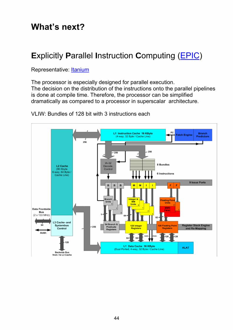
What’s next? Explicitly Parallel Instruction Computing (EPIC) Representative: Itanium The processor is especially designed for parallel execution. The decision on the distribution of the instructions onto the parallel pipelines is done at compile time. Therefore, the processor can be simplified dramatically as compared to a processor in superscalar architecture. VLIW: Bundles of 128 bit with 3 instructions each
44

Massively Parallel Processing (MPP) Usually implemented in vector processors Architecture is Single Instruction Multiple Data (SIMD) Example: adding two vectors A(i) and B(i) and storing the sum in C(i);
execution for each i // Kernel definition __global__ void VecAdd(float* A, float* B, float* C) { int i = threadIdx.x; C[i] = A[i] + B[i]; } int main() { ... // Kernel invocation with N threads VecAdd<<<1, N>>>(A, B, C); ... } Graphics processors (GPUs) typically execute vector operations to extremely wide vectors called streams Especially adapted GPUs (GPGPUs) are used for MPP in High Performance Computing Application in simulations and computations such as Computational Fluid Dynamics, Quantum Chemistry, Machine Vision and AI applications with Deep Learning
45
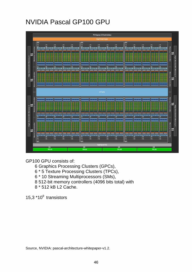
NVIDIA Pascal GP100 GPU
GP100 GPU consists of:
6 Graphics Processing Clusters (GPCs), 6 * 5 Texture Processing Clusters (TPCs), 6 * 10 Streaming Multiprocessors (SMs), 8 512-bit memory controllers (4096 bits total) with 8 * 512 kB L2 Cache.
15,3 *109 transistors Source, NVIDIA: pascal-architecture-whitepaper-v1.2.
46
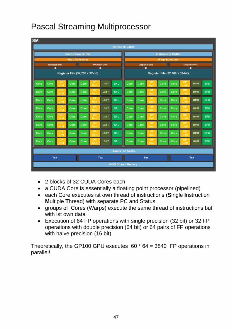
Pascal Streaming Multiprocessor
• 2 blocks of 32 CUDA Cores each • a CUDA Core is essentially a floating point processor (pipelined) • each Core executes ist own thread of instructions (Single Instruction
Multiple Thread) with separate PC and Status • groups of Cores (Warps) execute the same thread of instructions but
with ist own data • Execution of 64 FP operations with single precision (32 bit) or 32 FP
operations with double precision (64 bit) or 64 pairs of FP operations with halve precision (16 bit)
Theoretically, the GP100 GPU executes 60 * 64 = 3840 FP operations in parallel!
47
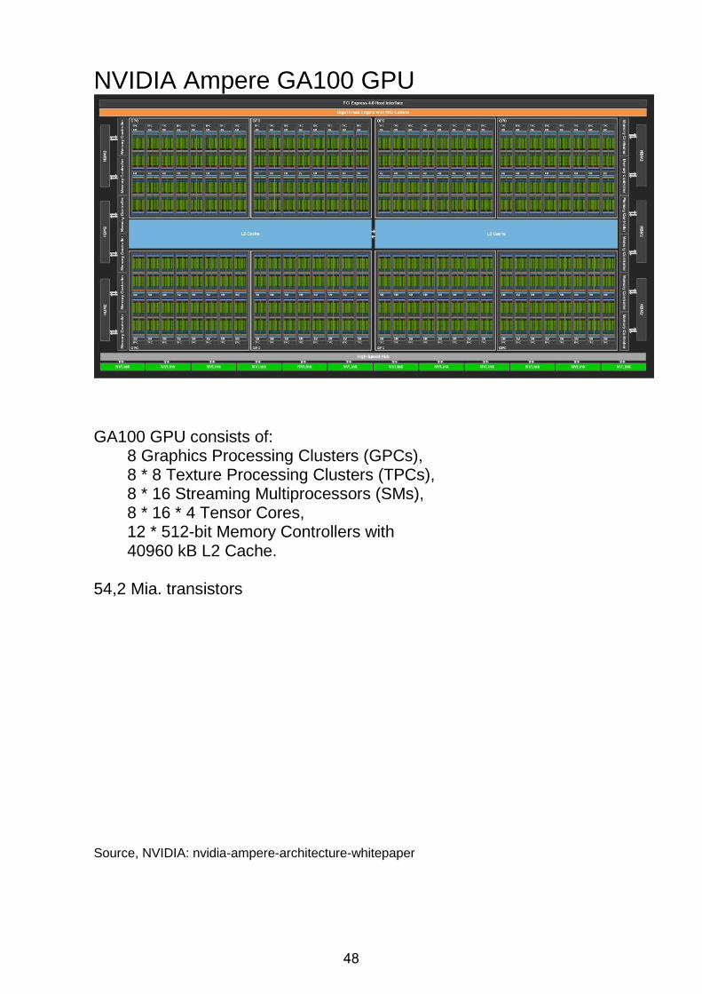
NVIDIA Ampere GA100 GPU
GA100 GPU consists of:
8 Graphics Processing Clusters (GPCs), 8 * 8 Texture Processing Clusters (TPCs), 8 * 16 Streaming Multiprocessors (SMs), 8 * 16 * 4 Tensor Cores, 12 * 512-bit Memory Controllers with 40960 kB L2 Cache.
54,2 Mia. transistors Source, NVIDIA: nvidia-ampere-architecture-whitepaper
48
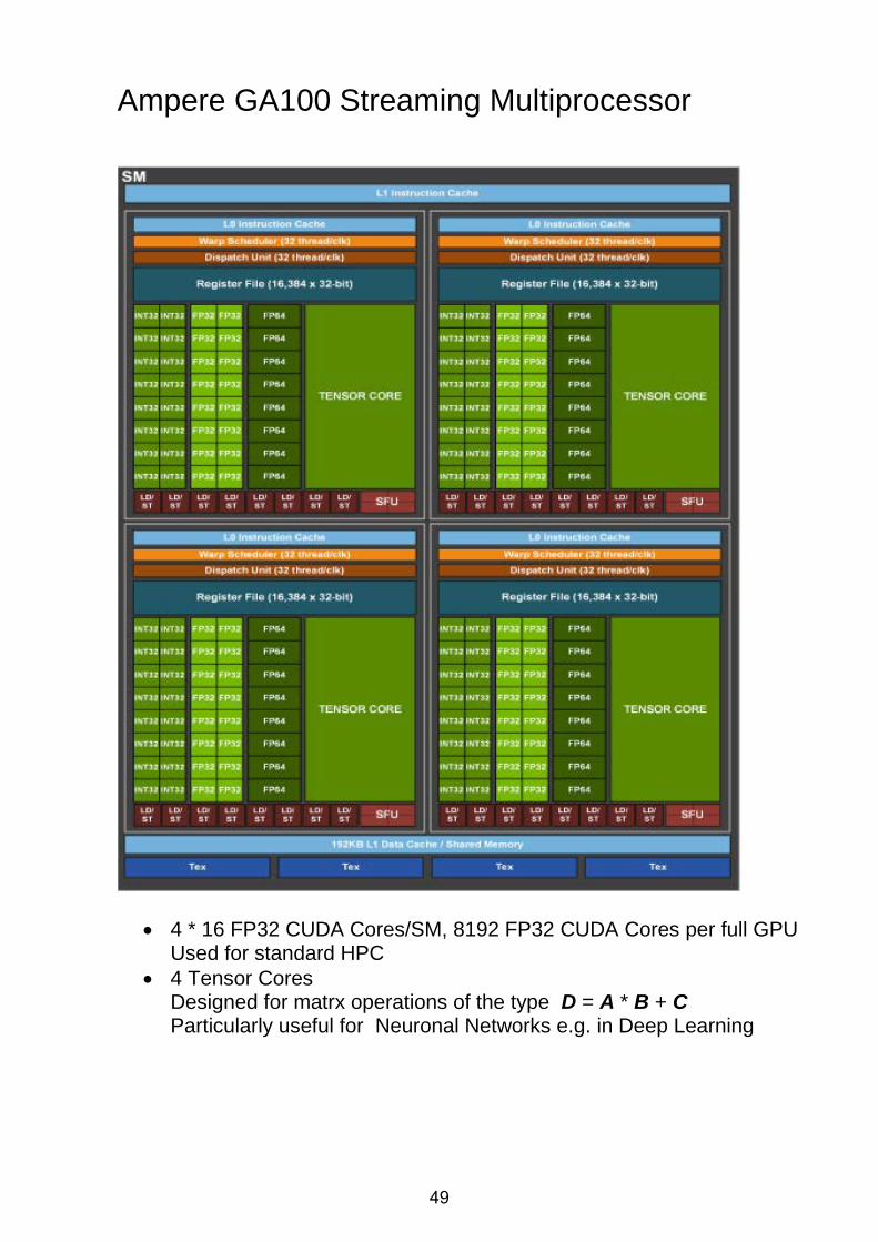
Ampere GA100 Streaming Multiprocessor
• 4 * 16 FP32 CUDA Cores/SM, 8192 FP32 CUDA Cores per full GPU Used for standard HPC
• 4 Tensor Cores Designed for matrx operations of the type D = A * B + C Particularly useful for Neuronal Networks e.g. in Deep Learning
49
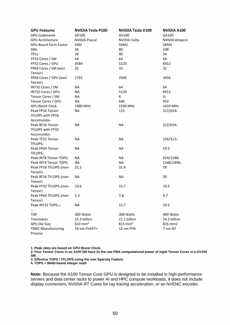
GPU Features NVIDIA Tesla P100 NVIDIA Tesla V100 NVIDIA A100 GPU Codename GP100 GV100 GA100 GPU Architecture NVIDIA Pascal NVIDIA Volta NVIDIA Ampere GPU Board Form Factor SXM SXM2 SXM4 SMs 56 80 108 TPCs 28 40 54 FP32 Cores / SM 64 64 64 FP32 Cores / GPU 3584 5120 6912 FP64 Cores / SM (excl. Tensor)
32 32 32
FP64 Cores / GPU (excl. Tensor)
1792 2560 3456
INT32 Cores / SM NA 64 64 INT32 Cores / GPU NA 5120 6912 Tensor Cores / SM NA 8 42
Tensor Cores / GPU NA 640 432 GPU Boost Clock 1480 MHz 1530 MHz 1410 MHz Peak FP16 Tensor TFLOPS with FP16 Accumulate1
NA 125 312/6243
Peak BF16 Tensor TFLOPS with FP32 Accumulate1
NA NA 312/6243
Peak TF32 Tensor TFLOPS1
NA NA 156/3123
Peak FP64 Tensor TFLOPS1
NA NA 19.5
Peak INT8 Tensor TOPS1 NA NA 624/12483 Peak INT4 Tensor TOPS1 NA NA 1248/24963
Peak FP16 TFLOPS1 (non-Tensor)
21.2 31.4 78
Peak BF16 TFLOPS1 (non-Tensor)
NA NA 39
Peak FP32 TFLOPS1 (non-Tensor)
10.6 15.7 19.5
Peak FP64 TFLOPS1 (non-Tensor)
5.3 7.8 9.7
Peak INT32 TOPS1,4 NA 15.7 19.5 … TDP 300 Watts 300 Watts 400 Watts Transistors 15.3 billion 21.1 billion 54.2 billion GPU Die Size 610 mm² 815 mm² 826 mm2 TSMC Manufacturing Process
16 nm FinFET+ 12 nm FFN 7 nm N7
1. Peak rates are based on GPU Boost Clock. 2. Four Tensor Cores in an A100 SM have 2x the raw FMA computational power of eight Tensor Cores in a GV100 SM. 3. Effective TOPS / TFLOPS using the new Sparsity Feature 4. TOPS = IMAD-based integer math
Note: Because the A100 Tensor Core GPU is designed to be installed in high-performance servers and data center racks to power AI and HPC compute workloads, it does not include display connectors, NVIDIA RT Cores for ray tracing acceleration, or an NVENC encoder.
50

Programming is done in a extended standard programming language Example C++: CUDA C Specific language elements control the paralleization Knowledge of the CUDA architecture is required
51