Embed Size (px)
Citation preview
ETSI EN 300 417-3-1 V1.2.1 (2001-10)
European Standard (Telecommunications series)
Transmission and Multiplexing (TM);Generic requirements of transport functionality of equipment;
Part 3-1: Synchronous Transport Module-N (STM-N)regenerator and multiplex section layer functions
ETSI
ETSI EN 300 417-3-1 V1.2.1 (2001-10)2
Reference REN/TM-01042-3-1
Keywords transmission, SDH, interface, architecture
ETSI
650 Route des Lucioles F-06921 Sophia Antipolis Cedex - FRANCE
Tel.: +33 4 92 94 42 00 Fax: +33 4 93 65 47 16
Siret N° 348 623 562 00017 - NAF 742 C
Association à but non lucratif enregistrée à la Sous-Préfecture de Grasse (06) N° 7803/88
Important notice
Individual copies of the present document can be downloaded from: http://www.etsi.org
The present document may be made available in more than one electronic version or in print. In any case of existing or perceived difference in contents between such versions, the reference version is the Portable Document Format (PDF).
In case of dispute, the reference shall be the printing on ETSI printers of the PDF version kept on a specific network drive within ETSI Secretariat.
Users of the present document should be aware that the document may be subject to revision or change of status. Information on the current status of this and other ETSI documents is available at
http://portal.etsi.org/tb/status/status.asp
If you find errors in the present document, send your comment to: [email protected]
Copyright Notification
No part may be reproduced except as authorized by written permission. The copyright and the foregoing restriction extend to reproduction in all media.
© European Telecommunications Standards Institute 2001.
All rights reserved.
ETSI
ETSI EN 300 417-3-1 V1.2.1 (2001-10)3
Contents
Intellectual Property Rights ................................................................................................................................9
Foreword.............................................................................................................................................................9
1 Scope ......................................................................................................................................................11
2 References ..............................................................................................................................................11
3 Definitions, abbreviations and symbols .................................................................................................11 3.1 Definitions........................................................................................................................................................11 3.2 Abbreviations ...................................................................................................................................................11 3.3 Symbols and Diagrammatic Conventions ........................................................................................................14 3.4 Introduction ......................................................................................................................................................14
4 STM-1 Regenerator Section Layer Functions........................................................................................14 4.1 STM-1 Regenerator Section Connection functions ..........................................................................................15 4.2 STM-1 Regenerator Section Trail Termination functions ................................................................................16 4.2.1 STM-1 Regenerator Section Trail Termination Source RS1_TT_So .........................................................16 4.2.2 STM-1 Regenerator Section Trail Termination Sink RS1_TT_Sk.............................................................17 4.3 STM-1 Regenerator Section Adaptation functions...........................................................................................19 4.3.1 STM-1 Regenerator Section to Multiplex Section Adaptation Source RS1/MS1_A_So ...........................19 4.3.2 STM-1 Regenerator Section to Multiplex Section Adaptation Sink RS1/MS1_A_Sk ...............................20 4.3.3 STM-1 Regenerator Section to DCC Adaptation Source RS1/DCC_A_So ...............................................21 4.3.4 STM-1 Regenerator Section to DCC Adaptation Sink RS1/DCC_A_Sk ...................................................22 4.3.5 STM-1 Regenerator Section to P0s Adaptation Source RS1/P0s_A_So/N ................................................22 4.3.6 STM-1 Regenerator Section to P0s Adaptation Sink RS1/P0s_A_Sk/N ....................................................23 4.3.7 STM-1 Regenerator Section toV0x Adaptation Source RS1/V0x_A_So ...................................................24 4.3.8 STM-1 Regenerator Section to V0x Adaptation Sink RS1/V0x_A_Sk......................................................25
5 STM-1 Multiplex Section Layer Functions............................................................................................26 5.1 STM-1 Multiplex Section Connection functions..............................................................................................28 5.2 STM-1 Multiplex Section Trail Termination functions....................................................................................28 5.2.1 STM-1 Multiplex Section Trail Termination Source MS1_TT_So ............................................................28 5.2.2 STM-1 Multiplex Section Trail Termination Sink MS1_TT_Sk................................................................29 5.3 STM-1 Multiplex Section Adaptation functions ..............................................................................................32 5.3.1 STM-1 Multiplex Section to S4 Layer Adaptation Source MS1/S4_A_So ................................................32 5.3.2 STM-1 Multiplex Section to S4 Layer Adaptation Sink MS1/S4_A_Sk....................................................34 5.3.3 STM-1 Multiplex Section to DCC Adaptation Source MS1/DCC_A_So ..................................................35 5.3.4 STM-1 Multiplex Section to DCC Adaptation Sink MS1/DCC_A_Sk ......................................................36 5.3.5 STM-1 Multiplex Section to P0s Adaptation Source MS1/P0s_A_So .......................................................36 5.3.6 STM-1 Multiplex Section to P0s Adaptation Sink MS1/P0s_A_Sk...........................................................37 5.3.7 STM-1 Multiplex Section to Synchronization Distribution Adaptation Source MS1/SD_A_So ...............38 5.3.8 STM-1 Multiplex Section to Synchronization Distribution Adaptation Sink MS1/SD_A_Sk ...................38 5.3.9 STM-1 Multiplex Section Layer Clock Adaptation Source MS1-LC_A_So..............................................38 5.4 STM-1 Multiplex Section Layer Monitoring Functions...................................................................................38 5.5 STM-1 Multiplex Section Linear Trail Protection Functions...........................................................................39 5.5.1 STM-1 Multiplex Section Linear Trail Protection Connection Functions..................................................39 5.5.1.1 STM-1 Multiplex Section 1+1 Linear Trail Protection Connection MS1P1+1_C................................39 5.5.1.2 STM-1 Multiplex Section 1:n Linear Trail Protection Connection MS1P1:n_C ..................................40 5.5.2 STM-1 Multiplex Section Linear Trail Protection Trail Termination Functions........................................42 5.5.2.1 Multiplex Section Protection Trail Termination Source MS1P_TT_So ...............................................42 5.5.2.2 Multiplex Section Protection Trail Termination Sink MS1P_TT_Sk ...................................................43 5.5.3 STM-1 Multiplex Section Linear Trail Protection Adaptation Functions...................................................44 5.5.3.1 STM-1 Multiplex Section to STM-1 Multiplex Section Protection Layer Adaptation Source
MS1/MS1P_A_So.................................................................................................................................44 5.5.3.2 STM-1 Multiplex Section to STM-1 Multiplex Section Protection Layer Adaptation Sink
MS1/MS1P_A_Sk.................................................................................................................................45
6 STM-4 Regenerator Section Layer Functions........................................................................................46 6.1 STM-4 Regenerator Section Connection functions ..........................................................................................47
ETSI
ETSI EN 300 417-3-1 V1.2.1 (2001-10)4
6.2 STM-4 Regenerator Section Trail Termination functions ................................................................................47 6.2.1 STM-4 Regenerator Section Trail Termination Source RS4_TT_So .........................................................47 6.2.2 STM-4 Regenerator Section Trail Termination Sink RS4_TT_Sk.............................................................49 6.3 STM-4 Regenerator Section Adaptation functions...........................................................................................51 6.3.1 STM-4 Regenerator Section to Multiplex Section Adaptation Source RS4/MS4_A_So ...........................51 6.3.2 STM-4 Regenerator Section to Multiplex Section Adaptation Sink RS4/MS4_A_Sk ...............................52 6.3.3 STM-4 Regenerator Section to DCC Adaptation Source RS4/DCC_A_So ...............................................53 6.3.4 STM-4 Regenerator Section to DCC Adaptation Sink RS4/DCC_A_Sk ...................................................53 6.3.5 STM-4 Regenerator Section to P0s Adaptation Source RS4/P0s_A_So/N ................................................54 6.3.6 STM-4 Regenerator Section to P0s Adaptation Sink RS4/P0s_A_Sk/N ....................................................55 6.3.7 STM-4 Regenerator Section to V0x Adaptation Source RS4/V0x_A_So ..................................................56 6.3.8 STM-4 Regenerator Section to V0x Adaptation Sink RS4/V0x_A_Sk......................................................57
7 STM-4 Multiplex Section Layer Functions............................................................................................58 7.1 STM-4 Multiplex Section Connection functions..............................................................................................60 7.2 STM-4 Multiplex Section Trail Termination functions....................................................................................61 7.2.1 STM-4 Multiplex Section Trail Termination Source MS4_TT_So ............................................................61 7.2.2 STM-4 Multiplex Section Trail Termination Sink MS4_TT_Sk................................................................62 7.3 STM-4 Multiplex Section Adaptation functions ..............................................................................................64 7.3.1 STM-4 Multiplex Section to S4 Layer Adaptation Source MS4/S4_A_So/(B,0).......................................64 7.3.2 STM-4 Multiplex Section to S4 Layer Adaptation Sink MS4/S4_A_Sk/(B,0) ..........................................67 7.3.3 STM-4 Multiplex Section to S4-4c Layer Adaptation Source MS4/S4-4c_A_So......................................68 7.3.4 STM-4 Multiplex Section to S4-4c Layer Adaptation Sink MS4/S4-4c_A_Sk..........................................70 7.3.5 STM-4 Multiplex Section to DCC Adaptation Source MS4/DCC_A_So ..................................................72 7.3.6 STM-4 Multiplex Section to DCC Adaptation Sink MS4/DCC_A_Sk ......................................................72 7.3.7 STM-4 Multiplex Section to P0s Adaptation Source MS4/P0s_A_So .......................................................73 7.3.8 STM-4 Multiplex Section to P0s Adaptation Sink MS4/P0s_A_Sk...........................................................74 7.3.9 STM-4 Multiplex Section to Synchronization Distribution Adaptation Source MS4/SD_A_So ...............75 7.3.10 STM-4 Multiplex Section to Synchronization Distribution Adaptation Sink MS4/SD_A_Sk ...................75 7.3.11 STM-4 Multiplex Section Layer Clock Adaptation Source MS4-LC_A_So..............................................75 7.4 STM-4 Multiplex Section Layer Monitoring Functions...................................................................................75 7.5 STM-4 Multiplex Section Linear Trail Protection Functions...........................................................................75 7.5.1 STM-4 Multiplex Section Linear Trail Protection Connection Functions..................................................75 7.5.1.1 STM-4 Multiplex Section 1+1 Linear Trail Protection Connection MS4P1+1_C................................75 7.5.1.2 STM-4 Multiplex Section 1:n Linear Trail Protection Connection MS4P1:n_C ..................................77 7.5.2 STM-4 Multiplex Section Linear Trail Protection Trail Termination Functions........................................78 7.5.2.1 Multiplex Section Protection Trail Termination Source MS4P_TT_So ...............................................78 7.5.2.2 Multiplex Section Protection Trail Termination Sink MS4P_TT_Sk ...................................................79 7.5.3 STM-4 Multiplex Section Linear Trail Protection Adaptation Functions...................................................80 7.5.3.1 STM-4 Multiplex Section to STM-4 Multiplex Section Protection Layer Adaptation Source
MS4/MS4P_A_So.................................................................................................................................80 7.5.3.2 STM-4 Multiplex Section to STM-4 Multiplex Section Protection Layer Adaptation Sink
MS4/MS4P_A_Sk.................................................................................................................................81
8 STM-16 Regenerator Section Layer Functions......................................................................................82 8.1 STM-16 Regenerator Section Connection functions ........................................................................................83 8.2 STM-16 Regenerator Section Trail Termination functions ..............................................................................83 8.2.1 STM-16 Regenerator Section Trail Termination Source RS16_TT_So .....................................................83 8.2.2 STM-16 Regenerator Section Trail Termination Sink RS16_TT_Sk .........................................................85 8.3 STM-16 Regenerator Section Adaptation functions.........................................................................................87 8.3.1 STM-16 Regenerator Section to Multiplex Section Adaptation Source RS16/MS16_A_So......................87 8.3.2 STM-16 Regenerator Section to Multiplex Section Adaptation Sink RS16/MS16_A_Sk .........................88 8.3.3 STM-16 Regenerator Section to DCC Adaptation Source RS16/DCC_A_So ...........................................88 8.3.4 STM-16 Regenerator Section to DCC Adaptation Sink RS16/DCC_A_Sk ...............................................89 8.3.5 STM-16 Regenerator Section to P0s Adaptation Source RS16/P0s_A_So/N ............................................90 8.3.6 STM-16 Regenerator Section to P0s Adaptation Sink RS16/P0s_A_Sk/N ................................................91 8.3.7 STM-16 Regenerator Section to V0x Adaptation Source RS16/V0x_A_So ..............................................92 8.3.8 STM-16 Regenerator Section to V0x Adaptation Sink RS16/V0x_A_Sk..................................................92
9 STM-16 Multiplex Section Layer Functions..........................................................................................93 9.1 STM-16 Multiplex Section Connection functions............................................................................................98 9.2 STM-16 Multiplex Section Trail Termination functions..................................................................................98 9.2.1 STM-16 Multiplex Section Trail Termination Source MS16_TT_So ........................................................98
ETSI
ETSI EN 300 417-3-1 V1.2.1 (2001-10)5
9.2.2 STM-16 Multiplex Section Trail Termination Sink MS16_TT_Sk............................................................99 9.3 STM-16 Multiplex Section Adaptation functions ..........................................................................................101 9.3.1 STM-16 Multiplex Section to S4 Layer Adaptation Source MS16/S4_A_So/(C,B,0) .............................101 9.3.2 STM-16 Multiplex Section to S4 Layer Adaptation Sink MS16/S4_A_Sk/(C,B,0).................................103 9.3.3 STM-16 Multiplex Section to S4-4c Layer Adaptation Source MS16/S4-4c_A_So/(C,0,0)....................104 9.3.4 STM-16 Multiplex Section to S4-4c Layer Adaptation Sink MS16/S4-4c_A_Sk/(C,0,0) .......................107 9.3.5 STM-16 Multiplex Section to S4-16c Layer Adaptation Source MS16/S4-16c_A_So............................108 9.3.6 STM-16 Multiplex Section to S4-16c Layer Adaptation Sink MS16/S4-16c_A_Sk................................110 9.3.7 STM-16 Multiplex Section to DCC Adaptation Source MS16/DCC_A_So ............................................112 9.3.8 STM-16 Multiplex Section to DCC Adaptation Sink MS16/DCC_A_Sk ................................................112 9.3.9 STM-16 Multiplex Section to P0s Adaptation Source MS16/P0s_A_So .................................................113 9.3.10 STM-16 Multiplex Section to P0s Adaptation Sink MS16/P0s_A_Sk.....................................................114 9.3.11 STM-16 Multiplex Section to Synchronization Distribution Adaptation Source MS16/SD_A_So .........115 9.3.12 STM-16 Multiplex Section to Synchronization Distribution Adaptation Sink MS16/SD_A_Sk .............115 9.3.13 STM-16 Multiplex Section Layer Clock Adaptation Source MS16-LC_A_So........................................115 9.4 STM-16 Multiplex Section Layer Monitoring Functions...............................................................................115 9.5 STM-16 Multiplex Section Linear Trail Protection Functions.......................................................................115 9.5.1 STM-16 Multiplex Section Linear Trail Protection Connection Functions..............................................115 9.5.1.1 STM-16 Multiplex Section 1+1 Linear Trail Protection Connection MS16P1+1_C..........................115 9.5.1.2 STM-16 Multiplex Section 1:n Linear Trail Protection Connection MS16P1:n_C ............................117 9.5.2 STM-16 Multiplex Section Linear Trail Protection Trail Termination Functions....................................119 9.5.2.1 Multiplex Section Protection Trail Termination Source MS16P_TT_So ...........................................119 9.5.2.2 Multiplex Section Protection Trail Termination Sink MS16P_TT_Sk ...............................................120 9.5.3 STM-16 Multiplex Section Linear Trail Protection Adaptation Functions...............................................121 9.5.3.1 STM-16 Multiplex Section to STM-16 Multiplex Section Protection Layer Adaptation Source
MS16/MS16P_A_So...........................................................................................................................121 9.5.3.2 STM-16 Multiplex Section to STM-16 Multiplex Section Protection Layer Adaptation Sink
MS16/MS16P_A_Sk...........................................................................................................................122 9.6 STM-16 Multiplex Section 2 Fibre Shared Protection Ring Functions..........................................................122 9.6.1 STM-16 Multiplex Section 2 Fibre Shared Protection Ring Connection MS16P2fsh_C .........................123 9.6.2 STM-16 Multiplex Section 2 Fibre Shared Protection Ring Trail Termination Functions.......................127 9.6.2.1 STM-16 Multiplex Section 2 Fibre Shared Protection Ring Trail Termination Source
MS16P2fsh_TT_So.............................................................................................................................127 9.6.2.2 STM-16 Multiplex Section 2 Fibre Shared Protection Ring Trail Termination Sink
MS16P2fsh_TT_Sk.............................................................................................................................128 9.6.3 STM-16 Multiplex Section 2 Fibre Shared Protection Ring Adaptation Functions..................................129 9.6.3.1 STM-16 Multiplex Section to STM-16 Multiplex Section 2 Fibre Shared Protection Ring
Adaptation Source MS16/MS16P2fsh_A_So .....................................................................................129 9.6.3.2 STM-16 Multiplex Section to STM-16 Multiplex Section 2 Fibre Shared Protection Ring
Adaptation Sink MS16/MS16P2fsh_A_Sk .........................................................................................130
10 STM-64 Regenerator Section layer functions ......................................................................................131 10.1 STM-64 Regenerator Section Connection functions ......................................................................................132 10.2 STM-64 Regenerator Section Trail Termination functions ............................................................................132 10.2.1 STM-64 Regenerator Section Trail Termination Source RS64_TT_So ...................................................132 10.2.2 STM-64 Regenerator Section Trail Termination Sink RS64_TT_Sk .......................................................134 10.3 STM-64 Regenerator Section Adaptation functions.......................................................................................136 10.3.1 STM-64 Regenerator Section to Multiplex Section Adaptation Source RS64/MS64_A_So....................136 10.3.2 STM-64 Regenerator Section to Multiplex Section Adaptation Sink RS64/MS64_A_Sk .......................137 10.3.3 STM-64 Regenerator Section to DCC Adaptation Source RS64/DCC_A_So .........................................137 10.3.4 STM-64 Regenerator Section to DCC Adaptation Sink RS64/DCC_A_Sk .............................................138 10.3.5 STM-64 Regenerator Section to P0s Adaptation Source RS64/P0s_A_So/N ..........................................139 10.3.6 STM-64 Regenerator Section to P0s Adaptation Sink RS64/P0s_A_Sk/N ..............................................140 10.3.7 STM-64 Regenerator Section to V0x Adaptation Source RS64/V0x_A_So ............................................141 10.3.8 STM-64 Regenerator Section to V0x Adaptation Sink RS64/V0x_A_Sk................................................141 10.3.9 STM-64 Regenerator Section to STM-64 Multiplex Section Adaptation supporting FEC.......................142 10.3.9.1 STM-64 Regenerator Section to STM-64 Multiplex Section Adaptation FEC transparent ................142 10.3.9.1.1 STM-64 Regenerator Section to STM-64 Multiplex Section Adaptation FEC transparent
Source Function RS64/MSF64_A _So..........................................................................................142 10.3.9.1.2 STM-64 Regenerator Section to STM-64 Multiplex Section Adaptation FEC transparent Sink
Function RS64/MSF64_A _Sk......................................................................................................143 10.3.9.2 STM-64 Regenerator Section to STM-64 Multiplex Section Adaptation FEC generation .................144
ETSI
ETSI EN 300 417-3-1 V1.2.1 (2001-10)6
10.3.9.2.1 STM-64 Regenerator Section to STM-64 Multiplex Section Adaptation FEC generation Source Function RS64/MS64-fec_A _So ......................................................................................144
10.3.9.2.2 STM-64 Regenerator Section to STM-64 Multiplex Section Adaptation FEC generation Sink Function RS64/MS64-fec_A _Sk ..................................................................................................146
11 STM-64 Multiplex Section layer functions..........................................................................................148 11.1 STM-64 Multiplex Section Connection functions..........................................................................................151 11.2 STM-64 Multiplex Section Trail Termination functions................................................................................151 11.2.1 STM-64 Multiplex Section Trail Termination Source MS64_TT_So ......................................................151 11.2.2 STM-64 Multiplex Section Trail Termination Sink MS64_TT_Sk..........................................................152 11.3 STM-64 Multiplex Section Adaptation functions ..........................................................................................155 11.3.1 STM-64 Multiplex Section to S4 Layer Adaptation Source MS64/S4_A_So/(D,C,B,0) .........................155 11.3.2 STM-64 Multiplex Section to S4 Layer Adaptation Sink MS64/S4_A_Sk/(D,C,B,0).............................157 11.3.3 STM-64 Multiplex Section to S4-4c Layer Adaptation Source MS64/S4-4c_A_So/(D,C,0,0)................158 11.3.4 STM-64 Multiplex Section to S4-4c Layer Adaptation Sink MS64/S4-4c_A_Sk/(D,C,0,0) ...................161 11.3.5 STM-64 Multiplex Section to S4-16c Layer Adaptation Source MS64/S4-16c_A_So/(D,0,0,0) ............162 11.3.6 STM-64 Multiplex Section to S4-16c Layer Adaptation Sink MS64/S4-16c_A_Sk/(D,0,0,0) ................165 11.3.7 STM-64 Multiplex Section to S4-64c Layer Adaptation Source MS64/S4-64c_A_So............................166 11.3.8 STM-64 Multiplex Section to S4-64c Layer Adaptation Sink MS64/S4-64c_A_Sk................................168 11.3.9 STM-64 Multiplex Section to DCC Adaptation Source MS64/DCC_A_So ............................................170 11.3.10 STM-64 Multiplex Section to DCC Adaptation Sink MS64/DCC_A_Sk ................................................170 11.3.11 STM-64 Multiplex Section to P0s Adaptation Source MS64/P0s_A_So .................................................171 11.3.12 STM-64 Multiplex Section to P0s Adaptation Sink MS64/P0s_A_Sk.....................................................172 11.3.13 STM-64 Multiplex Section to Synchronization Distribution Adaptation Source MS64/SD_A_So .........173 11.3.14 STM-64 Multiplex Section to Synchronization Distribution Adaptation Sink MS64/SD_A_Sk .............173 11.3.15 STM-64 Multiplex Section Layer Clock Adaptation Source MS64-LC_A_So........................................173 11.4 STM-64 Multiplex Section Layer Monitoring Functions...............................................................................173 11.5 STM-64 Multiplex Section Linear Trail Protection Functions.......................................................................173 11.5.1 STM-64 Multiplex Section Linear Trail Protection Connection Functions..............................................173 11.5.1.1 STM-64 Multiplex Section 1+1 Linear Trail Protection Connection MS64P1+1_C..........................173 11.5.1.2 STM-64 Multiplex Section 1:n Linear Trail Protection Connection MS64P1:n_C ............................175 11.5.2 STM-64 Multiplex Section Linear Trail Protection Trail Termination Functions....................................176 11.5.2.1 Multiplex Section Protection Trail Termination Source MS64P_TT_So ...........................................176 11.5.2.2 Multiplex Section Protection Trail Termination Sink MS64P_TT_Sk ...............................................177 11.5.3 STM-64 Multiplex Section Linear Trail Protection Adaptation Functions...............................................178 11.5.3.1 STM-64 Multiplex Section to STM-64 Multiplex Section Protection Layer Adaptation Source
MS64/MS64P_A_So...........................................................................................................................178 11.5.3.2 STM-64 Multiplex Section to STM-64 Multiplex Section Protection Layer Adaptation Sink
MS64/MS64P_A_Sk...........................................................................................................................179 11.6 STM-64 Multiplex Section 2 Fibre Shared Protection Ring Functions..........................................................179
12 STM-256 Regenerator Section layer functions ....................................................................................180 12.1 STM-256 Regenerator Section Connection functions ....................................................................................181 12.2 STM-256 Regenerator Section Trail Termination functions ..........................................................................181 12.2.1 STM-256 Regenerator Section Trail Termination Source RS256_TT_So ...............................................181 12.2.2 STM-256 Regenerator Section Trail Termination Sink RS256_TT_Sk ...................................................183 12.3 STM-256 Regenerator Section Adaptation functions.....................................................................................185 12.3.1 STM-256 Regenerator Section to Multiplex Section Adaptation Source RS256/MS256_A_So..............185 12.3.2 STM-256 Regenerator Section to Multiplex Section Adaptation Sink RS256/MS256_A_Sk .................186 12.3.3 STM-256 Regenerator Section to DCC Adaptation Source RS256/DCC_A_So .....................................187 12.3.4 STM-256 Regenerator Section to DCC Adaptation Sink RS256/DCC_A_Sk .........................................187 12.3.5 STM-256 Regenerator Section to P0s Adaptation Source RS256/P0s_A_So/N ......................................188 12.3.6 STM-256 Regenerator Section to P0s Adaptation Sink RS256/P0s_A_Sk/N ..........................................189 12.3.7 STM-256 Regenerator Section to V0x Adaptation Source RS256/V0x_A_So ........................................190 12.3.8 STM-256 Regenerator Section to V0x Adaptation Sink RS256/V0x_A_Sk............................................191 12.3.9 STM-256 Regenerator Section to STM-256 Multiplex Section Adaptation supporting FEC...................192 12.3.9.1 STM-256 Regenerator Section to STM-256 Multiplex Section Adaptation FEC transparent ............192 12.3.9.1.1 STM-256 Regenerator Section to STM-256 Multiplex Section Adaptation FEC transparent
Source Function RS256/MSF256_A _So......................................................................................192 12.3.9.1.2 STM-256 Regenerator Section to STM-256 Multiplex Section Adaptation FEC transparent
Sink Function RS256/MSF256_A _Sk..........................................................................................193 12.3.9.2 STM-256 Regenerator Section to STM-256 Multiplex Section Adaptation FEC generation .............194
ETSI
ETSI EN 300 417-3-1 V1.2.1 (2001-10)7
12.3.9.2.1 STM-256 Regenerator Section to STM-256 Multiplex Section Adaptation FEC generation Source Function RS256/MS256-fec_A _So ..................................................................................194
12.3.9.2.2 STM-256 Regenerator Section to STM-256 Multiplex Section Adaptation FEC generation Sink Function RS256/MS256-fec_A _Sk......................................................................................196
13 STM-256 Multiplex Section layer functions........................................................................................198 13.1 STM-256 Multiplex Section Connection functions........................................................................................201 13.2 STM-256 Multiplex Section Trail Termination functions..............................................................................201 13.2.1 STM-256 Multiplex Section Trail Termination Source MS256_TT_So ..................................................201 13.2.2 STM-256 Multiplex Section Trail Termination Sink MS256_TT_Sk......................................................202 13.3 STM-256 Multiplex Section Adaptation functions ........................................................................................205 13.3.1 STM-256 Multiplex Section to S4 Layer Adaptation Source MS256/S4_A_So/(E,D,C,B,0)..................205 13.3.2 STM-256 Multiplex Section to S4 Layer Adaptation Sink MS256/S4_A_Sk/(E,D,C,B,0)......................207 13.3.3 STM-256 Multiplex Section to S4-4c Layer Adaptation Source MS256/S4-4c_A_So/(E,D,C,0,0) ........208 13.3.4 STM-256 Multiplex Section to S4-4c Layer Adaptation Sink MS256/S4-4c_A_Sk/(E,D,C,0,0) ............211 13.3.5 STM-256 Multiplex Section to S4-16c Layer Adaptation Source MS256/S4-16c_A_So/(E,D,0,0,0) .....212 13.3.6 STM-256 Multiplex Section to S4-16c Layer Adaptation Sink MS256/S4-16c_A_Sk/(E,D,0,0,0).........215 13.3.7 STM-256 Multiplex Section to S4-64c Layer Adaptation Source MS256/S4-64c_A_So/(E,0,0,0,0)......216 13.3.8 STM-256 Multiplex Section to S4-64c Layer Adaptation Sink MS256/S4-64c_A_Sk/(E,0,0,0,0)..........219 13.3.9 STM-256 Multiplex Section to S4-256c Layer Adaptation Source MS256/S4-256c_A_So....................220 13.3.10 STM-256 Multiplex Section to S4-256c Layer Adaptation Sink MS256/S4-256c_A_Sk........................222 13.3.11 STM-256 Multiplex Section to DCC Adaptation Source MS256/DCC_A_So ........................................224 13.3.12 STM-256 Multiplex Section to DCC Adaptation Sink MS256/DCC_A_Sk ............................................224 13.3.13 STM-256 Multiplex Section to Extended DCC Adaptation Source MS256/XDCC_A_So......................225 13.3.14 STM-256 Multiplex Section to Extended DCC Adaptation Sink MS256/XDCC_A_Sk .........................226 13.3.15 STM-256 Multiplex Section to P0s Adaptation Source MS256/P0s_A_So .............................................227 13.3.16 STM-256 Multiplex Section to P0s Adaptation Sink MS256/P0s_A_Sk.................................................228 13.3.17 STM-256 Multiplex Section to Synchronization Distribution Adaptation Source MS256/SD_A_So .....228 13.3.18 STM-256 Multiplex Section to Synchronization Distribution Adaptation Sink MS256/SD_A_Sk .........229 13.3.19 STM-256 Multiplex Section Layer Clock Adaptation Source MS256-LC_A_So....................................229 13.4 STM-256 Multiplex Section Layer Monitoring Functions.............................................................................229 13.5 STM-256 Multiplex Section Linear Trail Protection Functions.....................................................................229 13.5.1 STM-256 Multiplex Section Linear Trail Protection Connection Functions ............................................229 13.5.1.1 STM-256 Multiplex Section 1+1 Linear Trail Protection Connection MS256P1+1_C......................229 13.5.1.2 STM-256 Multiplex Section 1:n Linear Trail Protection Connection MS256P1:n_C ........................231 13.5.2 STM-256 Multiplex Section Linear Trail Protection Trail Termination Functions..................................233 13.5.2.1 Multiplex Section Protection Trail Termination Source MS256P_TT_So .........................................233 13.5.2.2 Multiplex Section Protection Trail Termination Sink MS256P_TT_Sk .............................................234 13.5.3 STM-256 Multiplex Section Linear Trail Protection Adaptation Functions.............................................235 13.5.3.1 STM-256 Multiplex Section to STM-256 Multiplex Section Protection Layer Adaptation Source
MS256/MS256P_A_So.......................................................................................................................235 13.5.3.2 STM-256 Multiplex Section to STM-256 Multiplex Section Protection Layer Adaptation Sink
MS256/MS256P_A_Sk.......................................................................................................................236 13.6 STM-256 Multiplex Section 2 Fibre Shared Protection Ring Functions........................................................236
Annex A (normative): Generic specification of linear protection switching operation ...............237
Annex B (informative): STM-16 regenerator functional model (example).....................................238
Annex C (informative): Void ...............................................................................................................239
Annex D (informative): MS protection examples ..............................................................................240
Annex E (informative): FEC for STM-16 Regenerator Section Layer ...........................................242
E.1 STM-16 Regenerator Section to STM-16 Multiplex Section Adaptation supporting FEC..................242 E.1.1 STM-16 Regenerator Section to STM-16 Multiplex Section Adaptation FEC transparent ...........................242 E.1.1.1 STM-16 Regenerator Section to STM-16 Multiplex Section Adaptation FEC transparent Source
Function RS16/MSF16_A _So .................................................................................................................242 E.1.1.2 STM-16 Regenerator Section to STM-16 Multiplex Section Adaptation FEC transparent Sink
Function RS16/MSF16_A _Sk .................................................................................................................243 E.1.2 STM-16 Regenerator Section to STM-16 Multiplex Section Adaptation FEC generation ............................244

ETSI
ETSI EN 300 417-3-1 V1.2.1 (2001-10)8
E.1.2.1 STM-16 Regenerator Section to STM-16 Multiplex Section Adaptation FEC generation Source Function RS16/MS16-fec_A _So .............................................................................................................244
E.1.2.2 STM-16 Regenerator Section to STM-16 Multiplex Section Adaptation FEC generation Sink Function RS16/MS16-fec_A _Sk .............................................................................................................246
Annex F (informative): Bibliography.................................................................................................248
History ............................................................................................................................................................249
ETSI
ETSI EN 300 417-3-1 V1.2.1 (2001-10)9
Intellectual Property Rights IPRs essential or potentially essential to the present document may have been declared to ETSI. The information pertaining to these essential IPRs, if any, is publicly available for ETSI members and non-members, and can be found in ETSI SR 000 314: "Intellectual Property Rights (IPRs); Essential, or potentially Essential, IPRs notified to ETSI in respect of ETSI standards", which is available from the ETSI Secretariat. Latest updates are available on the ETSI Web server (http://www.etsi.org/legal/home.htm).
Pursuant to the ETSI IPR Policy, no investigation, including IPR searches, has been carried out by ETSI. No guarantee can be given as to the existence of other IPRs not referenced in ETSI SR 000 314 (or the updates on the ETSI Web server) which are, or may be, or may become, essential to the present document.
Foreword This European Standard (Telecommunications series) has been produced by ETSI Technical Committee Transmission and Multiplexing (TM).
The present document is one of a family of documents that has been produced in order to provide inter-vendor and inter-operator compatibility of Synchronous Digital Hierarchy (SDH) equipment.
The present document is part 3, sub-part 1 of a multi-part deliverable covering the Generic requirements of transport functionality of equipment, as identified below:
Part 1-1: "Generic processes and performance";
Part 1-2: "General information about Implementation Conformance Statement (ICS) proforma";
Part 2-1: "Synchronous Digital Hierarchy (SDH) and Plesiochronous Digital Hierarchy (PDH) physical section layer functions";
Part 2-2: "Synchronous Digital Hierarchy (SDH) and Plesiochronous Digital Hierarchy (PDH) physical section layer functions; Implementation Conformance Statement (ICS) proforma specification";
Part 3-1: "Synchronous Transport Module-N (STM-N) regenerator and multiplex section layer functions";
Part 3-2: "Synchronous Transport Module-N (STM-N) regenerator and multiplex section layer functions; Implementation Conformance Statement (ICS) proforma specification";
Part 4-1: "Synchronous Digital Hierarchy (SDH) path layer functions";
Part 4-2: "Synchronous Digital Hierarchy (SDH) path layer functions; Implementation Conformance Statement (ICS) proforma specification";
Part 5-1: "Plesiochronous Digital Hierarchy (PDH) path layer functions";
Part 5-2: "Plesiochronous Digital Hierarchy (PDH) path layer functions; Implementation Conformance Statement (ICS) proforma specification";
Part 6-1: "Synchronization layer functions";
Part 6-2: "Synchronization layer functions; Implementation Conformance Statement (ICS) proforma specification";
Part 7-1: "Equipment management and auxiliary layer functions";
Part 9-1: "Synchronous Digital Hierarchy (SDH) concatenated path layer functions; Requirements".
Parts 2 to 7 specify the layers and their atomic functions.
Parts 2 to 7 specify the layers and their atomic functions.
NOTE: The SDH radio equipment functional blocks are addressed by ETSI WG TM4.

ETSI
ETSI EN 300 417-3-1 V1.2.1 (2001-10)10
Various of the above parts have previously been published as parts of ETS 300 417.
They have been converted to parts of EN 300 417 without technical changes, but some editorial changes have been necessary (e.g. references). In particular:
- Parts 2-1 and 3-2 have been modified to take account of editorial errors present in edition 1.
- Part 1-1 has had its title change of to align with other parts published at a later date.
Also note that in the meantime parts 8-1, 8-2 and 8-3 have been stopped.
National transposition dates
Date of adoption of this EN: 12 October 2001
Date of latest announcement of this EN (doa): 31 January 2002
Date of latest publication of new National Standard or endorsement of this EN (dop/e):
31 July 2002
Date of withdrawal of any conflicting National Standard (dow): 31 July 2002
ETSI
ETSI EN 300 417-3-1 V1.2.1 (2001-10)11
1 Scope The present document specifies a library of basic building blocks and a set of rules by which they are combined in order to describe transport functionality of equipment. The library comprises the functional building blocks needed to completely specify the generic functional structure of the European Transmission Hierarchies. Equipment which is compliant with the present document needs to be describable as an interconnection of a subset of these functional blocks contained within the present document. The interconnections of these blocks need to obey the combination rules given. The generic functionality is described in EN 300 417-1-1 [3].
2 References The following documents contain provisions which, through reference in this text, constitute provisions of the present document.
• References are either specific (identified by date of publication, edition number, version number, etc.) or non-specific.
• For a specific reference, subsequent revisions do not apply.
• For a non-specific reference, the latest version applies.
[1] ETSI EN 300 147: "Transmission and Multiplexing (TM); Synchronous Digital Hierarchy (SDH); Multiplexing structure".
[2] ETSI EN 300 166 (1993): "Transmission and Multiplexing (TM); Physical and electrical characteristics of hierarchical digital interfaces for equipment using the 2 048 kbit/s - based plesiochronous or synchronous digital hierarchies".
[3] ETSI EN 300 417-1-1: "Transmission and Multiplexing (TM); Generic requirements of transport functionality of equipment; Part 1-1: Generic processes and performance".
[4] ETSI EN 300 417-4-1: "Transmission and Multiplexing (TM); Generic requirements of transport functionality of equipment; Part 4-1: Synchronous Digital Hierarchy (SDH) path layer functions".
[5] ETSI EN 300 417–6–1: "Transmission and Multiplexing (TM); Generic requirements of transport functionality of equipment; Part 6-1: Synchronization layer functions".
[6] ETSI ETS 300 746: "Transmission and Multiplexing (TM); Synchronous Digital Hierarchy (SDH); Network protection schemes; Automatic Protection Switch (APS) protocols and operation".
3 Definitions, abbreviations and symbols
3.1 Definitions The functional definitions are described in EN 300 417-1-1 [3].
3.2 Abbreviations For the purposes of the present document, the following abbreviations apply:
A Adaptation function AcTI Accepted Trace Identifier ADM Add-Drop Multiplexer AI Adapted Information AIS Alarm Indication Signal

ETSI
ETSI EN 300 417-3-1 V1.2.1 (2001-10)12
AP Access Point APId Access Point Identifier APS Automatic Protection Switch AU Administrative Unit AUG Administrative Unit Group AU-n Administrative Unit, level n BER Bit Error Ratio BIP Bit Interleaved Parity BIP-N Bit Interleaved Parity, width N C Connection function CI Characteristic Information CK ClocK CM Connection Matrix CP Connection Point CS Clock Source D Data DCC Data Communications Channel DEC DECrement DEG DEGraded DEGTHR DEGraded THReshold EBC Errored Block Count ECC Embedded Communications Channel ECC(x) Embedded Communications Channel, layer x EDC Error Detection Code EDCV Error Detection Code Violation EMF Equipment Management Function EQ EQuipment ES Electrical Section ES Errored Second ExTI Expected Trace Identifier F_B Far-end Block FAS Frame Alignment Signal FOP Failure Of Protocol FS Frame Start signal HO Higher Order HOVC Higher Order Virtual Container HP Higher order Path ID IDentifier IF In Frame state INC INCrement INV INValid LC Link Connection LO Lower Order LOA Loss Of Alignment; generic for LOF, LOM, LOP LOF Loss Of Frame LOP Loss Of Pointer LOS Loss Of Signal LOVC Lower Order Virtual Container MC Matrix Connection MCF Message Communications Function MDT Mean Down Time mei maintenance event information MI Management Information MO Managed Object MON MONitored MP Management Point MS Multiplex Section MS1 STM-1 Multiplex Section MS16 STM-16 Multiplex Section MS4 STM-4 Multiplex Section MSB Most Significant Bit MSOH Multiplex Section OverHead

ETSI
ETSI EN 300 417-3-1 V1.2.1 (2001-10)13
MSP Multiplex Section Protection MSPG Multiplex Section Protection Group N_B Near-end Block NC Network Connection NC Not Connected NDF New Data Flag NE Network Element nF_B Number of errored Far-end Blocks NMON Not MONitored nN_B Number of errored Near--end Blocks NNI Network Node Interface NU National Use (bits, bytes) NUx National Use, bit rate order x OAM Operation, Administration and Maintenance OOF Out Of Frame state OS Optical Section OSI(x) Open Systems Interconnection, layer x OW Order Wire P Protection P_A Protection Adaptation P_C Protection Connection P_TT Protection Trail Termination PDH Plesiochronous Digital Hierarchy PJE Pointer Justification Event PM Performance Monitoring Pn Plesiochronous signal, level n POH Path OverHead PRC Primary Reference Clock PS Protection Switching PSC Protection Switch Count PTR PoinTeR QOS Quality Of Service RDI Remote Defect Indication REI Remote Error Indication RI Remote Information RP Remote Point RS Regenerator Section RS1 STM-1 Regenerator Section RS16 STM-16 Regenerator Section RS4 STM-4 Regenerator Section RSOH Regenerator Section OverHead RxTI Received Trace Identifier S4 VC-4 path layer SASE Stand-Alone Synchronization Equipment SD Synchronization Distribution layer, Signal Degrade SDH Synchronous Digital Hierarchy SEC SDH Equipment Clock SF Signal Fail Sk Sink SNC Sub-Network Connection SNC/I Inherently monitored Sub-Network Connection protection SNC/N Non-intrusively monitored Sub-Network Connection protection SNC/S Sublayer monitored Sub-Network Connection protection So Source SOH Section OverHead SPRING Shared Protection RING SR Selected Reference SSD Server Signal Degrade SSF Server Signal Fail SSM Synchronization Status Message SSU Synchronization Supply Unit STM Synchronous Transport Module
ETSI
ETSI EN 300 417-3-1 V1.2.1 (2001-10)14
STM-N Synchronous Transport Module, level N TCP Termination Connection Point TI Timing Information TIM Trace Identifier Mismatch TM Transmission_Medium TMN Telecommunications Management Network TP Timing Point TPmode Termination Point mode TS Time Slot TSD Trail Signal Degrade TSF Trail Signal Fail TT Trail Termination function TTI Trail Trace Identifier TTs Trail Termination supervisory function TxTI Transmitted Trace Identifier UNEQ UNEQuipped UNI User Network Interface USR USeR channels V0 64 kbit/s contradirectional data layer VC Virtual Container VC-n Virtual Container, level-n W Working XDCC eXtended DCC
3.3 Symbols and Diagrammatic Conventions The symbols and diagrammatic conventions are described in EN 300 417-1-1 [3].
3.4 Introduction The atomic functions defining the regenerator and multiplex section layers are described below (clause 4 onwards).
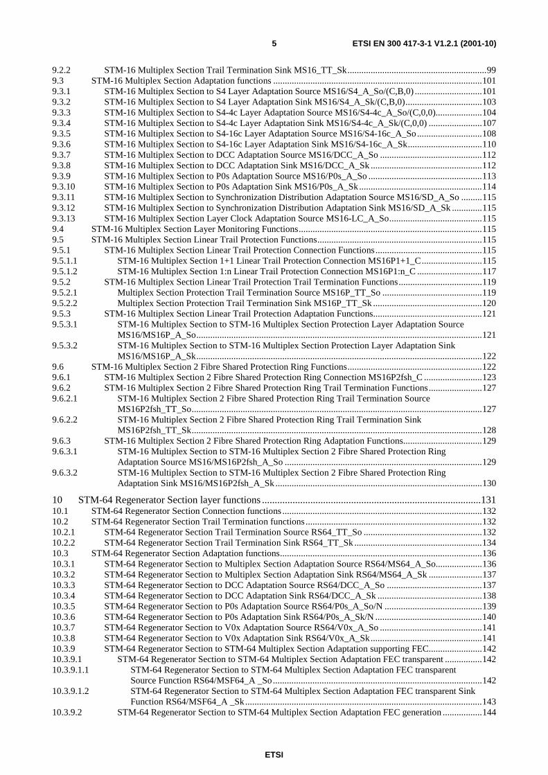
4 STM-1 Regenerator Section Layer Functions
RS1
RS1/MS1
RS1
RS1/MS1
MS1_CI MS1_CI
RS1_CI RS1_CI
RS1/V0x RS1/V0xRS1/P0s-N
P0s_CISTM1_TI
RS1/P0s-N
P0s_CI
E1,F1 E1,F1
V0x_CIV0x_CI
RS1/DCC
DCC_CI
F1 D1-D3
RS1/DCC
DCC_CI
D1-D3 F1 RS1_AI RS1_AI
RS1
Figure 1: STM-1 Regenerator Section atomic functions
ETSI
ETSI EN 300 417-3-1 V1.2.1 (2001-10)15
RS1 Layer CP
The CI at this point is an octet structured, 125 µs framed data stream with co-directional timing. It is the entire STM-1 signal as defined in EN 300 147 [1]. Figure 2 depicts only bytes handled in the RS1 layer.
NOTE 1: The unmarked bytes [2, 6], [3, 6], [3, 8], [3, 9] in rows 2,3 (figure 2) are reserved for future international standardization. Currently, they are undefined.
NOTE 2: The unmarked bytes [2, 2], [2, 3], [2, 5], [3, 2], [3, 3], [3, 5] in rows 2, 3 (figure 2) are reserved for media specific usage (e.g. radio sections). In optical and electrical section applications they are undefined.
NOTE 3: The bytes for National Use (NU) in rows 1,2 (figure 2) are reserved for operator specific usage. Their processing is not within the province of the present document. If NU bytes [1, 8] and [1, 9] are unused, care should be taken in selecting the binary content of the bytes which are excluded from the scrambling process of the STM-N signal to ensure that long sequences of "1"s or "0"s do not occur.
1 2 3 4 5 6 7 8 9 10 .... 270 1 A1 A1 A1 A2 A2 A2 J0 NU NU 2 B1 E1 F1 NU NU 3 D1 D2 D3 4 5 6 MS1_CI 7 8 9
Figure 2: RS1_CI_D signal
RS1 Layer AP
The AI at this point is octet structured and 125 µs framed with co-directional timing and represents the combination of adapted information from the MS1 layer (2 403 bytes per frame), the management communication DCC layer (3 bytes per frame if supported), the OW layer (1 byte per frame if supported) and the user channel F1 (1 byte per frame if supported). The location of these four components in the frame is defined in EN 300 147 [1] and depicted in figure 3.
NOTE 4: Bytes E1, F1 and D1-D3 will be undefined when the adaptation functions sourcing these bytes are not present in the network element.
1 2 3 4 5 6 7 8 9 10 .... 270 1 NU NU 2 E1 F1 NU NU 3 D1 D2 D3 4 5 6 MS1_CI 7 8 9
Figure 3: RS1_AI_D signal
4.1 STM-1 Regenerator Section Connection functions For further study.
ETSI
ETSI EN 300 417-3-1 V1.2.1 (2001-10)16
4.2 STM-1 Regenerator Section Trail Termination functions
4.2.1 STM-1 Regenerator Section Trail Termination Source RS1_TT_So
Symbol:
RS1
RS1_AI
RS1_CI
RS1_TT_So_MI
Figure 4: RS1_TT_So symbol
Interfaces:
Table 1: RS1_TT_So input and output signals
Input(s) Output(s) RS1_AI_D RS1_AI_CK RS1_AI_FS RS1_TT_So_MI_TxTI
RS1_CI_D RS1_CI_CK
Processes:
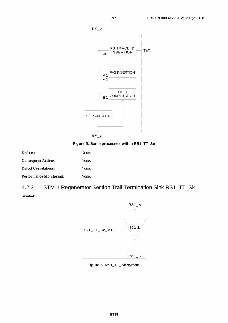
The function builds the STM-1 signal by adding the frame alignment information, bytes A1A2, the STM Section Trace Identifier (STI) byte J0, computing the parity and inserting the B1 byte.
J0: In this byte the function shall insert the Transmitted Trail Trace Identifier TxTI. Its format is described in EN 300 417-1-1 [3], clause 7.1.
B1: The function shall calculate a Bit Interleaved Parity 8 (BIP-8) code using even parity. The BIP-8 shall be calculated over all bits of the previous STM-1 frame after scrambling and is placed in byte position B1 of the current STM-1 frame before scrambling (figure 5).
A1A2: The function shall insert the STM-1 frame alignment signal A1A1A1A2A2A2 into the regenerator section overhead as defined in EN 300 147 [1].
Scrambler: This function provides scrambling of the RS1_CI. The operation of the scrambler shall be functionally identical to that of a frame synchronous scrambler of sequence length 127 operating at the line rate. The generating polynomial shall be 1 + X6 + X7. The scrambler shall be reset to "1111 1111" on the most significant bit (MSB) of the byte [1, 10] following the last byte of the STM-1 SOH in the first row. This bit and all subsequent bits to be scrambled shall be modulo 2 added to the output of the X7 position of the scrambler. The scrambler shall run continuously throughout the remaining STM-1 frame.
ETSI
ETSI EN 300 417-3-1 V1.2.1 (2001-10)17
SCRAMBLER
BIP-8COMPUTATIONB1
R S_CI
RS TRACE IDINSERTIONJ0
FAS INSERTION
RS_AI
A1A2
TxTI
Figure 5: Some processes within RS1_TT_So
Defects: None.
Consequent Actions: None.
Defect Correlations: None.
Performance Monitoring: None.
4.2.2 STM-1 Regenerator Section Trail Termination Sink RS1_TT_Sk
Symbol:
R S 1
RS1_AI
RS1_C I
R S1_TT_Sk_M I
Figure 6: RS1_TT_Sk symbol
ETSI
ETSI EN 300 417-3-1 V1.2.1 (2001-10)18
Interfaces:
Table 2: RS1_TT_Sk input and output signals
Input(s) Output(s) RS1_CI_D RS1_CI_CK RS1_CI_FS RS1_CI_SSF RS1_TT_Sk_MI_ExTI RS1_TT_Sk_MI_TPmode RS1_TT_Sk_MI_TIMdis RS1_TT_Sk_MI_ExTImode RS1_TT_Sk_MI_1second
RS1_AI_D RS1_AI_CK RS1_AI_FS RS1_AI_TSF RS1_TT_Sk_MI_AcTI RS1_TT_Sk_MI_cTIM RS1_TT_Sk_MI_pN_EBC RS1_TT_Sk_MI_pN_DS
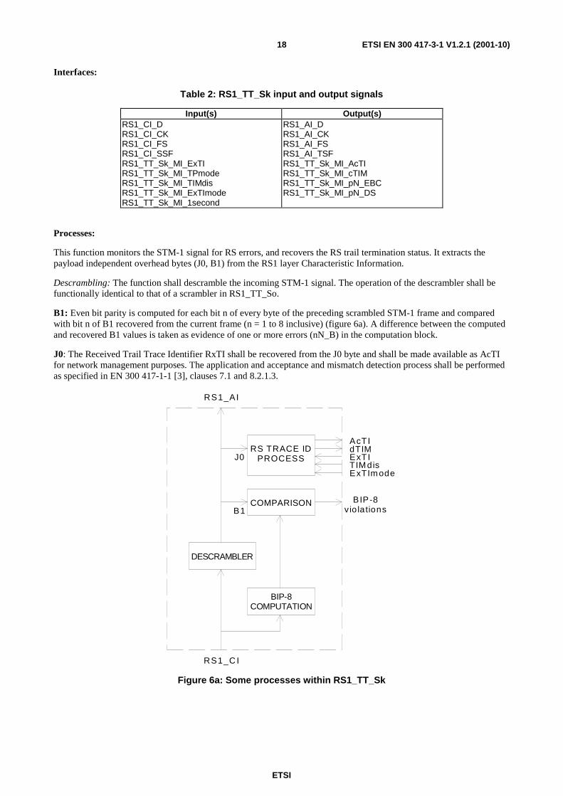
Processes:
This function monitors the STM-1 signal for RS errors, and recovers the RS trail termination status. It extracts the payload independent overhead bytes (J0, B1) from the RS1 layer Characteristic Information.
Descrambling: The function shall descramble the incoming STM-1 signal. The operation of the descrambler shall be functionally identical to that of a scrambler in RS1_TT_So.
B1: Even bit parity is computed for each bit n of every byte of the preceding scrambled STM-1 frame and compared with bit n of B1 recovered from the current frame (n = 1 to 8 inclusive) (figure 6a). A difference between the computed and recovered B1 values is taken as evidence of one or more errors (nN_B) in the computation block.
J0: The Received Trail Trace Identifier RxTI shall be recovered from the J0 byte and shall be made available as AcTI for network management purposes. The application and acceptance and mismatch detection process shall be performed as specified in EN 300 417-1-1 [3], clauses 7.1 and 8.2.1.3.
DESCRAMBLER
BIP-8COMPUTATION
B1
J0
RS1_C I
COMPARISON BIP-8vio lations
AcTIdTIMExTI
RS1_AI
TIM dis
RS TRACE IDPROCESS
ExTIm ode
Figure 6a: Some processes within RS1_TT_Sk
ETSI
ETSI EN 300 417-3-1 V1.2.1 (2001-10)19
Defects:
The function shall detect for dTIM defect according the specification in EN 300 417-1-1 [3], clause 8.2.1.
Consequent Actions:
aAIS ← CI_SSF or dTIM.
aTSF ← CI_SSF or dTIM.
On declaration of aAIS the function shall output an all-ONEs (AIS) signal within 250 µs; on clearing of aAIS the function shall output normal data within 250 µs.
NOTE 1: The term "CI_SSF" has been added to the conditions for aAIS while the descrambler function has been moved from the e.g. OS1/RS1_A_Sk to this function. Consequently, an all-ONEs (AIS) pattern inserted in the mentioned adaptation function would be descrambled in this function. A "refreshment" of all-ONEs is required.
NOTE 2: The insertion of AIS - especially due to detection of dTIM - will cause the RS-DCC channel to be "squelched" too, so that control of the NE via this channel is lost. If control is via this channel only, there is a risk of a dead-lock situation if dTIM is caused by a misprovisioning of ExTI.
Defect Correlations:
cTIM ← MON and dTIM.
Performance Monitoring:
For further study.
4.3 STM-1 Regenerator Section Adaptation functions
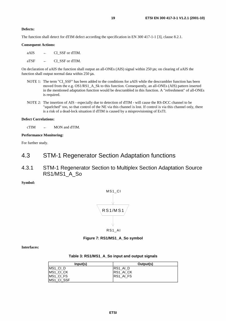
4.3.1 STM-1 Regenerator Section to Multiplex Section Adaptation Source RS1/MS1_A_So
Symbol:
R S 1 /M S 1
MS1_CI
RS1_AI
Figure 7: RS1/MS1_A_So symbol
Interfaces:
Table 3: RS1/MS1_A_So input and output signals
Input(s) Output(s) MS1_CI_D MS1_CI_CK MS1_CI_FS MS1_CI_SSF
RS1_AI_D RS1_AI_CK RS1_AI_FS
ETSI
ETSI EN 300 417-3-1 V1.2.1 (2001-10)20
Processes:
The function multiplexes the MS1_CI data (2 403 bytes / frame) into the STM-1 byte locations defined in EN 300 147 [1] and depicted in figure 3.
NOTE 1: There might be cases in which the network element knows that the timing reference for a particular STM-1 interface can not be maintained within ±4,6 ppm. For such cases MS-AIS can be generated. This is network element specific and outside the scope of the present document.
Defects: None.
Consequent Actions:
aAIS ← CI_SSF.
On declaration of aAIS the function shall output all ONEs signal within 250 µs; on clearing of aAIS the function shall output normal data within 250 µs. The frequency of the all ONEs signal shall be within 155 520 kHz ± 20 ppm.
NOTE 2: If CI_SSF is not connected (when RS1/MS1_A_So is connected to a MS1_TT_So), SSF is assumed to be false.
Defect Correlations: None.
Performance Monitoring: None.
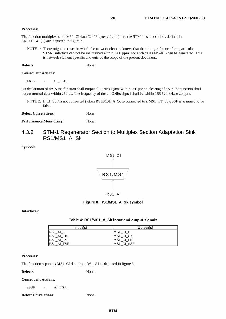
4.3.2 STM-1 Regenerator Section to Multiplex Section Adaptation Sink RS1/MS1_A_Sk
Symbol:
R S 1 /M S 1
MS1_CI
RS1_AI
Figure 8: RS1/MS1_A_Sk symbol
Interfaces:
Table 4: RS1/MS1_A_Sk input and output signals
Input(s) Output(s) RS1_AI_D RS1_AI_CK RS1_AI_FS RS1_AI_TSF
MS1_CI_D MS1_CI_CK MS1_CI_FS MS1_CI_SSF
Processes:
The function separates MS1_CI data from RS1_AI as depicted in figure 3.
Defects: None.
Consequent Actions:
aSSF ← AI_TSF.
Defect Correlations: None.
ETSI
ETSI EN 300 417-3-1 V1.2.1 (2001-10)21
Performance Monitoring: None.
4.3.3 STM-1 Regenerator Section to DCC Adaptation Source RS1/DCC_A_So
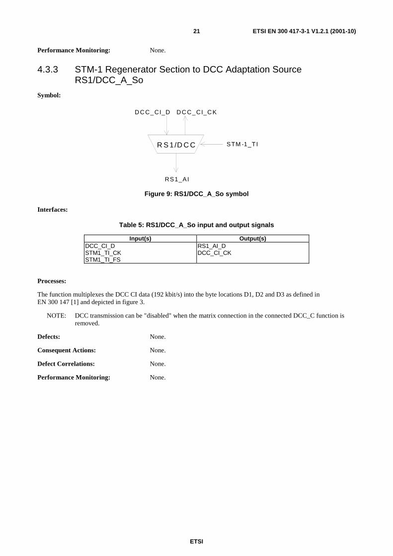
Symbol:
R S 1/D C C
D C C_CI_D
RS1_AI
STM -1_TI
D C C_CI_C K
Figure 9: RS1/DCC_A_So symbol
Interfaces:
Table 5: RS1/DCC_A_So input and output signals
Input(s) Output(s) DCC_CI_D STM1_TI_CK STM1_TI_FS
RS1_AI_D DCC_CI_CK
Processes:
The function multiplexes the DCC CI data (192 kbit/s) into the byte locations D1, D2 and D3 as defined in EN 300 147 [1] and depicted in figure 3.
NOTE: DCC transmission can be "disabled" when the matrix connection in the connected DCC_C function is removed.
Defects: None.
Consequent Actions: None.
Defect Correlations: None.
Performance Monitoring: None.
ETSI
ETSI EN 300 417-3-1 V1.2.1 (2001-10)22
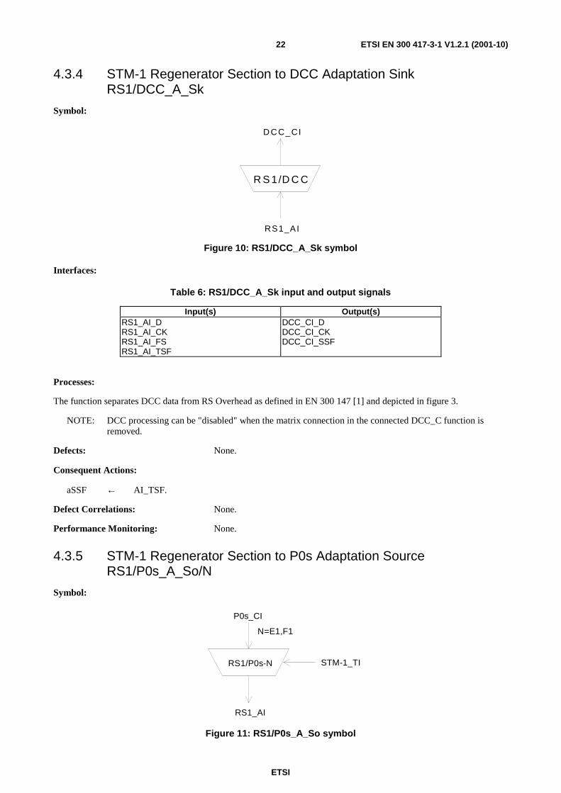
4.3.4 STM-1 Regenerator Section to DCC Adaptation Sink RS1/DCC_A_Sk
Symbol:
R S 1/D C C
D C C_CI
RS1_AI
Figure 10: RS1/DCC_A_Sk symbol
Interfaces:
Table 6: RS1/DCC_A_Sk input and output signals
Input(s) Output(s) RS1_AI_D RS1_AI_CK RS1_AI_FS RS1_AI_TSF
DCC_CI_D DCC_CI_CK DCC_CI_SSF
Processes:
The function separates DCC data from RS Overhead as defined in EN 300 147 [1] and depicted in figure 3.
NOTE: DCC processing can be "disabled" when the matrix connection in the connected DCC_C function is removed.
Defects: None.
Consequent Actions:
aSSF ← AI_TSF.
Defect Correlations: None.
Performance Monitoring: None.
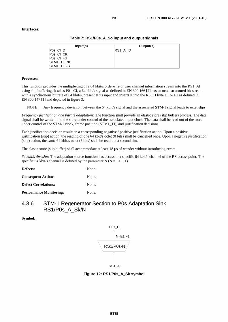
4.3.5 STM-1 Regenerator Section to P0s Adaptation Source RS1/P0s_A_So/N
Symbol:
RS1/P0s-N
P0s_CI
RS1_AI
STM-1_TI
N=E1,F1
Figure 11: RS1/P0s_A_So symbol
ETSI
ETSI EN 300 417-3-1 V1.2.1 (2001-10)23
Interfaces:
Table 7: RS1/P0s_A_So input and output signals
Input(s) Output(s) P0s_CI_D P0s_CI_CK P0s_CI_FS STM1_TI_CK STM1_TI_FS
RS1_AI_D
Processes:
This function provides the multiplexing of a 64 kbit/s orderwire or user channel information stream into the RS1_AI using slip buffering. It takes P0s_CI, a 64 kbit/s signal as defined in EN 300 166 [2] , as an octet structured bit-stream with a synchronous bit rate of 64 kbit/s, present at its input and inserts it into the RSOH byte E1 or F1 as defined in EN 300 147 [1] and depicted in figure 3.
NOTE: Any frequency deviation between the 64 kbit/s signal and the associated STM-1 signal leads to octet slips.
Frequency justification and bitrate adaptation: The function shall provide an elastic store (slip buffer) process. The data signal shall be written into the store under control of the associated input clock. The data shall be read out of the store under control of the STM-1 clock, frame position (STM1_TI), and justification decisions.
Each justification decision results in a corresponding negative / positive justification action. Upon a positive justification (slip) action, the reading of one 64 kbit/s octet (8 bits) shall be cancelled once. Upon a negative justification (slip) action, the same 64 kbit/s octet (8 bits) shall be read out a second time.
The elastic store (slip buffer) shall accommodate at least 18 µs of wander without introducing errors.
64 kbit/s timeslot: The adaptation source function has access to a specific 64 kbit/s channel of the RS access point. The specific 64 kbit/s channel is defined by the parameter N (N = E1, F1).
Defects: None.
Consequent Actions: None.
Defect Correlations: None.
Performance Monitoring: None.
4.3.6 STM-1 Regenerator Section to P0s Adaptation Sink RS1/P0s_A_Sk/N
Symbol:
RS1/P0s-N
P0s_CI
RS1_AI
N=E1,F1
Figure 12: RS1/P0s_A_Sk symbol
ETSI
ETSI EN 300 417-3-1 V1.2.1 (2001-10)24
Interfaces:
Table 8: RS1/P0s_A_Sk input and output signals
Input(s) Output(s) RS1_AI_D RS1_AI_CK RS1_AI_FS RS1_AI_TSF
P0s_CI_D P0s_CI_CK P0s_CI_FS P0s_CI_SSF
Processes:
The function separates P0s data from RS Overhead byte E1 or F1 as defined in EN 300 147 [1] and depicted in figure 3.
Data latching and smoothing process: The function shall provide a data latching and smoothing function. Each 8-bit octet received shall be written and latched into a data store under the control of the STM-1 signal clock. The eight data bits shall then be read out of the store using a nominal 64 kHz clock which may be derived directly from the incoming STM-1 signal clock (e.g. 155 520 kHz divided by a factor of 2 430).
64 kbit/s timeslot: The adaptation sink function has access to a specific 64 kbit/s of the RS access point. The specific 64 kbit/s is defined by the parameter N (N = E1, F1).
Defects: None.
Consequent Actions:
aSSF ← AI_TSF.
aAIS ← AI_TSF.
On declaration of aAIS the function shall output an all-ONEs (AIS) signal - complying with the frequency limits for this signal (a bit rate in range 64 kbit/s ± 100 ppm) - within 1 ms; on clearing of aAIS the function shall output normal data within 1 ms.
Defect Correlations: None.
Performance Monitoring: None.
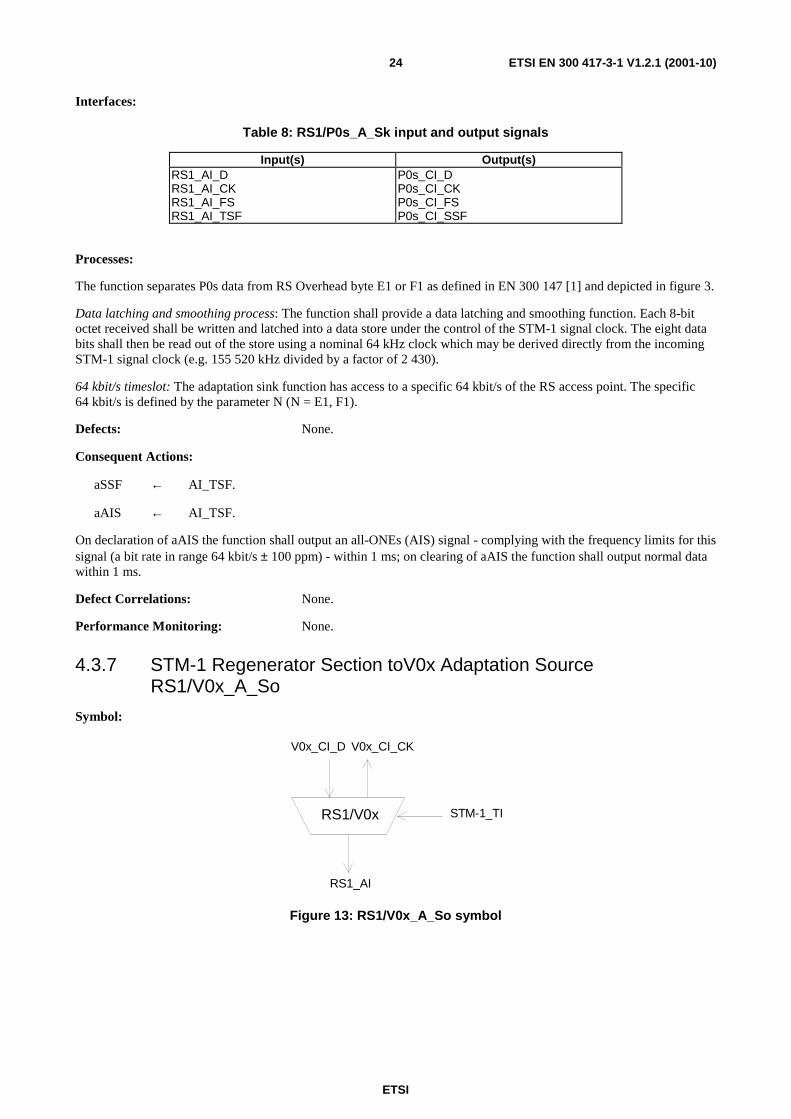
4.3.7 STM-1 Regenerator Section toV0x Adaptation Source RS1/V0x_A_So
Symbol:
RS1/V0x
RS1_AI
STM-1_TI
V0x_CI_CKV0x_CI_D
Figure 13: RS1/V0x_A_So symbol
ETSI
ETSI EN 300 417-3-1 V1.2.1 (2001-10)25
Interfaces:
Table 9: RS1/V0x_A_So input and output signals
Input(s) Output(s) V0x_CI_D STM1_TI_CK STM1_TI_FS
RS1_AI_D V0x_CI_CK
Processes: None.
This function shall multiplex the V0x_CI data (64 kbit/s) into the byte location F1 as defined in EN 300 147 [1] and depicted in figure 3.
Defects: None.
Consequent Actions: None.
Defect Correlations: None.
Performance Monitoring: None.
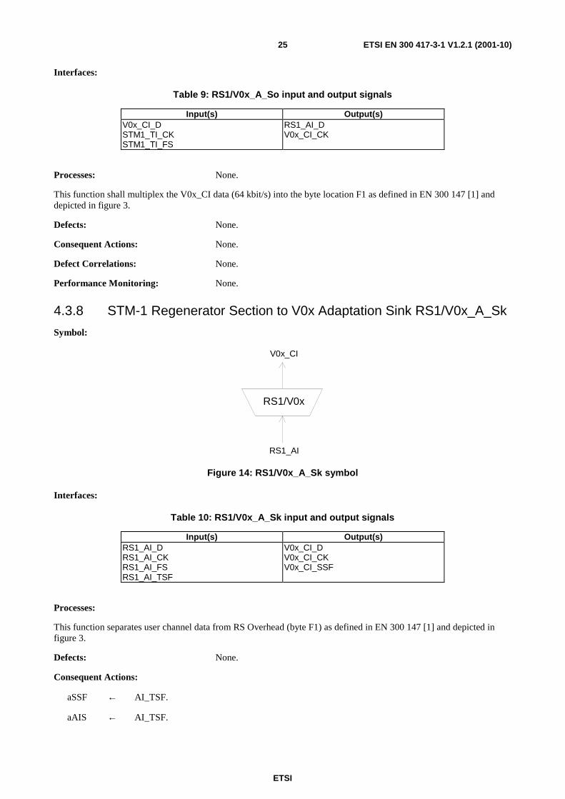
4.3.8 STM-1 Regenerator Section to V0x Adaptation Sink RS1/V0x_A_Sk
Symbol:
RS1/V0x
V0x_CI
RS1_AI
Figure 14: RS1/V0x_A_Sk symbol
Interfaces:
Table 10: RS1/V0x_A_Sk input and output signals
Input(s) Output(s) RS1_AI_D RS1_AI_CK RS1_AI_FS RS1_AI_TSF
V0x_CI_D V0x_CI_CK V0x_CI_SSF
Processes:
This function separates user channel data from RS Overhead (byte F1) as defined in EN 300 147 [1] and depicted in figure 3.
Defects: None.
Consequent Actions:
aSSF ← AI_TSF.
aAIS ← AI_TSF.
ETSI
ETSI EN 300 417-3-1 V1.2.1 (2001-10)26
On declaration of aAIS the function shall output an all-ONEs (AIS) signal within 1 ms; on clearing of aAIS the function shall output normal data within 1 ms.
Defect Correlations: None.
Performance Monitoring: None.
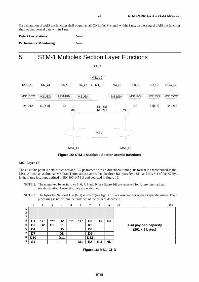
5 STM-1 Multiplex Section Layer Functions
MS1
MS1/S4
MS1
MS1/S4
S4_CI S4_CI
MS1_CI MS1_CI
MS1/SD MS1/SDMS1/P0s
P0s_CISTM1_TI
MS1/P0s
P0s_CI
E2 E2
SD_CISD_CI
MS1/DCC
DCC_CI
S1[5-8] D4-D12
MS1/DCC
DCC_CI
D4-D12 S1[5-8] RI_RDIRI_REI
MS1-LC
SD_CI
MS1
Figure 15: STM-1 Multiplex Section atomic functions
MS1 Layer CP
The CI at this point is octet structured and 125 µs framed with co-directional timing. Its format is characterized as the MS1_AI with an additional MS Trail Termination overhead in the three B2 bytes, byte M1, and bits 6-8 of the K2 byte in the frame locations defined in EN 300 147 [1] and depicted in figure 16.
NOTE 1: The unmarked bytes in rows 5, 6, 7, 8 and 9 (see figure 16) are reserved for future international standardization. Currently, they are undefined.
NOTE 2: The bytes for National Use (NU) in row 9 (see figure 16) are reserved for operator specific usage. Their processing is not within the province of the present document.
1 2 3 4 5 6 7 8 9 10 .... 270 1 2 3 4 H1 "Y" "Y" H2 "1" "1" H3 H3 H3 5 B2 B2 B2 K1 K2 AU4 payload capacity 6 D4 D5 D6 (261 ×××× 9 bytes) 7 D7 D8 D9 8 D10 D11 D12 9 S1 M1 E2 NU NU
Figure 16: MS1_CI_D
ETSI
ETSI EN 300 417-3-1 V1.2.1 (2001-10)27
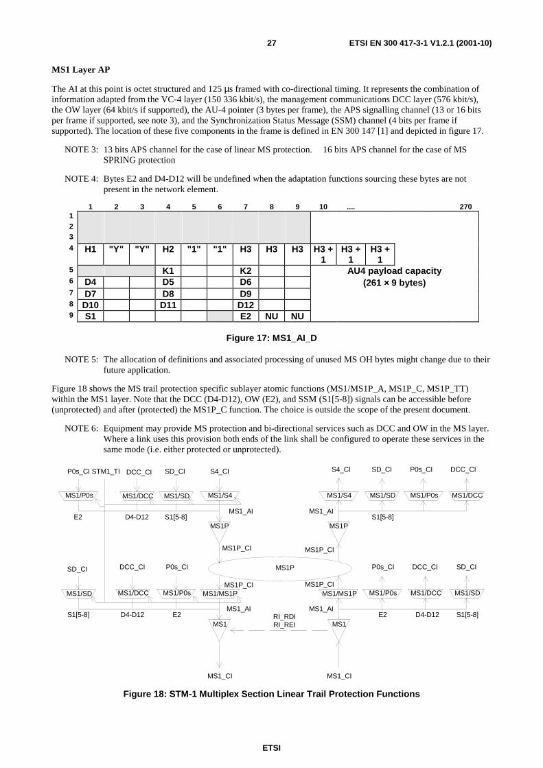
MS1 Layer AP
The AI at this point is octet structured and 125 µs framed with co-directional timing. It represents the combination of information adapted from the VC-4 layer (150 336 kbit/s), the management communications DCC layer (576 kbit/s), the OW layer (64 kbit/s if supported), the AU-4 pointer (3 bytes per frame), the APS signalling channel (13 or 16 bits per frame if supported, see note 3), and the Synchronization Status Message (SSM) channel (4 bits per frame if supported). The location of these five components in the frame is defined in EN 300 147 [1] and depicted in figure 17.
NOTE 3: 13 bits APS channel for the case of linear MS protection. 16 bits APS channel for the case of MS SPRING protection
NOTE 4: Bytes E2 and D4-D12 will be undefined when the adaptation functions sourcing these bytes are not present in the network element.
1 2 3 4 5 6 7 8 9 10 .... 270 1 2 3 4 H1 "Y" "Y" H2 "1" "1" H3 H3 H3 H3 +
1 H3 +
1 H3 +
1
5 K1 K2 AU4 payload capacity 6 D4 D5 D6 (261 ×××× 9 bytes) 7 D7 D8 D9 8 D10 D11 D12 9 S1 E2 NU NU
Figure 17: MS1_AI_D
NOTE 5: The allocation of definitions and associated processing of unused MS OH bytes might change due to their future application.
Figure 18 shows the MS trail protection specific sublayer atomic functions (MS1/MS1P_A, MS1P_C, MS1P_TT) within the MS1 layer. Note that the DCC (D4-D12), OW (E2), and SSM (S1[5-8]) signals can be accessible before (unprotected) and after (protected) the MS1P_C function. The choice is outside the scope of the present document.
NOTE 6: Equipment may provide MS protection and bi-directional services such as DCC and OW in the MS layer. Where a link uses this provision both ends of the link shall be configured to operate these services in the same mode (i.e. either protected or unprotected).
MS1
MS1/MS1P
MS1
MS1/MS1P
MS1P
MS1_CI MS1_CI
MS1/P0s
P0s_CI
STM1_TI
MS1/P0s
P0s_CI
E2 E2
MS1/DCC
DCC_CI
D4-D12
MS1/DCC
DCC_CI
D4-D12 RI_RDIRI_REI
MS1/S4
S4_CI
MS1/S4
S4_CI
MS1/SD
SD_CI
S1[5-8]
MS1/SD
SD_CI
S1[5-8]MS1P MS1P
MS1/DCC
DCC_CI
D4-D12
MS1/P0s
P0s_CI
E2
MS1/P0s MS1/DCC
P0s_CI DCC_CI
MS1/SD
SD_CI
S1[5-8]
MS1/SD
SD_CI
S1[5-8]
MS1P_CI
MS1P_CI
MS1P_CI
MS1P_CI
MS1_AIMS1_AI
MS1_AI MS1_AI
Figure 18: STM-1 Multiplex Section Linear Trail Protection Functions
ETSI
ETSI EN 300 417-3-1 V1.2.1 (2001-10)28
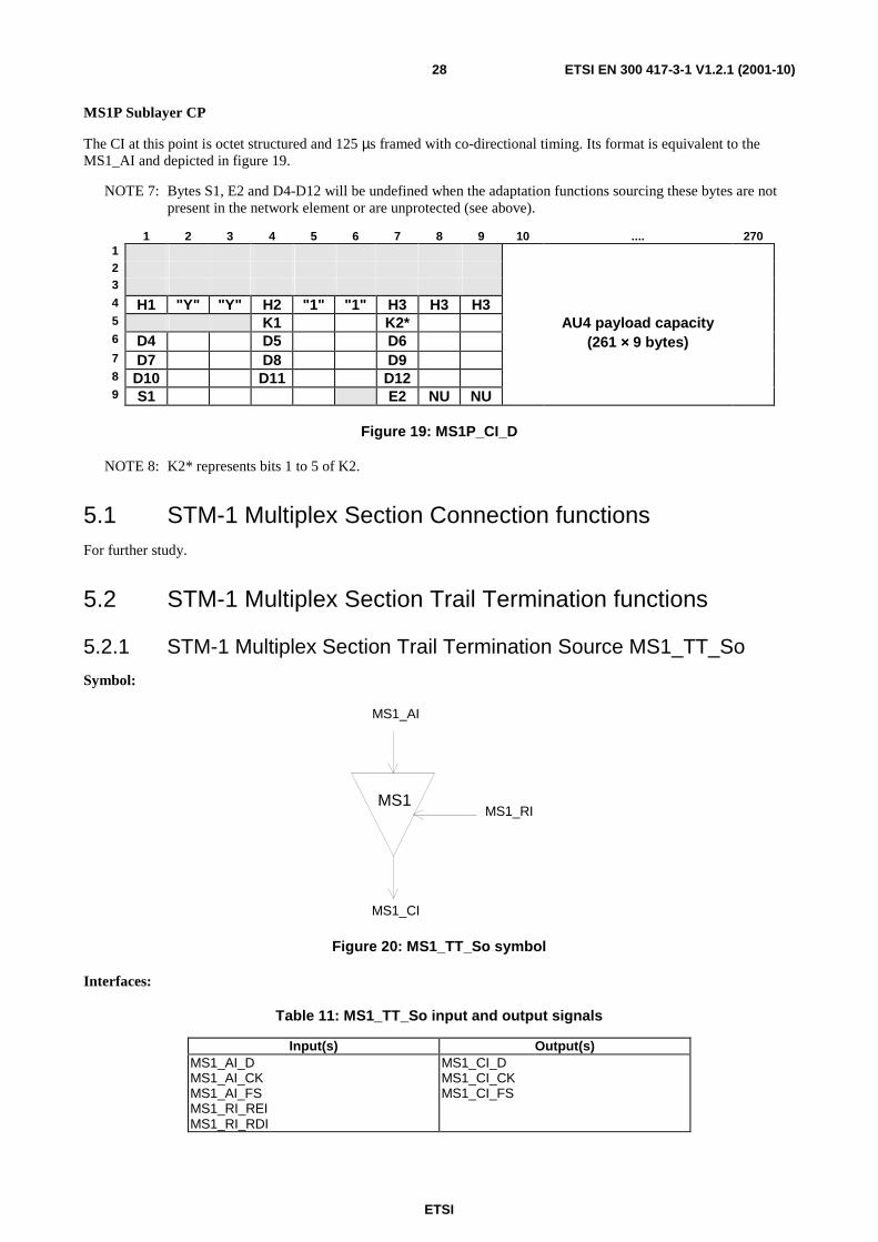
MS1P Sublayer CP
The CI at this point is octet structured and 125 µs framed with co-directional timing. Its format is equivalent to the MS1_AI and depicted in figure 19.
NOTE 7: Bytes S1, E2 and D4-D12 will be undefined when the adaptation functions sourcing these bytes are not present in the network element or are unprotected (see above).
1 2 3 4 5 6 7 8 9 10 .... 270 1 2 3 4 H1 "Y" "Y" H2 "1" "1" H3 H3 H3 5 K1 K2* AU4 payload capacity 6 D4 D5 D6 (261 ×××× 9 bytes) 7 D7 D8 D9 8 D10 D11 D12 9 S1 E2 NU NU
Figure 19: MS1P_CI_D
NOTE 8: K2* represents bits 1 to 5 of K2.
5.1 STM-1 Multiplex Section Connection functions For further study.
5.2 STM-1 Multiplex Section Trail Termination functions
5.2.1 STM-1 Multiplex Section Trail Termination Source MS1_TT_So
Symbol:
MS1
MS1_AI
MS1_CI
MS1_RI
Figure 20: MS1_TT_So symbol
Interfaces:
Table 11: MS1_TT_So input and output signals
Input(s) Output(s) MS1_AI_D MS1_AI_CK MS1_AI_FS MS1_RI_REI MS1_RI_RDI
MS1_CI_D MS1_CI_CK MS1_CI_FS
ETSI
ETSI EN 300 417-3-1 V1.2.1 (2001-10)29
Processes:
This function adds error monitoring capabilities and remote maintenance information signals to the MS1_AI.
M1: The function shall within 1 ms insert the value of MS1_RI_REI into the REI (Remote Error Indication) - to convey the count of interleaved bit blocks that have been detected in error by the BIP-24 process in the companion MS1_TT_Sk - in the range of "0000 0000" (0) to "0001 1000" (24).
K2[6-8]: These bits represents the defect status of the associated MS1_TT_Sk. The RDI indication shall be set to "110" on activation of MS1_RI_RDI within 1 ms, determined by the associated MS1_TT_Sk function, and set to "000" within 1 ms on the clearing of MS1_RI_RDI.
B2: The function shall calculate a Bit Interleaved Parity 24 (BIP-24) code using even parity. The BIP-24 shall be calculated over all bits, except those in the RSOH bytes, of the previous STM-1 frame and placed in three B2 bytes of the current STM-1 frame.
NOTE: The BIP-24 procedure is described in EN 300 147 [1].
Defects: None.
Consequent Actions: None.
Defect Correlations: None.
Performance Monitoring: None.
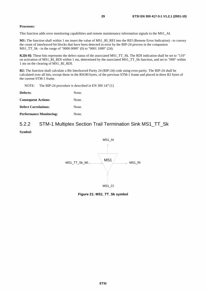
5.2.2 STM-1 Multiplex Section Trail Termination Sink MS1_TT_Sk
Symbol:
MS1
MS1_AI
MS1_CI
MS1_TT_Sk_MI MS1_RI
Figure 21: MS1_TT_Sk symbol
ETSI
ETSI EN 300 417-3-1 V1.2.1 (2001-10)30
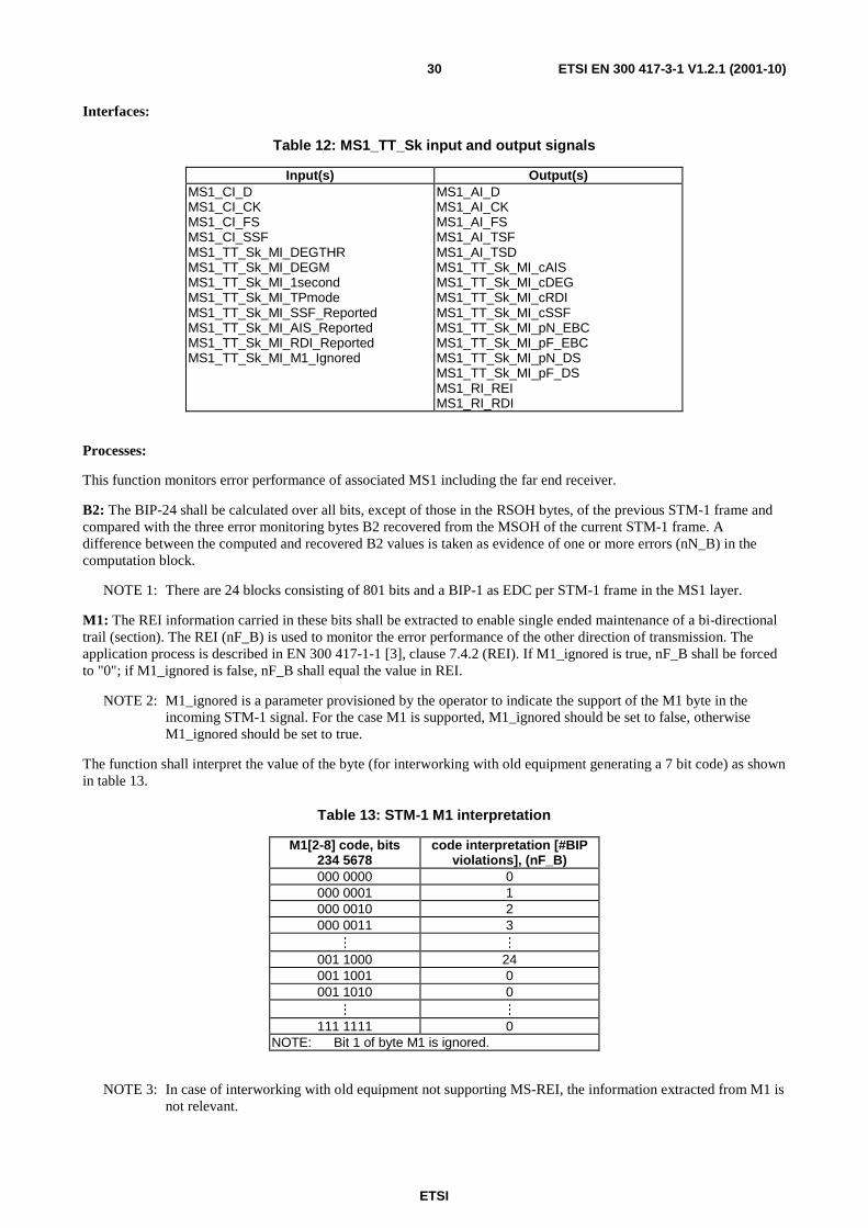
Interfaces:
Table 12: MS1_TT_Sk input and output signals
Input(s) Output(s) MS1_CI_D MS1_CI_CK MS1_CI_FS MS1_CI_SSF MS1_TT_Sk_MI_DEGTHR MS1_TT_Sk_MI_DEGM MS1_TT_Sk_MI_1second MS1_TT_Sk_MI_TPmode MS1_TT_Sk_MI_SSF_Reported MS1_TT_Sk_MI_AIS_Reported MS1_TT_Sk_MI_RDI_Reported MS1_TT_Sk_MI_M1_Ignored
MS1_AI_D MS1_AI_CK MS1_AI_FS MS1_AI_TSF MS1_AI_TSD MS1_TT_Sk_MI_cAIS MS1_TT_Sk_MI_cDEG MS1_TT_Sk_MI_cRDI MS1_TT_Sk_MI_cSSF MS1_TT_Sk_MI_pN_EBC MS1_TT_Sk_MI_pF_EBC MS1_TT_Sk_MI_pN_DS MS1_TT_Sk_MI_pF_DS MS1_RI_REI MS1_RI_RDI
Processes:
This function monitors error performance of associated MS1 including the far end receiver.
B2: The BIP-24 shall be calculated over all bits, except of those in the RSOH bytes, of the previous STM-1 frame and compared with the three error monitoring bytes B2 recovered from the MSOH of the current STM-1 frame. A difference between the computed and recovered B2 values is taken as evidence of one or more errors (nN_B) in the computation block.
NOTE 1: There are 24 blocks consisting of 801 bits and a BIP-1 as EDC per STM-1 frame in the MS1 layer.
M1: The REI information carried in these bits shall be extracted to enable single ended maintenance of a bi-directional trail (section). The REI (nF_B) is used to monitor the error performance of the other direction of transmission. The application process is described in EN 300 417-1-1 [3], clause 7.4.2 (REI). If M1_ignored is true, nF_B shall be forced to "0"; if M1_ignored is false, nF_B shall equal the value in REI.
NOTE 2: M1_ignored is a parameter provisioned by the operator to indicate the support of the M1 byte in the incoming STM-1 signal. For the case M1 is supported, M1_ignored should be set to false, otherwise M1_ignored should be set to true.
The function shall interpret the value of the byte (for interworking with old equipment generating a 7 bit code) as shown in table 13.
Table 13: STM-1 M1 interpretation
M1[2-8] code, bits 234 5678
code interpretation [#BIP violations], (nF_B)
000 0000 0 000 0001 1 000 0010 2 000 0011 3
M M 001 1000 24 001 1001 0 001 1010 0
M M 111 1111 0
NOTE: Bit 1 of byte M1 is ignored.
NOTE 3: In case of interworking with old equipment not supporting MS-REI, the information extracted from M1 is not relevant.
ETSI
ETSI EN 300 417-3-1 V1.2.1 (2001-10)31
K2[6-8] - RDI: The RDI information carried in these bits shall be extracted to enable single ended maintenance of a bi-directional trail (section). The RDI provides information as to the status of the remote receiver. A "110" indicates a Remote Defect Indication state, while other patterns indicate the normal state. The application process is described in EN 300 417-1-1 [3], clauses 7.4.11 and 8.2.
K2[6-8] - AIS: The MS-AIS information carried in these bits shall be extracted.
Defects:
The function shall detect for dDEG and dRDI defects according the specification in EN 300 417-1-1 [3], clause 8.2.1.
dAIS: If at least x consecutive frames contain the "111" pattern in bits 6, 7 and 8 of the K2 byte a dAIS defect shall be detected. dAIS shall be cleared if in at least x consecutive frames any pattern other then the "111" is detected in bits 6, 7 and 8 of byte K2. The x is in range 3 to 5.
Consequent Actions:
aAIS ← dAIS.
aRDI ← dAIS.
aREI ← #EDCV.
aTSF ← dAIS.
aTSD ← dDEG.
On declaration of aAIS the function shall output an all-ONEs signal within 250 µs; on clearing of aAIS the function shall output normal data within 250 µs.
Defect Correlations:
cAIS ← MON and dAIS and (not CI_SSF) and AIS_Reported.
cDEG ← MON and dDEG.
cRDI ← MON and dRDI and RDI_Reported.
cSSF ← MON and dAIS and SSF_Reported.
Performance monitoring:
The performance monitoring process shall be performed as specified in EN 300 417-1-1 [3], clause 8.2.4 through 8.2.7.
pN_DS ← aTSF or dEQ.
pF_DS ← dRDI.
pN_EBC ← Σ nN_B.
pF_EBC ← Σ nF_B.
ETSI
ETSI EN 300 417-3-1 V1.2.1 (2001-10)32
5.3 STM-1 Multiplex Section Adaptation functions
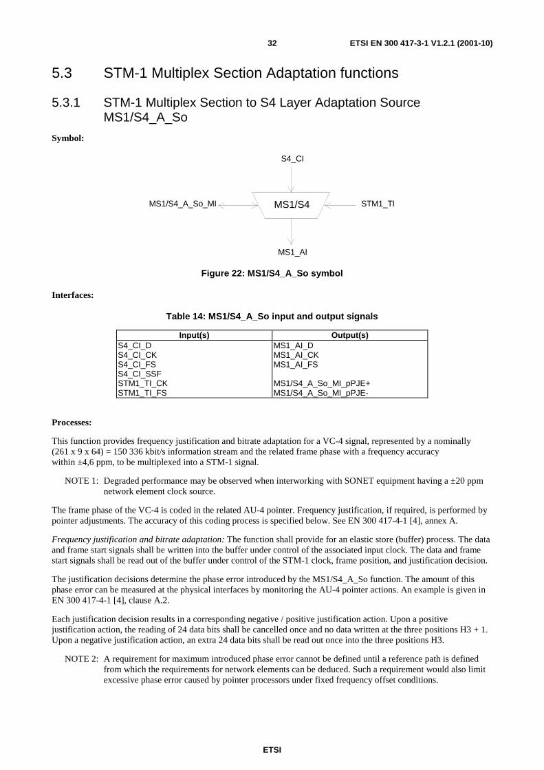
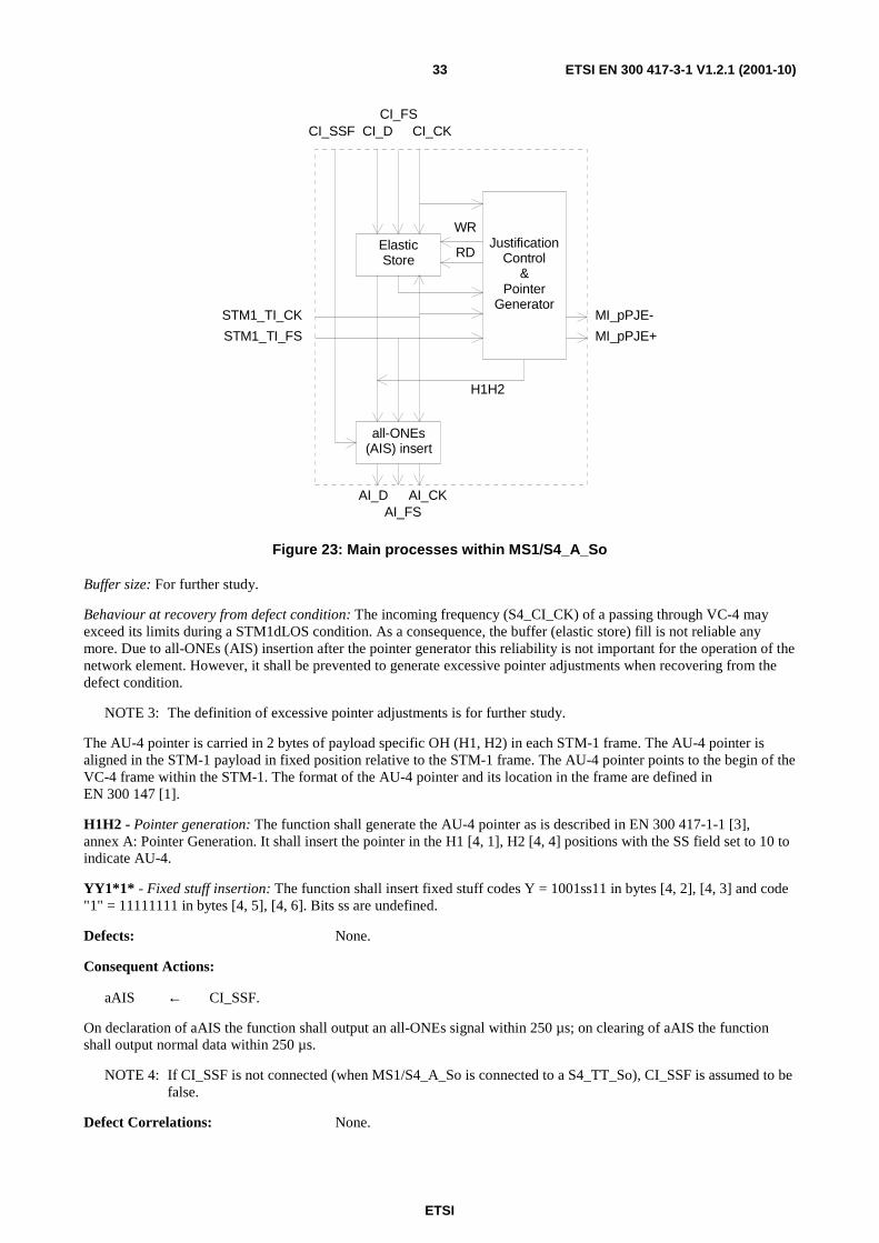
5.3.1 STM-1 Multiplex Section to S4 Layer Adaptation Source MS1/S4_A_So
Symbol:
MS1/S4
S4_CI
MS1_AI
MS1/S4_A_So_MI STM1_TI
Figure 22: MS1/S4_A_So symbol
Interfaces:
Table 14: MS1/S4_A_So input and output signals
Input(s) Output(s) S4_CI_D S4_CI_CK S4_CI_FS S4_CI_SSF STM1_TI_CK STM1_TI_FS
MS1_AI_D MS1_AI_CK MS1_AI_FS MS1/S4_A_So_MI_pPJE+ MS1/S4_A_So_MI_pPJE-
Processes:
This function provides frequency justification and bitrate adaptation for a VC-4 signal, represented by a nominally (261 x 9 x 64) = 150 336 kbit/s information stream and the related frame phase with a frequency accuracy within ±4,6 ppm, to be multiplexed into a STM-1 signal.
NOTE 1: Degraded performance may be observed when interworking with SONET equipment having a ±20 ppm network element clock source.
The frame phase of the VC-4 is coded in the related AU-4 pointer. Frequency justification, if required, is performed by pointer adjustments. The accuracy of this coding process is specified below. See EN 300 417-4-1 [4], annex A.
Frequency justification and bitrate adaptation: The function shall provide for an elastic store (buffer) process. The data and frame start signals shall be written into the buffer under control of the associated input clock. The data and frame start signals shall be read out of the buffer under control of the STM-1 clock, frame position, and justification decision.
The justification decisions determine the phase error introduced by the MS1/S4_A_So function. The amount of this phase error can be measured at the physical interfaces by monitoring the AU-4 pointer actions. An example is given in EN 300 417-4-1 [4], clause A.2.
Each justification decision results in a corresponding negative / positive justification action. Upon a positive justification action, the reading of 24 data bits shall be cancelled once and no data written at the three positions H3 + 1. Upon a negative justification action, an extra 24 data bits shall be read out once into the three positions H3.
NOTE 2: A requirement for maximum introduced phase error cannot be defined until a reference path is defined from which the requirements for network elements can be deduced. Such a requirement would also limit excessive phase error caused by pointer processors under fixed frequency offset conditions.
ETSI
ETSI EN 300 417-3-1 V1.2.1 (2001-10)33
ElasticStore
JustificationControl
&Pointer
Generator
STM1_TI_FS
STM1_TI_CK
WR
RD
all-ONEs(AIS) insert
CI_SSF CI_DCI_FS
CI_CK
AI_DAI_FS
AI_CK
H1H2
MI_pPJE-
MI_pPJE+
Figure 23: Main processes within MS1/S4_A_So
Buffer size: For further study.
Behaviour at recovery from defect condition: The incoming frequency (S4_CI_CK) of a passing through VC-4 may exceed its limits during a STM1dLOS condition. As a consequence, the buffer (elastic store) fill is not reliable any more. Due to all-ONEs (AIS) insertion after the pointer generator this reliability is not important for the operation of the network element. However, it shall be prevented to generate excessive pointer adjustments when recovering from the defect condition.
NOTE 3: The definition of excessive pointer adjustments is for further study.
The AU-4 pointer is carried in 2 bytes of payload specific OH (H1, H2) in each STM-1 frame. The AU-4 pointer is aligned in the STM-1 payload in fixed position relative to the STM-1 frame. The AU-4 pointer points to the begin of the VC-4 frame within the STM-1. The format of the AU-4 pointer and its location in the frame are defined in EN 300 147 [1].
H1H2 - Pointer generation: The function shall generate the AU-4 pointer as is described in EN 300 417-1-1 [3], annex A: Pointer Generation. It shall insert the pointer in the H1 [4, 1], H2 [4, 4] positions with the SS field set to 10 to indicate AU-4.
YY1*1* - Fixed stuff insertion: The function shall insert fixed stuff codes Y = 1001ss11 in bytes [4, 2], [4, 3] and code "1" = 11111111 in bytes [4, 5], [4, 6]. Bits ss are undefined.
Defects: None.
Consequent Actions:
aAIS ← CI_SSF.
On declaration of aAIS the function shall output an all-ONEs signal within 250 µs; on clearing of aAIS the function shall output normal data within 250 µs.
NOTE 4: If CI_SSF is not connected (when MS1/S4_A_So is connected to a S4_TT_So), CI_SSF is assumed to be false.
Defect Correlations: None.
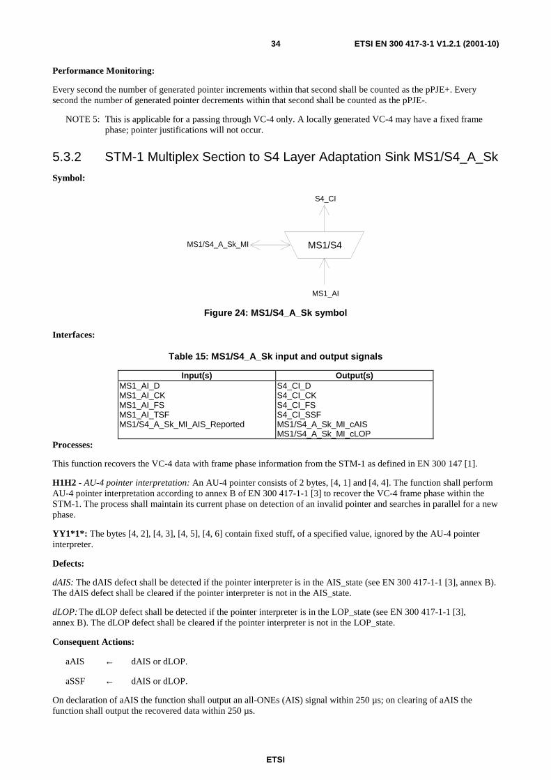
ETSI
ETSI EN 300 417-3-1 V1.2.1 (2001-10)34
Performance Monitoring:
Every second the number of generated pointer increments within that second shall be counted as the pPJE+. Every second the number of generated pointer decrements within that second shall be counted as the pPJE-.
NOTE 5: This is applicable for a passing through VC-4 only. A locally generated VC-4 may have a fixed frame phase; pointer justifications will not occur.
5.3.2 STM-1 Multiplex Section to S4 Layer Adaptation Sink MS1/S4_A_Sk
Symbol:
MS1/S4
S4_CI
MS1_AI
MS1/S4_A_Sk_MI
Figure 24: MS1/S4_A_Sk symbol
Interfaces:
Table 15: MS1/S4_A_Sk input and output signals
Input(s) Output(s) MS1_AI_D MS1_AI_CK MS1_AI_FS MS1_AI_TSF MS1/S4_A_Sk_MI_AIS_Reported
S4_CI_D S4_CI_CK S4_CI_FS S4_CI_SSF MS1/S4_A_Sk_MI_cAIS MS1/S4_A_Sk_MI_cLOP
Processes:
This function recovers the VC-4 data with frame phase information from the STM-1 as defined in EN 300 147 [1].
H1H2 - AU-4 pointer interpretation: An AU-4 pointer consists of 2 bytes, [4, 1] and [4, 4]. The function shall perform AU-4 pointer interpretation according to annex B of EN 300 417-1-1 [3] to recover the VC-4 frame phase within the STM-1. The process shall maintain its current phase on detection of an invalid pointer and searches in parallel for a new phase.
YY1*1*: The bytes [4, 2], [4, 3], [4, 5], [4, 6] contain fixed stuff, of a specified value, ignored by the AU-4 pointer interpreter.
Defects:
dAIS: The dAIS defect shall be detected if the pointer interpreter is in the AIS_state (see EN 300 417-1-1 [3], annex B). The dAIS defect shall be cleared if the pointer interpreter is not in the AIS_state.
dLOP: The dLOP defect shall be detected if the pointer interpreter is in the LOP_state (see EN 300 417-1-1 [3], annex B). The dLOP defect shall be cleared if the pointer interpreter is not in the LOP_state.
Consequent Actions:
aAIS ← dAIS or dLOP.
aSSF ← dAIS or dLOP.
On declaration of aAIS the function shall output an all-ONEs (AIS) signal within 250 µs; on clearing of aAIS the function shall output the recovered data within 250 µs.
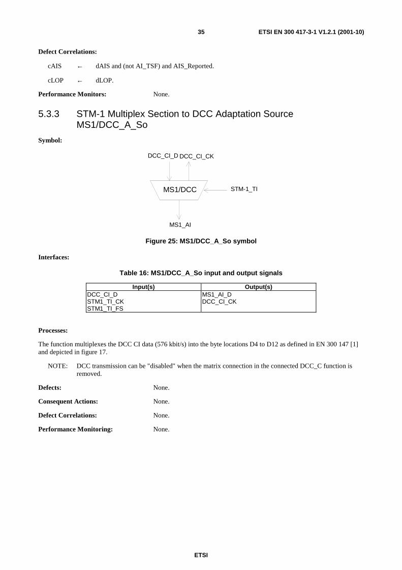
ETSI
ETSI EN 300 417-3-1 V1.2.1 (2001-10)35
Defect Correlations:
cAIS ← dAIS and (not AI_TSF) and AIS_Reported.
cLOP ← dLOP.
Performance Monitors: None.
5.3.3 STM-1 Multiplex Section to DCC Adaptation Source MS1/DCC_A_So
Symbol:
MS1/DCC
DCC_CI_D
MS1_AI
STM-1_TI
DCC_CI_CK
Figure 25: MS1/DCC_A_So symbol
Interfaces:
Table 16: MS1/DCC_A_So input and output signals
Input(s) Output(s) DCC_CI_D STM1_TI_CK STM1_TI_FS
MS1_AI_D DCC_CI_CK
Processes:
The function multiplexes the DCC CI data (576 kbit/s) into the byte locations D4 to D12 as defined in EN 300 147 [1] and depicted in figure 17.
NOTE: DCC transmission can be "disabled" when the matrix connection in the connected DCC_C function is removed.
Defects: None.
Consequent Actions: None.
Defect Correlations: None.
Performance Monitoring: None.
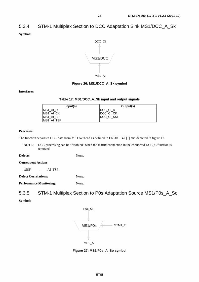
ETSI
ETSI EN 300 417-3-1 V1.2.1 (2001-10)36
5.3.4 STM-1 Multiplex Section to DCC Adaptation Sink MS1/DCC_A_Sk
Symbol:
MS1/DCC
DCC_CI
MS1_AI
Figure 26: MS1/DCC_A_Sk symbol
Interfaces:
Table 17: MS1/DCC_A_Sk input and output signals
Input(s) Output(s) MS1_AI_D MS1_AI_CK MS1_AI_FS MS1_AI_TSF
DCC_CI_D DCC_CI_CK DCC_CI_SSF
Processes:
The function separates DCC data from MS Overhead as defined in EN 300 147 [1] and depicted in figure 17.
NOTE: DCC processing can be "disabled" when the matrix connection in the connected DCC_C function is removed.
Defects: None.
Consequent Actions:
aSSF ← AI_TSF.
Defect Correlations: None.
Performance Monitoring: None.
5.3.5 STM-1 Multiplex Section to P0s Adaptation Source MS1/P0s_A_So
Symbol:
MS1/P0s
P0s_CI
MS1_AI
STM1_TI
Figure 27: MS1/P0s_A_So symbol
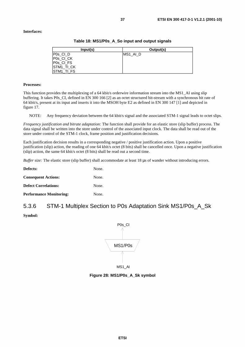
ETSI
ETSI EN 300 417-3-1 V1.2.1 (2001-10)37
Interfaces:
Table 18: MS1/P0s_A_So input and output signals
Input(s) Output(s) P0s_CI_D P0s_CI_CK P0s_CI_FS STM1_TI_CK STM1_TI_FS
MS1_AI_D
Processes:
This function provides the multiplexing of a 64 kbit/s orderwire information stream into the MS1_AI using slip buffering. It takes P0s_CI, defined in EN 300 166 [2] as an octet structured bit-stream with a synchronous bit rate of 64 kbit/s, present at its input and inserts it into the MSOH byte E2 as defined in EN 300 147 [1] and depicted in figure 17.
NOTE: Any frequency deviation between the 64 kbit/s signal and the associated STM-1 signal leads to octet slips.
Frequency justification and bitrate adaptation: The function shall provide for an elastic store (slip buffer) process. The data signal shall be written into the store under control of the associated input clock. The data shall be read out of the store under control of the STM-1 clock, frame position and justification decisions.
Each justification decision results in a corresponding negative / positive justification action. Upon a positive justification (slip) action, the reading of one 64 kbit/s octet (8 bits) shall be cancelled once. Upon a negative justification (slip) action, the same 64 kbit/s octet (8 bits) shall be read out a second time.
Buffer size: The elastic store (slip buffer) shall accommodate at least 18 µs of wander without introducing errors.
Defects: None.
Consequent Actions: None.
Defect Correlations: None.
Performance Monitoring: None.
5.3.6 STM-1 Multiplex Section to P0s Adaptation Sink MS1/P0s_A_Sk
Symbol:
MS1/P0s
P0s_CI
MS1_AI
Figure 28: MS1/P0s_A_Sk symbol
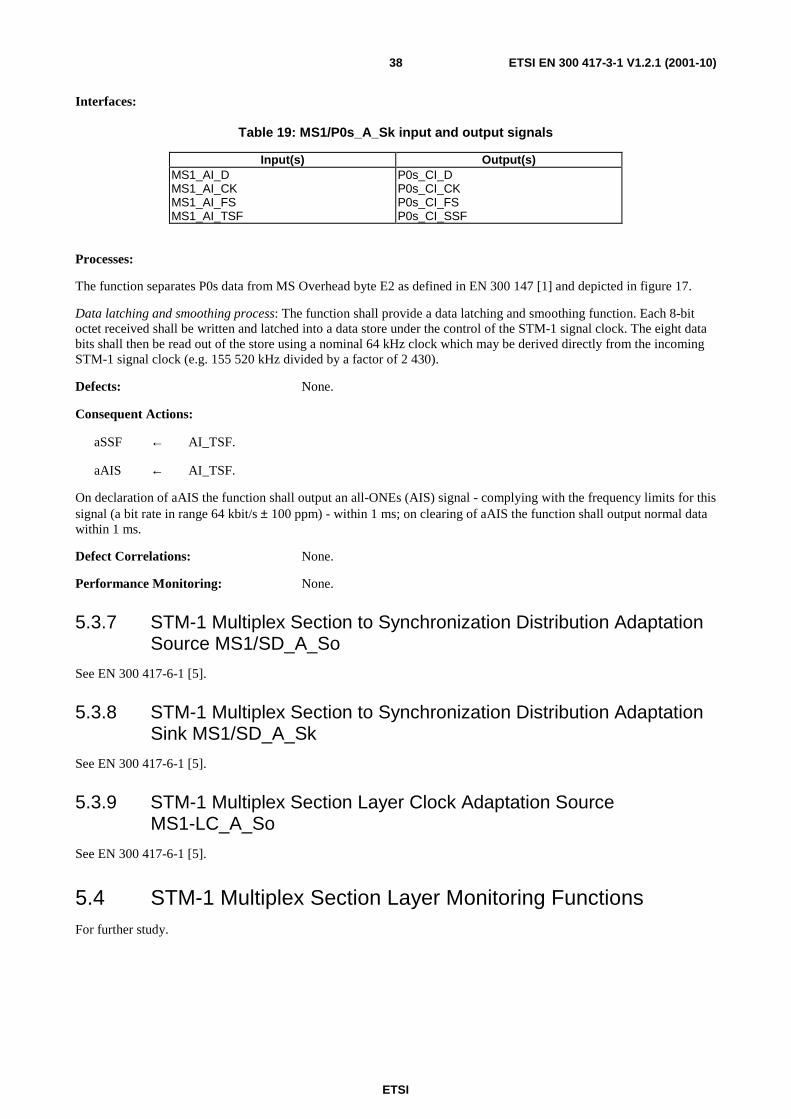
ETSI
ETSI EN 300 417-3-1 V1.2.1 (2001-10)38
Interfaces:
Table 19: MS1/P0s_A_Sk input and output signals
Input(s) Output(s) MS1_AI_D MS1_AI_CK MS1_AI_FS MS1_AI_TSF
P0s_CI_D P0s_CI_CK P0s_CI_FS P0s_CI_SSF
Processes:
The function separates P0s data from MS Overhead byte E2 as defined in EN 300 147 [1] and depicted in figure 17.
Data latching and smoothing process: The function shall provide a data latching and smoothing function. Each 8-bit octet received shall be written and latched into a data store under the control of the STM-1 signal clock. The eight data bits shall then be read out of the store using a nominal 64 kHz clock which may be derived directly from the incoming STM-1 signal clock (e.g. 155 520 kHz divided by a factor of 2 430).
Defects: None.
Consequent Actions:
aSSF ← AI_TSF.
aAIS ← AI_TSF.
On declaration of aAIS the function shall output an all-ONEs (AIS) signal - complying with the frequency limits for this signal (a bit rate in range 64 kbit/s ± 100 ppm) - within 1 ms; on clearing of aAIS the function shall output normal data within 1 ms.
Defect Correlations: None.
Performance Monitoring: None.
5.3.7 STM-1 Multiplex Section to Synchronization Distribution Adaptation Source MS1/SD_A_So
See EN 300 417-6-1 [5].
5.3.8 STM-1 Multiplex Section to Synchronization Distribution Adaptation Sink MS1/SD_A_Sk
See EN 300 417-6-1 [5].
5.3.9 STM-1 Multiplex Section Layer Clock Adaptation Source MS1-LC_A_So
See EN 300 417-6-1 [5].
5.4 STM-1 Multiplex Section Layer Monitoring Functions For further study.
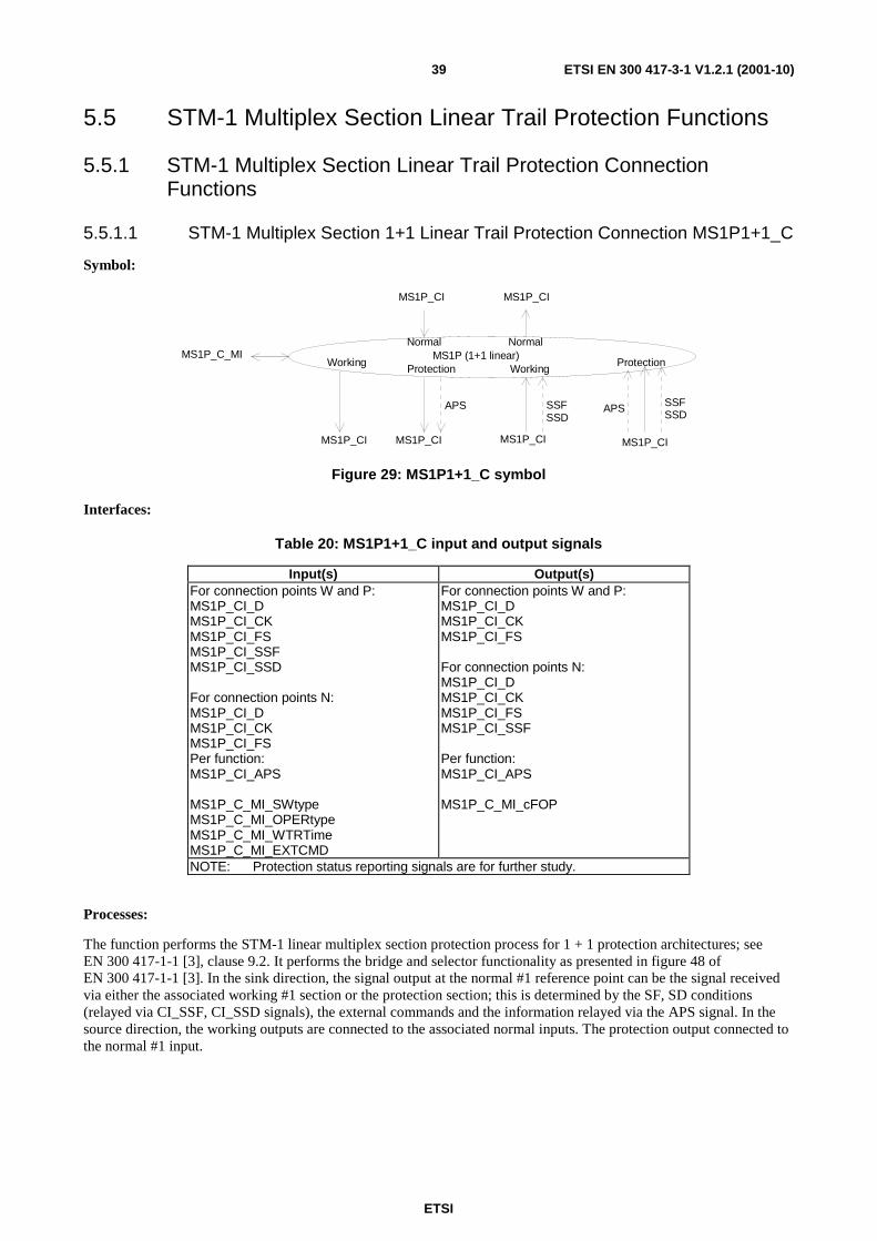
ETSI
ETSI EN 300 417-3-1 V1.2.1 (2001-10)39
5.5 STM-1 Multiplex Section Linear Trail Protection Functions
5.5.1 STM-1 Multiplex Section Linear Trail Protection Connection Functions
5.5.1.1 STM-1 Multiplex Section 1+1 Linear Trail Protection Connection MS1P1+1_C
Symbol:
MS1P_CI MS1P_CI
MS1P (1+1 linear)
APS SSFSSD
WorkingProtection Working
APS SSFSSD
Protection
MS1P_CI MS1P_CI
MS1P_CI MS1P_CI
Normal NormalMS1P_C_MI
Figure 29: MS1P1+1_C symbol
Interfaces:
Table 20: MS1P1+1_C input and output signals
Input(s) Output(s) For connection points W and P: MS1P_CI_D MS1P_CI_CK MS1P_CI_FS MS1P_CI_SSF MS1P_CI_SSD For connection points N: MS1P_CI_D MS1P_CI_CK MS1P_CI_FS Per function: MS1P_CI_APS MS1P_C_MI_SWtype MS1P_C_MI_OPERtype MS1P_C_MI_WTRTime MS1P_C_MI_EXTCMD
For connection points W and P: MS1P_CI_D MS1P_CI_CK MS1P_CI_FS For connection points N: MS1P_CI_D MS1P_CI_CK MS1P_CI_FS MS1P_CI_SSF Per function: MS1P_CI_APS MS1P_C_MI_cFOP
NOTE: Protection status reporting signals are for further study.
Processes:
The function performs the STM-1 linear multiplex section protection process for 1 + 1 protection architectures; see EN 300 417-1-1 [3], clause 9.2. It performs the bridge and selector functionality as presented in figure 48 of EN 300 417-1-1 [3]. In the sink direction, the signal output at the normal #1 reference point can be the signal received via either the associated working #1 section or the protection section; this is determined by the SF, SD conditions (relayed via CI_SSF, CI_SSD signals), the external commands and the information relayed via the APS signal. In the source direction, the working outputs are connected to the associated normal inputs. The protection output connected to the normal #1 input.
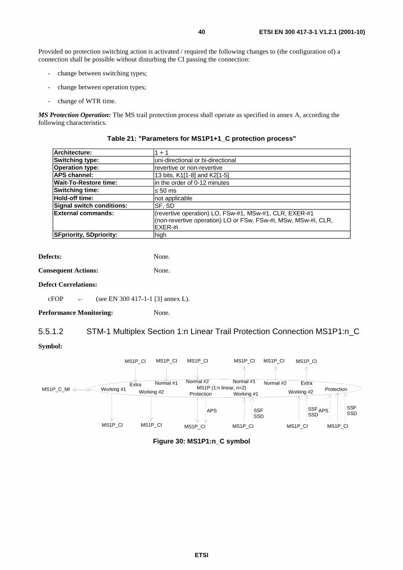
ETSI
ETSI EN 300 417-3-1 V1.2.1 (2001-10)40
Provided no protection switching action is activated / required the following changes to (the configuration of) a connection shall be possible without disturbing the CI passing the connection:
- change between switching types;
- change between operation types;
- change of WTR time.
MS Protection Operation: The MS trail protection process shall operate as specified in annex A, according the following characteristics.
Table 21: "Parameters for MS1P1+1_C protection process"
Architecture: 1 + 1 Switching type: uni-directional or bi-directional Operation type: revertive or non-revertive APS channel: 13 bits, K1[1-8] and K2[1-5] Wait-To-Restore time: in the order of 0-12 minutes Switching time: ≤ 50 ms Hold-off time: not applicable Signal switch conditions: SF, SD External commands: (revertive operation) LO, FSw-#1, MSw-#1, CLR, EXER-#1
(non-revertive operation) LO or FSw, FSw-#i, MSw, MSw-#i, CLR, EXER-#i
SFpriority, SDpriority: high
Defects: None.
Consequent Actions: None.
Defect Correlations:
cFOP ← (see EN 300 417-1-1 [3] annex L).
Performance Monitoring: None.
5.5.1.2 STM-1 Multiplex Section 1:n Linear Trail Protection Connection MS1P1:n_C
Symbol:
MS1P_CI MS1P_CI
MS1P (1:n linear, n=2)
APS SSFSSD
Working #1Protection Working #1
MS1P_CI
Working #2
SSFSSD
Working #2
APSSSFSSD
Protection
MS1P_CI MS1P_CI MS1P_CI
MS1P_CI MS1P_CI MS1P_CI MS1P_CI
MS1P_C_MINormal #1 Normal #2Normal #1Normal #2
MS1P_CI
ExtraExtra
MS1P_CI
Figure 30: MS1P1:n_C symbol
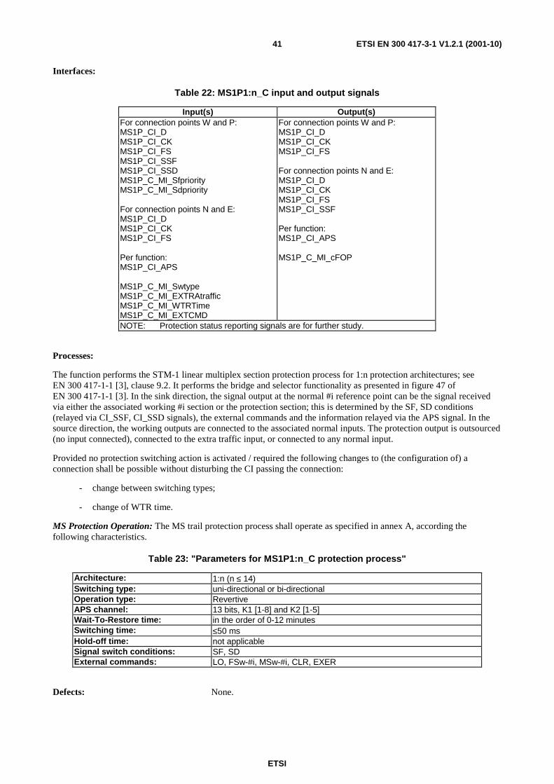
ETSI
ETSI EN 300 417-3-1 V1.2.1 (2001-10)41
Interfaces:
Table 22: MS1P1:n_C input and output signals
Input(s) Output(s) For connection points W and P: MS1P_CI_D MS1P_CI_CK MS1P_CI_FS MS1P_CI_SSF MS1P_CI_SSD MS1P_C_MI_Sfpriority MS1P_C_MI_Sdpriority For connection points N and E: MS1P_CI_D MS1P_CI_CK MS1P_CI_FS Per function: MS1P_CI_APS MS1P_C_MI_Swtype MS1P_C_MI_EXTRAtraffic MS1P_C_MI_WTRTime MS1P_C_MI_EXTCMD
For connection points W and P: MS1P_CI_D MS1P_CI_CK MS1P_CI_FS For connection points N and E: MS1P_CI_D MS1P_CI_CK MS1P_CI_FS MS1P_CI_SSF Per function: MS1P_CI_APS MS1P_C_MI_cFOP
NOTE: Protection status reporting signals are for further study.
Processes:
The function performs the STM-1 linear multiplex section protection process for 1:n protection architectures; see EN 300 417-1-1 [3], clause 9.2. It performs the bridge and selector functionality as presented in figure 47 of EN 300 417-1-1 [3]. In the sink direction, the signal output at the normal #i reference point can be the signal received via either the associated working #i section or the protection section; this is determined by the SF, SD conditions (relayed via CI_SSF, CI_SSD signals), the external commands and the information relayed via the APS signal. In the source direction, the working outputs are connected to the associated normal inputs. The protection output is outsourced (no input connected), connected to the extra traffic input, or connected to any normal input.
Provided no protection switching action is activated / required the following changes to (the configuration of) a connection shall be possible without disturbing the CI passing the connection:
- change between switching types;
- change of WTR time.
MS Protection Operation: The MS trail protection process shall operate as specified in annex A, according the following characteristics.
Table 23: "Parameters for MS1P1:n_C protection process"
Architecture: 1:n (n ≤ 14) Switching type: uni-directional or bi-directional Operation type: Revertive APS channel: 13 bits, K1 [1-8] and K2 [1-5] Wait-To-Restore time: in the order of 0-12 minutes Switching time: ≤50 ms Hold-off time: not applicable Signal switch conditions: SF, SD External commands: LO, FSw-#i, MSw-#i, CLR, EXER
Defects: None.
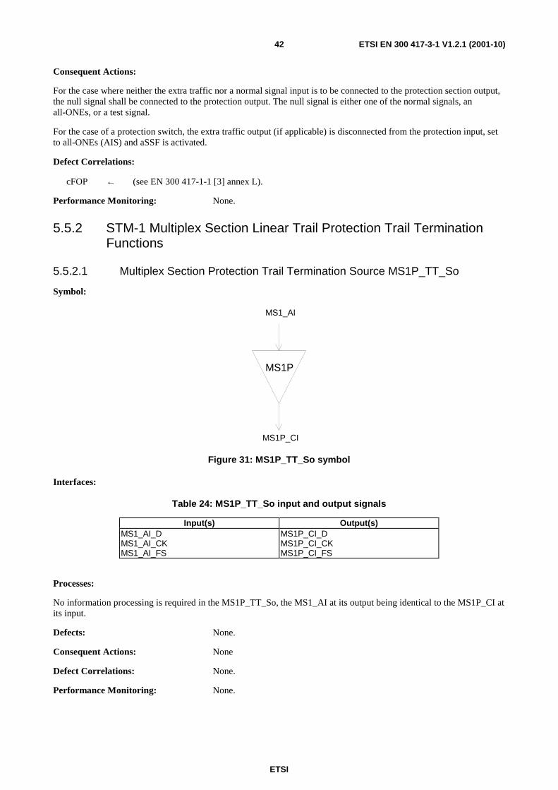
ETSI
ETSI EN 300 417-3-1 V1.2.1 (2001-10)42
Consequent Actions:
For the case where neither the extra traffic nor a normal signal input is to be connected to the protection section output, the null signal shall be connected to the protection output. The null signal is either one of the normal signals, an all-ONEs, or a test signal.
For the case of a protection switch, the extra traffic output (if applicable) is disconnected from the protection input, set to all-ONEs (AIS) and aSSF is activated.
Defect Correlations:
cFOP ← (see EN 300 417-1-1 [3] annex L).
Performance Monitoring: None.
5.5.2 STM-1 Multiplex Section Linear Trail Protection Trail Termination Functions
5.5.2.1 Multiplex Section Protection Trail Termination Source MS1P_TT_So
Symbol:
MS1P
MS1_AI
MS1P_CI
Figure 31: MS1P_TT_So symbol
Interfaces:
Table 24: MS1P_TT_So input and output signals
Input(s) Output(s) MS1_AI_D MS1_AI_CK MS1_AI_FS
MS1P_CI_D MS1P_CI_CK MS1P_CI_FS
Processes:
No information processing is required in the MS1P_TT_So, the MS1_AI at its output being identical to the MS1P_CI at its input.
Defects: None.
Consequent Actions: None
Defect Correlations: None.
Performance Monitoring: None.
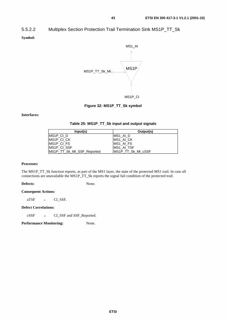
ETSI
ETSI EN 300 417-3-1 V1.2.1 (2001-10)43
5.5.2.2 Multiplex Section Protection Trail Termination Sink MS1P_TT_Sk
Symbol:
MS1P
MS1_AI
MS1P_CI
MS1P_TT_Sk_MI
Figure 32: MS1P_TT_Sk symbol
Interfaces:
Table 25: MS1P_TT_Sk input and output signals
Input(s) Output(s) MS1P_CI_D MS1P_CI_CK MS1P_CI_FS MS1P_CI_SSF MS1P_TT_Sk_MI_SSF_Reported
MS1_AI_D MS1_AI_CK MS1_AI_FS MS1_AI_TSF MS1P_TT_Sk_MI_cSSF
Processes:
The MS1P_TT_Sk function reports, as part of the MS1 layer, the state of the protected MS1 trail. In case all connections are unavailable the MS1P_TT_Sk reports the signal fail condition of the protected trail.
Defects: None.
Consequent Actions:
aTSF ← CI_SSF.
Defect Correlations:
cSSF ← CI_SSF and SSF_Reported.
Performance Monitoring: None.
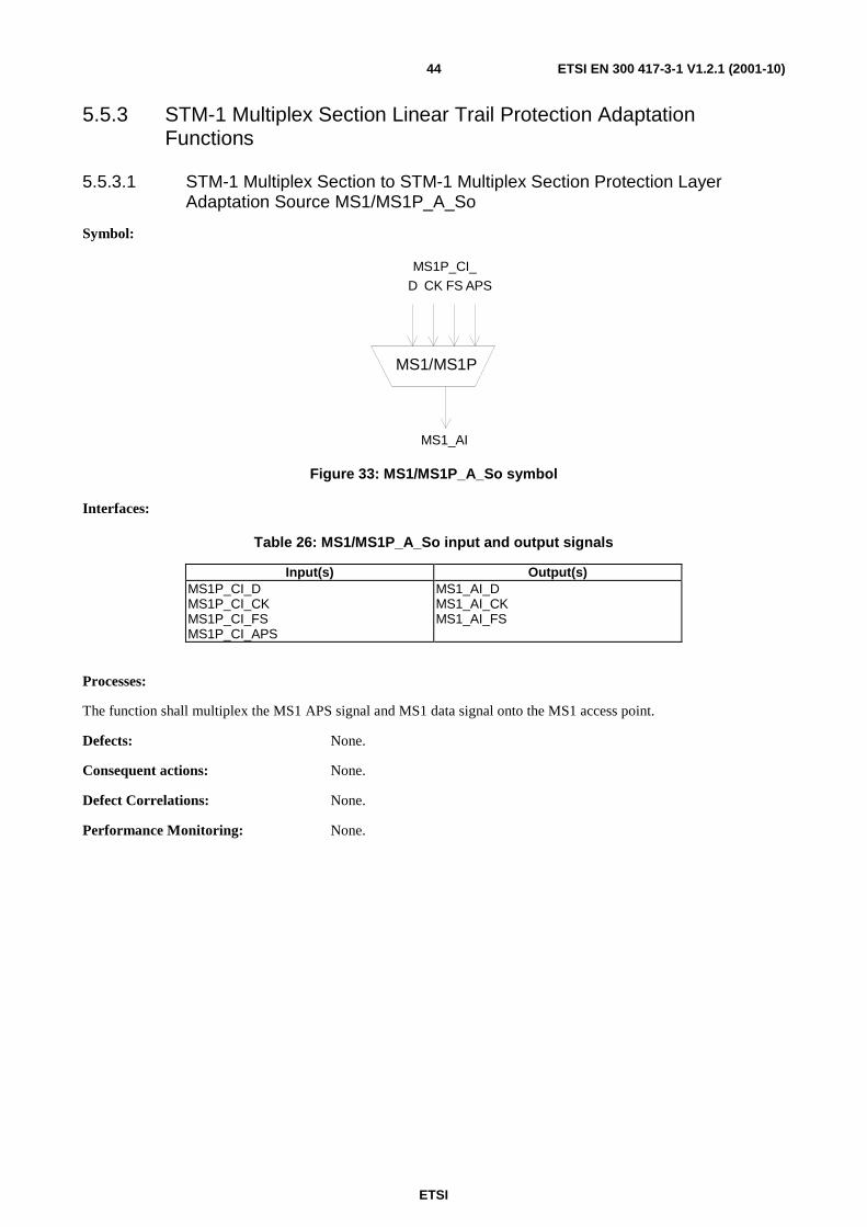
ETSI
ETSI EN 300 417-3-1 V1.2.1 (2001-10)44
5.5.3 STM-1 Multiplex Section Linear Trail Protection Adaptation Functions
5.5.3.1 STM-1 Multiplex Section to STM-1 Multiplex Section Protection Layer Adaptation Source MS1/MS1P_A_So
Symbol:
MS1/MS1P
MS1P_CI_
MS1_AI
D CK FS APS
Figure 33: MS1/MS1P_A_So symbol
Interfaces:
Table 26: MS1/MS1P_A_So input and output signals
Input(s) Output(s) MS1P_CI_D MS1P_CI_CK MS1P_CI_FS MS1P_CI_APS
MS1_AI_D MS1_AI_CK MS1_AI_FS
Processes:
The function shall multiplex the MS1 APS signal and MS1 data signal onto the MS1 access point.
Defects: None.
Consequent actions: None.
Defect Correlations: None.
Performance Monitoring: None.
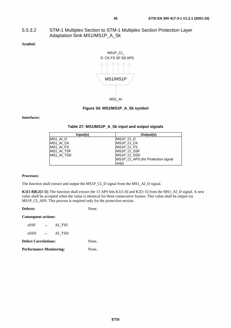
ETSI
ETSI EN 300 417-3-1 V1.2.1 (2001-10)45
5.5.3.2 STM-1 Multiplex Section to STM-1 Multiplex Section Protection Layer Adaptation Sink MS1/MS1P_A_Sk
Symbol:
MS1/MS1P
MS1P_CI_
MS1_AI
D CK FS SF SD APS
Figure 34: MS1/MS1P_A_Sk symbol
Interfaces:
Table 27: MS1/MS1P_A_Sk input and output signals
Input(s) Output(s) MS1_AI_D MS1_AI_CK MS1_AI_FS MS1_AI_TSF MS1_AI_TSD
MS1P_CI_D MS1P_CI_CK MS1P_CI_FS MS1P_CI_SSF MS1P_CI_SSD MS1P_CI_APS (for Protection signal only)
Processes:
The function shall extract and output the MS1P_CI_D signal from the MS1_AI_D signal.
K1[1-8]K2[1-5]: The function shall extract the 13 APS bits K1[1-8] and K2[1-5] from the MS1_AI_D signal. A new value shall be accepted when the value is identical for three consecutive frames. This value shall be output via MS1P_CI_APS. This process is required only for the protection section.
Defects: None.
Consequent actions:
aSSF ← AI_TSF.
aSSD ← AI_TSD.
Defect Correlations: None.
Performance Monitoring: None.
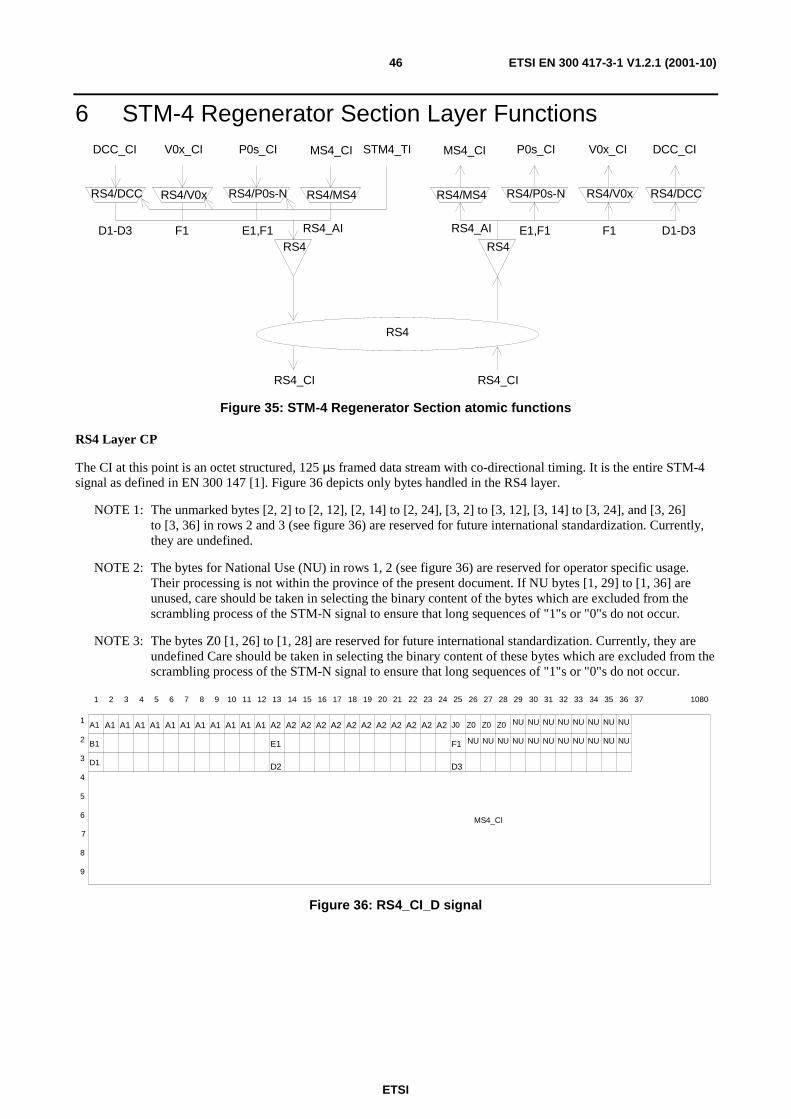
ETSI
ETSI EN 300 417-3-1 V1.2.1 (2001-10)46
6 STM-4 Regenerator Section Layer Functions
RS4
RS4/MS4
RS4
RS4/MS4
MS4_CI MS4_CI
RS4_CI RS4_CI
RS4/V0x RS4/V0xRS4/P0s-N
P0s_CISTM4_TI
RS4/P0s-N
P0s_CI
E1,F1 E1,F1
V0x_CIV0x_CI
RS4/DCC
DCC_CI
F1 D1-D3
RS4/DCC
DCC_CI
D1-D3 F1 RS4_AI RS4_AI
RS4
Figure 35: STM-4 Regenerator Section atomic functions
RS4 Layer CP
The CI at this point is an octet structured, 125 µs framed data stream with co-directional timing. It is the entire STM-4 signal as defined in EN 300 147 [1]. Figure 36 depicts only bytes handled in the RS4 layer.
NOTE 1: The unmarked bytes [2, 2] to [2, 12], [2, 14] to [2, 24], [3, 2] to [3, 12], [3, 14] to [3, 24], and [3, 26] to [3, 36] in rows 2 and 3 (see figure 36) are reserved for future international standardization. Currently, they are undefined.
NOTE 2: The bytes for National Use (NU) in rows 1, 2 (see figure 36) are reserved for operator specific usage. Their processing is not within the province of the present document. If NU bytes [1, 29] to [1, 36] are unused, care should be taken in selecting the binary content of the bytes which are excluded from the scrambling process of the STM-N signal to ensure that long sequences of "1"s or "0"s do not occur.
NOTE 3: The bytes Z0 [1, 26] to [1, 28] are reserved for future international standardization. Currently, they are undefined Care should be taken in selecting the binary content of these bytes which are excluded from the scrambling process of the STM-N signal to ensure that long sequences of "1"s or "0"s do not occur.
A1 A1
B1
D1
A1 A1 A1 A1 A2 A2
E1
D2
A2 A2 A2 A2 J0 Z0
F1
D3
Z0 Z0A2 A2A2A2A2A2A1A1A1A1A1A11
2
3
4
5
6
7
8
9
NU NU NU NU NU NU NU NU
NU NU NU NU NU NU NU NU NU NU NU
1 2 3 4 5 6 7 8 9 10 11 12 13 14 15 16 17 18 19 20 21 22 23 24 25 26 27 28 29 30 31 32 33 34 35 36 37 1080
MS4_CI
Figure 36: RS4_CI_D signal
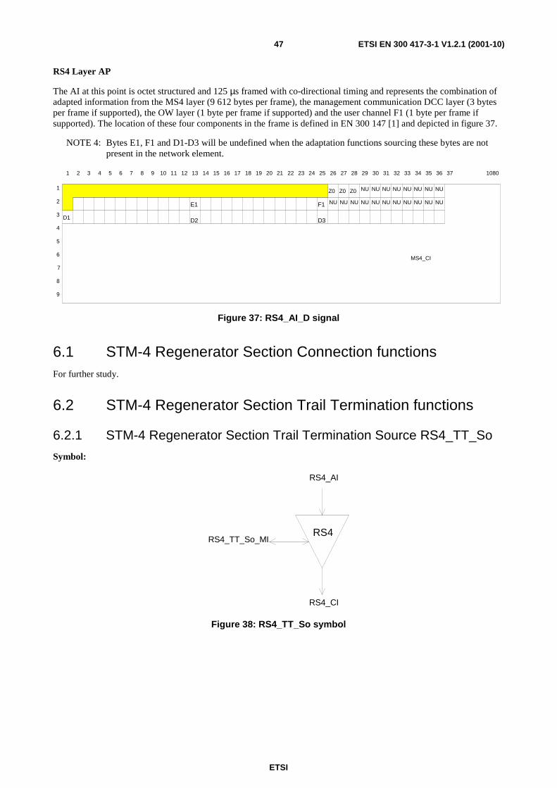
ETSI
ETSI EN 300 417-3-1 V1.2.1 (2001-10)47
RS4 Layer AP
The AI at this point is octet structured and 125 µs framed with co-directional timing and represents the combination of adapted information from the MS4 layer (9 612 bytes per frame), the management communication DCC layer (3 bytes per frame if supported), the OW layer (1 byte per frame if supported) and the user channel F1 (1 byte per frame if supported). The location of these four components in the frame is defined in EN 300 147 [1] and depicted in figure 37.
NOTE 4: Bytes E1, F1 and D1-D3 will be undefined when the adaptation functions sourcing these bytes are not present in the network element.
D1
E1
D2
Z0
F1
D3
Z0 Z01
2
3
4
5
6
7
8
9
NU NU NU NU NU NU NU NU
NU NU NU NU NU NU NU NU NU NU NU
1 2 3 4 5 6 7 8 9 10 11 12 13 14 15 16 17 18 19 20 21 22 23 24 25 26 27 28 29 30 31 32 33 34 35 36 37 1080
MS4_CI
Figure 37: RS4_AI_D signal
6.1 STM-4 Regenerator Section Connection functions For further study.
6.2 STM-4 Regenerator Section Trail Termination functions
6.2.1 STM-4 Regenerator Section Trail Termination Source RS4_TT_So
Symbol:
RS4
RS4_AI
RS4_CI
RS4_TT_So_MI
Figure 38: RS4_TT_So symbol
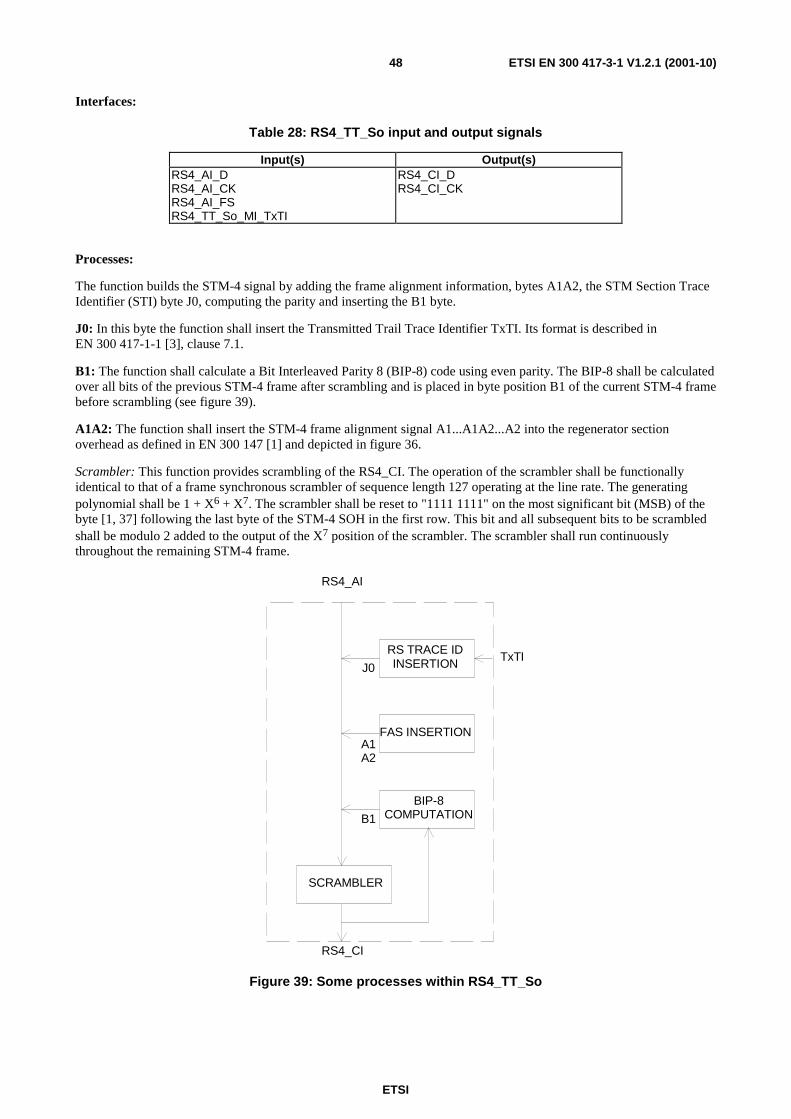
ETSI
ETSI EN 300 417-3-1 V1.2.1 (2001-10)48
Interfaces:
Table 28: RS4_TT_So input and output signals
Input(s) Output(s) RS4_AI_D RS4_AI_CK RS4_AI_FS RS4_TT_So_MI_TxTI
RS4_CI_D RS4_CI_CK
Processes:
The function builds the STM-4 signal by adding the frame alignment information, bytes A1A2, the STM Section Trace Identifier (STI) byte J0, computing the parity and inserting the B1 byte.
J0: In this byte the function shall insert the Transmitted Trail Trace Identifier TxTI. Its format is described in EN 300 417-1-1 [3], clause 7.1.
B1: The function shall calculate a Bit Interleaved Parity 8 (BIP-8) code using even parity. The BIP-8 shall be calculated over all bits of the previous STM-4 frame after scrambling and is placed in byte position B1 of the current STM-4 frame before scrambling (see figure 39).
A1A2: The function shall insert the STM-4 frame alignment signal A1...A1A2...A2 into the regenerator section overhead as defined in EN 300 147 [1] and depicted in figure 36.
Scrambler: This function provides scrambling of the RS4_CI. The operation of the scrambler shall be functionally identical to that of a frame synchronous scrambler of sequence length 127 operating at the line rate. The generating polynomial shall be 1 + X6 + X7. The scrambler shall be reset to "1111 1111" on the most significant bit (MSB) of the byte [1, 37] following the last byte of the STM-4 SOH in the first row. This bit and all subsequent bits to be scrambled shall be modulo 2 added to the output of the X7 position of the scrambler. The scrambler shall run continuously throughout the remaining STM-4 frame.
SCRAMBLER
BIP-8COMPUTATIONB1
RS4_CI
RS TRACE IDINSERTIONJ0
FAS INSERTION
RS4_AI
A1A2
TxTI
Figure 39: Some processes within RS4_TT_So
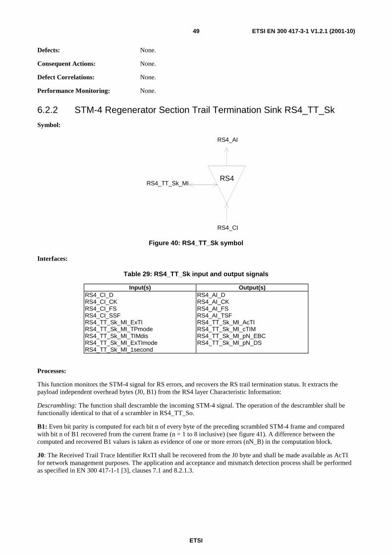
ETSI
ETSI EN 300 417-3-1 V1.2.1 (2001-10)49
Defects: None.
Consequent Actions: None.
Defect Correlations: None.
Performance Monitoring: None.
6.2.2 STM-4 Regenerator Section Trail Termination Sink RS4_TT_Sk
Symbol:
RS4
RS4_AI
RS4_CI
RS4_TT_Sk_MI
Figure 40: RS4_TT_Sk symbol
Interfaces:
Table 29: RS4_TT_Sk input and output signals
Input(s) Output(s) RS4_CI_D RS4_CI_CK RS4_CI_FS RS4_CI_SSF RS4_TT_Sk_MI_ExTI RS4_TT_Sk_MI_TPmode RS4_TT_Sk_MI_TIMdis RS4_TT_Sk_MI_ExTImode RS4_TT_Sk_MI_1second
RS4_AI_D RS4_AI_CK RS4_AI_FS RS4_AI_TSF RS4_TT_Sk_MI_AcTI RS4_TT_Sk_MI_cTIM RS4_TT_Sk_MI_pN_EBC RS4_TT_Sk_MI_pN_DS
Processes:
This function monitors the STM-4 signal for RS errors, and recovers the RS trail termination status. It extracts the payload independent overhead bytes (J0, B1) from the RS4 layer Characteristic Information:
Descrambling: The function shall descramble the incoming STM-4 signal. The operation of the descrambler shall be functionally identical to that of a scrambler in RS4_TT_So.
B1: Even bit parity is computed for each bit n of every byte of the preceding scrambled STM-4 frame and compared with bit n of B1 recovered from the current frame (n = 1 to 8 inclusive) (see figure 41). A difference between the computed and recovered B1 values is taken as evidence of one or more errors (nN_B) in the computation block.
J0: The Received Trail Trace Identifier RxTI shall be recovered from the J0 byte and shall be made available as AcTI for network management purposes. The application and acceptance and mismatch detection process shall be performed as specified in EN 300 417-1-1 [3], clauses 7.1 and 8.2.1.3.
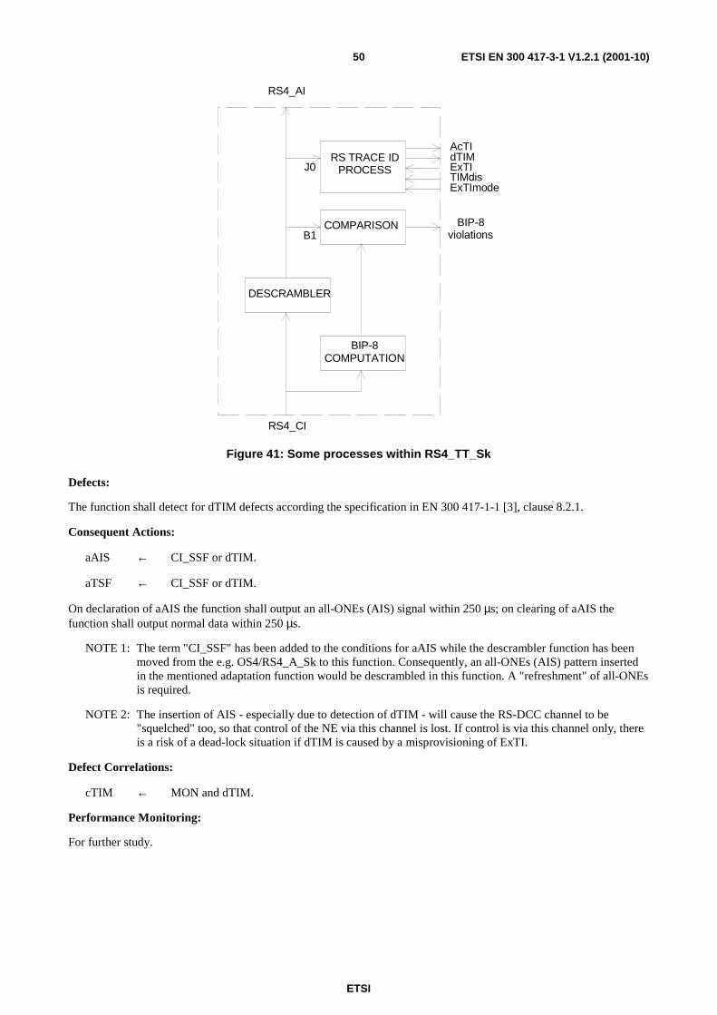
ETSI
ETSI EN 300 417-3-1 V1.2.1 (2001-10)50
DESCRAMBLER
BIP-8COMPUTATION
B1
RS TRACE IDPROCESSJ0
RS4_CI
COMPARISON BIP-8violations
AcTIdTIMExTI
RS4_AI
TIMdisExTImode
Figure 41: Some processes within RS4_TT_Sk
Defects:
The function shall detect for dTIM defects according the specification in EN 300 417-1-1 [3], clause 8.2.1.
Consequent Actions:
aAIS ← CI_SSF or dTIM.
aTSF ← CI_SSF or dTIM.
On declaration of aAIS the function shall output an all-ONEs (AIS) signal within 250 µs; on clearing of aAIS the function shall output normal data within 250 µs.
NOTE 1: The term "CI_SSF" has been added to the conditions for aAIS while the descrambler function has been moved from the e.g. OS4/RS4_A_Sk to this function. Consequently, an all-ONEs (AIS) pattern inserted in the mentioned adaptation function would be descrambled in this function. A "refreshment" of all-ONEs is required.
NOTE 2: The insertion of AIS - especially due to detection of dTIM - will cause the RS-DCC channel to be "squelched" too, so that control of the NE via this channel is lost. If control is via this channel only, there is a risk of a dead-lock situation if dTIM is caused by a misprovisioning of ExTI.
Defect Correlations:
cTIM ← MON and dTIM.
Performance Monitoring:
For further study.
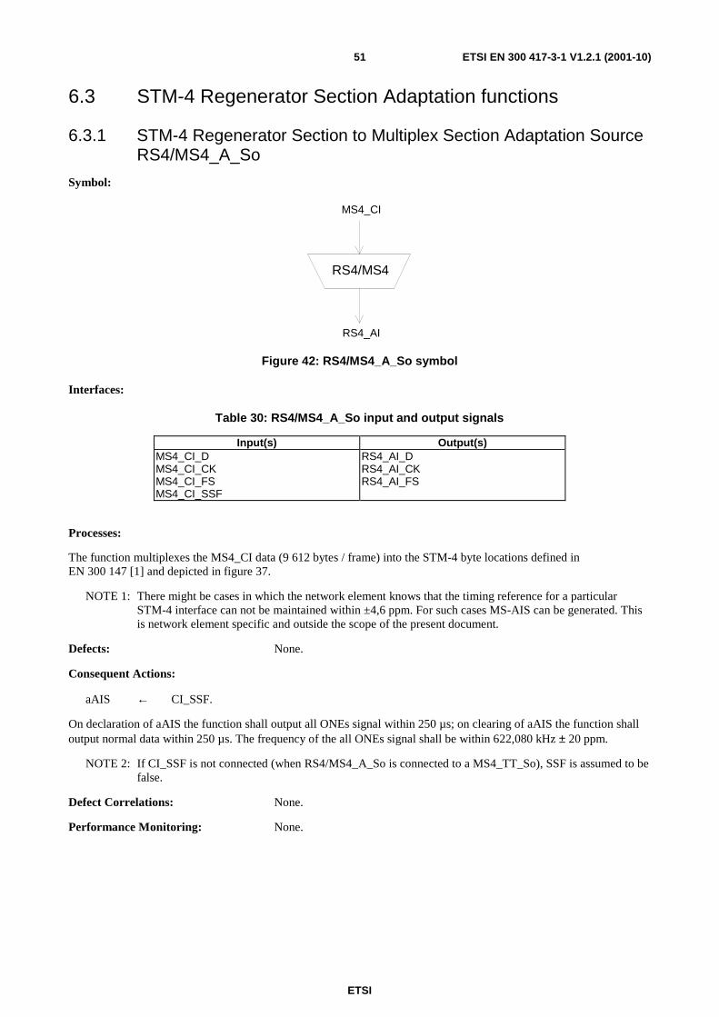
ETSI
ETSI EN 300 417-3-1 V1.2.1 (2001-10)51
6.3 STM-4 Regenerator Section Adaptation functions
6.3.1 STM-4 Regenerator Section to Multiplex Section Adaptation Source RS4/MS4_A_So
Symbol:
RS4/MS4
MS4_CI
RS4_AI
Figure 42: RS4/MS4_A_So symbol
Interfaces:
Table 30: RS4/MS4_A_So input and output signals
Input(s) Output(s) MS4_CI_D MS4_CI_CK MS4_CI_FS MS4_CI_SSF
RS4_AI_D RS4_AI_CK RS4_AI_FS
Processes:
The function multiplexes the MS4_CI data (9 612 bytes / frame) into the STM-4 byte locations defined in EN 300 147 [1] and depicted in figure 37.
NOTE 1: There might be cases in which the network element knows that the timing reference for a particular STM-4 interface can not be maintained within ±4,6 ppm. For such cases MS-AIS can be generated. This is network element specific and outside the scope of the present document.
Defects: None.
Consequent Actions:
aAIS ← CI_SSF.
On declaration of aAIS the function shall output all ONEs signal within 250 µs; on clearing of aAIS the function shall output normal data within 250 µs. The frequency of the all ONEs signal shall be within 622,080 kHz ± 20 ppm.
NOTE 2: If CI_SSF is not connected (when RS4/MS4_A_So is connected to a MS4_TT_So), SSF is assumed to be false.
Defect Correlations: None.
Performance Monitoring: None.
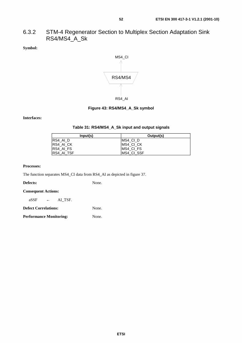
ETSI
ETSI EN 300 417-3-1 V1.2.1 (2001-10)52
6.3.2 STM-4 Regenerator Section to Multiplex Section Adaptation Sink RS4/MS4_A_Sk
Symbol:
RS4/MS4
MS4_CI
RS4_AI
Figure 43: RS4/MS4_A_Sk symbol
Interfaces:
Table 31: RS4/MS4_A_Sk input and output signals
Input(s) Output(s) RS4_AI_D RS4_AI_CK RS4_AI_FS RS4_AI_TSF
MS4_CI_D MS4_CI_CK MS4_CI_FS MS4_CI_SSF
Processes:
The function separates MS4_CI data from RS4_AI as depicted in figure 37.
Defects: None.
Consequent Actions:
aSSF ← AI_TSF.
Defect Correlations: None.
Performance Monitoring: None.
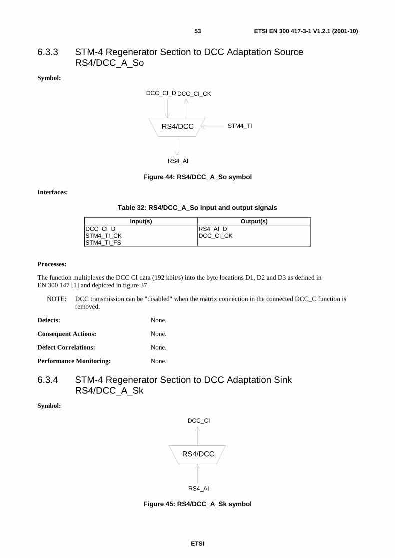
ETSI
ETSI EN 300 417-3-1 V1.2.1 (2001-10)53
6.3.3 STM-4 Regenerator Section to DCC Adaptation Source RS4/DCC_A_So
Symbol:
RS4/DCC
DCC_CI_D
RS4_AI
STM4_TI
DCC_CI_CK
Figure 44: RS4/DCC_A_So symbol
Interfaces:
Table 32: RS4/DCC_A_So input and output signals
Input(s) Output(s) DCC_CI_D STM4_TI_CK STM4_TI_FS
RS4_AI_D DCC_CI_CK
Processes:
The function multiplexes the DCC CI data (192 kbit/s) into the byte locations D1, D2 and D3 as defined in EN 300 147 [1] and depicted in figure 37.
NOTE: DCC transmission can be "disabled" when the matrix connection in the connected DCC_C function is removed.
Defects: None.
Consequent Actions: None.
Defect Correlations: None.
Performance Monitoring: None.
6.3.4 STM-4 Regenerator Section to DCC Adaptation Sink RS4/DCC_A_Sk
Symbol:
RS4/DCC
DCC_CI
RS4_AI
Figure 45: RS4/DCC_A_Sk symbol
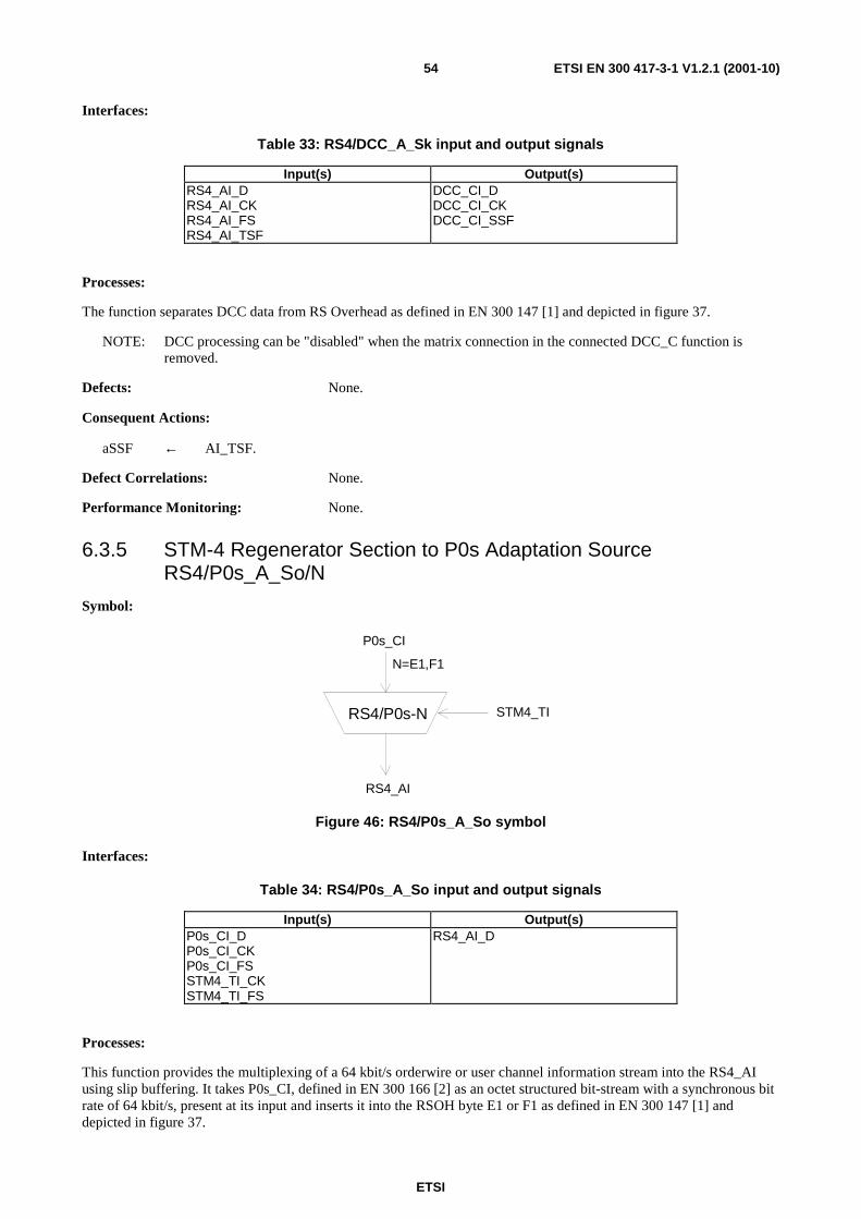
ETSI
ETSI EN 300 417-3-1 V1.2.1 (2001-10)54
Interfaces:
Table 33: RS4/DCC_A_Sk input and output signals
Input(s) Output(s) RS4_AI_D RS4_AI_CK RS4_AI_FS RS4_AI_TSF
DCC_CI_D DCC_CI_CK DCC_CI_SSF
Processes:
The function separates DCC data from RS Overhead as defined in EN 300 147 [1] and depicted in figure 37.
NOTE: DCC processing can be "disabled" when the matrix connection in the connected DCC_C function is removed.
Defects: None.
Consequent Actions:
aSSF ← AI_TSF.
Defect Correlations: None.
Performance Monitoring: None.
6.3.5 STM-4 Regenerator Section to P0s Adaptation Source RS4/P0s_A_So/N
Symbol:
RS4/P0s-N
P0s_CI
RS4_AI
STM4_TI
N=E1,F1
Figure 46: RS4/P0s_A_So symbol
Interfaces:
Table 34: RS4/P0s_A_So input and output signals
Input(s) Output(s) P0s_CI_D P0s_CI_CK P0s_CI_FS STM4_TI_CK STM4_TI_FS
RS4_AI_D
Processes:
This function provides the multiplexing of a 64 kbit/s orderwire or user channel information stream into the RS4_AI using slip buffering. It takes P0s_CI, defined in EN 300 166 [2] as an octet structured bit-stream with a synchronous bit rate of 64 kbit/s, present at its input and inserts it into the RSOH byte E1 or F1 as defined in EN 300 147 [1] and depicted in figure 37.
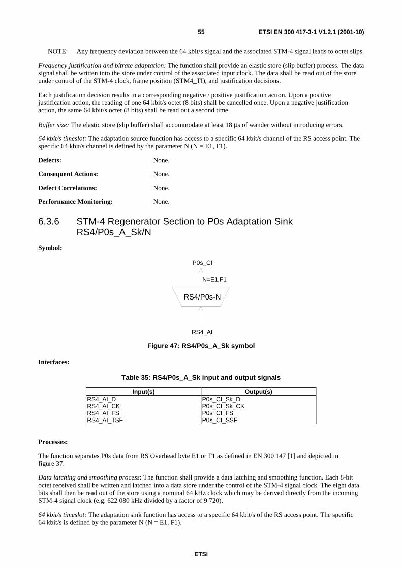
ETSI
ETSI EN 300 417-3-1 V1.2.1 (2001-10)55
NOTE: Any frequency deviation between the 64 kbit/s signal and the associated STM-4 signal leads to octet slips.
Frequency justification and bitrate adaptation: The function shall provide an elastic store (slip buffer) process. The data signal shall be written into the store under control of the associated input clock. The data shall be read out of the store under control of the STM-4 clock, frame position (STM4_TI), and justification decisions.
Each justification decision results in a corresponding negative / positive justification action. Upon a positive justification action, the reading of one 64 kbit/s octet (8 bits) shall be cancelled once. Upon a negative justification action, the same 64 kbit/s octet (8 bits) shall be read out a second time.
Buffer size: The elastic store (slip buffer) shall accommodate at least 18 µs of wander without introducing errors.
64 kbit/s timeslot: The adaptation source function has access to a specific 64 kbit/s channel of the RS access point. The specific 64 kbit/s channel is defined by the parameter N (N = E1, F1).
Defects: None.
Consequent Actions: None.
Defect Correlations: None.
Performance Monitoring: None.
6.3.6 STM-4 Regenerator Section to P0s Adaptation Sink RS4/P0s_A_Sk/N
Symbol:
RS4/P0s-N
P0s_CI
RS4_AI
N=E1,F1
Figure 47: RS4/P0s_A_Sk symbol
Interfaces:
Table 35: RS4/P0s_A_Sk input and output signals
Input(s) Output(s) RS4_AI_D RS4_AI_CK RS4_AI_FS RS4_AI_TSF
P0s_CI_Sk_D P0s_CI_Sk_CK P0s_CI_FS P0s_CI_SSF
Processes:
The function separates P0s data from RS Overhead byte E1 or F1 as defined in EN 300 147 [1] and depicted in figure 37.
Data latching and smoothing process: The function shall provide a data latching and smoothing function. Each 8-bit octet received shall be written and latched into a data store under the control of the STM-4 signal clock. The eight data bits shall then be read out of the store using a nominal 64 kHz clock which may be derived directly from the incoming STM-4 signal clock (e.g. 622 080 kHz divided by a factor of 9 720).
64 kbit/s timeslot: The adaptation sink function has access to a specific 64 kbit/s of the RS access point. The specific 64 kbit/s is defined by the parameter N (N = E1, F1).
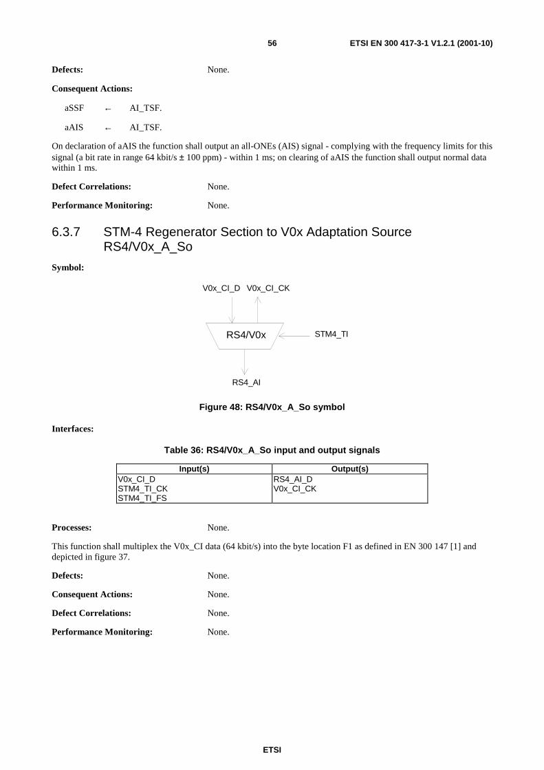
ETSI
ETSI EN 300 417-3-1 V1.2.1 (2001-10)56
Defects: None.
Consequent Actions:
aSSF ← AI_TSF.
aAIS ← AI_TSF.
On declaration of aAIS the function shall output an all-ONEs (AIS) signal - complying with the frequency limits for this signal (a bit rate in range 64 kbit/s ± 100 ppm) - within 1 ms; on clearing of aAIS the function shall output normal data within 1 ms.
Defect Correlations: None.
Performance Monitoring: None.
6.3.7 STM-4 Regenerator Section to V0x Adaptation Source RS4/V0x_A_So
Symbol:
RS4/V0x
RS4_AI
STM4_TI
V0x_CI_D V0x_CI_CK
Figure 48: RS4/V0x_A_So symbol
Interfaces:
Table 36: RS4/V0x_A_So input and output signals
Input(s) Output(s) V0x_CI_D STM4_TI_CK STM4_TI_FS
RS4_AI_D V0x_CI_CK
Processes: None.
This function shall multiplex the V0x_CI data (64 kbit/s) into the byte location F1 as defined in EN 300 147 [1] and depicted in figure 37.
Defects: None.
Consequent Actions: None.
Defect Correlations: None.
Performance Monitoring: None.
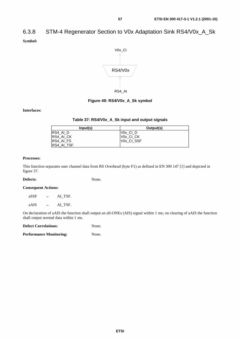
ETSI
ETSI EN 300 417-3-1 V1.2.1 (2001-10)57
6.3.8 STM-4 Regenerator Section to V0x Adaptation Sink RS4/V0x_A_Sk
Symbol:
RS4/V0x
V0x_CI
RS4_AI
Figure 49: RS4/V0x_A_Sk symbol
Interfaces:
Table 37: RS4/V0x_A_Sk input and output signals
Input(s) Output(s) RS4_AI_D RS4_AI_CK RS4_AI_FS RS4_AI_TSF
V0x_CI_D V0x_CI_CK V0x_CI_SSF
Processes:
This function separates user channel data from RS Overhead (byte F1) as defined in EN 300 147 [1] and depicted in figure 37.
Defects: None.
Consequent Actions:
aSSF ← AI_TSF.
aAIS ← AI_TSF.
On declaration of aAIS the function shall output an all-ONEs (AIS) signal within 1 ms; on clearing of aAIS the function shall output normal data within 1 ms.
Defect Correlations: None.
Performance Monitoring: None.
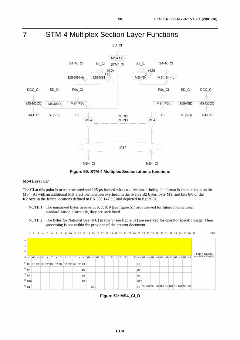
ETSI
ETSI EN 300 417-3-1 V1.2.1 (2001-10)58
7 STM-4 Multiplex Section Layer Functions
MS4
MS4/S4
MS4
S4_CI
MS4_CI MS4_CI
MS4/SD MS4/SDMS4/P0s
P0s_CI
STM4_TI
MS4/P0s
P0s_CI
E2 E2
SD_CISD_CI
MS4/DCC
DCC_CI
S1[5-8] D4-D12
MS4/DCC
DCC_CI
D4-D12 S1[5-8] RI_RDIRI_REI
MS4/S4-4c
S4-4c_CI
(1,0)(4,0)
MS4/S4
S4_CI
MS4/S4-4c
S4-4c_CI
(1,0)(4,0)
MS4-LC
SD_CI
MS4
Figure 50: STM-4 Multiplex Section atomic functions
MS4 Layer CP
The CI at this point is octet structured and 125 µs framed with co-directional timing. Its format is characterized as the MS4_AI with an additional MS Trail Termination overhead in the twelve B2 bytes, byte M1, and bits 6-8 of the K2 byte in the frame locations defined in EN 300 147 [1] and depicted in figure 51.
NOTE 1: The unmarked bytes in rows 5, 6, 7, 8, 9 (see figure 51) are reserved for future international standardization. Currently, they are undefined.
NOTE 2: The bytes for National Use (NU) in row 9 (see figure 51) are reserved for operator specific usage. Their processing is not within the province of the present document.
B2 B2
D4
D7
D10
S1
B2 B2 B2 B2 K1
D5
D8
D11
M1
K2
D6
D9
D12
E2
B2B2B2B2 B2 B2
1
2
3
4
5
6
7
8
9
H1 H1 H1 H1 H2 H2 H2 H2 H3 H3 H3 H3 H3 H3 H3 H3 H3 H3 H3 H3
NU NU NU NU NU NU NU NU NU NU NU
'1' '1' '1' '1' '1' '1' '1' '1'Y Y Y Y Y Y Y Y
1 2 3 4 5 6 7 8 9 10 11 12 13 14 15 16 17 18 19 20 21 22 23 24 25 26 27 28 29 30 31 32 33 34 35 36 37 1080
STM-4 payload(4 x 261 x 9 bytes)
Figure 51: MS4_CI_D
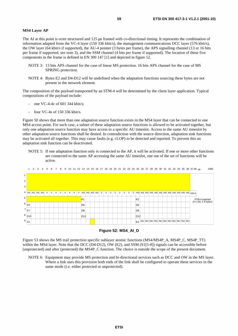
ETSI
ETSI EN 300 417-3-1 V1.2.1 (2001-10)59
MS4 Layer AP
The AI at this point is octet structured and 125 µs framed with co-directional timing. It represents the combination of information adapted from the VC-4 layer (150 336 kbit/s), the management communications DCC layer (576 kbit/s), the OW layer (64 kbit/s if supported), the AU-4 pointer (3 bytes per frame), the APS signalling channel (13 or 16 bits per frame if supported, see note 3), and the SSM channel (4 bits per frame if supported). The location of these five components in the frame is defined in EN 300 147 [1] and depicted in figure 52.
NOTE 3: 13 bits APS channel for the case of linear MS protection. 16 bits APS channel for the case of MS SPRING protection.
NOTE 4: Bytes E2 and D4-D12 will be undefined when the adaptation functions sourcing these bytes are not present in the network element.
The composition of the payload transported by an STM-4 will be determined by the client layer application. Typical compositions of the payload include:
- one VC-4-4c of 601 344 kbit/s;
- four VC-4s of 150 336 kbit/s.
Figure 50 shows that more than one adaptation source function exists in the MS4 layer that can be connected to one MS4 access point. For such case, a subset of these adaptation source functions is allowed to be activated together, but only one adaptation source function may have access to a specific AU timeslot. Access to the same AU timeslot by other adaptation source functions shall be denied. In contradiction with the source direction, adaptation sink functions may be activated all together. This may cause faults (e.g. cLOP) to be detected and reported. To prevent this an adaptation sink function can be deactivated.
NOTE 5: If one adaptation function only is connected to the AP, it will be activated. If one or more other functions are connected to the same AP accessing the same AU timeslot, one out of the set of functions will be active.
D4
D7
D10
S1
K1
D5
D8
D11
K2
D6
D9
D12
E2
1
2
3
4
5
6
7
8
9
H1 H1 H1 H1 H2 H2 H2 H2 H3 H3 H3 H3 H3 H3 H3 H3 H3 H3 H3 H3
NU NU NU NU NU NU NU NU NU NU NU
'1' '1' '1' '1' '1' '1' '1' '1'Y Y Y Y Y Y Y Y
1 2 3 4 5 6 7 8 9 10 11 12 13 14 15 16 17 18 19 20 21 22 23 24 25 26 27 28 29 30 31 32 33 34 35 36 37-48 1080
STM-4 payload(4 x 261 x 9 bytes)
49
H3+1
Figure 52: MS4_AI_D
Figure 53 shows the MS trail protection specific sublayer atomic functions (MS4/MS4P_A, MS4P_C, MS4P_TT) within the MS4 layer. Note that the DCC (D4-D12), OW (E2), and SSM (S1[5-8]) signals can be accessible before (unprotected) and after (protected) the MS4P_C function. The choice is outside the scope of the present document.
NOTE 6: Equipment may provide MS protection and bi-directional services such as DCC and OW in the MS layer. Where a link uses this provision both ends of the link shall be configured to operate these services in the same mode (i.e. either protected or unprotected).
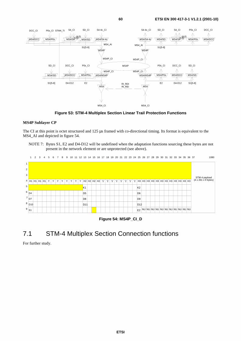
ETSI
ETSI EN 300 417-3-1 V1.2.1 (2001-10)60
MS4
MS4/MS4P
MS4
MS4/MS4P
MS4P
MS4_CI MS4_CI
MS4/P0s
P0s_CI
STM4_TI
MS4/P0s
P0s_CI
E2 E2
MS4/DCC
DCC_CI
D4-D12
MS4/DCC
DCC_CI
D4-D12 RI_RDIRI_REI
MS4/S4-4c
S4-4c_CI
MS4/S4-4c
S4-4c_CI
MS4/SD
SD_CI
S1[5-8]
MS4/SD
SD_CI
S1[5-8]MS4P MS4P
S4_CI
MS4/S4(1,0)(4,0)
S4_CI
MS4/S4(1,0)(4,0)
MS4/P0sMS4/DCC
P0s_CIDCC_CI
MS4/P0s MS4/DCC
P0s_CI DCC_CI
MS4/SD
SD_CI
S1[5-8]
MS4/SD
SD_CI
S1[5-8]
MS4_AI MS4_AI
MS4P_CI MS4P_CI
MS4P_CI MS4P_CI
Figure 53: STM-4 Multiplex Section Linear Trail Protection Functions
MS4P Sublayer CP
The CI at this point is octet structured and 125 µs framed with co-directional timing. Its format is equivalent to the MS4_AI and depicted in figure 54.
NOTE 7: Bytes S1, E2 and D4-D12 will be undefined when the adaptation functions sourcing these bytes are not present in the network element or are unprotected (see above).
D4
D7
D10
S1
K1
D5
D8
D11
K2
D6
D9
D12
E2
1
2
3
4
5
6
7
8
9
H1 H1 H1 H1 H2 H2 H2 H2 H3 H3 H3 H3 H3 H3 H3 H3 H3 H3 H3 H3
NU NU NU NU NU NU NU NU NU NU NU
'1' '1' '1' '1' '1' '1' '1' '1'Y Y Y Y Y Y Y Y
1 2 3 4 5 6 7 8 9 10 11 12 13 14 15 16 17 18 19 20 21 22 23 24 25 26 27 28 29 30 31 32 33 34 35 36 37 1080
STM-4 payload(4 x 261 x 9 bytes)
Figure 54: MS4P_CI_D
7.1 STM-4 Multiplex Section Connection functions For further study.
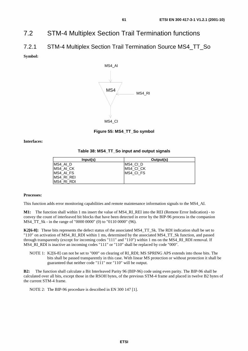
ETSI
ETSI EN 300 417-3-1 V1.2.1 (2001-10)61
7.2 STM-4 Multiplex Section Trail Termination functions
7.2.1 STM-4 Multiplex Section Trail Termination Source MS4_TT_So
Symbol:
MS4
MS4_AI
MS4_CI
MS4_RI
Figure 55: MS4_TT_So symbol
Interfaces:
Table 38: MS4_TT_So input and output signals
Input(s) Output(s) MS4_AI_D MS4_AI_CK MS4_AI_FS MS4_RI_REI MS4_RI_RDI
MS4_CI_D MS4_CI_CK MS4_CI_FS
Processes:
This function adds error monitoring capabilities and remote maintenance information signals to the MS4_AI.
M1: The function shall within 1 ms insert the value of MS4_RI_REI into the REI (Remote Error Indication) - to convey the count of interleaved bit blocks that have been detected in error by the BIP-96 process in the companion MS4_TT_Sk - in the range of "0000 0000" (0) to "0110 0000" (96).
K2[6-8]: These bits represents the defect status of the associated MS4_TT_Sk. The RDI indication shall be set to "110" on activation of MS4_RI_RDI within 1 ms, determined by the associated MS4_TT_Sk function, and passed through transparently (except for incoming codes "111" and "110") within 1 ms on the MS4_RI_RDI removal. If MS4_RI_RDI is inactive an incoming codes "111" or "110" shall be replaced by code "000".
NOTE 1: K2[6-8] can not be set to "000" on clearing of RI_RDI; MS SPRING APS extends into those bits. The bits shall be passed transparently in this case. With linear MS protection or without protection it shall be guaranteed that neither code "111" nor "110" will be output.
B2: The function shall calculate a Bit Interleaved Parity 96 (BIP-96) code using even parity. The BIP-96 shall be calculated over all bits, except those in the RSOH bytes, of the previous STM-4 frame and placed in twelve B2 bytes of the current STM-4 frame.
NOTE 2: The BIP-96 procedure is described in EN 300 147 [1].
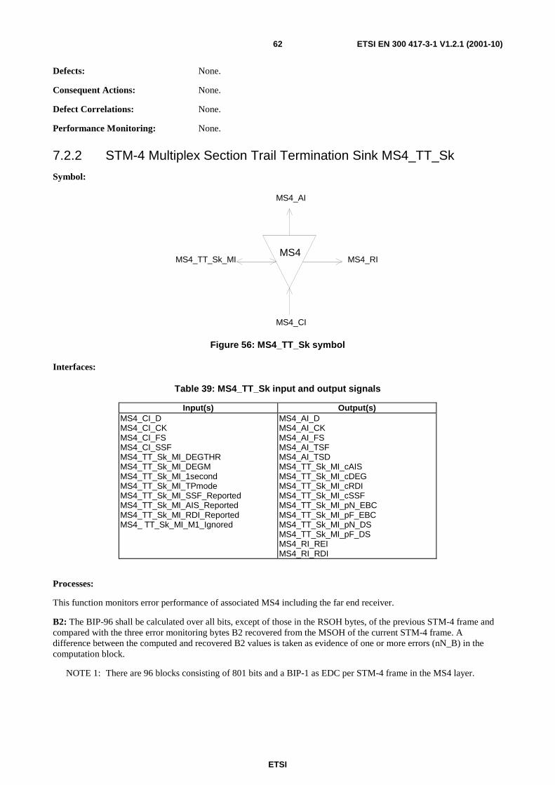
ETSI
ETSI EN 300 417-3-1 V1.2.1 (2001-10)62
Defects: None.
Consequent Actions: None.
Defect Correlations: None.
Performance Monitoring: None.
7.2.2 STM-4 Multiplex Section Trail Termination Sink MS4_TT_Sk
Symbol:
MS4
MS4_AI
MS4_CI
MS4_TT_Sk_MI MS4_RI
Figure 56: MS4_TT_Sk symbol
Interfaces:
Table 39: MS4_TT_Sk input and output signals
Input(s) Output(s) MS4_CI_D MS4_CI_CK MS4_CI_FS MS4_CI_SSF MS4_TT_Sk_MI_DEGTHR MS4_TT_Sk_MI_DEGM MS4_TT_Sk_MI_1second MS4_TT_Sk_MI_TPmode MS4_TT_Sk_MI_SSF_Reported MS4_TT_Sk_MI_AIS_Reported MS4_TT_Sk_MI_RDI_Reported MS4_ TT_Sk_MI_M1_Ignored
MS4_AI_D MS4_AI_CK MS4_AI_FS MS4_AI_TSF MS4_AI_TSD MS4_TT_Sk_MI_cAIS MS4_TT_Sk_MI_cDEG MS4_TT_Sk_MI_cRDI MS4_TT_Sk_MI_cSSF MS4_TT_Sk_MI_pN_EBC MS4_TT_Sk_MI_pF_EBC MS4_TT_Sk_MI_pN_DS MS4_TT_Sk_MI_pF_DS MS4_RI_REI MS4_RI_RDI
Processes:
This function monitors error performance of associated MS4 including the far end receiver.
B2: The BIP-96 shall be calculated over all bits, except of those in the RSOH bytes, of the previous STM-4 frame and compared with the three error monitoring bytes B2 recovered from the MSOH of the current STM-4 frame. A difference between the computed and recovered B2 values is taken as evidence of one or more errors (nN_B) in the computation block.
NOTE 1: There are 96 blocks consisting of 801 bits and a BIP-1 as EDC per STM-4 frame in the MS4 layer.
ETSI
ETSI EN 300 417-3-1 V1.2.1 (2001-10)63
M1: The REI information carried in these bits shall be extracted to enable single ended maintenance of a bi-directional trail (section). The REI (nF_B) is used to monitor the error performance of the other direction of transmission. The application process is described in EN 300 417-1-1 [3], clause 7.4.2 (REI). If M1_ignored is true, nF_B shall be forced to "0"; if M1_ignored is false, nF_B shall equal the value in REI.
NOTE 2: M1_ignored is a parameter provisioned by the operator to indicate the support of the M1 byte in the incoming STM-4 signal. For the case M1 is supported, M1_ignored should be set to false, otherwise M1_ignored should be set to true.
The function shall interpret the value in the byte (to allow interworking with old equipment generating a 7 bit code), as shown in table 40.
Table 40: STM-4 M1 interpretation
M1[2-8] code, bits 234 5678
code interpretation [#BIP violations], (nF_B)
000 0000 0 000 0001 1 000 0010 2 000 0011 3 000 0100 4 000 0101 5
M M 110 0000 96 110 0001 0 110 0010 0
M M 111 1111 0
NOTE: Bit 1 of byte M1 is ignored.
NOTE 3: In case of interworking with old equipment not supporting MS-REI, the information extracted from M1 is not relevant.
K2[6-8] - RDI: The RDI information carried in these bits shall be extracted to enable single ended maintenance of a bi-directional trail (section). The RDI provides information as to the status of the remote receiver. A "110" indicates a Remote Defect Indication state, while other patterns indicate the normal state. The application process is described in EN 300 417-1-1 [3], clauses 7.4.11 and 8.2.
K2[6-8] - AIS: The MS-AIS information carried in these bits shall be extracted.
Defects:
The function shall detect for dDEG and dRDI defects according the specification in EN 300 417-1-1 [3], clause 8.2.1.
dAIS: If at least x consecutive frames contain the "111" pattern in bits 6, 7 and 8 of the K2 byte a dAIS defect shall be detected. dAIS shall be cleared if in at least x consecutive frames any pattern other then the "111" is detected in bits 6, 7 and 8 of byte K2. The x shall be in range 3 to 5.
Consequent Actions:
aAIS ← dAIS.
aRDI ← dAIS.
aREI ← #EDCV.
aTSF ← dAIS.
aTSD ← dDEG.
On declaration of aAIS the function shall output an all-ONEs signal within 250 µs; on clearing of aAIS the function shall output normal data within 250 µs.
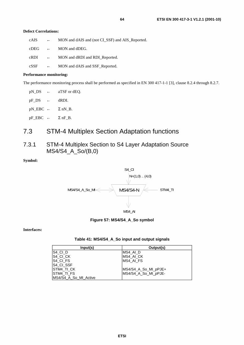
ETSI
ETSI EN 300 417-3-1 V1.2.1 (2001-10)64
Defect Correlations:
cAIS ← MON and dAIS and (not CI_SSF) and AIS_Reported.
cDEG ← MON and dDEG.
cRDI ← MON and dRDI and RDI_Reported.
cSSF ← MON and dAIS and SSF_Reported.
Performance monitoring:
The performance monitoring process shall be performed as specified in EN 300 417-1-1 [3], clause 8.2.4 through 8.2.7.
pN_DS ← aTSF or dEQ.
pF_DS ← dRDI.
pN_EBC ← Σ nN_B.
pF_EBC ← Σ nF_B.
7.3 STM-4 Multiplex Section Adaptation functions
7.3.1 STM-4 Multiplex Section to S4 Layer Adaptation Source MS4/S4_A_So/(B,0)
Symbol:
MS4/S4-N
S4_CI
MS4_AI
MS4/S4_A_So_MI STM4_TI
N=(1,0) .. (4,0)
Figure 57: MS4/S4_A_So symbol
Interfaces:
Table 41: MS4/S4_A_So input and output signals
Input(s) Output(s) S4_CI_D S4_CI_CK S4_CI_FS S4_CI_SSF STM4_TI_CK STM4_TI_FS MS4/S4_A_So_MI_Active
MS4_AI_D MS4_AI_CK MS4_AI_FS MS4/S4_A_So_MI_pPJE+ MS4/S4_A_So_MI_pPJE-
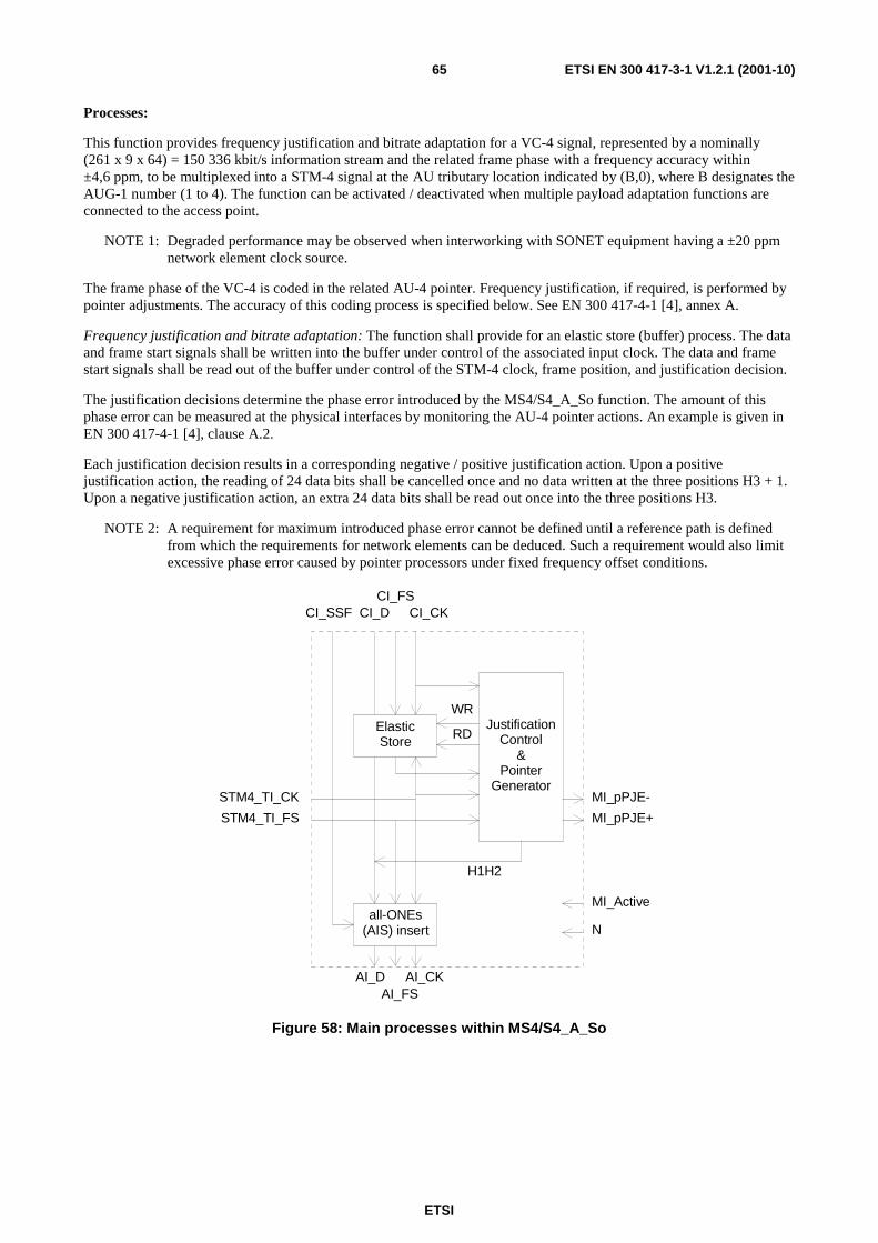
ETSI
ETSI EN 300 417-3-1 V1.2.1 (2001-10)65
Processes:
This function provides frequency justification and bitrate adaptation for a VC-4 signal, represented by a nominally (261 x 9 x 64) = 150 336 kbit/s information stream and the related frame phase with a frequency accuracy within ±4,6 ppm, to be multiplexed into a STM-4 signal at the AU tributary location indicated by (B,0), where B designates the AUG-1 number (1 to 4). The function can be activated / deactivated when multiple payload adaptation functions are connected to the access point.
NOTE 1: Degraded performance may be observed when interworking with SONET equipment having a ±20 ppm network element clock source.
The frame phase of the VC-4 is coded in the related AU-4 pointer. Frequency justification, if required, is performed by pointer adjustments. The accuracy of this coding process is specified below. See EN 300 417-4-1 [4], annex A.
Frequency justification and bitrate adaptation: The function shall provide for an elastic store (buffer) process. The data and frame start signals shall be written into the buffer under control of the associated input clock. The data and frame start signals shall be read out of the buffer under control of the STM-4 clock, frame position, and justification decision.
The justification decisions determine the phase error introduced by the MS4/S4_A_So function. The amount of this phase error can be measured at the physical interfaces by monitoring the AU-4 pointer actions. An example is given in EN 300 417-4-1 [4], clause A.2.
Each justification decision results in a corresponding negative / positive justification action. Upon a positive justification action, the reading of 24 data bits shall be cancelled once and no data written at the three positions H3 + 1. Upon a negative justification action, an extra 24 data bits shall be read out once into the three positions H3.
NOTE 2: A requirement for maximum introduced phase error cannot be defined until a reference path is defined from which the requirements for network elements can be deduced. Such a requirement would also limit excessive phase error caused by pointer processors under fixed frequency offset conditions.
ElasticStore
JustificationControl
&Pointer
Generator
STM4_TI_FS
STM4_TI_CK
WR
RD
all-ONEs(AIS) insert
CI_SSF CI_DCI_FS
CI_CK
AI_DAI_FS
AI_CK
H1H2
MI_pPJE-
MI_pPJE+
MI_Active
N
Figure 58: Main processes within MS4/S4_A_So
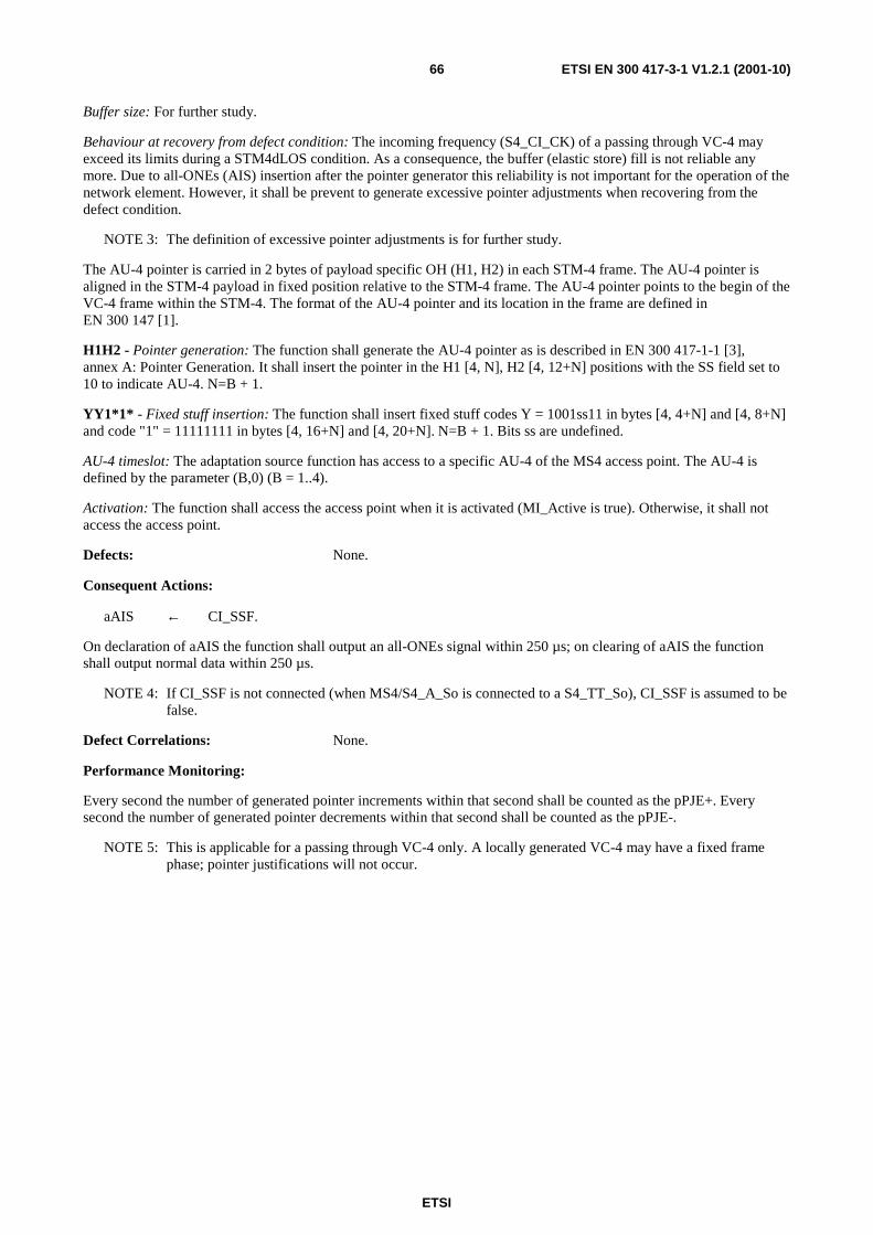
ETSI
ETSI EN 300 417-3-1 V1.2.1 (2001-10)66
Buffer size: For further study.
Behaviour at recovery from defect condition: The incoming frequency (S4_CI_CK) of a passing through VC-4 may exceed its limits during a STM4dLOS condition. As a consequence, the buffer (elastic store) fill is not reliable any more. Due to all-ONEs (AIS) insertion after the pointer generator this reliability is not important for the operation of the network element. However, it shall be prevent to generate excessive pointer adjustments when recovering from the defect condition.
NOTE 3: The definition of excessive pointer adjustments is for further study.
The AU-4 pointer is carried in 2 bytes of payload specific OH (H1, H2) in each STM-4 frame. The AU-4 pointer is aligned in the STM-4 payload in fixed position relative to the STM-4 frame. The AU-4 pointer points to the begin of the VC-4 frame within the STM-4. The format of the AU-4 pointer and its location in the frame are defined in EN 300 147 [1].
H1H2 - Pointer generation: The function shall generate the AU-4 pointer as is described in EN 300 417-1-1 [3], annex A: Pointer Generation. It shall insert the pointer in the H1 [4, N], H2 [4, 12+N] positions with the SS field set to 10 to indicate AU-4. N=B + 1.
YY1*1* - Fixed stuff insertion: The function shall insert fixed stuff codes Y = 1001ss11 in bytes [4, 4+N] and [4, 8+N] and code "1" = 11111111 in bytes [4, 16+N] and [4, 20+N]. N=B + 1. Bits ss are undefined.
AU-4 timeslot: The adaptation source function has access to a specific AU-4 of the MS4 access point. The AU-4 is defined by the parameter (B,0) (B = 1..4).
Activation: The function shall access the access point when it is activated (MI_Active is true). Otherwise, it shall not access the access point.
Defects: None.
Consequent Actions:
aAIS ← CI_SSF.
On declaration of aAIS the function shall output an all-ONEs signal within 250 µs; on clearing of aAIS the function shall output normal data within 250 µs.
NOTE 4: If CI_SSF is not connected (when MS4/S4_A_So is connected to a S4_TT_So), CI_SSF is assumed to be false.
Defect Correlations: None.
Performance Monitoring:
Every second the number of generated pointer increments within that second shall be counted as the pPJE+. Every second the number of generated pointer decrements within that second shall be counted as the pPJE-.
NOTE 5: This is applicable for a passing through VC-4 only. A locally generated VC-4 may have a fixed frame phase; pointer justifications will not occur.
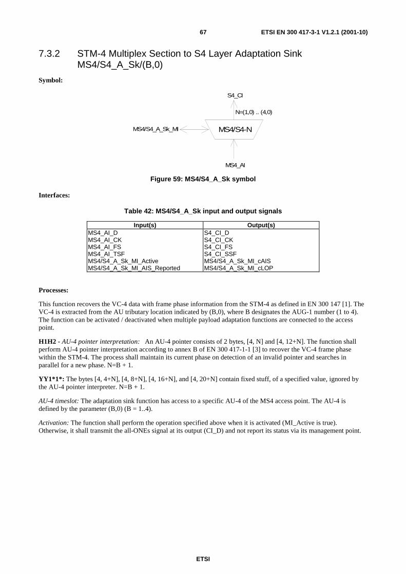
ETSI
ETSI EN 300 417-3-1 V1.2.1 (2001-10)67
7.3.2 STM-4 Multiplex Section to S4 Layer Adaptation Sink MS4/S4_A_Sk/(B,0)
Symbol:
MS4/S4-N
S4_CI
MS4_AI
MS4/S4_A_Sk_MI
N=(1,0) .. (4,0)
Figure 59: MS4/S4_A_Sk symbol
Interfaces:
Table 42: MS4/S4_A_Sk input and output signals
Input(s) Output(s) MS4_AI_D MS4_AI_CK MS4_AI_FS MS4_AI_TSF MS4/S4_A_Sk_MI_Active MS4/S4_A_Sk_MI_AIS_Reported
S4_CI_D S4_CI_CK S4_CI_FS S4_CI_SSF MS4/S4_A_Sk_MI_cAIS MS4/S4_A_Sk_MI_cLOP
Processes:
This function recovers the VC-4 data with frame phase information from the STM-4 as defined in EN 300 147 [1]. The VC-4 is extracted from the AU tributary location indicated by (B,0), where B designates the AUG-1 number (1 to 4). The function can be activated / deactivated when multiple payload adaptation functions are connected to the access point.
H1H2 - AU-4 pointer interpretation: An AU-4 pointer consists of 2 bytes, [4, N] and [4, 12+N]. The function shall perform AU-4 pointer interpretation according to annex B of EN 300 417-1-1 [3] to recover the VC-4 frame phase within the STM-4. The process shall maintain its current phase on detection of an invalid pointer and searches in parallel for a new phase. N=B + 1.
YY1*1*: The bytes [4, 4+N], [4, 8+N], [4, 16+N], and [4, 20+N] contain fixed stuff, of a specified value, ignored by the AU-4 pointer interpreter. N=B + 1.
AU-4 timeslot: The adaptation sink function has access to a specific AU-4 of the MS4 access point. The AU-4 is defined by the parameter (B,0) (B = 1..4).
Activation: The function shall perform the operation specified above when it is activated (MI_Active is true). Otherwise, it shall transmit the all-ONEs signal at its output (CI_D) and not report its status via its management point.
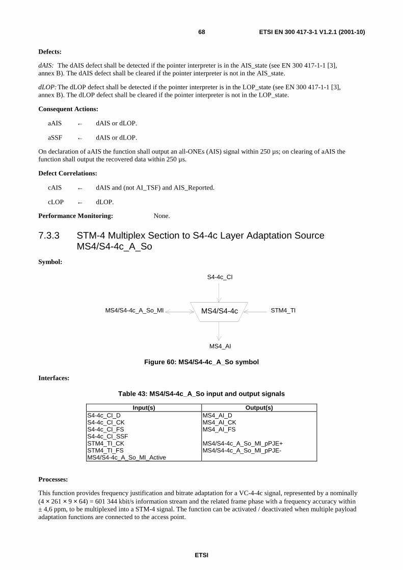
ETSI
ETSI EN 300 417-3-1 V1.2.1 (2001-10)68
Defects:
dAIS: The dAIS defect shall be detected if the pointer interpreter is in the AIS_state (see EN 300 417-1-1 [3], annex B). The dAIS defect shall be cleared if the pointer interpreter is not in the AIS_state.
dLOP: The dLOP defect shall be detected if the pointer interpreter is in the LOP_state (see EN 300 417-1-1 [3], annex B). The dLOP defect shall be cleared if the pointer interpreter is not in the LOP_state.
Consequent Actions:
aAIS ← dAIS or dLOP.
aSSF ← dAIS or dLOP.
On declaration of aAIS the function shall output an all-ONEs (AIS) signal within 250 µs; on clearing of aAIS the function shall output the recovered data within 250 µs.
Defect Correlations:
cAIS ← dAIS and (not AI_TSF) and AIS_Reported.
cLOP ← dLOP.
Performance Monitoring: None.
7.3.3 STM-4 Multiplex Section to S4-4c Layer Adaptation Source MS4/S4-4c_A_So
Symbol:
MS4/S4-4c
S4-4c_CI
MS4_AI
MS4/S4-4c_A_So_MI STM4_TI
Figure 60: MS4/S4-4c_A_So symbol
Interfaces:
Table 43: MS4/S4-4c_A_So input and output signals
Input(s) Output(s) S4-4c_CI_D S4-4c_CI_CK S4-4c_CI_FS S4-4c_CI_SSF STM4_TI_CK STM4_TI_FS MS4/S4-4c_A_So_MI_Active
MS4_AI_D MS4_AI_CK MS4_AI_FS MS4/S4-4c_A_So_MI_pPJE+ MS4/S4-4c_A_So_MI_pPJE-
Processes:
This function provides frequency justification and bitrate adaptation for a VC-4-4c signal, represented by a nominally (4 × 261 × 9 × 64) = 601 344 kbit/s information stream and the related frame phase with a frequency accuracy within ± 4,6 ppm, to be multiplexed into a STM-4 signal. The function can be activated / deactivated when multiple payload adaptation functions are connected to the access point.
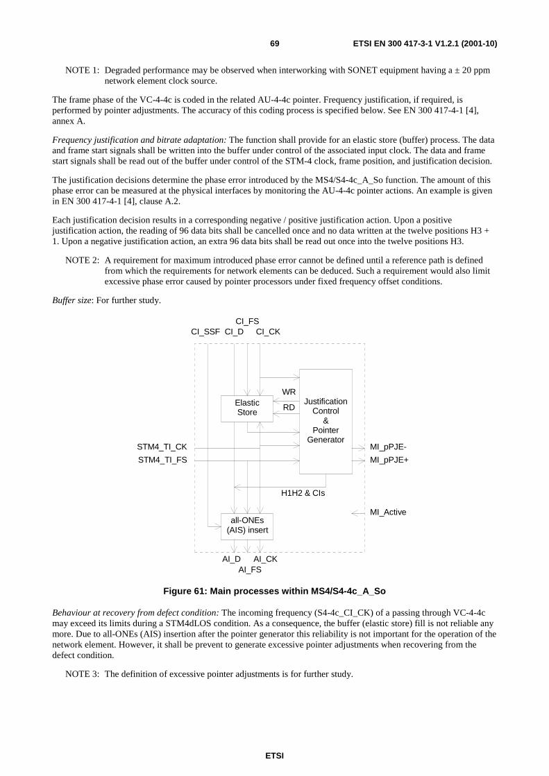
ETSI
ETSI EN 300 417-3-1 V1.2.1 (2001-10)69
NOTE 1: Degraded performance may be observed when interworking with SONET equipment having a ± 20 ppm network element clock source.
The frame phase of the VC-4-4c is coded in the related AU-4-4c pointer. Frequency justification, if required, is performed by pointer adjustments. The accuracy of this coding process is specified below. See EN 300 417-4-1 [4], annex A.
Frequency justification and bitrate adaptation: The function shall provide for an elastic store (buffer) process. The data and frame start signals shall be written into the buffer under control of the associated input clock. The data and frame start signals shall be read out of the buffer under control of the STM-4 clock, frame position, and justification decision.
The justification decisions determine the phase error introduced by the MS4/S4-4c_A_So function. The amount of this phase error can be measured at the physical interfaces by monitoring the AU-4-4c pointer actions. An example is given in EN 300 417-4-1 [4], clause A.2.
Each justification decision results in a corresponding negative / positive justification action. Upon a positive justification action, the reading of 96 data bits shall be cancelled once and no data written at the twelve positions H3 + 1. Upon a negative justification action, an extra 96 data bits shall be read out once into the twelve positions H3.
NOTE 2: A requirement for maximum introduced phase error cannot be defined until a reference path is defined from which the requirements for network elements can be deduced. Such a requirement would also limit excessive phase error caused by pointer processors under fixed frequency offset conditions.
Buffer size: For further study.
ElasticStore
JustificationControl
&Pointer
Generator
STM4_TI_FS
STM4_TI_CK
WR
RD
all-ONEs(AIS) insert
CI_SSF CI_DCI_FS
CI_CK
AI_DAI_FS
AI_CK
H1H2 & CIs
MI_pPJE-
MI_pPJE+
MI_Active
Figure 61: Main processes within MS4/S4-4c_A_So
Behaviour at recovery from defect condition: The incoming frequency (S4-4c_CI_CK) of a passing through VC-4-4c may exceed its limits during a STM4dLOS condition. As a consequence, the buffer (elastic store) fill is not reliable any more. Due to all-ONEs (AIS) insertion after the pointer generator this reliability is not important for the operation of the network element. However, it shall be prevent to generate excessive pointer adjustments when recovering from the defect condition.
NOTE 3: The definition of excessive pointer adjustments is for further study.
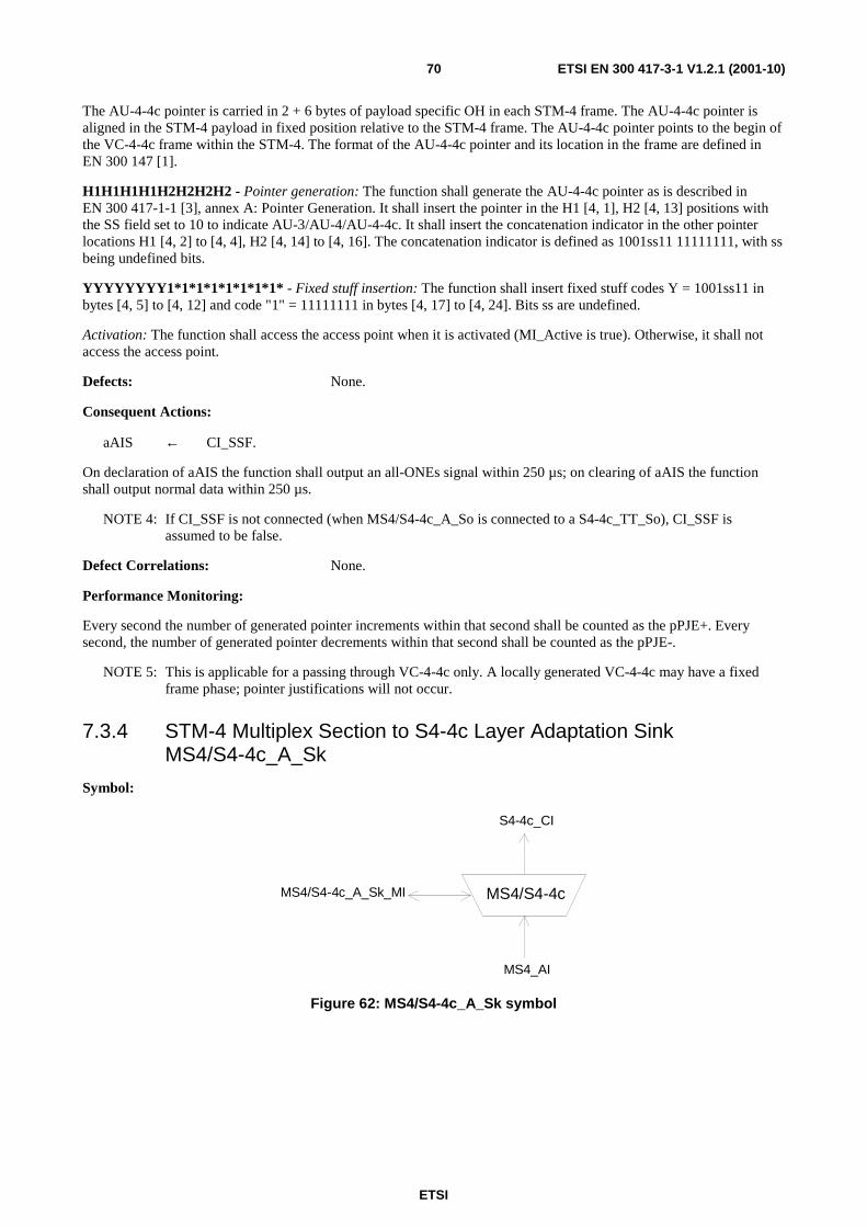
ETSI
ETSI EN 300 417-3-1 V1.2.1 (2001-10)70
The AU-4-4c pointer is carried in 2 + 6 bytes of payload specific OH in each STM-4 frame. The AU-4-4c pointer is aligned in the STM-4 payload in fixed position relative to the STM-4 frame. The AU-4-4c pointer points to the begin of the VC-4-4c frame within the STM-4. The format of the AU-4-4c pointer and its location in the frame are defined in EN 300 147 [1].
H1H1H1H1H2H2H2H2 - Pointer generation: The function shall generate the AU-4-4c pointer as is described in EN 300 417-1-1 [3], annex A: Pointer Generation. It shall insert the pointer in the H1 [4, 1], H2 [4, 13] positions with the SS field set to 10 to indicate AU-3/AU-4/AU-4-4c. It shall insert the concatenation indicator in the other pointer locations H1 [4, 2] to [4, 4], H2 [4, 14] to [4, 16]. The concatenation indicator is defined as 1001ss11 11111111, with ss being undefined bits.
YYYYYYYY1*1*1*1*1*1*1*1* - Fixed stuff insertion: The function shall insert fixed stuff codes Y = 1001ss11 in bytes [4, 5] to [4, 12] and code "1" = 11111111 in bytes [4, 17] to [4, 24]. Bits ss are undefined.
Activation: The function shall access the access point when it is activated (MI_Active is true). Otherwise, it shall not access the access point.
Defects: None.
Consequent Actions:
aAIS ← CI_SSF.
On declaration of aAIS the function shall output an all-ONEs signal within 250 µs; on clearing of aAIS the function shall output normal data within 250 µs.
NOTE 4: If CI_SSF is not connected (when MS4/S4-4c_A_So is connected to a S4-4c_TT_So), CI_SSF is assumed to be false.
Defect Correlations: None.
Performance Monitoring:
Every second the number of generated pointer increments within that second shall be counted as the pPJE+. Every second, the number of generated pointer decrements within that second shall be counted as the pPJE-.
NOTE 5: This is applicable for a passing through VC-4-4c only. A locally generated VC-4-4c may have a fixed frame phase; pointer justifications will not occur.
7.3.4 STM-4 Multiplex Section to S4-4c Layer Adaptation Sink MS4/S4-4c_A_Sk
Symbol:
MS4/S4-4c
S4-4c_CI
MS4_AI
MS4/S4-4c_A_Sk_MI
Figure 62: MS4/S4-4c_A_Sk symbol
ETSI
ETSI EN 300 417-3-1 V1.2.1 (2001-10)71
Interfaces:
Table 44: MS4/S4-4c_A_Sk input and output signals
Input(s) Output(s) MS4_AI_D MS4_AI_CK MS4_AI_FS MS4_AI_TSF MS4/S4-4c_A_Sk_MI_Active MS4/S4-4c_A_Sk_MI_AIS_Reported
S4-4c_CI_D S4-4c_CI_CK S4-4c_CI_FS S4-4c_CI_SSF MS4/S4-4c_A_Sk_MI_cAIS MS4/S4-4c_A_Sk_MI_cLOP
Processes:
This function recovers the VC-4-4c data with frame phase information from the STM-4 as defined in EN 300 147 [1]. The function can be activated / deactivated when multiple payload adaptation functions are connected to the access point.
H1H2 - AU-4-4c pointer interpretation: An AU-4-4c pointer consists of 4 x 2 bytes, [4, 1]/[4, 13], [4, 2]/[4, 14], [4, 3]/[4, 15], and [4, 4]/[4, 16]. The last three pairs of pointer bytes contain the concatenation indication. The function shall perform AU-4-4c pointer interpretation according to annex B of EN 300 417-1-1 [3] to recover the VC-4-4c frame phase within the STM-4. The process shall maintain its current phase on detection of an invalid pointer and searches in parallel for a new phase.
YY1*1*: The bytes [4, 5] to [4, 12] and [4, 17] to [4, 24] contain fixed stuff, of a specified value, ignored by the AU-4-4c pointer interpreter.
Activation: The function shall perform the operation specified above when it is activated (MI_Active is true). Otherwise, it shall transmit the all-ONEs signal at its output (CI_D) and not report its status via its management point.
Defects:
dAIS: The dAIS defect shall be detected if the pointer interpreter is in the AISX_state (see EN 300 417-1-1 [3], annex B). The dAIS defect shall be cleared if the pointer interpreter is not in the AISX_state.
dLOP: The dLOP defect shall be detected if the pointer interpreter is in the LOPX_state (see EN 300 417-1-1 [3], annex B). The dLOP defect shall be cleared if the pointer interpreter is not in the LOPX_state.
Consequent Actions:
aAIS ← dAIS or dLOP.
aSSF ← dAIS or dLOP.
On declaration of aAIS the function shall output an all-ONEs (AIS) signal within 250 µs; on clearing of aAIS the function shall output the recovered data within 250 µs.
Defect Correlations:
cAIS ← dAIS and (not aTSF) and AIS_Reported.
cLOP ← dLOP.
Performance Monitoring: None.
ETSI
ETSI EN 300 417-3-1 V1.2.1 (2001-10)72
7.3.5 STM-4 Multiplex Section to DCC Adaptation Source MS4/DCC_A_So
Symbol:
MS4/DCC
DCC_CI_D
MS4_AI
STM4_TI
DCC_CI_CK
Figure 63: MS4/DCC_A_So symbol
Interfaces:
Table 45: MS4/DCC_A_So input and output signals
Input(s) Output(s) DCC_CI_D STM4_TI_CK STM4_TI_FS
MS4_AI_D DCC_CI_CK
Processes:
The function multiplexes the DCC CI data (576 kbit/s) into the byte locations D4 to D12 as defined in EN 300 147 [1] and depicted in figure 52.
NOTE: DCC transmission can be "disabled" when the matrix connection in the connected DCC_C function is removed.
Defects: None.
Consequent Actions: None.
Defect Correlations: None.
Performance Monitoring: None.
7.3.6 STM-4 Multiplex Section to DCC Adaptation Sink MS4/DCC_A_Sk
Symbol:
MS4/DCC
DCC_CI
MS4_AI
Figure 64: MS4/DCC_A_Sk symbol
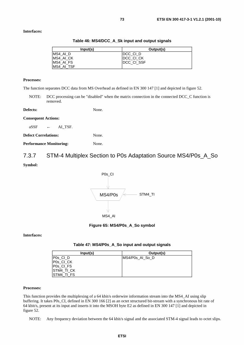
ETSI
ETSI EN 300 417-3-1 V1.2.1 (2001-10)73
Interfaces:
Table 46: MS4/DCC_A_Sk input and output signals
Input(s) Output(s) MS4_AI_D MS4_AI_CK MS4_AI_FS MS4_AI_TSF
DCC_CI_D DCC_CI_CK DCC_CI_SSF
Processes:
The function separates DCC data from MS Overhead as defined in EN 300 147 [1] and depicted in figure 52.
NOTE: DCC processing can be "disabled" when the matrix connection in the connected DCC_C function is removed.
Defects: None.
Consequent Actions:
aSSF ← AI_TSF.
Defect Correlations: None.
Performance Monitoring: None.
7.3.7 STM-4 Multiplex Section to P0s Adaptation Source MS4/P0s_A_So
Symbol:
MS4/P0s
P0s_CI
MS4_AI
STM4_TI
Figure 65: MS4/P0s_A_So symbol
Interfaces:
Table 47: MS4/P0s_A_So input and output signals
Input(s) Output(s) P0s_CI_D P0s_CI_CK P0s_CI_FS STM4_TI_CK STM4_TI_FS
MS4/P0s_AI_So_D
Processes:
This function provides the multiplexing of a 64 kbit/s orderwire information stream into the MS4_AI using slip buffering. It takes P0s_CI, defined in EN 300 166 [2] as an octet structured bit-stream with a synchronous bit rate of 64 kbit/s, present at its input and inserts it into the MSOH byte E2 as defined in EN 300 147 [1] and depicted in figure 52.
NOTE: Any frequency deviation between the 64 kbit/s signal and the associated STM-4 signal leads to octet slips.
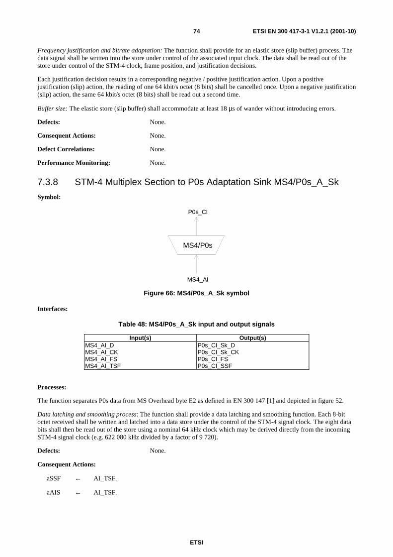
ETSI
ETSI EN 300 417-3-1 V1.2.1 (2001-10)74
Frequency justification and bitrate adaptation: The function shall provide for an elastic store (slip buffer) process. The data signal shall be written into the store under control of the associated input clock. The data shall be read out of the store under control of the STM-4 clock, frame position, and justification decisions.
Each justification decision results in a corresponding negative / positive justification action. Upon a positive justification (slip) action, the reading of one 64 kbit/s octet (8 bits) shall be cancelled once. Upon a negative justification (slip) action, the same 64 kbit/s octet (8 bits) shall be read out a second time.
Buffer size: The elastic store (slip buffer) shall accommodate at least 18 µs of wander without introducing errors.
Defects: None.
Consequent Actions: None.
Defect Correlations: None.
Performance Monitoring: None.
7.3.8 STM-4 Multiplex Section to P0s Adaptation Sink MS4/P0s_A_Sk
Symbol:
MS4/P0s
P0s_CI
MS4_AI
Figure 66: MS4/P0s_A_Sk symbol
Interfaces:
Table 48: MS4/P0s_A_Sk input and output signals
Input(s) Output(s) MS4_AI_D MS4_AI_CK MS4_AI_FS MS4_AI_TSF
P0s_CI_Sk_D P0s_CI_Sk_CK P0s_CI_FS P0s_CI_SSF
Processes:
The function separates P0s data from MS Overhead byte E2 as defined in EN 300 147 [1] and depicted in figure 52.
Data latching and smoothing process: The function shall provide a data latching and smoothing function. Each 8-bit octet received shall be written and latched into a data store under the control of the STM-4 signal clock. The eight data bits shall then be read out of the store using a nominal 64 kHz clock which may be derived directly from the incoming STM-4 signal clock (e.g. 622 080 kHz divided by a factor of 9 720).
Defects: None.
Consequent Actions:
aSSF ← AI_TSF.
aAIS ← AI_TSF.
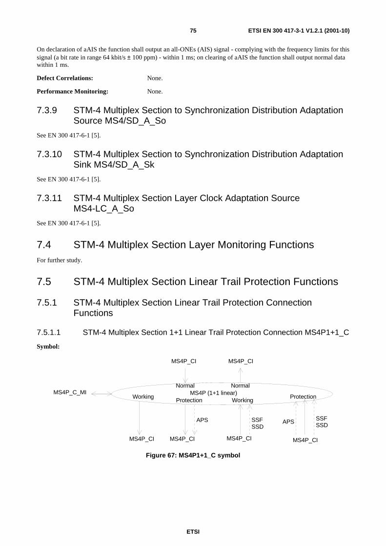
ETSI
ETSI EN 300 417-3-1 V1.2.1 (2001-10)75
On declaration of aAIS the function shall output an all-ONEs (AIS) signal - complying with the frequency limits for this signal (a bit rate in range 64 kbit/s ± 100 ppm) - within 1 ms; on clearing of aAIS the function shall output normal data within 1 ms.
Defect Correlations: None.
Performance Monitoring: None.
7.3.9 STM-4 Multiplex Section to Synchronization Distribution Adaptation Source MS4/SD_A_So
See EN 300 417-6-1 [5].
7.3.10 STM-4 Multiplex Section to Synchronization Distribution Adaptation Sink MS4/SD_A_Sk
See EN 300 417-6-1 [5].
7.3.11 STM-4 Multiplex Section Layer Clock Adaptation Source MS4-LC_A_So
See EN 300 417-6-1 [5].
7.4 STM-4 Multiplex Section Layer Monitoring Functions For further study.
7.5 STM-4 Multiplex Section Linear Trail Protection Functions
7.5.1 STM-4 Multiplex Section Linear Trail Protection Connection Functions
7.5.1.1 STM-4 Multiplex Section 1+1 Linear Trail Protection Connection MS4P1+1_C
Symbol:
MS4P_CI MS4P_CI
MS4P (1+1 linear)
APS SSFSSD
WorkingProtection Working
APS SSFSSD
Protection
MS4P_CI MS4P_CI
MS4P_CI MS4P_CI
Normal NormalMS4P_C_MI
Figure 67: MS4P1+1_C symbol

ETSI
ETSI EN 300 417-3-1 V1.2.1 (2001-10)76
Interfaces:
Table 49: MS4P1+1_C input and output signals
Input(s) Output(s) For connection points W and P: MS4P_CI_D MS4P_CI_CK MS4P_CI_FS MS4P_CI_SSF MS4P_CI_SSD For connection points N: MS4P_CI_D MS4P_CI_CK MS4P_CI_FS Per function: MS4P_CI_APS MS4P_C_MI_SWtype MS4P_C_MI_OPERtype MS4P_C_MI_WTRTime MS4P_C_MI_EXTCMD
For connection points W and P: MS4P_CI_D MS4P_CI_CK MS4P_CI_FS MS4P_CI_SSF For connection points N: MS4P_CI_D MS4P_CI_CK MS4P_CI_FS MS4P_CI_SSF Per function: MS4P_CI_APS MS4P_C_MI_cFOP
NOTE: Protection status reporting signals are for further study.
Processes:
The function performs the STM-4 linear multiplex section protection process for 1 + 1 protection architectures; see EN 300 417-1-1 [3], clause 9.2. It performs the bridge and selector functionality as presented in figure 48 of EN 300 417-1-1 [3]. In the sink direction, the signal output at the normal #1 reference point can be the signal received via either the associated working #1 section or the protection section; this is determined by the SF, SD conditions (relayed via CI_SSF, CI_SSD signals), the external commands and the information relayed via the APS signal. In the source direction, the working outputs are connected to the associated normal inputs. The protection output is connected to the normal #1 input.
Provided no protection switching action is activated / required, the following changes to (the configuration of) a connection shall be possible without disturbing the CI passing the connection:
- change between switching types;
- change between operation types;
- change of WTR time.
MS Protection Operation: The MS trail protection process shall operate as specified in annex A, according the following characteristics:
Table 50 "Parameters for MS41P1+1_C protection process"
Architecture: 1 + 1 Switching type: uni-directional or bi-directional Operation type: revertive or non-revertive APS channel: 13 bits, K1[1-8] and K2[1-5] Wait-To-Restore time: in the order of 0-12 minutes Switching time: ≤ 50 ms Hold-off time: not applicable Signal switch conditions: SF, SD External commands: (revertive operation) LO, FSw-#1, MSw-#1, CLR, EXER-#1
(non-revertive operation) LO or FSw, FSw-#i, MSw, MSw-#i, CLR, EXER-#1
SFpriority, SDpriority: high
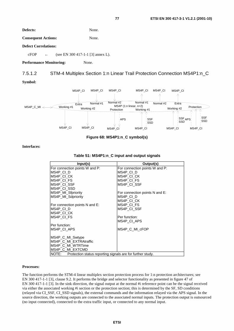
ETSI
ETSI EN 300 417-3-1 V1.2.1 (2001-10)77
Defects: None.
Consequent Actions: None.
Defect Correlations:
cFOP ← (see EN 300 417-1-1 [3] annex L).
Performance Monitoring: None.
7.5.1.2 STM-4 Multiplex Section 1:n Linear Trail Protection Connection MS4P1:n_C
Symbol:
MS4P_CI MS4P_CI
MS4P (1:n linear, n=2)
APS SSFSSD
Working #1Protection Working #1
MS4P_CI
Working #2
SSFSSD
Working #2
APSSSFSSD
Protection
MS4P_CI MS4P_CI MS4P_CI
MS4P_CI MS4P_CI MS4P_CI MS4P_CI
MS4P_C_MINormal #1 Normal #2Normal #1Normal #2
MS4P_CI
Extra
MS4P_CI
Extra
Figure 68: MS4P1:n_C symbol(s)
Interfaces:
Table 51: MS4P1:n_C input and output signals
Input(s) Output(s) For connection points W and P: MS4P_CI_D MS4P_CI_CK MS4P_CI_FS MS4P_CI_SSF MS4P_CI_SSD MS4P_MI_Sfpriority MS4P_MI_Sdpriority For connection points N and E: MS4P_CI_D MS4P_CI_CK MS4P_CI_FS Per function: MS4P_CI_APS MS4P_C_MI_Swtype MS4P_C_MI_EXTRAtraffic MS4P_C_MI_WTRTime MS4P_C_MI_EXTCMD
For connection points W and P: MS4P_CI_D MS4P_CI_CK MS4P_CI_FS MS4P_CI_SSF For connection points N and E: MS4P_CI_D MS4P_CI_CK MS4P_CI_FS MS4P_CI_SSF Per function: MS4P_CI_APS MS4P_C_MI_cFOP
NOTE: Protection status reporting signals are for further study.
Processes:
The function performs the STM-4 linear multiplex section protection process for 1:n protection architectures; see EN 300 417-1-1 [3], clause 9.2. It performs the bridge and selector functionality as presented in figure 47 of EN 300 417-1-1 [3]. In the sink direction, the signal output at the normal #i reference point can be the signal received via either the associated working #i section or the protection section; this is determined by the SF, SD conditions (relayed via CI_SSF, CI_SSD signals), the external commands and the information relayed via the APS signal. In the source direction, the working outputs are connected to the associated normal inputs. The protection output is outsourced (no input connected), connected to the extra traffic input, or connected to any normal input.
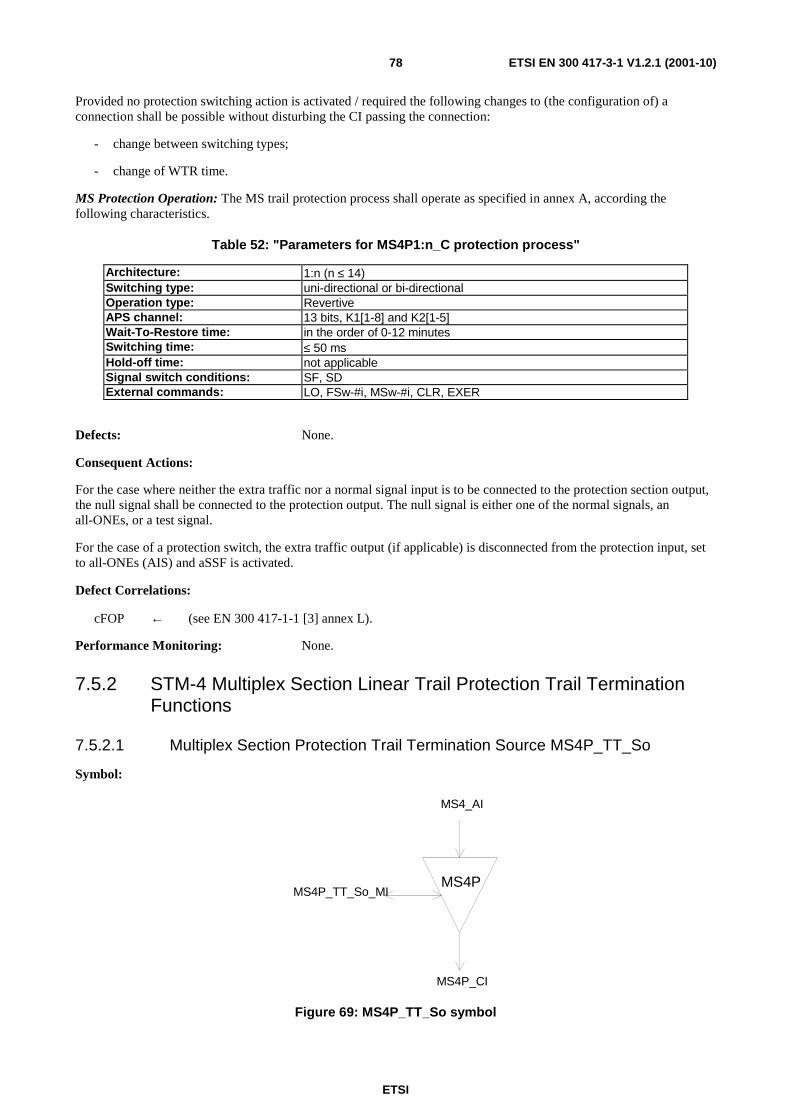
ETSI
ETSI EN 300 417-3-1 V1.2.1 (2001-10)78
Provided no protection switching action is activated / required the following changes to (the configuration of) a connection shall be possible without disturbing the CI passing the connection:
- change between switching types;
- change of WTR time.
MS Protection Operation: The MS trail protection process shall operate as specified in annex A, according the following characteristics.
Table 52: "Parameters for MS4P1:n_C protection process"
Architecture: 1:n (n ≤ 14) Switching type: uni-directional or bi-directional Operation type: Revertive APS channel: 13 bits, K1[1-8] and K2[1-5] Wait-To-Restore time: in the order of 0-12 minutes Switching time: ≤ 50 ms Hold-off time: not applicable Signal switch conditions: SF, SD External commands: LO, FSw-#i, MSw-#i, CLR, EXER
Defects: None.
Consequent Actions:
For the case where neither the extra traffic nor a normal signal input is to be connected to the protection section output, the null signal shall be connected to the protection output. The null signal is either one of the normal signals, an all-ONEs, or a test signal.
For the case of a protection switch, the extra traffic output (if applicable) is disconnected from the protection input, set to all-ONEs (AIS) and aSSF is activated.
Defect Correlations:
cFOP ← (see EN 300 417-1-1 [3] annex L).
Performance Monitoring: None.
7.5.2 STM-4 Multiplex Section Linear Trail Protection Trail Termination Functions
7.5.2.1 Multiplex Section Protection Trail Termination Source MS4P_TT_So
Symbol:
MS4P
MS4_AI
MS4P_CI
MS4P_TT_So_MI
Figure 69: MS4P_TT_So symbol
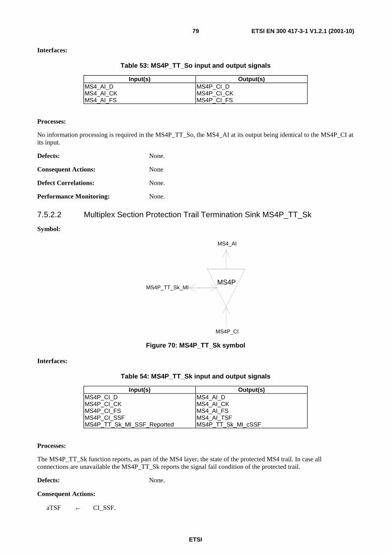
ETSI
ETSI EN 300 417-3-1 V1.2.1 (2001-10)79
Interfaces:
Table 53: MS4P_TT_So input and output signals
Input(s) Output(s) MS4_AI_D MS4_AI_CK MS4_AI_FS
MS4P_CI_D MS4P_CI_CK MS4P_CI_FS
Processes:
No information processing is required in the MS4P_TT_So, the MS4_AI at its output being identical to the MS4P_CI at its input.
Defects: None.
Consequent Actions: None
Defect Correlations: None.
Performance Monitoring: None.
7.5.2.2 Multiplex Section Protection Trail Termination Sink MS4P_TT_Sk
Symbol:
MS4P
MS4_AI
MS4P_CI
MS4P_TT_Sk_MI
Figure 70: MS4P_TT_Sk symbol
Interfaces:
Table 54: MS4P_TT_Sk input and output signals
Input(s) Output(s) MS4P_CI_D MS4P_CI_CK MS4P_CI_FS MS4P_CI_SSF MS4P_TT_Sk_MI_SSF_Reported
MS4_AI_D MS4_AI_CK MS4_AI_FS MS4_AI_TSF MS4P_TT_Sk_MI_cSSF
Processes:
The MS4P_TT_Sk function reports, as part of the MS4 layer, the state of the protected MS4 trail. In case all connections are unavailable the MS4P_TT_Sk reports the signal fail condition of the protected trail.
Defects: None.
Consequent Actions:
aTSF ← CI_SSF.
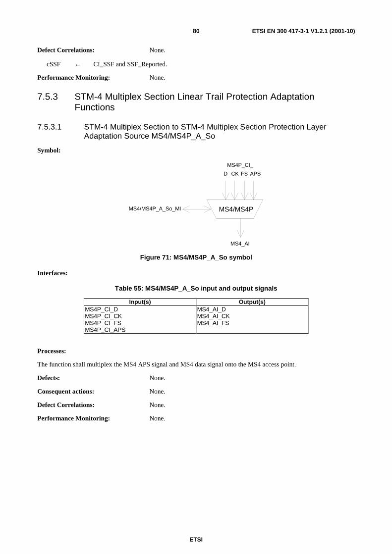
ETSI
ETSI EN 300 417-3-1 V1.2.1 (2001-10)80
Defect Correlations: None.
cSSF ← CI_SSF and SSF_Reported.
Performance Monitoring: None.
7.5.3 STM-4 Multiplex Section Linear Trail Protection Adaptation Functions
7.5.3.1 STM-4 Multiplex Section to STM-4 Multiplex Section Protection Layer Adaptation Source MS4/MS4P_A_So
Symbol:
MS4/MS4P
MS4P_CI_
MS4_AI
MS4/MS4P_A_So_MI
D CK FS APS
Figure 71: MS4/MS4P_A_So symbol
Interfaces:
Table 55: MS4/MS4P_A_So input and output signals
Input(s) Output(s) MS4P_CI_D MS4P_CI_CK MS4P_CI_FS MS4P_CI_APS
MS4_AI_D MS4_AI_CK MS4_AI_FS
Processes:
The function shall multiplex the MS4 APS signal and MS4 data signal onto the MS4 access point.
Defects: None.
Consequent actions: None.
Defect Correlations: None.
Performance Monitoring: None.
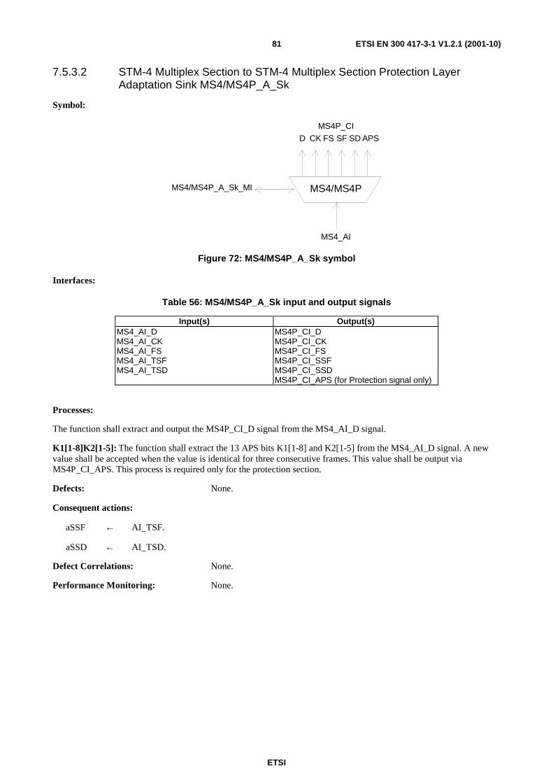
ETSI
ETSI EN 300 417-3-1 V1.2.1 (2001-10)81
7.5.3.2 STM-4 Multiplex Section to STM-4 Multiplex Section Protection Layer Adaptation Sink MS4/MS4P_A_Sk
Symbol:
MS4/MS4P
MS4P_CI
MS4_AI
MS4/MS4P_A_Sk_MI
D CK FS SF SD APS
Figure 72: MS4/MS4P_A_Sk symbol
Interfaces:
Table 56: MS4/MS4P_A_Sk input and output signals
Input(s) Output(s) MS4_AI_D MS4_AI_CK MS4_AI_FS MS4_AI_TSF MS4_AI_TSD
MS4P_CI_D MS4P_CI_CK MS4P_CI_FS MS4P_CI_SSF MS4P_CI_SSD MS4P_CI_APS (for Protection signal only)
Processes:
The function shall extract and output the MS4P_CI_D signal from the MS4_AI_D signal.
K1[1-8]K2[1-5]: The function shall extract the 13 APS bits K1[1-8] and K2[1-5] from the MS4_AI_D signal. A new value shall be accepted when the value is identical for three consecutive frames. This value shall be output via MS4P_CI_APS. This process is required only for the protection section.
Defects: None.
Consequent actions:
aSSF ← AI_TSF.
aSSD ← AI_TSD.
Defect Correlations: None.
Performance Monitoring: None.
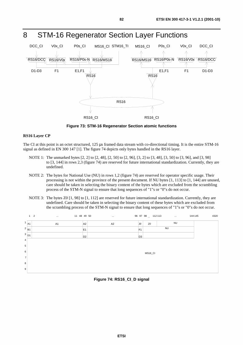
ETSI
ETSI EN 300 417-3-1 V1.2.1 (2001-10)82
8 STM-16 Regenerator Section Layer Functions
RS16
RS16/MS16
RS16
RS16/MS16
MS16_CI MS16_CI
RS16_CI RS16_CI
RS16/V0x RS16/V0xRS16/P0s-N
P0s_CISTM16_TI
RS16/P0s-N
P0s_CI
E1,F1 E1,F1
V0x_CIV0x_CI
RS16/DCC
DCC_CI
F1 D1-D3
RS16/DCC
DCC_CI
D1-D3 F1
RS16
Figure 73: STM-16 Regenerator Section atomic functions
RS16 Layer CP
The CI at this point is an octet structured, 125 µs framed data stream with co-directional timing. It is the entire STM-16 signal as defined in EN 300 147 [1]. The figure 74 depicts only bytes handled in the RS16 layer.
NOTE 1: The unmarked bytes [2, 2] to [2, 48], [2, 50] to [2, 96], [3, 2] to [3, 48], [3, 50] to [3, 96], and [3, 98] to [3, 144] in rows 2,3 (figure 74) are reserved for future international standardization. Currently, they are undefined.
NOTE 2: The bytes for National Use (NU) in rows 1,2 (figure 74) are reserved for operator specific usage. Their processing is not within the province of the present document. If NU bytes [1, 113] to [1, 144] are unused, care should be taken in selecting the binary content of the bytes which are excluded from the scrambling process of the STM-N signal to ensure that long sequences of "1"s or "0"s do not occur.
NOTE 3: The bytes Z0 [1, 98] to [1, 112] are reserved for future international standardization. Currently, they are undefined. Care should be taken in selecting the binary content of these bytes which are excluded from the scrambling process of the STM-N signal to ensure that long sequences of "1"s or "0"s do not occur.
A1
B1
D1
A1 A2
E1
D2
A2 J0 Z0
F1
D3
1
2
3
4
5
6
7
8
9
NU
1 2 ... 11 48 49 50 ... 96 97 98 112 113 ... 144 145 4320
MS16_CI
NU
...
Figure 74: RS16_CI_D signal
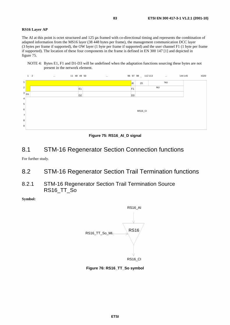
ETSI
ETSI EN 300 417-3-1 V1.2.1 (2001-10)83
RS16 Layer AP
The AI at this point is octet structured and 125 µs framed with co-directional timing and represents the combination of adapted information from the MS16 layer (38 448 bytes per frame), the management communication DCC layer (3 bytes per frame if supported), the OW layer (1 byte per frame if supported) and the user channel F1 (1 byte per frame if supported). The location of these four components in the frame is defined in EN 300 147 [1] and depicted in figure 75.
NOTE 4: Bytes E1, F1 and D1-D3 will be undefined when the adaptation functions sourcing these bytes are not present in the network element.
D1
E1
D2
J0 Z0
F1
D3
1
2
3
4
5
6
7
8
9
NU
1 2 ... 11 48 49 50 ... 96 97 98 112 113 ... 144 145 4320
MS16_CI
NU
...
Figure 75: RS16_AI_D signal
8.1 STM-16 Regenerator Section Connection functions For further study.
8.2 STM-16 Regenerator Section Trail Termination functions
8.2.1 STM-16 Regenerator Section Trail Termination Source RS16_TT_So
Symbol:
RS16
RS16_AI
RS16_CI
RS16_TT_So_MI
Figure 76: RS16_TT_So symbol
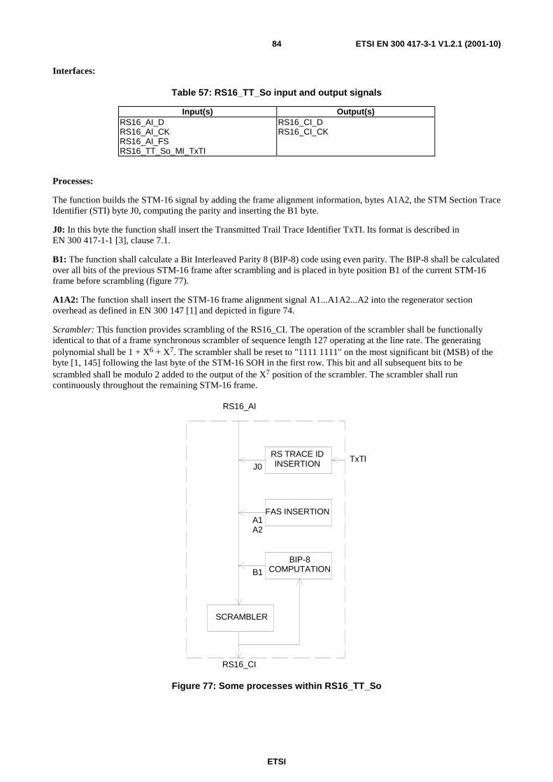
ETSI
ETSI EN 300 417-3-1 V1.2.1 (2001-10)84
Interfaces:
Table 57: RS16_TT_So input and output signals
Input(s) Output(s) RS16_AI_D RS16_AI_CK RS16_AI_FS RS16_TT_So_MI_TxTI
RS16_CI_D RS16_CI_CK
Processes:
The function builds the STM-16 signal by adding the frame alignment information, bytes A1A2, the STM Section Trace Identifier (STI) byte J0, computing the parity and inserting the B1 byte.
J0: In this byte the function shall insert the Transmitted Trail Trace Identifier TxTI. Its format is described in EN 300 417-1-1 [3], clause 7.1.
B1: The function shall calculate a Bit Interleaved Parity 8 (BIP-8) code using even parity. The BIP-8 shall be calculated over all bits of the previous STM-16 frame after scrambling and is placed in byte position B1 of the current STM-16 frame before scrambling (figure 77).
A1A2: The function shall insert the STM-16 frame alignment signal A1...A1A2...A2 into the regenerator section overhead as defined in EN 300 147 [1] and depicted in figure 74.
Scrambler: This function provides scrambling of the RS16_CI. The operation of the scrambler shall be functionally identical to that of a frame synchronous scrambler of sequence length 127 operating at the line rate. The generating polynomial shall be 1 + X6 + X7. The scrambler shall be reset to "1111 1111" on the most significant bit (MSB) of the byte [1, 145] following the last byte of the STM-16 SOH in the first row. This bit and all subsequent bits to be scrambled shall be modulo 2 added to the output of the X7 position of the scrambler. The scrambler shall run continuously throughout the remaining STM-16 frame.
SCRAMBLER
BIP-8COMPUTATIONB1
RS16_CI
RS TRACE IDINSERTIONJ0
FAS INSERTION
RS16_AI
A1A2
TxTI
Figure 77: Some processes within RS16_TT_So

ETSI
ETSI EN 300 417-3-1 V1.2.1 (2001-10)85
Defects: None.
Consequent Actions: None.
Defect Correlations: None.
Performance Monitoring: None.
8.2.2 STM-16 Regenerator Section Trail Termination Sink RS16_TT_Sk
Symbol:
RS16
RS16_AI
RS16_CI
RS16_TT_Sk_MI
Figure 78: RS16_TT_Sk symbol
Interfaces:
Table 58: RS16_TT_Sk input and output signals
Input(s) Output(s) RS16_CI_D RS16_CI_CK RS16_CI_FS RS16_CI_SSF RS16_TT_Sk_MI_ExTI RS16_TT_Sk_MI_TPmode RS16_TT_Sk_MI_TIMdis RS16_TT_Sk_MI_ExTImode RS16_TT_Sk_MI_1second
RS16_AI_D RS16_AI_CK RS16_AI_FS RS16_AI_TSF RS16_TT_Sk_MI_AcTI RS16_TT_Sk_MI_cTIM RS16_TT_Sk_MI_pN_EBC RS16_TT_Sk_MI_pN_DS
Processes:
This function monitors the STM-16 signal for RS errors, and recovers the RS trail termination status. It extracts the payload independent overhead bytes (J0, B1) from the RS16 layer Characteristic Information:
Descrambling: The function shall descramble the incoming STM-16 signal. The operation of the descrambler shall be functionally identical to that of a scrambler in RS16_TT_So.
B1: Even bit parity is computed for each bit n of every byte of the preceding scrambled STM-16 frame and compared with bit n of B1 recovered from the current frame (n = 1 to 8 inclusive) (figure 79). A difference between the computed and recovered B1 values is taken as evidence of one or more errors (nN_B) in the computation block.
J0: The Received Trail Trace Identifier RxTI shall be recovered from the J0 byte and shall be made available as AcTI for network management purposes. The application and acceptance and mismatch detection process shall be performed as specified in EN 300 417-1-1 [3], clauses 7.1 and 8.2.1.3.
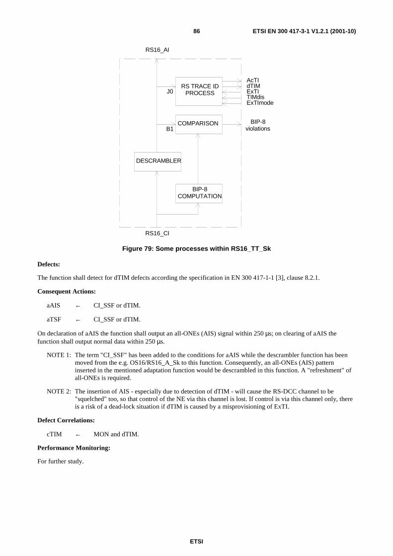
ETSI
ETSI EN 300 417-3-1 V1.2.1 (2001-10)86
DESCRAMBLER
BIP-8COMPUTATION
B1
RS TRACE IDPROCESSJ0
RS16_CI
COMPARISON BIP-8violations
AcTIdTIMExTI
RS16_AI
TIMdisExTImode
Figure 79: Some processes within RS16_TT_Sk
Defects:
The function shall detect for dTIM defects according the specification in EN 300 417-1-1 [3], clause 8.2.1.
Consequent Actions:
aAIS ← CI_SSF or dTIM.
aTSF ← CI_SSF or dTIM.
On declaration of aAIS the function shall output an all-ONEs (AIS) signal within 250 µs; on clearing of aAIS the function shall output normal data within 250 µs.
NOTE 1: The term "CI_SSF" has been added to the conditions for aAIS while the descrambler function has been moved from the e.g. OS16/RS16_A_Sk to this function. Consequently, an all-ONEs (AIS) pattern inserted in the mentioned adaptation function would be descrambled in this function. A "refreshment" of all-ONEs is required.
NOTE 2: The insertion of AIS - especially due to detection of dTIM - will cause the RS-DCC channel to be "squelched" too, so that control of the NE via this channel is lost. If control is via this channel only, there is a risk of a dead-lock situation if dTIM is caused by a misprovisioning of ExTI.
Defect Correlations:
cTIM ← MON and dTIM.
Performance Monitoring:
For further study.
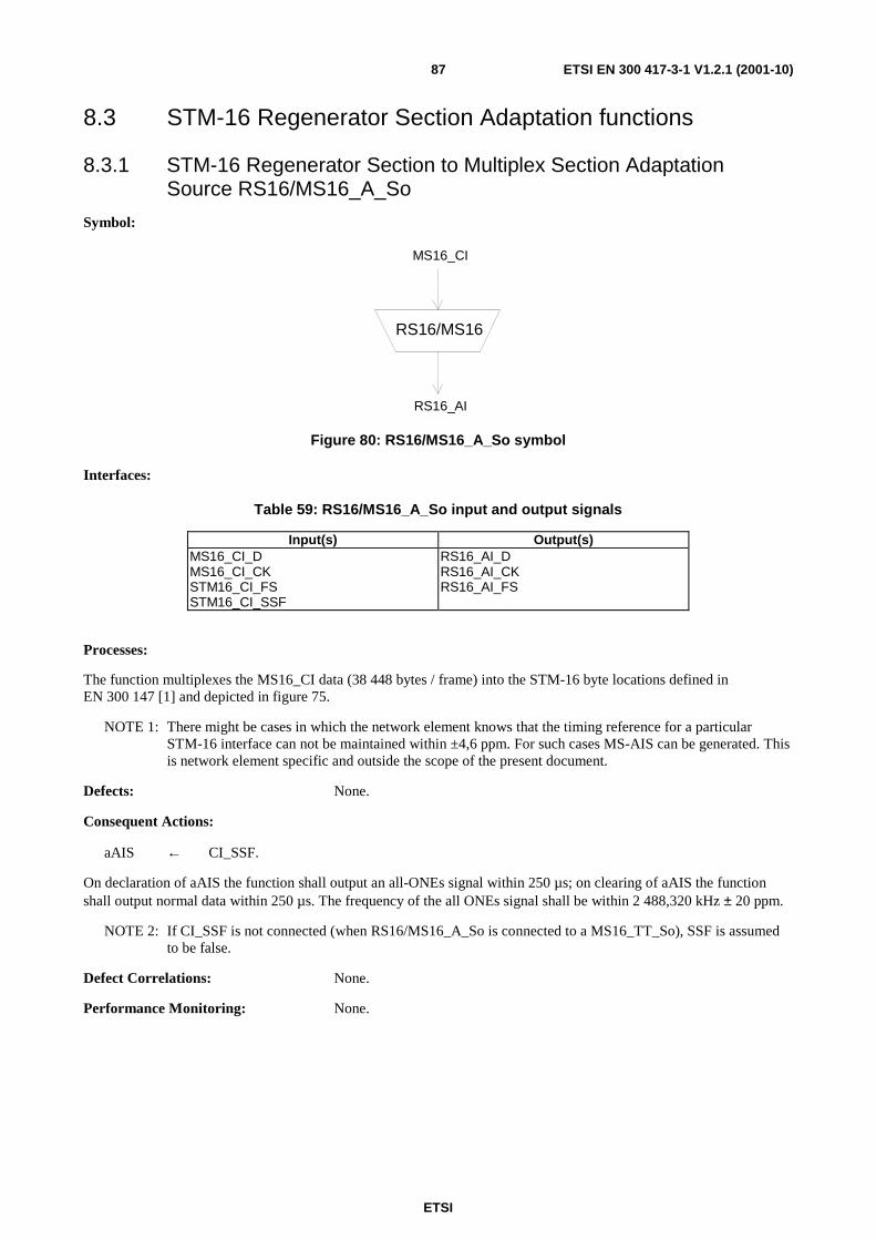
ETSI
ETSI EN 300 417-3-1 V1.2.1 (2001-10)87
8.3 STM-16 Regenerator Section Adaptation functions
8.3.1 STM-16 Regenerator Section to Multiplex Section Adaptation Source RS16/MS16_A_So
Symbol:
RS16/MS16
MS16_CI
RS16_AI
Figure 80: RS16/MS16_A_So symbol
Interfaces:
Table 59: RS16/MS16_A_So input and output signals
Input(s) Output(s) MS16_CI_D MS16_CI_CK STM16_CI_FS STM16_CI_SSF
RS16_AI_D RS16_AI_CK RS16_AI_FS
Processes:
The function multiplexes the MS16_CI data (38 448 bytes / frame) into the STM-16 byte locations defined in EN 300 147 [1] and depicted in figure 75.
NOTE 1: There might be cases in which the network element knows that the timing reference for a particular STM-16 interface can not be maintained within ±4,6 ppm. For such cases MS-AIS can be generated. This is network element specific and outside the scope of the present document.
Defects: None.
Consequent Actions:
aAIS ← CI_SSF.
On declaration of aAIS the function shall output an all-ONEs signal within 250 µs; on clearing of aAIS the function shall output normal data within 250 µs. The frequency of the all ONEs signal shall be within 2 488,320 kHz ± 20 ppm.
NOTE 2: If CI_SSF is not connected (when RS16/MS16_A_So is connected to a MS16_TT_So), SSF is assumed to be false.
Defect Correlations: None.
Performance Monitoring: None.
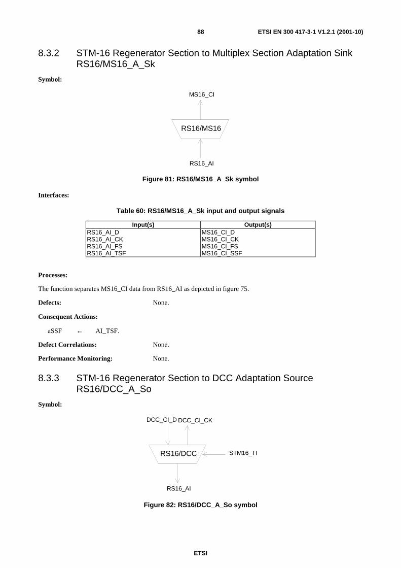
ETSI
ETSI EN 300 417-3-1 V1.2.1 (2001-10)88
8.3.2 STM-16 Regenerator Section to Multiplex Section Adaptation Sink RS16/MS16_A_Sk
Symbol:
RS16/MS16
MS16_CI
RS16_AI
Figure 81: RS16/MS16_A_Sk symbol
Interfaces:
Table 60: RS16/MS16_A_Sk input and output signals
Input(s) Output(s) RS16_AI_D RS16_AI_CK RS16_AI_FS RS16_AI_TSF
MS16_CI_D MS16_CI_CK MS16_CI_FS MS16_CI_SSF
Processes:
The function separates MS16_CI data from RS16_AI as depicted in figure 75.
Defects: None.
Consequent Actions:
aSSF ← AI_TSF.
Defect Correlations: None.
Performance Monitoring: None.
8.3.3 STM-16 Regenerator Section to DCC Adaptation Source RS16/DCC_A_So
Symbol:
RS16/DCC
DCC_CI_D
RS16_AI
STM16_TI
DCC_CI_CK
Figure 82: RS16/DCC_A_So symbol
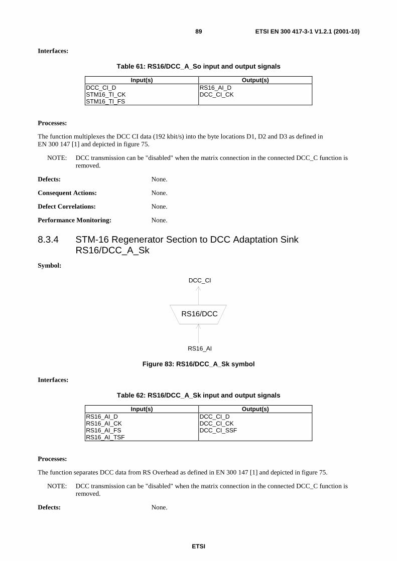
ETSI
ETSI EN 300 417-3-1 V1.2.1 (2001-10)89
Interfaces:
Table 61: RS16/DCC_A_So input and output signals
Input(s) Output(s) DCC_CI_D STM16_TI_CK STM16_TI_FS
RS16_AI_D DCC_CI_CK
Processes:
The function multiplexes the DCC CI data (192 kbit/s) into the byte locations D1, D2 and D3 as defined in EN 300 147 [1] and depicted in figure 75.
NOTE: DCC transmission can be "disabled" when the matrix connection in the connected DCC_C function is removed.
Defects: None.
Consequent Actions: None.
Defect Correlations: None.
Performance Monitoring: None.
8.3.4 STM-16 Regenerator Section to DCC Adaptation Sink RS16/DCC_A_Sk
Symbol:
RS16/DCC
DCC_CI
RS16_AI
Figure 83: RS16/DCC_A_Sk symbol
Interfaces:
Table 62: RS16/DCC_A_Sk input and output signals
Input(s) Output(s) RS16_AI_D RS16_AI_CK RS16_AI_FS RS16_AI_TSF
DCC_CI_D DCC_CI_CK DCC_CI_SSF
Processes:
The function separates DCC data from RS Overhead as defined in EN 300 147 [1] and depicted in figure 75.
NOTE: DCC transmission can be "disabled" when the matrix connection in the connected DCC_C function is removed.
Defects: None.

ETSI
ETSI EN 300 417-3-1 V1.2.1 (2001-10)90
Consequent Actions:
aSSF ← AI_TSF.
Defect Correlations: None.
Performance Monitoring: None.
8.3.5 STM-16 Regenerator Section to P0s Adaptation Source RS16/P0s_A_So/N
Symbol:
RS16/P0s-N
P0s_CI
RS16_AI
STM16_TI
N=E1,F1
Figure 84: RS16/P0s_A_So symbol
Interfaces:
Table 63: RS16/P0s_A_So input and output signals
Input(s) Output(s) P0s_CI_D P0s_CI_CK P0s_CI_FS MS16_TI_CK MS16_TI_FS
RS16_AI_D
Processes:
This function provides the multiplexing of a 64 kbit/s orderwire or user channel information stream into the RS16_AI using slip buffering. It takes P0s_CI, defined in EN 300 166 [2] as an octet structured bit-stream with a synchronous bit rate of 64 kbit/s, present at its input and inserts it into the RSOH byte E1 or F1 as defined in EN 300 147 [1] and depicted in figure 75.
NOTE: Any frequency deviation between the 64 kbit/s signal and the associated STM-16 signal leads to octet slips.
Frequency justification and bitrate adaptation: The function shall provide an elastic store (slip buffer) process. The data signal shall be written into the store under control of the associated input clock. The data shall be read out of the store under control of the STM-16 clock, frame position (STM16_TI), and justification decisions.
Each justification decision results in a corresponding negative / positive justification action. Upon a positive justification action, the reading of one 64 kbit/s octet (8 bits) shall be cancelled once. Upon a negative justification action, the same 64 kbit/s octet (8 bits) shall be read out a second time.
Buffer size: The elastic store (slip buffer) shall accommodate at least 18 µs of wander without introducing errors.
64 kbit/s timeslot: The adaptation source function has access to a specific 64 kbit/s channel of the RS access point. The specific 64 kbit/s channel is defined by the parameter N (N = E1, F1).
Defects: None.
Consequent Actions: None.

ETSI
ETSI EN 300 417-3-1 V1.2.1 (2001-10)91
Defect Correlations: None.
Performance Monitoring: None.
8.3.6 STM-16 Regenerator Section to P0s Adaptation Sink RS16/P0s_A_Sk/N
Symbol:
RS16/P0s-N
P0s_CI
RS16_AI
N=E1,F1
Figure 85: RS16/P0s_A_Sk symbol
Interfaces:
Table 64: RS16/P0s_A_Sk input and output signals
Input(s) Output(s) RS16_AI_D RS16_AI_CK RS16_AI_FS RS16_AI_TSF
P0s_CI_Sk_D P0s_CI_Sk_CK P0s_CI_FS P0s_CI_SSF
Processes:
The function separates P0s data from RS Overhead byte E1 or F1 as defined in EN 300 147 [1] and depicted in figure 75.
Data latching and smoothing process: The function shall provide a data latching and smoothing function. Each 8-bit octet received shall be written and latched into a data store under the control of the STM-16 signal clock. The eight data bits shall then be read out of the store using a nominal 64 kHz clock which may be derived directly from the incoming STM-16 signal clock (e.g. 2 488 320 kHz divided by a factor of 38 880).
64 kbit/s timeslot: The adaptation sink function has access to a specific 64 kbit/s of the RS access point. The specific 64 kbit/s is defined by the parameter N (N = E1, F1).
Defects: None.
Consequent Actions:
aSSF ← AI_TSF.
aAIS ← AI_TSF.
On declaration of aAIS the function shall output an all-ONEs (AIS) signal - complying with the frequency limits for this signal (a bit rate in range 64 kbit/s ± 100 ppm) - within 1 ms; on clearing of aAIS the function shall output normal data within 1 ms.
Defect Correlations: None.
Performance Monitoring: None.
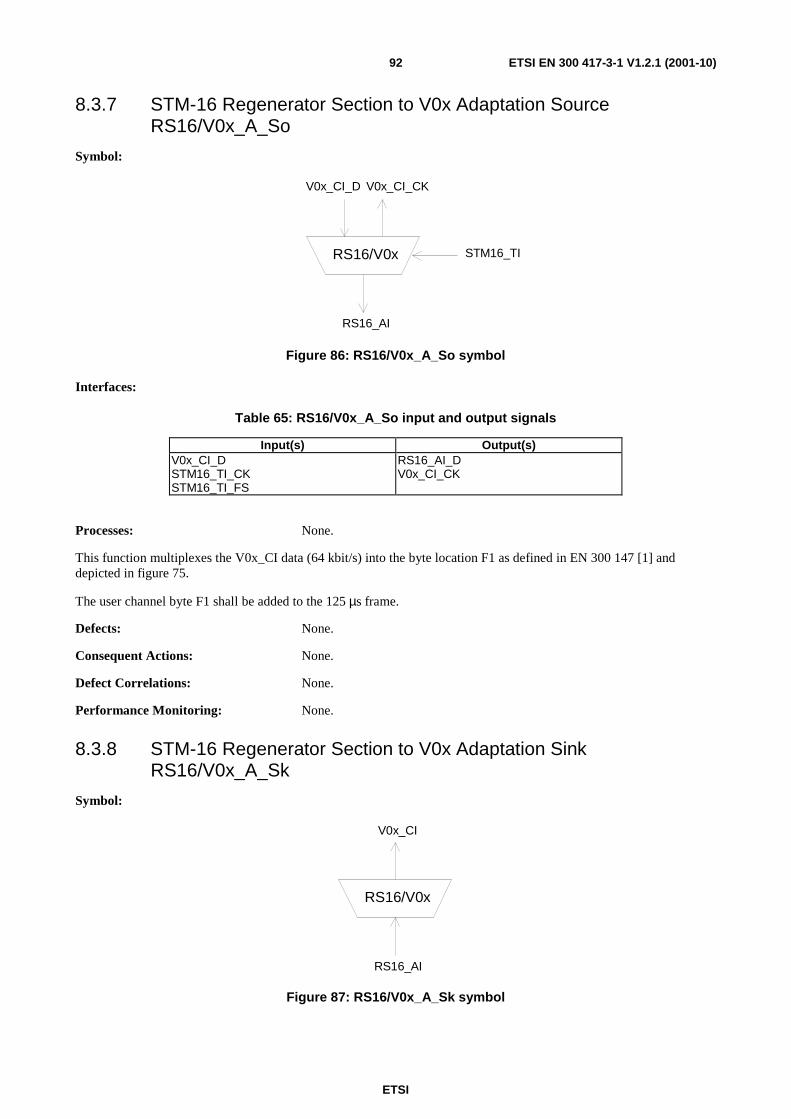
ETSI
ETSI EN 300 417-3-1 V1.2.1 (2001-10)92
8.3.7 STM-16 Regenerator Section to V0x Adaptation Source RS16/V0x_A_So
Symbol:
RS16/V0x
RS16_AI
STM16_TI
V0x_CI_D V0x_CI_CK
Figure 86: RS16/V0x_A_So symbol
Interfaces:
Table 65: RS16/V0x_A_So input and output signals
Input(s) Output(s) V0x_CI_D STM16_TI_CK STM16_TI_FS
RS16_AI_D V0x_CI_CK
Processes: None.
This function multiplexes the V0x_CI data (64 kbit/s) into the byte location F1 as defined in EN 300 147 [1] and depicted in figure 75.
The user channel byte F1 shall be added to the 125 µs frame.
Defects: None.
Consequent Actions: None.
Defect Correlations: None.
Performance Monitoring: None.
8.3.8 STM-16 Regenerator Section to V0x Adaptation Sink RS16/V0x_A_Sk
Symbol:
RS16/V0x
V0x_CI
RS16_AI
Figure 87: RS16/V0x_A_Sk symbol
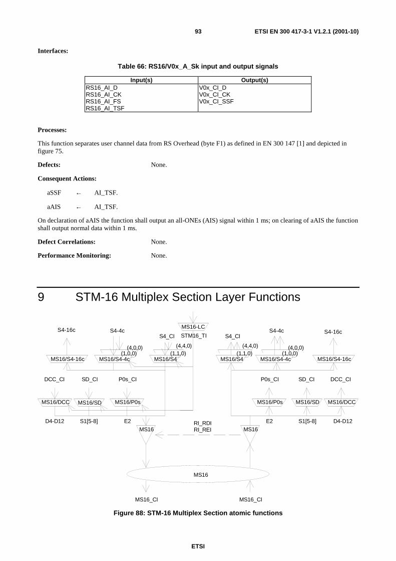
ETSI
ETSI EN 300 417-3-1 V1.2.1 (2001-10)93
Interfaces:
Table 66: RS16/V0x_A_Sk input and output signals
Input(s) Output(s) RS16_AI_D RS16_AI_CK RS16_AI_FS RS16_AI_TSF
V0x_CI_D V0x_CI_CK V0x_CI_SSF
Processes:
This function separates user channel data from RS Overhead (byte F1) as defined in EN 300 147 [1] and depicted in figure 75.
Defects: None.
Consequent Actions:
aSSF ← AI_TSF.
aAIS ← AI_TSF.
On declaration of aAIS the function shall output an all-ONEs (AIS) signal within 1 ms; on clearing of aAIS the function shall output normal data within 1 ms.
Defect Correlations: None.
Performance Monitoring: None.
9 STM-16 Multiplex Section Layer Functions
MS16 MS16
MS16_CI MS16_CI
MS16/SD MS16/SDMS16/P0s
P0s_CI
STM16_TI
MS16/P0s
P0s_CI
E2 E2
SD_CISD_CI
MS16/DCC
DCC_CI
S1[5-8] D4-D12
MS16/DCC
DCC_CI
D4-D12 S1[5-8] RI_RDIRI_REI
S4_CI
MS16/S4
S4_CI
(1,1,0)(4,4,0)
S4-4c
MS16/S4(1,1,0)
(4,4,0)
S4-4c
MS16/S4-4c(1,0,0)
(4,0,0)
MS16/S4-4c(1,0,0)
(4,0,0)
MS16-LC
MS16
MS16/S4-16cMS16/S4-16c
S4-16cS4-16c
Figure 88: STM-16 Multiplex Section atomic functions
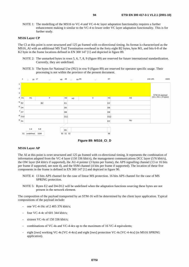
ETSI
ETSI EN 300 417-3-1 V1.2.1 (2001-10)94
NOTE 1: The modelling of the MS16 to VC-4 and VC-4-4c layer adaptation functionality requires a further enhancement making it similar to the VC-4 to lower order VC layer adaptation functionality. This is for further study.
MS16 Layer CP
The CI at this point is octet structured and 125 µs framed with co-directional timing. Its format is characterized as the MS16_AI with an additional MS Trail Termination overhead in the forty eight B2 bytes, byte M1, and bits 6-8 of the K2 byte in the frame locations defined in EN 300 147 [1] and depicted in figure 89.
NOTE 2: The unmarked bytes in rows 5, 6, 7, 8, 9 (figure 89) are reserved for future international standardization. Currently, they are undefined.
NOTE 3: The bytes for National Use (NU) in row 9 (figure 89) are reserved for operator specific usage. Their processing is not within the province of the present document.
B2
D4
D7
D10
S1
B2 K1
D5
D8
D11
M1
K2
D6
D9
D12
E2
1
2
3
4
5
6
7
8
9
H1 H1 H2 H3 H3
NU
'1'Y
1 17 49 65 97 144 145 4320
STM-16 payload(16 x 261 x 9 bytes)
50 51 52 96
H2
4816 64... ... ... ... ...
SSMundefined
1-4 5-8
S1
Figure 89: MS16_CI_D
MS16 Layer AP
The AI at this point is octet structured and 125 µs framed with co-directional timing. It represents the combination of information adapted from the VC-4 layer (150 336 kbit/s), the management communications DCC layer (576 kbit/s), the OW layer (64 kbit/s if supported), the AU-4 pointer (3 bytes per frame), the APS signalling channel (13 or 16 bits per frame if supported, see note 4), and the SSM channel (4 bits per frame if supported). The location of these five components in the frame is defined in EN 300 147 [1] and depicted in figure 90.
NOTE 4: 13 bits APS channel for the case of linear MS protection. 16 bits APS channel for the case of MS SPRING protection.
NOTE 5: Bytes E2 and D4-D12 will be undefined when the adaptation functions sourcing these bytes are not present in the network element.
The composition of the payload transported by an STM-16 will be determined by the client layer application. Typical compositions of the payload include:
- one VC-4-16c of 2 405 376 kbit/s;
- four VC-4-4c of 601 344 kbit/s;
- sixteen VC-4s of 150 336 kbit/s;
- combinations of VC-4s and VC-4-4cs up to the maximum of 16 VC-4 equivalents;
- eight [two] working VC-4s [VC-4-4cs] and eight [two] protection VC-4s [VC-4-4cs] (in MS16 SPRING application).
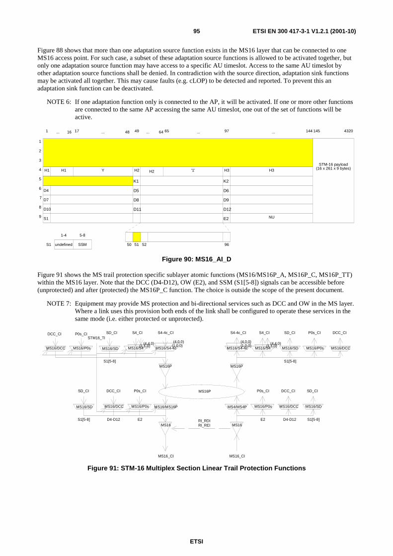
ETSI
ETSI EN 300 417-3-1 V1.2.1 (2001-10)95
Figure 88 shows that more than one adaptation source function exists in the MS16 layer that can be connected to one MS16 access point. For such case, a subset of these adaptation source functions is allowed to be activated together, but only one adaptation source function may have access to a specific AU timeslot. Access to the same AU timeslot by other adaptation source functions shall be denied. In contradiction with the source direction, adaptation sink functions may be activated all together. This may cause faults (e.g. cLOP) to be detected and reported. To prevent this an adaptation sink function can be deactivated.
NOTE 6: If one adaptation function only is connected to the AP, it will be activated. If one or more other functions are connected to the same AP accessing the same AU timeslot, one out of the set of functions will be active.
D4
D7
D10
S1
K1
D5
D8
D11
K2
D6
D9
D12
E2
1
2
3
4
5
6
7
8
9
H1 H1 H2 H3 H3
NU
'1'Y
1 17 49 65 97 144 145 4320
STM-16 payload(16 x 261 x 9 bytes)
50 51 52 96
H2
4816 64... ... ... ... ...
SSMundefined
1-4 5-8
S1
Figure 90: MS16_AI_D
Figure 91 shows the MS trail protection specific sublayer atomic functions (MS16/MS16P_A, MS16P_C, MS16P_TT) within the MS16 layer. Note that the DCC (D4-D12), OW (E2), and SSM (S1[5-8]) signals can be accessible before (unprotected) and after (protected) the MS16P_C function. The choice is outside the scope of the present document.
NOTE 7: Equipment may provide MS protection and bi-directional services such as DCC and OW in the MS layer. Where a link uses this provision both ends of the link shall be configured to operate these services in the same mode (i.e. either protected or unprotected).
MS16
MS16/MS16P
MS16
MS4/MS4P
MS16P
MS16_CI MS16_CI
MS16/P0s
P0s_CI
STM16_TI
MS16/P0s
P0s_CI
E2 E2
MS16/DCC
DCC_CI
D4-D12
MS16/DCC
DCC_CI
D4-D12 RI_RDIRI_REI
MS16/S4-4c
S4-4c_CI
MS16/S4-4c
S4-4c_CI
MS16/SD
SD_CI
S1[5-8]MS16P MS16P
S4_CI
MS16/S4(1,1,0)(4,4,0)
MS16/P0sMS16/DCC
P0s_CIDCC_CI
MS16/P0s MS16/DCC
P0s_CI DCC_CI
MS16/SD
S1[5-8]
SD_CI
MS16/SD
S1[5-8]
SD_CI
MS16/SD
SD_CI
S1[5-8]
S4_CI
MS16/S4(1,1,0)(4,4,0) (4,0,0)
(1,0,0)(4,0,0)(1,0,0)
Figure 91: STM-16 Multiplex Section Linear Trail Protection Functions
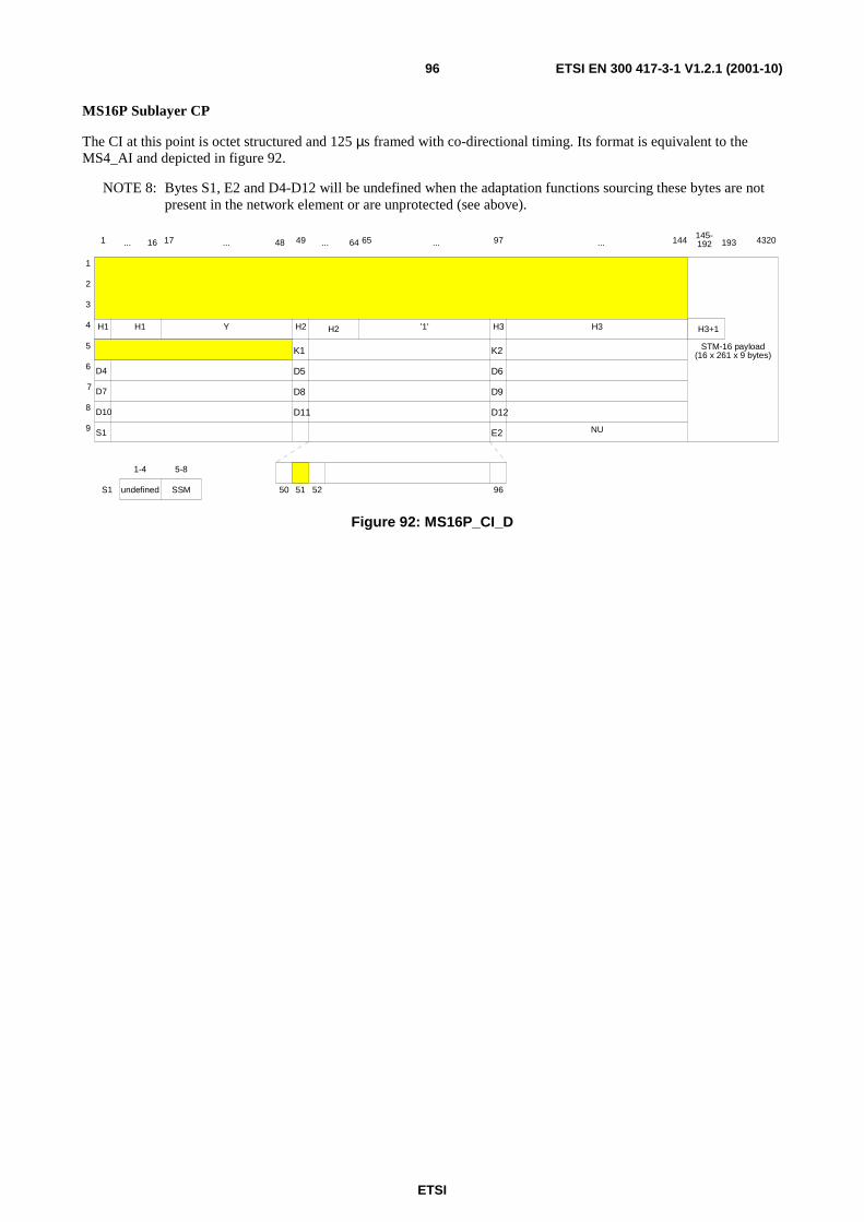
ETSI
ETSI EN 300 417-3-1 V1.2.1 (2001-10)96
MS16P Sublayer CP
The CI at this point is octet structured and 125 µs framed with co-directional timing. Its format is equivalent to the MS4_AI and depicted in figure 92.
NOTE 8: Bytes S1, E2 and D4-D12 will be undefined when the adaptation functions sourcing these bytes are not present in the network element or are unprotected (see above).
D4
D7
D10
S1
K1
D5
D8
D11
K2
D6
D9
D12
E2
1
2
3
4
5
6
7
8
9
H1 H1 H2 H3 H3
NU
'1'Y
1 17 49 65 97 144 145-192 4320
STM-16 payload(16 x 261 x 9 bytes)
50 51 52 96
H2
4816 64... ... ... ... ...
SSMundefined
1-4 5-8
S1
H3+1
193
Figure 92: MS16P_CI_D
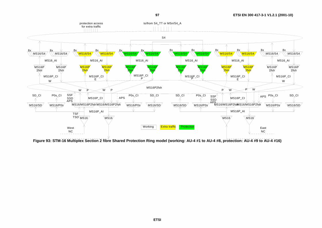
ETSI
ETSI EN 300 417-3-1 V1.2.1 (2001-10)97
MS16/MS16P2fsh
MS16
MS16P2fsh
APS
SSFSSD
TSFTSD
NCWest
S4
to/from S4_TT or MSn/S4_A
W P
MS16/MS16P2fsh
MS16
APS
NCEast
WP
8x 8x8x 8x
protection accessfor extra traffic
MS16/MS16P2fsh
MS16
MS16/MS16P2fsh
MS16
8x
MS16P2fsh
8xMS16/S4
MS16P2fsh
MS16/S4 MS16/S4
MS16P2fsh
MS16P2fsh
MS16P2fsh
MS16P2fsh
MS16/S4MS16/S4 MS16/S4
WE P
MS16P2fsh
MS16/S4
MS16P2fsh
MS16/S4MS16/S4
MS16P2fsh
MS16P2fsh
MS16P2fsh
MS16P2fsh
MS16/S4 MS16/S4MS16/S48x 8x8x 8x8x8x
MS16P_AI
MS16P_CI APS MS16P_CI
MS16P_CI MS16P_CI MS16P_CI MS16P_CI MS16P_CI MS16P_CI
W P P W
MS16P_AI
P EW
Working Extra traffic Protection
MS16_AI MS16_AI MS16_AI MS16_AI MS16_AI MS16_AI
MS16/P0sMS16/SD
P0s_CISD_CI
MS16/P0sMS16/SD
P0s_CISD_CI
MS16/P0s MS16/SD
P0s_CI SD_CI
MS16/P0s MS16/SD
P0s_CI SD_CI
APS
SSFSSD
Figure 93: STM-16 Multiplex Section 2 fibre Shared Protection Ring model (working: AU-4 #1 to AU-4 #8, protection: AU-4 #9 to AU-4 #16)
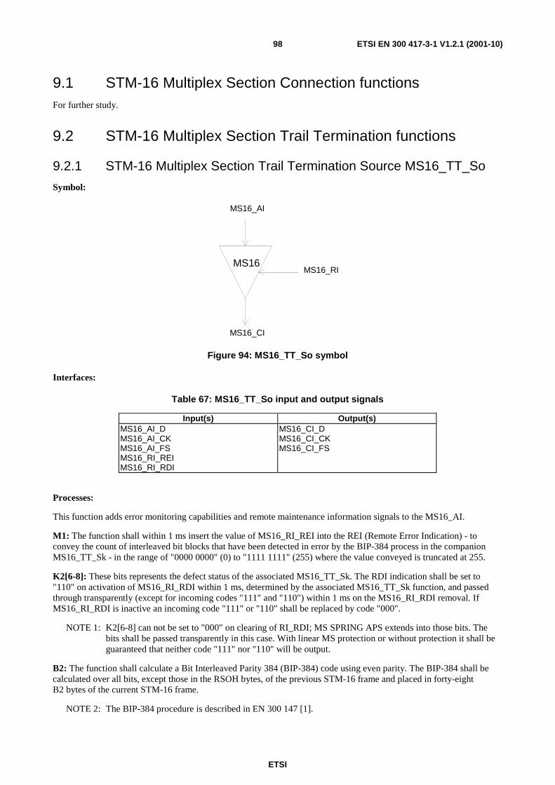
ETSI
ETSI EN 300 417-3-1 V1.2.1 (2001-10)98
9.1 STM-16 Multiplex Section Connection functions For further study.
9.2 STM-16 Multiplex Section Trail Termination functions
9.2.1 STM-16 Multiplex Section Trail Termination Source MS16_TT_So
Symbol:
MS16
MS16_AI
MS16_CI
MS16_RI
Figure 94: MS16_TT_So symbol
Interfaces:
Table 67: MS16_TT_So input and output signals
Input(s) Output(s) MS16_AI_D MS16_AI_CK MS16_AI_FS MS16_RI_REI MS16_RI_RDI
MS16_CI_D MS16_CI_CK MS16_CI_FS
Processes:
This function adds error monitoring capabilities and remote maintenance information signals to the MS16_AI.
M1: The function shall within 1 ms insert the value of MS16_RI_REI into the REI (Remote Error Indication) - to convey the count of interleaved bit blocks that have been detected in error by the BIP-384 process in the companion MS16_TT_Sk - in the range of "0000 0000" (0) to "1111 1111" (255) where the value conveyed is truncated at 255.
K2[6-8]: These bits represents the defect status of the associated MS16_TT_Sk. The RDI indication shall be set to "110" on activation of MS16_RI_RDI within 1 ms, determined by the associated MS16_TT_Sk function, and passed through transparently (except for incoming codes "111" and "110") within 1 ms on the MS16_RI_RDI removal. If MS16_RI_RDI is inactive an incoming code "111" or "110" shall be replaced by code "000".
NOTE 1: K2[6-8] can not be set to "000" on clearing of RI_RDI; MS SPRING APS extends into those bits. The bits shall be passed transparently in this case. With linear MS protection or without protection it shall be guaranteed that neither code "111" nor "110" will be output.
B2: The function shall calculate a Bit Interleaved Parity 384 (BIP-384) code using even parity. The BIP-384 shall be calculated over all bits, except those in the RSOH bytes, of the previous STM-16 frame and placed in forty-eight B2 bytes of the current STM-16 frame.
NOTE 2: The BIP-384 procedure is described in EN 300 147 [1].
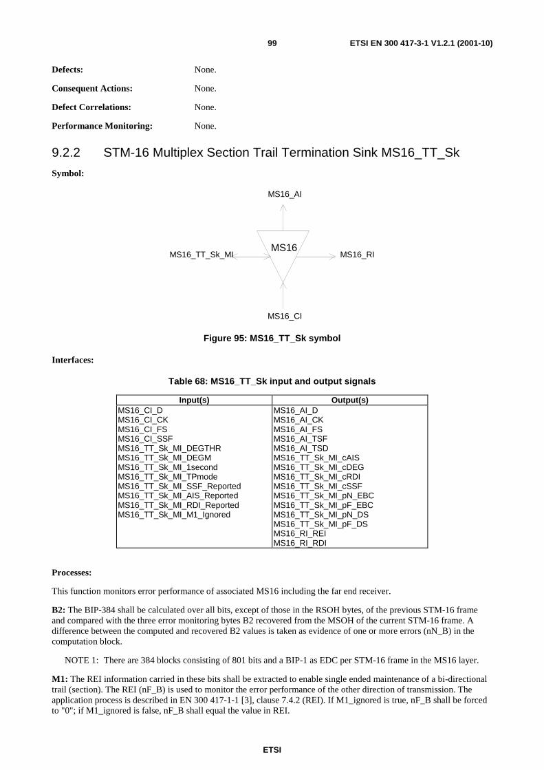
ETSI
ETSI EN 300 417-3-1 V1.2.1 (2001-10)99
Defects: None.
Consequent Actions: None.
Defect Correlations: None.
Performance Monitoring: None.
9.2.2 STM-16 Multiplex Section Trail Termination Sink MS16_TT_Sk
Symbol:
MS16
MS16_AI
MS16_CI
MS16_TT_Sk_MI MS16_RI
Figure 95: MS16_TT_Sk symbol
Interfaces:
Table 68: MS16_TT_Sk input and output signals
Input(s) Output(s) MS16_CI_D MS16_CI_CK MS16_CI_FS MS16_CI_SSF MS16_TT_Sk_MI_DEGTHR MS16_TT_Sk_MI_DEGM MS16_TT_Sk_MI_1second MS16_TT_Sk_MI_TPmode MS16_TT_Sk_MI_SSF_Reported MS16_TT_Sk_MI_AIS_Reported MS16_TT_Sk_MI_RDI_Reported MS16_TT_Sk_MI_M1_Ignored
MS16_AI_D MS16_AI_CK MS16_AI_FS MS16_AI_TSF MS16_AI_TSD MS16_TT_Sk_MI_cAIS MS16_TT_Sk_MI_cDEG MS16_TT_Sk_MI_cRDI MS16_TT_Sk_MI_cSSF MS16_TT_Sk_MI_pN_EBC MS16_TT_Sk_MI_pF_EBC MS16_TT_Sk_MI_pN_DS MS16_TT_Sk_MI_pF_DS MS16_RI_REI MS16_RI_RDI
Processes:
This function monitors error performance of associated MS16 including the far end receiver.
B2: The BIP-384 shall be calculated over all bits, except of those in the RSOH bytes, of the previous STM-16 frame and compared with the three error monitoring bytes B2 recovered from the MSOH of the current STM-16 frame. A difference between the computed and recovered B2 values is taken as evidence of one or more errors (nN_B) in the computation block.
NOTE 1: There are 384 blocks consisting of 801 bits and a BIP-1 as EDC per STM-16 frame in the MS16 layer.
M1: The REI information carried in these bits shall be extracted to enable single ended maintenance of a bi-directional trail (section). The REI (nF_B) is used to monitor the error performance of the other direction of transmission. The application process is described in EN 300 417-1-1 [3], clause 7.4.2 (REI). If M1_ignored is true, nF_B shall be forced to "0"; if M1_ignored is false, nF_B shall equal the value in REI.
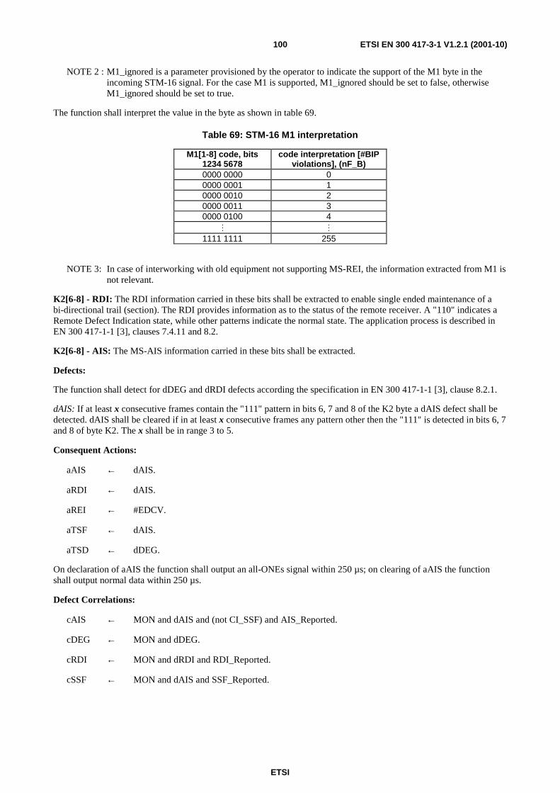
ETSI
ETSI EN 300 417-3-1 V1.2.1 (2001-10)100
NOTE 2 : M1_ignored is a parameter provisioned by the operator to indicate the support of the M1 byte in the incoming STM-16 signal. For the case M1 is supported, M1_ignored should be set to false, otherwise M1_ignored should be set to true.
The function shall interpret the value in the byte as shown in table 69.
Table 69: STM-16 M1 interpretation
M1[1-8] code, bits 1234 5678
code interpretation [#BIP violations], (nF_B)
0000 0000 0 0000 0001 1 0000 0010 2 0000 0011 3 0000 0100 4
M M 1111 1111 255
NOTE 3: In case of interworking with old equipment not supporting MS-REI, the information extracted from M1 is not relevant.
K2[6-8] - RDI: The RDI information carried in these bits shall be extracted to enable single ended maintenance of a bi-directional trail (section). The RDI provides information as to the status of the remote receiver. A "110" indicates a Remote Defect Indication state, while other patterns indicate the normal state. The application process is described in EN 300 417-1-1 [3], clauses 7.4.11 and 8.2.
K2[6-8] - AIS: The MS-AIS information carried in these bits shall be extracted.
Defects:
The function shall detect for dDEG and dRDI defects according the specification in EN 300 417-1-1 [3], clause 8.2.1.
dAIS: If at least x consecutive frames contain the "111" pattern in bits 6, 7 and 8 of the K2 byte a dAIS defect shall be detected. dAIS shall be cleared if in at least x consecutive frames any pattern other then the "111" is detected in bits 6, 7 and 8 of byte K2. The x shall be in range 3 to 5.
Consequent Actions:
aAIS ← dAIS.
aRDI ← dAIS.
aREI ← #EDCV.
aTSF ← dAIS.
aTSD ← dDEG.
On declaration of aAIS the function shall output an all-ONEs signal within 250 µs; on clearing of aAIS the function shall output normal data within 250 µs.
Defect Correlations:
cAIS ← MON and dAIS and (not CI_SSF) and AIS_Reported.
cDEG ← MON and dDEG.
cRDI ← MON and dRDI and RDI_Reported.
cSSF ← MON and dAIS and SSF_Reported.
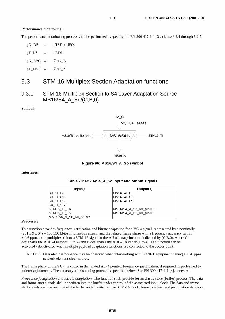
ETSI
ETSI EN 300 417-3-1 V1.2.1 (2001-10)101
Performance monitoring:
The performance monitoring process shall be performed as specified in EN 300 417-1-1 [3], clause 8.2.4 through 8.2.7.
pN_DS ← aTSF or dEQ.
pF_DS ← dRDI.
pN_EBC ← Σ nN_B.
pF_EBC ← Σ nF_B.
9.3 STM-16 Multiplex Section Adaptation functions
9.3.1 STM-16 Multiplex Section to S4 Layer Adaptation Source MS16/S4_A_So/(C,B,0)
Symbol:
MS16/S4-N
S4_CI
MS16_AI
MS16/S4_A_So_MI STM16_TI
N=(1,1,0) .. (4,4,0)
Figure 96: MS16/S4_A_So symbol
Interfaces:
Table 70: MS16/S4_A_So input and output signals
Input(s) Output(s) S4_CI_D S4_CI_CK S4_CI_FS S4_CI_SSF STM16_TI_CK STM16_TI_FS MS16/S4_A_So_MI_Active
MS16_AI_D MS16_AI_CK MS16_AI_FS MS16/S4_A_So_MI_pPJE+ MS16/S4_A_So_MI_pPJE-
Processes:
This function provides frequency justification and bitrate adaptation for a VC-4 signal, represented by a nominally (261 x 9 x 64) = 150 336 kbit/s information stream and the related frame phase with a frequency accuracy within ± 4,6 ppm, to be multiplexed into a STM-16 signal at the AU tributary location indicated by (C,B,0), where C designates the AUG-4 number (1 to 4) and B designates the AUG-1 number (1 to 4). The function can be activated / deactivated when multiple payload adaptation functions are connected to the access point.
NOTE 1: Degraded performance may be observed when interworking with SONET equipment having a ± 20 ppm network element clock source.
The frame phase of the VC-4 is coded in the related AU-4 pointer. Frequency justification, if required, is performed by pointer adjustments. The accuracy of this coding process is specified below. See EN 300 417-4-1 [4], annex A.
Frequency justification and bitrate adaptation: The function shall provide for an elastic store (buffer) process. The data and frame start signals shall be written into the buffer under control of the associated input clock. The data and frame start signals shall be read out of the buffer under control of the STM-16 clock, frame position, and justification decision.
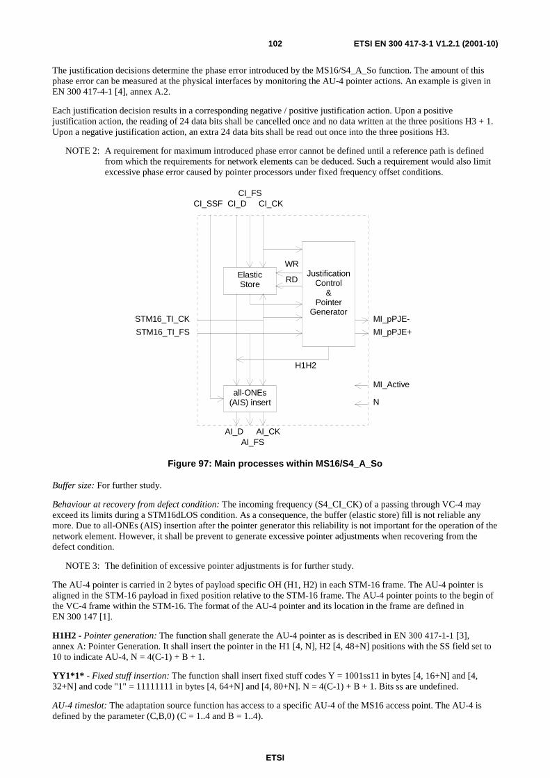
ETSI
ETSI EN 300 417-3-1 V1.2.1 (2001-10)102
The justification decisions determine the phase error introduced by the MS16/S4_A_So function. The amount of this phase error can be measured at the physical interfaces by monitoring the AU-4 pointer actions. An example is given in EN 300 417-4-1 [4], annex A.2.
Each justification decision results in a corresponding negative / positive justification action. Upon a positive justification action, the reading of 24 data bits shall be cancelled once and no data written at the three positions H3 + 1. Upon a negative justification action, an extra 24 data bits shall be read out once into the three positions H3.
NOTE 2: A requirement for maximum introduced phase error cannot be defined until a reference path is defined from which the requirements for network elements can be deduced. Such a requirement would also limit excessive phase error caused by pointer processors under fixed frequency offset conditions.
ElasticStore
JustificationControl
&Pointer
Generator
STM16_TI_FS
STM16_TI_CK
WR
RD
all-ONEs(AIS) insert
CI_SSF CI_DCI_FS
CI_CK
AI_DAI_FS
AI_CK
H1H2
MI_pPJE-
MI_pPJE+
MI_Active
N
Figure 97: Main processes within MS16/S4_A_So
Buffer size: For further study.
Behaviour at recovery from defect condition: The incoming frequency (S4_CI_CK) of a passing through VC-4 may exceed its limits during a STM16dLOS condition. As a consequence, the buffer (elastic store) fill is not reliable any more. Due to all-ONEs (AIS) insertion after the pointer generator this reliability is not important for the operation of the network element. However, it shall be prevent to generate excessive pointer adjustments when recovering from the defect condition.
NOTE 3: The definition of excessive pointer adjustments is for further study.
The AU-4 pointer is carried in 2 bytes of payload specific OH (H1, H2) in each STM-16 frame. The AU-4 pointer is aligned in the STM-16 payload in fixed position relative to the STM-16 frame. The AU-4 pointer points to the begin of the VC-4 frame within the STM-16. The format of the AU-4 pointer and its location in the frame are defined in EN 300 147 [1].
H1H2 - Pointer generation: The function shall generate the AU-4 pointer as is described in EN 300 417-1-1 [3], annex A: Pointer Generation. It shall insert the pointer in the H1 [4, N], H2 [4, 48+N] positions with the SS field set to 10 to indicate AU-4, N = 4(C-1) + B + 1.
YY1*1* - Fixed stuff insertion: The function shall insert fixed stuff codes Y = 1001ss11 in bytes [4, 16+N] and [4, 32+N] and code "1" = 11111111 in bytes [4, 64+N] and [4, 80+N]. N = 4(C-1) + B + 1. Bits ss are undefined.
AU-4 timeslot: The adaptation source function has access to a specific AU-4 of the MS16 access point. The AU-4 is defined by the parameter (C,B,0) (C = 1..4 and B = 1..4).
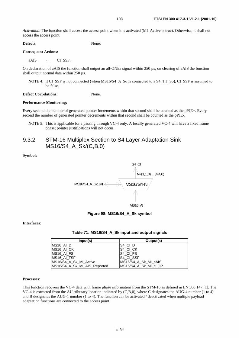
ETSI
ETSI EN 300 417-3-1 V1.2.1 (2001-10)103
Activation: The function shall access the access point when it is activated (MI_Active is true). Otherwise, it shall not access the access point.
Defects: None.
Consequent Actions:
aAIS ← CI_SSF.
On declaration of aAIS the function shall output an all-ONEs signal within 250 µs; on clearing of aAIS the function shall output normal data within 250 µs.
NOTE 4: if CI_SSF is not connected (when MS16/S4_A_So is connected to a S4_TT_So), CI_SSF is assumed to be false.
Defect Correlations: None.
Performance Monitoring:
Every second the number of generated pointer increments within that second shall be counted as the pPJE+. Every second the number of generated pointer decrements within that second shall be counted as the pPJE-.
NOTE 5: This is applicable for a passing through VC-4 only. A locally generated VC-4 will have a fixed frame phase; pointer justifications will not occur.
9.3.2 STM-16 Multiplex Section to S4 Layer Adaptation Sink MS16/S4_A_Sk/(C,B,0)
Symbol:
MS16/S4-N
S4_CI
MS16_AI
MS16/S4_A_Sk_MI
N=(1,1,0) .. (4,4,0)
Figure 98: MS16/S4_A_Sk symbol
Interfaces:
Table 71: MS16/S4_A_Sk input and output signals
Input(s) Output(s) MS16_AI_D MS16_AI_CK MS16_AI_FS MS16_AI_TSF MS16/S4_A_Sk_MI_Active MS16/S4_A_Sk_MI_AIS_Reported
S4_CI_D S4_CI_CK S4_CI_FS S4_CI_SSF MS16/S4_A_Sk_MI_cAIS MS16/S4_A_Sk_MI_cLOP
Processes:
This function recovers the VC-4 data with frame phase information from the STM-16 as defined in EN 300 147 [1]. The VC-4 is extracted from the AU tributary location indicated by (C,B,0), where C designates the AUG-4 number (1 to 4) and B designates the AUG-1 number (1 to 4). The function can be activated / deactivated when multiple payload adaptation functions are connected to the access point.
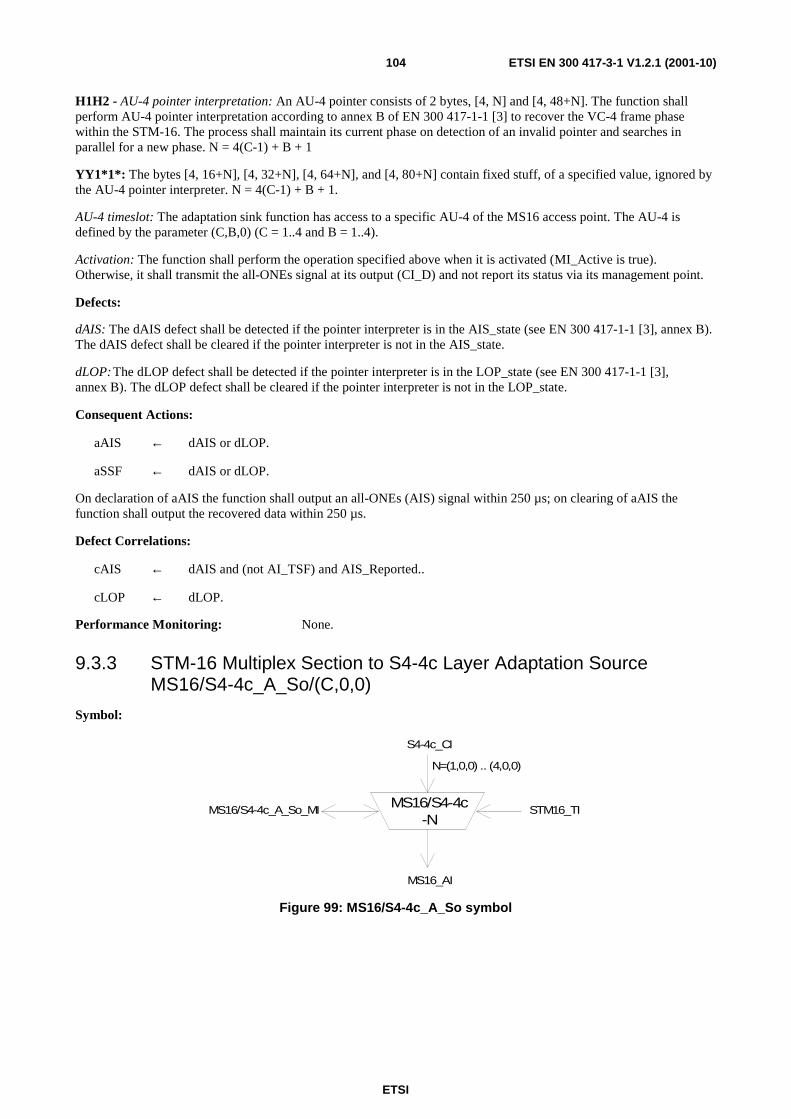
ETSI
ETSI EN 300 417-3-1 V1.2.1 (2001-10)104
H1H2 - AU-4 pointer interpretation: An AU-4 pointer consists of 2 bytes, [4, N] and [4, 48+N]. The function shall perform AU-4 pointer interpretation according to annex B of EN 300 417-1-1 [3] to recover the VC-4 frame phase within the STM-16. The process shall maintain its current phase on detection of an invalid pointer and searches in parallel for a new phase. N = 4(C-1) + B + 1
YY1*1*: The bytes [4, 16+N], [4, 32+N], [4, 64+N], and [4, 80+N] contain fixed stuff, of a specified value, ignored by the AU-4 pointer interpreter. N = 4(C-1) + B + 1.
AU-4 timeslot: The adaptation sink function has access to a specific AU-4 of the MS16 access point. The AU-4 is defined by the parameter (C,B,0) (C = 1..4 and B = 1..4).
Activation: The function shall perform the operation specified above when it is activated (MI_Active is true). Otherwise, it shall transmit the all-ONEs signal at its output (CI_D) and not report its status via its management point.
Defects:
dAIS: The dAIS defect shall be detected if the pointer interpreter is in the AIS_state (see EN 300 417-1-1 [3], annex B). The dAIS defect shall be cleared if the pointer interpreter is not in the AIS_state.
dLOP: The dLOP defect shall be detected if the pointer interpreter is in the LOP_state (see EN 300 417-1-1 [3], annex B). The dLOP defect shall be cleared if the pointer interpreter is not in the LOP_state.
Consequent Actions:
aAIS ← dAIS or dLOP.
aSSF ← dAIS or dLOP.
On declaration of aAIS the function shall output an all-ONEs (AIS) signal within 250 µs; on clearing of aAIS the function shall output the recovered data within 250 µs.
Defect Correlations:
cAIS ← dAIS and (not AI_TSF) and AIS_Reported..
cLOP ← dLOP.
Performance Monitoring: None.
9.3.3 STM-16 Multiplex Section to S4-4c Layer Adaptation Source MS16/S4-4c_A_So/(C,0,0)
Symbol:
MS16/S4-4c-N
S4-4c_CI
MS16_AI
MS16/S4-4c_A_So_MI STM16_TI
N=(1,0,0) .. (4,0,0)
Figure 99: MS16/S4-4c_A_So symbol
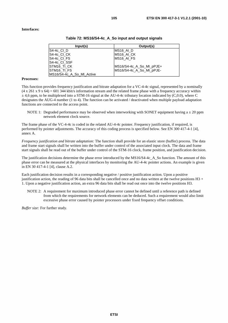
ETSI
ETSI EN 300 417-3-1 V1.2.1 (2001-10)105
Interfaces:
Table 72: MS16/S4-4c_A_So input and output signals
Input(s) Output(s) S4-4c_CI_D S4-4c_CI_CK S4-4c_CI_FS S4-4c_CI_SSF STM16_TI_CK STM16_TI_FS MS16/S4-4c_A_So_MI_Active
MS16_AI_D MS16_AI_CK MS16_AI_FS MS16/S4-4c_A_So_MI_pPJE+ MS16/S4-4c_A_So_MI_pPJE-
Processes:
This function provides frequency justification and bitrate adaptation for a VC-4-4c signal, represented by a nominally (4 x 261 x 9 x 64) = 601 344 kbit/s information stream and the related frame phase with a frequency accuracy within ± 4,6 ppm, to be multiplexed into a STM-16 signal at the AU-4-4c tributary location indicated by (C,0.0), where C designates the AUG-4 number (1 to 4). The function can be activated / deactivated when multiple payload adaptation functions are connected to the access point.
NOTE 1: Degraded performance may be observed when interworking with SONET equipment having a ± 20 ppm network element clock source.
The frame phase of the VC-4-4c is coded in the related AU-4-4c pointer. Frequency justification, if required, is performed by pointer adjustments. The accuracy of this coding process is specified below. See EN 300 417-4-1 [4], annex A.
Frequency justification and bitrate adaptation: The function shall provide for an elastic store (buffer) process. The data and frame start signals shall be written into the buffer under control of the associated input clock. The data and frame start signals shall be read out of the buffer under control of the STM-16 clock, frame position, and justification decision.
The justification decisions determine the phase error introduced by the MS16/S4-4c_A_So function. The amount of this phase error can be measured at the physical interfaces by monitoring the AU-4-4c pointer actions. An example is given in EN 30 417-4-1 [4], clause A.2.
Each justification decision results in a corresponding negative / positive justification action. Upon a positive justification action, the reading of 96 data bits shall be cancelled once and no data written at the twelve positions H3 + 1. Upon a negative justification action, an extra 96 data bits shall be read out once into the twelve positions H3.
NOTE 2: A requirement for maximum introduced phase error cannot be defined until a reference path is defined from which the requirements for network elements can be deduced. Such a requirement would also limit excessive phase error caused by pointer processors under fixed frequency offset conditions.
Buffer size: For further study.
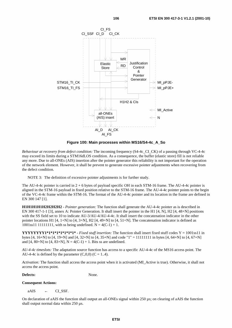
ETSI
ETSI EN 300 417-3-1 V1.2.1 (2001-10)106
ElasticStore
JustificationControl
&Pointer
Generator
STM16_TI_FS
STM16_TI_CK
WR
RD
all-ONEs(AIS) insert
CI_SSF CI_DCI_FS
CI_CK
AI_DAI_FS
AI_CK
H1H2 & CIs
MI_pPJE-
MI_pPJE+
MI_Active
N
Figure 100: Main processes within MS16/S4-4c_A_So
Behaviour at recovery from defect condition: The incoming frequency (S4-4c_CI_CK) of a passing through VC-4-4c may exceed its limits during a STM16dLOS condition. As a consequence, the buffer (elastic store) fill is not reliable any more. Due to all-ONEs (AIS) insertion after the pointer generator this reliability is not important for the operation of the network element. However, it shall be prevent to generate excessive pointer adjustments when recovering from the defect condition.
NOTE 3: The definition of excessive pointer adjustments is for further study.
The AU-4-4c pointer is carried in 2 + 6 bytes of payload specific OH in each STM-16 frame. The AU-4-4c pointer is aligned in the STM-16 payload in fixed position relative to the STM-16 frame. The AU-4-4c pointer points to the begin of the VC-4-4c frame within the STM-16. The format of the AU-4-4c pointer and its location in the frame are defined in EN 300 147 [1].
H1H1H1H1H2H2H2H2 - Pointer generation: The function shall generate the AU-4-4c pointer as is described in EN 300 417-1-1 [3], annex A: Pointer Generation. It shall insert the pointer in the H1 [4, N], H2 [4, 48+N] positions with the SS field set to 10 to indicate AU-3/AU-4/AU-4-4c. It shall insert the concatenation indicator in the other pointer locations H1 [4, 1+N] to [4, 3+N], H2 [4, 49+N] to [4, 51+N]. The concatenation indicator is defined as 1001ss11 11111111, with ss being undefined. N = 4(C-1) + 1.
YYYYYYYY1*1*1*1*1*1*1*1* - Fixed stuff insertion: The function shall insert fixed stuff codes Y = 1001ss11 in bytes [4, 16+N] to [4, 19+N] and [4, 32+N] to [4, 35+N] and code "1" = 11111111 in bytes [4, 64+N] to [4, 67+N] and [4, 80+N] to [4, 83+N], N = 4(C-1) + 1. Bits ss are undefined.
AU-4-4c timeslots: The adaptation source function has access to a specific AU-4-4c of the MS16 access point. The AU-4-4c is defined by the parameter (C,0,0) (C = 1..4).
Activation: The function shall access the access point when it is activated (MI_Active is true). Otherwise, it shall not access the access point.
Defects: None.
Consequent Actions:
aAIS ← CI_SSF.
On declaration of aAIS the function shall output an all-ONEs signal within 250 µs; on clearing of aAIS the function shall output normal data within 250 µs.
ETSI
ETSI EN 300 417-3-1 V1.2.1 (2001-10)107
NOTE 4: If CI_SSF is not connected (when MS16/S4-4c_A_So is connected to a S4-4c_TT_So), CI_SSF is assumed to be false.
Defect Correlations: None.
Performance Monitoring:
Every second the number of generated pointer increments within that second shall be counted as the pPJE+. Every second the number of generated pointer decrements within that second shall be counted as the pPJE-.
NOTE 5: This is applicable for a passing through VC-4-4c only. A locally generated VC-4-4c may have a fixed frame phase; pointer justifications will not occur.
9.3.4 STM-16 Multiplex Section to S4-4c Layer Adaptation Sink MS16/S4-4c_A_Sk/(C,0,0)
Symbol:
MS16/S4-4c-N
S4-4c_CI
MS16_AI
MS16/S4-4c_A_Sk_MI
N=(1,0,0) .. (4,0,0)
Figure 101: MS16/S4-4c_A_Sk symbol
Interfaces:
Table 73: MS16/S4-4c_A_Sk input and output signals
Input(s) Output(s) MS16_AI_D MS16_AI_CK MS16_AI_FS MS16_AI_TSF MS16/S4-4c_A_Sk_MI_Active MS16/S4-4c_A_Sk_MI_AIS_Reported
S4-4c_CI_D S4-4c_CI_CK S4-4c_CI_FS S4-4c_CI_SSF MS16/S4-4c_A_Sk_MI_cAIS MS16/S4-4c_A_Sk_MI_cLOP
Processes:
This function recovers the VC-4-4c data with frame phase information from the STM-16 as defined in EN 300 147 [1]. The VC-4-4c is extracted from tributary location indicated by (C,0.0), where C designates the AUG-4 number (1 to 4). The function can be activated / deactivated when multiple payload adaptation functions are connected to the access point.
H1 H1H1H1H2H2H2H2 - AU-4-4c pointer interpretation: An AU-4-4c pointer consists of 2 bytes, [4, N] and [4, 48 + N]. There will be 3 concatenation indicators, each 2 bytes long, in [4, 1+N]/[4, 49+N], [4, 2+N]/[4, 50+N], and [4, 3 + N]/[4, 51 + N]. The function shall perform AU-4-4c pointer interpretation according to annex B of EN 300 417-1-1 [3] to recover the VC-4-4c frame phase within the STM-16. The process shall maintain its current phase on detection of an invalid pointer and searches in parallel for a new phase. N = 4(C-1) + 1.
YYYYYYYY1*1*1*1*1*1*1*1*: The bytes [4, 16 + N] to [4, 19 + N], [4, 32 + N] to [4, 35 + N], [4, 64 + N] to [4, 67 + N] and [4, 80 + N] to [4, 83 + N] contain fixed stuff, of a specified value, ignored by the AU-4-4c pointer interpreter, N = 4(C-1) + 1.
AU-4-4c timeslots: The adaptation source function has access to a specific AU-4-4c of the MS16 access point. The AU-4-4c is defined by the parameter (C,0,0) (C = 1..4).

ETSI
ETSI EN 300 417-3-1 V1.2.1 (2001-10)108
Activation: The function shall perform the operation specified above when it is activated (MI_Active is true). Otherwise, it shall transmit the all-ONEs signal at its output (CI_D) and not report its status via its management point.
Defects:
dAIS: The dAIS defect shall be detected if the pointer interpreter is in the AISX_state (see EN 300 417-1-1 [3], annex B). The dAIS defect shall be cleared if the pointer interpreter is not in the AISX_state.
dLOP: The dLOP defect shall be detected if the pointer interpreter is in the LOPX_state (see EN 300 417-1-1 [3], annex B). The dLOP defect shall be cleared if the pointer interpreter is not in the LOPX_state.
Consequent Actions:
aAIS ← dAIS or dLOP.
aSSF ← dAIS or dLOP.
On declaration of aAIS the function shall output an all-ONEs (AIS) signal within 250 µs; on clearing of aAIS the function shall output the recovered data within 250 µs.
Defect Correlations:
cAIS ← dAIS and (not aTSF) and AIS_Reported.
cLOP ← dLOP.
Performance Monitoring: None.
9.3.5 STM-16 Multiplex Section to S4-16c Layer Adaptation Source MS16/S4-16c_A_So
Symbol:
MS16/S4-16c
S4-16c_CI
M S16_AI
S16/S4-16c_A_So_M I STM 16_TI
Figure 102: MS16/S4-16c_A_So symbol
Interfaces:
Table 74: MS16/S4-16c_A_So input and output signals
Input(s) Output(s) S4-16c_CI_D S4-16c_CI_CK S4-16c_CI_FS S4-16c_CI_SSF STM16_TI_CK STM16_TI_FS MS16/S4-16c_A_So_MI_Active
MS16_AI_D MS16_AI_CK MS16_AI_FS MS16/S4-16c_A_So_MI_pPJE+ MS16/S4-16c_A_So_MI_pPJE-

ETSI
ETSI EN 300 417-3-1 V1.2.1 (2001-10)109
Processes:
This function provides frequency justification and bitrate adaptation for a VC-4-16c signal, represented by a nominally (16 x 261 x 9 x 64) = 2 405 376 kbit/s information stream and the related frame phase with a frequency accuracy within ± 4,6 ppm, to be multiplexed into a STM-16 signal at the AU-4-16c tributary location. The function can be activated / deactivated when multiple payload adaptation functions are connected to the access point.
NOTE 1: Degraded performance may be observed when interworking with SONET equipment having a ± 20 ppm network element clock source.
The frame phase of the VC-4-16c is coded in the related AU-4-16c pointer. Frequency justification, if required, is performed by pointer adjustments. The accuracy of this coding process is specified below. See EN 300 417-4-1 [4], annex A.
Frequency justification and bitrate adaptation: The function shall provide for an elastic store (buffer) process. The data and frame start signals shall be written into the buffer under control of the associated input clock. The data and frame start signals shall be read out of the buffer under control of the STM-16 clock, frame position, and justification decision.
The justification decisions determine the phase error introduced by the MS16/S4-16c_A_So function. The amount of this phase error can be measured at the physical interfaces by monitoring the AU-4-16c pointer actions. An example is given in EN 30 417-4-1 [4], clause A.2.
Each justification decision results in a corresponding negative / positive justification action. Upon a positive justification action, the reading of 96 data bits shall be cancelled once and no data written at the 48 positions H3 + 1. Upon a negative justification action, an extra 384 data bits shall be read out once into the 48 positions H3.
NOTE 2: A requirement for maximum introduced phase error cannot be defined until a reference path is defined from which the requirements for network elements can be deduced. Such a requirement would also limit excessive phase error caused by pointer processors under fixed frequency offset conditions.
Buffer size: For further study.
ElasticStore
JustificationControl
&Pointer
Generator
STM16_TI_FS
STM16_TI_CK
WR
RD
all-ONEs(AIS) insert
CI_SSF CI_DCI_FS
CI_CK
AI_DAI_FS
AI_CK
H1H2 & CIs
MI_pPJE-
MI_pPJE+
MI_Active
N
Figure 103: Main processes within MS16/S4-16c_A_So
ETSI
ETSI EN 300 417-3-1 V1.2.1 (2001-10)110
Behaviour at recovery from defect condition: The incoming frequency (S4-16c_CI_CK) of a passing through VC-4-16c may exceed its limits during a STM16dLOS condition. As a consequence, the buffer (elastic store) fill is not reliable any more. Due to all-ONEs (AIS) insertion after the pointer generator this reliability is not important for the operation of the network element. However, it shall be prevent to generate excessive pointer adjustments when recovering from the defect condition.
NOTE 3: The definition of excessive pointer adjustments is for further study.
The AU-4-16c pointer is carried in 2 + 30 bytes of payload specific OH in each STM-16 frame. The AU-4-16c pointer is aligned in the STM-16 payload in fixed position relative to the STM-16 frame. The AU-4-16c pointer points to the begin of the VC-4-16c frame within the STM-16. The format of the AU-4-16c pointer and its location in the frame are defined in EN 300 147 [1].
H116H216 - Pointer generation: The function shall generate the AU-4-16c pointer as is described in EN 300 417-1-1 [3], annex A: Pointer Generation. It shall insert the pointer in the H1 [4, 1], H2 [4, 49] positions with the SS field set to 10 to indicate AU-3/AU-4/ AU-4-4c /AU-4-16c. It shall insert the concatenation indicator in the other pointer locations H1 [4, 2] to [4, 48], H2 [4, 50] to [4, 96]. The concatenation indicator is defined as 1001ss11 11111111, with ss being undefined.
Y321*32 - Fixed stuff insertion: The function shall insert fixed stuff codes Y = 1001ss11 in bytes [4, 17] to [4, 48] and code "1" = 11111111 in bytes [4, 65] to [4, 96]. Bits ss are undefined.
Activation: The function shall access the access point when it is activated (MI_Active is true). Otherwise, it shall not access the access point.
Defects: None.
Consequent Actions:
aAIS ← CI_SSF.
On declaration of aAIS the function shall output an all-ONEs signal within 250 µs; on clearing of aAIS the function shall output normal data within 250 µs.
NOTE 4: If CI_SSF is not connected (when MS16/S4-16c_A_So is connected to a S4-16c_TT_So), CI_SSF is assumed to be false.
Defect Correlations: None.
Performance Monitoring:
Every second the number of generated pointer increments within that second shall be counted as the pPJE+. Every second the number of generated pointer decrements within that second shall be counted as the pPJE-.
NOTE 5: This is applicable for a passing through VC-4-16c only. A locally generated VC-4-16c may have a fixed frame phase; pointer justifications will not occur.
9.3.6 STM-16 Multiplex Section to S4-16c Layer Adaptation Sink MS16/S4-16c_A_Sk
Symbol:
MS16/S4-16c
S4-16c_CI
M S16_AI
M S16/S4-16c_A_Sk_M I
Figure 104: MS16/S4-16c_A_Sk symbol
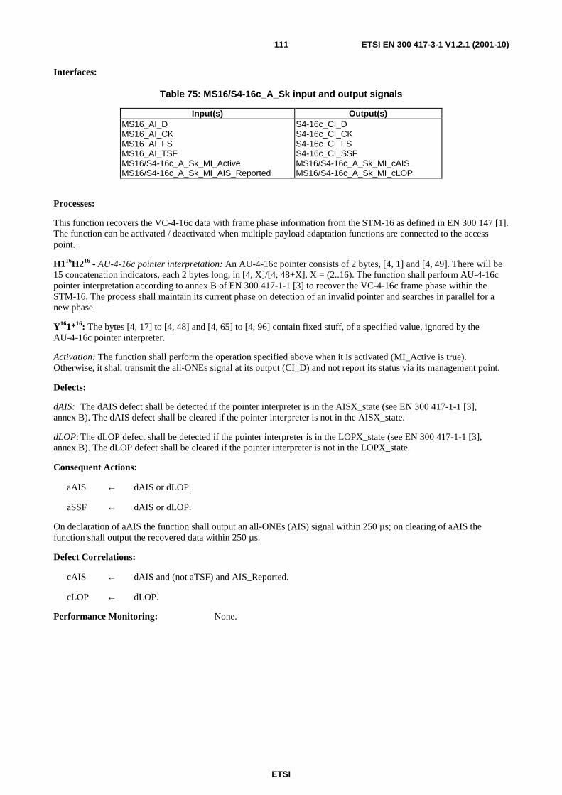
ETSI
ETSI EN 300 417-3-1 V1.2.1 (2001-10)111
Interfaces:
Table 75: MS16/S4-16c_A_Sk input and output signals
Input(s) Output(s) MS16_AI_D MS16_AI_CK MS16_AI_FS MS16_AI_TSF MS16/S4-16c_A_Sk_MI_Active MS16/S4-16c_A_Sk_MI_AIS_Reported
S4-16c_CI_D S4-16c_CI_CK S4-16c_CI_FS S4-16c_CI_SSF MS16/S4-16c_A_Sk_MI_cAIS MS16/S4-16c_A_Sk_MI_cLOP
Processes:
This function recovers the VC-4-16c data with frame phase information from the STM-16 as defined in EN 300 147 [1]. The function can be activated / deactivated when multiple payload adaptation functions are connected to the access point.
H116H216 - AU-4-16c pointer interpretation: An AU-4-16c pointer consists of 2 bytes, [4, 1] and [4, 49]. There will be 15 concatenation indicators, each 2 bytes long, in [4, X]/[4, 48+X], X = (2..16). The function shall perform AU-4-16c pointer interpretation according to annex B of EN 300 417-1-1 [3] to recover the VC-4-16c frame phase within the STM-16. The process shall maintain its current phase on detection of an invalid pointer and searches in parallel for a new phase.
Y161*16: The bytes [4, 17] to [4, 48] and [4, 65] to [4, 96] contain fixed stuff, of a specified value, ignored by the AU-4-16c pointer interpreter.
Activation: The function shall perform the operation specified above when it is activated (MI_Active is true). Otherwise, it shall transmit the all-ONEs signal at its output (CI_D) and not report its status via its management point.
Defects:
dAIS: The dAIS defect shall be detected if the pointer interpreter is in the AISX_state (see EN 300 417-1-1 [3], annex B). The dAIS defect shall be cleared if the pointer interpreter is not in the AISX_state.
dLOP: The dLOP defect shall be detected if the pointer interpreter is in the LOPX_state (see EN 300 417-1-1 [3], annex B). The dLOP defect shall be cleared if the pointer interpreter is not in the LOPX_state.
Consequent Actions:
aAIS ← dAIS or dLOP.
aSSF ← dAIS or dLOP.
On declaration of aAIS the function shall output an all-ONEs (AIS) signal within 250 µs; on clearing of aAIS the function shall output the recovered data within 250 µs.
Defect Correlations:
cAIS ← dAIS and (not aTSF) and AIS_Reported.
cLOP ← dLOP.
Performance Monitoring: None.

ETSI
ETSI EN 300 417-3-1 V1.2.1 (2001-10)112
9.3.7 STM-16 Multiplex Section to DCC Adaptation Source MS16/DCC_A_So
Symbol:
MS16/DCC
DCC_CI_D
MS16_AI
STM16_TI
DCC_CI_CK
Figure 105: MS16/DCC_A_So symbol
Interfaces:
Table 76: MS16/DCC_A_So input and output signals
Input(s) Output(s) DCC_CI_D STM16_TI_CK STM16_TI_FS
MS16_AI_D DCC_CI_CK
Processes:
The function multiplexes the DCC CI data (576 kbit/s) into the byte locations D4 to D12 as defined in EN 300 147 [1] and depicted in figure 90.
NOTE: DCC transmission can be "disabled" when the matrix connection in the connected DCC_C function is removed.
Defects: None.
Consequent Actions: None.
Defect Correlations: None.
Performance Monitoring: None.
9.3.8 STM-16 Multiplex Section to DCC Adaptation Sink MS16/DCC_A_Sk
Symbol:
MS16/DCC
DCC_CI
MS16_AI
Figure 106: MS16/DCC_A_Sk symbol

ETSI
ETSI EN 300 417-3-1 V1.2.1 (2001-10)113
Interfaces:
Table 77: MS16/DCC_A_Sk input and output signals
Input(s) Output(s) MS16_AI_D MS16_AI_CK MS16_AI_FS MS16_AI_TSF
DCC_CI_D DCC_CI_CK DCC_CI_SSF
Processes:
The function separates DCC data from MS Overhead as defined in EN 300 147 [1] and depicted in figure 90.
NOTE: DCC processing can be "disabled" when the matrix connection in the connected DCC_C function is removed.
Defects: None.
Consequent Actions:
aSSF ← AI_TSF.
Defect Correlations: None.
Performance Monitoring: None.
9.3.9 STM-16 Multiplex Section to P0s Adaptation Source MS16/P0s_A_So
Symbol:
MS16/P0s
P0s_CI
MS16_AI
STM16_TI
Figure 107: MS16/P0s_A_So symbol
Interfaces:
Table 78: MS16/P0s_A_So input and output signals
Input(s) Output(s) P0s_CI_D P0s_CI_CK P0s_CI_FS STM16_TI_CK STM16_TI_FS
MS16/P0s_AI_So_D
Processes:
This function provides the multiplexing of a 64 kbit/s orderwire information stream into the MS16_AI using slip buffering. It takes P0s_CI, defined in EN 300 166 [2] as an octet structured bit-stream with a synchronous bit rate of 64 kbit/s , present at its input and inserts it into the MSOH byte E2 as defined in EN 300 147 [1] and depicted in figure 90.
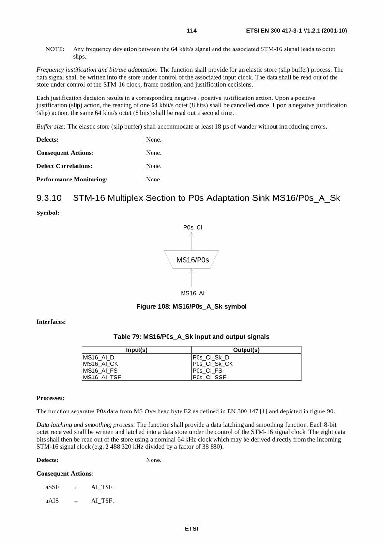
ETSI
ETSI EN 300 417-3-1 V1.2.1 (2001-10)114
NOTE: Any frequency deviation between the 64 kbit/s signal and the associated STM-16 signal leads to octet slips.
Frequency justification and bitrate adaptation: The function shall provide for an elastic store (slip buffer) process. The data signal shall be written into the store under control of the associated input clock. The data shall be read out of the store under control of the STM-16 clock, frame position, and justification decisions.
Each justification decision results in a corresponding negative / positive justification action. Upon a positive justification (slip) action, the reading of one 64 kbit/s octet (8 bits) shall be cancelled once. Upon a negative justification (slip) action, the same 64 kbit/s octet (8 bits) shall be read out a second time.
Buffer size: The elastic store (slip buffer) shall accommodate at least 18 µs of wander without introducing errors.
Defects: None.
Consequent Actions: None.
Defect Correlations: None.
Performance Monitoring: None.
9.3.10 STM-16 Multiplex Section to P0s Adaptation Sink MS16/P0s_A_Sk
Symbol:
MS16/P0s
P0s_CI
MS16_AI
Figure 108: MS16/P0s_A_Sk symbol
Interfaces:
Table 79: MS16/P0s_A_Sk input and output signals
Input(s) Output(s) MS16_AI_D MS16_AI_CK MS16_AI_FS MS16_AI_TSF
P0s_CI_Sk_D P0s_CI_Sk_CK P0s_CI_FS P0s_CI_SSF
Processes:
The function separates P0s data from MS Overhead byte E2 as defined in EN 300 147 [1] and depicted in figure 90.
Data latching and smoothing process: The function shall provide a data latching and smoothing function. Each 8-bit octet received shall be written and latched into a data store under the control of the STM-16 signal clock. The eight data bits shall then be read out of the store using a nominal 64 kHz clock which may be derived directly from the incoming STM-16 signal clock (e.g. 2 488 320 kHz divided by a factor of 38 880).
Defects: None.
Consequent Actions:
aSSF ← AI_TSF.
aAIS ← AI_TSF.
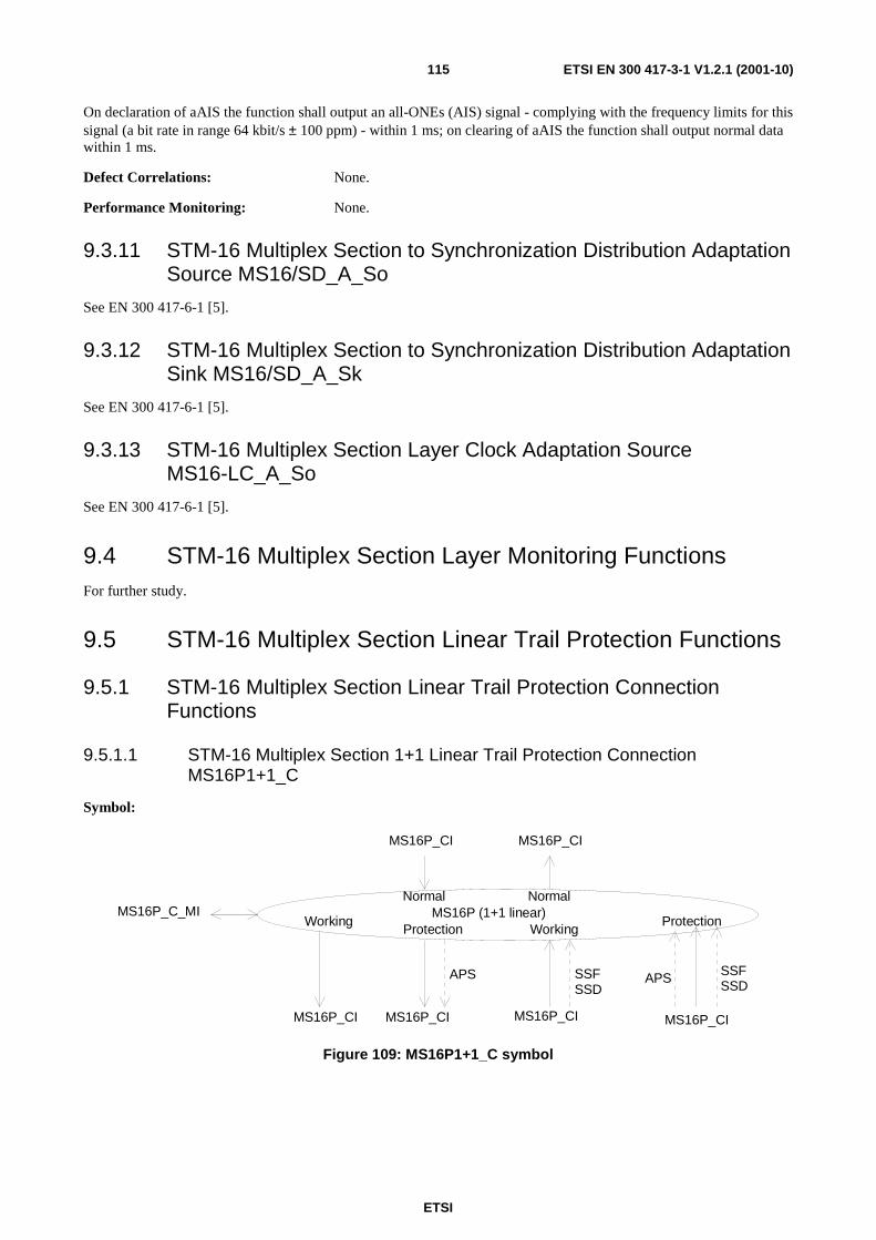
ETSI
ETSI EN 300 417-3-1 V1.2.1 (2001-10)115
On declaration of aAIS the function shall output an all-ONEs (AIS) signal - complying with the frequency limits for this signal (a bit rate in range 64 kbit/s ± 100 ppm) - within 1 ms; on clearing of aAIS the function shall output normal data within 1 ms.
Defect Correlations: None.
Performance Monitoring: None.
9.3.11 STM-16 Multiplex Section to Synchronization Distribution Adaptation Source MS16/SD_A_So
See EN 300 417-6-1 [5].
9.3.12 STM-16 Multiplex Section to Synchronization Distribution Adaptation Sink MS16/SD_A_Sk
See EN 300 417-6-1 [5].
9.3.13 STM-16 Multiplex Section Layer Clock Adaptation Source MS16-LC_A_So
See EN 300 417-6-1 [5].
9.4 STM-16 Multiplex Section Layer Monitoring Functions For further study.
9.5 STM-16 Multiplex Section Linear Trail Protection Functions
9.5.1 STM-16 Multiplex Section Linear Trail Protection Connection Functions
9.5.1.1 STM-16 Multiplex Section 1+1 Linear Trail Protection Connection MS16P1+1_C
Symbol:
MS16P_CI MS16P_CI
MS16P (1+1 linear)
APS SSFSSD
WorkingProtection Working
APS SSFSSD
Protection
MS16P_CI MS16P_CI
MS16P_CI MS16P_CI
Normal NormalMS16P_C_MI
Figure 109: MS16P1+1_C symbol

ETSI
ETSI EN 300 417-3-1 V1.2.1 (2001-10)116
Interfaces:
Table 80: MS16P1+1_C input and output signals
Input(s) Output(s) For connection points W and P: MS16P_CI_D MS16P_CI_CK MS16P_CI_FS MS16P_CI_SSF MS16P_CI_SSD For connection points N: MS16P_CI_D MS16P_CI_CK MS16P_CI_FS Per function: MS16P_CI_APS MS16P_C_MI_SWtype MS16P_C_MI_OPERtype MS16P_C_MI_WTRTime MS16P_C_MI_EXTCMD
For connection points W and P: MS16P_CI_D MS16P_CI_CK MS16P_CI_FS MS16P_CI_SSF For connection points N: MS16P_CI_D MS16P_CI_CK MS16P_CI_FS MS16P_CI_SSF Per function: MS16P_CI_APS MS16P_C_MI_cFOP
NOTE: Protection status reporting signals are for further study.
Processes:
The function performs the STM-16 linear multiplex section protection process for 1 + 1 protection architectures; see EN 300 417-1-1 [3], clause 9.2. It performs the bridge and selector functionality as presented in figure 48 of EN 300 417-1-1 [3]. In the sink direction, the signal output at the normal #1 reference point can be the signal received via either the associated working #1 section or the protection section; this is determined by the SF, SD conditions (relayed via CI_SSF, CI_SSD signals), the external commands and the information relayed via the APS signal. In the source direction, the working outputs are connected to the associated normal inputs. The protection output is outsourced (no input connected) or connected to any normal input.
Provided no protection switching action is activated / required the following changes to (the configuration of) a connection shall be possible without disturbing the CI passing the connection:
- change between switching types;
- change between operation types;
- change of WTR time.
MS Protection Operation: The MS trail protection process shall operate as specified in annex A, according the following characteristics.
Table 81: "Parameters for MS16P1+1_C protection process"
Architecture: 1 + 1 Switching type: uni-directional or bi-directional Operation type: revertive or non-revertive APS channel: 13 bits, K1[1-8] and K2[1-5] Wait-To-Restore time: in the order of 0-12 minutes Switching time: ≤ 50 ms Hold-off time: not applicable Signal switch conditions: SF, SD External commands: (revertive operation) LO, FSw-#1, MSw-#1, CLR, EXER-#1
(non-revertive operation) LO or FSw, FSw-#i, MSw, MSw-#i, CLR, EXER-#1
SFpriority, SDpriority: high
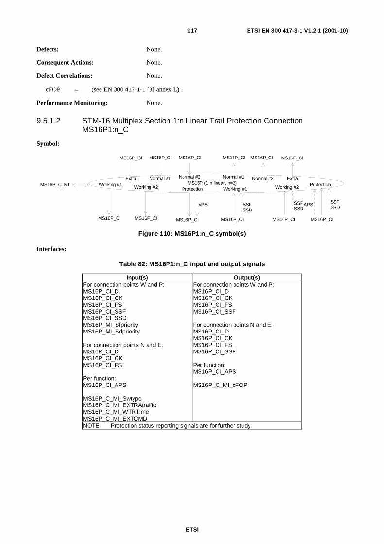
ETSI
ETSI EN 300 417-3-1 V1.2.1 (2001-10)117
Defects: None.
Consequent Actions: None.
Defect Correlations: None.
cFOP ← (see EN 300 417-1-1 [3] annex L).
Performance Monitoring: None.
9.5.1.2 STM-16 Multiplex Section 1:n Linear Trail Protection Connection MS16P1:n_C
Symbol:
MS16P_CI MS16P_CI
MS16P (1:n linear, n=2)
APS SSFSSD
Working #1Protection Working #1
MS16P_CI
Working #2
SSFSSD
Working #2
APS SSFSSD
Protection
MS16P_CI MS16P_CI MS16P_CI
MS16P_CI MS16P_CI MS16P_CI MS16P_CI
MS16P_C_MINormal #1 Normal #2Normal #1Normal #2
MS16P_CI
Extra
MS16P_CI
Extra
Figure 110: MS16P1:n_C symbol(s)
Interfaces:
Table 82: MS16P1:n_C input and output signals
Input(s) Output(s) For connection points W and P: MS16P_CI_D MS16P_CI_CK MS16P_CI_FS MS16P_CI_SSF MS16P_CI_SSD MS16P_MI_Sfpriority MS16P_MI_Sdpriority For connection points N and E: MS16P_CI_D MS16P_CI_CK MS16P_CI_FS Per function: MS16P_CI_APS MS16P_C_MI_Swtype MS16P_C_MI_EXTRAtraffic MS16P_C_MI_WTRTime MS16P_C_MI_EXTCMD
For connection points W and P: MS16P_CI_D MS16P_CI_CK MS16P_CI_FS MS16P_CI_SSF For connection points N and E: MS16P_CI_D MS16P_CI_CK MS16P_CI_FS MS16P_CI_SSF Per function: MS16P_CI_APS MS16P_C_MI_cFOP
NOTE: Protection status reporting signals are for further study.
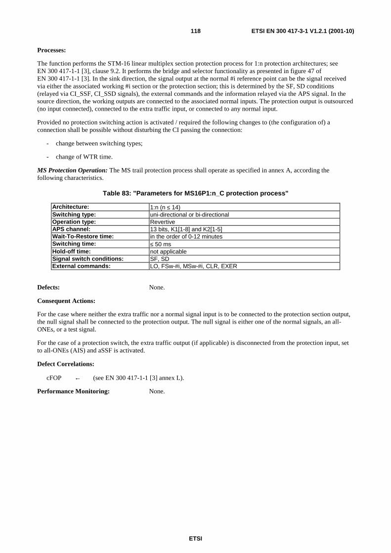
ETSI
ETSI EN 300 417-3-1 V1.2.1 (2001-10)118
Processes:
The function performs the STM-16 linear multiplex section protection process for 1:n protection architectures; see EN 300 417-1-1 [3], clause 9.2. It performs the bridge and selector functionality as presented in figure 47 of EN 300 417-1-1 [3]. In the sink direction, the signal output at the normal #i reference point can be the signal received via either the associated working #i section or the protection section; this is determined by the SF, SD conditions (relayed via CI_SSF, CI_SSD signals), the external commands and the information relayed via the APS signal. In the source direction, the working outputs are connected to the associated normal inputs. The protection output is outsourced (no input connected), connected to the extra traffic input, or connected to any normal input.
Provided no protection switching action is activated / required the following changes to (the configuration of) a connection shall be possible without disturbing the CI passing the connection:
- change between switching types;
- change of WTR time.
MS Protection Operation: The MS trail protection process shall operate as specified in annex A, according the following characteristics.
Table 83: "Parameters for MS16P1:n_C protection process"
Architecture: 1:n (n ≤ 14) Switching type: uni-directional or bi-directional Operation type: Revertive APS channel: 13 bits, K1[1-8] and K2[1-5] Wait-To-Restore time: in the order of 0-12 minutes Switching time: ≤ 50 ms Hold-off time: not applicable Signal switch conditions: SF, SD External commands: LO, FSw-#i, MSw-#i, CLR, EXER
Defects: None.
Consequent Actions:
For the case where neither the extra traffic nor a normal signal input is to be connected to the protection section output, the null signal shall be connected to the protection output. The null signal is either one of the normal signals, an all-ONEs, or a test signal.
For the case of a protection switch, the extra traffic output (if applicable) is disconnected from the protection input, set to all-ONEs (AIS) and aSSF is activated.
Defect Correlations:
cFOP ← (see EN 300 417-1-1 [3] annex L).
Performance Monitoring: None.
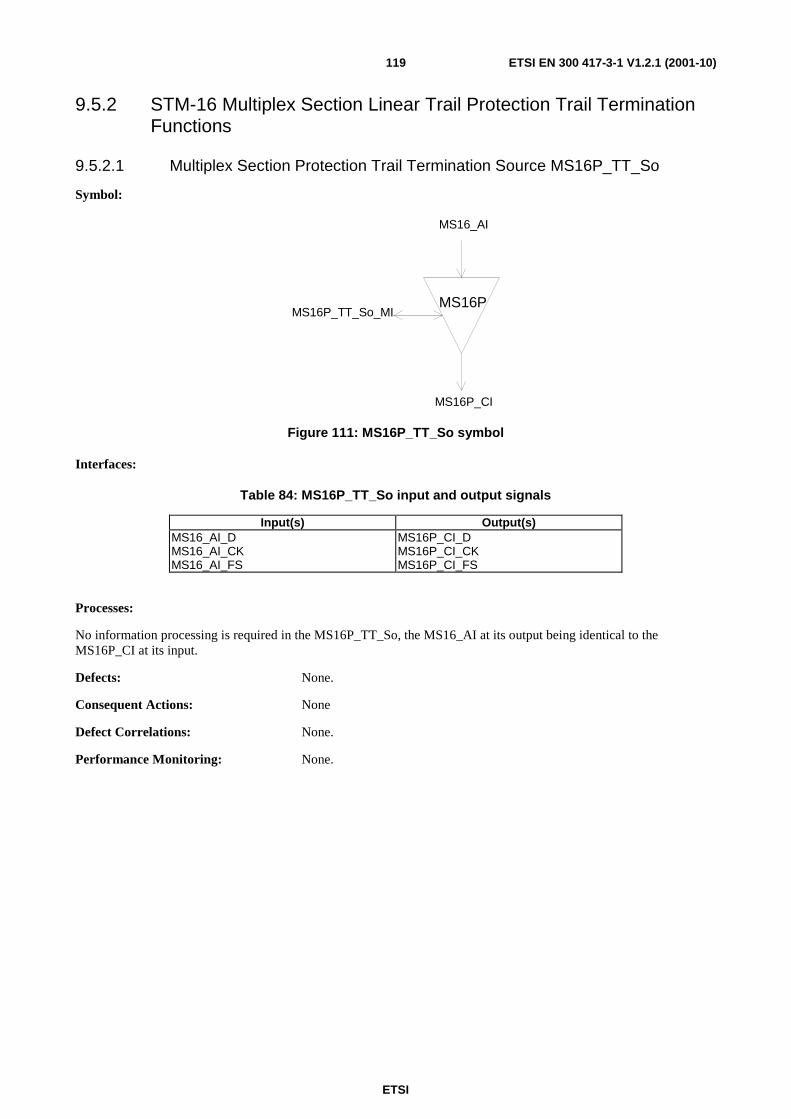
ETSI
ETSI EN 300 417-3-1 V1.2.1 (2001-10)119
9.5.2 STM-16 Multiplex Section Linear Trail Protection Trail Termination Functions
9.5.2.1 Multiplex Section Protection Trail Termination Source MS16P_TT_So
Symbol:
MS16P
MS16_AI
MS16P_CI
MS16P_TT_So_MI
Figure 111: MS16P_TT_So symbol
Interfaces:
Table 84: MS16P_TT_So input and output signals
Input(s) Output(s) MS16_AI_D MS16_AI_CK MS16_AI_FS
MS16P_CI_D MS16P_CI_CK MS16P_CI_FS
Processes:
No information processing is required in the MS16P_TT_So, the MS16_AI at its output being identical to the MS16P_CI at its input.
Defects: None.
Consequent Actions: None
Defect Correlations: None.
Performance Monitoring: None.
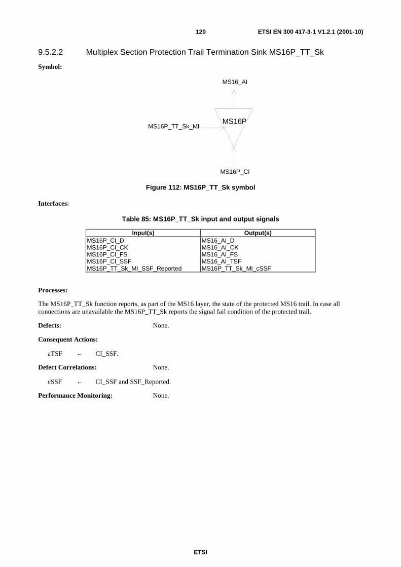
ETSI
ETSI EN 300 417-3-1 V1.2.1 (2001-10)120
9.5.2.2 Multiplex Section Protection Trail Termination Sink MS16P_TT_Sk
Symbol:
MS16P
MS16_AI
MS16P_CI
MS16P_TT_Sk_MI
Figure 112: MS16P_TT_Sk symbol
Interfaces:
Table 85: MS16P_TT_Sk input and output signals
Input(s) Output(s) MS16P_CI_D MS16P_CI_CK MS16P_CI_FS MS16P_CI_SSF MS16P_TT_Sk_MI_SSF_Reported
MS16_AI_D MS16_AI_CK MS16_AI_FS MS16_AI_TSF MS16P_TT_Sk_MI_cSSF
Processes:
The MS16P_TT_Sk function reports, as part of the MS16 layer, the state of the protected MS16 trail. In case all connections are unavailable the MS16P_TT_Sk reports the signal fail condition of the protected trail.
Defects: None.
Consequent Actions:
aTSF ← CI_SSF.
Defect Correlations: None.
cSSF ← CI_SSF and SSF_Reported.
Performance Monitoring: None.
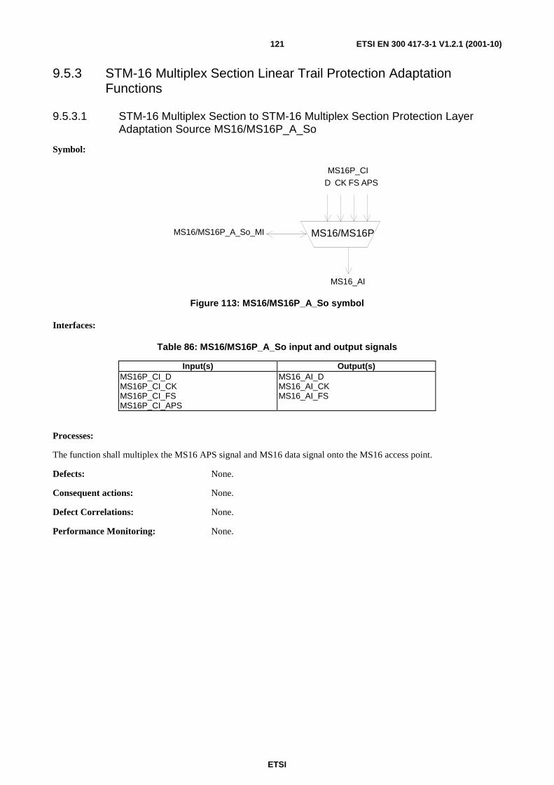
ETSI
ETSI EN 300 417-3-1 V1.2.1 (2001-10)121
9.5.3 STM-16 Multiplex Section Linear Trail Protection Adaptation Functions
9.5.3.1 STM-16 Multiplex Section to STM-16 Multiplex Section Protection Layer Adaptation Source MS16/MS16P_A_So
Symbol:
MS16/MS16P
MS16P_CI
MS16_AI
MS16/MS16P_A_So_MI
D CK FS APS
Figure 113: MS16/MS16P_A_So symbol
Interfaces:
Table 86: MS16/MS16P_A_So input and output signals
Input(s) Output(s) MS16P_CI_D MS16P_CI_CK MS16P_CI_FS MS16P_CI_APS
MS16_AI_D MS16_AI_CK MS16_AI_FS
Processes:
The function shall multiplex the MS16 APS signal and MS16 data signal onto the MS16 access point.
Defects: None.
Consequent actions: None.
Defect Correlations: None.
Performance Monitoring: None.
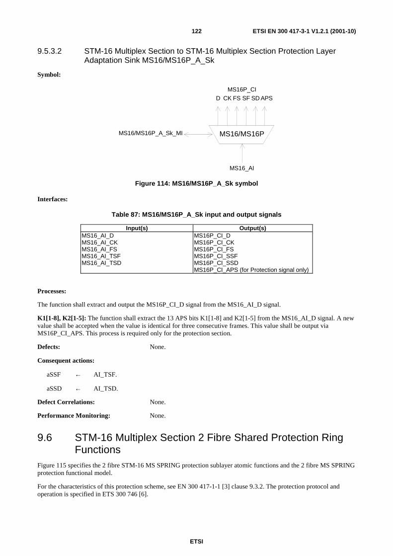
ETSI
ETSI EN 300 417-3-1 V1.2.1 (2001-10)122
9.5.3.2 STM-16 Multiplex Section to STM-16 Multiplex Section Protection Layer Adaptation Sink MS16/MS16P_A_Sk
Symbol:
MS16/MS16P
MS16P_CI
MS16_AI
MS16/MS16P_A_Sk_MI
D CK FS SF SD APS
Figure 114: MS16/MS16P_A_Sk symbol
Interfaces:
Table 87: MS16/MS16P_A_Sk input and output signals
Input(s) Output(s) MS16_AI_D MS16_AI_CK MS16_AI_FS MS16_AI_TSF MS16_AI_TSD
MS16P_CI_D MS16P_CI_CK MS16P_CI_FS MS16P_CI_SSF MS16P_CI_SSD MS16P_CI_APS (for Protection signal only)
Processes:
The function shall extract and output the MS16P_CI_D signal from the MS16_AI_D signal.
K1[1-8], K2[1-5]: The function shall extract the 13 APS bits K1[1-8] and K2[1-5] from the MS16_AI_D signal. A new value shall be accepted when the value is identical for three consecutive frames. This value shall be output via MS16P_CI_APS. This process is required only for the protection section.
Defects: None.
Consequent actions:
aSSF ← AI_TSF.
aSSD ← AI_TSD.
Defect Correlations: None.
Performance Monitoring: None.
9.6 STM-16 Multiplex Section 2 Fibre Shared Protection Ring Functions
Figure 115 specifies the 2 fibre STM-16 MS SPRING protection sublayer atomic functions and the 2 fibre MS SPRING protection functional model.
For the characteristics of this protection scheme, see EN 300 417-1-1 [3] clause 9.3.2. The protection protocol and operation is specified in ETS 300 746 [6].
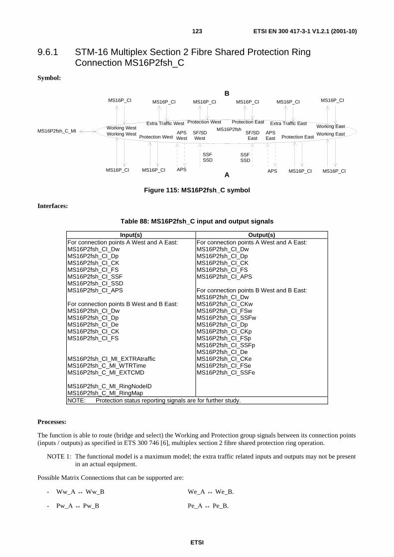
ETSI
ETSI EN 300 417-3-1 V1.2.1 (2001-10)123
9.6.1 STM-16 Multiplex Section 2 Fibre Shared Protection Ring Connection MS16P2fsh_C
Symbol:
MS16P_CI MS16P_CI
MS16P2fsh
APS
SSFSSD
Working West
APS
SSFSSD
Protection West
MS16P_CI
MS16P_CI MS16P_CI
MS16P2fsh_C_MIWorking West
Extra Traffic West
Protection West
MS16P_CI
Working East
Protection East
MS16P_CI
MS16P_CIMS16P_CI
Working EastExtra Traffic East
Protection East
MS16P_CI
APSWest
SF/SDWest
SF/SDEast
APSEast
A
B
Figure 115: MS16P2fsh_C symbol
Interfaces:
Table 88: MS16P2fsh_C input and output signals
Input(s) Output(s) For connection points A West and A East: MS16P2fsh_CI_Dw MS16P2fsh_CI_Dp MS16P2fsh_CI_CK MS16P2fsh_CI_FS MS16P2fsh_CI_SSF MS16P2fsh_CI_SSD MS16P2fsh_CI_APS For connection points B West and B East: MS16P2fsh_CI_Dw MS16P2fsh_CI_Dp MS16P2fsh_CI_De MS16P2fsh_CI_CK MS16P2fsh_CI_FS MS16P2fsh_CI_MI_EXTRAtraffic MS16P2fsh_C_MI_WTRTime MS16P2fsh_C_MI_EXTCMD MS16P2fsh_C_MI_RingNodeID MS16P2fsh_C_MI_RingMap
For connection points A West and A East: MS16P2fsh_CI_Dw MS16P2fsh_CI_Dp MS16P2fsh_CI_CK MS16P2fsh_CI_FS MS16P2fsh_CI_APS For connection points B West and B East: MS16P2fsh_CI_Dw MS16P2fsh_CI_CKw MS16P2fsh_CI_FSw MS16P2fsh_CI_SSFw MS16P2fsh_CI_Dp MS16P2fsh_CI_CKp MS16P2fsh_CI_FSp MS16P2fsh_CI_SSFp MS16P2fsh_CI_De MS16P2fsh_CI_CKe MS16P2fsh_CI_FSe MS16P2fsh_CI_SSFe
NOTE: Protection status reporting signals are for further study.
Processes:
The function is able to route (bridge and select) the Working and Protection group signals between its connection points (inputs / outputs) as specified in ETS 300 746 [6], multiplex section 2 fibre shared protection ring operation.
NOTE 1: The functional model is a maximum model; the extra traffic related inputs and outputs may not be present in an actual equipment.
Possible Matrix Connections that can be supported are:
- Ww_A ↔ Ww_B We_A ↔ We_B.
- Pw_A ↔ Pw_B Pe_A ↔ Pe_B.
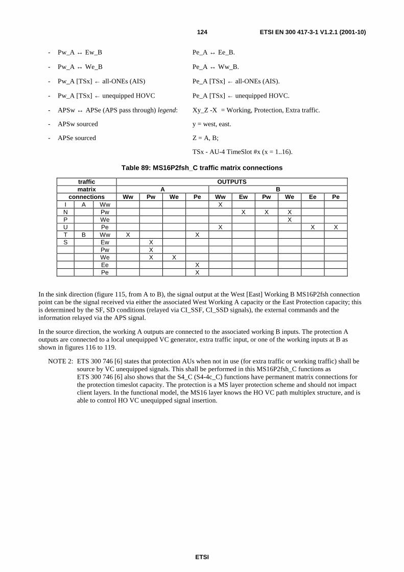
ETSI
ETSI EN 300 417-3-1 V1.2.1 (2001-10)124
- Pw_A ↔ Ew_B Pe_A ↔ Ee_B.
- Pw_A ↔ We_B Pe_A ↔ Ww_B.
- Pw_A [TSx] ← all-ONEs (AIS) Pe_A [TSx] ← all-ONEs (AIS).
- Pw_A [TSx] ← unequipped HOVC Pe_A [TSx] ← unequipped HOVC.
- APSw ↔ APSe (APS pass through) legend: Xy_Z -X = Working, Protection, Extra traffic.
- APSw sourced y = west, east.
- APSe sourced Z = A, B;
TSx - AU-4 TimeSlot #x (x = 1..16).
Table 89: MS16P2fsh_C traffic matrix connections
traffic OUTPUTS matrix A B
connections Ww Pw We Pe Ww Ew Pw We Ee Pe I A Ww X N Pw X X X P We X U Pe X X X T B Ww X X S Ew X Pw X We X X Ee X Pe X
In the sink direction (figure 115, from A to B), the signal output at the West [East] Working B MS16P2fsh connection point can be the signal received via either the associated West Working A capacity or the East Protection capacity; this is determined by the SF, SD conditions (relayed via CI_SSF, CI_SSD signals), the external commands and the information relayed via the APS signal.
In the source direction, the working A outputs are connected to the associated working B inputs. The protection A outputs are connected to a local unequipped VC generator, extra traffic input, or one of the working inputs at B as shown in figures 116 to 119.
NOTE 2: ETS 300 746 [6] states that protection AUs when not in use (for extra traffic or working traffic) shall be source by VC unequipped signals. This shall be performed in this MS16P2fsh_C functions as ETS 300 746 [6] also shows that the S4_C (S4-4c_C) functions have permanent matrix connections for the protection timeslot capacity. The protection is a MS layer protection scheme and should not impact client layers. In the functional model, the MS16 layer knows the HO VC path multiplex structure, and is able to control HO VC unequipped signal insertion.
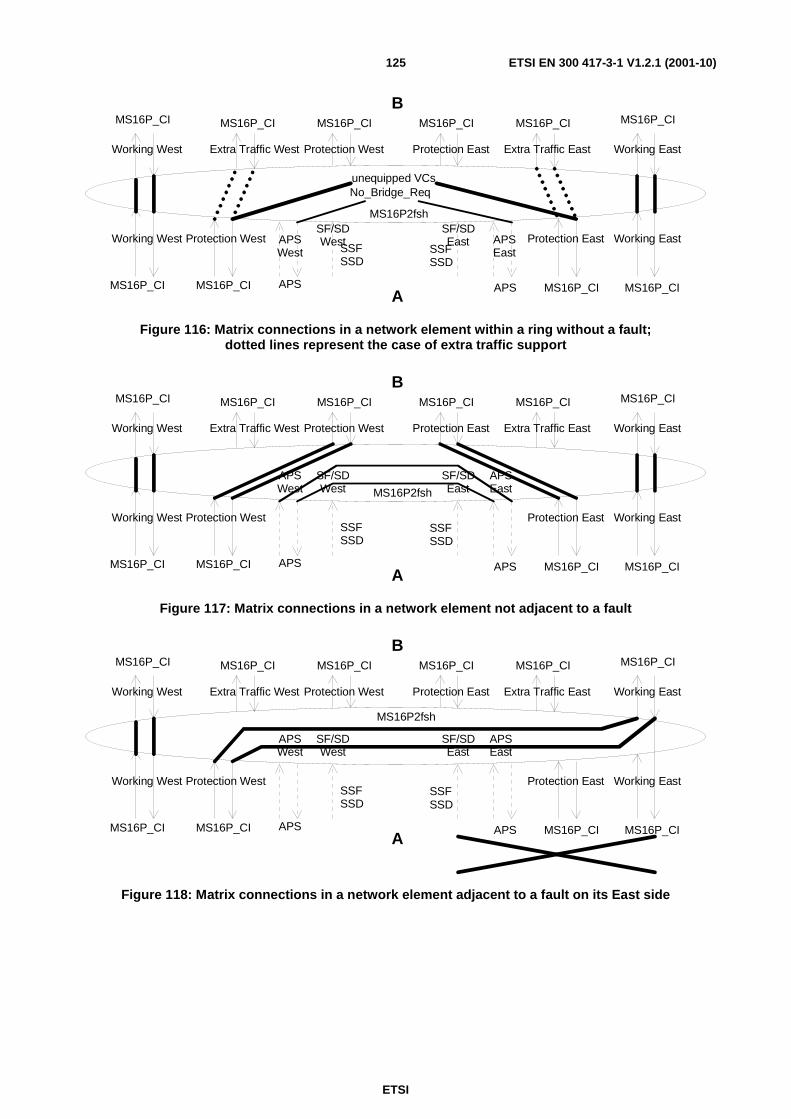
ETSI
ETSI EN 300 417-3-1 V1.2.1 (2001-10)125
MS16P_CI MS16P_CI
MS16P2fsh
APS
SSFSSD
Working West
APS
SSFSSD
Protection West
MS16P_CI
MS16P_CI MS16P_CI
Working West Extra Traffic West
Protection West
MS16P_CI
Working East
Protection East
MS16P_CI
MS16P_CIMS16P_CI
Working EastExtra Traffic East
Protection East
MS16P_CI
APSWest
SF/SDWest
SF/SDEast APS
East
A
B
unequipped VCsNo_Bridge_Req
Figure 116: Matrix connections in a network element within a ring without a fault; dotted lines represent the case of extra traffic support
MS16P_CI MS16P_CI
MS16P2fsh
APS
SSFSSD
Working West
APS
SSFSSD
Protection West
MS16P_CI
MS16P_CI MS16P_CI
Working West Extra Traffic West
Protection West
MS16P_CI
Working East
Protection East
MS16P_CI
MS16P_CIMS16P_CI
Working EastExtra Traffic East
Protection East
MS16P_CI
APSWest
SF/SDWest
SF/SDEast
APSEast
A
B
Figure 117: Matrix connections in a network element not adjacent to a fault
MS16P_CI MS16P_CI
MS16P2fsh
APS
SSFSSD
Working West
APS
SSFSSD
Protection West
MS16P_CI
MS16P_CI MS16P_CI
Working West Extra Traffic West
Protection West
MS16P_CI
Working East
Protection East
MS16P_CI
MS16P_CIMS16P_CI
Working EastExtra Traffic East
Protection East
MS16P_CI
APSWest
SF/SDWest
SF/SDEast
APSEast
A
B
Figure 118: Matrix connections in a network element adjacent to a fault on its East side
ETSI
ETSI EN 300 417-3-1 V1.2.1 (2001-10)126
MS16P_CI MS16P_CI
MS16P2fsh
APS
SSFSSD
Working West
APS
SSFSSD
Protection West
MS16P_CI
MS16P_CI MS16P_CI
Working West Extra Traffic West
Protection West
MS16P_CI
Working East
Protection East
MS16P_CI
MS16P_CIMS16P_CI
Working EastExtra Traffic East
Protection East
MS16P_CI
APSWest
SF/SDWest
SF/SDEast
APSEast
A
B
Figure 119: Matrix connections in a network element adjacent to a fault on its west side
MS Protection Operation: The 2 fibre MS shared protection ring trail protection process shall operate as specified in ETS 300 746 [6].
Defects:
For further study.
Consequent Actions:
The function shall generate a VC-4 [VC-4-4c] unequipped signal (plus valid AU-4 [AU-4-4c] pointer) for each protection timeslot when the protection timeslot is not in use.
The function shall insert all-ONEs (AIS) (squelching) for an AU-4 [AU-4-4c] within protection timeslots that would otherwise be misconnected.
Defect Correlations:
For further study.
Performance Monitoring:
For further study.
ETSI
ETSI EN 300 417-3-1 V1.2.1 (2001-10)127
9.6.2 STM-16 Multiplex Section 2 Fibre Shared Protection Ring Trail Termination Functions
9.6.2.1 STM-16 Multiplex Section 2 Fibre Shared Protection Ring Trail Termination Source MS16P2fsh_TT_So
Symbol:
MS16P2fsh
MS16_AI
MS16P2fsh_CI
Figure 120: MS16P2fsh_TT_So symbol
Interfaces:
Table 90: MS16P2fsh_TT_So input and output signals
Input(s) Output(s) MS16P2fsh_AI_D MS16P2fsh_AI_CK MS16P2fsh_AI_FS
MS16P2fsh_CI_D MS16P2fsh_CI_CK MS16P2fsh_CI_FS
Processes:
No information processing is required in the MS16P2fsh_TT_So, the MS16_AI at its output being identical to the MS16P2fsh_CI at its input.
Defects: None.
Consequent Actions: None.
Defect Correlations: None.
Performance Monitoring: None.
ETSI
ETSI EN 300 417-3-1 V1.2.1 (2001-10)128
9.6.2.2 STM-16 Multiplex Section 2 Fibre Shared Protection Ring Trail Termination Sink MS16P2fsh_TT_Sk
Symbol:
MS16P2fsh
MS16_AI
MS16P2fsh_CI
MS16P2fsh_TT_So_MI
Figure 121: MS16P2fsh_TT_Sk symbol
Interfaces:
Table 91: MS16P2fsh_TT_Sk input and output signals
Input(s) Output(s) MS16P2fsh_CI_D MS16P2fsh_CI_CK MS16P2fsh_CI_FS MS16P2fsh_CI_SSF MS16P2fsh_TT_Sk_MI_SSF_Reported
MS16_AI_D MS16_AI_CK MS16_AI_FS MS16_AI_TSF MS16P2fsh_TT_Sk_MI_cSSF
Processes:
The MS16P2fsh_TT_Sk function reports, as part of the MS16 layer, the state of the protected MS16 trail. In case all connections are unavailable the MS16P2fsh_TT_Sk reports the signal fail condition of the protected trail. This is applicable only for the working capacity.
Defects: None.
Consequent Actions:
aTSF ← CI_SSF.
Defect Correlations:
cSSF ← CI_SSF and SSF_Reported.
Performance Monitoring: None.
ETSI
ETSI EN 300 417-3-1 V1.2.1 (2001-10)129
9.6.3 STM-16 Multiplex Section 2 Fibre Shared Protection Ring Adaptation Functions
9.6.3.1 STM-16 Multiplex Section to STM-16 Multiplex Section 2 Fibre Shared Protection Ring Adaptation Source MS16/MS16P2fsh_A_So
Symbol:
MS16/MS16P2fsh
MS16P2fsh_CI
MS16_AI
Dw CK FS APSDp
Figure 122: MS16/MS16P2fsh_A_So symbol
Interfaces:
Table 92: MS16/MS16P2fsh_A_So input and output signals
Input(s) Output(s) MS16P2fsh_CI_Dw MS16P2fsh_CI_Dp MS16P2fsh_CI_CK MS16P2fsh_CI_FS MS16P2fsh_CI_APS
MS16_AI_D MS16_AI_CK MS16_AI_FS
Processes:
The function shall multiplex two groups of signals (CI_Dw, CI_Dp) into the MS16 payload (16 AU-4 timeslots). The working group signal shall be multiplexed into AU-4 timeslots 1 to 8 and the protection group signal shall be multiplexed into AU-4 timeslots 9 to 16.
The function shall map the MS16 2 fibre shared protection ring APS signal into bytes K1 and K2.
Defects: None.
Consequent actions: None.
Defect Correlations: None.
Performance Monitoring: None.
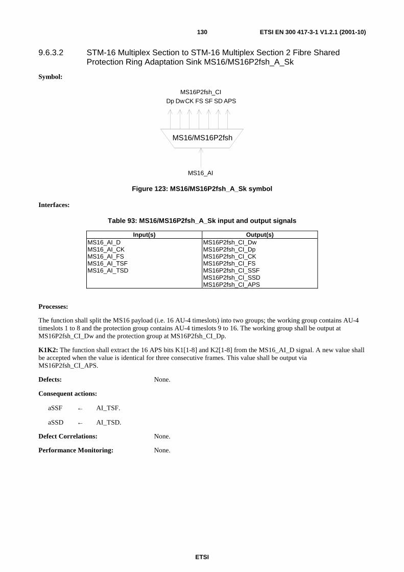
ETSI
ETSI EN 300 417-3-1 V1.2.1 (2001-10)130
9.6.3.2 STM-16 Multiplex Section to STM-16 Multiplex Section 2 Fibre Shared Protection Ring Adaptation Sink MS16/MS16P2fsh_A_Sk
Symbol:
MS16/MS16P2fsh
MS16P2fsh_CI
MS16_AI
DwCK FS SF SD APSDp
Figure 123: MS16/MS16P2fsh_A_Sk symbol
Interfaces:
Table 93: MS16/MS16P2fsh_A_Sk input and output signals
Input(s) Output(s) MS16_AI_D MS16_AI_CK MS16_AI_FS MS16_AI_TSF MS16_AI_TSD
MS16P2fsh_CI_Dw MS16P2fsh_CI_Dp MS16P2fsh_CI_CK MS16P2fsh_CI_FS MS16P2fsh_CI_SSF MS16P2fsh_CI_SSD MS16P2fsh_CI_APS
Processes:
The function shall split the MS16 payload (i.e. 16 AU-4 timeslots) into two groups; the working group contains AU-4 timeslots 1 to 8 and the protection group contains AU-4 timeslots 9 to 16. The working group shall be output at MS16P2fsh_CI_Dw and the protection group at MS16P2fsh_CI_Dp.
K1K2: The function shall extract the 16 APS bits K1[1-8] and K2[1-8] from the MS16_AI_D signal. A new value shall be accepted when the value is identical for three consecutive frames. This value shall be output via MS16P2fsh_CI_APS.
Defects: None.
Consequent actions:
aSSF ← AI_TSF.
aSSD ← AI_TSD.
Defect Correlations: None.
Performance Monitoring: None.
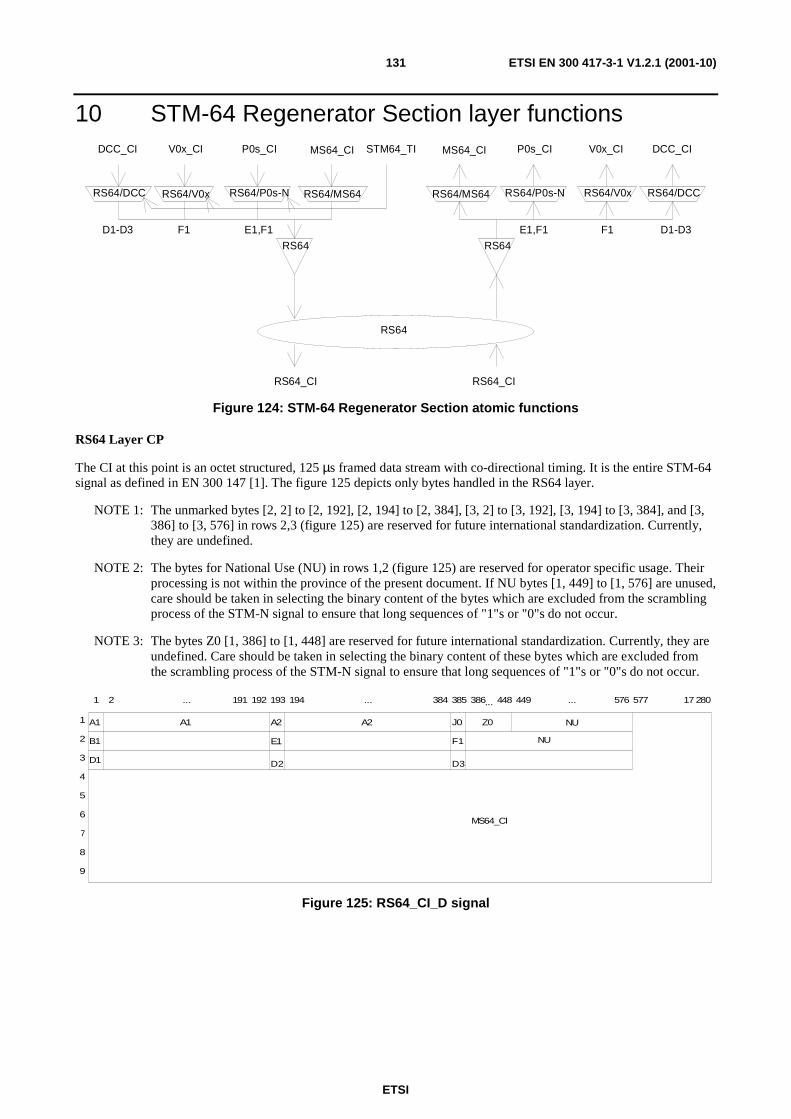
ETSI
ETSI EN 300 417-3-1 V1.2.1 (2001-10)131
10 STM-64 Regenerator Section layer functions
RS64
RS64/MS64
RS64
RS64/MS64
MS64_CI MS64_CI
RS64_CI RS64_CI
RS64/V0x RS64/V0xRS64/P0s-N
P0s_CISTM64_TI
RS64/P0s-N
P0s_CI
E1,F1 E1,F1
V0x_CIV0x_CI
RS64/DCC
DCC_CI
F1 D1-D3
RS64/DCC
DCC_CI
D1-D3 F1
RS64
Figure 124: STM-64 Regenerator Section atomic functions
RS64 Layer CP
The CI at this point is an octet structured, 125 µs framed data stream with co-directional timing. It is the entire STM-64 signal as defined in EN 300 147 [1]. The figure 125 depicts only bytes handled in the RS64 layer.
NOTE 1: The unmarked bytes [2, 2] to [2, 192], [2, 194] to [2, 384], [3, 2] to [3, 192], [3, 194] to [3, 384], and [3, 386] to [3, 576] in rows 2,3 (figure 125) are reserved for future international standardization. Currently, they are undefined.
NOTE 2: The bytes for National Use (NU) in rows 1,2 (figure 125) are reserved for operator specific usage. Their processing is not within the province of the present document. If NU bytes [1, 449] to [1, 576] are unused, care should be taken in selecting the binary content of the bytes which are excluded from the scrambling process of the STM-N signal to ensure that long sequences of "1"s or "0"s do not occur.
NOTE 3: The bytes Z0 [1, 386] to [1, 448] are reserved for future international standardization. Currently, they are undefined. Care should be taken in selecting the binary content of these bytes which are excluded from the scrambling process of the STM-N signal to ensure that long sequences of "1"s or "0"s do not occur.
A1
B1
D1
A1 A2
E1
D2
A2 J0 Z0
F1
D3
1
2
3
4
5
6
7
8
9
NU
1 2 ... 191 192 193 194 ... 384 385 386 448 449 ... 576 577 17 280
MS64_CI
NU
...
Figure 125: RS64_CI_D signal
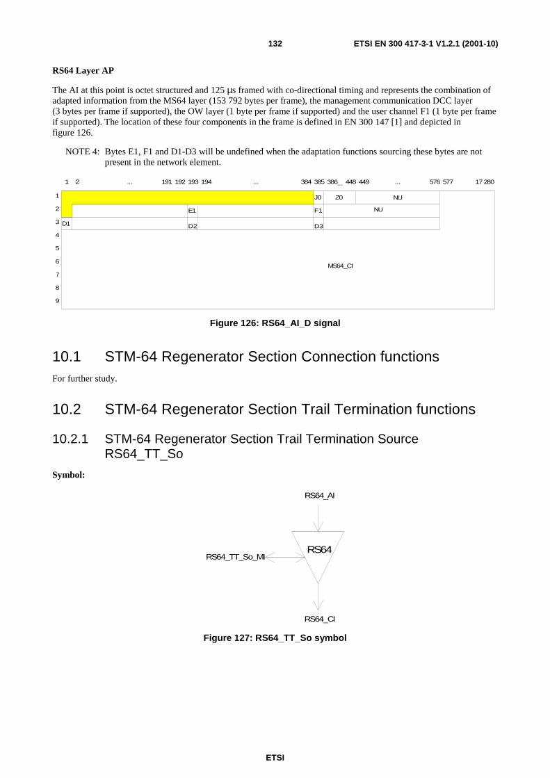
ETSI
ETSI EN 300 417-3-1 V1.2.1 (2001-10)132
RS64 Layer AP
The AI at this point is octet structured and 125 µs framed with co-directional timing and represents the combination of adapted information from the MS64 layer (153 792 bytes per frame), the management communication DCC layer (3 bytes per frame if supported), the OW layer (1 byte per frame if supported) and the user channel F1 (1 byte per frame if supported). The location of these four components in the frame is defined in EN 300 147 [1] and depicted in figure 126.
NOTE 4: Bytes E1, F1 and D1-D3 will be undefined when the adaptation functions sourcing these bytes are not present in the network element.
D1
E1
D2
J0 Z0
F1
D3
1
2
3
4
5
6
7
8
9
NU
1 2 ... 191 192 193 194 ... 384 385 386 448 449 ... 576 577 17 280
MS64_CI
NU
...
Figure 126: RS64_AI_D signal
10.1 STM-64 Regenerator Section Connection functions For further study.
10.2 STM-64 Regenerator Section Trail Termination functions
10.2.1 STM-64 Regenerator Section Trail Termination Source RS64_TT_So
Symbol:
RS64
RS64_AI
RS64_CI
RS64_TT_So_MI
Figure 127: RS64_TT_So symbol

ETSI
ETSI EN 300 417-3-1 V1.2.1 (2001-10)133
Interfaces:
Table 94: RS64_TT_So input and output signals
Input(s) Output(s) RS64_AI_D RS64_AI_CK RS64_AI_FS RS64_TT_So_MI_TxTI
RS64_CI_D RS64_CI_CK
Processes:
The function builds the STM-64 signal by adding the frame alignment information, bytes A1A2, the STM Section Trace Identifier (STI) byte J0, computing the parity and inserting the B1 byte.
J0: In this byte the function shall insert the Transmitted Trail Trace Identifier TxTI. Its format is described in EN 300 417-1-1 [3], clause 7.1.
B1: The function shall calculate a Bit Interleaved Parity 8 (BIP-8) code using even parity. The BIP-8 shall be calculated over all bits of the previous STM-64 frame after scrambling and is placed in byte position B1 of the current STM-64 frame before scrambling (figure 128).
A1A2: The function shall insert the STM-64 frame alignment signal A1...A1A2...A2 into the regenerator section overhead as defined in EN 300 147 [1] and depicted in figure 125.
Scrambler: This function provides scrambling of the RS64_CI. The operation of the scrambler shall be functionally identical to that of a frame synchronous scrambler of sequence length 127 operating at the line rate. The generating polynomial shall be 1 + X6 + X7. The scrambler shall be reset to "1111 1111" on the most significant bit (MSB) of the byte [1, 577] following the last byte of the STM-64 SOH in the first row. This bit and all subsequent bits to be scrambled shall be modulo 2 added to the output of the X7 position of the scrambler. The scrambler shall run continuously throughout the remaining STM-64 frame.
SCRAMBLER
BIP-8COMPUTATIONB1
RS64_CI
RS TRACE IDINSERTIONJ0
FAS INSERTION
RS64_AI
A1A2
TxTI
Figure 128: Some processes within RS64_TT_So

ETSI
ETSI EN 300 417-3-1 V1.2.1 (2001-10)134
Defects: None.
Consequent Actions: None.
Defect Correlations: None.
Performance Monitoring: None.
10.2.2 STM-64 Regenerator Section Trail Termination Sink RS64_TT_Sk
Symbol:
RS64
RS64_AI
RS64_CI
RS64_TT_Sk_MI
Figure 129: RS64_TT_Sk symbol
Interfaces:
Table 95: RS64_TT_Sk input and output signals
Input(s) Output(s) RS64_CI_D RS64_CI_CK RS64_CI_FS RS64_CI_SSF RS64_TT_Sk_MI_ExTI RS64_TT_Sk_MI_TPmode RS64_TT_Sk_MI_TIMdis RS64_TT_Sk_MI_ExTImode RS64_TT_Sk_MI_1second
RS64_AI_D RS64_AI_CK RS64_AI_FS RS64_AI_TSF RS64_TT_Sk_MI_AcTI RS64_TT_Sk_MI_cTIM RS64_TT_Sk_MI_pN_EBC RS64_TT_Sk_MI_pN_DS
Processes:
This function monitors the STM-64 signal for RS errors, and recovers the RS trail termination status. It extracts the payload independent overhead bytes (J0, B1) from the RS64 layer Characteristic Information:
Descrambling: The function shall descramble the incoming STM-64 signal. The operation of the descrambler shall be functionally identical to that of a scrambler in RS64_TT_So.
B1: Even bit parity is computed for each bit n of every byte of the preceding scrambled STM-64 frame and compared with bit n of B1 recovered from the current frame (n = 1 to 8 inclusive) (figure 130). A difference between the computed and recovered B1 values is taken as evidence of one or more errors (nN_B) in the computation block.
J0: The Received Trail Trace Identifier RxTI shall be recovered from the J0 byte and shall be made available as AcTI for network management purposes. The application and acceptance and mismatch detection process shall be performed as specified in EN 300 417-1-1 [3], clauses 7.1 and 8.2.1.3.
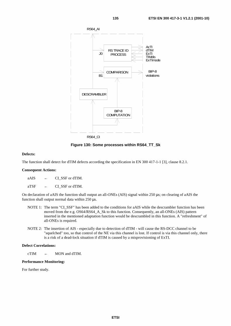
ETSI
ETSI EN 300 417-3-1 V1.2.1 (2001-10)135
DESCRAMBLER
BIP-8COMPUTATION
B1
RS TRACE IDPROCESSJ0
RS64_CI
COMPARISON BIP-8violations
AcTIdTIMExTI
RS64_AI
TIMdisExTImode
Figure 130: Some processes within RS64_TT_Sk
Defects:
The function shall detect for dTIM defects according the specification in EN 300 417-1-1 [3], clause 8.2.1.
Consequent Actions:
aAIS ← CI_SSF or dTIM.
aTSF ← CI_SSF or dTIM.
On declaration of aAIS the function shall output an all-ONEs (AIS) signal within 250 µs; on clearing of aAIS the function shall output normal data within 250 µs.
NOTE 1: The term "CI_SSF" has been added to the conditions for aAIS while the descrambler function has been moved from the e.g. OS64/RS64_A_Sk to this function. Consequently, an all-ONEs (AIS) pattern inserted in the mentioned adaptation function would be descrambled in this function. A "refreshment" of all-ONEs is required.
NOTE 2: The insertion of AIS - especially due to detection of dTIM - will cause the RS-DCC channel to be "squelched" too, so that control of the NE via this channel is lost. If control is via this channel only, there is a risk of a dead-lock situation if dTIM is caused by a misprovisioning of ExTI.
Defect Correlations:
cTIM ← MON and dTIM.
Performance Monitoring:
For further study.
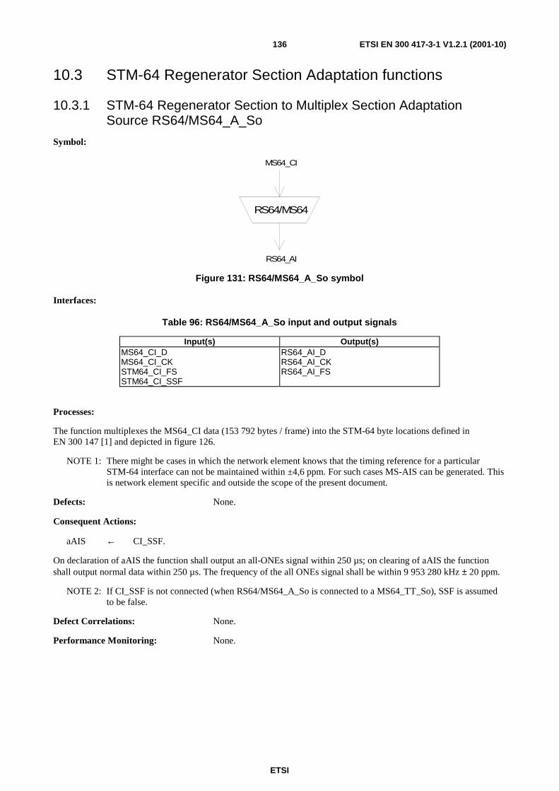
ETSI
ETSI EN 300 417-3-1 V1.2.1 (2001-10)136
10.3 STM-64 Regenerator Section Adaptation functions
10.3.1 STM-64 Regenerator Section to Multiplex Section Adaptation Source RS64/MS64_A_So
Symbol:
RS64/MS64
MS64_CI
RS64_AI
Figure 131: RS64/MS64_A_So symbol
Interfaces:
Table 96: RS64/MS64_A_So input and output signals
Input(s) Output(s) MS64_CI_D MS64_CI_CK STM64_CI_FS STM64_CI_SSF
RS64_AI_D RS64_AI_CK RS64_AI_FS
Processes:
The function multiplexes the MS64_CI data (153 792 bytes / frame) into the STM-64 byte locations defined in EN 300 147 [1] and depicted in figure 126.
NOTE 1: There might be cases in which the network element knows that the timing reference for a particular STM-64 interface can not be maintained within ±4,6 ppm. For such cases MS-AIS can be generated. This is network element specific and outside the scope of the present document.
Defects: None.
Consequent Actions:
aAIS ← CI_SSF.
On declaration of aAIS the function shall output an all-ONEs signal within 250 µs; on clearing of aAIS the function shall output normal data within 250 µs. The frequency of the all ONEs signal shall be within 9 953 280 kHz ± 20 ppm.
NOTE 2: If CI_SSF is not connected (when RS64/MS64_A_So is connected to a MS64_TT_So), SSF is assumed to be false.
Defect Correlations: None.
Performance Monitoring: None.

ETSI
ETSI EN 300 417-3-1 V1.2.1 (2001-10)137
10.3.2 STM-64 Regenerator Section to Multiplex Section Adaptation Sink RS64/MS64_A_Sk
Symbol:
RS64/MS64
MS64_CI
RS64_AI
Figure 132: RS64/MS64_A_Sk symbol
Interfaces:
Table 97: RS64/MS64_A_Sk input and output signals
Input(s) Output(s) RS64_AI_D RS64_AI_CK RS64_AI_FS RS64_AI_TSF
MS64_CI_D MS64_CI_CK MS64_CI_FS MS64_CI_SSF
Processes:
The function separates MS64_CI data from RS64_AI as depicted in figure 126.
Defects: None.
Consequent Actions:
aSSF ← AI_TSF.
Defect Correlations: None.
Performance Monitoring: None.
10.3.3 STM-64 Regenerator Section to DCC Adaptation Source RS64/DCC_A_So
Symbol:
RS64/DCC
DCC_CI_D
RS64_AI
STM64_TI
DCC_CI_CK
Figure 133: RS64/DCC_A_So symbol

ETSI
ETSI EN 300 417-3-1 V1.2.1 (2001-10)138
Interfaces:
Table 98: RS64/DCC_A_So input and output signals
Input(s) Output(s) DCC_CI_D STM64_TI_CK STM64_TI_FS
RS64_AI_D DCC_CI_CK
Processes:
The function multiplexes the DCC CI data (192 kbit/s) into the byte locations D1, D2 and D3 as defined in EN 300 147 [1] and depicted in figure 126.
NOTE: DCC transmission can be "disabled" when the matrix connection in the connected DCC_C function is removed.
Defects: None.
Consequent Actions: None.
Defect Correlations: None.
Performance Monitoring: None.
10.3.4 STM-64 Regenerator Section to DCC Adaptation Sink RS64/DCC_A_Sk
Symbol:
RS64/DCC
DCC_CI
RS64_AI
Figure 134: RS64/DCC_A_Sk symbol
Interfaces:
Table 99: RS64/DCC_A_Sk input and output signals
Input(s) Output(s) RS64_AI_D RS64_AI_CK RS64_AI_FS RS64_AI_TSF
DCC_CI_D DCC_CI_CK DCC_CI_SSF
Processes:
The function separates DCC data from RS Overhead as defined in EN 300 147 [1] and depicted in figure 126.
NOTE: DCC transmission can be "disabled" when the matrix connection in the connected DCC_C function is removed.
Defects: None.
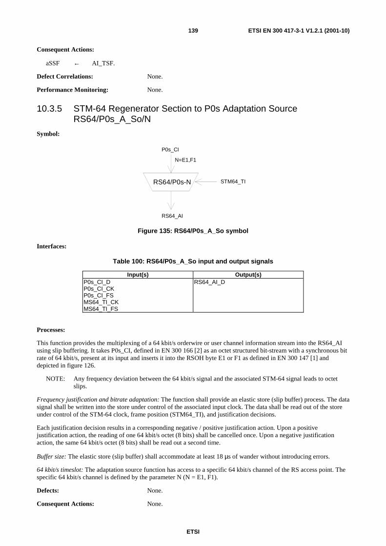
ETSI
ETSI EN 300 417-3-1 V1.2.1 (2001-10)139
Consequent Actions:
aSSF ← AI_TSF.
Defect Correlations: None.
Performance Monitoring: None.
10.3.5 STM-64 Regenerator Section to P0s Adaptation Source RS64/P0s_A_So/N
Symbol:
RS64/P0s-N
P0s_CI
RS64_AI
STM64_TI
N=E1,F1
Figure 135: RS64/P0s_A_So symbol
Interfaces:
Table 100: RS64/P0s_A_So input and output signals
Input(s) Output(s) P0s_CI_D P0s_CI_CK P0s_CI_FS MS64_TI_CK MS64_TI_FS
RS64_AI_D
Processes:
This function provides the multiplexing of a 64 kbit/s orderwire or user channel information stream into the RS64_AI using slip buffering. It takes P0s_CI, defined in EN 300 166 [2] as an octet structured bit-stream with a synchronous bit rate of 64 kbit/s, present at its input and inserts it into the RSOH byte E1 or F1 as defined in EN 300 147 [1] and depicted in figure 126.
NOTE: Any frequency deviation between the 64 kbit/s signal and the associated STM-64 signal leads to octet slips.
Frequency justification and bitrate adaptation: The function shall provide an elastic store (slip buffer) process. The data signal shall be written into the store under control of the associated input clock. The data shall be read out of the store under control of the STM-64 clock, frame position (STM64_TI), and justification decisions.
Each justification decision results in a corresponding negative / positive justification action. Upon a positive justification action, the reading of one 64 kbit/s octet (8 bits) shall be cancelled once. Upon a negative justification action, the same 64 kbit/s octet (8 bits) shall be read out a second time.
Buffer size: The elastic store (slip buffer) shall accommodate at least 18 µs of wander without introducing errors.
64 kbit/s timeslot: The adaptation source function has access to a specific 64 kbit/s channel of the RS access point. The specific 64 kbit/s channel is defined by the parameter N (N = E1, F1).
Defects: None.
Consequent Actions: None.
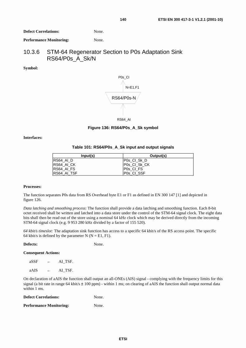
ETSI
ETSI EN 300 417-3-1 V1.2.1 (2001-10)140
Defect Correlations: None.
Performance Monitoring: None.
10.3.6 STM-64 Regenerator Section to P0s Adaptation Sink RS64/P0s_A_Sk/N
Symbol:
RS64/P0s-N
P0s_CI
RS64_AI
N=E1,F1
Figure 136: RS64/P0s_A_Sk symbol
Interfaces:
Table 101: RS64/P0s_A_Sk input and output signals
Input(s) Output(s) RS64_AI_D RS64_AI_CK RS64_AI_FS RS64_AI_TSF
P0s_CI_Sk_D P0s_CI_Sk_CK P0s_CI_FS P0s_CI_SSF
Processes:
The function separates P0s data from RS Overhead byte E1 or F1 as defined in EN 300 147 [1] and depicted in figure 126.
Data latching and smoothing process: The function shall provide a data latching and smoothing function. Each 8-bit octet received shall be written and latched into a data store under the control of the STM-64 signal clock. The eight data bits shall then be read out of the store using a nominal 64 kHz clock which may be derived directly from the incoming STM-64 signal clock (e.g. 9 953 280 kHz divided by a factor of 155 520).
64 kbit/s timeslot: The adaptation sink function has access to a specific 64 kbit/s of the RS access point. The specific 64 kbit/s is defined by the parameter N (N = E1, F1).
Defects: None.
Consequent Actions:
aSSF ← AI_TSF.
aAIS ← AI_TSF.
On declaration of aAIS the function shall output an all-ONEs (AIS) signal - complying with the frequency limits for this signal (a bit rate in range 64 kbit/s ± 100 ppm) - within 1 ms; on clearing of aAIS the function shall output normal data within 1 ms.
Defect Correlations: None.
Performance Monitoring: None.

ETSI
ETSI EN 300 417-3-1 V1.2.1 (2001-10)141
10.3.7 STM-64 Regenerator Section to V0x Adaptation Source RS64/V0x_A_So
Symbol:
RS64/V0x
RS64_AI
STM64_TI
V0x_CI_D V0x_CI_CK
Figure 137: RS64/V0x_A_So symbol
Interfaces:
Table 102: RS64/V0x_A_So input and output signals
Input(s) Output(s) V0x_CI_D STM64_TI_CK STM64_TI_FS
RS64_AI_D V0x_CI_CK
Processes: None.
This function multiplexes the V0x_CI data (64 kbit/s) into the byte location F1 as defined in EN 300 147 [1] and depicted in figure 126.
The user channel byte F1 shall be added to the 125 µs frame.
Defects: None.
Consequent Actions: None.
Defect Correlations: None.
Performance Monitoring: None.
10.3.8 STM-64 Regenerator Section to V0x Adaptation Sink RS64/V0x_A_Sk
Symbol:
RS64/V0x
V0x_CI
RS64_AI
Figure 138: RS64/V0x_A_Sk symbol
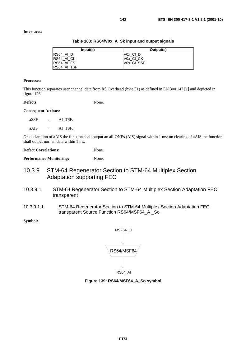
ETSI
ETSI EN 300 417-3-1 V1.2.1 (2001-10)142
Interfaces:
Table 103: RS64/V0x_A_Sk input and output signals
Input(s) Output(s) RS64_AI_D RS64_AI_CK RS64_AI_FS RS64_AI_TSF
V0x_CI_D V0x_CI_CK V0x_CI_SSF
Processes:
This function separates user channel data from RS Overhead (byte F1) as defined in EN 300 147 [1] and depicted in figure 126.
Defects: None.
Consequent Actions:
aSSF ← AI_TSF.
aAIS ← AI_TSF.
On declaration of aAIS the function shall output an all-ONEs (AIS) signal within 1 ms; on clearing of aAIS the function shall output normal data within 1 ms.
Defect Correlations: None.
Performance Monitoring: None.
10.3.9 STM-64 Regenerator Section to STM-64 Multiplex Section Adaptation supporting FEC
10.3.9.1 STM-64 Regenerator Section to STM-64 Multiplex Section Adaptation FEC transparent
10.3.9.1.1 STM-64 Regenerator Section to STM-64 Multiplex Section Adaptation FEC transparent Source Function RS64/MSF64_A _So
Symbol:
RS64/MSF64
MSF64_CI
RS64_AI
Figure 139: RS64/MSF64_A_So symbol
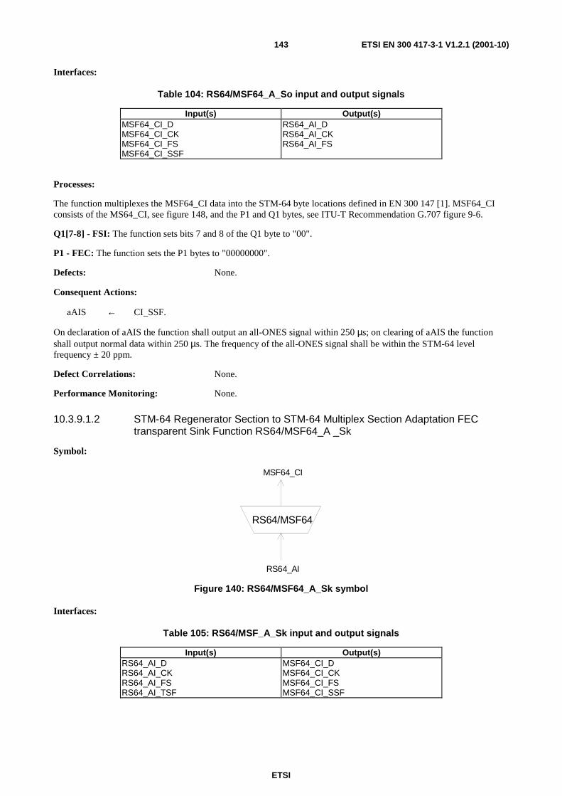
ETSI
ETSI EN 300 417-3-1 V1.2.1 (2001-10)143
Interfaces:
Table 104: RS64/MSF64_A_So input and output signals
Input(s) Output(s) MSF64_CI_D MSF64_CI_CK MSF64_CI_FS MSF64_CI_SSF
RS64_AI_D RS64_AI_CK RS64_AI_FS
Processes:
The function multiplexes the MSF64_CI data into the STM-64 byte locations defined in EN 300 147 [1]. MSF64_CI consists of the MS64_CI, see figure 148, and the P1 and Q1 bytes, see ITU-T Recommendation G.707 figure 9-6.
Q1[7-8] - FSI: The function sets bits 7 and 8 of the Q1 byte to "00".
P1 - FEC: The function sets the P1 bytes to "00000000".
Defects: None.
Consequent Actions:
aAIS ← CI_SSF.
On declaration of aAIS the function shall output an all-ONES signal within 250 µs; on clearing of aAIS the function shall output normal data within 250 µs. The frequency of the all-ONES signal shall be within the STM-64 level frequency ± 20 ppm.
Defect Correlations: None.
Performance Monitoring: None.
10.3.9.1.2 STM-64 Regenerator Section to STM-64 Multiplex Section Adaptation FEC transparent Sink Function RS64/MSF64_A _Sk
Symbol:
RS64/MSF64
MSF64_CI
RS64_AI
Figure 140: RS64/MSF64_A_Sk symbol
Interfaces:
Table 105: RS64/MSF_A_Sk input and output signals
Input(s) Output(s) RS64_AI_D RS64_AI_CK RS64_AI_FS RS64_AI_TSF
MSF64_CI_D MSF64_CI_CK MSF64_CI_FS MSF64_CI_SSF
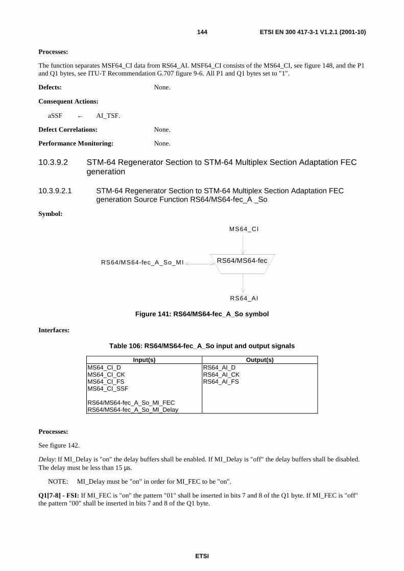
ETSI
ETSI EN 300 417-3-1 V1.2.1 (2001-10)144
Processes:
The function separates MSF64_CI data from RS64_AI. MSF64_CI consists of the MS64_CI, see figure 148, and the P1 and Q1 bytes, see ITU-T Recommendation G.707 figure 9-6. All P1 and Q1 bytes set to "1".
Defects: None.
Consequent Actions:
aSSF ← AI_TSF.
Defect Correlations: None.
Performance Monitoring: None.
10.3.9.2 STM-64 Regenerator Section to STM-64 Multiplex Section Adaptation FEC generation
10.3.9.2.1 STM-64 Regenerator Section to STM-64 Multiplex Section Adaptation FEC generation Source Function RS64/MS64-fec_A _So
Symbol:
RS64/MS64-fec
MS64_CI
RS64_AI
RS64/MS64-fec_A_So_MI
Figure 141: RS64/MS64-fec_A_So symbol
Interfaces:
Table 106: RS64/MS64-fec_A_So input and output signals
Input(s) Output(s) MS64_CI_D MS64_CI_CK MS64_CI_FS MS64_CI_SSF RS64/MS64-fec_A_So_MI_FEC RS64/MS64-fec_A_So_MI_Delay
RS64_AI_D RS64_AI_CK RS64_AI_FS
Processes:
See figure 142.
Delay: If MI_Delay is "on" the delay buffers shall be enabled. If MI_Delay is "off" the delay buffers shall be disabled. The delay must be less than 15 µs.
NOTE: MI_Delay must be "on" in order for MI_FEC to be "on".
Q1[7-8] - FSI: If MI_FEC is "on" the pattern "01" shall be inserted in bits 7 and 8 of the Q1 byte. If MI_FEC is "off" the pattern "00" shall be inserted in bits 7 and 8 of the Q1 byte.
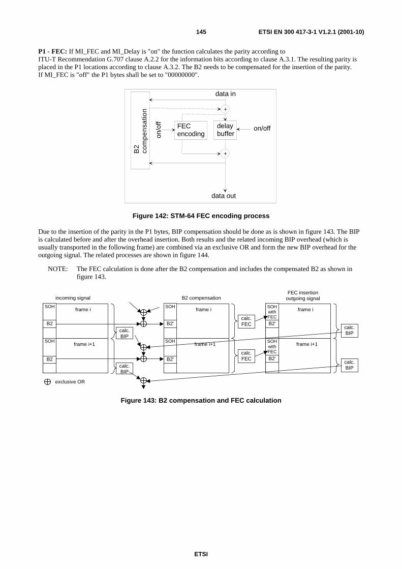
ETSI
ETSI EN 300 417-3-1 V1.2.1 (2001-10)145
P1 - FEC: If MI_FEC and MI_Delay is "on" the function calculates the parity according to ITU-T Recommendation G.707 clause A.2.2 for the information bits according to clause A.3.1. The resulting parity is placed in the P1 locations according to clause A.3.2. The B2 needs to be compensated for the insertion of the parity. If MI_FEC is "off" the P1 bytes shall be set to "00000000".
data in
delaybuffer
FECencoding
B2
com
pe
nsa
tion
data out
on/off
on/o
ff+
+
Figure 142: STM-64 FEC encoding process
Due to the insertion of the parity in the P1 bytes, BIP compensation should be done as is shown in figure 143. The BIP is calculated before and after the overhead insertion. Both results and the related incoming BIP overhead (which is usually transported in the following frame) are combined via an exclusive OR and form the new BIP overhead for the outgoing signal. The related processes are shown in figure 144.
NOTE: The FEC calculation is done after the B2 compensation and includes the compensated B2 as shown in figure 143.
frame i
frame i+1
calc.BIP
frame i
frame i+1
calc.FEC
incoming signal B2 compensation
exclusive OR
SOH SOH
B2 B2'
frame i
frame i+1
calc.BIP
FEC insertionoutgoing signal
SOHwithFEC
SOHwithFEC
B2'
B2'calc.FEC
SOH
calc.BIP
calc.BIP
B2
SOH
B2'
Figure 143: B2 compensation and FEC calculation
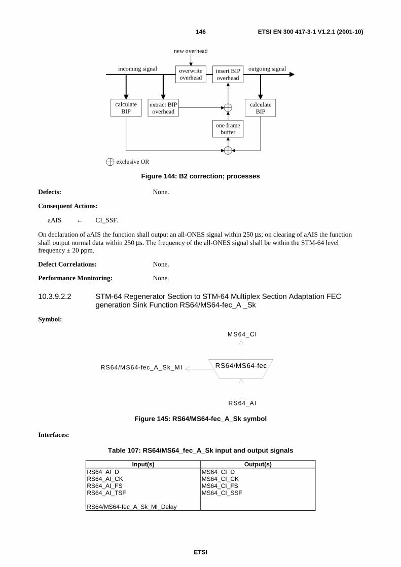
ETSI
ETSI EN 300 417-3-1 V1.2.1 (2001-10)146
new overhead
incoming signal outgoing signal
exclusive OR
overwrite overhead
insert BIP overhead
calculate BIP
extract BIP overhead
calculate BIP
one frame buffer
Figure 144: B2 correction; processes
Defects: None.
Consequent Actions:
aAIS ← CI_SSF.
On declaration of aAIS the function shall output an all-ONES signal within 250 µs; on clearing of aAIS the function shall output normal data within 250 µs. The frequency of the all-ONES signal shall be within the STM-64 level frequency ± 20 ppm.
Defect Correlations: None.
Performance Monitoring: None.
10.3.9.2.2 STM-64 Regenerator Section to STM-64 Multiplex Section Adaptation FEC generation Sink Function RS64/MS64-fec_A _Sk
Symbol:
RS64/MS64-fec
MS64_CI
RS64_AI
RS64/MS64-fec_A_Sk_MI
Figure 145: RS64/MS64-fec_A_Sk symbol
Interfaces:
Table 107: RS64/MS64_fec_A_Sk input and output signals
Input(s) Output(s) RS64_AI_D RS64_AI_CK RS64_AI_FS RS64_AI_TSF RS64/MS64-fec_A_Sk_MI_Delay
MS64_CI_D MS64_CI_CK MS64_CI_FS MS64_CI_SSF
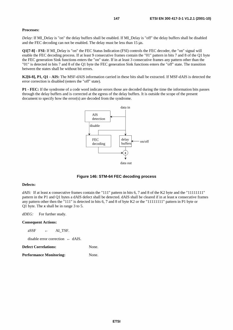
ETSI
ETSI EN 300 417-3-1 V1.2.1 (2001-10)147
Processes:
Delay: If MI_Delay is "on" the delay buffers shall be enabled. If MI_Delay is "off" the delay buffers shall be disabled and the FEC decoding can not be enabled. The delay must be less than 15 µs.
Q1[7-8] - FSI: If MI_Delay is "on" the FEC Status Indication (FSI) controls the FEC decoder, the "on" signal will enable the FEC decoding process. If at least 9 consecutive frames contain the "01" pattern in bits 7 and 8 of the Q1 byte the FEC generation Sink functions enters the "on" state. If in at least 3 consecutive frames any pattern other than the "01" is detected in bits 7 and 8 of the Q1 byte the FEC generation Sink functions enters the "off" state. The transition between the states shall be without bit errors.
K2[6-8], P1, Q1 - AIS: The MSF-dAIS information carried in these bits shall be extracted. If MSF-dAIS is detected the error correction is disabled (enters the "off" state).
P1 - FEC: If the syndrome of a code word indicate errors those are decoded during the time the information bits passes through the delay buffers and is corrected at the egress of the delay buffers. It is outside the scope of the present document to specify how the error(s) are decoded from the syndrome.
data in
data out
on/off
disable
AIS detection
FEC decoding
delay buffers
Figure 146: STM-64 FEC decoding process
Defects:
dAIS: If at least x consecutive frames contain the "111" pattern in bits 6, 7 and 8 of the K2 byte and the "11111111" pattern in the P1 and Q1 bytes a dAIS defect shall be detected. dAIS shall be cleared if in at least x consecutive frames any pattern other then the "111" is detected in bits 6, 7 and 8 of byte K2 or the "11111111" pattern in P1 byte or Q1 byte. The x shall be in range 3 to 5.
dDEG: For further study.
Consequent Actions:
aSSF ← AI_TSF.
disable error correction ← dAIS.
Defect Correlations: None.
Performance Monitoring: None.
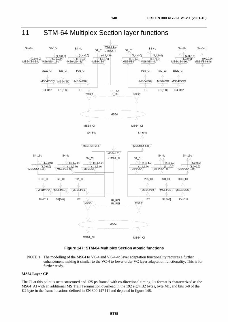
ETSI
ETSI EN 300 417-3-1 V1.2.1 (2001-10)148
11 STM-64 Multiplex Section layer functions
MS64_CI
P0s_CIP0s_CI
E2 E2
SD_CISD_CI DCC_CI
S1[5-8] D4-D12
MS64/DCC
DCC_CI
D4-D12 S1[5-8] RI_RDIRI_REI
S4_CIS4_CI
(1,1,1,0)
S4-4c S4-4c
MS64
MS64_CI
MS64MS64
MS64/SD MS64/P0s
MS64/S4MS64/S4-4cMS64/S4-16c
STM64_TI
MS64-LC
MS64/DCCMS64/SDMS64/P0s
MS64/S4 MS64/S4-4c MS64/S4-16c
MS64/S4-64c
(4,4,4,0)(4,4,0,0)(1,1,0,0)
(4,0,0,0)(1,0,0,0)
S4-16cS4-16c
(1,1,1,0)(4,4,4,0) (4,4,0,0)
(1,1,0,0)(4,0,0,0)
(1,0,0,0)
S4-64c
MS64/S4-64c
S4-64c
Figure 147: STM-64 Multiplex Section atomic functions
NOTE 1: The modelling of the MS64 to VC-4 and VC-4-4c layer adaptation functionality requires a further enhancement making it similar to the VC-4 to lower order VC layer adaptation functionality. This is for further study.
MS64 Layer CP
The CI at this point is octet structured and 125 µs framed with co-directional timing. Its format is characterized as the MS64_AI with an additional MS Trail Termination overhead in the 192 eight B2 bytes, byte M1, and bits 6-8 of the K2 byte in the frame locations defined in EN 300 147 [1] and depicted in figure 148.
MS64 MS64
MS64_CI MS64_CI
MS64/SD MS64/SDMS64/P0s
P0s_CI
STM64_TI
MS64/P0s
P0s_CI
E2 E2
SD_CISD_CI
MS64/DCC
DCC_CI
S1[5-8] D4-D12
MS64/DCC
DCC_CI
D4-D12 S1[5-8] RI_RDIRI_REI
S4_CI
MS64/S4
S4_CI
(1,1,1,0)(4,4,4,0)
S4-4c
MS64/S4(1,1,1,0)
(4,4,4,0)
S4-4c
MS64/S4-4c(1,1,0,0)
(4,4,0,0)
MS64/S4-4c(1,1,0,0)
(4,4,0,0)
MS64-LC
MS64
MS64/S4-64cMS64/S4-16c(1,0,0,0)
(4,0,0,0)(0,0,0,0)
S4-16c S4-64c
MS64/S4-16c(1,0,0,0)
(4,0,0,0)
S4-16c
MS64/S4-64c(0,0,0,0)
S4-64c
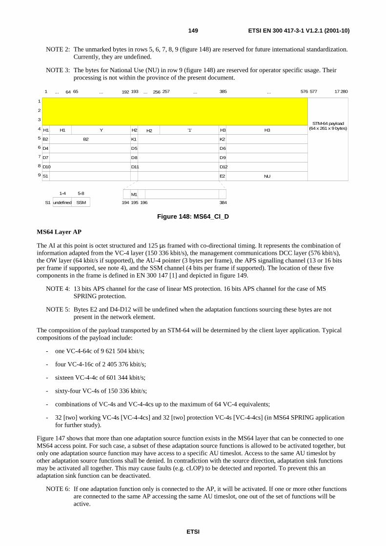
ETSI
ETSI EN 300 417-3-1 V1.2.1 (2001-10)149
NOTE 2: The unmarked bytes in rows 5, 6, 7, 8, 9 (figure 148) are reserved for future international standardization. Currently, they are undefined.
NOTE 3: The bytes for National Use (NU) in row 9 (figure 148) are reserved for operator specific usage. Their processing is not within the province of the present document.
B2
D4
D7
D10
S1
B2 K1
D5
D8
D11
M1
K2
D6
D9
D12
E2
1
2
3
4
5
6
7
8
9
H1 H1 H2 H3 H3
NU
'1'Y
1 65 193 257 385 576 577 17 280
STM-64 payload(64 x 261 x 9 bytes)
194 195 196 384
H2
19264 256... ... ... ... ...
SSMundefined
1-4 5-8
S1
Figure 148: MS64_CI_D
MS64 Layer AP
The AI at this point is octet structured and 125 µs framed with co-directional timing. It represents the combination of information adapted from the VC-4 layer (150 336 kbit/s), the management communications DCC layer (576 kbit/s), the OW layer (64 kbit/s if supported), the AU-4 pointer (3 bytes per frame), the APS signalling channel (13 or 16 bits per frame if supported, see note 4), and the SSM channel (4 bits per frame if supported). The location of these five components in the frame is defined in EN 300 147 [1] and depicted in figure 149.
NOTE 4: 13 bits APS channel for the case of linear MS protection. 16 bits APS channel for the case of MS SPRING protection.
NOTE 5: Bytes E2 and D4-D12 will be undefined when the adaptation functions sourcing these bytes are not present in the network element.
The composition of the payload transported by an STM-64 will be determined by the client layer application. Typical compositions of the payload include:
- one VC-4-64c of 9 621 504 kbit/s;
- four VC-4-16c of 2 405 376 kbit/s;
- sixteen VC-4-4c of 601 344 kbit/s;
- sixty-four VC-4s of 150 336 kbit/s;
- combinations of VC-4s and VC-4-4cs up to the maximum of 64 VC-4 equivalents;
- 32 [two] working VC-4s [VC-4-4cs] and 32 [two] protection VC-4s [VC-4-4cs] (in MS64 SPRING application for further study).
Figure 147 shows that more than one adaptation source function exists in the MS64 layer that can be connected to one MS64 access point. For such case, a subset of these adaptation source functions is allowed to be activated together, but only one adaptation source function may have access to a specific AU timeslot. Access to the same AU timeslot by other adaptation source functions shall be denied. In contradiction with the source direction, adaptation sink functions may be activated all together. This may cause faults (e.g. cLOP) to be detected and reported. To prevent this an adaptation sink function can be deactivated.
NOTE 6: If one adaptation function only is connected to the AP, it will be activated. If one or more other functions are connected to the same AP accessing the same AU timeslot, one out of the set of functions will be active.

ETSI
ETSI EN 300 417-3-1 V1.2.1 (2001-10)150
D4
D7
D10
S1
K1
D5
D8
D11
K2
D6
D9
D12
E2
1
2
3
4
5
6
7
8
9
H1 H1 H2 H3 H3
NU
'1'Y
1 65 193 257 385 576 577 17 280
STM-64 payload(64 x 261 x 9 bytes)
194 195 196 384
H2
19264 256... ... ... ... ...
SSMundefined
1-4 5-8
S1
Figure 149: MS64_AI_D
Figure 150 shows the MS trail protection specific sublayer atomic functions (MS64/MS64P_A, MS64P_C, MS64P_TT) within the MS64 layer. Note that the DCC (D4-D12), OW (E2), and SSM (S1[5-8]) signals can be accessible before (unprotected) and after (protected) the MS64P_C function. The choice is outside the scope of the present document.
NOTE 7: Equipment may provide MS protection and bi-directional services such as DCC and OW in the MS layer. Where a link uses this provision both ends of the link shall be configured to operate these services in the same mode (i.e. either protected or unprotected).
MS64
MS64/MS64P
MS64
MS64/MS64P
MS64P
MS64_CI MS64_CI
MS64/P0s
P0s_CI
STM16_TI
MS64/P0s
P0s_CI
E2 E2
MS64/DCC
DCC_CI
D4-D12
MS64/DCC
DCC_CI
D4-D12 RI_RDIRI_REI
MS64/S4-Xc
S4-Xc_CI
MS64/S4-Xc
S4-Xc_CI
MS64/SD
SD_CI
S1[5-8]MS64P MS64P
S4_CI
MS64/S4(1,1,1,0)(4,4,4,0)
MS64/P0sMS64/DCC
P0s_CIDCC_CI
MS64/P0s MS64/DCC
P0s_CI DCC_CI
MS64/SD
S1[5-8]
SD_CI
MS64/SD
S1[5-8]
SD_CI
MS64/SD
SD_CI
S1[5-8]
S4_CI
MS64/S4(1,1,1,0)(4,4,4,0)
Figure 150: STM-64 Multiplex Section Linear Trail Protection Functions
MS64P Sublayer CP
The CI at this point is octet structured and 125 µs framed with co-directional timing. Its format is equivalent to the MS4_AI and depicted in figure 151.
NOTE 8: Bytes S1, E2 and D4-D12 will be undefined when the adaptation functions sourcing these bytes are not present in the network element or are unprotected (see above).
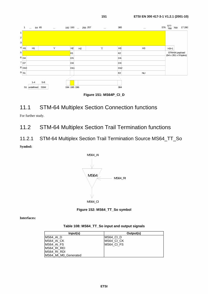
ETSI
ETSI EN 300 417-3-1 V1.2.1 (2001-10)151
D4
D7
D10
S1
K1
D5
D8
D11
K2
D6
D9
D12
E2
1
2
3
4
5
6
7
8
9
H1 H1 H2 H3 H3
NU
'1'Y
1 65 193 257 385 576577-768 17 280
STM-64 payload(64 x 261 x 9 bytes)
194 195 196 384
H2
19264 256... ... ... ... ...
SSMundefined
1-4 5-8
S1
H3+1
769
Figure 151: MS64P_CI_D
11.1 STM-64 Multiplex Section Connection functions For further study.
11.2 STM-64 Multiplex Section Trail Termination functions
11.2.1 STM-64 Multiplex Section Trail Termination Source MS64_TT_So
Symbol:
MS64
MS64_AI
MS64_CI
MS64_RI
Figure 152: MS64_TT_So symbol
Interfaces:
Table 108: MS64_TT_So input and output signals
Input(s) Output(s) MS64_AI_D MS64_AI_CK MS64_AI_FS MS64_RI_REI MS64_RI_RDI MS64_MI_M0_Generated
MS64_CI_D MS64_CI_CK MS64_CI_FS
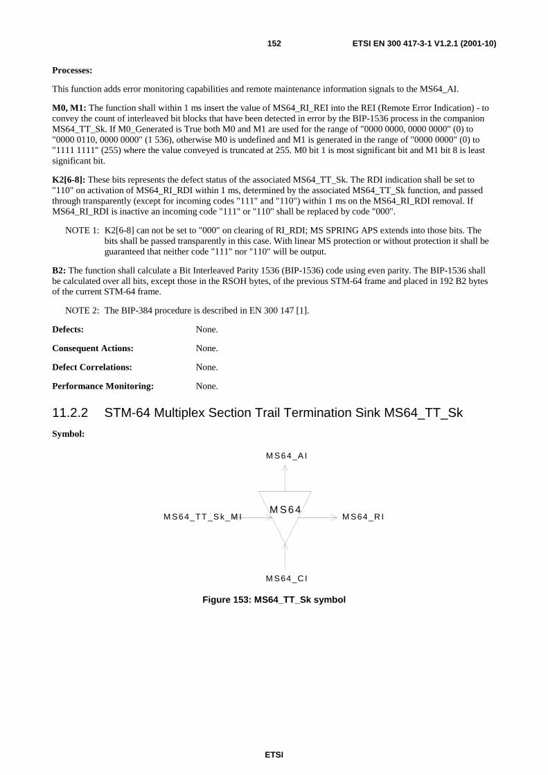
ETSI
ETSI EN 300 417-3-1 V1.2.1 (2001-10)152
Processes:
This function adds error monitoring capabilities and remote maintenance information signals to the MS64_AI.
M0, M1: The function shall within 1 ms insert the value of MS64_RI_REI into the REI (Remote Error Indication) - to convey the count of interleaved bit blocks that have been detected in error by the BIP-1536 process in the companion MS64_TT_Sk. If M0_Generated is True both M0 and M1 are used for the range of "0000 0000, 0000 0000" (0) to "0000 0110, 0000 0000" (1 536), otherwise M0 is undefined and M1 is generated in the range of "0000 0000" (0) to "1111 1111" (255) where the value conveyed is truncated at 255. M0 bit 1 is most significant bit and M1 bit 8 is least significant bit.
K2[6-8]: These bits represents the defect status of the associated MS64_TT_Sk. The RDI indication shall be set to "110" on activation of MS64_RI_RDI within 1 ms, determined by the associated MS64_TT_Sk function, and passed through transparently (except for incoming codes "111" and "110") within 1 ms on the MS64_RI_RDI removal. If MS64_RI_RDI is inactive an incoming code "111" or "110" shall be replaced by code "000".
NOTE 1: K2[6-8] can not be set to "000" on clearing of RI_RDI; MS SPRING APS extends into those bits. The bits shall be passed transparently in this case. With linear MS protection or without protection it shall be guaranteed that neither code "111" nor "110" will be output.
B2: The function shall calculate a Bit Interleaved Parity 1536 (BIP-1536) code using even parity. The BIP-1536 shall be calculated over all bits, except those in the RSOH bytes, of the previous STM-64 frame and placed in 192 B2 bytes of the current STM-64 frame.
NOTE 2: The BIP-384 procedure is described in EN 300 147 [1].
Defects: None.
Consequent Actions: None.
Defect Correlations: None.
Performance Monitoring: None.
11.2.2 STM-64 Multiplex Section Trail Termination Sink MS64_TT_Sk
Symbol:
M S6 4
M S64_A I
M S64_C I
M S64_TT_S k_M I M S64_R I
Figure 153: MS64_TT_Sk symbol
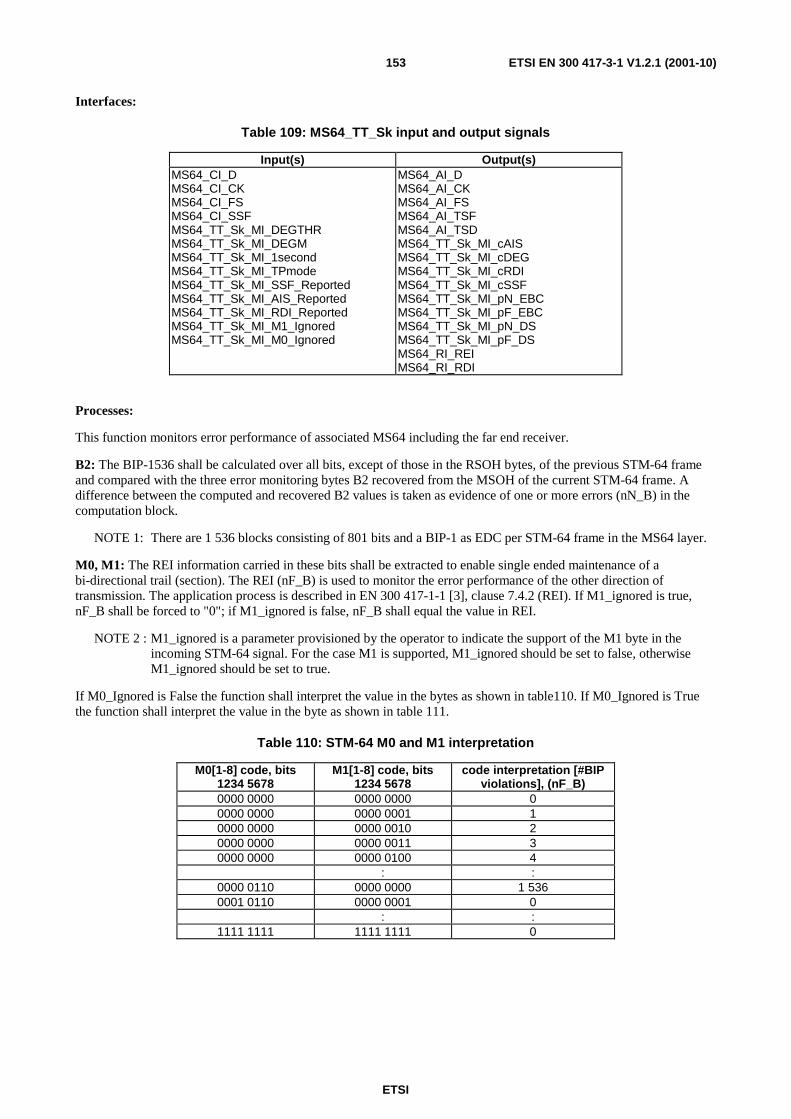
ETSI
ETSI EN 300 417-3-1 V1.2.1 (2001-10)153
Interfaces:
Table 109: MS64_TT_Sk input and output signals
Input(s) Output(s) MS64_CI_D MS64_CI_CK MS64_CI_FS MS64_CI_SSF MS64_TT_Sk_MI_DEGTHR MS64_TT_Sk_MI_DEGM MS64_TT_Sk_MI_1second MS64_TT_Sk_MI_TPmode MS64_TT_Sk_MI_SSF_Reported MS64_TT_Sk_MI_AIS_Reported MS64_TT_Sk_MI_RDI_Reported MS64_TT_Sk_MI_M1_Ignored MS64_TT_Sk_MI_M0_Ignored
MS64_AI_D MS64_AI_CK MS64_AI_FS MS64_AI_TSF MS64_AI_TSD MS64_TT_Sk_MI_cAIS MS64_TT_Sk_MI_cDEG MS64_TT_Sk_MI_cRDI MS64_TT_Sk_MI_cSSF MS64_TT_Sk_MI_pN_EBC MS64_TT_Sk_MI_pF_EBC MS64_TT_Sk_MI_pN_DS MS64_TT_Sk_MI_pF_DS MS64_RI_REI MS64_RI_RDI
Processes:
This function monitors error performance of associated MS64 including the far end receiver.
B2: The BIP-1536 shall be calculated over all bits, except of those in the RSOH bytes, of the previous STM-64 frame and compared with the three error monitoring bytes B2 recovered from the MSOH of the current STM-64 frame. A difference between the computed and recovered B2 values is taken as evidence of one or more errors (nN_B) in the computation block.
NOTE 1: There are 1 536 blocks consisting of 801 bits and a BIP-1 as EDC per STM-64 frame in the MS64 layer.
M0, M1: The REI information carried in these bits shall be extracted to enable single ended maintenance of a bi-directional trail (section). The REI (nF_B) is used to monitor the error performance of the other direction of transmission. The application process is described in EN 300 417-1-1 [3], clause 7.4.2 (REI). If M1_ignored is true, nF_B shall be forced to "0"; if M1_ignored is false, nF_B shall equal the value in REI.
NOTE 2 : M1_ignored is a parameter provisioned by the operator to indicate the support of the M1 byte in the incoming STM-64 signal. For the case M1 is supported, M1_ignored should be set to false, otherwise M1_ignored should be set to true.
If M0_Ignored is False the function shall interpret the value in the bytes as shown in table110. If M0_Ignored is True the function shall interpret the value in the byte as shown in table 111.
Table 110: STM-64 M0 and M1 interpretation
M0[1-8] code, bits 1234 5678
M1[1-8] code, bits 1234 5678
code interpretation [#BIP violations], (nF_B)
0000 0000 0000 0000 0 0000 0000 0000 0001 1 0000 0000 0000 0010 2 0000 0000 0000 0011 3 0000 0000 0000 0100 4
: : 0000 0110 0000 0000 1 536 0001 0110 0000 0001 0
: : 1111 1111 1111 1111 0
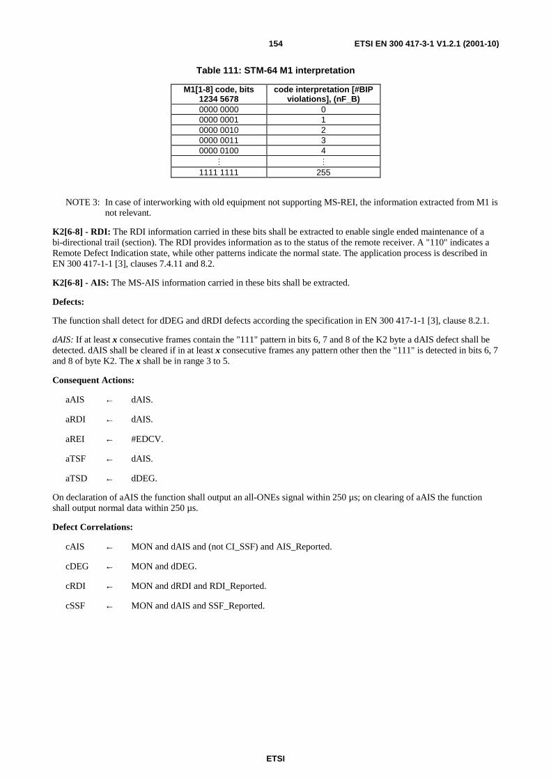
ETSI
ETSI EN 300 417-3-1 V1.2.1 (2001-10)154
Table 111: STM-64 M1 interpretation
M1[1-8] code, bits 1234 5678
code interpretation [#BIP violations], (nF_B)
0000 0000 0 0000 0001 1 0000 0010 2 0000 0011 3 0000 0100 4
M M 1111 1111 255
NOTE 3: In case of interworking with old equipment not supporting MS-REI, the information extracted from M1 is not relevant.
K2[6-8] - RDI: The RDI information carried in these bits shall be extracted to enable single ended maintenance of a bi-directional trail (section). The RDI provides information as to the status of the remote receiver. A "110" indicates a Remote Defect Indication state, while other patterns indicate the normal state. The application process is described in EN 300 417-1-1 [3], clauses 7.4.11 and 8.2.
K2[6-8] - AIS: The MS-AIS information carried in these bits shall be extracted.
Defects:
The function shall detect for dDEG and dRDI defects according the specification in EN 300 417-1-1 [3], clause 8.2.1.
dAIS: If at least x consecutive frames contain the "111" pattern in bits 6, 7 and 8 of the K2 byte a dAIS defect shall be detected. dAIS shall be cleared if in at least x consecutive frames any pattern other then the "111" is detected in bits 6, 7 and 8 of byte K2. The x shall be in range 3 to 5.
Consequent Actions:
aAIS ← dAIS.
aRDI ← dAIS.
aREI ← #EDCV.
aTSF ← dAIS.
aTSD ← dDEG.
On declaration of aAIS the function shall output an all-ONEs signal within 250 µs; on clearing of aAIS the function shall output normal data within 250 µs.
Defect Correlations:
cAIS ← MON and dAIS and (not CI_SSF) and AIS_Reported.
cDEG ← MON and dDEG.
cRDI ← MON and dRDI and RDI_Reported.
cSSF ← MON and dAIS and SSF_Reported.
ETSI
ETSI EN 300 417-3-1 V1.2.1 (2001-10)155
Performance monitoring:
The performance monitoring process shall be performed as specified in EN 300 417-1-1 [3], clause 8.2.4 through 8.2.7.
pN_DS ← aTSF or dEQ.
pF_DS ← dRDI.
pN_EBC ← Σ nN_B.
pF_EBC ← Σ nF_B.
11.3 STM-64 Multiplex Section Adaptation functions
11.3.1 STM-64 Multiplex Section to S4 Layer Adaptation Source MS64/S4_A_So/(D,C,B,0)
Symbol:
M S 64 /S 4 -N
S4_CI
M S64_AI
M S64/S4_A_So_M I STM 64_TI
N=(1,1,1,0) .. (4,4,4,0)
Figure 154: MS64/S4_A_So symbol
Interfaces:
Table 112: MS64/S4_A_So input and output signals
Input(s) Output(s) S4_CI_D S4_CI_CK S4_CI_FS S4_CI_SSF STM64_TI_CK STM64_TI_FS MS64/S4_A_So_MI_Active
MS64_AI_D MS64_AI_CK MS64_AI_FS MS64/S4_A_So_MI_pPJE+ MS64/S4_A_So_MI_pPJE-
Processes:
This function provides frequency justification and bitrate adaptation for a VC-4 signal, represented by a nominally (261 x 9 x 64) = 150 336 kbit/s information stream and the related frame phase with a frequency accuracy within ± 4,6 ppm, to be multiplexed into a STM-64 signal at the AU tributary location indicated by (D,C,B,0), where D designates the AUG-16 number (1 to 4), C designates the AUG-4 number (1 to 4) and B designates the AUG-1 number (1 to 4). The function can be activated / deactivated when multiple payload adaptation functions are connected to the access point.
NOTE 1: Degraded performance may be observed when interworking with SONET equipment having a ± 20 ppm network element clock source.
The frame phase of the VC-4 is coded in the related AU-4 pointer. Frequency justification, if required, is performed by pointer adjustments. The accuracy of this coding process is specified below. See EN 300 417-4-1 [4], annex A.
Frequency justification and bitrate adaptation: The function shall provide for an elastic store (buffer) process. The data and frame start signals shall be written into the buffer under control of the associated input clock. The data and frame start signals shall be read out of the buffer under control of the STM-64 clock, frame position, and justification decision.
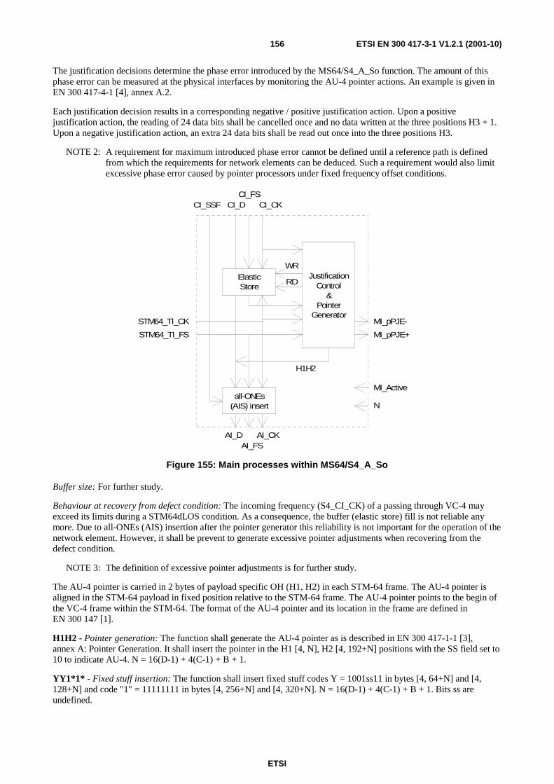
ETSI
ETSI EN 300 417-3-1 V1.2.1 (2001-10)156
The justification decisions determine the phase error introduced by the MS64/S4_A_So function. The amount of this phase error can be measured at the physical interfaces by monitoring the AU-4 pointer actions. An example is given in EN 300 417-4-1 [4], annex A.2.
Each justification decision results in a corresponding negative / positive justification action. Upon a positive justification action, the reading of 24 data bits shall be cancelled once and no data written at the three positions H3 + 1. Upon a negative justification action, an extra 24 data bits shall be read out once into the three positions H3.
NOTE 2: A requirement for maximum introduced phase error cannot be defined until a reference path is defined from which the requirements for network elements can be deduced. Such a requirement would also limit excessive phase error caused by pointer processors under fixed frequency offset conditions.
ElasticStore
JustificationControl
&Pointer
Generator
STM64_TI_FS
STM64_TI_CK
WR
RD
all-ONEs(AIS) insert
CI_SSF CI_DCI_FS
CI_CK
AI_DAI_FS
AI_CK
H1H2
MI_pPJE-
MI_pPJE+
MI_Active
N
Figure 155: Main processes within MS64/S4_A_So
Buffer size: For further study.
Behaviour at recovery from defect condition: The incoming frequency (S4_CI_CK) of a passing through VC-4 may exceed its limits during a STM64dLOS condition. As a consequence, the buffer (elastic store) fill is not reliable any more. Due to all-ONEs (AIS) insertion after the pointer generator this reliability is not important for the operation of the network element. However, it shall be prevent to generate excessive pointer adjustments when recovering from the defect condition.
NOTE 3: The definition of excessive pointer adjustments is for further study.
The AU-4 pointer is carried in 2 bytes of payload specific OH (H1, H2) in each STM-64 frame. The AU-4 pointer is aligned in the STM-64 payload in fixed position relative to the STM-64 frame. The AU-4 pointer points to the begin of the VC-4 frame within the STM-64. The format of the AU-4 pointer and its location in the frame are defined in EN 300 147 [1].
H1H2 - Pointer generation: The function shall generate the AU-4 pointer as is described in EN 300 417-1-1 [3], annex A: Pointer Generation. It shall insert the pointer in the H1 [4, N], H2 [4, 192+N] positions with the SS field set to 10 to indicate AU-4. N = 16(D-1) + 4(C-1) + B + 1.
YY1*1* - Fixed stuff insertion: The function shall insert fixed stuff codes Y = 1001ss11 in bytes [4, 64+N] and [4, 128+N] and code "1" = 11111111 in bytes [4, 256+N] and [4, 320+N]. N = 16(D-1) + 4(C-1) + B + 1. Bits ss are undefined.
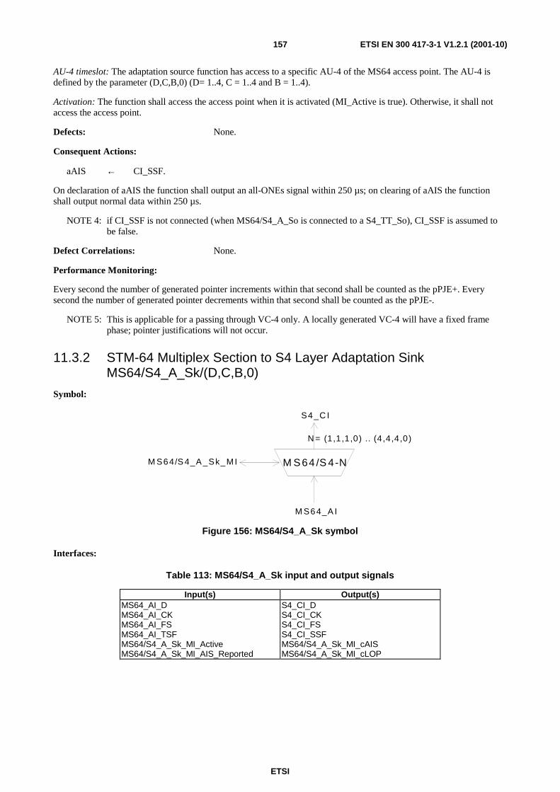
ETSI
ETSI EN 300 417-3-1 V1.2.1 (2001-10)157
AU-4 timeslot: The adaptation source function has access to a specific AU-4 of the MS64 access point. The AU-4 is defined by the parameter (D,C,B,0) (D= 1..4, C = 1..4 and B = 1..4).
Activation: The function shall access the access point when it is activated (MI_Active is true). Otherwise, it shall not access the access point.
Defects: None.
Consequent Actions:
aAIS ← CI_SSF.
On declaration of aAIS the function shall output an all-ONEs signal within 250 µs; on clearing of aAIS the function shall output normal data within 250 µs.
NOTE 4: if CI_SSF is not connected (when MS64/S4_A_So is connected to a S4_TT_So), CI_SSF is assumed to be false.
Defect Correlations: None.
Performance Monitoring:
Every second the number of generated pointer increments within that second shall be counted as the pPJE+. Every second the number of generated pointer decrements within that second shall be counted as the pPJE-.
NOTE 5: This is applicable for a passing through VC-4 only. A locally generated VC-4 will have a fixed frame phase; pointer justifications will not occur.
11.3.2 STM-64 Multiplex Section to S4 Layer Adaptation Sink MS64/S4_A_Sk/(D,C,B,0)
Symbol:
M S64 /S 4-N
S4_C I
M S64_A I
M S64/S 4_A _Sk_M I
N = (1,1,1,0) .. (4,4,4,0)
Figure 156: MS64/S4_A_Sk symbol
Interfaces:
Table 113: MS64/S4_A_Sk input and output signals
Input(s) Output(s) MS64_AI_D MS64_AI_CK MS64_AI_FS MS64_AI_TSF MS64/S4_A_Sk_MI_Active MS64/S4_A_Sk_MI_AIS_Reported
S4_CI_D S4_CI_CK S4_CI_FS S4_CI_SSF MS64/S4_A_Sk_MI_cAIS MS64/S4_A_Sk_MI_cLOP
ETSI
ETSI EN 300 417-3-1 V1.2.1 (2001-10)158
Processes:
This function recovers the VC-4 data with frame phase information from the STM-64 as defined in EN 300 147 [1]. The VC-4 is extracted from the AU tributary location indicated by (D,C,B,0), where D designates the AUG-16 number (1 to 4), C designates the AUG-4 number (1 to 4) and B designates the AUG-1 number (1 to 4). The function can be activated / deactivated when multiple payload adaptation functions are connected to the access point.
H1H2 - AU-4 pointer interpretation: An AU-4 pointer consists of 2 bytes, [4, N] and [4, 192+N]. The function shall perform AU-4 pointer interpretation according to annex B of EN 300 417-1-1 [3] to recover the VC-4 frame phase within the STM-64. The process shall maintain its current phase on detection of an invalid pointer and searches in parallel for a new phase. N = 16(D-1) + 4(C-1) + B + 1.
YY1*1*: The bytes [4, 64+N], [4, 128+N], [4, 256+N], and [4, 320+N] contain fixed stuff, of a specified value, ignored by the AU-4 pointer interpreter. N = 16(D-1) + 4(C-1) + B + 1.
AU-4 timeslot: The adaptation sink function has access to a specific AU-4 of the MS64 access point. The AU-4 is defined by the parameter (D,C,B,0) (D= 1..4, C = 1..4 and B = 1..4).
Activation: The function shall perform the operation specified above when it is activated (MI_Active is true). Otherwise, it shall transmit the all-ONEs signal at its output (CI_D) and not report its status via its management point.
Defects:
dAIS: The dAIS defect shall be detected if the pointer interpreter is in the AIS_state (see EN 300 417-1-1 [3], annex B). The dAIS defect shall be cleared if the pointer interpreter is not in the AIS_state.
dLOP: The dLOP defect shall be detected if the pointer interpreter is in the LOP_state (see EN 300 417-1-1 [3], annex B). The dLOP defect shall be cleared if the pointer interpreter is not in the LOP_state.
Consequent Actions:
aAIS ← dAIS or dLOP.
aSSF ← dAIS or dLOP.
On declaration of aAIS the function shall output an all-ONEs (AIS) signal within 250 µs; on clearing of aAIS the function shall output the recovered data within 250 µs.
Defect Correlations:
cAIS ← dAIS and (not AI_TSF) and AIS_Reported.
cLOP ← dLOP.
Performance Monitoring: None.
11.3.3 STM-64 Multiplex Section to S4-4c Layer Adaptation Source MS64/S4-4c_A_So/(D,C,0,0)
Symbol:
MS64/S4-4c-N
S4-4c_CI
MS64_AI
MS64/S4-4c_A_So_MI STM64_TI
N=(1,1,0,0) .. (4,4,0,0)
Figure 157: MS4/S4-4c_A_So symbol
ETSI
ETSI EN 300 417-3-1 V1.2.1 (2001-10)159
Interfaces:
Table 114: MS64/S4-4c_A_So input and output signals
Input(s) Output(s) S4-4c_CI_D S4-4c_CI_CK S4-4c_CI_FS S4-4c_CI_SSF STM64_TI_CK STM64_TI_FS MS64/S4-4c_A_So_MI_Active
MS64_AI_D MS64_AI_CK MS64_AI_FS MS64/S4-4c_A_So_MI_pPJE+ MS64/S4-4c_A_So_MI_pPJE-
Processes:
This function provides frequency justification and bitrate adaptation for a VC-4-4c signal, represented by a nominally (4 x 261 x 9 x 64) = 601 344 kbit/s information stream and the related frame phase with a frequency accuracy within ± 4,6 ppm, to be multiplexed into a STM-64 signal at the AU-4-4c tributary location indicated by (D,C,0,0), where D designates the AUG-16 number (1 to 4) and C designates the AUG-4 number (1 to 4). The function can be activated / deactivated when multiple payload adaptation functions are connected to the access point.
NOTE 1: Degraded performance may be observed when interworking with SONET equipment having a ± 20 ppm network element clock source.
The frame phase of the VC-4-4c is coded in the related AU-4-4c pointer. Frequency justification, if required, is performed by pointer adjustments. The accuracy of this coding process is specified below. See EN 300 417-4-1 [4], annex A.
Frequency justification and bitrate adaptation: The function shall provide for an elastic store (buffer) process. The data and frame start signals shall be written into the buffer under control of the associated input clock. The data and frame start signals shall be read out of the buffer under control of the STM-64 clock, frame position, and justification decision.
The justification decisions determine the phase error introduced by the MS64/S4-4c_A_So function. The amount of this phase error can be measured at the physical interfaces by monitoring the AU-4-4c pointer actions. An example is given in EN 30 417-4-1 [4], clause A.2.
Each justification decision results in a corresponding negative / positive justification action. Upon a positive justification action, the reading of 96 data bits shall be cancelled once and no data written at the twelve positions H3 + 1. Upon a negative justification action, an extra 96 data bits shall be read out once into the twelve positions H3.
NOTE 2: A requirement for maximum introduced phase error cannot be defined until a reference path is defined from which the requirements for network elements can be deduced. Such a requirement would also limit excessive phase error caused by pointer processors under fixed frequency offset conditions.
Buffer size: For further study.
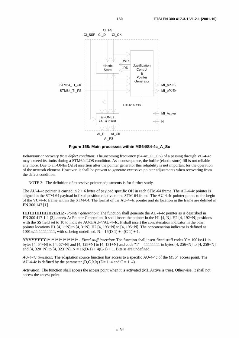
ETSI
ETSI EN 300 417-3-1 V1.2.1 (2001-10)160
ElasticStore
JustificationControl
&Pointer
Generator
STM64_TI_FS
STM64_TI_CK
WR
RD
all-ONEs(AIS) insert
CI_SSF CI_DCI_FS
CI_CK
AI_DAI_FS
AI_CK
H1H2 & CIs
MI_pPJE-
MI_pPJE+
MI_Active
N
Figure 158: Main processes within MS64/S4-4c_A_So
Behaviour at recovery from defect condition: The incoming frequency (S4-4c_CI_CK) of a passing through VC-4-4c may exceed its limits during a STM64dLOS condition. As a consequence, the buffer (elastic store) fill is not reliable any more. Due to all-ONEs (AIS) insertion after the pointer generator this reliability is not important for the operation of the network element. However, it shall be prevent to generate excessive pointer adjustments when recovering from the defect condition.
NOTE 3: The definition of excessive pointer adjustments is for further study.
The AU-4-4c pointer is carried in 2 + 6 bytes of payload specific OH in each STM-64 frame. The AU-4-4c pointer is aligned in the STM-64 payload in fixed position relative to the STM-64 frame. The AU-4-4c pointer points to the begin of the VC-4-4c frame within the STM-64. The format of the AU-4-4c pointer and its location in the frame are defined in EN 300 147 [1].
H1H1H1H1H2H2H2H2 - Pointer generation: The function shall generate the AU-4-4c pointer as is described in EN 300 417-1-1 [3], annex A: Pointer Generation. It shall insert the pointer in the H1 [4, N], H2 [4, 192+N] positions with the SS field set to 10 to indicate AU-3/AU-4/AU-4-4c. It shall insert the concatenation indicator in the other pointer locations H1 [4, 1+N] to [4, 3+N], H2 [4, 193+N] to [4, 195+N]. The concatenation indicator is defined as 1001ss11 11111111, with ss being undefined. N = 16(D-1) + 4(C-1) + 1.
YYYYYYYY1*1*1*1*1*1*1*1* - Fixed stuff insertion: The function shall insert fixed stuff codes Y = 1001ss11 in bytes [4, 64+N] to [4, 67+N] and [4, 128+N] to [4, 131+N] and code "1" = 11111111 in bytes [4, 256+N] to [4, 259+N] and [4, 320+N] to [4, 323+N], N = 16(D-1) + 4(C-1) + 1. Bits ss are undefined.
AU-4-4c timeslots: The adaptation source function has access to a specific AU-4-4c of the MS64 access point. The AU-4-4c is defined by the parameter (D,C,0,0) (D= 1..4 and C = 1..4).
Activation: The function shall access the access point when it is activated (MI_Active is true). Otherwise, it shall not access the access point.
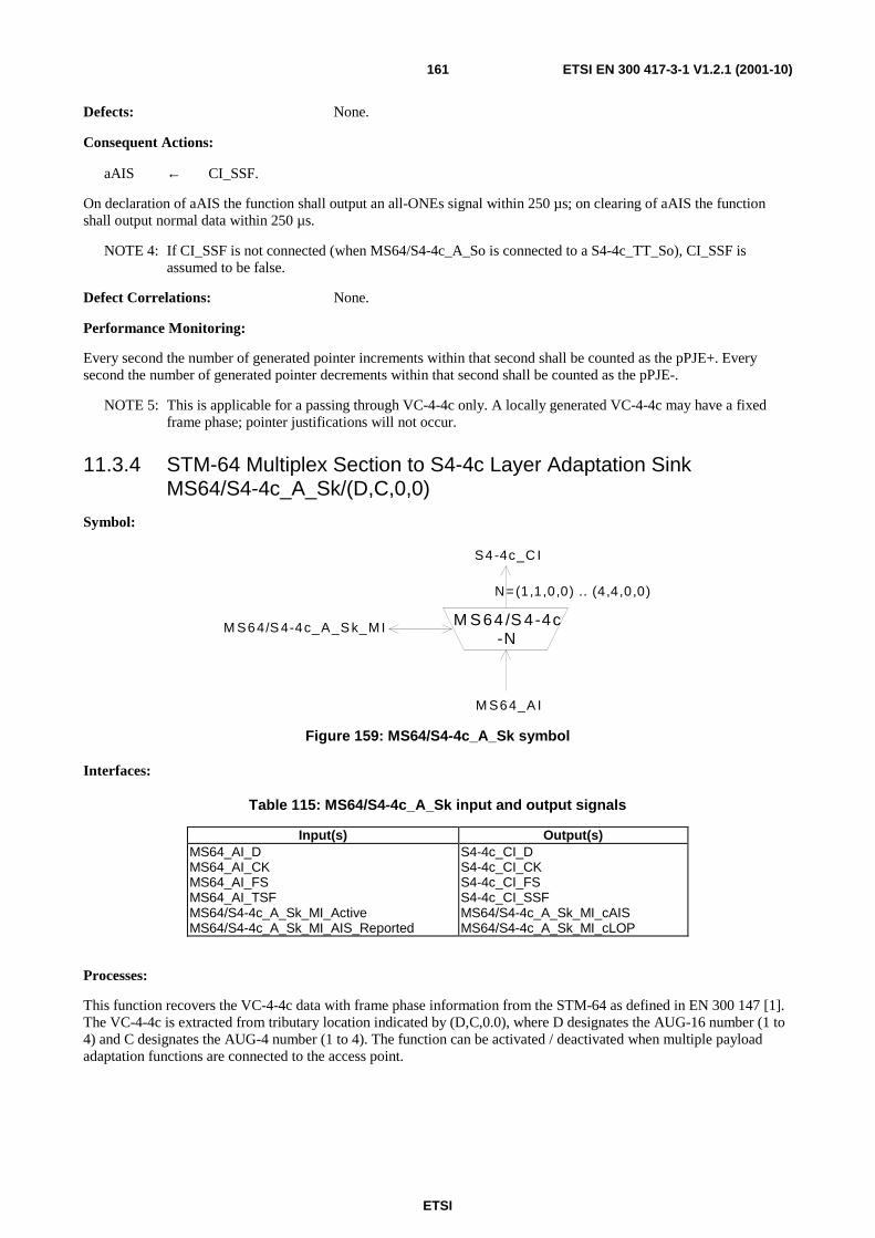
ETSI
ETSI EN 300 417-3-1 V1.2.1 (2001-10)161
Defects: None.
Consequent Actions:
aAIS ← CI_SSF.
On declaration of aAIS the function shall output an all-ONEs signal within 250 µs; on clearing of aAIS the function shall output normal data within 250 µs.
NOTE 4: If CI_SSF is not connected (when MS64/S4-4c_A_So is connected to a S4-4c_TT_So), CI_SSF is assumed to be false.
Defect Correlations: None.
Performance Monitoring:
Every second the number of generated pointer increments within that second shall be counted as the pPJE+. Every second the number of generated pointer decrements within that second shall be counted as the pPJE-.
NOTE 5: This is applicable for a passing through VC-4-4c only. A locally generated VC-4-4c may have a fixed frame phase; pointer justifications will not occur.
11.3.4 STM-64 Multiplex Section to S4-4c Layer Adaptation Sink MS64/S4-4c_A_Sk/(D,C,0,0)
Symbol:
M S64 /S 4-4c-N
S4-4c_C I
M S64_A I
M S64/S 4-4c_A_S k_M I
N=(1,1,0,0) .. (4,4,0,0)
Figure 159: MS64/S4-4c_A_Sk symbol
Interfaces:
Table 115: MS64/S4-4c_A_Sk input and output signals
Input(s) Output(s) MS64_AI_D MS64_AI_CK MS64_AI_FS MS64_AI_TSF MS64/S4-4c_A_Sk_MI_Active MS64/S4-4c_A_Sk_MI_AIS_Reported
S4-4c_CI_D S4-4c_CI_CK S4-4c_CI_FS S4-4c_CI_SSF MS64/S4-4c_A_Sk_MI_cAIS MS64/S4-4c_A_Sk_MI_cLOP
Processes:
This function recovers the VC-4-4c data with frame phase information from the STM-64 as defined in EN 300 147 [1]. The VC-4-4c is extracted from tributary location indicated by (D,C,0.0), where D designates the AUG-16 number (1 to 4) and C designates the AUG-4 number (1 to 4). The function can be activated / deactivated when multiple payload adaptation functions are connected to the access point.
ETSI
ETSI EN 300 417-3-1 V1.2.1 (2001-10)162
H1H1H1H1H2H2H2H2 - AU-4-4c pointer interpretation: An AU-4-4c pointer consists of 2 bytes, [4, N] and [4, 192+N]. There will be 3 concatenation indicators, each 2 bytes long, in [4, 1+N]/[4, 193+N], [4, 2+N]/[4, 194+N], and [4, 3+N]/[4, 195+N]. The function shall perform AU-4-4c pointer interpretation according to annex B of EN 300 417-1-1 [3] to recover the VC-4-4c frame phase within the STM-64. The process shall maintain its current phase on detection of an invalid pointer and searches in parallel for a new phase. N = 16(D-1) + 4(C-1) + 1.
YYYYYYYY1*1*1*1*1*1*1*1*: The bytes [4, 64+N] to [4, 67+N], [4, 128+N] to [4, 131+N], [4, 256+N] to [4, 259+N] and [4, 320+N] to [4, 323+N] contain fixed stuff, of a specified value, ignored by the AU-4-4c pointer interpreter. N = 16(D-1) + 4(C-1) + 1.
AU-4-4c timeslots: The adaptation source function has access to a specific AU-4-4c of the MS64 access point. The AU-4-4c is defined by the parameter (D,C,0,0) (D= 1..4 and C = 1..4).
Activation: The function shall perform the operation specified above when it is activated (MI_Active is true). Otherwise, it shall transmit the all-ONEs signal at its output (CI_D) and not report its status via its management point.
Defects:
dAIS: The dAIS defect shall be detected if the pointer interpreter is in the AISX_state (see EN 300 417-1-1 [3], annex B). The dAIS defect shall be cleared if the pointer interpreter is not in the AISX_state.
dLOP: The dLOP defect shall be detected if the pointer interpreter is in the LOPX_state (see EN 300 417-1-1 [3], annex B). The dLOP defect shall be cleared if the pointer interpreter is not in the LOPX_state.
Consequent Actions:
aAIS ← dAIS or dLOP.
aSSF ← dAIS or dLOP.
On declaration of aAIS the function shall output an all-ONEs (AIS) signal within 250 µs; on clearing of aAIS the function shall output the recovered data within 250 µs.
Defect Correlations:
cAIS ← dAIS and (not aTSF) and AIS_Reported.
cLOP ← dLOP.
Performance Monitoring: None.
11.3.5 STM-64 Multiplex Section to S4-16c Layer Adaptation Source MS64/S4-16c_A_So/(D,0,0,0)
Symbol:
M S6 4/S 4-16c-N
S4-16c_C I
M S64_A I
M S64/S4-16c_A _So_M I STM 64_TI
N=(1,0,0,0) .. (4,0,0,0)
Figure 160: MS64/S4-16c_A_So symbol

ETSI
ETSI EN 300 417-3-1 V1.2.1 (2001-10)163
Interfaces:
Table 116: MS64/S4-16c_A_So input and output signals
Input(s) Output(s) S4-16c_CI_D S4-16c_CI_CK S4-16c_CI_FS S4-16c_CI_SSF STM64_TI_CK STM64_TI_FS MS64/S4-16c_A_So_MI_Active
MS64_AI_D MS64_AI_CK MS64_AI_FS MS64/S4-16c_A_So_MI_pPJE+ MS64/S4-16c_A_So_MI_pPJE-
Processes:
This function provides frequency justification and bitrate adaptation for a VC-4-16c signal, represented by a nominally (16 x 261 x 9 x 64) = 2 405 376 kbit/s information stream and the related frame phase with a frequency accuracy within ± 4,6 ppm, to be multiplexed into a STM-64 signal at the AU-4-16c tributary location indicated by (D,0,0,0), where D designates the AUG-16 number (1 to 4). The function can be activated / deactivated when multiple payload adaptation functions are connected to the access point.
NOTE 1: Degraded performance may be observed when interworking with SONET equipment having a ± 20 ppm network element clock source.
The frame phase of the VC-4-16c is coded in the related AU-4-16c pointer. Frequency justification, if required, is performed by pointer adjustments. The accuracy of this coding process is specified below. See EN 300 417-4-1 [4], annex A.
Frequency justification and bitrate adaptation: The function shall provide for an elastic store (buffer) process. The data and frame start signals shall be written into the buffer under control of the associated input clock. The data and frame start signals shall be read out of the buffer under control of the STM-64 clock, frame position, and justification decision.
The justification decisions determine the phase error introduced by the MS64/S4-16c_A_So function. The amount of this phase error can be measured at the physical interfaces by monitoring the AU-4-16c pointer actions. An example is given in EN 300 417-4-1 [4], clause A.2.
Each justification decision results in a corresponding negative / positive justification action. Upon a positive justification action, the reading of 384 data bits shall be cancelled once and no data written at the 48 positions H3 + 1. Upon a negative justification action, an extra 384 data bits shall be read out once into the 48 positions H3.
NOTE 2: A requirement for maximum introduced phase error cannot be defined until a reference path is defined from which the requirements for network elements can be deduced. Such a requirement would also limit excessive phase error caused by pointer processors under fixed frequency offset conditions.
Buffer size: For further study.
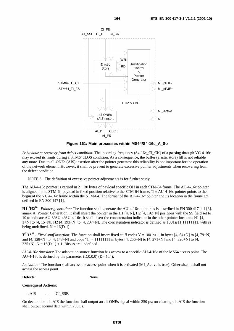
ETSI
ETSI EN 300 417-3-1 V1.2.1 (2001-10)164
ElasticStore
JustificationControl
&Pointer
Generator
STM64_TI_FS
STM64_TI_CK
WR
RD
all-ONEs(AIS) insert
CI_SSF CI_DCI_FS
CI_CK
AI_DAI_FS
AI_CK
H1H2 & CIs
MI_pPJE-
MI_pPJE+
MI_Active
N
Figure 161: Main processes within MS64/S4-16c_A_So
Behaviour at recovery from defect condition: The incoming frequency (S4-16c_CI_CK) of a passing through VC-4-16c may exceed its limits during a STM64dLOS condition. As a consequence, the buffer (elastic store) fill is not reliable any more. Due to all-ONEs (AIS) insertion after the pointer generator this reliability is not important for the operation of the network element. However, it shall be prevent to generate excessive pointer adjustments when recovering from the defect condition.
NOTE 3: The definition of excessive pointer adjustments is for further study.
The AU-4-16c pointer is carried in 2 + 30 bytes of payload specific OH in each STM-64 frame. The AU-4-16c pointer is aligned in the STM-64 payload in fixed position relative to the STM-64 frame. The AU-4-16c pointer points to the begin of the VC-4-16c frame within the STM-64. The format of the AU-4-16c pointer and its location in the frame are defined in EN 300 147 [1].
H116H216 - Pointer generation: The function shall generate the AU-4-16c pointer as is described in EN 300 417-1-1 [3], annex A: Pointer Generation. It shall insert the pointer in the H1 [4, N], H2 [4, 192+N] positions with the SS field set to 10 to indicate AU-3/AU-4/AU-4-16c. It shall insert the concatenation indicator in the other pointer locations H1 [4, 1+N] to [4, 15+N], H2 [4, 193+N] to [4, 207+N]. The concatenation indicator is defined as 1001ss11 11111111, with ss being undefined. N = 16(D-1).
Y321*32 - Fixed stuff insertion: The function shall insert fixed stuff codes Y = 1001ss11 in bytes [4, 64+N] to [4, 79+N] and [4, 128+N] to [4, 143+N] and code "1" = 11111111 in bytes [4, 256+N] to [4, 271+N] and [4, 320+N] to [4, 335+N], N = 16(D-1) + 1. Bits ss are undefined.
AU-4-16c timeslots: The adaptation source function has access to a specific AU-4-16c of the MS64 access point. The AU-4-16c is defined by the parameter (D,0,0,0) (D= 1..4).
Activation: The function shall access the access point when it is activated (MI_Active is true). Otherwise, it shall not access the access point.
Defects: None.
Consequent Actions:
aAIS ← CI_SSF.
On declaration of aAIS the function shall output an all-ONEs signal within 250 µs; on clearing of aAIS the function shall output normal data within 250 µs.
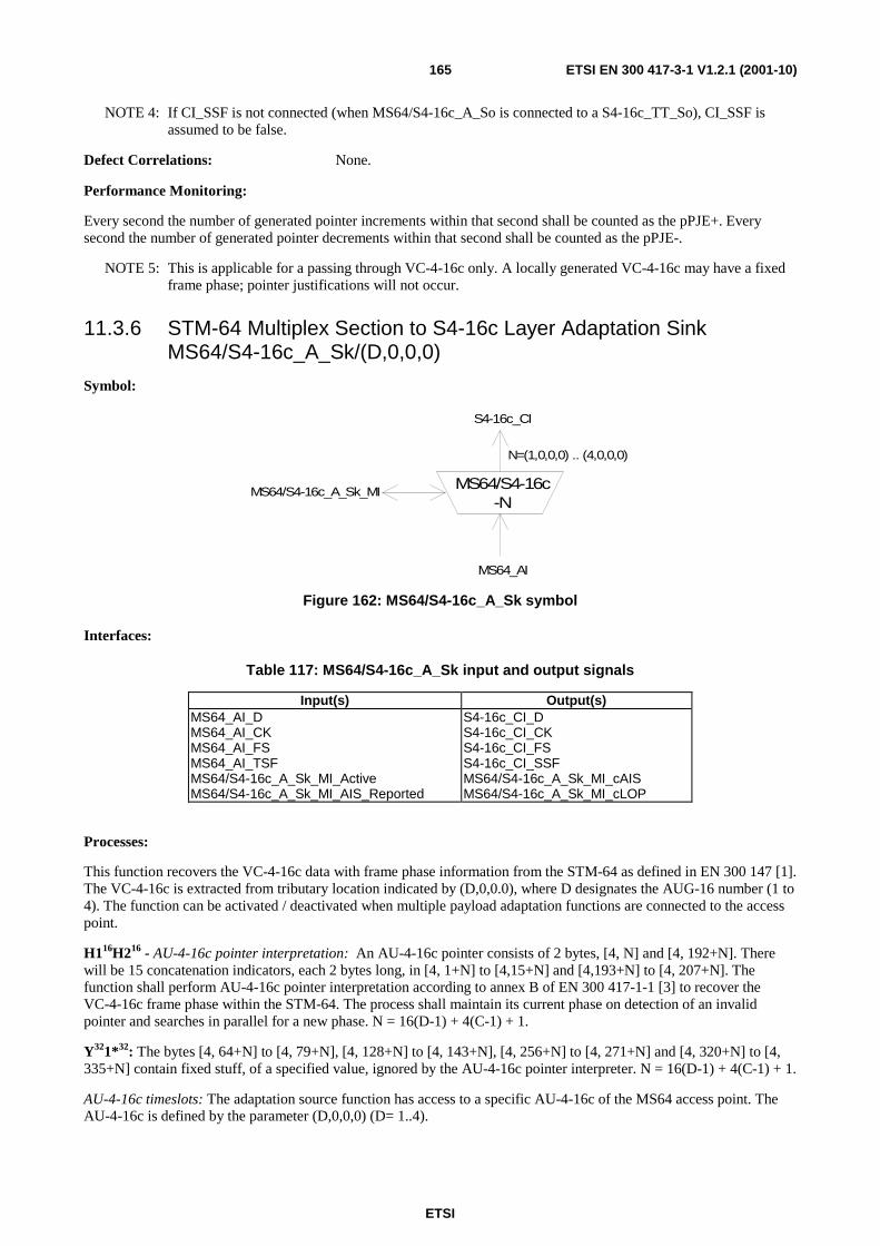
ETSI
ETSI EN 300 417-3-1 V1.2.1 (2001-10)165
NOTE 4: If CI_SSF is not connected (when MS64/S4-16c_A_So is connected to a S4-16c_TT_So), CI_SSF is assumed to be false.
Defect Correlations: None.
Performance Monitoring:
Every second the number of generated pointer increments within that second shall be counted as the pPJE+. Every second the number of generated pointer decrements within that second shall be counted as the pPJE-.
NOTE 5: This is applicable for a passing through VC-4-16c only. A locally generated VC-4-16c may have a fixed frame phase; pointer justifications will not occur.
11.3.6 STM-64 Multiplex Section to S4-16c Layer Adaptation Sink MS64/S4-16c_A_Sk/(D,0,0,0)
Symbol:
MS64/S4-16c-N
S4-16c_CI
MS64_AI
MS64/S4-16c_A_Sk_MI
N=(1,0,0,0) .. (4,0,0,0)
Figure 162: MS64/S4-16c_A_Sk symbol
Interfaces:
Table 117: MS64/S4-16c_A_Sk input and output signals
Input(s) Output(s) MS64_AI_D MS64_AI_CK MS64_AI_FS MS64_AI_TSF MS64/S4-16c_A_Sk_MI_Active MS64/S4-16c_A_Sk_MI_AIS_Reported
S4-16c_CI_D S4-16c_CI_CK S4-16c_CI_FS S4-16c_CI_SSF MS64/S4-16c_A_Sk_MI_cAIS MS64/S4-16c_A_Sk_MI_cLOP
Processes:
This function recovers the VC-4-16c data with frame phase information from the STM-64 as defined in EN 300 147 [1]. The VC-4-16c is extracted from tributary location indicated by (D,0,0.0), where D designates the AUG-16 number (1 to 4). The function can be activated / deactivated when multiple payload adaptation functions are connected to the access point.
H116H216 - AU-4-16c pointer interpretation: An AU-4-16c pointer consists of 2 bytes, [4, N] and [4, 192+N]. There will be 15 concatenation indicators, each 2 bytes long, in [4, 1+N] to [4,15+N] and [4,193+N] to [4, 207+N]. The function shall perform AU-4-16c pointer interpretation according to annex B of EN 300 417-1-1 [3] to recover the VC-4-16c frame phase within the STM-64. The process shall maintain its current phase on detection of an invalid pointer and searches in parallel for a new phase. N = 16(D-1) + 4(C-1) + 1.
Y321*32: The bytes [4, 64+N] to [4, 79+N], [4, 128+N] to [4, 143+N], [4, 256+N] to [4, 271+N] and [4, 320+N] to [4, 335+N] contain fixed stuff, of a specified value, ignored by the AU-4-16c pointer interpreter. N = 16(D-1) + 4(C-1) + 1.
AU-4-16c timeslots: The adaptation source function has access to a specific AU-4-16c of the MS64 access point. The AU-4-16c is defined by the parameter (D,0,0,0) (D= 1..4).
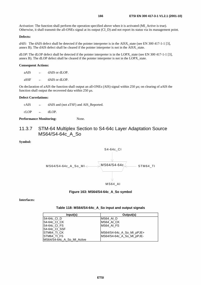
ETSI
ETSI EN 300 417-3-1 V1.2.1 (2001-10)166
Activation: The function shall perform the operation specified above when it is activated (MI_Active is true). Otherwise, it shall transmit the all-ONEs signal at its output (CI_D) and not report its status via its management point.
Defects:
dAIS: The dAIS defect shall be detected if the pointer interpreter is in the AISX_state (see EN 300 417-1-1 [3], annex B). The dAIS defect shall be cleared if the pointer interpreter is not in the AISX_state.
dLOP: The dLOP defect shall be detected if the pointer interpreter is in the LOPX_state (see EN 300 417-1-1 [3], annex B). The dLOP defect shall be cleared if the pointer interpreter is not in the LOPX_state.
Consequent Actions:
aAIS ← dAIS or dLOP.
aSSF ← dAIS or dLOP.
On declaration of aAIS the function shall output an all-ONEs (AIS) signal within 250 µs; on clearing of aAIS the function shall output the recovered data within 250 µs.
Defect Correlations:
cAIS ← dAIS and (not aTSF) and AIS_Reported.
cLOP ← dLOP.
Performance Monitoring: None.
11.3.7 STM-64 Multiplex Section to S4-64c Layer Adaptation Source MS64/S4-64c_A_So
Symbol:
MS64/S4-64c
S4-64c_CI
M S64_AI
M S64/S4-64c_A_So_M I STM 64_TI
Figure 163: MS64/S4-64c_A_So symbol
Interfaces:
Table 118: MS64/S4-64c_A_So input and output signals
Input(s) Output(s) S4-64c_CI_D S4-64c_CI_CK S4-64c_CI_FS S4-64c_CI_SSF STM64_TI_CK STM64_TI_FS MS64/S4-64c_A_So_MI_Active
MS64_AI_D MS64_AI_CK MS64_AI_FS MS64/S4-64c_A_So_MI_pPJE+ MS64/S4-64c_A_So_MI_pPJE-
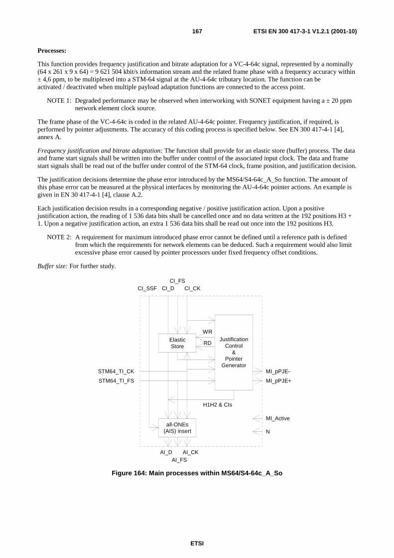
ETSI
ETSI EN 300 417-3-1 V1.2.1 (2001-10)167
Processes:
This function provides frequency justification and bitrate adaptation for a VC-4-64c signal, represented by a nominally (64 x 261 x 9 x 64) = 9 621 504 kbit/s information stream and the related frame phase with a frequency accuracy within ± 4,6 ppm, to be multiplexed into a STM-64 signal at the AU-4-64c tributary location. The function can be activated / deactivated when multiple payload adaptation functions are connected to the access point.
NOTE 1: Degraded performance may be observed when interworking with SONET equipment having a ± 20 ppm network element clock source.
The frame phase of the VC-4-64c is coded in the related AU-4-64c pointer. Frequency justification, if required, is performed by pointer adjustments. The accuracy of this coding process is specified below. See EN 300 417-4-1 [4], annex A.
Frequency justification and bitrate adaptation: The function shall provide for an elastic store (buffer) process. The data and frame start signals shall be written into the buffer under control of the associated input clock. The data and frame start signals shall be read out of the buffer under control of the STM-64 clock, frame position, and justification decision.
The justification decisions determine the phase error introduced by the MS64/S4-64c_A_So function. The amount of this phase error can be measured at the physical interfaces by monitoring the AU-4-64c pointer actions. An example is given in EN 30 417-4-1 [4], clause A.2.
Each justification decision results in a corresponding negative / positive justification action. Upon a positive justification action, the reading of 1 536 data bits shall be cancelled once and no data written at the 192 positions H3 + 1. Upon a negative justification action, an extra 1 536 data bits shall be read out once into the 192 positions H3.
NOTE 2: A requirement for maximum introduced phase error cannot be defined until a reference path is defined from which the requirements for network elements can be deduced. Such a requirement would also limit excessive phase error caused by pointer processors under fixed frequency offset conditions.
Buffer size: For further study.
ElasticStore
JustificationControl
&Pointer
Generator
STM64_TI_FS
STM64_TI_CK
WR
RD
all-ONEs(AIS) insert
CI_SSF CI_DCI_FS
CI_CK
AI_DAI_FS
AI_CK
H1H2 & CIs
MI_pPJE-
MI_pPJE+
MI_Active
N
Figure 164: Main processes within MS64/S4-64c_A_So
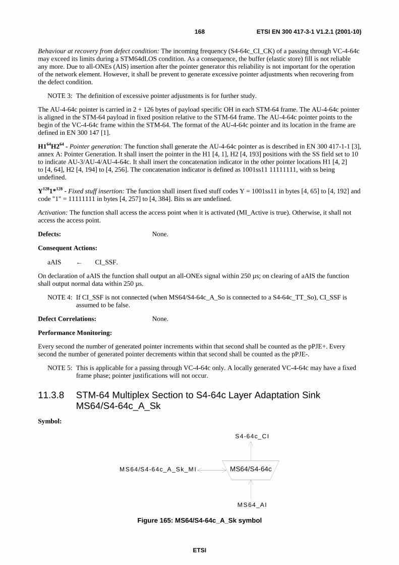
ETSI
ETSI EN 300 417-3-1 V1.2.1 (2001-10)168
Behaviour at recovery from defect condition: The incoming frequency (S4-64c_CI_CK) of a passing through VC-4-64c may exceed its limits during a STM64dLOS condition. As a consequence, the buffer (elastic store) fill is not reliable any more. Due to all-ONEs (AIS) insertion after the pointer generator this reliability is not important for the operation of the network element. However, it shall be prevent to generate excessive pointer adjustments when recovering from the defect condition.
NOTE 3: The definition of excessive pointer adjustments is for further study.
The AU-4-64c pointer is carried in 2 + 126 bytes of payload specific OH in each STM-64 frame. The AU-4-64c pointer is aligned in the STM-64 payload in fixed position relative to the STM-64 frame. The AU-4-64c pointer points to the begin of the VC-4-64c frame within the STM-64. The format of the AU-4-64c pointer and its location in the frame are defined in EN 300 147 [1].
H164H264 - Pointer generation: The function shall generate the AU-4-64c pointer as is described in EN 300 417-1-1 [3], annex A: Pointer Generation. It shall insert the pointer in the H1 [4, 1], H2 [4, 193] positions with the SS field set to 10 to indicate AU-3/AU-4/AU-4-64c. It shall insert the concatenation indicator in the other pointer locations H1 [4, 2] to [4, 64], H2 [4, 194] to [4, 256]. The concatenation indicator is defined as 1001ss11 11111111, with ss being undefined.
Y1281*128 - Fixed stuff insertion: The function shall insert fixed stuff codes Y = 1001ss11 in bytes [4, 65] to [4, 192] and code "1" = 11111111 in bytes [4, 257] to [4, 384]. Bits ss are undefined.
Activation: The function shall access the access point when it is activated (MI_Active is true). Otherwise, it shall not access the access point.
Defects: None.
Consequent Actions:
aAIS ← CI_SSF.
On declaration of aAIS the function shall output an all-ONEs signal within 250 µs; on clearing of aAIS the function shall output normal data within 250 µs.
NOTE 4: If CI_SSF is not connected (when MS64/S4-64c_A_So is connected to a S4-64c_TT_So), CI_SSF is assumed to be false.
Defect Correlations: None.
Performance Monitoring:
Every second the number of generated pointer increments within that second shall be counted as the pPJE+. Every second the number of generated pointer decrements within that second shall be counted as the pPJE-.
NOTE 5: This is applicable for a passing through VC-4-64c only. A locally generated VC-4-64c may have a fixed frame phase; pointer justifications will not occur.
11.3.8 STM-64 Multiplex Section to S4-64c Layer Adaptation Sink MS64/S4-64c_A_Sk
Symbol:
MS64/S4-64c
S4-64c_CI
M S64_AI
M S64/S4-64c_A_Sk_M I
Figure 165: MS64/S4-64c_A_Sk symbol

ETSI
ETSI EN 300 417-3-1 V1.2.1 (2001-10)169
Interfaces:
Table 119: MS64/S4-64c_A_Sk input and output signals
Input(s) Output(s) MS64_AI_D MS64_AI_CK MS64_AI_FS MS64_AI_TSF MS64/S4-64c_A_Sk_MI_Active MS64/S4-64c_A_Sk_MI_AIS_Reported
S4-64c_CI_D S4-64c_CI_CK S4-64c_CI_FS S4-64c_CI_SSF MS64/S4-64c_A_Sk_MI_cAIS MS64/S4-64c_A_Sk_MI_cLOP
Processes:
This function recovers the VC-4-64c data with frame phase information from the STM-64 as defined in EN 300 147 [1]. The function can be activated / deactivated when multiple payload adaptation functions are connected to the access point.
H164H264 - AU-4-64c pointer interpretation: An AU-4-64c pointer consists of 2 bytes, [4, 1] and [4, 193]. There will be 63 concatenation indicators, each 2 bytes long, in [4, X]/[4, 192+X], X = 2..64. The function shall perform AU-4-64c pointer interpretation according to annex B of EN 300 417-1-1 [3] to recover the VC-4-64c frame phase within the STM-64. The process shall maintain its current phase on detection of an invalid pointer and searches in parallel for a new phase.
Y1281*128: The bytes [4, 65] to [4, 192] and [4, 257] to [4, 384] contain fixed stuff, of a specified value, ignored by the AU-4-64c pointer interpreter.
Activation: The function shall perform the operation specified above when it is activated (MI_Active is true). Otherwise, it shall transmit the all-ONEs signal at its output (CI_D) and not report its status via its management point.
Defects:
dAIS: The dAIS defect shall be detected if the pointer interpreter is in the AISX_state (see EN 300 417-1-1 [3], annex B). The dAIS defect shall be cleared if the pointer interpreter is not in the AISX_state.
dLOP: The dLOP defect shall be detected if the pointer interpreter is in the LOPX_state (see EN 300 417-1-1 [3], annex B). The dLOP defect shall be cleared if the pointer interpreter is not in the LOPX_state.
Consequent Actions:
aAIS ← dAIS or dLOP.
aSSF ← dAIS or dLOP.
On declaration of aAIS the function shall output an all-ONEs (AIS) signal within 250 µs; on clearing of aAIS the function shall output the recovered data within 250 µs.
Defect Correlations:
cAIS ← dAIS and (not aTSF) and AIS_Reported.
cLOP ← dLOP.
Performance Monitoring: None.
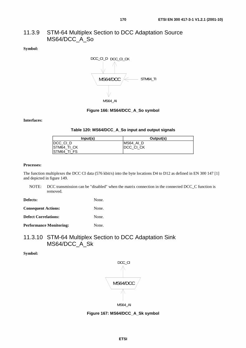
ETSI
ETSI EN 300 417-3-1 V1.2.1 (2001-10)170
11.3.9 STM-64 Multiplex Section to DCC Adaptation Source MS64/DCC_A_So
Symbol:
MS64/DCC
DCC_CI_D
MS64_AI
STM64_TI
DCC_CI_CK
Figure 166: MS64/DCC_A_So symbol
Interfaces:
Table 120: MS64/DCC_A_So input and output signals
Input(s) Output(s) DCC_CI_D STM64_TI_CK STM64_TI_FS
MS64_AI_D DCC_CI_CK
Processes:
The function multiplexes the DCC CI data (576 kbit/s) into the byte locations D4 to D12 as defined in EN 300 147 [1] and depicted in figure 149.
NOTE: DCC transmission can be "disabled" when the matrix connection in the connected DCC_C function is removed.
Defects: None.
Consequent Actions: None.
Defect Correlations: None.
Performance Monitoring: None.
11.3.10 STM-64 Multiplex Section to DCC Adaptation Sink MS64/DCC_A_Sk
Symbol:
MS64/DCC
DCC_CI
MS64_AI
Figure 167: MS64/DCC_A_Sk symbol
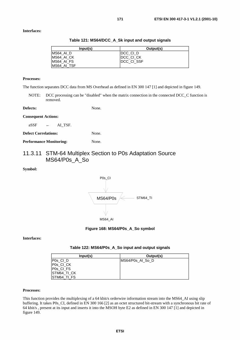
ETSI
ETSI EN 300 417-3-1 V1.2.1 (2001-10)171
Interfaces:
Table 121: MS64/DCC_A_Sk input and output signals
Input(s) Output(s) MS64_AI_D MS64_AI_CK MS64_AI_FS MS64_AI_TSF
DCC_CI_D DCC_CI_CK DCC_CI_SSF
Processes:
The function separates DCC data from MS Overhead as defined in EN 300 147 [1] and depicted in figure 149.
NOTE: DCC processing can be "disabled" when the matrix connection in the connected DCC_C function is removed.
Defects: None.
Consequent Actions:
aSSF ← AI_TSF.
Defect Correlations: None.
Performance Monitoring: None.
11.3.11 STM-64 Multiplex Section to P0s Adaptation Source MS64/P0s_A_So
Symbol:
MS64/P0s
P0s_CI
MS64_AI
STM64_TI
Figure 168: MS64/P0s_A_So symbol
Interfaces:
Table 122: MS64/P0s_A_So input and output signals
Input(s) Output(s) P0s_CI_D P0s_CI_CK P0s_CI_FS STM64_TI_CK STM64_TI_FS
MS64/P0s_AI_So_D
Processes:
This function provides the multiplexing of a 64 kbit/s orderwire information stream into the MS64_AI using slip buffering. It takes P0s_CI, defined in EN 300 166 [2] as an octet structured bit-stream with a synchronous bit rate of 64 kbit/s , present at its input and inserts it into the MSOH byte E2 as defined in EN 300 147 [1] and depicted in figure 149.

ETSI
ETSI EN 300 417-3-1 V1.2.1 (2001-10)172
NOTE: Any frequency deviation between the 64 kbit/s signal and the associated STM-64 signal leads to octet slips.
Frequency justification and bitrate adaptation: The function shall provide for an elastic store (slip buffer) process. The data signal shall be written into the store under control of the associated input clock. The data shall be read out of the store under control of the STM-64 clock, frame position, and justification decisions.
Each justification decision results in a corresponding negative / positive justification action. Upon a positive justification (slip) action, the reading of one 64 kbit/s octet (8 bits) shall be cancelled once. Upon a negative justification (slip) action, the same 64 kbit/s octet (8 bits) shall be read out a second time.
Buffer size: The elastic store (slip buffer) shall accommodate at least 18 µs of wander without introducing errors.
Defects: None.
Consequent Actions: None.
Defect Correlations: None.
Performance Monitoring: None.
11.3.12 STM-64 Multiplex Section to P0s Adaptation Sink MS64/P0s_A_Sk
Symbol:
MS64/P0s
P0s_CI
MS64_AI
Figure 169: MS64/P0s_A_Sk symbol
Interfaces:
Table 123: MS64/P0s_A_Sk input and output signals
Input(s) Output(s) MS64_AI_D MS64_AI_CK MS64_AI_FS MS64_AI_TSF
P0s_CI_Sk_D P0s_CI_Sk_CK P0s_CI_FS P0s_CI_SSF
Processes:
The function separates P0s data from MS Overhead byte E2 as defined in EN 300 147 [1] and depicted in figure 149.
Data latching and smoothing process: The function shall provide a data latching and smoothing function. Each 8-bit octet received shall be written and latched into a data store under the control of the STM-64 signal clock. The eight data bits shall then be read out of the store using a nominal 64 kHz clock which may be derived directly from the incoming STM-64 signal clock (e.g. 9 953 280 kHz divided by a factor of 155 520).
Defects: None.
Consequent Actions:
aSSF ← AI_TSF.
aAIS ← AI_TSF.
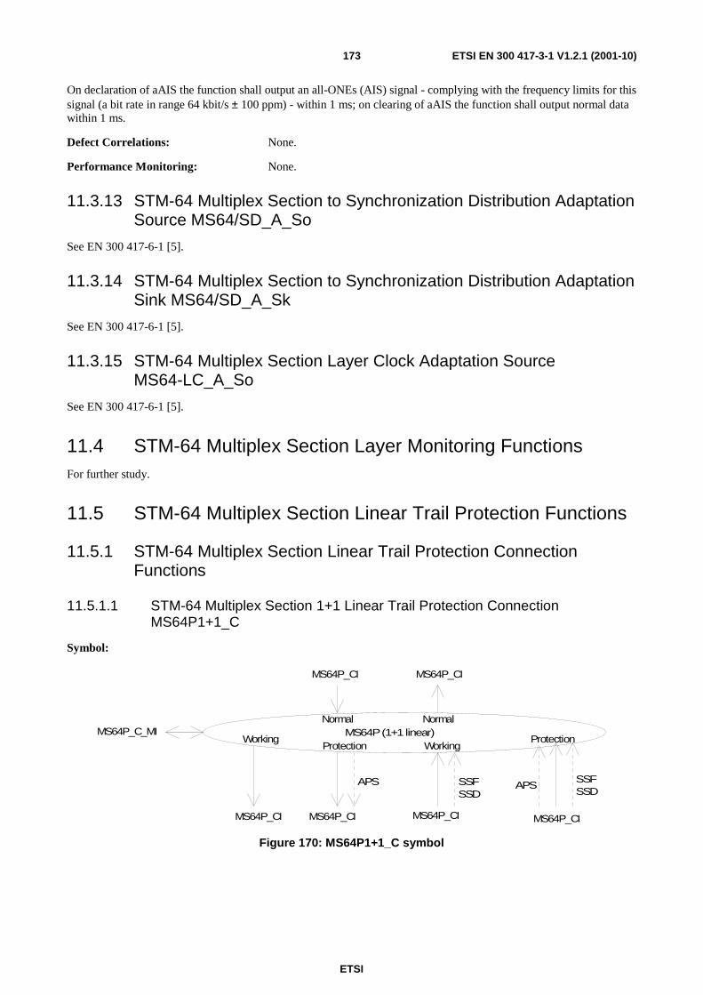
ETSI
ETSI EN 300 417-3-1 V1.2.1 (2001-10)173
On declaration of aAIS the function shall output an all-ONEs (AIS) signal - complying with the frequency limits for this signal (a bit rate in range 64 kbit/s ± 100 ppm) - within 1 ms; on clearing of aAIS the function shall output normal data within 1 ms.
Defect Correlations: None.
Performance Monitoring: None.
11.3.13 STM-64 Multiplex Section to Synchronization Distribution Adaptation Source MS64/SD_A_So
See EN 300 417-6-1 [5].
11.3.14 STM-64 Multiplex Section to Synchronization Distribution Adaptation Sink MS64/SD_A_Sk
See EN 300 417-6-1 [5].
11.3.15 STM-64 Multiplex Section Layer Clock Adaptation Source MS64-LC_A_So
See EN 300 417-6-1 [5].
11.4 STM-64 Multiplex Section Layer Monitoring Functions For further study.
11.5 STM-64 Multiplex Section Linear Trail Protection Functions
11.5.1 STM-64 Multiplex Section Linear Trail Protection Connection Functions
11.5.1.1 STM-64 Multiplex Section 1+1 Linear Trail Protection Connection MS64P1+1_C
Symbol:
MS64P_CI MS64P_CI
MS64P (1+1 linear)
APS SSFSSD
WorkingProtection Working
APSSSFSSD
Protection
MS64P_CI MS64P_CI
MS64P_CI MS64P_CI
Normal NormalMS64P_C_MI
Figure 170: MS64P1+1_C symbol

ETSI
ETSI EN 300 417-3-1 V1.2.1 (2001-10)174
Interfaces:
Table 124: MS64P1+1_C input and output signals
Input(s) Output(s) For connection points W and P: MS64P_CI_D MS64P_CI_CK MS64P_CI_FS MS64P_CI_SSF MS64P_CI_SSD For connection points N: MS64P_CI_D MS64P_CI_CK MS64P_CI_FS Per function: MS64P_CI_APS MS64P_C_MI_SWtype MS64P_C_MI_OPERtype MS64P_C_MI_WTRTime MS64P_C_MI_EXTCMD
For connection points W and P: MS64P_CI_D MS64P_CI_CK MS64P_CI_FS MS64P_CI_SSF For connection points N: MS64P_CI_D MS64P_CI_CK MS64P_CI_FS MS64P_CI_SSF Per function: MS64P_CI_APS MS64P_C_MI_cFOP
NOTE: Protection status reporting signals are for further study.
Processes:
The function performs the STM-64 linear multiplex section protection process for 1 + 1 protection architectures; see EN 300 417-1-1 [3], clause 9.2. It performs the bridge and selector functionality as presented in figure 48 of EN 300 417-1-1 [3]. In the sink direction, the signal output at the normal #1 reference point can be the signal received via either the associated working #1 section or the protection section; this is determined by the SF, SD conditions (relayed via CI_SSF, CI_SSD signals), the external commands and the information relayed via the APS signal. In the source direction, the working outputs are connected to the associated normal inputs. The protection output is outsourced (no input connected) or connected to any normal input.
Provided no protection switching action is activated / required the following changes to (the configuration of) a connection shall be possible without disturbing the CI passing the connection:
- change between switching types;
- change between operation types;
- change of WTR time.
MS Protection Operation: The MS trail protection process shall operate as specified in annex A, according the following characteristics.
Table 125: "Parameters for MS64P1+1_C protection process"
Architecture: 1 + 1 Switching type: uni-directional or bi-directional Operation type: revertive or non-revertive APS channel: 13 bits, K1[1-8] and K2[1-5] Wait-To-Restore time: in the order of 0-12 minutes Switching time: ≤ 50 ms Hold-off time: not applicable Signal switch conditions: SF, SD External commands: (revertive operation) LO, FSw-#1, MSw-#1, CLR, EXER-#1
(non-revertive operation) LO or FSw, FSw-#i, MSw, MSw-#i, CLR, EXER-#1
SFpriority, SDpriority: high
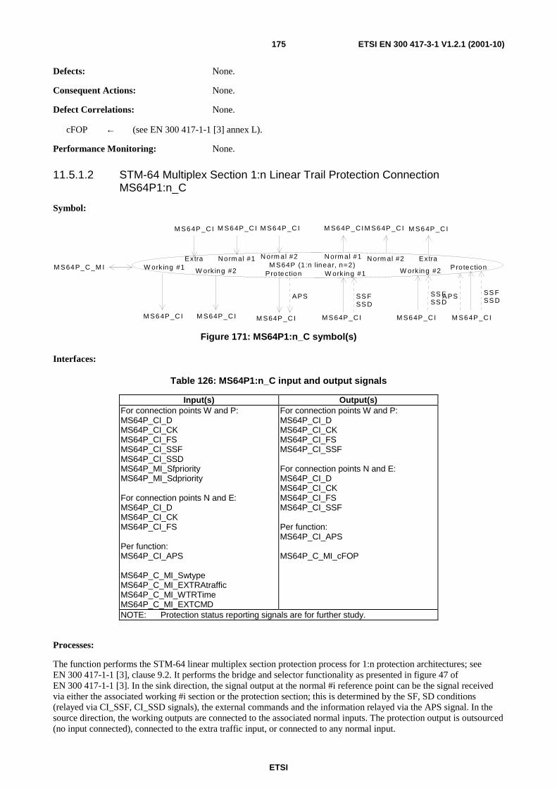
ETSI
ETSI EN 300 417-3-1 V1.2.1 (2001-10)175
Defects: None.
Consequent Actions: None.
Defect Correlations: None.
cFOP ← (see EN 300 417-1-1 [3] annex L).
Performance Monitoring: None.
11.5.1.2 STM-64 Multiplex Section 1:n Linear Trail Protection Connection MS64P1:n_C
Symbol:
M S64P _C I M S64P _C I
M S64P (1 :n linear, n=2)
APS SS FSS D
W orking #1Pro tection W orking #1
M S64P _C I
W orking #2
SS FSS D
W orking #2
APS SS FSS D
Protection
M S64P _C I M S64P_C I M S64P _C I
M S64P_C I M S64P _C I M S64P_CI M S64P _C I
M S64P_C _M INorm al #1 N orm al #2N orm al #1N orm al #2
M S64P _C I
Extra
M S64P _C I
Extra
Figure 171: MS64P1:n_C symbol(s)
Interfaces:
Table 126: MS64P1:n_C input and output signals
Input(s) Output(s) For connection points W and P: MS64P_CI_D MS64P_CI_CK MS64P_CI_FS MS64P_CI_SSF MS64P_CI_SSD MS64P_MI_Sfpriority MS64P_MI_Sdpriority For connection points N and E: MS64P_CI_D MS64P_CI_CK MS64P_CI_FS Per function: MS64P_CI_APS MS64P_C_MI_Swtype MS64P_C_MI_EXTRAtraffic MS64P_C_MI_WTRTime MS64P_C_MI_EXTCMD
For connection points W and P: MS64P_CI_D MS64P_CI_CK MS64P_CI_FS MS64P_CI_SSF For connection points N and E: MS64P_CI_D MS64P_CI_CK MS64P_CI_FS MS64P_CI_SSF Per function: MS64P_CI_APS MS64P_C_MI_cFOP
NOTE: Protection status reporting signals are for further study.
Processes:
The function performs the STM-64 linear multiplex section protection process for 1:n protection architectures; see EN 300 417-1-1 [3], clause 9.2. It performs the bridge and selector functionality as presented in figure 47 of EN 300 417-1-1 [3]. In the sink direction, the signal output at the normal #i reference point can be the signal received via either the associated working #i section or the protection section; this is determined by the SF, SD conditions (relayed via CI_SSF, CI_SSD signals), the external commands and the information relayed via the APS signal. In the source direction, the working outputs are connected to the associated normal inputs. The protection output is outsourced (no input connected), connected to the extra traffic input, or connected to any normal input.

ETSI
ETSI EN 300 417-3-1 V1.2.1 (2001-10)176
Provided no protection switching action is activated / required the following changes to (the configuration of) a connection shall be possible without disturbing the CI passing the connection:
- change between switching types;
- change of WTR time.
MS Protection Operation: The MS trail protection process shall operate as specified in annex A, according the following characteristics.
Table 127: "Parameters for MS64P1:n_C protection process"
Architecture: 1:n (n ≤ 14) Switching type: uni-directional or bi-directional Operation type: Revertive APS channel: 13 bits, K1[1-8] and K2[1-5] Wait-To-Restore time: in the order of 0-12 minutes Switching time: ≤ 50 ms Hold-off time: not applicable Signal switch conditions: SF, SD External commands: LO, FSw-#i, MSw-#i, CLR, EXER
Defects: None.
Consequent Actions:
For the case where neither the extra traffic nor a normal signal input is to be connected to the protection section output, the null signal shall be connected to the protection output. The null signal is either one of the normal signals, an all-ONEs, or a test signal.
For the case of a protection switch, the extra traffic output (if applicable) is disconnected from the protection input, set to all-ONEs (AIS) and aSSF is activated.
Defect Correlations:
cFOP ← (see EN 300 417-1-1 [3] annex L).
Performance Monitoring: None.
11.5.2 STM-64 Multiplex Section Linear Trail Protection Trail Termination Functions
11.5.2.1 Multiplex Section Protection Trail Termination Source MS64P_TT_So
Symbol:
M S 64 P
M S64_AI
M S64P_CI
M S64P_TT_So_M I
Figure 172: MS64P_TT_So symbol
ETSI
ETSI EN 300 417-3-1 V1.2.1 (2001-10)177
Interfaces:
Table 128: MS64P_TT_So input and output signals
Input(s) Output(s) MS64_AI_D MS64_AI_CK MS64_AI_FS
MS64P_CI_D MS64P_CI_CK MS64P_CI_FS
Processes:
No information processing is required in the MS64P_TT_So, the MS64_AI at its output being identical to the MS64P_CI at its input.
Defects: None.
Consequent Actions: None
Defect Correlations: None.
Performance Monitoring: None.
11.5.2.2 Multiplex Section Protection Trail Termination Sink MS64P_TT_Sk
Symbol:
M S 64P
M S64_AI
M S64P_CI
M S64P_TT_Sk_M I
Figure 173: MS64P_TT_Sk symbol
Interfaces:
Table 129: MS64P_TT_Sk input and output signals
Input(s) Output(s) MS64P_CI_D MS64P_CI_CK MS64P_CI_FS MS64P_CI_SSF MS64P_TT_Sk_MI_SSF_Reported
MS64_AI_D MS64_AI_CK MS64_AI_FS MS64_AI_TSF MS64P_TT_Sk_MI_cSSF
Processes:
The MS64P_TT_Sk function reports, as part of the MS64 layer, the state of the protected MS64 trail. In case all connections are unavailable the MS64P_TT_Sk reports the signal fail condition of the protected trail.
Defects: None.
Consequent Actions:
aTSF ← CI_SSF.

ETSI
ETSI EN 300 417-3-1 V1.2.1 (2001-10)178
Defect Correlations: None.
cSSF ← CI_SSF and SSF_Reported.
Performance Monitoring: None.
11.5.3 STM-64 Multiplex Section Linear Trail Protection Adaptation Functions
11.5.3.1 STM-64 Multiplex Section to STM-64 Multiplex Section Protection Layer Adaptation Source MS64/MS64P_A_So
Symbol:
M S64 /M S6 4P
M S64P _C I
M S64_A I
M S64/M S64P_A _So_M I
D C KFSA P S
Figure 174: MS64/MS64P_A_So symbol
Interfaces:
Table 130: MS64/MS64P_A_So input and output signals
Input(s) Output(s) MS64P_CI_D MS64P_CI_CK MS64P_CI_FS MS64P_CI_APS
MS64_AI_D MS64_AI_CK MS64_AI_FS
Processes:
The function shall multiplex the MS64 APS signal and MS64 data signal onto the MS64 access point.
Defects: None.
Consequent actions: None.
Defect Correlations: None.
Performance Monitoring: None.
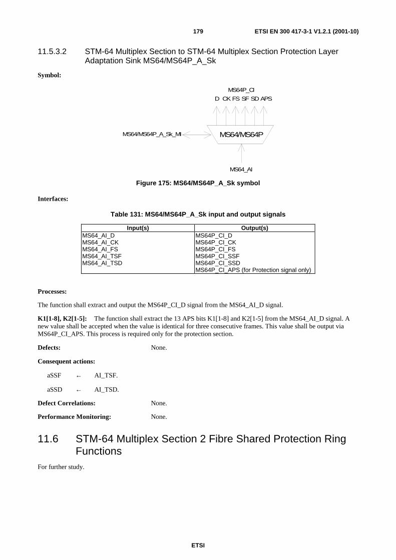
ETSI
ETSI EN 300 417-3-1 V1.2.1 (2001-10)179
11.5.3.2 STM-64 Multiplex Section to STM-64 Multiplex Section Protection Layer Adaptation Sink MS64/MS64P_A_Sk
Symbol:
MS64/MS64P
MS64P_CI
MS64_AI
MS64/MS64P_A_Sk_MI
D CK FS SF SD APS
Figure 175: MS64/MS64P_A_Sk symbol
Interfaces:
Table 131: MS64/MS64P_A_Sk input and output signals
Input(s) Output(s) MS64_AI_D MS64_AI_CK MS64_AI_FS MS64_AI_TSF MS64_AI_TSD
MS64P_CI_D MS64P_CI_CK MS64P_CI_FS MS64P_CI_SSF MS64P_CI_SSD MS64P_CI_APS (for Protection signal only)
Processes:
The function shall extract and output the MS64P_CI_D signal from the MS64_AI_D signal.
K1[1-8], K2[1-5]: The function shall extract the 13 APS bits K1[1-8] and K2[1-5] from the MS64_AI_D signal. A new value shall be accepted when the value is identical for three consecutive frames. This value shall be output via MS64P_CI_APS. This process is required only for the protection section.
Defects: None.
Consequent actions:
aSSF ← AI_TSF.
aSSD ← AI_TSD.
Defect Correlations: None.
Performance Monitoring: None.
11.6 STM-64 Multiplex Section 2 Fibre Shared Protection Ring Functions
For further study.
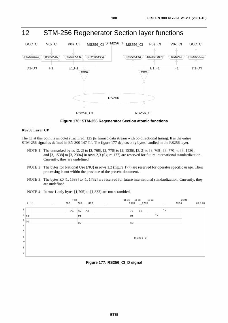
ETSI
ETSI EN 300 417-3-1 V1.2.1 (2001-10)180
12 STM-256 Regenerator Section layer functions
RS256
RS256/MS64
RS256
RS256/MS64
MS256_CI MS256_CI
RS256_CI RS256_CI
RS256/V0x RS256/V0xRS256/P0s-N
P0s_CISTM256_TI
RS256/P0s-N
P0s_CI
E1,F1 E1,F1
V0x_CIV0x_CI
RS256/DCC
DCC_CI
F1 D1-D3
RS256/DCC
DCC_CI
D1-D3 F1
RS256
Figure 176: STM-256 Regenerator Section atomic functions
RS256 Layer CP
The CI at this point is an octet structured, 125 µs framed data stream with co-directional timing. It is the entire STM-256 signal as defined in EN 300 147 [1]. The figure 177 depicts only bytes handled in the RS256 layer.
NOTE 1: The unmarked bytes [2, 2] to [2, 768], [2, 770] to [2, 1536], [3, 2] to [3, 768], [3, 770] to [3, 1536], and [3, 1538] to [3, 2304] in rows 2,3 (figure 177) are reserved for future international standardization. Currently, they are undefined.
NOTE 2: The bytes for National Use (NU) in rows 1,2 (figure 177) are reserved for operator specific usage. Their processing is not within the province of the present document.
NOTE 3: The bytes Z0 [1, 1538] to [1, 1792] are reserved for future international standardization. Currently, they are undefined.
NOTE 4: In row 1 only bytes [1,705] to [1,832] are not scrambled.
B1
D 1
A1 A2
E1
D2
A2 J 0 Z 0
F1
D3
1
2
3
4
5
6
7
8
9
NU
1 2 . .. 70 576 8
76 9 83 2 . ..
15 3615 37
15 3817 92
17 93
. .. 23 0423 05
69 1 20
M S25 6_C I
NU
. ... ..
Figure 177: RS256_CI_D signal
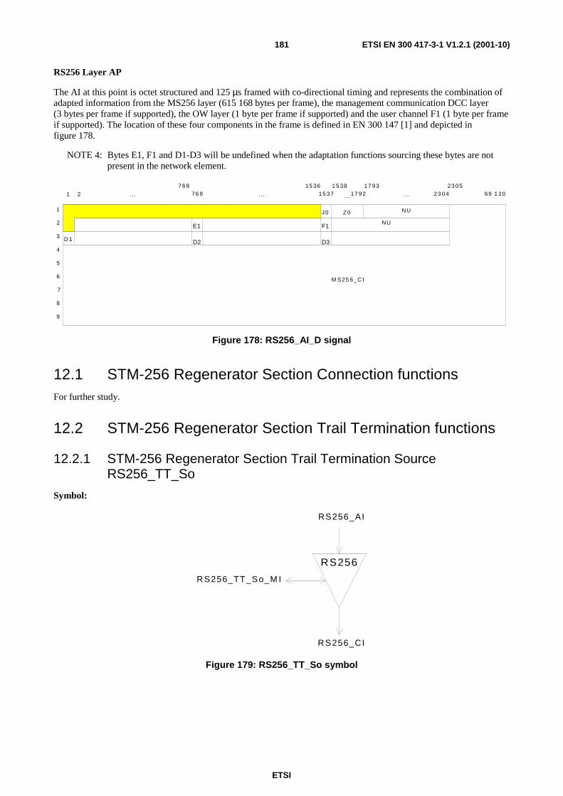
ETSI
ETSI EN 300 417-3-1 V1.2.1 (2001-10)181
RS256 Layer AP
The AI at this point is octet structured and 125 µs framed with co-directional timing and represents the combination of adapted information from the MS256 layer (615 168 bytes per frame), the management communication DCC layer (3 bytes per frame if supported), the OW layer (1 byte per frame if supported) and the user channel F1 (1 byte per frame if supported). The location of these four components in the frame is defined in EN 300 147 [1] and depicted in figure 178.
NOTE 4: Bytes E1, F1 and D1-D3 will be undefined when the adaptation functions sourcing these bytes are not present in the network element.
B1
D 1
A1 A2
E1
D2
A2 J 0 Z 0
F1
D3
1
2
3
4
5
6
7
8
9
NU
1 2 . ..
76 876 9 . ..
15 3615 37
15 3817 92
17 93
. .. 23 0423 05
69 1 20
M S25 6_C I
NU
. ..
Figure 178: RS256_AI_D signal
12.1 STM-256 Regenerator Section Connection functions For further study.
12.2 STM-256 Regenerator Section Trail Termination functions
12.2.1 STM-256 Regenerator Section Trail Termination Source RS256_TT_So
Symbol:
RS256
RS256_AI
R S256_CI
R S256_TT_So_M I
Figure 179: RS256_TT_So symbol
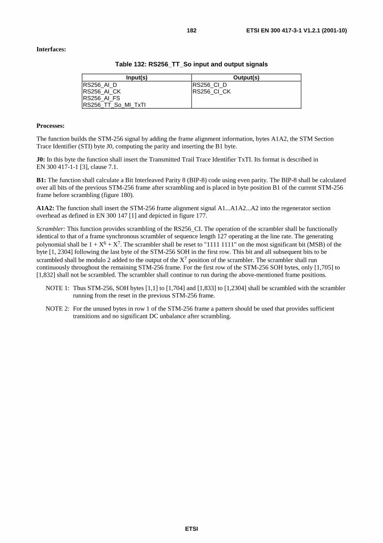
ETSI
ETSI EN 300 417-3-1 V1.2.1 (2001-10)182
Interfaces:
Table 132: RS256_TT_So input and output signals
Input(s) Output(s) RS256_AI_D RS256_AI_CK RS256_AI_FS RS256_TT_So_MI_TxTI
RS256_CI_D RS256_CI_CK
Processes:
The function builds the STM-256 signal by adding the frame alignment information, bytes A1A2, the STM Section Trace Identifier (STI) byte J0, computing the parity and inserting the B1 byte.
J0: In this byte the function shall insert the Transmitted Trail Trace Identifier TxTI. Its format is described in EN 300 417-1-1 [3], clause 7.1.
B1: The function shall calculate a Bit Interleaved Parity 8 (BIP-8) code using even parity. The BIP-8 shall be calculated over all bits of the previous STM-256 frame after scrambling and is placed in byte position B1 of the current STM-256 frame before scrambling (figure 180).
A1A2: The function shall insert the STM-256 frame alignment signal A1...A1A2...A2 into the regenerator section overhead as defined in EN 300 147 [1] and depicted in figure 177.
Scrambler: This function provides scrambling of the RS256_CI. The operation of the scrambler shall be functionally identical to that of a frame synchronous scrambler of sequence length 127 operating at the line rate. The generating polynomial shall be 1 + X6 + X7. The scrambler shall be reset to "1111 1111" on the most significant bit (MSB) of the byte [1, 2304] following the last byte of the STM-256 SOH in the first row. This bit and all subsequent bits to be scrambled shall be modulo 2 added to the output of the X7 position of the scrambler. The scrambler shall run continuously throughout the remaining STM-256 frame. For the first row of the STM-256 SOH bytes, only [1,705] to [1,832] shall not be scrambled. The scrambler shall continue to run during the above-mentioned frame positions.
NOTE 1: Thus STM-256, SOH bytes [1,1] to [1,704] and [1,833] to [1,2304] shall be scrambled with the scrambler running from the reset in the previous STM-256 frame.
NOTE 2: For the unused bytes in row 1 of the STM-256 frame a pattern should be used that provides sufficient transitions and no significant DC unbalance after scrambling.
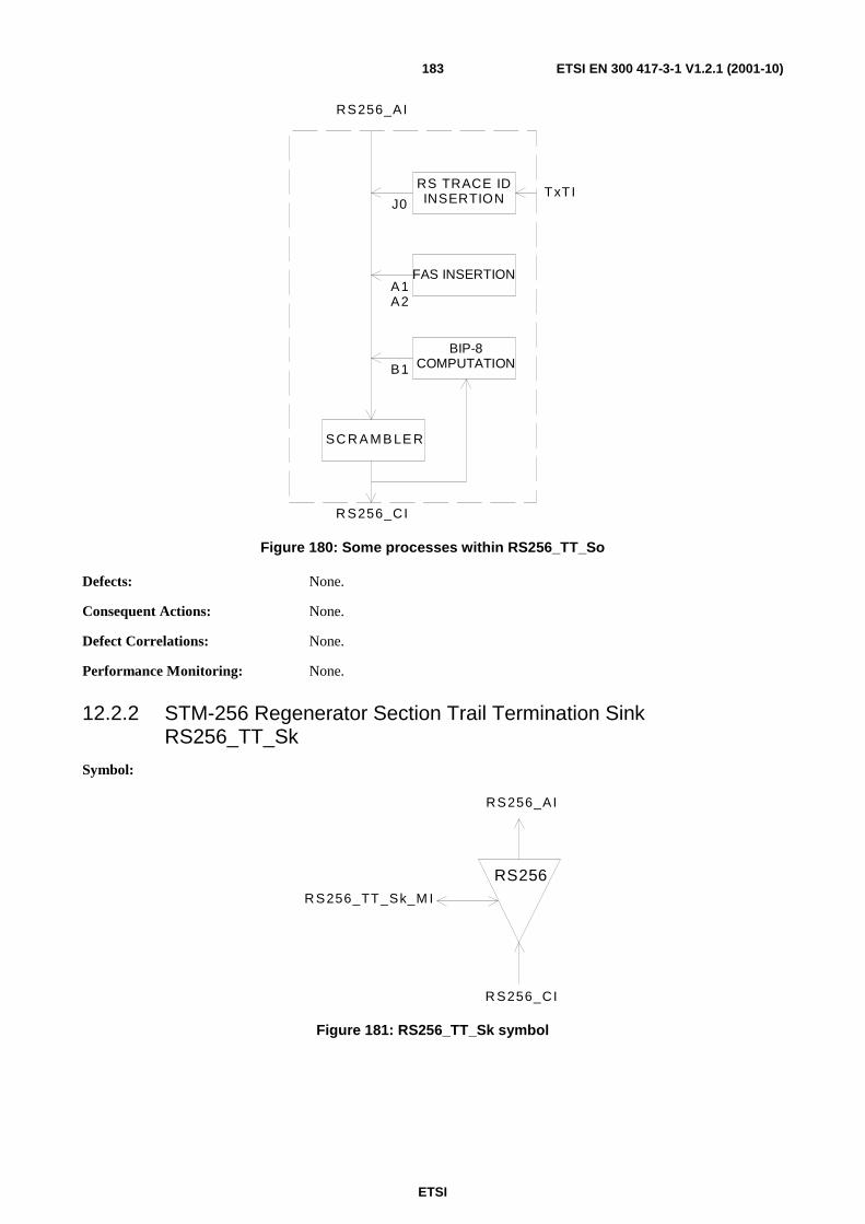
ETSI
ETSI EN 300 417-3-1 V1.2.1 (2001-10)183
SC R A M B LE R
BIP-8COMPUTATIONB1
R S256_CI
RS TRACE IDINSERTIONJ0
FAS INSERTION
RS256_AI
A1A2
TxTI
Figure 180: Some processes within RS256_TT_So
Defects: None.
Consequent Actions: None.
Defect Correlations: None.
Performance Monitoring: None.
12.2.2 STM-256 Regenerator Section Trail Termination Sink RS256_TT_Sk
Symbol:
RS256
RS256_AI
R S256_CI
R S256_TT_Sk_M I
Figure 181: RS256_TT_Sk symbol

ETSI
ETSI EN 300 417-3-1 V1.2.1 (2001-10)184
Interfaces:
Table 133: RS256_TT_Sk input and output signals
Input(s) Output(s) RS256_CI_D RS256_CI_CK RS256_CI_FS RS256_CI_SSF RS256_TT_Sk_MI_ExTI RS256_TT_Sk_MI_TPmode RS256_TT_Sk_MI_TIMdis RS256_TT_Sk_MI_ExTImode RS256_TT_Sk_MI_1second
RS256_AI_D RS256_AI_CK RS256_AI_FS RS256_AI_TSF RS256_TT_Sk_MI_AcTI RS256_TT_Sk_MI_cTIM RS256_TT_Sk_MI_pN_EBC RS256_TT_Sk_MI_pN_DS
Processes:
This function monitors the STM-256 signal for RS errors, and recovers the RS trail termination status. It extracts the payload independent overhead bytes (J0, B1) from the RS256 layer Characteristic Information:
Descrambling: The function shall descramble the incoming STM-256 signal. The operation of the descrambler shall be functionally identical to that of a scrambler in RS256_TT_So.
B1: Even bit parity is computed for each bit n of every byte of the preceding scrambled STM-256 frame and compared with bit n of B1 recovered from the current frame (n = 1 to 8 inclusive) (figure 182). A difference between the computed and recovered B1 values is taken as evidence of one or more errors (nN_B) in the computation block.
J0: The Received Trail Trace Identifier RxTI shall be recovered from the J0 byte and shall be made available as AcTI for network management purposes. The application and acceptance and mismatch detection process shall be performed as specified in EN 300 417-1-1 [3], clauses 7.1, and 8.2.1.3.
DESCRAMBLER
BIP-8COMPUTATION
B1
RS TRACE IDPROCESSJ0
R S256_CI
COMPARISON BIP-8vio la tions
AcTIdTIMExTI
RS256_AI
T IM disExTIm ode
Figure 182: Some processes within RS256_TT_Sk
Defects:
The function shall detect for dTIM defects according the specification in EN 300 417-1-1 [3], clause 8.2.1.
ETSI
ETSI EN 300 417-3-1 V1.2.1 (2001-10)185
Consequent Actions:
aAIS ← CI_SSF or dTIM.
aTSF ← CI_SSF or dTIM.
On declaration of aAIS the function shall output an all-ONEs (AIS) signal within 250 µs; on clearing of aAIS the function shall output normal data within 250 µs.
NOTE 1: The term "CI_SSF" has been added to the conditions for aAIS while the descrambler function has been moved from the e.g. OS256/RS256_A_Sk to this function. Consequently, an all-ONEs (AIS) pattern inserted in the mentioned adaptation function would be descrambled in this function. A "refreshment" of all-ONEs is required.
NOTE 2: The insertion of AIS - especially due to detection of dTIM - will cause the RS-DCC channel to be "squelched" too, so that control of the NE via this channel is lost. If control is via this channel only, there is a risk of a dead-lock situation if dTIM is caused by a misprovisioning of ExTI.
Defect Correlations:
cTIM ← MON and dTIM.
Performance Monitoring:
For further study.
12.3 STM-256 Regenerator Section Adaptation functions
12.3.1 STM-256 Regenerator Section to Multiplex Section Adaptation Source RS256/MS256_A_So
Symbol:
RS256/MS256
M S256_C I
RS256_AI
Figure 183: RS256/MS256_A_So symbol
Interfaces:
Table 134: RS256/MS256_A_So input and output signals
Input(s) Output(s) MS256_CI_D MS256_CI_CK STM256_CI_FS STM256_CI_SSF
RS256_AI_D RS256_AI_CK RS256_AI_FS
Processes:
The function multiplexes the MS256_CI data (615 168 bytes / frame) into the STM-256 byte locations defined in EN 300 147 [1] and depicted in figure 178.
ETSI
ETSI EN 300 417-3-1 V1.2.1 (2001-10)186
NOTE 1: There might be cases in which the network element knows that the timing reference for a particular STM-256 interface can not be maintained within ±4,6 ppm. For such cases MS-AIS can be generated. This is network element specific and outside the scope of the present document.
Defects: None.
Consequent Actions:
aAIS ← CI_SSF.
On declaration of aAIS the function shall output an all-ONEs signal within 250 µs; on clearing of aAIS the function shall output normal data within 250 µs. The frequency of the all ONEs signal shall be within 39 813 120 kHz ± 20 ppm.
NOTE 2: If CI_SSF is not connected (when RS256/MS256_A_So is connected to a MS256_TT_So), SSF is assumed to be false.
Defect Correlations: None.
Performance Monitoring: None.
12.3.2 STM-256 Regenerator Section to Multiplex Section Adaptation Sink RS256/MS256_A_Sk
Symbol:
RS256/MS256
M S256_C I
RS256_AI
Figure 184: RS256/MS256_A_Sk symbol
Interfaces:
Table 135: RS256/MS256_A_Sk input and output signals
Input(s) Output(s) RS256_AI_D RS256_AI_CK RS256_AI_FS RS256_AI_TSF
MS256_CI_D MS256_CI_CK MS256_CI_FS MS256_CI_SSF
Processes:
The function separates MS256_CI data from RS256_AI as depicted in figure 178.
Defects: None.
Consequent Actions:
aSSF ← AI_TSF.
Defect Correlations: None.
Performance Monitoring: None.
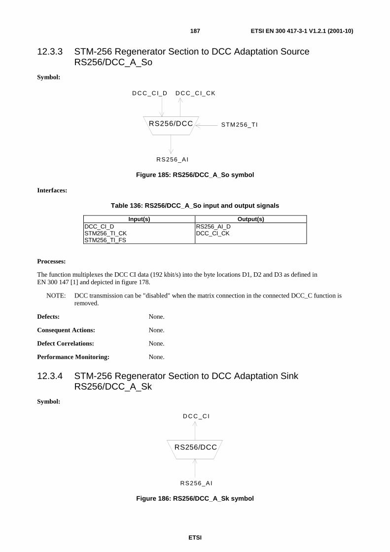
ETSI
ETSI EN 300 417-3-1 V1.2.1 (2001-10)187
12.3.3 STM-256 Regenerator Section to DCC Adaptation Source RS256/DCC_A_So
Symbol:
RS256/DCC
D C C_C I_D
RS256_AI
STM 256_TI
D C C _C I_CK
Figure 185: RS256/DCC_A_So symbol
Interfaces:
Table 136: RS256/DCC_A_So input and output signals
Input(s) Output(s) DCC_CI_D STM256_TI_CK STM256_TI_FS
RS256_AI_D DCC_CI_CK
Processes:
The function multiplexes the DCC CI data (192 kbit/s) into the byte locations D1, D2 and D3 as defined in EN 300 147 [1] and depicted in figure 178.
NOTE: DCC transmission can be "disabled" when the matrix connection in the connected DCC_C function is removed.
Defects: None.
Consequent Actions: None.
Defect Correlations: None.
Performance Monitoring: None.
12.3.4 STM-256 Regenerator Section to DCC Adaptation Sink RS256/DCC_A_Sk
Symbol:
RS256/DCC
D C C _C I
RS256_AI
Figure 186: RS256/DCC_A_Sk symbol

ETSI
ETSI EN 300 417-3-1 V1.2.1 (2001-10)188
Interfaces:
Table 137: RS256/DCC_A_Sk input and output signals
Input(s) Output(s) RS256_AI_D RS256_AI_CK RS256_AI_FS RS256_AI_TSF
DCC_CI_D DCC_CI_CK DCC_CI_SSF
Processes:
The function separates DCC data from RS Overhead as defined in EN 300 147 [1] and depicted in figure 178.
NOTE: DCC transmission can be "disabled" when the matrix connection in the connected DCC_C function is removed.
Defects: None.
Consequent Actions:
aSSF ← AI_TSF.
Defect Correlations: None.
Performance Monitoring: None.
12.3.5 STM-256 Regenerator Section to P0s Adaptation Source RS256/P0s_A_So/N
Symbol:
RS256/P0s-N
P0s_CI
RS256_AI
STM256_TI
N=E1,F1
Figure 187: RS256/P0s_A_So symbol
Interfaces:
Table 138: RS256/P0s_A_So input and output signals
Input(s) Output(s) P0s_CI_D P0s_CI_CK P0s_CI_FS MS256_TI_CK MS256_TI_FS
RS256_AI_D
Processes:
This function provides the multiplexing of a 64 kbit/s orderwire or user channel information stream into the RS256_AI using slip buffering. It takes P0s_CI, defined in EN 300 166 [2] as an octet structured bit-stream with a synchronous bit rate of 64 kbit/s, present at its input and inserts it into the RSOH byte E1 or F1 as defined in EN 300 147 [1] and depicted in figure 178.
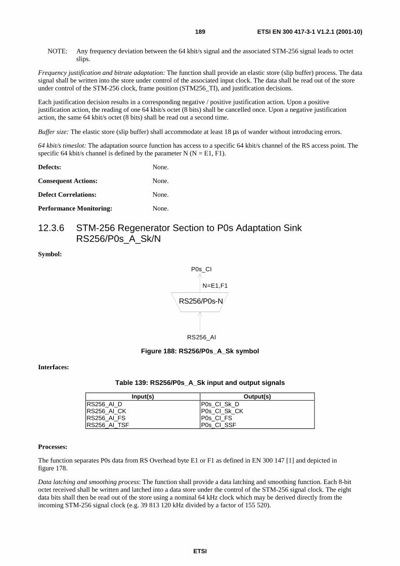
ETSI
ETSI EN 300 417-3-1 V1.2.1 (2001-10)189
NOTE: Any frequency deviation between the 64 kbit/s signal and the associated STM-256 signal leads to octet slips.
Frequency justification and bitrate adaptation: The function shall provide an elastic store (slip buffer) process. The data signal shall be written into the store under control of the associated input clock. The data shall be read out of the store under control of the STM-256 clock, frame position (STM256_TI), and justification decisions.
Each justification decision results in a corresponding negative / positive justification action. Upon a positive justification action, the reading of one 64 kbit/s octet (8 bits) shall be cancelled once. Upon a negative justification action, the same 64 kbit/s octet (8 bits) shall be read out a second time.
Buffer size: The elastic store (slip buffer) shall accommodate at least 18 µs of wander without introducing errors.
64 kbit/s timeslot: The adaptation source function has access to a specific 64 kbit/s channel of the RS access point. The specific 64 kbit/s channel is defined by the parameter N (N = E1, F1).
Defects: None.
Consequent Actions: None.
Defect Correlations: None.
Performance Monitoring: None.
12.3.6 STM-256 Regenerator Section to P0s Adaptation Sink RS256/P0s_A_Sk/N
Symbol:
RS256/P0s-N
P0s_CI
RS256_AI
N=E1,F1
Figure 188: RS256/P0s_A_Sk symbol
Interfaces:
Table 139: RS256/P0s_A_Sk input and output signals
Input(s) Output(s) RS256_AI_D RS256_AI_CK RS256_AI_FS RS256_AI_TSF
P0s_CI_Sk_D P0s_CI_Sk_CK P0s_CI_FS P0s_CI_SSF
Processes:
The function separates P0s data from RS Overhead byte E1 or F1 as defined in EN 300 147 [1] and depicted in figure 178.
Data latching and smoothing process: The function shall provide a data latching and smoothing function. Each 8-bit octet received shall be written and latched into a data store under the control of the STM-256 signal clock. The eight data bits shall then be read out of the store using a nominal 64 kHz clock which may be derived directly from the incoming STM-256 signal clock (e.g. 39 813 120 kHz divided by a factor of 155 520).
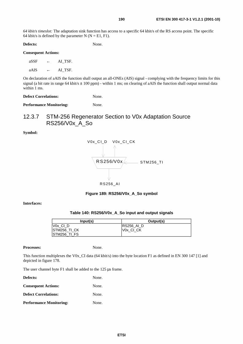
ETSI
ETSI EN 300 417-3-1 V1.2.1 (2001-10)190
64 kbit/s timeslot: The adaptation sink function has access to a specific 64 kbit/s of the RS access point. The specific 64 kbit/s is defined by the parameter N (N = E1, F1).
Defects: None.
Consequent Actions:
aSSF ← AI_TSF.
aAIS ← AI_TSF.
On declaration of aAIS the function shall output an all-ONEs (AIS) signal - complying with the frequency limits for this signal (a bit rate in range 64 kbit/s ± 100 ppm) - within 1 ms; on clearing of aAIS the function shall output normal data within 1 ms.
Defect Correlations: None.
Performance Monitoring: None.
12.3.7 STM-256 Regenerator Section to V0x Adaptation Source RS256/V0x_A_So
Symbol:
RS256/V0x
RS256_AI
STM 256_TI
V0x_C I_D V0x_CI_CK
Figure 189: RS256/V0x_A_So symbol
Interfaces:
Table 140: RS256/V0x_A_So input and output signals
Input(s) Output(s) V0x_CI_D STM256_TI_CK STM256_TI_FS
RS256_AI_D V0x_CI_CK
Processes: None.
This function multiplexes the V0x_CI data (64 kbit/s) into the byte location F1 as defined in EN 300 147 [1] and depicted in figure 178.
The user channel byte F1 shall be added to the 125 µs frame.
Defects: None.
Consequent Actions: None.
Defect Correlations: None.
Performance Monitoring: None.
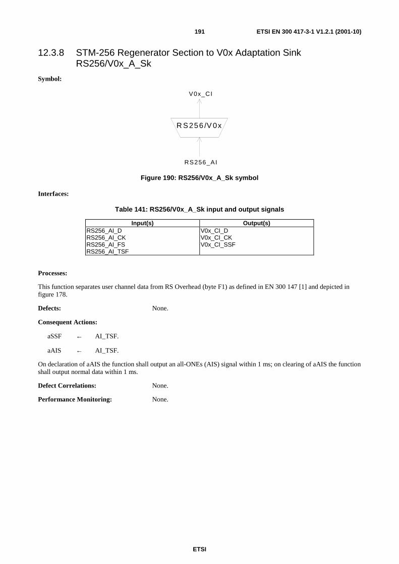
ETSI
ETSI EN 300 417-3-1 V1.2.1 (2001-10)191
12.3.8 STM-256 Regenerator Section to V0x Adaptation Sink RS256/V0x_A_Sk
Symbol:
R S256 /V 0x
V0x_CI
RS256_AI
Figure 190: RS256/V0x_A_Sk symbol
Interfaces:
Table 141: RS256/V0x_A_Sk input and output signals
Input(s) Output(s) RS256_AI_D RS256_AI_CK RS256_AI_FS RS256_AI_TSF
V0x_CI_D V0x_CI_CK V0x_CI_SSF
Processes:
This function separates user channel data from RS Overhead (byte F1) as defined in EN 300 147 [1] and depicted in figure 178.
Defects: None.
Consequent Actions:
aSSF ← AI_TSF.
aAIS ← AI_TSF.
On declaration of aAIS the function shall output an all-ONEs (AIS) signal within 1 ms; on clearing of aAIS the function shall output normal data within 1 ms.
Defect Correlations: None.
Performance Monitoring: None.
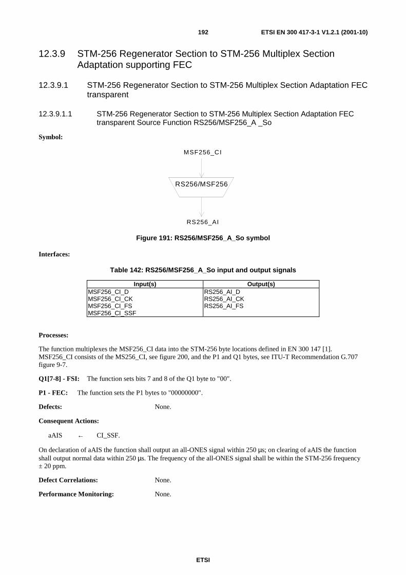
ETSI
ETSI EN 300 417-3-1 V1.2.1 (2001-10)192
12.3.9 STM-256 Regenerator Section to STM-256 Multiplex Section Adaptation supporting FEC
12.3.9.1 STM-256 Regenerator Section to STM-256 Multiplex Section Adaptation FEC transparent
12.3.9.1.1 STM-256 Regenerator Section to STM-256 Multiplex Section Adaptation FEC transparent Source Function RS256/MSF256_A _So
Symbol:
RS256/MSF256
MSF256_CI
RS256_AI
Figure 191: RS256/MSF256_A_So symbol
Interfaces:
Table 142: RS256/MSF256_A_So input and output signals
Input(s) Output(s) MSF256_CI_D MSF256_CI_CK MSF256_CI_FS MSF256_CI_SSF
RS256_AI_D RS256_AI_CK RS256_AI_FS
Processes:
The function multiplexes the MSF256_CI data into the STM-256 byte locations defined in EN 300 147 [1]. MSF256_CI consists of the MS256_CI, see figure 200, and the P1 and Q1 bytes, see ITU-T Recommendation G.707 figure 9-7.
Q1[7-8] - FSI: The function sets bits 7 and 8 of the Q1 byte to "00".
P1 - FEC: The function sets the P1 bytes to "00000000".
Defects: None.
Consequent Actions:
aAIS ← CI_SSF.
On declaration of aAIS the function shall output an all-ONES signal within 250 µs; on clearing of aAIS the function shall output normal data within 250 µs. The frequency of the all-ONES signal shall be within the STM-256 frequency ± 20 ppm.
Defect Correlations: None.
Performance Monitoring: None.
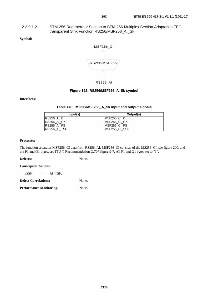
ETSI
ETSI EN 300 417-3-1 V1.2.1 (2001-10)193
12.3.9.1.2 STM-256 Regenerator Section to STM-256 Multiplex Section Adaptation FEC transparent Sink Function RS256/MSF256_A _Sk
Symbol:
RS256/MSF256
MSF256_CI
RS256_AI
Figure 192: RS256/MSF256_A_Sk symbol
Interfaces:
Table 143: RS256/MSF256_A_Sk input and output signals
Input(s) Output(s) RS256_AI_D RS256_AI_CK RS256_AI_FS RS256_AI_TSF
MSF256_CI_D MSF256_CI_CK MSF256_CI_FS MSF256_CI_SSF
Processes:
The function separates MSF256_CI data from RS256_AI. MSF256_CI consists of the MS256_CI, see figure 200, and the P1 and Q1 bytes, see ITU-T Recommendation G.707 figure 9-7. All P1 and Q1 bytes set to "1".
Defects: None.
Consequent Actions:
aSSF ← AI_TSF.
Defect Correlations: None.
Performance Monitoring: None.
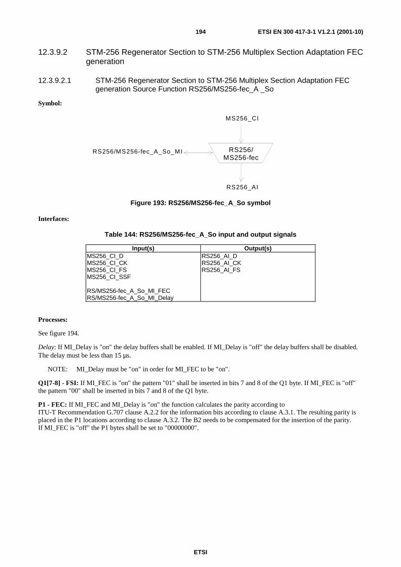
ETSI
ETSI EN 300 417-3-1 V1.2.1 (2001-10)194
12.3.9.2 STM-256 Regenerator Section to STM-256 Multiplex Section Adaptation FEC generation
12.3.9.2.1 STM-256 Regenerator Section to STM-256 Multiplex Section Adaptation FEC generation Source Function RS256/MS256-fec_A _So
Symbol:
RS256/MS256-fec
MS256_CI
RS256_AI
RS256/MS256-fec_A_So_MI
Figure 193: RS256/MS256-fec_A_So symbol
Interfaces:
Table 144: RS256/MS256-fec_A_So input and output signals
Input(s) Output(s) MS256_CI_D MS256_CI_CK MS256_CI_FS MS256_CI_SSF RS/MS256-fec_A_So_MI_FEC RS/MS256-fec_A_So_MI_Delay
RS256_AI_D RS256_AI_CK RS256_AI_FS
Processes:
See figure 194.
Delay: If MI_Delay is "on" the delay buffers shall be enabled. If MI_Delay is "off" the delay buffers shall be disabled. The delay must be less than 15 µs.
NOTE: MI_Delay must be "on" in order for MI_FEC to be "on".
Q1[7-8] - FSI: If MI_FEC is "on" the pattern "01" shall be inserted in bits 7 and 8 of the Q1 byte. If MI_FEC is "off" the pattern "00" shall be inserted in bits 7 and 8 of the Q1 byte.
P1 - FEC: If MI_FEC and MI_Delay is "on" the function calculates the parity according to ITU-T Recommendation G.707 clause A.2.2 for the information bits according to clause A.3.1. The resulting parity is placed in the P1 locations according to clause A.3.2. The B2 needs to be compensated for the insertion of the parity. If MI_FEC is "off" the P1 bytes shall be set to "00000000".

ETSI
ETSI EN 300 417-3-1 V1.2.1 (2001-10)195
data in
delaybuffer
FECencoding
B2
com
pe
nsa
tion
data out
on/off
on/o
ff
+
+
Figure 194: STM-256 FEC encoding process
Due to the insertion of the parity in the P1 bytes, BIP compensation should be done as shown in figure 195. The BIP is calculated before and after the overhead insertion. Both results and the related incoming BIP overhead (which is usually transported in the following frame) are combined via an exclusive OR and form the new BIP overhead for the outgoing signal. The related processes are shown in figure 196.
NOTE: The FEC calculation is done after the B2 compensation and includes the compensated B2 as shown in figure 195.
frame i
frame i+1
calc.BIP
frame i
frame i+1
calc.FEC
incoming signal B2 compensation
exclusive OR
SOH SOH
B2 B2'
frame i
frame i+1
calc.BIP
FEC insertionoutgoing signal
SOHwithFEC
SOHwithFEC
B2'
B2'calc.FEC
SOH
calc.BIP
calc.BIP
B2
SOH
B2'
Figure 195: B2 compensation and FEC calculation
new overhead
incoming signal outgoing signal
exclusive OR
overwrite overhead
insert BIP overhead
calculate BIP
extract BIP overhead
calculate BIP
one frame buffer
Figure 196: B2 correction; processes
Defects: None.
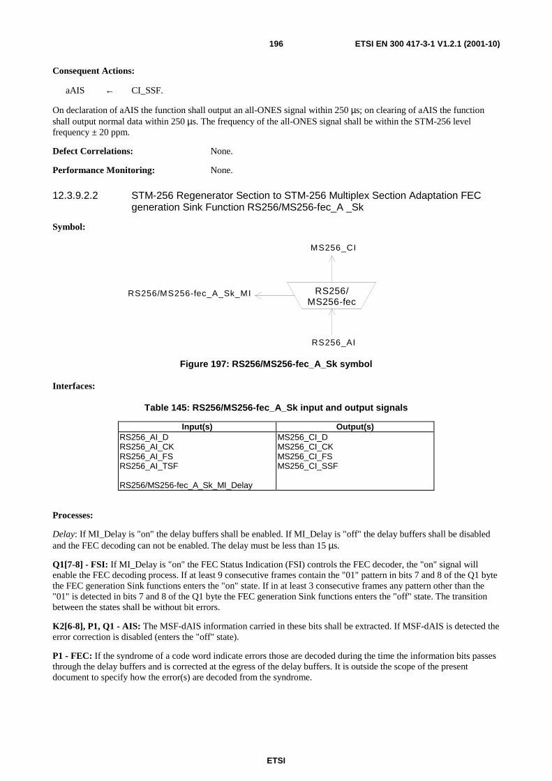
ETSI
ETSI EN 300 417-3-1 V1.2.1 (2001-10)196
Consequent Actions:
aAIS ← CI_SSF.
On declaration of aAIS the function shall output an all-ONES signal within 250 µs; on clearing of aAIS the function shall output normal data within 250 µs. The frequency of the all-ONES signal shall be within the STM-256 level frequency ± 20 ppm.
Defect Correlations: None.
Performance Monitoring: None.
12.3.9.2.2 STM-256 Regenerator Section to STM-256 Multiplex Section Adaptation FEC generation Sink Function RS256/MS256-fec_A _Sk
Symbol:
RS256/MS256-fec
MS256_CI
RS256_AI
RS256/MS256-fec_A_Sk_MI
Figure 197: RS256/MS256-fec_A_Sk symbol
Interfaces:
Table 145: RS256/MS256-fec_A_Sk input and output signals
Input(s) Output(s) RS256_AI_D RS256_AI_CK RS256_AI_FS RS256_AI_TSF RS256/MS256-fec_A_Sk_MI_Delay
MS256_CI_D MS256_CI_CK MS256_CI_FS MS256_CI_SSF
Processes:
Delay: If MI_Delay is "on" the delay buffers shall be enabled. If MI_Delay is "off" the delay buffers shall be disabled and the FEC decoding can not be enabled. The delay must be less than 15 µs.
Q1[7-8] - FSI: If MI_Delay is "on" the FEC Status Indication (FSI) controls the FEC decoder, the "on" signal will enable the FEC decoding process. If at least 9 consecutive frames contain the "01" pattern in bits 7 and 8 of the Q1 byte the FEC generation Sink functions enters the "on" state. If in at least 3 consecutive frames any pattern other than the "01" is detected in bits 7 and 8 of the Q1 byte the FEC generation Sink functions enters the "off" state. The transition between the states shall be without bit errors.
K2[6-8], P1, Q1 - AIS: The MSF-dAIS information carried in these bits shall be extracted. If MSF-dAIS is detected the error correction is disabled (enters the "off" state).
P1 - FEC: If the syndrome of a code word indicate errors those are decoded during the time the information bits passes through the delay buffers and is corrected at the egress of the delay buffers. It is outside the scope of the present document to specify how the error(s) are decoded from the syndrome.
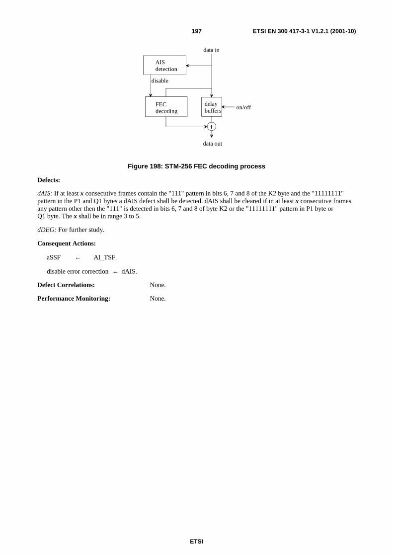
ETSI
ETSI EN 300 417-3-1 V1.2.1 (2001-10)197
data in
data out
on/off
disable
AIS detection
FEC decoding
delay buffers
Figure 198: STM-256 FEC decoding process
Defects:
dAIS: If at least x consecutive frames contain the "111" pattern in bits 6, 7 and 8 of the K2 byte and the "11111111" pattern in the P1 and Q1 bytes a dAIS defect shall be detected. dAIS shall be cleared if in at least x consecutive frames any pattern other then the "111" is detected in bits 6, 7 and 8 of byte K2 or the "11111111" pattern in P1 byte or Q1 byte. The x shall be in range 3 to 5.
dDEG: For further study.
Consequent Actions:
aSSF ← AI_TSF.
disable error correction ← dAIS.
Defect Correlations: None.
Performance Monitoring: None.
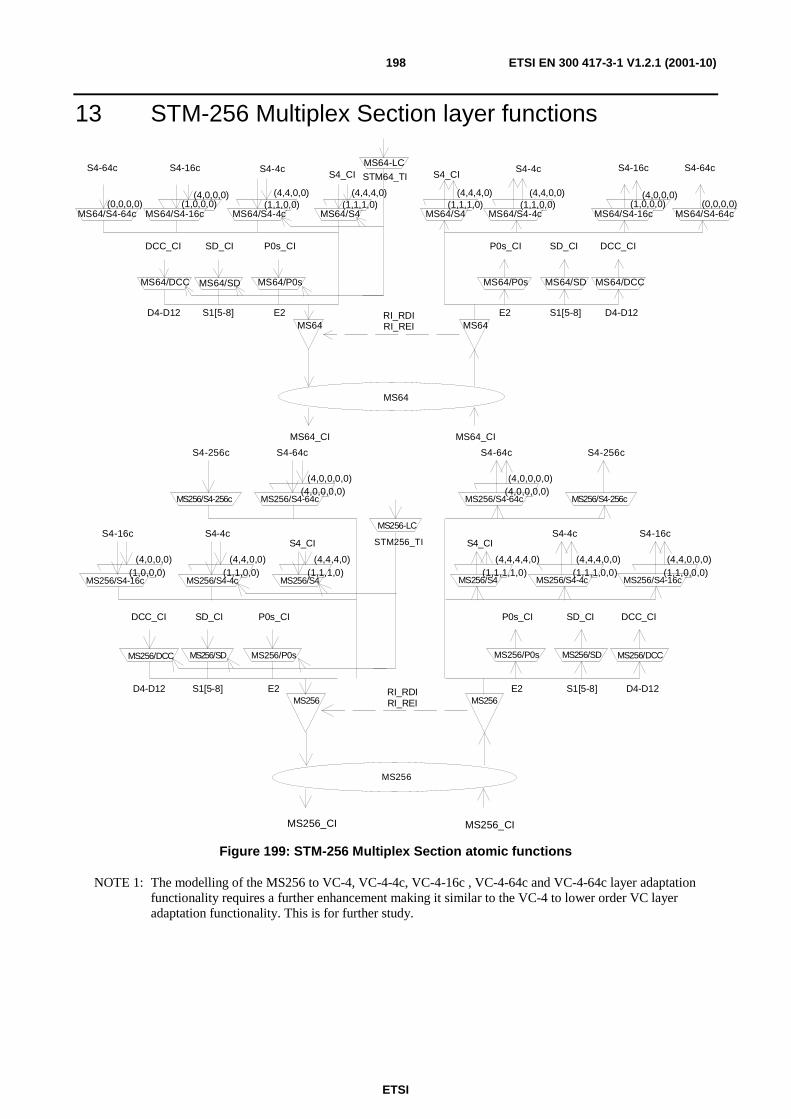
ETSI
ETSI EN 300 417-3-1 V1.2.1 (2001-10)198
13 STM-256 Multiplex Section layer functions
MS256_CI
P0s_CIP0s_CI
E2 E2
SD_CISD_CI DCC_CI
S1[5-8] D4-D12
MS256/DCC
DCC_CI
D4-D12 S1[5-8] RI_RDIRI_REI
S4_CIS4_CI
(1,1,1,0)
S4-4c S4-4c
MS256
MS256_CI
MS256MS256
MS256/SD MS256/P0s
MS256/S4MS256/S4-4cMS256/S4-16c
STM256_TI
MS256-LC
MS256/DCCMS256/SDMS256/P0s
MS256/S4 MS256/S4-4c MS256/S4-16c
(4,4,4,0)(4,4,0,0)(1,1,0,0)
(4,0,0,0)(1,0,0,0)
S4-16cS4-16c
(1,1,1,1,0)(4,4,4,4,0) (4,4,4,0,0)
(1,1,1,0,0)(4,4,0,0,0)
(1,1,0,0,0)
MS256/S4-64c
S4-64c
(4,0,0,0,0)(4,0,0,0,0)
MS256/S4-256c
S4-256c
MS256/S4-64c
S4-64c
(4,0,0,0,0)(4,0,0,0,0)
MS256/S4-256c
S4-256c
Figure 199: STM-256 Multiplex Section atomic functions
NOTE 1: The modelling of the MS256 to VC-4, VC-4-4c, VC-4-16c , VC-4-64c and VC-4-64c layer adaptation functionality requires a further enhancement making it similar to the VC-4 to lower order VC layer adaptation functionality. This is for further study.
MS64 MS64
MS64_CI MS64_CI
MS64/SD MS64/SDMS64/P0s
P0s_CI
STM64_TI
MS64/P0s
P0s_CI
E2 E2
SD_CISD_CI
MS64/DCC
DCC_CI
S1[5-8] D4-D12
MS64/DCC
DCC_CI
D4-D12 S1[5-8] RI_RDIRI_REI
S4_CI
MS64/S4
S4_CI
(1,1,1,0)(4,4,4,0)
S4-4c
MS64/S4(1,1,1,0)
(4,4,4,0)
S4-4c
MS64/S4-4c(1,1,0,0)
(4,4,0,0)
MS64/S4-4c(1,1,0,0)
(4,4,0,0)
MS64-LC
MS64
MS64/S4-64cMS64/S4-16c(1,0,0,0)
(4,0,0,0)(0,0,0,0)
S4-16c S4-64c
MS64/S4-16c(1,0,0,0)
(4,0,0,0)
S4-16c
MS64/S4-64c(0,0,0,0)
S4-64c
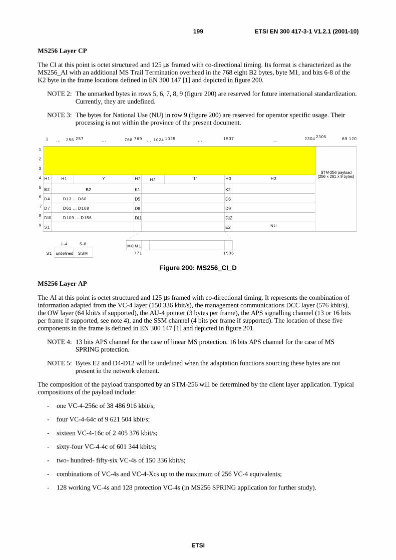
ETSI
ETSI EN 300 417-3-1 V1.2.1 (2001-10)199
MS256 Layer CP
The CI at this point is octet structured and 125 µs framed with co-directional timing. Its format is characterized as the MS256_AI with an additional MS Trail Termination overhead in the 768 eight B2 bytes, byte M1, and bits 6-8 of the K2 byte in the frame locations defined in EN 300 147 [1] and depicted in figure 200.
NOTE 2: The unmarked bytes in rows 5, 6, 7, 8, 9 (figure 200) are reserved for future international standardization. Currently, they are undefined.
NOTE 3: The bytes for National Use (NU) in row 9 (figure 200) are reserved for operator specific usage. Their processing is not within the province of the present document.
B2
D4
D7
D10
S1
B2 K1
D5
D8
D11
M 1
K2
D6
D9
D12
E2
1
2
3
4
5
6
7
8
9
H1 H1 H2 H3 H3
NU
'1'Y
1 257 769 1025 1537 2304 2305 69 120
STM-256 payload(256 x 261 x 9 bytes)
771 1536
H2
768256 1024.. . .. . .. . .. . .. .
SSMundefined
1-4 5-8
S1
M 0
D13 ... D60
D61 ... D108
D109 ... D156
Figure 200: MS256_CI_D
MS256 Layer AP
The AI at this point is octet structured and 125 µs framed with co-directional timing. It represents the combination of information adapted from the VC-4 layer (150 336 kbit/s), the management communications DCC layer (576 kbit/s), the OW layer (64 kbit/s if supported), the AU-4 pointer (3 bytes per frame), the APS signalling channel (13 or 16 bits per frame if supported, see note 4), and the SSM channel (4 bits per frame if supported). The location of these five components in the frame is defined in EN 300 147 [1] and depicted in figure 201.
NOTE 4: 13 bits APS channel for the case of linear MS protection. 16 bits APS channel for the case of MS SPRING protection.
NOTE 5: Bytes E2 and D4-D12 will be undefined when the adaptation functions sourcing these bytes are not present in the network element.
The composition of the payload transported by an STM-256 will be determined by the client layer application. Typical compositions of the payload include:
- one VC-4-256c of 38 486 916 kbit/s;
- four VC-4-64c of 9 621 504 kbit/s;
- sixteen VC-4-16c of 2 405 376 kbit/s;
- sixty-four VC-4-4c of 601 344 kbit/s;
- two- hundred- fifty-six VC-4s of 150 336 kbit/s;
- combinations of VC-4s and VC-4-Xcs up to the maximum of 256 VC-4 equivalents;
- 128 working VC-4s and 128 protection VC-4s (in MS256 SPRING application for further study).
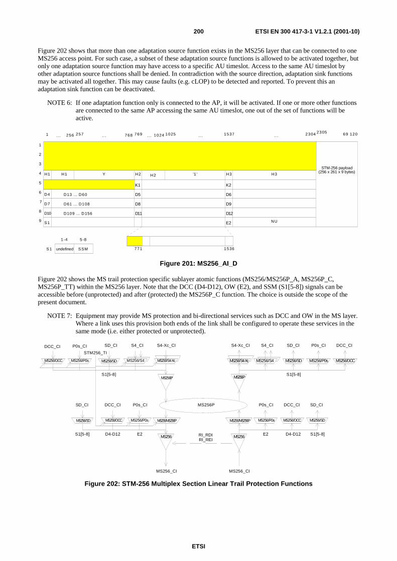
ETSI
ETSI EN 300 417-3-1 V1.2.1 (2001-10)200
Figure 202 shows that more than one adaptation source function exists in the MS256 layer that can be connected to one MS256 access point. For such case, a subset of these adaptation source functions is allowed to be activated together, but only one adaptation source function may have access to a specific AU timeslot. Access to the same AU timeslot by other adaptation source functions shall be denied. In contradiction with the source direction, adaptation sink functions may be activated all together. This may cause faults (e.g. cLOP) to be detected and reported. To prevent this an adaptation sink function can be deactivated.
NOTE 6: If one adaptation function only is connected to the AP, it will be activated. If one or more other functions are connected to the same AP accessing the same AU timeslot, one out of the set of functions will be active.
B2
D4
D7
D10
S1
B2 K1
D5
D8
D11
M 1
K2
D6
D9
D12
E2
1
2
3
4
5
6
7
8
9
H1 H1 H2 H3 H3
NU
'1'Y
1 257 769 1025 1537 2304 2305 69 120
STM-256 payload(256 x 261 x 9 bytes)
771 1536
H2
768256 1024.. . .. . .. . .. . .. .
SSMundefined
1-4 5-8
S1
D13 ... D60
D61 ... D108
D109 ... D156
Figure 201: MS256_AI_D
Figure 202 shows the MS trail protection specific sublayer atomic functions (MS256/MS256P_A, MS256P_C, MS256P_TT) within the MS256 layer. Note that the DCC (D4-D12), OW (E2), and SSM (S1[5-8]) signals can be accessible before (unprotected) and after (protected) the MS256P_C function. The choice is outside the scope of the present document.
NOTE 7: Equipment may provide MS protection and bi-directional services such as DCC and OW in the MS layer. Where a link uses this provision both ends of the link shall be configured to operate these services in the same mode (i.e. either protected or unprotected).
MS256
MS256/MS256P
MS256
MS256P
MS256_CI MS256_CI
MS256/P0s
P0s_CI
STM256_TI
MS256/P0s
P0s_CI
E2 E2
MS256/DCC
DCC_CI
D4-D12
MS256/DCC
DCC_CI
D4-D12 RI_RDIRI_REI
MS256/S4-Xc
S4-Xc_CI
MS256/S4-Xc
S4-Xc_CI
MS256/SD
SD_CI
S1[5-8]MS256P
S4_CI
MS256/S4MS256/P0sMS256/DCC
P0s_CIDCC_CI
MS256/P0s MS256/DCC
P0s_CI DCC_CI
MS256/SD
S1[5-8]
SD_CI
MS256/SD
S1[5-8]
SD_CI
MS256/SD
SD_CI
S1[5-8]
S4_CI
MS256/S4
MS256P
MS256/MS256P
Figure 202: STM-256 Multiplex Section Linear Trail Protection Functions
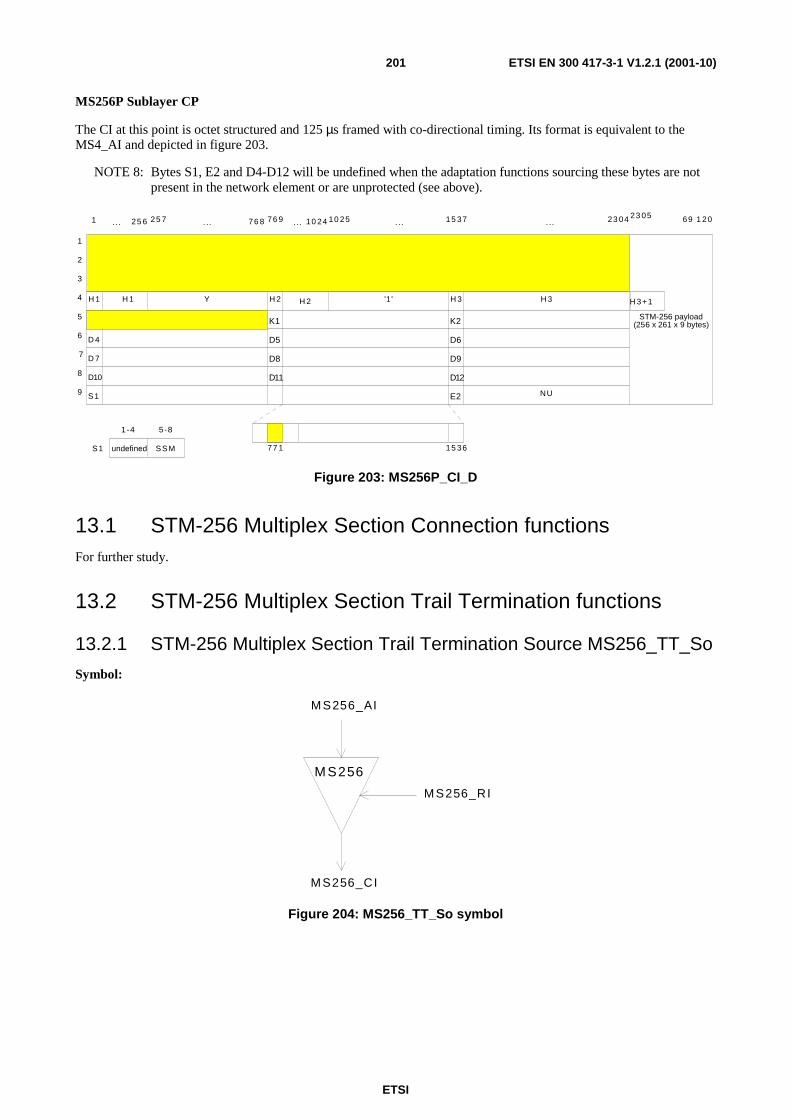
ETSI
ETSI EN 300 417-3-1 V1.2.1 (2001-10)201
MS256P Sublayer CP
The CI at this point is octet structured and 125 µs framed with co-directional timing. Its format is equivalent to the MS4_AI and depicted in figure 203.
NOTE 8: Bytes S1, E2 and D4-D12 will be undefined when the adaptation functions sourcing these bytes are not present in the network element or are unprotected (see above).
B2
D 4
D 7
D10
S1
B2 K1
D5
D8
D11
M 1
K2
D6
D9
D12
E2
1
2
3
4
5
6
7
8
9
H 1 H 1 H 2 H 3 H 3
NU
'1'Y
1 25 7 76 9 10 25 15 37 23 04 23 05 69 1 20
STM-256 payload(256 x 261 x 9 bytes)
77 1 15 36
H 2
76 825 6 10 24. .. . .. . .. . .. . ..
SSMundefined
1-4 5-8
S1
H 3+1
Figure 203: MS256P_CI_D
13.1 STM-256 Multiplex Section Connection functions For further study.
13.2 STM-256 Multiplex Section Trail Termination functions
13.2.1 STM-256 Multiplex Section Trail Termination Source MS256_TT_So
Symbol:
M S256_AI
M S256_CI
M S256_RI
M S256
Figure 204: MS256_TT_So symbol
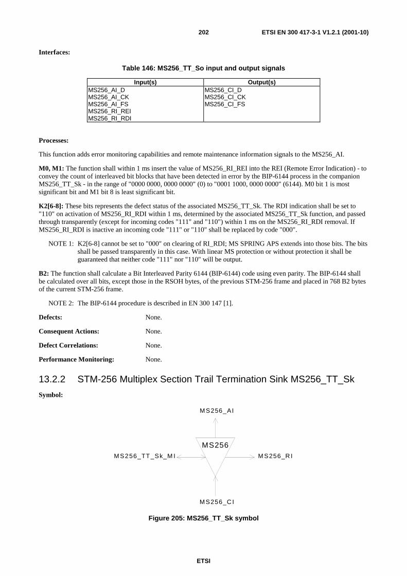
ETSI
ETSI EN 300 417-3-1 V1.2.1 (2001-10)202
Interfaces:
Table 146: MS256_TT_So input and output signals
Input(s) Output(s) MS256_AI_D MS256_AI_CK MS256_AI_FS MS256_RI_REI MS256_RI_RDI
MS256_CI_D MS256_CI_CK MS256_CI_FS
Processes:
This function adds error monitoring capabilities and remote maintenance information signals to the MS256_AI.
M0, M1: The function shall within 1 ms insert the value of MS256_RI_REI into the REI (Remote Error Indication) - to convey the count of interleaved bit blocks that have been detected in error by the BIP-6144 process in the companion MS256_TT_Sk - in the range of "0000 0000, 0000 0000" (0) to "0001 1000, 0000 0000" (6144). M0 bit 1 is most significant bit and M1 bit 8 is least significant bit.
K2[6-8]: These bits represents the defect status of the associated MS256_TT_Sk. The RDI indication shall be set to "110" on activation of MS256_RI_RDI within 1 ms, determined by the associated MS256_TT_Sk function, and passed through transparently (except for incoming codes "111" and "110") within 1 ms on the MS256_RI_RDI removal. If MS256_RI_RDI is inactive an incoming code "111" or "110" shall be replaced by code "000".
NOTE 1: K2[6-8] cannot be set to "000" on clearing of RI_RDI; MS SPRING APS extends into those bits. The bits shall be passed transparently in this case. With linear MS protection or without protection it shall be guaranteed that neither code "111" nor "110" will be output.
B2: The function shall calculate a Bit Interleaved Parity 6144 (BIP-6144) code using even parity. The BIP-6144 shall be calculated over all bits, except those in the RSOH bytes, of the previous STM-256 frame and placed in 768 B2 bytes of the current STM-256 frame.
NOTE 2: The BIP-6144 procedure is described in EN 300 147 [1].
Defects: None.
Consequent Actions: None.
Defect Correlations: None.
Performance Monitoring: None.
13.2.2 STM-256 Multiplex Section Trail Termination Sink MS256_TT_Sk
Symbol:
MS256
M S256_AI
M S256_C I
M S256_TT_Sk_M I M S256_R I
Figure 205: MS256_TT_Sk symbol
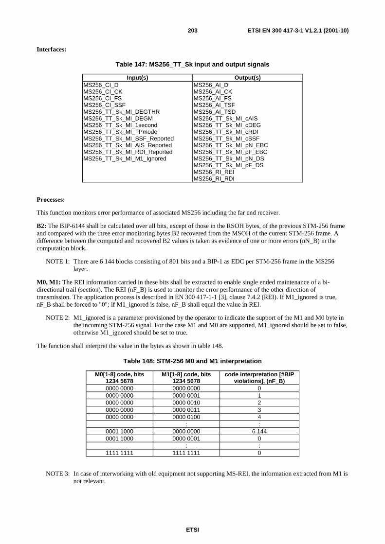
ETSI
ETSI EN 300 417-3-1 V1.2.1 (2001-10)203
Interfaces:
Table 147: MS256_TT_Sk input and output signals
Input(s) Output(s) MS256_CI_D MS256_CI_CK MS256_CI_FS MS256_CI_SSF MS256_TT_Sk_MI_DEGTHR MS256_TT_Sk_MI_DEGM MS256_TT_Sk_MI_1second MS256_TT_Sk_MI_TPmode MS256_TT_Sk_MI_SSF_Reported MS256_TT_Sk_MI_AIS_Reported MS256_TT_Sk_MI_RDI_Reported MS256_TT_Sk_MI_M1_Ignored
MS256_AI_D MS256_AI_CK MS256_AI_FS MS256_AI_TSF MS256_AI_TSD MS256_TT_Sk_MI_cAIS MS256_TT_Sk_MI_cDEG MS256_TT_Sk_MI_cRDI MS256_TT_Sk_MI_cSSF MS256_TT_Sk_MI_pN_EBC MS256_TT_Sk_MI_pF_EBC MS256_TT_Sk_MI_pN_DS MS256_TT_Sk_MI_pF_DS MS256_RI_REI MS256_RI_RDI
Processes:
This function monitors error performance of associated MS256 including the far end receiver.
B2: The BIP-6144 shall be calculated over all bits, except of those in the RSOH bytes, of the previous STM-256 frame and compared with the three error monitoring bytes B2 recovered from the MSOH of the current STM-256 frame. A difference between the computed and recovered B2 values is taken as evidence of one or more errors (nN_B) in the computation block.
NOTE 1: There are 6 144 blocks consisting of 801 bits and a BIP-1 as EDC per STM-256 frame in the MS256 layer.
M0, M1: The REI information carried in these bits shall be extracted to enable single ended maintenance of a bi-directional trail (section). The REI (nF_B) is used to monitor the error performance of the other direction of transmission. The application process is described in EN 300 417-1-1 [3], clause 7.4.2 (REI). If M1_ignored is true, nF_B shall be forced to "0"; if M1_ignored is false, nF_B shall equal the value in REI.
NOTE 2: M1_ignored is a parameter provisioned by the operator to indicate the support of the M1 and M0 byte in the incoming STM-256 signal. For the case M1 and M0 are supported, M1_ignored should be set to false, otherwise M1_ignored should be set to true.
The function shall interpret the value in the bytes as shown in table 148.
Table 148: STM-256 M0 and M1 interpretation
M0[1-8] code, bits 1234 5678
M1[1-8] code, bits 1234 5678
code interpretation [#BIP violations], (nF_B)
0000 0000 0000 0000 0 0000 0000 0000 0001 1 0000 0000 0000 0010 2 0000 0000 0000 0011 3 0000 0000 0000 0100 4
: : 0001 1000 0000 0000 6 144 0001 1000 0000 0001 0
: : 1111 1111 1111 1111 0
NOTE 3: In case of interworking with old equipment not supporting MS-REI, the information extracted from M1 is not relevant.
ETSI
ETSI EN 300 417-3-1 V1.2.1 (2001-10)204
K2[6-8] - RDI: The RDI information carried in these bits shall be extracted to enable single ended maintenance of a bi-directional trail (section). The RDI provides information as to the status of the remote receiver. A "110" indicates a Remote Defect Indication state, while other patterns indicate the normal state. The application process is described in EN 300 417-1-1 [3], clauses 7.4.11 and 8.2.
K2[6-8] - AIS: The MS-AIS information carried in these bits shall be extracted.
Defects:
The function shall detect for dDEG and dRDI defects according the specification in EN 300 417-1-1 [3], clause 8.2.1.
dAIS: If at least x consecutive frames contain the "111" pattern in bits 6, 7 and 8 of the K2 byte a dAIS defect shall be detected. dAIS shall be cleared if in at least x consecutive frames any pattern other then the "111" is detected in bits 6, 7 and 8 of byte K2. The x shall be in range 3 to 5.
Consequent Actions:
aAIS ← dAIS.
aRDI ← dAIS.
aREI ← #EDCV.
aTSF ← dAIS.
aTSD ← dDEG.
On declaration of aAIS the function shall output an all-ONEs signal within 250 µs; on clearing of aAIS the function shall output normal data within 250 µs.
Defect Correlations:
cAIS ← MON and dAIS and (not CI_SSF) and AIS_Reported.
cDEG ← MON and dDEG.
cRDI ← MON and dRDI and RDI_Reported.
cSSF ← MON and dAIS and SSF_Reported.
Performance monitoring:
The performance monitoring process shall be performed as specified in EN 300 417-1-1 [3], clause 8.2.4 through 8.2.7.
pN_DS ← aTSF or dEQ.
pF_DS ← dRDI.
pN_EBC ← Σ nN_B.
pF_EBC ← Σ nF_B.
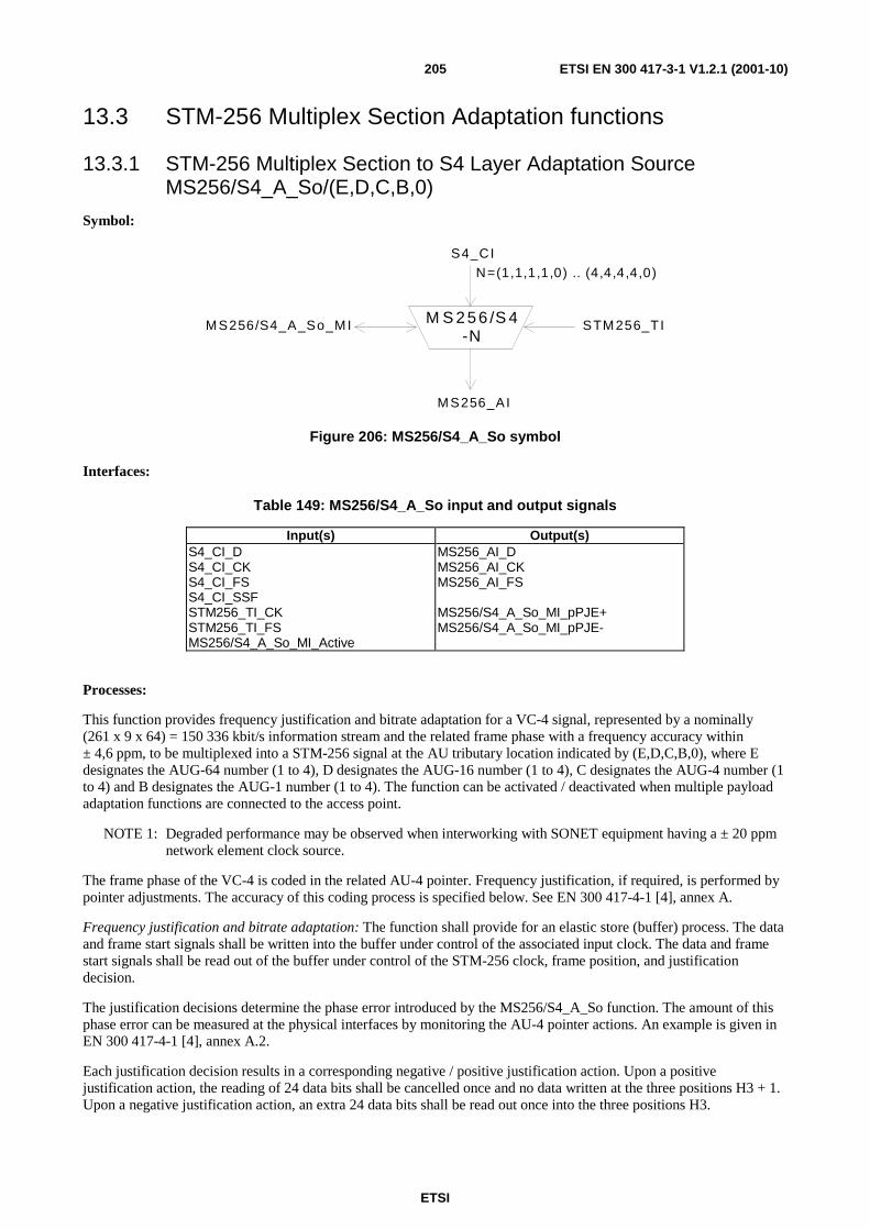
ETSI
ETSI EN 300 417-3-1 V1.2.1 (2001-10)205
13.3 STM-256 Multiplex Section Adaptation functions
13.3.1 STM-256 Multiplex Section to S4 Layer Adaptation Source MS256/S4_A_So/(E,D,C,B,0)
Symbol:
M S 256 /S 4-N
S4_CI
M S256_AI
M S256/S4_A_So_M I STM 256_TI
N=(1,1,1,1,0) .. (4,4,4,4,0)
Figure 206: MS256/S4_A_So symbol
Interfaces:
Table 149: MS256/S4_A_So input and output signals
Input(s) Output(s) S4_CI_D S4_CI_CK S4_CI_FS S4_CI_SSF STM256_TI_CK STM256_TI_FS MS256/S4_A_So_MI_Active
MS256_AI_D MS256_AI_CK MS256_AI_FS MS256/S4_A_So_MI_pPJE+ MS256/S4_A_So_MI_pPJE-
Processes:
This function provides frequency justification and bitrate adaptation for a VC-4 signal, represented by a nominally (261 x 9 x 64) = 150 336 kbit/s information stream and the related frame phase with a frequency accuracy within ± 4,6 ppm, to be multiplexed into a STM-256 signal at the AU tributary location indicated by (E,D,C,B,0), where E designates the AUG-64 number (1 to 4), D designates the AUG-16 number (1 to 4), C designates the AUG-4 number (1 to 4) and B designates the AUG-1 number (1 to 4). The function can be activated / deactivated when multiple payload adaptation functions are connected to the access point.
NOTE 1: Degraded performance may be observed when interworking with SONET equipment having a ± 20 ppm network element clock source.
The frame phase of the VC-4 is coded in the related AU-4 pointer. Frequency justification, if required, is performed by pointer adjustments. The accuracy of this coding process is specified below. See EN 300 417-4-1 [4], annex A.
Frequency justification and bitrate adaptation: The function shall provide for an elastic store (buffer) process. The data and frame start signals shall be written into the buffer under control of the associated input clock. The data and frame start signals shall be read out of the buffer under control of the STM-256 clock, frame position, and justification decision.
The justification decisions determine the phase error introduced by the MS256/S4_A_So function. The amount of this phase error can be measured at the physical interfaces by monitoring the AU-4 pointer actions. An example is given in EN 300 417-4-1 [4], annex A.2.
Each justification decision results in a corresponding negative / positive justification action. Upon a positive justification action, the reading of 24 data bits shall be cancelled once and no data written at the three positions H3 + 1. Upon a negative justification action, an extra 24 data bits shall be read out once into the three positions H3.
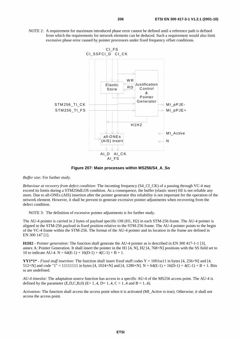
ETSI
ETSI EN 300 417-3-1 V1.2.1 (2001-10)206
NOTE 2: A requirement for maximum introduced phase error cannot be defined until a reference path is defined from which the requirements for network elements can be deduced. Such a requirement would also limit excessive phase error caused by pointer processors under fixed frequency offset conditions.
ElasticSto re
JustificationControl
&Pointer
G enerator
STM 256_TI_FS
STM 256_TI_CK
W R
R D
all-O NEs(AIS) insert
C I_SSFCI_DCI_FS
C I_C K
AI_DAI_FS
AI_C K
H 1H 2
M I_pPJE-
M I_pPJE+
M I_Active
N
Figure 207: Main processes within MS256/S4_A_So
Buffer size: For further study.
Behaviour at recovery from defect condition: The incoming frequency (S4_CI_CK) of a passing through VC-4 may exceed its limits during a STM256dLOS condition. As a consequence, the buffer (elastic store) fill is not reliable any more. Due to all-ONEs (AIS) insertion after the pointer generator this reliability is not important for the operation of the network element. However, it shall be prevent to generate excessive pointer adjustments when recovering from the defect condition.
NOTE 3: The definition of excessive pointer adjustments is for further study.
The AU-4 pointer is carried in 2 bytes of payload specific OH (H1, H2) in each STM-256 frame. The AU-4 pointer is aligned in the STM-256 payload in fixed position relative to the STM-256 frame. The AU-4 pointer points to the begin of the VC-4 frame within the STM-256. The format of the AU-4 pointer and its location in the frame are defined in EN 300 147 [1].
H1H2 - Pointer generation: The function shall generate the AU-4 pointer as is described in EN 300 417-1-1 [3], annex A: Pointer Generation. It shall insert the pointer in the H1 [4, N], H2 [4, 768+N] positions with the SS field set to 10 to indicate AU-4. N = 64(E-1) + 16(D-1) + 4(C-1) + B + 1.
YY1*1* - Fixed stuff insertion: The function shall insert fixed stuff codes Y = 1001ss11 in bytes [4, 256+N] and [4, 512+N] and code "1" = 11111111 in bytes [4, 1024+N] and [4, 1280+N]. N = 64(E-1) + 16(D-1) + 4(C-1) + B + 1. Bits ss are undefined.
AU-4 timeslot: The adaptation source function has access to a specific AU-4 of the MS256 access point. The AU-4 is defined by the parameter (E,D,C,B,0) (E= 1..4, D= 1..4, C = 1..4 and B = 1..4).
Activation: The function shall access the access point when it is activated (MI_Active is true). Otherwise, it shall not access the access point.
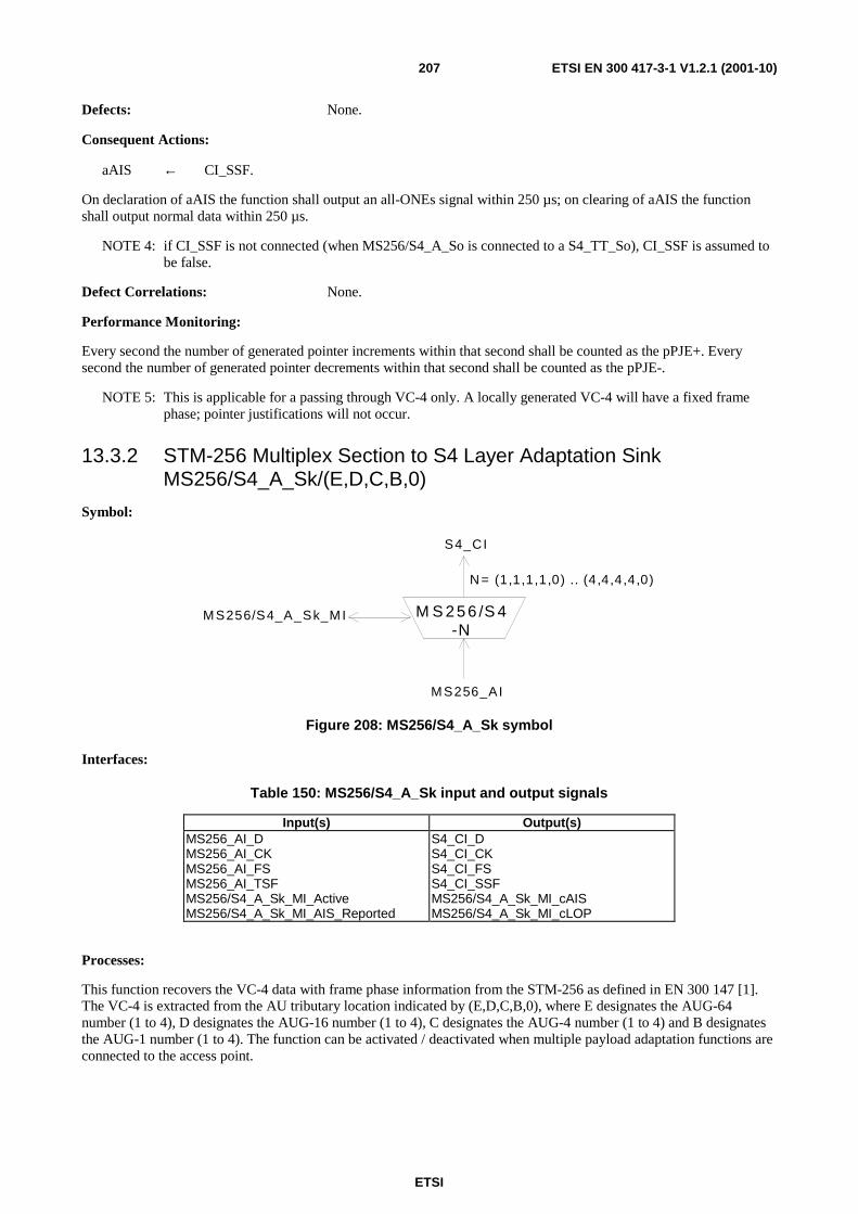
ETSI
ETSI EN 300 417-3-1 V1.2.1 (2001-10)207
Defects: None.
Consequent Actions:
aAIS ← CI_SSF.
On declaration of aAIS the function shall output an all-ONEs signal within 250 µs; on clearing of aAIS the function shall output normal data within 250 µs.
NOTE 4: if CI_SSF is not connected (when MS256/S4_A_So is connected to a S4_TT_So), CI_SSF is assumed to be false.
Defect Correlations: None.
Performance Monitoring:
Every second the number of generated pointer increments within that second shall be counted as the pPJE+. Every second the number of generated pointer decrements within that second shall be counted as the pPJE-.
NOTE 5: This is applicable for a passing through VC-4 only. A locally generated VC-4 will have a fixed frame phase; pointer justifications will not occur.
13.3.2 STM-256 Multiplex Section to S4 Layer Adaptation Sink MS256/S4_A_Sk/(E,D,C,B,0)
Symbol:
M S 256 /S 4-N
S4_CI
M S256_AI
M S256/S4_A_Sk_M I
N = (1,1,1,1,0) .. (4,4,4,4,0)
Figure 208: MS256/S4_A_Sk symbol
Interfaces:
Table 150: MS256/S4_A_Sk input and output signals
Input(s) Output(s) MS256_AI_D MS256_AI_CK MS256_AI_FS MS256_AI_TSF MS256/S4_A_Sk_MI_Active MS256/S4_A_Sk_MI_AIS_Reported
S4_CI_D S4_CI_CK S4_CI_FS S4_CI_SSF MS256/S4_A_Sk_MI_cAIS MS256/S4_A_Sk_MI_cLOP
Processes:
This function recovers the VC-4 data with frame phase information from the STM-256 as defined in EN 300 147 [1]. The VC-4 is extracted from the AU tributary location indicated by (E,D,C,B,0), where E designates the AUG-64 number (1 to 4), D designates the AUG-16 number (1 to 4), C designates the AUG-4 number (1 to 4) and B designates the AUG-1 number (1 to 4). The function can be activated / deactivated when multiple payload adaptation functions are connected to the access point.
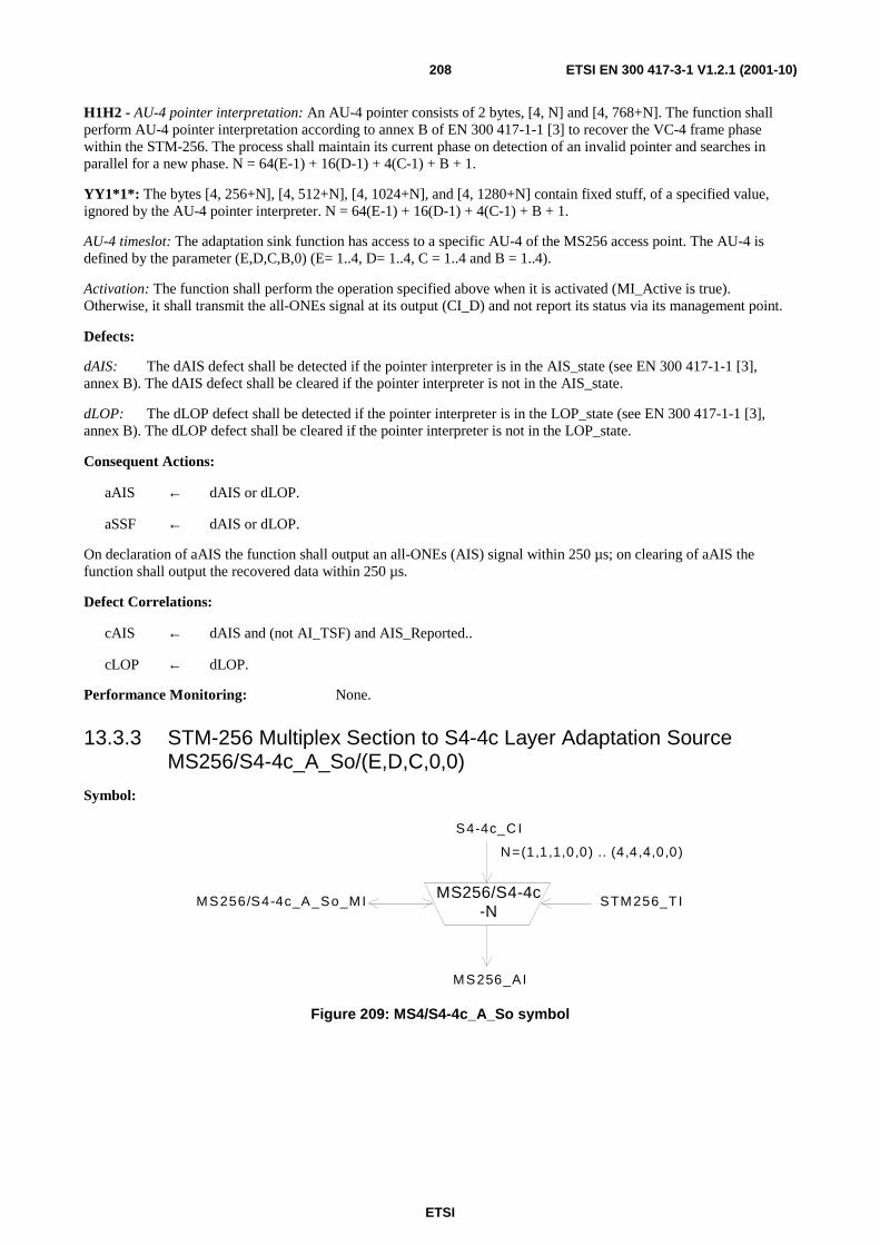
ETSI
ETSI EN 300 417-3-1 V1.2.1 (2001-10)208
H1H2 - AU-4 pointer interpretation: An AU-4 pointer consists of 2 bytes, [4, N] and [4, 768+N]. The function shall perform AU-4 pointer interpretation according to annex B of EN 300 417-1-1 [3] to recover the VC-4 frame phase within the STM-256. The process shall maintain its current phase on detection of an invalid pointer and searches in parallel for a new phase. N = 64(E-1) + 16(D-1) + 4(C-1) + B + 1.
YY1*1*: The bytes [4, 256+N], [4, 512+N], [4, 1024+N], and [4, 1280+N] contain fixed stuff, of a specified value, ignored by the AU-4 pointer interpreter. N = 64(E-1) + 16(D-1) + 4(C-1) + B + 1.
AU-4 timeslot: The adaptation sink function has access to a specific AU-4 of the MS256 access point. The AU-4 is defined by the parameter (E,D,C,B,0) (E= 1..4, D= 1..4, C = 1..4 and B = 1..4).
Activation: The function shall perform the operation specified above when it is activated (MI_Active is true). Otherwise, it shall transmit the all-ONEs signal at its output (CI_D) and not report its status via its management point.
Defects:
dAIS: The dAIS defect shall be detected if the pointer interpreter is in the AIS_state (see EN 300 417-1-1 [3], annex B). The dAIS defect shall be cleared if the pointer interpreter is not in the AIS_state.
dLOP: The dLOP defect shall be detected if the pointer interpreter is in the LOP_state (see EN 300 417-1-1 [3], annex B). The dLOP defect shall be cleared if the pointer interpreter is not in the LOP_state.
Consequent Actions:
aAIS ← dAIS or dLOP.
aSSF ← dAIS or dLOP.
On declaration of aAIS the function shall output an all-ONEs (AIS) signal within 250 µs; on clearing of aAIS the function shall output the recovered data within 250 µs.
Defect Correlations:
cAIS ← dAIS and (not AI_TSF) and AIS_Reported..
cLOP ← dLOP.
Performance Monitoring: None.
13.3.3 STM-256 Multiplex Section to S4-4c Layer Adaptation Source MS256/S4-4c_A_So/(E,D,C,0,0)
Symbol:
MS256/S4-4c-N
S4-4c_C I
M S256_AI
M S256/S4-4c_A_So_M I STM 256_TI
N=(1,1,1,0,0) .. (4,4,4,0,0)
Figure 209: MS4/S4-4c_A_So symbol
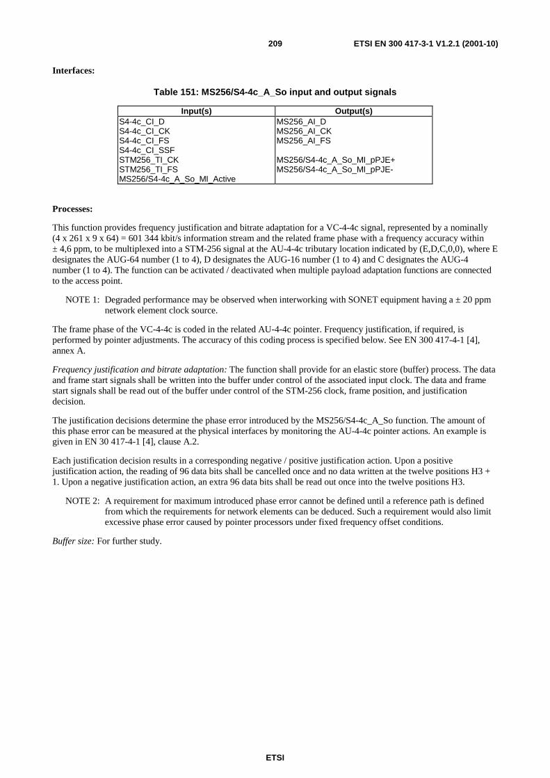
ETSI
ETSI EN 300 417-3-1 V1.2.1 (2001-10)209
Interfaces:
Table 151: MS256/S4-4c_A_So input and output signals
Input(s) Output(s) S4-4c_CI_D S4-4c_CI_CK S4-4c_CI_FS S4-4c_CI_SSF STM256_TI_CK STM256_TI_FS MS256/S4-4c_A_So_MI_Active
MS256_AI_D MS256_AI_CK MS256_AI_FS MS256/S4-4c_A_So_MI_pPJE+ MS256/S4-4c_A_So_MI_pPJE-
Processes:
This function provides frequency justification and bitrate adaptation for a VC-4-4c signal, represented by a nominally (4 x 261 x 9 x 64) = 601 344 kbit/s information stream and the related frame phase with a frequency accuracy within ± 4,6 ppm, to be multiplexed into a STM-256 signal at the AU-4-4c tributary location indicated by (E,D,C,0,0), where E designates the AUG-64 number (1 to 4), D designates the AUG-16 number (1 to 4) and C designates the AUG-4 number (1 to 4). The function can be activated / deactivated when multiple payload adaptation functions are connected to the access point.
NOTE 1: Degraded performance may be observed when interworking with SONET equipment having a ± 20 ppm network element clock source.
The frame phase of the VC-4-4c is coded in the related AU-4-4c pointer. Frequency justification, if required, is performed by pointer adjustments. The accuracy of this coding process is specified below. See EN 300 417-4-1 [4], annex A.
Frequency justification and bitrate adaptation: The function shall provide for an elastic store (buffer) process. The data and frame start signals shall be written into the buffer under control of the associated input clock. The data and frame start signals shall be read out of the buffer under control of the STM-256 clock, frame position, and justification decision.
The justification decisions determine the phase error introduced by the MS256/S4-4c_A_So function. The amount of this phase error can be measured at the physical interfaces by monitoring the AU-4-4c pointer actions. An example is given in EN 30 417-4-1 [4], clause A.2.
Each justification decision results in a corresponding negative / positive justification action. Upon a positive justification action, the reading of 96 data bits shall be cancelled once and no data written at the twelve positions H3 + 1. Upon a negative justification action, an extra 96 data bits shall be read out once into the twelve positions H3.
NOTE 2: A requirement for maximum introduced phase error cannot be defined until a reference path is defined from which the requirements for network elements can be deduced. Such a requirement would also limit excessive phase error caused by pointer processors under fixed frequency offset conditions.
Buffer size: For further study.
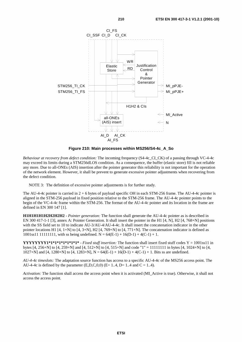
ETSI
ETSI EN 300 417-3-1 V1.2.1 (2001-10)210
ElasticStore
JustificationControl
&Pointer
Generator
STM256_TI_FS
STM256_TI_CK
WR
RD
all-ONEs(AIS) insert
CI_SSF CI_DCI_FS
CI_CK
AI_DAI_FS
AI_CK
H1H2 & CIs
MI_pPJE-
MI_pPJE+
MI_Active
N
Figure 210: Main processes within MS256/S4-4c_A_So
Behaviour at recovery from defect condition: The incoming frequency (S4-4c_CI_CK) of a passing through VC-4-4c may exceed its limits during a STM256dLOS condition. As a consequence, the buffer (elastic store) fill is not reliable any more. Due to all-ONEs (AIS) insertion after the pointer generator this reliability is not important for the operation of the network element. However, it shall be prevent to generate excessive pointer adjustments when recovering from the defect condition.
NOTE 3: The definition of excessive pointer adjustments is for further study.
The AU-4-4c pointer is carried in 2 + 6 bytes of payload specific OH in each STM-256 frame. The AU-4-4c pointer is aligned in the STM-256 payload in fixed position relative to the STM-256 frame. The AU-4-4c pointer points to the begin of the VC-4-4c frame within the STM-256. The format of the AU-4-4c pointer and its location in the frame are defined in EN 300 147 [1].
H1H1H1H1H2H2H2H2 - Pointer generation: The function shall generate the AU-4-4c pointer as is described in EN 300 417-1-1 [3], annex A: Pointer Generation. It shall insert the pointer in the H1 [4, N], H2 [4, 768+N] positions with the SS field set to 10 to indicate AU-3/AU-4/AU-4-4c. It shall insert the concatenation indicator in the other pointer locations H1 [4, 1+N] to [4, 3+N], H2 [4, 769+N] to [4, 771+N]. The concatenation indicator is defined as 1001ss11 11111111, with ss being undefined. N = 64(E-1) + 16(D-1) + 4(C-1) + 1.
YYYYYYYY1*1*1*1*1*1*1*1* - Fixed stuff insertion: The function shall insert fixed stuff codes Y = 1001ss11 in bytes [4, 256+N] to [4, 259+N] and [4, 512+N] to [4, 515+N] and code "1" = 11111111 in bytes [4, 1024+N] to [4, 1027+N] and [4, 1280+N] to [4, 1283+N], N = 64(E-1) + 16(D-1) + 4(C-1) + 1. Bits ss are undefined.
AU-4-4c timeslots: The adaptation source function has access to a specific AU-4-4c of the MS256 access point. The AU-4-4c is defined by the parameter (E,D,C,0,0) (E= 1..4, D= 1..4 and C = 1..4).
Activation: The function shall access the access point when it is activated (MI_Active is true). Otherwise, it shall not access the access point.

ETSI
ETSI EN 300 417-3-1 V1.2.1 (2001-10)211
Defects: None.
Consequent Actions:
aAIS ← CI_SSF.
On declaration of aAIS the function shall output an all-ONEs signal within 250 µs; on clearing of aAIS the function shall output normal data within 250 µs.
NOTE 4: If CI_SSF is not connected (when MS256/S4-4c_A_So is connected to a S4-4c_TT_So), CI_SSF is assumed to be false.
Defect Correlations: None.
Performance Monitoring:
Every second the number of generated pointer increments within that second shall be counted as the pPJE+. Every second the number of generated pointer decrements within that second shall be counted as the pPJE-.
NOTE 5: This is applicable for a passing through VC-4-4c only. A locally generated VC-4-4c may have a fixed frame phase; pointer justifications will not occur.
13.3.4 STM-256 Multiplex Section to S4-4c Layer Adaptation Sink MS256/S4-4c_A_Sk/(E,D,C,0,0)
Symbol:
MS256/S4-4c-N
S4-4c_C I
M S256_AI
M S256/S4-4c_A_Sk_M I
N=(1,1,1,0,0) .. (4,4,4,0,0)
Figure 211: MS256/S4-4c_A_Sk symbol
Interfaces:
Table 152: MS256/S4-4c_A_Sk input and output signals
Input(s) Output(s) MS256_AI_D MS256_AI_CK MS256_AI_FS MS256_AI_TSF MS256/S4-4c_A_Sk_MI_Active MS256/S4-4c_A_Sk_MI_AIS_Reported
S4-4c_CI_D S4-4c_CI_CK S4-4c_CI_FS S4-4c_CI_SSF MS256/S4-4c_A_Sk_MI_cAIS MS256/S4-4c_A_Sk_MI_cLOP
Processes:
This function recovers the VC-4-4c data with frame phase information from the STM-256 as defined in EN 300 147 [1]. The VC-4-4c is extracted from tributary location indicated by (E,D,C,0.0), where E designates the AUG-64 number (1 to 4), D designates the AUG-16 number (1 to 4) and C designates the AUG-4 number (1 to 4). The function can be activated / deactivated when multiple payload adaptation functions are connected to the access point.
ETSI
ETSI EN 300 417-3-1 V1.2.1 (2001-10)212
H1H1H1H1H2H2H2H2 - AU-4-4c pointer interpretation: An AU-4-4c pointer consists of 2 bytes, [4, N] and [4, 768+N]. There will be 3 concatenation indicators, each 2 bytes long, in [4, 1+N]/[4, 769+N], [4, 2+N]/[4, 770+N], and [4, 3+N]/[4, 771+N]. The function shall perform AU-4-4c pointer interpretation according to annex B of EN 300 417-1-1 [3] to recover the VC-4-4c frame phase within the STM-256. The process shall maintain its current phase on detection of an invalid pointer and searches in parallel for a new phase. N = 64(E-1) + 16(D-1) + 4(C-1) + 1.
YYYYYYYY1*1*1*1*1*1*1*1*: The bytes [4, 256+N] to [4, 259+N], [4, 512+N] to [4, 515+N], [4, 1024+N] to [4, 1027+N] and [4, 1280+N] to [4, 1283+N] contain fixed stuff, of a specified value, ignored by the AU-4-4c pointer interpreter. N = 64(E-1) + 16(D-1) + 4(C-1) + 1.
AU-4-4c timeslots: The adaptation source function has access to a specific AU-4-4c of the MS256 access point. The AU-4-4c is defined by the parameter (E,D,C,0,0) (E= 1..4, D= 1..4 and C = 1..4).
Activation: The function shall perform the operation specified above when it is activated (MI_Active is true). Otherwise, it shall transmit the all-ONEs signal at its output (CI_D) and not report its status via its management point.
Defects:
dAIS: The dAIS defect shall be detected if the pointer interpreter is in the AISX_state (see EN 300 417-1-1 [3], annex B). The dAIS defect shall be cleared if the pointer interpreter is not in the AISX_state.
dLOP: The dLOP defect shall be detected if the pointer interpreter is in the LOPX_state (see EN 300 417-1-1 [3], annex B). The dLOP defect shall be cleared if the pointer interpreter is not in the LOPX_state.
Consequent Actions:
aAIS ← dAIS or dLOP.
aSSF ← dAIS or dLOP.
On declaration of aAIS the function shall output an all-ONEs (AIS) signal within 250 µs; on clearing of aAIS the function shall output the recovered data within 250 µs.
Defect Correlations:
cAIS ← dAIS and (not aTSF) and AIS_Reported.
cLOP ← dLOP.
Performance Monitoring: None.
13.3.5 STM-256 Multiplex Section to S4-16c Layer Adaptation Source MS256/S4-16c_A_So/(E,D,0,0,0)
Symbol:
MS256/S4-16c-N
S4-16c_CI
M S256_AI
M S256/S4-16c_A_So_M I STM 256_TI
N=(1,1,0,0,0) .. (4,4,0,0,0)
Figure 212: MS256/S4-16c_A_So symbol
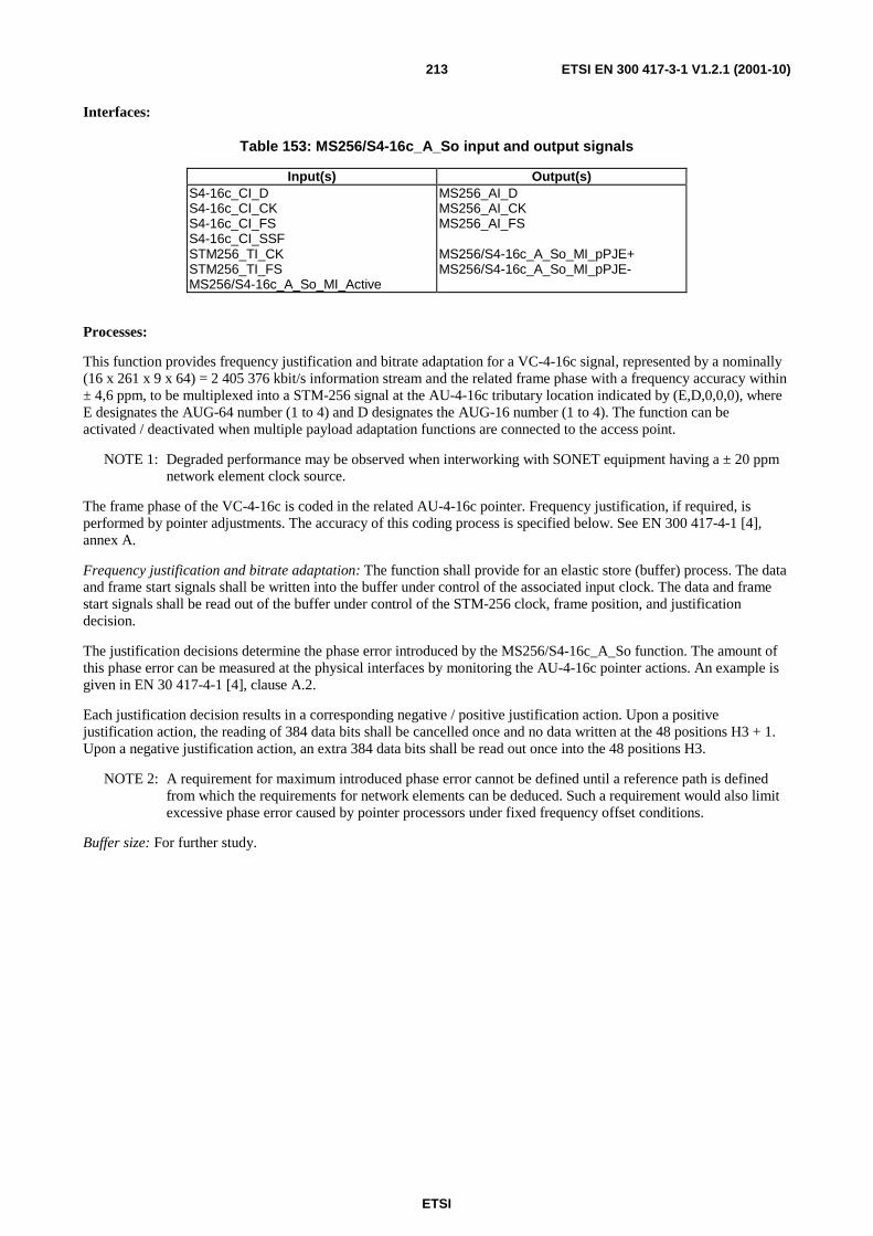
ETSI
ETSI EN 300 417-3-1 V1.2.1 (2001-10)213
Interfaces:
Table 153: MS256/S4-16c_A_So input and output signals
Input(s) Output(s) S4-16c_CI_D S4-16c_CI_CK S4-16c_CI_FS S4-16c_CI_SSF STM256_TI_CK STM256_TI_FS MS256/S4-16c_A_So_MI_Active
MS256_AI_D MS256_AI_CK MS256_AI_FS MS256/S4-16c_A_So_MI_pPJE+ MS256/S4-16c_A_So_MI_pPJE-
Processes:
This function provides frequency justification and bitrate adaptation for a VC-4-16c signal, represented by a nominally (16 x 261 x 9 x 64) = 2 405 376 kbit/s information stream and the related frame phase with a frequency accuracy within ± 4,6 ppm, to be multiplexed into a STM-256 signal at the AU-4-16c tributary location indicated by (E,D,0,0,0), where E designates the AUG-64 number (1 to 4) and D designates the AUG-16 number (1 to 4). The function can be activated / deactivated when multiple payload adaptation functions are connected to the access point.
NOTE 1: Degraded performance may be observed when interworking with SONET equipment having a ± 20 ppm network element clock source.
The frame phase of the VC-4-16c is coded in the related AU-4-16c pointer. Frequency justification, if required, is performed by pointer adjustments. The accuracy of this coding process is specified below. See EN 300 417-4-1 [4], annex A.
Frequency justification and bitrate adaptation: The function shall provide for an elastic store (buffer) process. The data and frame start signals shall be written into the buffer under control of the associated input clock. The data and frame start signals shall be read out of the buffer under control of the STM-256 clock, frame position, and justification decision.
The justification decisions determine the phase error introduced by the MS256/S4-16c_A_So function. The amount of this phase error can be measured at the physical interfaces by monitoring the AU-4-16c pointer actions. An example is given in EN 30 417-4-1 [4], clause A.2.
Each justification decision results in a corresponding negative / positive justification action. Upon a positive justification action, the reading of 384 data bits shall be cancelled once and no data written at the 48 positions H3 + 1. Upon a negative justification action, an extra 384 data bits shall be read out once into the 48 positions H3.
NOTE 2: A requirement for maximum introduced phase error cannot be defined until a reference path is defined from which the requirements for network elements can be deduced. Such a requirement would also limit excessive phase error caused by pointer processors under fixed frequency offset conditions.
Buffer size: For further study.
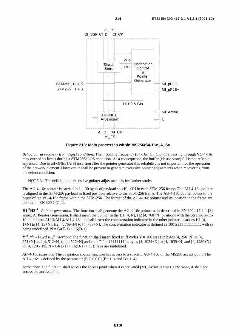
ETSI
ETSI EN 300 417-3-1 V1.2.1 (2001-10)214
ElasticStore
JustificationControl
&Pointer
GeneratorSTM256_TI_CK
WR
RD
all-ONEs(AIS) insert
CI_SSF CI_DCI_FS
CI_CK
AI_DAI_FS
AI_CK
H1H2 & CIs
MI_pPJE-
MI_pPJE+
MI_Active
N
STM256_TI_FS
Figure 213: Main processes within MS256/S4-16c_A_So
Behaviour at recovery from defect condition: The incoming frequency (S4-16c_CI_CK) of a passing through VC-4-16c may exceed its limits during a STM256dLOS condition. As a consequence, the buffer (elastic store) fill is not reliable any more. Due to all-ONEs (AIS) insertion after the pointer generator this reliability is not important for the operation of the network element. However, it shall be prevent to generate excessive pointer adjustments when recovering from the defect condition.
NOTE 3: The definition of excessive pointer adjustments is for further study.
The AU-4-16c pointer is carried in 2 + 30 bytes of payload specific OH in each STM-256 frame. The AU-4-16c pointer is aligned in the STM-256 payload in fixed position relative to the STM-256 frame. The AU-4-16c pointer points to the begin of the VC-4-16c frame within the STM-256. The format of the AU-4-16c pointer and its location in the frame are defined in EN 300 147 [1].
H116H216 - Pointer generation: The function shall generate the AU-4-16c pointer as is described in EN 300 417-1-1 [3], annex A: Pointer Generation. It shall insert the pointer in the H1 [4, N], H2 [4, 768+N] positions with the SS field set to 10 to indicate AU-3/AU-4/AU-4-16c. It shall insert the concatenation indicator in the other pointer locations H1 [4, 1+N] to [4, 15+N], H2 [4, 769+N] to [4, 783+N]. The concatenation indicator is defined as 1001ss11 11111111, with ss being undefined. N = 64(E-1) + 16(D-1).
Y321*32 - Fixed stuff insertion: The function shall insert fixed stuff codes Y = 1001ss11 in bytes [4, 256+N] to [4, 271+N] and [4, 512+N] to [4, 527+N] and code "1" = 11111111 in bytes [4, 1024+N] to [4, 1039+N] and [4, 1280+N] to [4, 1295+N], N = 64(E-1) + 16(D-1) + 1. Bits ss are undefined.
AU-4-16c timeslots: The adaptation source function has access to a specific AU-4-16c of the MS256 access point. The AU-4-16c is defined by the parameter (E,D,0,0,0) (E= 1..4 and D= 1..4).
Activation: The function shall access the access point when it is activated (MI_Active is true). Otherwise, it shall not access the access point.
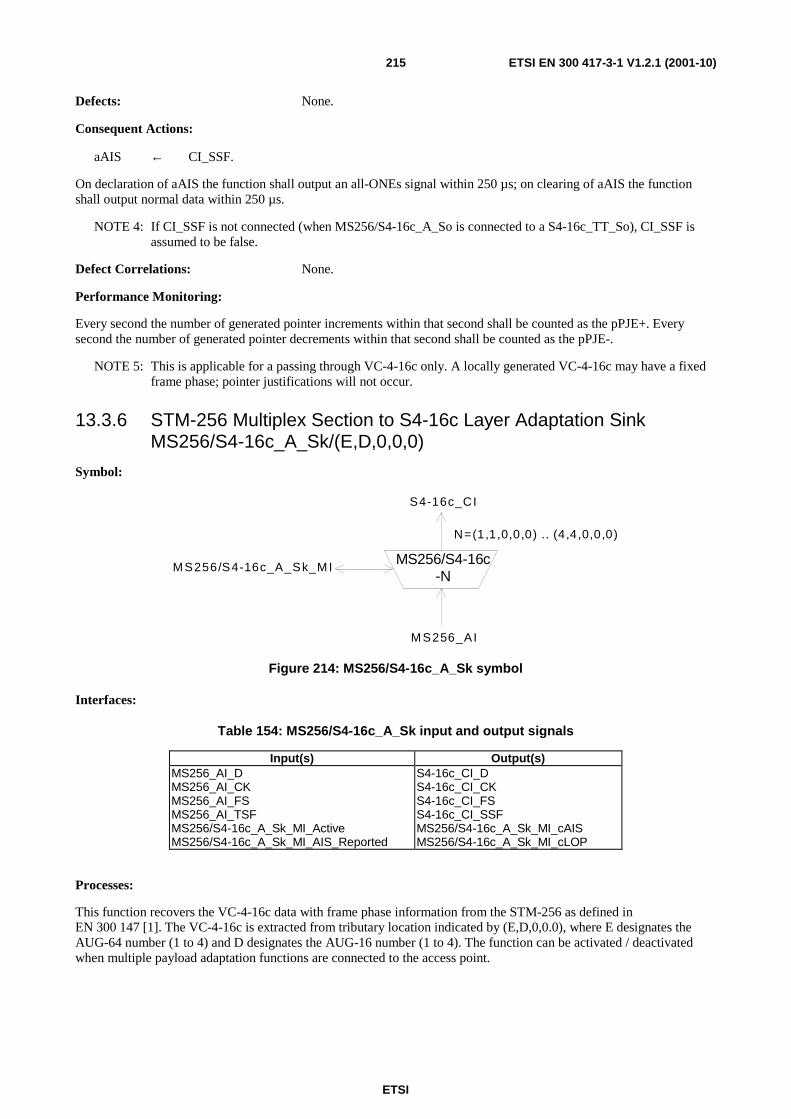
ETSI
ETSI EN 300 417-3-1 V1.2.1 (2001-10)215
Defects: None.
Consequent Actions:
aAIS ← CI_SSF.
On declaration of aAIS the function shall output an all-ONEs signal within 250 µs; on clearing of aAIS the function shall output normal data within 250 µs.
NOTE 4: If CI_SSF is not connected (when MS256/S4-16c_A_So is connected to a S4-16c_TT_So), CI_SSF is assumed to be false.
Defect Correlations: None.
Performance Monitoring:
Every second the number of generated pointer increments within that second shall be counted as the pPJE+. Every second the number of generated pointer decrements within that second shall be counted as the pPJE-.
NOTE 5: This is applicable for a passing through VC-4-16c only. A locally generated VC-4-16c may have a fixed frame phase; pointer justifications will not occur.
13.3.6 STM-256 Multiplex Section to S4-16c Layer Adaptation Sink MS256/S4-16c_A_Sk/(E,D,0,0,0)
Symbol:
MS256/S4-16c-N
S4-16c_CI
M S256_AI
M S256/S4-16c_A_Sk_M I
N=(1,1,0,0,0) .. (4,4,0,0,0)
Figure 214: MS256/S4-16c_A_Sk symbol
Interfaces:
Table 154: MS256/S4-16c_A_Sk input and output signals
Input(s) Output(s) MS256_AI_D MS256_AI_CK MS256_AI_FS MS256_AI_TSF MS256/S4-16c_A_Sk_MI_Active MS256/S4-16c_A_Sk_MI_AIS_Reported
S4-16c_CI_D S4-16c_CI_CK S4-16c_CI_FS S4-16c_CI_SSF MS256/S4-16c_A_Sk_MI_cAIS MS256/S4-16c_A_Sk_MI_cLOP
Processes:
This function recovers the VC-4-16c data with frame phase information from the STM-256 as defined in EN 300 147 [1]. The VC-4-16c is extracted from tributary location indicated by (E,D,0,0.0), where E designates the AUG-64 number (1 to 4) and D designates the AUG-16 number (1 to 4). The function can be activated / deactivated when multiple payload adaptation functions are connected to the access point.
ETSI
ETSI EN 300 417-3-1 V1.2.1 (2001-10)216
H116H216 - AU-4-16c pointer interpretation: An AU-4-16c pointer consists of 2 bytes, [4, N] and [4, 768+N]. There will be 15 concatenation indicators, each 2 bytes long, in [4, 1+N] to [4,15+N] and [4,769+N] to [4, 783+N]. The function shall perform AU-4-16c pointer interpretation according to annex B of EN 300 417-1-1 [3] to recover the VC-4-16c frame phase within the STM-256. The process shall maintain its current phase on detection of an invalid pointer and searches in parallel for a new phase. N = 64(E-1) + 16(D-1) + 4(C-1) + 1.
Y321*32: The bytes [4, 256+N] to [4, 271+N], [4, 512+N] to [4, 527+N], [4, 1024+N] to [4, 1039+N] and [4, 1280+N] to [4, 1295+N] contain fixed stuff, of a specified value, ignored by the AU-4-16c pointer interpreter, N = 64(E-1) + 16(D-1) + 4(C-1) + 1.
AU-4-16c timeslots: The adaptation source function has access to a specific AU-4-16c of the MS256 access point. The AU-4-16c is defined by the parameter (E,D,0,0,0) (E= 1..4 and D= 1..4).
Activation: The function shall perform the operation specified above when it is activated (MI_Active is true). Otherwise, it shall transmit the all-ONEs signal at its output (CI_D) and not report its status via its management point.
Defects:
dAIS: The dAIS defect shall be detected if the pointer interpreter is in the AISX_state (see EN 300 417-1-1 [3], annex B). The dAIS defect shall be cleared if the pointer interpreter is not in the AISX_state.
dLOP: The dLOP defect shall be detected if the pointer interpreter is in the LOPX_state (see EN 300 417-1-1 [3], annex B). The dLOP defect shall be cleared if the pointer interpreter is not in the LOPX_state.
Consequent Actions:
aAIS ← dAIS or dLOP.
aSSF ← dAIS or dLOP.
On declaration of aAIS the function shall output an all-ONEs (AIS) signal within 250 µs; on clearing of aAIS the function shall output the recovered data within 250 µs.
Defect Correlations:
cAIS ← dAIS and (not aTSF) and AIS_Reported.
cLOP ← dLOP.
Performance Monitoring: None.
13.3.7 STM-256 Multiplex Section to S4-64c Layer Adaptation Source MS256/S4-64c_A_So/(E,0,0,0,0)
Symbol:
MS256/S4-64c-N
S4-64c_CI
M S256_AI
M S256/S4-64c_A_So_M I STM 256_TI
N=(1,0,0,0,0) .. (4,0,0,0,0)
Figure 215: MS256/S4-64c_A_So symbol

ETSI
ETSI EN 300 417-3-1 V1.2.1 (2001-10)217
Interfaces:
Table 155: MS256/S4-64c_A_So input and output signals
Input(s) Output(s) S4-64c_CI_D S4-64c_CI_CK S4-64c_CI_FS S4-64c_CI_SSF STM256_TI_CK STM256_TI_FS MS256/S4-64c_A_So_MI_Active
MS256_AI_D MS256_AI_CK MS256_AI_FS MS256/S4-64c_A_So_MI_pPJE+ MS256/S4-64c_A_So_MI_pPJE-
Processes:
This function provides frequency justification and bitrate adaptation for a VC-4-64c signal, represented by a nominally (64 x 261 x 9 x 64) = 2 405 376 kbit/s information stream and the related frame phase with a frequency accuracy within ± 4,6 ppm, to be multiplexed into a STM-256 signal at the AU-4-64c tributary location indicated by (E,0,0,0,0), where E designates the AUG-64 number (1 to 4). The function can be activated / deactivated when multiple payload adaptation functions are connected to the access point.
NOTE 1: Degraded performance may be observed when interworking with SONET equipment having a ± 20 ppm network element clock source.
The frame phase of the VC-4-64c is coded in the related AU-4-64c pointer. Frequency justification, if required, is performed by pointer adjustments. The accuracy of this coding process is specified below. See EN 300 417-4-1 [4], annex A.
Frequency justification and bitrate adaptation: The function shall provide for an elastic store (buffer) process. The data and frame start signals shall be written into the buffer under control of the associated input clock. The data and frame start signals shall be read out of the buffer under control of the STM-256 clock, frame position, and justification decision.
The justification decisions determine the phase error introduced by the MS256/S4-64c_A_So function. The amount of this phase error can be measured at the physical interfaces by monitoring the AU-4-64c pointer actions. An example is given in EN 30 417-4-1 [4], clause A.2.
Each justification decision results in a corresponding negative / positive justification action. Upon a positive justification action, the reading of 1536 data bits shall be cancelled once and no data written at the 192 positions H3 + 1. Upon a negative justification action, an extra 1536 data bits shall be read out once into the 192 positions H3.
NOTE 2: A requirement for maximum introduced phase error cannot be defined until a reference path is defined from which the requirements for network elements can be deduced. Such a requirement would also limit excessive phase error caused by pointer processors under fixed frequency offset conditions.
Buffer size: For further study.
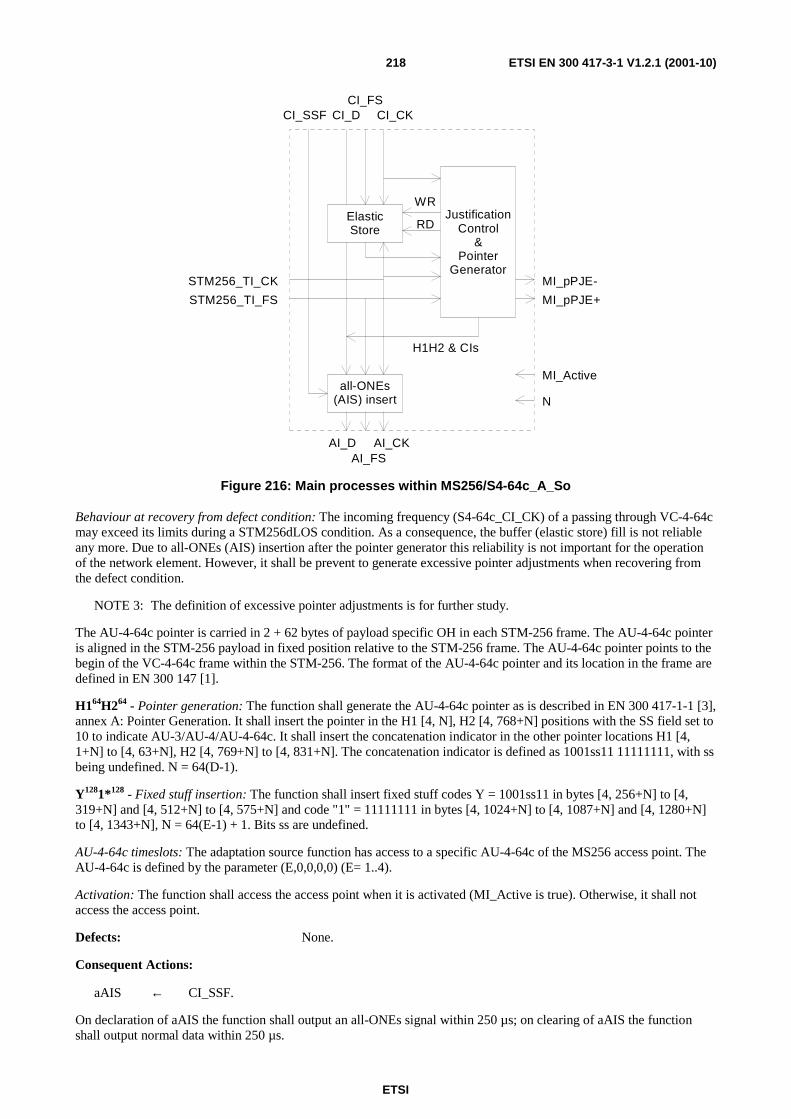
ETSI
ETSI EN 300 417-3-1 V1.2.1 (2001-10)218
ElasticStore
JustificationControl
&Pointer
Generator
STM256_TI_FS
STM256_TI_CK
WR
RD
all-ONEs(AIS) insert
CI_SSF CI_DCI_FS
CI_CK
AI_DAI_FS
AI_CK
H1H2 & CIs
MI_pPJE-
MI_pPJE+
MI_Active
N
Figure 216: Main processes within MS256/S4-64c_A_So
Behaviour at recovery from defect condition: The incoming frequency (S4-64c_CI_CK) of a passing through VC-4-64c may exceed its limits during a STM256dLOS condition. As a consequence, the buffer (elastic store) fill is not reliable any more. Due to all-ONEs (AIS) insertion after the pointer generator this reliability is not important for the operation of the network element. However, it shall be prevent to generate excessive pointer adjustments when recovering from the defect condition.
NOTE 3: The definition of excessive pointer adjustments is for further study.
The AU-4-64c pointer is carried in 2 + 62 bytes of payload specific OH in each STM-256 frame. The AU-4-64c pointer is aligned in the STM-256 payload in fixed position relative to the STM-256 frame. The AU-4-64c pointer points to the begin of the VC-4-64c frame within the STM-256. The format of the AU-4-64c pointer and its location in the frame are defined in EN 300 147 [1].
H164H264 - Pointer generation: The function shall generate the AU-4-64c pointer as is described in EN 300 417-1-1 [3], annex A: Pointer Generation. It shall insert the pointer in the H1 [4, N], H2 [4, 768+N] positions with the SS field set to 10 to indicate AU-3/AU-4/AU-4-64c. It shall insert the concatenation indicator in the other pointer locations H1 [4, 1+N] to [4, 63+N], H2 [4, 769+N] to [4, 831+N]. The concatenation indicator is defined as 1001ss11 11111111, with ss being undefined. N = 64(D-1).
Y1281*128 - Fixed stuff insertion: The function shall insert fixed stuff codes Y = 1001ss11 in bytes [4, 256+N] to [4, 319+N] and [4, 512+N] to [4, 575+N] and code "1" = 11111111 in bytes [4, 1024+N] to [4, 1087+N] and [4, 1280+N] to [4, 1343+N], N = 64(E-1) + 1. Bits ss are undefined.
AU-4-64c timeslots: The adaptation source function has access to a specific AU-4-64c of the MS256 access point. The AU-4-64c is defined by the parameter (E,0,0,0,0) (E= 1..4).
Activation: The function shall access the access point when it is activated (MI_Active is true). Otherwise, it shall not access the access point.
Defects: None.
Consequent Actions:
aAIS ← CI_SSF.
On declaration of aAIS the function shall output an all-ONEs signal within 250 µs; on clearing of aAIS the function shall output normal data within 250 µs.
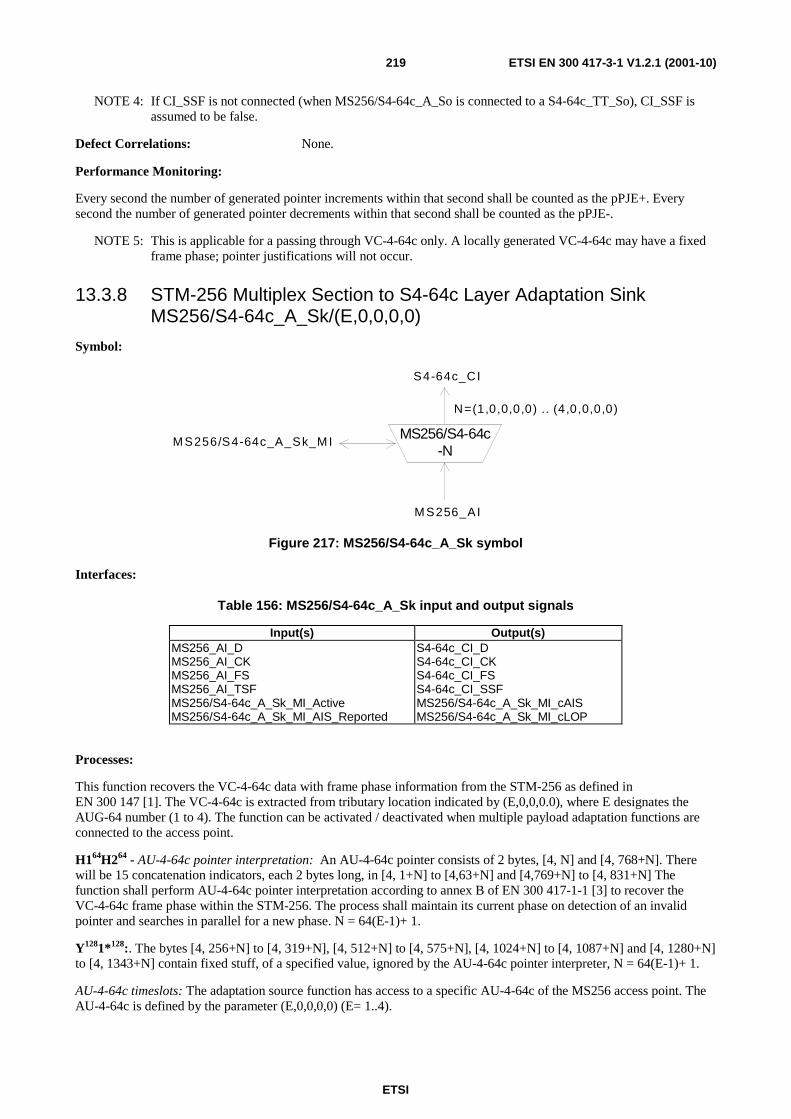
ETSI
ETSI EN 300 417-3-1 V1.2.1 (2001-10)219
NOTE 4: If CI_SSF is not connected (when MS256/S4-64c_A_So is connected to a S4-64c_TT_So), CI_SSF is assumed to be false.
Defect Correlations: None.
Performance Monitoring:
Every second the number of generated pointer increments within that second shall be counted as the pPJE+. Every second the number of generated pointer decrements within that second shall be counted as the pPJE-.
NOTE 5: This is applicable for a passing through VC-4-64c only. A locally generated VC-4-64c may have a fixed frame phase; pointer justifications will not occur.
13.3.8 STM-256 Multiplex Section to S4-64c Layer Adaptation Sink MS256/S4-64c_A_Sk/(E,0,0,0,0)
Symbol:
MS256/S4-64c-N
S4-64c_CI
M S256_AI
M S256/S4-64c_A_Sk_M I
N=(1,0,0,0,0) .. (4,0,0,0,0)
Figure 217: MS256/S4-64c_A_Sk symbol
Interfaces:
Table 156: MS256/S4-64c_A_Sk input and output signals
Input(s) Output(s) MS256_AI_D MS256_AI_CK MS256_AI_FS MS256_AI_TSF MS256/S4-64c_A_Sk_MI_Active MS256/S4-64c_A_Sk_MI_AIS_Reported
S4-64c_CI_D S4-64c_CI_CK S4-64c_CI_FS S4-64c_CI_SSF MS256/S4-64c_A_Sk_MI_cAIS MS256/S4-64c_A_Sk_MI_cLOP
Processes:
This function recovers the VC-4-64c data with frame phase information from the STM-256 as defined in EN 300 147 [1]. The VC-4-64c is extracted from tributary location indicated by (E,0,0,0.0), where E designates the AUG-64 number (1 to 4). The function can be activated / deactivated when multiple payload adaptation functions are connected to the access point.
H164H264 - AU-4-64c pointer interpretation: An AU-4-64c pointer consists of 2 bytes, [4, N] and [4, 768+N]. There will be 15 concatenation indicators, each 2 bytes long, in [4, 1+N] to [4,63+N] and [4,769+N] to [4, 831+N] The function shall perform AU-4-64c pointer interpretation according to annex B of EN 300 417-1-1 [3] to recover the VC-4-64c frame phase within the STM-256. The process shall maintain its current phase on detection of an invalid pointer and searches in parallel for a new phase. N = 64(E-1)+ 1.
Y1281*128:. The bytes [4, 256+N] to [4, 319+N], [4, 512+N] to [4, 575+N], [4, 1024+N] to [4, 1087+N] and [4, 1280+N] to [4, 1343+N] contain fixed stuff, of a specified value, ignored by the AU-4-64c pointer interpreter, N = 64(E-1)+ 1.
AU-4-64c timeslots: The adaptation source function has access to a specific AU-4-64c of the MS256 access point. The AU-4-64c is defined by the parameter (E,0,0,0,0) (E= 1..4).

ETSI
ETSI EN 300 417-3-1 V1.2.1 (2001-10)220
Activation: The function shall perform the operation specified above when it is activated (MI_Active is true). Otherwise, it shall transmit the all-ONEs signal at its output (CI_D) and not report its status via its management point.
Defects:
dAIS: The dAIS defect shall be detected if the pointer interpreter is in the AISX_state (see EN 300 417-1-1 [3], annex B). The dAIS defect shall be cleared if the pointer interpreter is not in the AISX_state.
dLOP: The dLOP defect shall be detected if the pointer interpreter is in the LOPX_state (see EN 300 417-1-1 [3], annex B). The dLOP defect shall be cleared if the pointer interpreter is not in the LOPX_state.
Consequent Actions:
aAIS ← dAIS or dLOP.
aSSF ← dAIS or dLOP.
On declaration of aAIS the function shall output an all-ONEs (AIS) signal within 250 µs; on clearing of aAIS the function shall output the recovered data within 250 µs.
Defect Correlations:
cAIS ← dAIS and (not aTSF) and AIS_Reported.
cLOP ← dLOP.
Performance Monitoring: None.
13.3.9 STM-256 Multiplex Section to S4-256c Layer Adaptation Source MS256/S4-256c_A_So
Symbol:
MS256/S4-256c
S4-256c_C I
M S256_AI
M S256/S4-256c_A_So_M I STM 256_TI
Figure 218: MS256/S4-256c_A_So symbol
Interfaces:
Table 157: MS256/S4-256c_A_So input and output signals
Input(s) Output(s) S4-256c_CI_D S4-256c_CI_CK S4-256c_CI_FS S4-256c_CI_SSF STM256_TI_CK STM256_TI_FS MS256/S4-256c_A_So_MI_Active
MS256_AI_D MS256_AI_CK MS256_AI_FS MS256/S4-256c_A_So_MI_pPJE+ MS256/S4-256c_A_So_MI_pPJE-
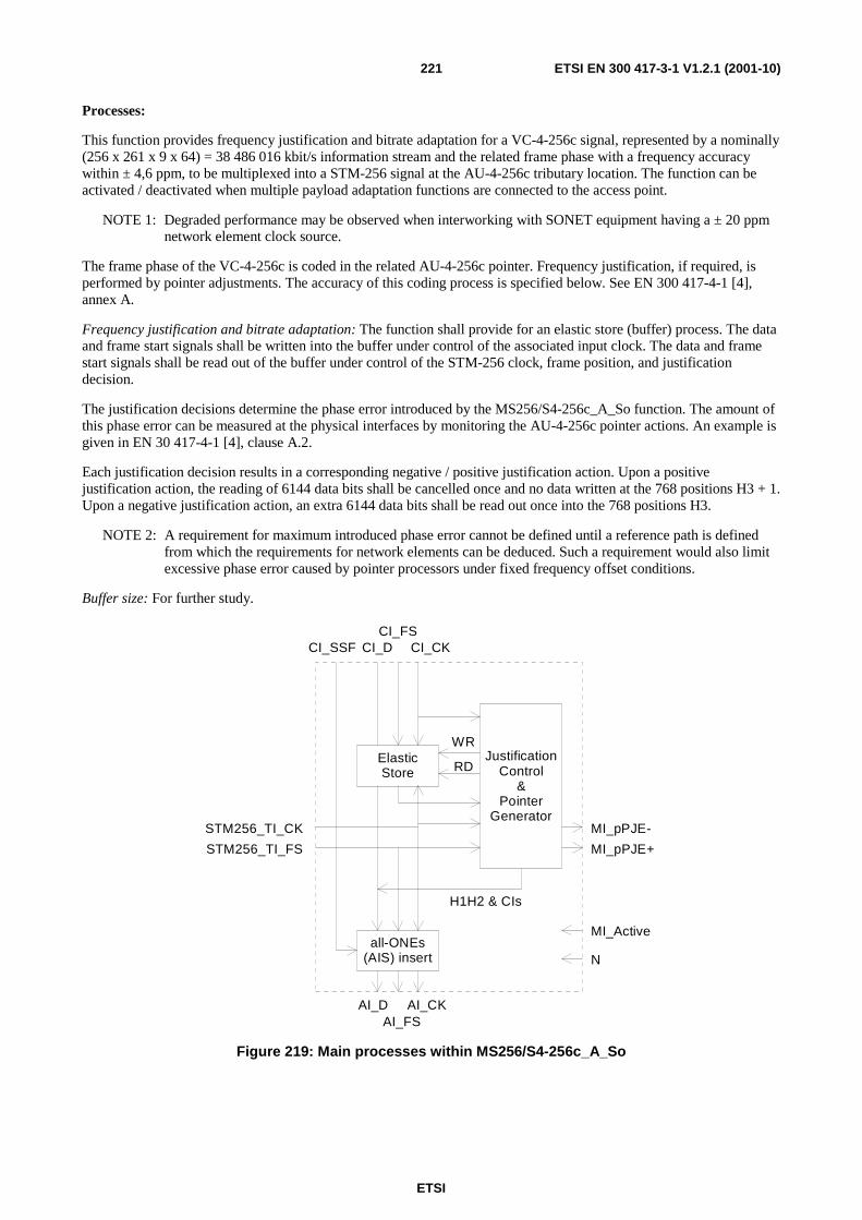
ETSI
ETSI EN 300 417-3-1 V1.2.1 (2001-10)221
Processes:
This function provides frequency justification and bitrate adaptation for a VC-4-256c signal, represented by a nominally (256 x 261 x 9 x 64) = 38 486 016 kbit/s information stream and the related frame phase with a frequency accuracy within ± 4,6 ppm, to be multiplexed into a STM-256 signal at the AU-4-256c tributary location. The function can be activated / deactivated when multiple payload adaptation functions are connected to the access point.
NOTE 1: Degraded performance may be observed when interworking with SONET equipment having a ± 20 ppm network element clock source.
The frame phase of the VC-4-256c is coded in the related AU-4-256c pointer. Frequency justification, if required, is performed by pointer adjustments. The accuracy of this coding process is specified below. See EN 300 417-4-1 [4], annex A.
Frequency justification and bitrate adaptation: The function shall provide for an elastic store (buffer) process. The data and frame start signals shall be written into the buffer under control of the associated input clock. The data and frame start signals shall be read out of the buffer under control of the STM-256 clock, frame position, and justification decision.
The justification decisions determine the phase error introduced by the MS256/S4-256c_A_So function. The amount of this phase error can be measured at the physical interfaces by monitoring the AU-4-256c pointer actions. An example is given in EN 30 417-4-1 [4], clause A.2.
Each justification decision results in a corresponding negative / positive justification action. Upon a positive justification action, the reading of 6144 data bits shall be cancelled once and no data written at the 768 positions H3 + 1. Upon a negative justification action, an extra 6144 data bits shall be read out once into the 768 positions H3.
NOTE 2: A requirement for maximum introduced phase error cannot be defined until a reference path is defined from which the requirements for network elements can be deduced. Such a requirement would also limit excessive phase error caused by pointer processors under fixed frequency offset conditions.
Buffer size: For further study.
ElasticStore
JustificationControl
&Pointer
Generator
STM256_TI_FS
STM256_TI_CK
WR
RD
all-ONEs(AIS) insert
CI_SSF CI_DCI_FS
CI_CK
AI_DAI_FS
AI_CK
H1H2 & CIs
MI_pPJE-
MI_pPJE+
MI_Active
N
Figure 219: Main processes within MS256/S4-256c_A_So
ETSI
ETSI EN 300 417-3-1 V1.2.1 (2001-10)222
Behaviour at recovery from defect condition: The incoming frequency (S4-256c_CI_CK) of a passing through VC-4-256c may exceed its limits during a STM256dLOS condition. As a consequence, the buffer (elastic store) fill is not reliable any more. Due to all-ONEs (AIS) insertion after the pointer generator this reliability is not important for the operation of the network element. However, it shall be prevent to generate excessive pointer adjustments when recovering from the defect condition.
NOTE 3: The definition of excessive pointer adjustments is for further study.
The AU-4-256c pointer is carried in 2 + 254 bytes of payload specific OH in each STM-256 frame. The AU-4-256c pointer is aligned in the STM-256 payload in fixed position relative to the STM-256 frame. The AU-4-256c pointer points to the begin of the VC-4-256c frame within the STM-256. The format of the AU-4-256c pointer and its location in the frame are defined in EN 300 147 [1].
H1256H2256 - Pointer generation: The function shall generate the AU-4-256c pointer as is described in EN 300 417-1-1 [3], annex A: Pointer Generation. It shall insert the pointer in the H1 [4, 1], H2 [4, 769] positions with the SS field set to 10 to indicate AU-3/AU-4/AU-4-256c. It shall insert the concatenation indicator in the other pointer locations H1 [4, 2] to [4, 256], H2 [4, 770] to [4, 1024]. The concatenation indicator is defined as 1001ss11 11111111, with ss being undefined.
Y5121*512 - Fixed stuff insertion: The function shall insert fixed stuff codes Y = 1001ss11 in bytes [4, 257] to [4, 768] and code "1" = 11111111 in bytes [4, 1025] to [4, 1536]. Bits ss are undefined.
Activation: The function shall access the access point when it is activated (MI_Active is true). Otherwise, it shall not access the access point.
Defects: None.
Consequent Actions:
aAIS ← CI_SSF.
On declaration of aAIS the function shall output an all-ONEs signal within 250 µs; on clearing of aAIS the function shall output normal data within 250 µs.
NOTE 4: If CI_SSF is not connected (when MS256/S4-256c_A_So is connected to a S4-256c_TT_So), CI_SSF is assumed to be false.
Defect Correlations: None.
Performance Monitoring:
Every second the number of generated pointer increments within that second shall be counted as the pPJE+. Every second the number of generated pointer decrements within that second shall be counted as the pPJE-.
NOTE 5: This is applicable for a passing through VC-4-256c only. A locally generated VC-4-256c may have a fixed frame phase; pointer justifications will not occur.
13.3.10 STM-256 Multiplex Section to S4-256c Layer Adaptation Sink MS256/S4-256c_A_Sk
Symbol:
MS256/S4-256c
S4-256c_C I
M S256_AI
M S256/S4-256c_A_Sk_M I
Figure 220: MS256/S4-256c_A_Sk symbol
ETSI
ETSI EN 300 417-3-1 V1.2.1 (2001-10)223
Interfaces:
Table 158: MS256/S4-256c_A_Sk input and output signals
Input(s) Output(s) MS256_AI_D MS256_AI_CK MS256_AI_FS MS256_AI_TSF MS256/S4-256c_A_Sk_MI_Active MS256/S4-256c_A_Sk_MI_AIS_Reported
S4-256c_CI_D S4-256c_CI_CK S4-256c_CI_FS S4-256c_CI_SSF MS256/S4-256c_A_Sk_MI_cAIS MS256/S4-256c_A_Sk_MI_cLOP
Processes:
This function recovers the VC-4-256c data with frame phase information from the STM-256 as defined in EN 300 147 [1]. The VC-4-256c is extracted from tributary location. The function can be activated / deactivated when multiple payload adaptation functions are connected to the access point.
H1256H2256 - AU-4-256c pointer interpretation: An AU-4-256c pointer consists of 2 bytes, [4, 1] and [4, 769]. There will be 256 concatenation indicators, each 2 bytes long, in [4, 2] to [4,256] and [4,770] to [4, 1024] The function shall perform AU-4-256c pointer interpretation according to annex B of EN 300 417-1-1 [3] to recover the VC-4-256c frame phase within the STM-256. The process shall maintain its current phase on detection of an invalid pointer and searches in parallel for a new phase.
Y5121*512:. The bytes [4, 257] to [4, 768] and [4, 1025] to [4, 1536] contain fixed stuff, of a specified value, ignored by the AU-4-256c pointer interpreter.
Activation: The function shall perform the operation specified above when it is activated (MI_Active is true). Otherwise, it shall transmit the all-ONEs signal at its output (CI_D) and not report its status via its management point.
Defects:
dAIS: The dAIS defect shall be detected if the pointer interpreter is in the AISX_state (see EN 300 417-1-1 [3], annex B). The dAIS defect shall be cleared if the pointer interpreter is not in the AISX_state.
dLOP: The dLOP defect shall be detected if the pointer interpreter is in the LOPX_state (see EN 300 417-1-1 [3], annex B). The dLOP defect shall be cleared if the pointer interpreter is not in the LOPX_state.
Consequent Actions:
aAIS ← dAIS or dLOP.
aSSF ← dAIS or dLOP.
On declaration of aAIS the function shall output an all-ONEs (AIS) signal within 250 µs; on clearing of aAIS the function shall output the recovered data within 250 µs.
Defect Correlations:
cAIS ← dAIS and (not aTSF) and AIS_Reported.
cLOP ← dLOP.
Performance Monitoring: None.

ETSI
ETSI EN 300 417-3-1 V1.2.1 (2001-10)224
13.3.11 STM-256 Multiplex Section to DCC Adaptation Source MS256/DCC_A_So
Symbol:
MS256/DCC
D C C_C I_D
M S256_AI
STM 256_TI
D C C _C I_CK
Figure 221: MS256/DCC_A_So symbol
Interfaces:
Table 159: MS256/DCC_A_So input and output signals
Input(s) Output(s) DCC_CI_D STM256_TI_CK STM256_TI_FS
MS256_AI_D DCC_CI_CK
Processes:
The function multiplexes the DCC CI data (576 kbit/s) into the byte locations D4 to D12 as defined in EN 300 147 [1] and depicted in figure 201.
NOTE: DCC transmission can be "disabled" when the matrix connection in the connected DCC_C function is removed.
Defects: None.
Consequent Actions: None.
Defect Correlations: None.
Performance Monitoring: None.
13.3.12 STM-256 Multiplex Section to DCC Adaptation Sink MS256/DCC_A_Sk
Symbol:
MS256/DCC
D C C _C I
M S256_AI
Figure 222: MS256/DCC_A_Sk symbol
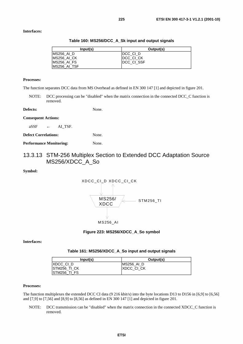
ETSI
ETSI EN 300 417-3-1 V1.2.1 (2001-10)225
Interfaces:
Table 160: MS256/DCC_A_Sk input and output signals
Input(s) Output(s) MS256_AI_D MS256_AI_CK MS256_AI_FS MS256_AI_TSF
DCC_CI_D DCC_CI_CK DCC_CI_SSF
Processes:
The function separates DCC data from MS Overhead as defined in EN 300 147 [1] and depicted in figure 201.
NOTE: DCC processing can be "disabled" when the matrix connection in the connected DCC_C function is removed.
Defects: None.
Consequent Actions:
aSSF ← AI_TSF.
Defect Correlations: None.
Performance Monitoring: None.
13.3.13 STM-256 Multiplex Section to Extended DCC Adaptation Source MS256/XDCC_A_So
Symbol:
MS256/XDCC
XD C C _C I_D
M S256_AI
STM 256_TI
XD C C _C I_C K
Figure 223: MS256/XDCC_A_So symbol
Interfaces:
Table 161: MS256/XDCC_A_So input and output signals
Input(s) Output(s) XDCC_CI_D STM256_TI_CK STM256_TI_FS
MS256_AI_D XDCC_CI_CK
Processes:
The function multiplexes the extended DCC CI data (9 216 kbit/s) into the byte locations D13 to D156 in [6,9] to [6,56] and [7,9] to [7,56] and [8,9] to [8,56] as defined in EN 300 147 [1] and depicted in figure 201.
NOTE: DCC transmission can be "disabled" when the matrix connection in the connected XDCC_C function is removed.
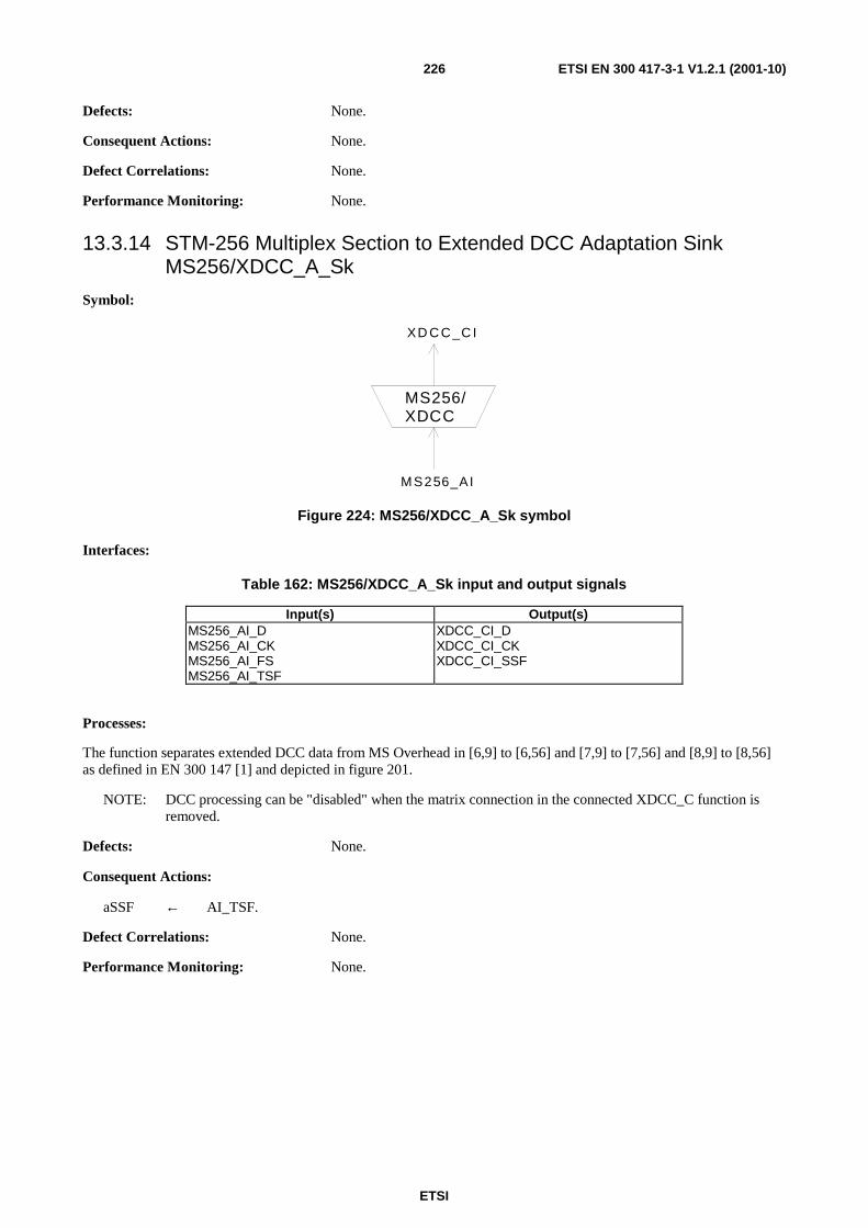
ETSI
ETSI EN 300 417-3-1 V1.2.1 (2001-10)226
Defects: None.
Consequent Actions: None.
Defect Correlations: None.
Performance Monitoring: None.
13.3.14 STM-256 Multiplex Section to Extended DCC Adaptation Sink MS256/XDCC_A_Sk
Symbol:
MS256/XDCC
XD C C _C I
M S256_AI
Figure 224: MS256/XDCC_A_Sk symbol
Interfaces:
Table 162: MS256/XDCC_A_Sk input and output signals
Input(s) Output(s) MS256_AI_D MS256_AI_CK MS256_AI_FS MS256_AI_TSF
XDCC_CI_D XDCC_CI_CK XDCC_CI_SSF
Processes:
The function separates extended DCC data from MS Overhead in [6,9] to [6,56] and [7,9] to [7,56] and [8,9] to [8,56] as defined in EN 300 147 [1] and depicted in figure 201.
NOTE: DCC processing can be "disabled" when the matrix connection in the connected XDCC_C function is removed.
Defects: None.
Consequent Actions:
aSSF ← AI_TSF.
Defect Correlations: None.
Performance Monitoring: None.
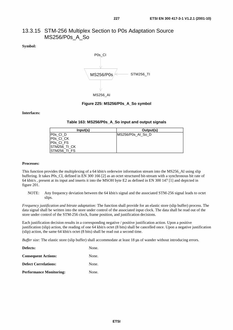
ETSI
ETSI EN 300 417-3-1 V1.2.1 (2001-10)227
13.3.15 STM-256 Multiplex Section to P0s Adaptation Source MS256/P0s_A_So
Symbol:
MS256/P0s
P0s_CI
MS256_AI
STM256_TI
Figure 225: MS256/P0s_A_So symbol
Interfaces:
Table 163: MS256/P0s_A_So input and output signals
Input(s) Output(s) P0s_CI_D P0s_CI_CK P0s_CI_FS STM256_TI_CK STM256_TI_FS
MS256/P0s_AI_So_D
Processes:
This function provides the multiplexing of a 64 kbit/s orderwire information stream into the MS256_AI using slip buffering. It takes P0s_CI, defined in EN 300 166 [2] as an octet structured bit-stream with a synchronous bit rate of 64 kbit/s , present at its input and inserts it into the MSOH byte E2 as defined in EN 300 147 [1] and depicted in figure 201.
NOTE: Any frequency deviation between the 64 kbit/s signal and the associated STM-256 signal leads to octet slips.
Frequency justification and bitrate adaptation: The function shall provide for an elastic store (slip buffer) process. The data signal shall be written into the store under control of the associated input clock. The data shall be read out of the store under control of the STM-256 clock, frame position, and justification decisions.
Each justification decision results in a corresponding negative / positive justification action. Upon a positive justification (slip) action, the reading of one 64 kbit/s octet (8 bits) shall be cancelled once. Upon a negative justification (slip) action, the same 64 kbit/s octet (8 bits) shall be read out a second time.
Buffer size: The elastic store (slip buffer) shall accommodate at least 18 µs of wander without introducing errors.
Defects: None.
Consequent Actions: None.
Defect Correlations: None.
Performance Monitoring: None.
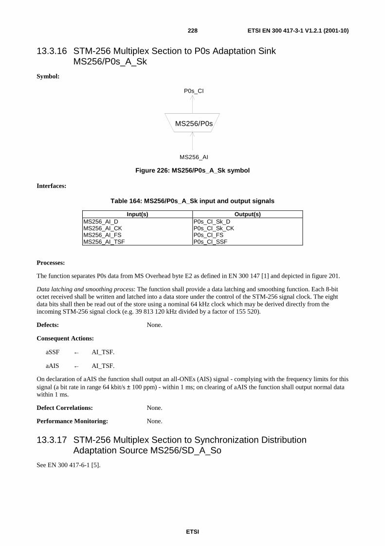
ETSI
ETSI EN 300 417-3-1 V1.2.1 (2001-10)228
13.3.16 STM-256 Multiplex Section to P0s Adaptation Sink MS256/P0s_A_Sk
Symbol:
MS256/P0s
P0s_CI
MS256_AI
Figure 226: MS256/P0s_A_Sk symbol
Interfaces:
Table 164: MS256/P0s_A_Sk input and output signals
Input(s) Output(s) MS256_AI_D MS256_AI_CK MS256_AI_FS MS256_AI_TSF
P0s_CI_Sk_D P0s_CI_Sk_CK P0s_CI_FS P0s_CI_SSF
Processes:
The function separates P0s data from MS Overhead byte E2 as defined in EN 300 147 [1] and depicted in figure 201.
Data latching and smoothing process: The function shall provide a data latching and smoothing function. Each 8-bit octet received shall be written and latched into a data store under the control of the STM-256 signal clock. The eight data bits shall then be read out of the store using a nominal 64 kHz clock which may be derived directly from the incoming STM-256 signal clock (e.g. 39 813 120 kHz divided by a factor of 155 520).
Defects: None.
Consequent Actions:
aSSF ← AI_TSF.
aAIS ← AI_TSF.
On declaration of aAIS the function shall output an all-ONEs (AIS) signal - complying with the frequency limits for this signal (a bit rate in range 64 kbit/s ± 100 ppm) - within 1 ms; on clearing of aAIS the function shall output normal data within 1 ms.
Defect Correlations: None.
Performance Monitoring: None.
13.3.17 STM-256 Multiplex Section to Synchronization Distribution Adaptation Source MS256/SD_A_So
See EN 300 417-6-1 [5].
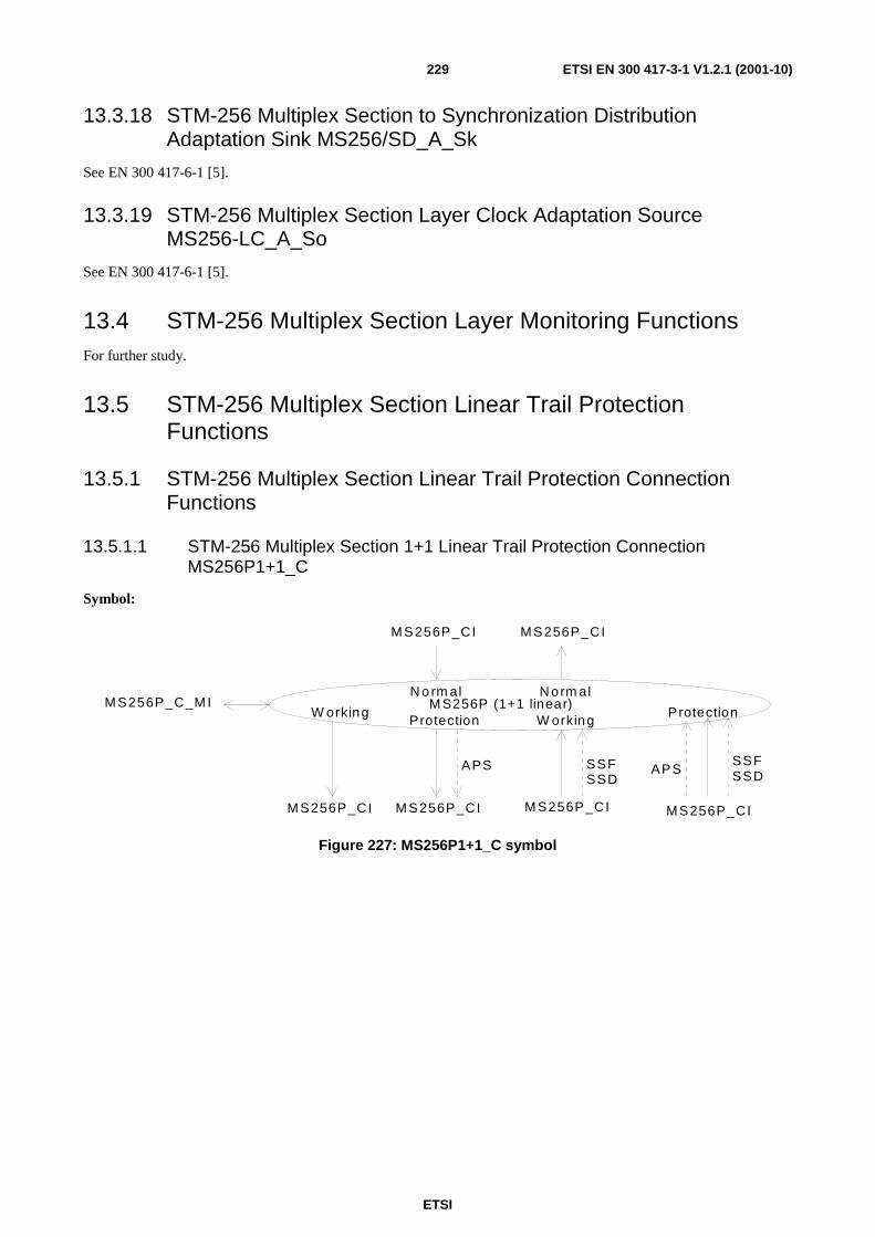
ETSI
ETSI EN 300 417-3-1 V1.2.1 (2001-10)229
13.3.18 STM-256 Multiplex Section to Synchronization Distribution Adaptation Sink MS256/SD_A_Sk
See EN 300 417-6-1 [5].
13.3.19 STM-256 Multiplex Section Layer Clock Adaptation Source MS256-LC_A_So
See EN 300 417-6-1 [5].
13.4 STM-256 Multiplex Section Layer Monitoring Functions For further study.
13.5 STM-256 Multiplex Section Linear Trail Protection Functions
13.5.1 STM-256 Multiplex Section Linear Trail Protection Connection Functions
13.5.1.1 STM-256 Multiplex Section 1+1 Linear Trail Protection Connection MS256P1+1_C
Symbol:
M S256P_CI M S256P_CI
M S256P (1+1 linear)
APS SSFSSD
W orkingProtection W orking
APSSSFSSD
Protection
M S256P_CI M S256P_CI
M S256P_CI M S256P_CI
N o rm al N orm alM S256P_C_M I
Figure 227: MS256P1+1_C symbol
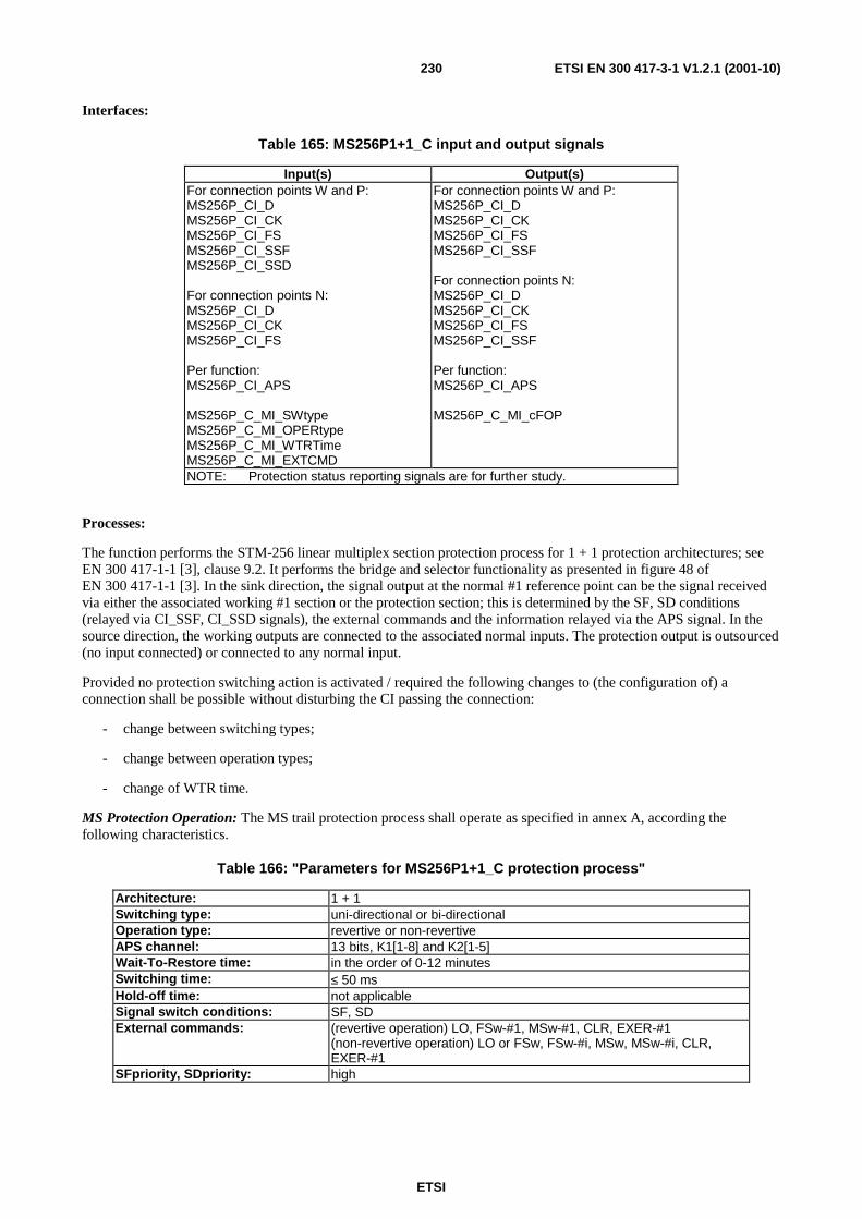
ETSI
ETSI EN 300 417-3-1 V1.2.1 (2001-10)230
Interfaces:
Table 165: MS256P1+1_C input and output signals
Input(s) Output(s) For connection points W and P: MS256P_CI_D MS256P_CI_CK MS256P_CI_FS MS256P_CI_SSF MS256P_CI_SSD For connection points N: MS256P_CI_D MS256P_CI_CK MS256P_CI_FS Per function: MS256P_CI_APS MS256P_C_MI_SWtype MS256P_C_MI_OPERtype MS256P_C_MI_WTRTime MS256P_C_MI_EXTCMD
For connection points W and P: MS256P_CI_D MS256P_CI_CK MS256P_CI_FS MS256P_CI_SSF For connection points N: MS256P_CI_D MS256P_CI_CK MS256P_CI_FS MS256P_CI_SSF Per function: MS256P_CI_APS MS256P_C_MI_cFOP
NOTE: Protection status reporting signals are for further study.
Processes:
The function performs the STM-256 linear multiplex section protection process for 1 + 1 protection architectures; see EN 300 417-1-1 [3], clause 9.2. It performs the bridge and selector functionality as presented in figure 48 of EN 300 417-1-1 [3]. In the sink direction, the signal output at the normal #1 reference point can be the signal received via either the associated working #1 section or the protection section; this is determined by the SF, SD conditions (relayed via CI_SSF, CI_SSD signals), the external commands and the information relayed via the APS signal. In the source direction, the working outputs are connected to the associated normal inputs. The protection output is outsourced (no input connected) or connected to any normal input.
Provided no protection switching action is activated / required the following changes to (the configuration of) a connection shall be possible without disturbing the CI passing the connection:
- change between switching types;
- change between operation types;
- change of WTR time.
MS Protection Operation: The MS trail protection process shall operate as specified in annex A, according the following characteristics.
Table 166: "Parameters for MS256P1+1_C protection process"
Architecture: 1 + 1 Switching type: uni-directional or bi-directional Operation type: revertive or non-revertive APS channel: 13 bits, K1[1-8] and K2[1-5] Wait-To-Restore time: in the order of 0-12 minutes Switching time: ≤ 50 ms Hold-off time: not applicable Signal switch conditions: SF, SD External commands: (revertive operation) LO, FSw-#1, MSw-#1, CLR, EXER-#1
(non-revertive operation) LO or FSw, FSw-#i, MSw, MSw-#i, CLR, EXER-#1
SFpriority, SDpriority: high
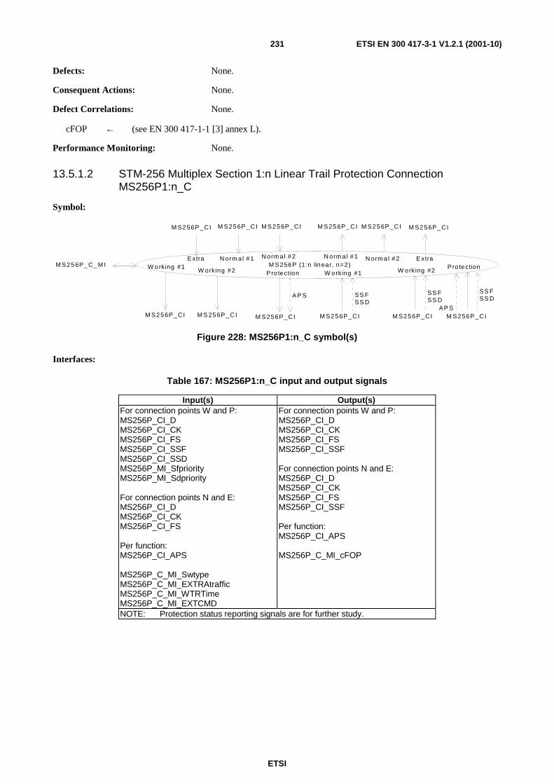
ETSI
ETSI EN 300 417-3-1 V1.2.1 (2001-10)231
Defects: None.
Consequent Actions: None.
Defect Correlations: None.
cFOP ← (see EN 300 417-1-1 [3] annex L).
Performance Monitoring: None.
13.5.1.2 STM-256 Multiplex Section 1:n Linear Trail Protection Connection MS256P1:n_C
Symbol:
M S256P_CI M S256P_CI
M S256P (1 :n linear, n=2)
AP S SS FSS D
W orking #1Pro tection W orking #1
M S 256P _C I
W ork ing #2
SS FSS D
W orking #2
AP S
SS FSS D
Protection
M S256P_CI M S256P_CI M S256P_CI
M S256P_C I M S256P_CI M S256P_CI M S256P_CI
M S256P_C_M IN orm a l #1 N orm a l #2N orm a l #1N orm a l #2
M S256P_CI
E xtra
M S256P_CI
Extra
Figure 228: MS256P1:n_C symbol(s)
Interfaces:
Table 167: MS256P1:n_C input and output signals
Input(s) Output(s) For connection points W and P: MS256P_CI_D MS256P_CI_CK MS256P_CI_FS MS256P_CI_SSF MS256P_CI_SSD MS256P_MI_Sfpriority MS256P_MI_Sdpriority For connection points N and E: MS256P_CI_D MS256P_CI_CK MS256P_CI_FS Per function: MS256P_CI_APS MS256P_C_MI_Swtype MS256P_C_MI_EXTRAtraffic MS256P_C_MI_WTRTime MS256P_C_MI_EXTCMD
For connection points W and P: MS256P_CI_D MS256P_CI_CK MS256P_CI_FS MS256P_CI_SSF For connection points N and E: MS256P_CI_D MS256P_CI_CK MS256P_CI_FS MS256P_CI_SSF Per function: MS256P_CI_APS MS256P_C_MI_cFOP
NOTE: Protection status reporting signals are for further study.

ETSI
ETSI EN 300 417-3-1 V1.2.1 (2001-10)232
Processes:
The function performs the STM-256 linear multiplex section protection process for 1:n protection architectures; see EN 300 417-1-1 [3], clause 9.2. It performs the bridge and selector functionality as presented in figure 47 of EN 300 417-1-1 [3]. In the sink direction, the signal output at the normal #i reference point can be the signal received via either the associated working #i section or the protection section; this is determined by the SF, SD conditions (relayed via CI_SSF, CI_SSD signals), the external commands and the information relayed via the APS signal. In the source direction, the working outputs are connected to the associated normal inputs. The protection output is outsourced (no input connected), connected to the extra traffic input, or connected to any normal input.
Provided no protection switching action is activated / required the following changes to (the configuration of) a connection shall be possible without disturbing the CI passing the connection:
- change between switching types;
- change of WTR time.
MS Protection Operation: The MS trail protection process shall operate as specified in annex A, according the following characteristics.
Table 168: "Parameters for MS256P1:n_C protection process"
Architecture: 1:n (n ≤ 14) Switching type: uni-directional or bi-directional Operation type: Revertive APS channel: 13 bits, K1[1-8] and K2[1-5] Wait-To-Restore time: in the order of 0-12 minutes Switching time: ≤ 50 ms Hold-off time: not applicable Signal switch conditions: SF, SD External commands: LO, FSw-#i, MSw-#i, CLR, EXER
Defects: None.
Consequent Actions:
For the case where neither the extra traffic nor a normal signal input is to be connected to the protection section output, the null signal shall be connected to the protection output. The null signal is either one of the normal signals, an all-ONEs, or a test signal.
For the case of a protection switch, the extra traffic output (if applicable) is disconnected from the protection input, set to all-ONEs (AIS) and aSSF is activated.
Defect Correlations:
cFOP ← (see EN 300 417-1-1 [3] annex L).
Performance Monitoring: None.
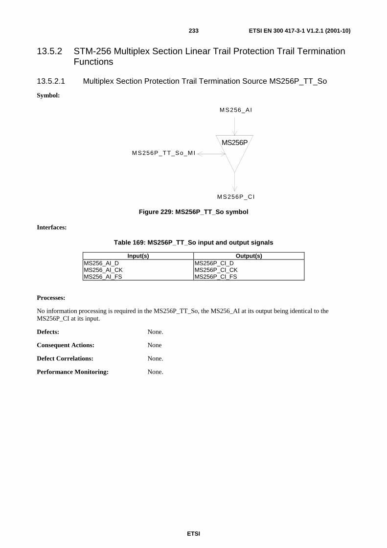
ETSI
ETSI EN 300 417-3-1 V1.2.1 (2001-10)233
13.5.2 STM-256 Multiplex Section Linear Trail Protection Trail Termination Functions
13.5.2.1 Multiplex Section Protection Trail Termination Source MS256P_TT_So
Symbol:
MS256P
M S256_AI
M S256P_CI
M S256P_TT_So_M I
Figure 229: MS256P_TT_So symbol
Interfaces:
Table 169: MS256P_TT_So input and output signals
Input(s) Output(s) MS256_AI_D MS256_AI_CK MS256_AI_FS
MS256P_CI_D MS256P_CI_CK MS256P_CI_FS
Processes:
No information processing is required in the MS256P_TT_So, the MS256_AI at its output being identical to the MS256P_CI at its input.
Defects: None.
Consequent Actions: None
Defect Correlations: None.
Performance Monitoring: None.
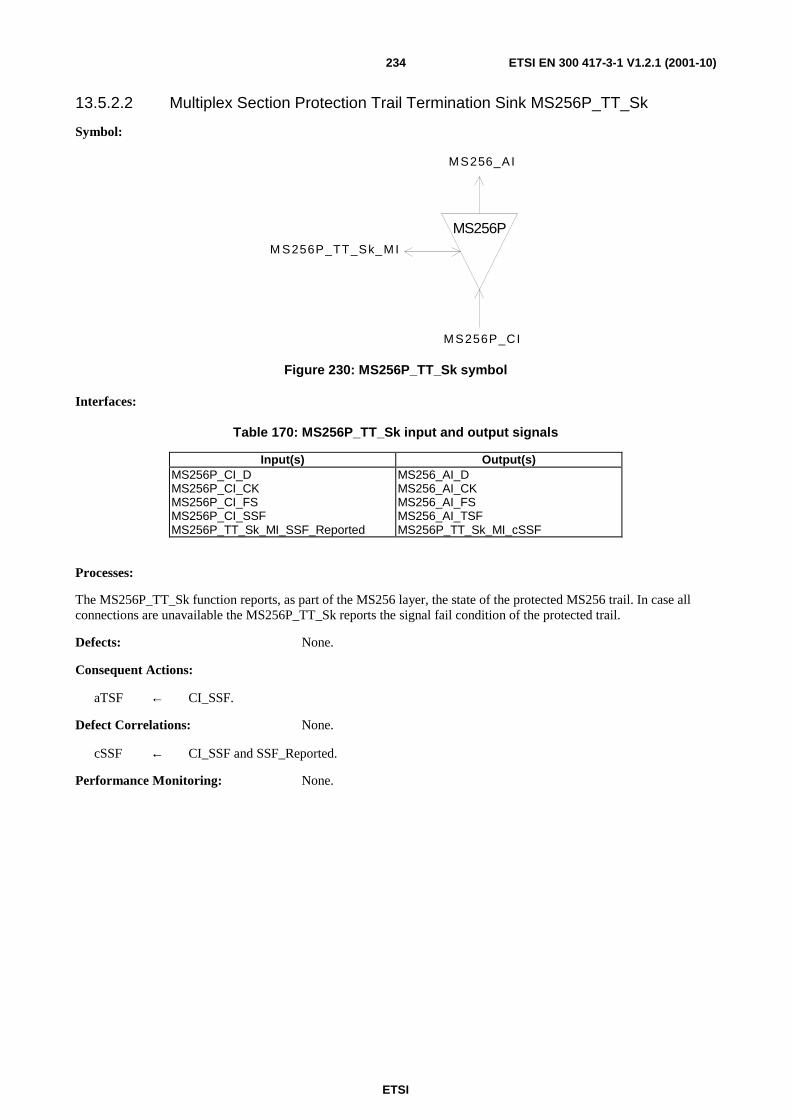
ETSI
ETSI EN 300 417-3-1 V1.2.1 (2001-10)234
13.5.2.2 Multiplex Section Protection Trail Termination Sink MS256P_TT_Sk
Symbol:
MS256P
M S256_AI
M S256P_CI
M S256P_TT_Sk_M I
Figure 230: MS256P_TT_Sk symbol
Interfaces:
Table 170: MS256P_TT_Sk input and output signals
Input(s) Output(s) MS256P_CI_D MS256P_CI_CK MS256P_CI_FS MS256P_CI_SSF MS256P_TT_Sk_MI_SSF_Reported
MS256_AI_D MS256_AI_CK MS256_AI_FS MS256_AI_TSF MS256P_TT_Sk_MI_cSSF
Processes:
The MS256P_TT_Sk function reports, as part of the MS256 layer, the state of the protected MS256 trail. In case all connections are unavailable the MS256P_TT_Sk reports the signal fail condition of the protected trail.
Defects: None.
Consequent Actions:
aTSF ← CI_SSF.
Defect Correlations: None.
cSSF ← CI_SSF and SSF_Reported.
Performance Monitoring: None.
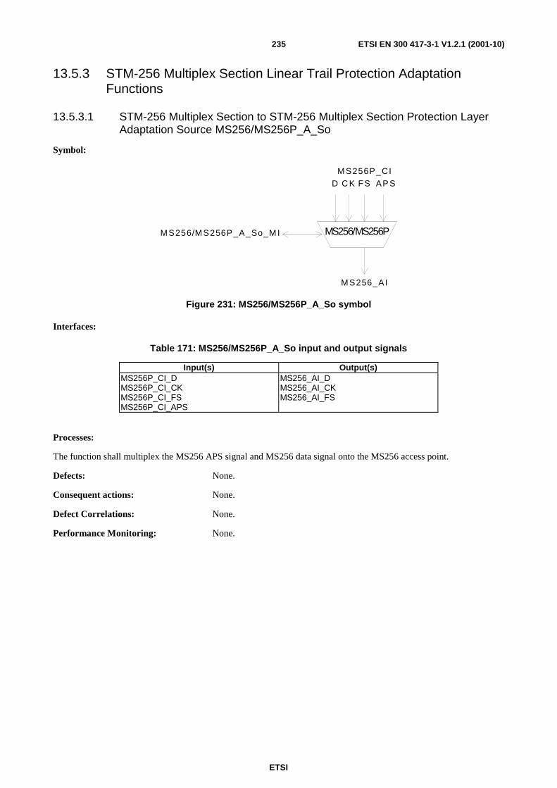
ETSI
ETSI EN 300 417-3-1 V1.2.1 (2001-10)235
13.5.3 STM-256 Multiplex Section Linear Trail Protection Adaptation Functions
13.5.3.1 STM-256 Multiplex Section to STM-256 Multiplex Section Protection Layer Adaptation Source MS256/MS256P_A_So
Symbol:
MS256/MS256P
M S256P_CI
M S256_AI
M S256/M S256P_A_So_M I
D C K FS AP S
Figure 231: MS256/MS256P_A_So symbol
Interfaces:
Table 171: MS256/MS256P_A_So input and output signals
Input(s) Output(s) MS256P_CI_D MS256P_CI_CK MS256P_CI_FS MS256P_CI_APS
MS256_AI_D MS256_AI_CK MS256_AI_FS
Processes:
The function shall multiplex the MS256 APS signal and MS256 data signal onto the MS256 access point.
Defects: None.
Consequent actions: None.
Defect Correlations: None.
Performance Monitoring: None.
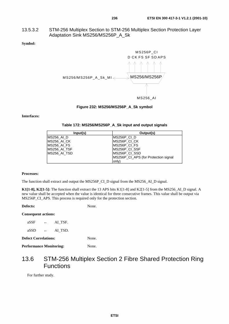
ETSI
ETSI EN 300 417-3-1 V1.2.1 (2001-10)236
13.5.3.2 STM-256 Multiplex Section to STM-256 Multiplex Section Protection Layer Adaptation Sink MS256/MS256P_A_Sk
Symbol:
MS256/MS256P
M S256P_CI
M S256_AI
M S256/M S256P_A_Sk_M I
D C K FS SF S D AP S
Figure 232: MS256/MS256P_A_Sk symbol
Interfaces:
Table 172: MS256/MS256P_A_Sk input and output signals
Input(s) Output(s) MS256_AI_D MS256_AI_CK MS256_AI_FS MS256_AI_TSF MS256_AI_TSD
MS256P_CI_D MS256P_CI_CK MS256P_CI_FS MS256P_CI_SSF MS256P_CI_SSD MS256P_CI_APS (for Protection signal only)
Processes:
The function shall extract and output the MS256P_CI_D signal from the MS256_AI_D signal.
K1[1-8], K2[1-5]: The function shall extract the 13 APS bits K1[1-8] and K2[1-5] from the MS256_AI_D signal. A new value shall be accepted when the value is identical for three consecutive frames. This value shall be output via MS256P_CI_APS. This process is required only for the protection section.
Defects: None.
Consequent actions:
aSSF ← AI_TSF.
aSSD ← AI_TSD.
Defect Correlations: None.
Performance Monitoring: None.
13.6 STM-256 Multiplex Section 2 Fibre Shared Protection Ring Functions
For further study.

ETSI
ETSI EN 300 417-3-1 V1.2.1 (2001-10)237
Annex A (normative): Generic specification of linear protection switching operation The information in this annex has been moved to EN 300 417-1-1 [3].
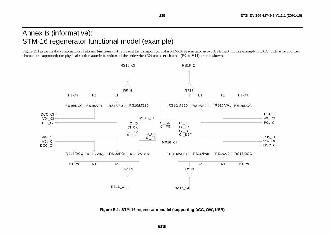
ETSI
ETSI EN 300 417-3-1 V1.2.1 (2001-10)238
Annex B (informative): STM-16 regenerator functional model (example) Figure B.1 presents the combination of atomic functions that represent the transport part of a STM-16 regenerator network element. In this example, a DCC, orderwire and user channel are supported; the physical section atomic functions of the orderwire (E0) and user channel (E0 or V11) are not shown.
RS16
RS16/MS16
RS16
RS16/MS16
MS16_CI
RS16_CI RS16_CI
RS16/V0x RS16/V0xRS16/P0s
P0s_CI
RS16/P0s
E1 E1
V0x_CI
RS16/DCC
DCC_CI
F1 D1-D3
RS16/DCC
D1-D3 F1
CI_CKCI_FS
CI_DCI_CKCI_FS
CI_SSF
RS16
RS16/MS16
RS16
RS16/MS16
MS16_CI
RS16_CIRS16_CI
RS16/V0xRS16/V0x RS16/P0s RS16/P0s
P0s_CI
E1E1
V0x_CI
RS16/DCC
F1D1-D3
RS16/DCC
DCC_CI
D1-D3F1
CI_CKCI_FS
CI_DCI_CKCI_FSCI_SSF
P0s_CIV0x_CI
DCC_CI
P0s_CIV0x_CI
DCC_CI
Figure B.1: STM-16 regenerator model (supporting DCC, OW, USR)

ETSI
ETSI EN 300 417-3-1 V1.2.1 (2001-10)239
Annex C (informative): Void
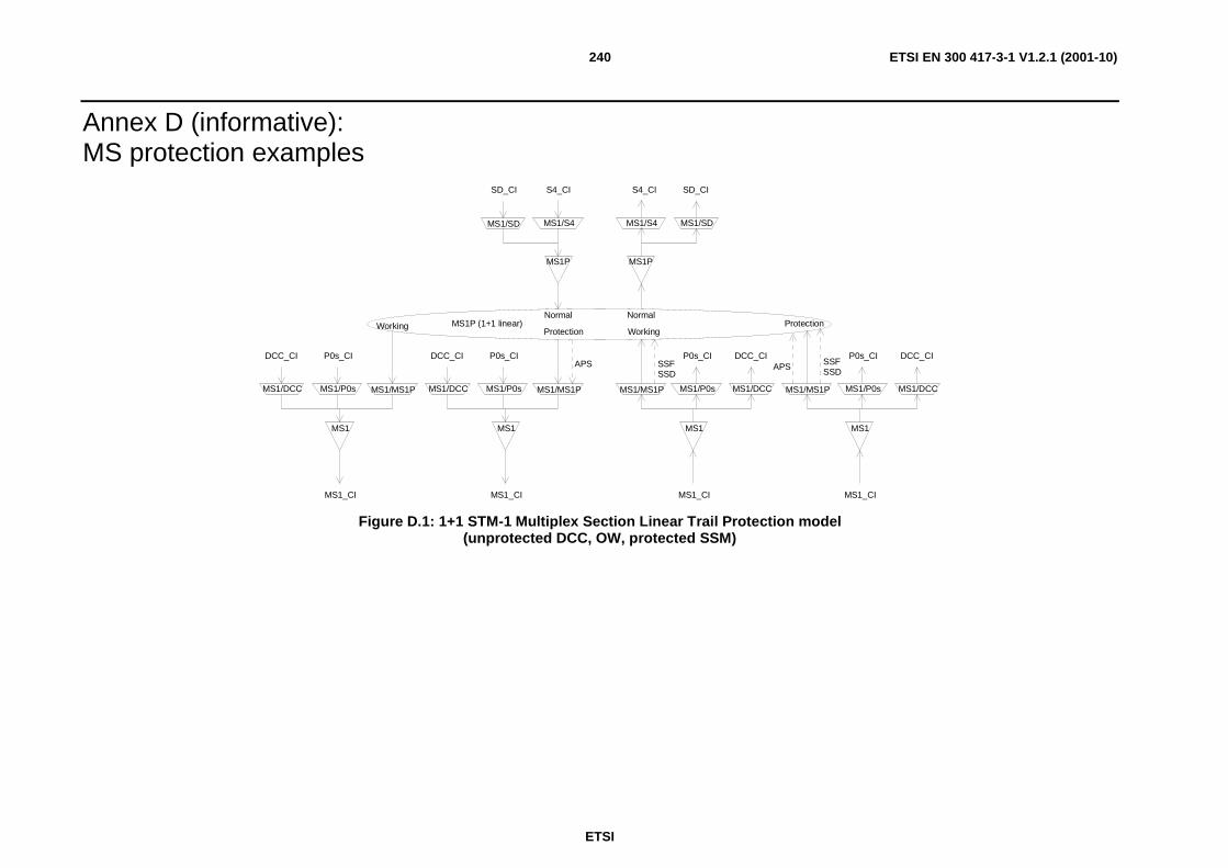
ETSI
ETSI EN 300 417-3-1 V1.2.1 (2001-10)240
Annex D (informative): MS protection examples
MS1
MS1/MS1P
MS1_CI
MS1/P0s
P0s_CI
MS1/DCC
DCC_CI
MS1
MS1/MS1P
MS1_CI
MS1/P0s
P0s_CI
MS1/DCC
DCC_CI
MS1
MS1/MS1P
MS1_CI
MS1/P0s
P0s_CI
MS1/DCC
DCC_CI
MS1
MS1/MS1P
MS1_CI
MS1/P0s
P0s_CI
MS1/DCC
DCC_CI
MS1P (1+1 linear)
APS APS SSFSSD
SSFSSD
WorkingProtection Working
Protection
MS1/S4
S4_CI
MS1/SD
SD_CI
MS1P
MS1/S4
S4_CI
MS1/SD
SD_CI
MS1P
Normal Normal
Figure D.1: 1+1 STM-1 Multiplex Section Linear Trail Protection model (unprotected DCC, OW, protected SSM)
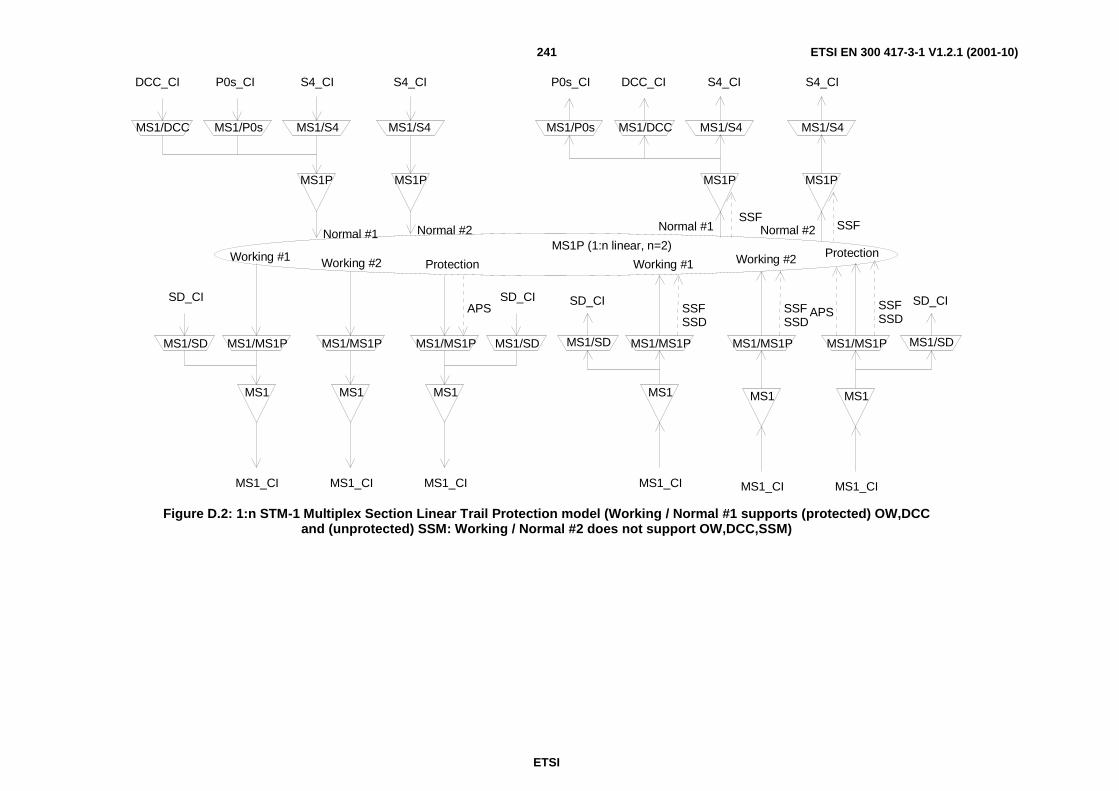
ETSI
ETSI EN 300 417-3-1 V1.2.1 (2001-10)241
MS1
MS1/MS1P
MS1_CI
MS1
MS1/MS1P
MS1_CI
MS1
MS1/MS1P
MS1_CI
MS1/P0s
P0s_CI
MS1/DCC
DCC_CI
MS1P (1:n linear, n=2)
APS SSFSSD
Working #1Protection Working #1
MS1/S4
S4_CI
MS1P
MS1/S4
S4_CI
MS1P
MS1/MS1P
MS1
MS1_CI
Working #2
MS1
MS1_CI
MS1/MS1P
SSFSSD
Working #2
MS1
MS1/MS1P
MS1_CI
APSSSFSSD
Protection
Normal #1 Normal #2
MS1/S4
S4_CI
MS1P
Normal #2
MS1/S4
S4_CI
MS1P
Normal #1SSF
SSF
MS1/SD
SD_CI
MS1/P0s
P0s_CI
MS1/DCC
DCC_CI
MS1/SD
SD_CI
MS1/SD
SD_CI
MS1/SD
SD_CI
Figure D.2: 1:n STM-1 Multiplex Section Linear Trail Protection model (Working / Normal #1 supports (protected) OW,DCC and (unprotected) SSM: Working / Normal #2 does not support OW,DCC,SSM)
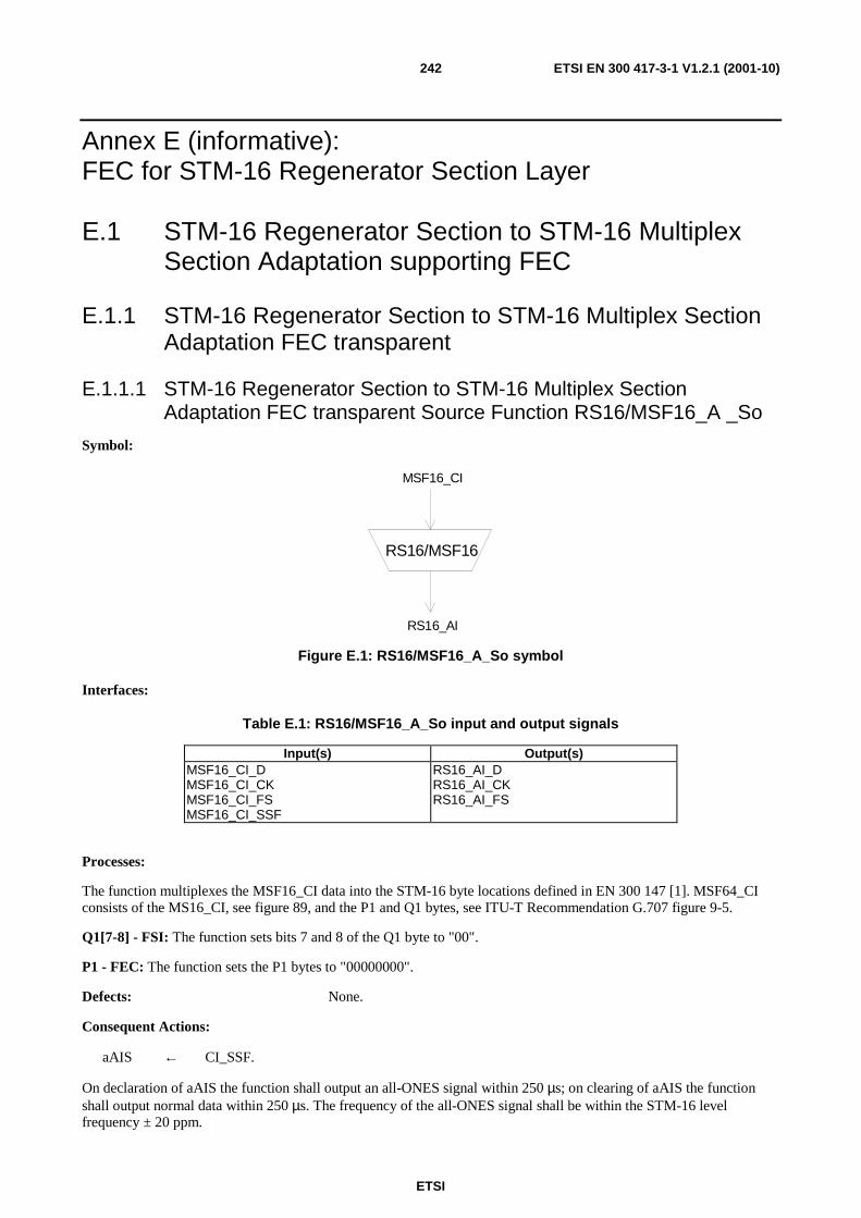
ETSI
ETSI EN 300 417-3-1 V1.2.1 (2001-10)242
Annex E (informative): FEC for STM-16 Regenerator Section Layer
E.1 STM-16 Regenerator Section to STM-16 Multiplex Section Adaptation supporting FEC
E.1.1 STM-16 Regenerator Section to STM-16 Multiplex Section Adaptation FEC transparent
E.1.1.1 STM-16 Regenerator Section to STM-16 Multiplex Section Adaptation FEC transparent Source Function RS16/MSF16_A _So
Symbol:
RS16/MSF16
MSF16_CI
RS16_AI
Figure E.1: RS16/MSF16_A_So symbol
Interfaces:
Table E.1: RS16/MSF16_A_So input and output signals
Input(s) Output(s) MSF16_CI_D MSF16_CI_CK MSF16_CI_FS MSF16_CI_SSF
RS16_AI_D RS16_AI_CK RS16_AI_FS
Processes:
The function multiplexes the MSF16_CI data into the STM-16 byte locations defined in EN 300 147 [1]. MSF64_CI consists of the MS16_CI, see figure 89, and the P1 and Q1 bytes, see ITU-T Recommendation G.707 figure 9-5.
Q1[7-8] - FSI: The function sets bits 7 and 8 of the Q1 byte to "00".
P1 - FEC: The function sets the P1 bytes to "00000000".
Defects: None.
Consequent Actions:
aAIS ← CI_SSF.
On declaration of aAIS the function shall output an all-ONES signal within 250 µs; on clearing of aAIS the function shall output normal data within 250 µs. The frequency of the all-ONES signal shall be within the STM-16 level frequency ± 20 ppm.
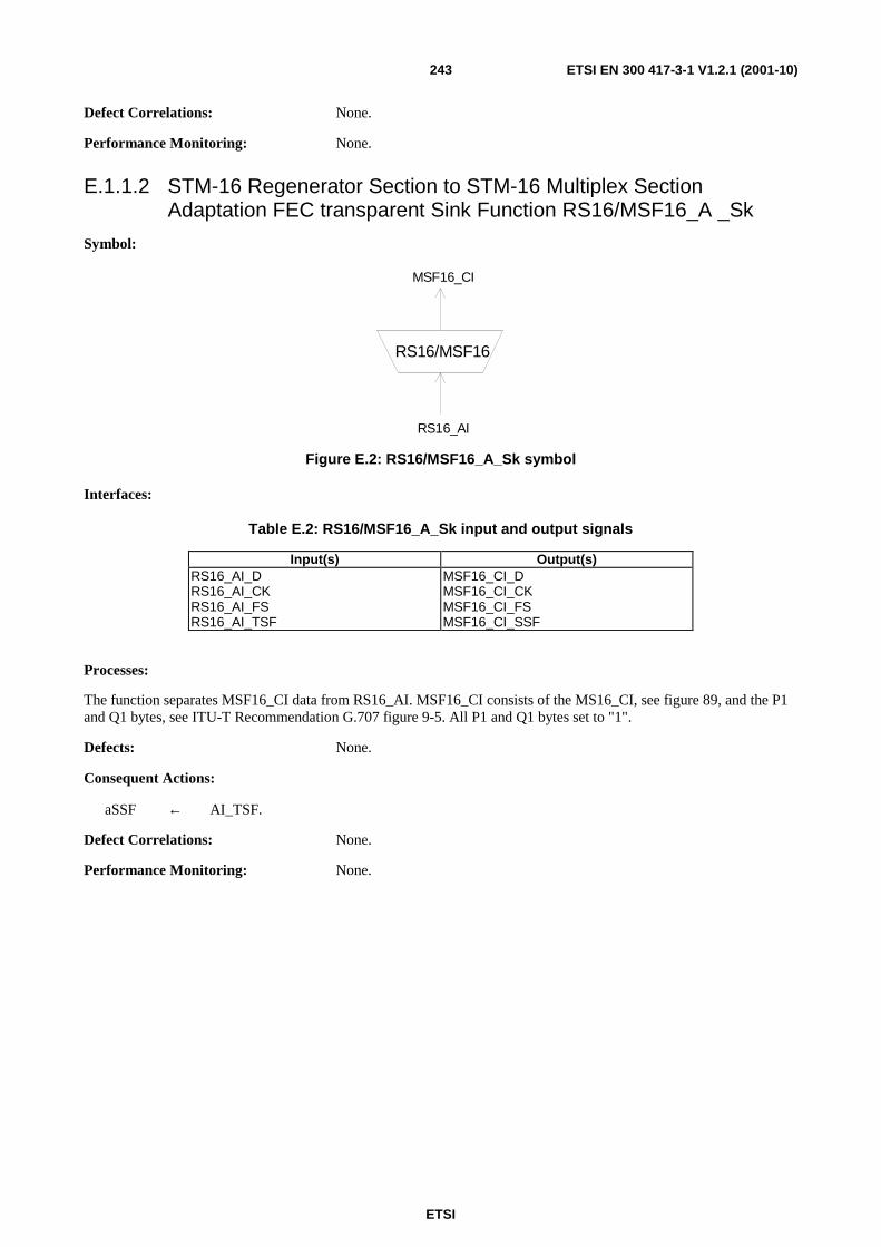
ETSI
ETSI EN 300 417-3-1 V1.2.1 (2001-10)243
Defect Correlations: None.
Performance Monitoring: None.
E.1.1.2 STM-16 Regenerator Section to STM-16 Multiplex Section Adaptation FEC transparent Sink Function RS16/MSF16_A _Sk
Symbol:
RS16/MSF16
MSF16_CI
RS16_AI
Figure E.2: RS16/MSF16_A_Sk symbol
Interfaces:
Table E.2: RS16/MSF16_A_Sk input and output signals
Input(s) Output(s) RS16_AI_D RS16_AI_CK RS16_AI_FS RS16_AI_TSF
MSF16_CI_D MSF16_CI_CK MSF16_CI_FS MSF16_CI_SSF
Processes:
The function separates MSF16_CI data from RS16_AI. MSF16_CI consists of the MS16_CI, see figure 89, and the P1 and Q1 bytes, see ITU-T Recommendation G.707 figure 9-5. All P1 and Q1 bytes set to "1".
Defects: None.
Consequent Actions:
aSSF ← AI_TSF.
Defect Correlations: None.
Performance Monitoring: None.
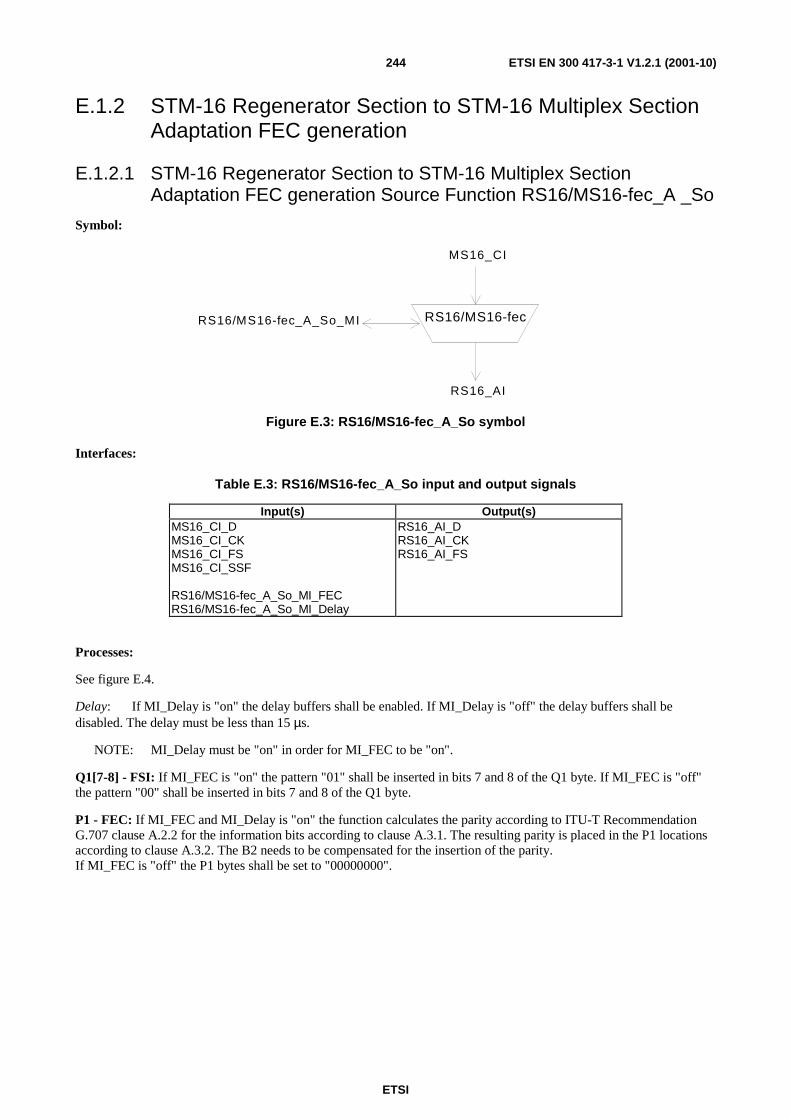
ETSI
ETSI EN 300 417-3-1 V1.2.1 (2001-10)244
E.1.2 STM-16 Regenerator Section to STM-16 Multiplex Section Adaptation FEC generation
E.1.2.1 STM-16 Regenerator Section to STM-16 Multiplex Section Adaptation FEC generation Source Function RS16/MS16-fec_A _So
Symbol:
RS16/MS16-fec
MS16_CI
RS16_AI
RS16/MS16-fec_A_So_MI
Figure E.3: RS16/MS16-fec_A_So symbol
Interfaces:
Table E.3: RS16/MS16-fec_A_So input and output signals
Input(s) Output(s) MS16_CI_D MS16_CI_CK MS16_CI_FS MS16_CI_SSF RS16/MS16-fec_A_So_MI_FEC RS16/MS16-fec_A_So_MI_Delay
RS16_AI_D RS16_AI_CK RS16_AI_FS
Processes:
See figure E.4.
Delay: If MI_Delay is "on" the delay buffers shall be enabled. If MI_Delay is "off" the delay buffers shall be disabled. The delay must be less than 15 µs.
NOTE: MI_Delay must be "on" in order for MI_FEC to be "on".
Q1[7-8] - FSI: If MI_FEC is "on" the pattern "01" shall be inserted in bits 7 and 8 of the Q1 byte. If MI_FEC is "off" the pattern "00" shall be inserted in bits 7 and 8 of the Q1 byte.
P1 - FEC: If MI_FEC and MI_Delay is "on" the function calculates the parity according to ITU-T Recommendation G.707 clause A.2.2 for the information bits according to clause A.3.1. The resulting parity is placed in the P1 locations according to clause A.3.2. The B2 needs to be compensated for the insertion of the parity. If MI_FEC is "off" the P1 bytes shall be set to "00000000".
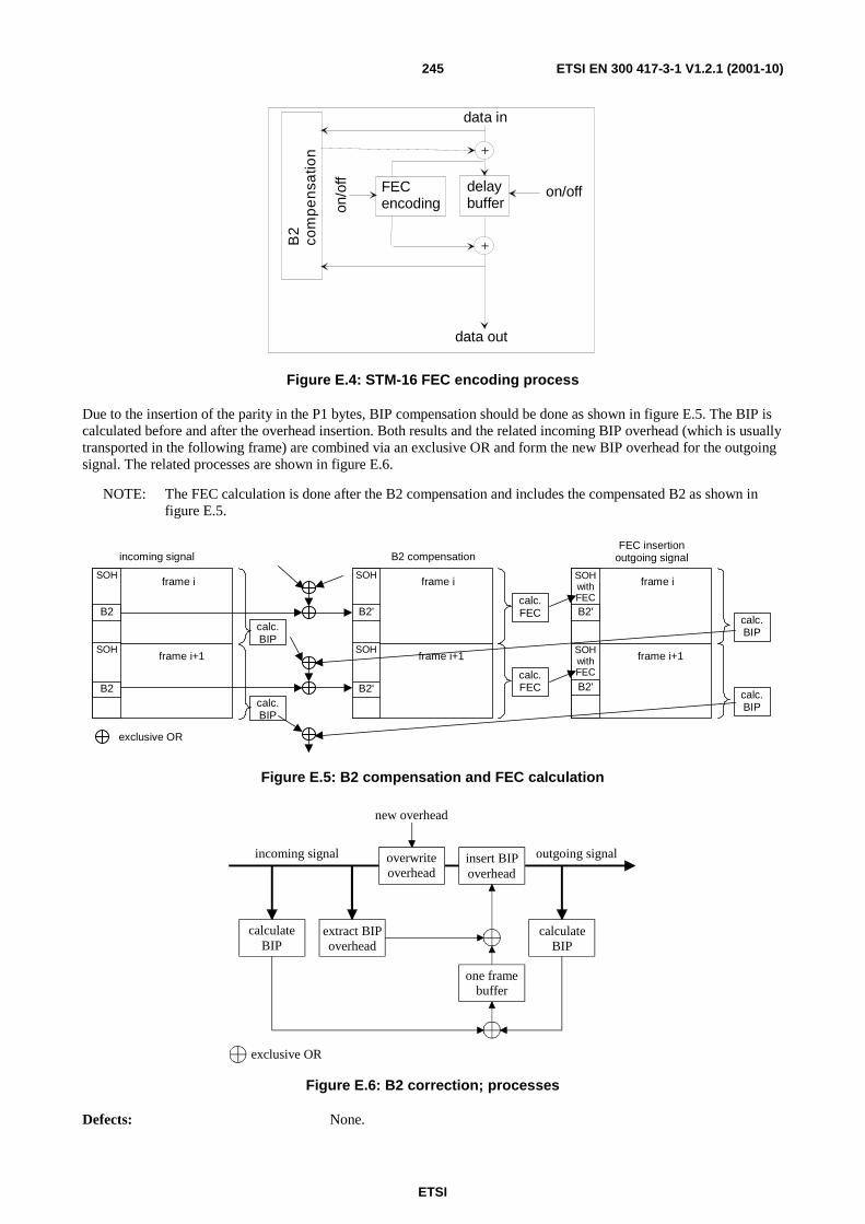
ETSI
ETSI EN 300 417-3-1 V1.2.1 (2001-10)245
data in
delaybuffer
FECencoding
B2
com
pe
nsa
tion
data out
on/off
on/o
ff
+
+
Figure E.4: STM-16 FEC encoding process
Due to the insertion of the parity in the P1 bytes, BIP compensation should be done as shown in figure E.5. The BIP is calculated before and after the overhead insertion. Both results and the related incoming BIP overhead (which is usually transported in the following frame) are combined via an exclusive OR and form the new BIP overhead for the outgoing signal. The related processes are shown in figure E.6.
NOTE: The FEC calculation is done after the B2 compensation and includes the compensated B2 as shown in figure E.5.
frame i
frame i+1
calc.BIP
frame i
frame i+1
calc.FEC
incoming signal B2 compensation
exclusive OR
SOH SOH
B2 B2'
frame i
frame i+1
calc.BIP
FEC insertionoutgoing signal
SOHwithFEC
SOHwithFECB2'
B2'calc.FEC
SOH
calc.BIP
calc.BIP
B2
SOH
B2'
Figure E.5: B2 compensation and FEC calculation
new overhead
incoming signal outgoing signal
exclusive OR
overwrite overhead
insert BIP overhead
calculate BIP
extract BIP overhead
calculate BIP
one frame buffer
Figure E.6: B2 correction; processes
Defects: None.
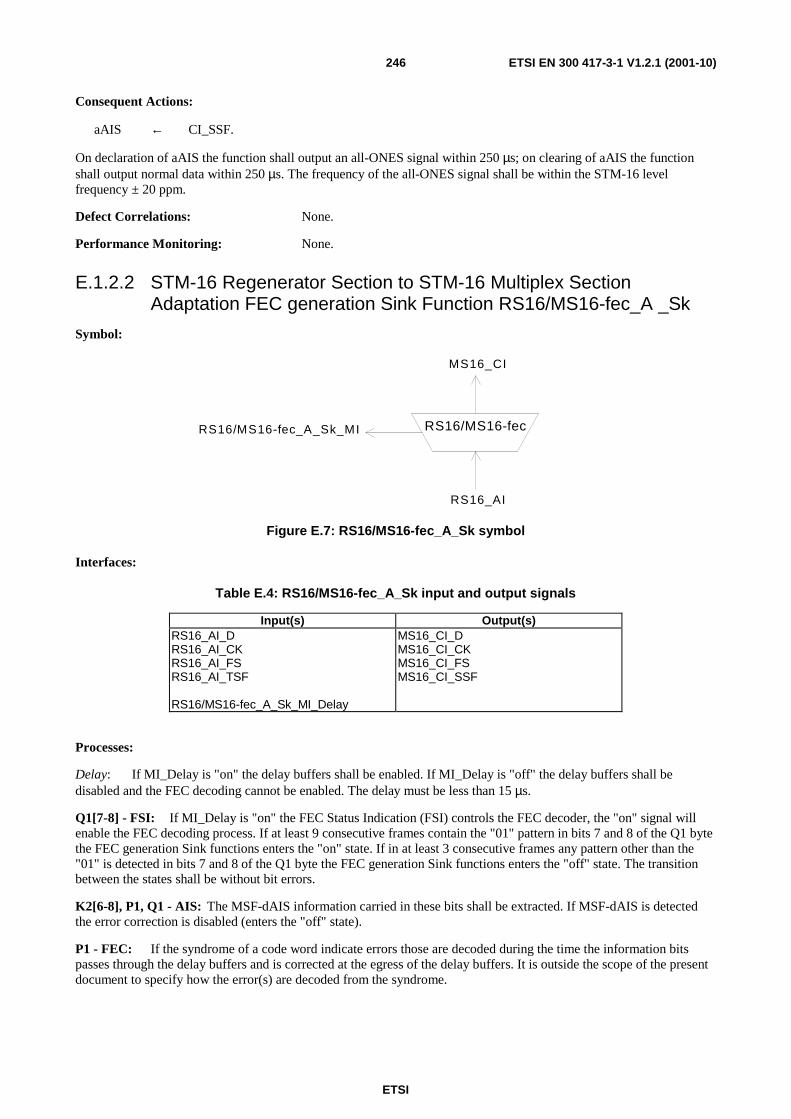
ETSI
ETSI EN 300 417-3-1 V1.2.1 (2001-10)246
Consequent Actions:
aAIS ← CI_SSF.
On declaration of aAIS the function shall output an all-ONES signal within 250 µs; on clearing of aAIS the function shall output normal data within 250 µs. The frequency of the all-ONES signal shall be within the STM-16 level frequency ± 20 ppm.
Defect Correlations: None.
Performance Monitoring: None.
E.1.2.2 STM-16 Regenerator Section to STM-16 Multiplex Section Adaptation FEC generation Sink Function RS16/MS16-fec_A _Sk
Symbol:
RS16/MS16-fec
MS16_CI
RS16_AI
RS16/MS16-fec_A_Sk_MI
Figure E.7: RS16/MS16-fec_A_Sk symbol
Interfaces:
Table E.4: RS16/MS16-fec_A_Sk input and output signals
Input(s) Output(s) RS16_AI_D RS16_AI_CK RS16_AI_FS RS16_AI_TSF RS16/MS16-fec_A_Sk_MI_Delay
MS16_CI_D MS16_CI_CK MS16_CI_FS MS16_CI_SSF
Processes:
Delay: If MI_Delay is "on" the delay buffers shall be enabled. If MI_Delay is "off" the delay buffers shall be disabled and the FEC decoding cannot be enabled. The delay must be less than 15 µs.
Q1[7-8] - FSI: If MI_Delay is "on" the FEC Status Indication (FSI) controls the FEC decoder, the "on" signal will enable the FEC decoding process. If at least 9 consecutive frames contain the "01" pattern in bits 7 and 8 of the Q1 byte the FEC generation Sink functions enters the "on" state. If in at least 3 consecutive frames any pattern other than the "01" is detected in bits 7 and 8 of the Q1 byte the FEC generation Sink functions enters the "off" state. The transition between the states shall be without bit errors.
K2[6-8], P1, Q1 - AIS: The MSF-dAIS information carried in these bits shall be extracted. If MSF-dAIS is detected the error correction is disabled (enters the "off" state).
P1 - FEC: If the syndrome of a code word indicate errors those are decoded during the time the information bits passes through the delay buffers and is corrected at the egress of the delay buffers. It is outside the scope of the present document to specify how the error(s) are decoded from the syndrome.

ETSI
ETSI EN 300 417-3-1 V1.2.1 (2001-10)247
data in
data out
on/off
disable
AIS detection
FEC decoding
delay buffers
Figure E.8: STM-16 FEC decoding process
Defects:
dAIS: If at least x consecutive frames contain the "111" pattern in bits 6, 7 and 8 of the K2 byte and the "11111111" pattern in the P1 and Q1 bytes a dAIS defect shall be detected. dAIS shall be cleared if in at least x consecutive frames any pattern other then the "111" is detected in bits 6, 7 and 8 of byte K2 or the "11111111" pattern in P1 byte or Q1 byte. The x shall be in range 3 to 5.
dDEG: For further study.
Consequent Actions:
aSSF ← AI_TSF.
disable error correction ← dAIS.
Defect Correlations: None.
Performance Monitoring: None.
ETSI
ETSI EN 300 417-3-1 V1.2.1 (2001-10)248
Annex F (informative): Bibliography
• ETSI TS 101 009 (V.1.1): "Transmission and Multiplexing (TM); Synchronous Digital Hierarchy (SDH); Network protection schemes; Types and characteristics".
• ITU-T Recommendation G.707: "Network Node Interface for the Synchronous digital hierarchy (SDH)".
• ITU-T Recommendation G.783: "Characteristics of synchronous digital hierarchy (SDH) equipment functional blocks".
ETSI
ETSI EN 300 417-3-1 V1.2.1 (2001-10)249
History
Document history
Edition 1 June 1997 Publication as ETS 300 417-3-1
V1.1.2 November 1998 Publication
V1.1.3 May 1999 Publication
V1.2.1 June 2001 One-step Approval Procedure OAP 20011012: 2001-06-13 to 2001-10-12
V1.2.1 October 2001 Publication