Embed Size (px)
Citation preview

3-D integrated heterogeneous intra-chipfree-space optical interconnect
Berkehan Ciftcioglu,1 Rebecca Berman,2 Shang Wang,1 Jianyun Hu,1Ioannis Savidis,1 Manish Jain,2 Duncan Moore,2 Michael Huang,1
Eby G. Friedman,1 Gary Wicks,2 and Hui Wu1,∗
1Department of Electrical and Computer Engineering, University of Rochester,Rochester, New York 14627, USA
2Institute of Optics, University of Rochester, Rochester, New York 14627, USA*[email protected]
Abstract: This paper presents the first chip-scale demonstration of anintra-chip free-space optical interconnect (FSOI) we recently proposed.This interconnect system provides point-to-point free-space optical linksbetween any two communication nodes, and hence constructs an all-to-allintra-chip communication fabric, which can be extended for inter-chip com-munications as well. Unlike electrical and other waveguide-based opticalinterconnects, FSOI exhibits low latency, high energy efficiency, and largebandwidth density, and hence can significantly improve the performance offuture many-core chips. In this paper, we evaluate the performance of theproposed FSOI interconnect, and compare it to a waveguide-based opticalinterconnect with wavelength division multiplexing (WDM). It shows thatthe FSOI system can achieve significantly lower loss and higher energyefficiency than the WDM system, even with optimistic assumptions for thelatter. A 1×1-cm2 chip prototype is fabricated on a germanium substratewith integrated photodetectors. Commercial 850-nm GaAs vertical-cavity-surface-emitting-lasers (VCSELs) and fabricated fused silica microlensesare 3-D integrated on top of the substrate. At 1.4-cm distance, the measuredoptical transmission loss is 5 dB, the crosstalk is less than -20 dB, and theelectrical-to-electrical bandwidth is 3.3 GHz. The latter is mainly limitedby the 5-GHz VCSEL.
© 2012 Optical Society of America
OCIS codes: (130.3120) Integrated optics devices; (220.0220) Optical design and fabrication;(200.2605) Free-space optical communications; (250.5300) Photonic integrated circuits.
References and links1. J. W. Goodman, F. J. Leonberger, S. -Y. Kung, and R. A. Athale, “Optical interconnections for VLSI systems,”
Proc. IEEE 72(7), 850–866 (1984).2. D. A. B. Miller, “Optical interconnects to silicon,” IEEE J. Sel. Top. Quantum Electron. 6(6), 1312–1317 (2000).3. L. Schares, J. A. Kash, F. E. Doany, C. L. Schow, C. Schuster, D. M. Kuchta, P. K. Pepeljugoski, J. M. Trewhella,
C. W. Baks, R. A. John, L. Shan, Y. H. Kwark, R. A. Budd, P. Chiniwalla, F. R. Libsch, J. Rosner, C. K. Tsang,C. S. Patel, J. D. Schaub, R. Dangel, F. Horst, B. J. Offrein, D. Kucharski, D. Guckenberger, S. Hegde, H. Nyikal,C. -K. Lin; A. Tandon, G. R. Trott, M. Nystrom, D. P. Bour, M. R. T. Tan, and D. W. Dolfi (IBM T.J. WatsonResearch Center), “Terabus: terabit/second-class card-level optical interconnect technologies,” IEEE J. Sel. Top.Quantum Electron. 12(5), 1032–1044 (2006).
4. I. Young, E. Mohammed, J. Liao, A. Kern, S. Palermo, B. Block, M. Reshotko, and P. Chang, “Optical I/Otechnology for tera-scale computing,” IEEE Int. Solid-State Circuits Conf. 468–469 (2009).
#159376 - $15.00 USD Received 8 Dec 2011; revised 29 Jan 2012; accepted 30 Jan 2012; published 7 Feb 2012(C) 2012 OSA 13 February 2012 / Vol. 20, No. 4 / OPTICS EXPRESS 4331
5. R. G. Beausoleil, J. Ahn, N. Binkert, A. Davis, D. Fattal, M. Fiorentino, N. P. Jouppi, M. McLaren, C. M.Santori, R. S. Schreiber, S. M. Spillane, D. Vantrease, and Q. Xu, (HP Labs, Palo Alto, CA), “A nanophotonicinterconnect for high-performance many-core computation,” 16th IEEE Symp. High Performance Interconnects,HOTI ’08 182–189 (2008).
6. D. V. Plant, M. B. Venditti, E. Laprise, J. Faucher, K. Razavi, M. Chteauneuf, A. G. Kirk, and J. S. Ahearn,“256-channel bidirectional optical interconnect using VCSELs and photodiodes on CMOS,” IEEE J. LigthwaveTechnol. 19(8), 1093–1103 (2001).
7. J. Jahns, “Planar packaging of free-space optical interconnections”, Proc. IEEE 82(11), 769–779 (1994).8. M. W. Haney, M. P. Christensen, P. Milojkovic, G. J. Fokken, M. Vickberg, B. K. Gilbert, J. Rieve, J. Ekman, P.
Chandramani, and F. Kiamilev, (George Mason Univ., Fairfax, VA), “Description and evaluation of the FAST-Netsmart pixel-based optical interconnection prototype,” Proc. IEEE 88(6), 819–828 (2000).
9. H. Thienpont, C. Debaes, V. Baukens, H. Ottevaere, P. Vynck, P. Tuteleers, G. Verschaffelt, B. Volckaerts, A.Hermanne, and M. Hanney (Vrije Univ., Brussels), “Plastic microoptical interconnection modules for parallelfree-space inter- and intra-MCM data communication,” Proc. IEEE 88(6), 769–779 (2000).
10. C. Debaes, M. Vervaeke, V. Baukens, H. Ottevaere, P. Vynck, P. Tuteleers, B. Volckaerts, W. Meeus, M. Brunfaut,J. Van Campenhout, A. Hermanne, and H. Thienpont, “Low-cost microoptical modules for MCM level opticalinterconnections,” IEEE J. Sel. Top. Quantum Electron. 9(2), 518–530 (2003).
11. M. J. McFadden, M. Iqbal, T. Dillon, R. Nair, T. Gu, D. W. Prather, and M. W. Haney, “Multiscale free-space op-tics interconnects for intrachip global communication: motivation, analysis, and experimental validation,” Appl.Opt. 45(25), 6358–6366 (2006).
12. B. Ciftcioglu, R. Berman, J. Zhang, Z. Darling, S. Wang, J. Hu, J. Xue, A. Garg, M. Jain, I. Savidis, D. Moore,M. Huang, E. G. Friedman, G. Wicks, and Hui Wu, “A 3-D integrated intra-chip free-space optical interconnectfor many-core chips,” IEEE Photon. Technol. Lett. 23(3), 164–166 (2011).
13. J. Xue, A. Garg, B. Ciftcioglu, Jianyun Hu, S. Wang I. Savidis, M. Jain, R. Berman, P. Liu, M. Huang, H. Wu,E. Friedman, G. Wicks, D. Moore, “An intra-chip free-space optical interconnect,” 37th Int. Symp. ComputerArchitecture ISCA 94–105 (2010).
14. D. Louderback, O. Sjolund, E. R. Hegblom, S. Nakagawa, J. Ko, and L. A. Coldren, “Modulation and free-spacelink characteristics of monolithically integrated vertical-cavity lasers and photodetectors with microlenses,” IEEEJ. Sel. Top. Quantum Electron. 5(2), 155–165 (1999).
15. Y. -C. Chang and L. A. Coldren, “Optimization of VCSEL structure for high-speed operation,” IEEE 21st Int.Semiconductor Laser Conf., ISLC 159–160 (2008).
16. P. Dong, S. Liao, D. Feng, H. Liang, D. Zheng, R. Shafiiha, C. -C. Kung, W. Qian, G. Li, X. Zheng, A. V. Krish-namoorthy, and M. Asghari, “Low Vpp, ultralow-energy, compact, high-speed silicon electro-optic modulator,”Opt. Express 17(25), 22484–22490 (2009).
17. J. Cardenas, C. B. Poitras, J. T. Robinson, K. Preston, L. Chen, and M. Lipson, “Low loss etchless siliconphotonic waveguides,” Opt. Express 17(6), 4752–4757 (2009).
18. “International Technology Roadmap of Semiconductors,” www.itrs.net. (2009).19. Q. Xu, S. Manipatruni, B. Schmidt, J. Shakya, and M. Lipson, “12.5 Gbit/s carrier-injection-based silicon mi-
croring silicon modulators,” Opt. Express 15(2), 430–436 (2007).20. B. Ciftcioglu, J. Zhang, R. Sobolewski, and H. Wu, “An 850-nm normal-incidence germanium metal-
semiconductor-metal photodetector with 13-GHz bandwidth and 8-µA dark current,” IEEE Photon. Technol.Lett. 22(24), 1851–1853 (2010).
21. F. T. O’Neill and J. T. Sheridan, “Photoresist reflow method of microlens production part I: background andexperiments,” Optik 113(9), 391–404 (2002).
1. Introduction
The performance of microprocessors continues to improve with technology scaling, especiallythrough the increase of the number of cores. Communications within these chips, e.g. betweenprocessor cores and at the memory/processor interface, will demand larger bandwidth density,smaller latency and better signal integrity. To meet these demands, conventional electrical inter-connects need better materials to minimize transmission loss, and increased circuit complexity(e.g. equalization) to achieve larger bandwidth, both of which increase energy consumption.Therefore, a fundamental change is required for the inter- and intra-chip interconnects. Op-tical interconnect exhibits inherent advantages in loss, delay and bandwidth compared to itselectrical counterpart, and can potentially lead to significant performance gains and energysavings [1,2]. For inter-chip communications, optical interconnects with point-to-point topolo-gies have already been developed, typically using on-board waveguides and directly modulatedlasers [3, 4].
#159376 - $15.00 USD Received 8 Dec 2011; revised 29 Jan 2012; accepted 30 Jan 2012; published 7 Feb 2012(C) 2012 OSA 13 February 2012 / Vol. 20, No. 4 / OPTICS EXPRESS 4332
For intra-chip communications, however, optical interconnect schemes previously proposedcreate new challenges: packet-switching optical interconnects require either all-optical switch-ing, which is still difficult for silicon, or repeated electrooptic and optoelectronic conver-sions, which largely defeats optical interconnect’s advantages in latency and energy efficiency.Circuit-switching optical interconnect needs wavelength division multiplexing (WDM) to sat-isfy the bandwidth density requirement. WDM, however, requires precise optical filters (e.g.microrings) with accurate wavelength control and minimal transmission loss [5], which are dif-ficult to fabricate in large-scale chips and consume significantly more power if thermal tuning isneeded. In addition, all of these waveguide-based systems use an power-hungry external laseras the optical power supply, which is difficult to integrate and of high cost, especially in theWDM case.
As an alternative, free-space optics can be used to overcome some of the technical challengesof waveguide-based systems. Free-space optics has been successfully applied in board-to-board[6,7] and inter-chip applications [8–11]. These earlier proposals use arrays of discrete vertical-cavity surface emitting lasers (VCSELs) and photodetectors (PDs), and interconnect them usingfree-space optics. In [7], diffractive mirrors and fused silica slabs were used to guide lightbeams. Due to the small diffraction angle of the mirrors, a large number of reflections arerequired within the silica slab, resulting in a long optical path even for a short distance. In [6,8], lenses with large aperture size and focal length are shared among multiple VCSELs andphotodetector arrays to increase bandwidth density. However, these macro-scale lenses are toothick to be fabricated using standard microfabrication processes, and the long throw distanceresults in a large link latency. Improved designs using microlenses [10, 11] has been proposedto overcome these limitations.
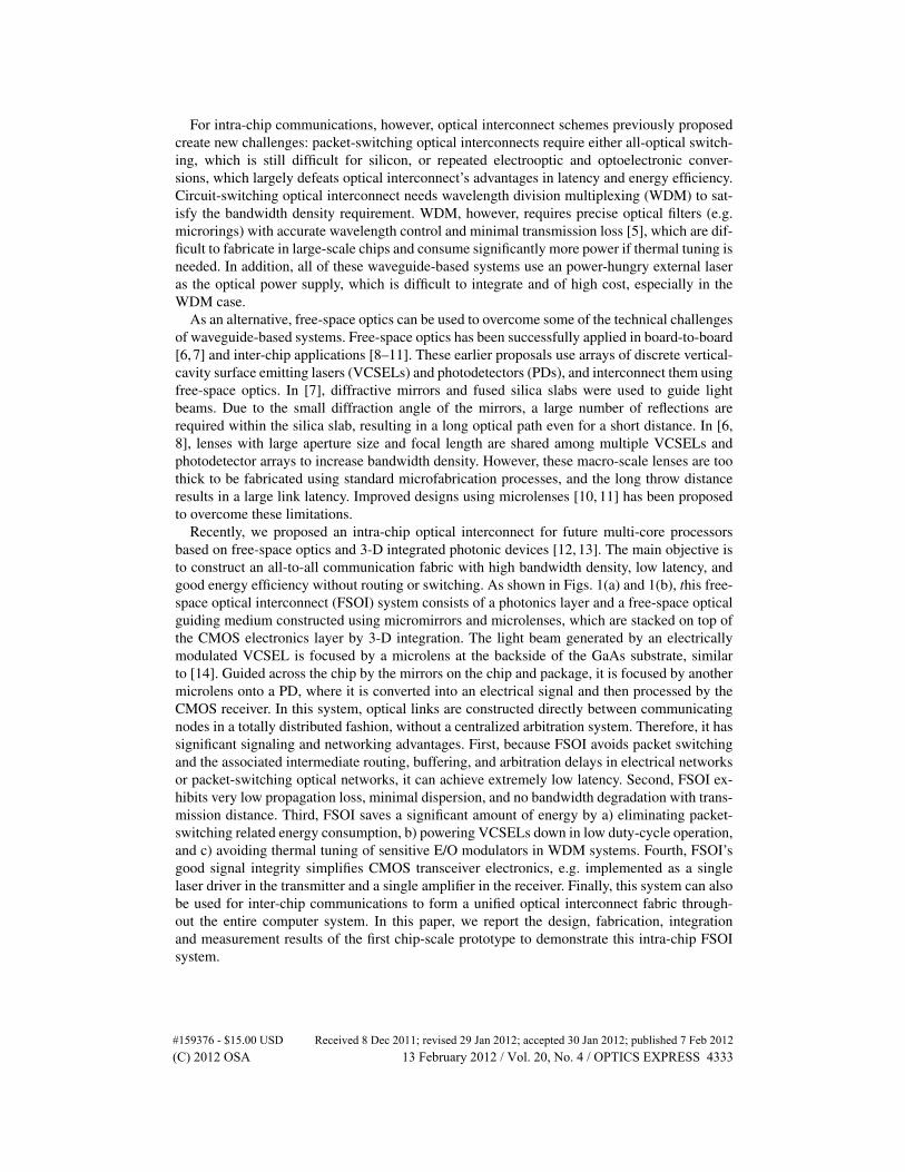
Recently, we proposed an intra-chip optical interconnect for future multi-core processorsbased on free-space optics and 3-D integrated photonic devices [12, 13]. The main objective isto construct an all-to-all communication fabric with high bandwidth density, low latency, andgood energy efficiency without routing or switching. As shown in Figs. 1(a) and 1(b), this free-space optical interconnect (FSOI) system consists of a photonics layer and a free-space opticalguiding medium constructed using micromirrors and microlenses, which are stacked on top ofthe CMOS electronics layer by 3-D integration. The light beam generated by an electricallymodulated VCSEL is focused by a microlens at the backside of the GaAs substrate, similarto [14]. Guided across the chip by the mirrors on the chip and package, it is focused by anothermicrolens onto a PD, where it is converted into an electrical signal and then processed by theCMOS receiver. In this system, optical links are constructed directly between communicatingnodes in a totally distributed fashion, without a centralized arbitration system. Therefore, it hassignificant signaling and networking advantages. First, because FSOI avoids packet switchingand the associated intermediate routing, buffering, and arbitration delays in electrical networksor packet-switching optical networks, it can achieve extremely low latency. Second, FSOI ex-hibits very low propagation loss, minimal dispersion, and no bandwidth degradation with trans-mission distance. Third, FSOI saves a significant amount of energy by a) eliminating packet-switching related energy consumption, b) powering VCSELs down in low duty-cycle operation,and c) avoiding thermal tuning of sensitive E/O modulators in WDM systems. Fourth, FSOI’sgood signal integrity simplifies CMOS transceiver electronics, e.g. implemented as a singlelaser driver in the transmitter and a single amplifier in the receiver. Finally, this system can alsobe used for inter-chip communications to form a unified optical interconnect fabric through-out the entire computer system. In this paper, we report the design, fabrication, integrationand measurement results of the first chip-scale prototype to demonstrate this intra-chip FSOIsystem.
#159376 - $15.00 USD Received 8 Dec 2011; revised 29 Jan 2012; accepted 30 Jan 2012; published 7 Feb 2012(C) 2012 OSA 13 February 2012 / Vol. 20, No. 4 / OPTICS EXPRESS 4333
Hyb
rid
Photo
nics
CM
OS
Elect
ronic
s
Free-
Spa
ce
Opt
ics
PD
Chip Package
Inter-chip
link
Micromirror
Microlens
/Microprism
Solder
bumps
Through
Silicon Via
Flip-chip
bond
Dielectric
Metal
GaAs
Silicon
VCSEL
Ge
(a)
GaAs
substrate
MicrolensMicromirror
Solder Bumps
Silicon Substrate
Ge PDs
Dielectric
layer
Chip-Package
(b)
Fig. 1. (a) Cross-sectional and (b) 3-D view of the proposed FSOI system implemented asa 3-D integrated chip stack for a multi-core microprocessor. Note that the VCSEL arraysare in the center and the photodetectors are on the periphery within each core.
2. Performance evaluation
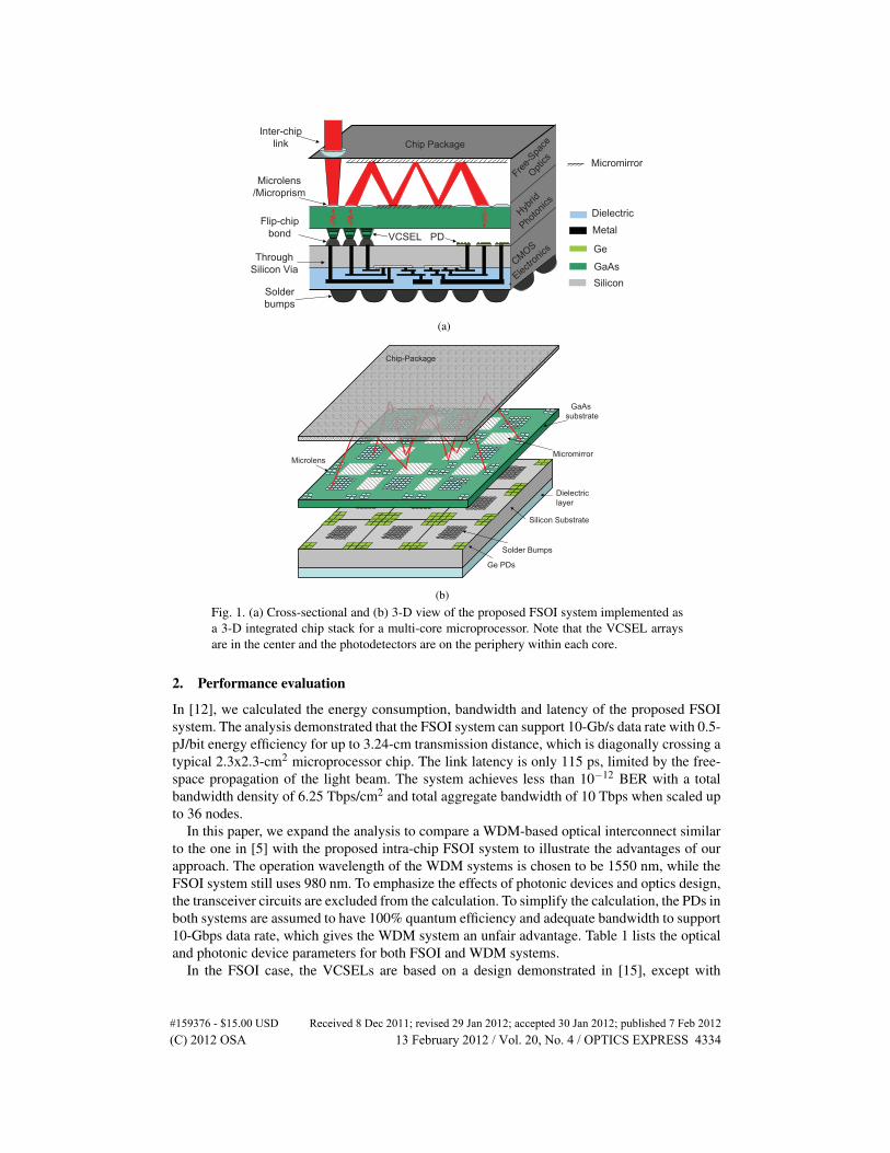
In [12], we calculated the energy consumption, bandwidth and latency of the proposed FSOIsystem. The analysis demonstrated that the FSOI system can support 10-Gb/s data rate with 0.5-pJ/bit energy efficiency for up to 3.24-cm transmission distance, which is diagonally crossing atypical 2.3x2.3-cm2 microprocessor chip. The link latency is only 115 ps, limited by the free-space propagation of the light beam. The system achieves less than 10−12 BER with a totalbandwidth density of 6.25 Tbps/cm2 and total aggregate bandwidth of 10 Tbps when scaled upto 36 nodes.
In this paper, we expand the analysis to compare a WDM-based optical interconnect similarto the one in [5] with the proposed intra-chip FSOI system to illustrate the advantages of ourapproach. The operation wavelength of the WDM systems is chosen to be 1550 nm, while theFSOI system still uses 980 nm. To emphasize the effects of photonic devices and optics design,the transceiver circuits are excluded from the calculation. To simplify the calculation, the PDs inboth systems are assumed to have 100% quantum efficiency and adequate bandwidth to support10-Gbps data rate, which gives the WDM system an unfair advantage. Table 1 lists the opticaland photonic device parameters for both FSOI and WDM systems.
In the FSOI case, the VCSELs are based on a design demonstrated in [15], except with
#159376 - $15.00 USD Received 8 Dec 2011; revised 29 Jan 2012; accepted 30 Jan 2012; published 7 Feb 2012(C) 2012 OSA 13 February 2012 / Vol. 20, No. 4 / OPTICS EXPRESS 4334
Table 1. Photonic Device Parameters for the FSOI and WDM Optical Interconnect SystemsVCSEL Microring Modulator
λ0 980 nm λ0 1550 nmf3dB 13 GHz f3dB 9.6 GHz
ηSlope 0.67 W/A FSR 10 nmηWall plug 30% Q 20000
Ith 0.14 mA δλ 0.07 nmIon 0.47 mA ∆λ 0.383 nmV f 1.62 V ILmod 0.0437 dB
Energy 0.069 fJ/bit Vr 7.5 VC j 6.6 fF
Energy 183 fJ/bit
PD in FSOI PD in WDM
ηquantum 100% ηquantum 100%RPD 0.79 A/W RPD 1.247 A/W
Lens/Mirror Waveguide
ILlens 0.1 dB αWG 0.3 dB/cmILmirror 0.08 dB ILbend 0.05 dB
δλ : laser linewidth ∆λ : off-tune wavelength shift
In0.2Ga0.8As quantum wells and GaAs barriers. The optical transmission loss is calculated byadding an insertion loss of 0.1-dB for a microlens and 0.08-dB for a mirror. Gaussian beamclipping loss at the lenses is determined by beam divergence and lens aperture size. As thenumber of nodes increases, the size of the lenses are shrunk to satisfy that up to 50% of chiparea is covered by microlenses, and hence optical clipping loss at the lenses increase from 0 at4 nodes up to 47% at 64 nodes.
In the WDM system, the light source is an external WDM laser, which is assumed to have20% efficiency, several times larger than the state-of-the-arts. The silicon microring modulatorsare based on the design in [16], operating in the carrier depletion mode. The microrings have10-µm radius with zero power transmission at the through port when the resonance is tunedto 1550 nm. As a good compromise between microring insertion loss and modulation powerconsumption, ∆λ is chosen to be 0.383 nm, leading to a 0.0437-dB insertion loss (ILmod) whenthe microring is off-tuned to make the waveguide transparent to optical data flux. A 0.77-nmwavelength channel spacing and a total of 13 channels in each node are selected to utilize theentire 10-nm free-spectral-range (FSR). Each channel experiences an additional 0.0662-dB lossper node (ILmod2) due to the contribution from microrings for the other 12 adjacent channels.Hence, the total modulator induced optical insertion loss per node increases to 0.11 dB. Theoverall link optical loss is calculated by adding 0.3-dB/cm waveguide loss [17], which is veryoptimistic, 0.05-dB bend loss, and 0.11-dB modulator insertion loss per node.
The chip has N communication nodes equally spaced in a√
N ×√
N grid. The chip size is2.3×2.3 cm2, typical for microprocessors [18]. The longest path is calculated by multiplyingthe distance between two adjacent nodes, L/
√N, where L=2.3 cm is the chip dimension, with
the number of nodes traveled, N − 1. In addition, there are also 2× (√
N − 1) bends on thewaveguide. Adding these two loss terms, the waveguide related optical loss for the longest pathcan be expressed as:
ILWG =L√N× (N −1)×αWG +2× (
√N −1)× ILbend (1)
where αWG=0.3 dB/cm is the waveguide loss and ILbend=0.05 dB is the waveguide bendingloss. The total modulator induced optical loss for the longest path is:
ILmodulators = N × (ILmod + ILmod2) (2)
#159376 - $15.00 USD Received 8 Dec 2011; revised 29 Jan 2012; accepted 30 Jan 2012; published 7 Feb 2012(C) 2012 OSA 13 February 2012 / Vol. 20, No. 4 / OPTICS EXPRESS 4335

0 20 40 600
5
10
15
Number of Nodes (N)
Optical Loss (
dB
)
FSOI
WG+Mod
WG
Mod
(a)
0 20 40 600
0.5
1
1.5
Number of Nodes (N)
Energ
y/b
it (
pJ/b
it)
FSOI
WDM
Modulator
(b)
Fig. 2. The calculated (a) optical loss and (b) energy efficiency of the FSOI and WDM-based optical interconnect systems with respect to increasing number of nodes. The break-down of the loss components for the WDM system is shown with dash lines. In this cal-culation, the transceiver electronics (laser driver and receiver) are not included in the totalpower consumption.
where ILmod=0.0438 dB and ILmod2=0.0662 dB. The total optical transmission loss for thelongest path is hence:
ILWDM =2.3√
N× (N −1)×0.3+2× (
√N −1)×0.05+N × (0.0438+0.0662) dB
= 0.69N −1√
N+0.1(
√N −1)+0.11N dB (3)
The optical transmission loss for the longest path in both systems are plotted in Fig. 2(a). Theoptical loss in the WDM system increases much faster than FSOI with the number of nodes.This can be mainly attributed to the linear increase of the modulator insertion loss with N.
Next we compare the energy efficiency of a single link in both systems. Assuming that therequired output current from the PDs in both systems is 150 µA, the laser/modulator opticalpower is calculated based on the optical loss, followed by their energy consumption. For exam-ple, the VCSEL and external WDM laser (per wavelength) need to provide 0.32 and 0.84-mWmaximum optical power at 36 nodes, respectively. The average electrical power consumed fora single WDM link is 6.1 mW, corresponding to 0.61-pJ/bit at 10-Gbps data rate, including0.183 pJ/bit to switch on/off the modulator. A VCSEL in the FSOI system consumes 0.69-mWaverage power, corresponding to a 0.069-pJ/bit energy efficiency. The energy efficiencies ofboth systems are shown in Fig. 2(b). The FSOI system performs better with N scaling, thanksto its lower optical loss.
Note that the calculations are highly optimistic for the WDM system. First, it does not includethe power consumption for thermal tuning, required to accurately control the wavelengths ofmicrorings. Second, the state-of-the-art WDM laser sources have energy efficiency of a fewpercentage, much worse than our assumption. Finally and more importantly, silicon microringmodulators exhibits insertion loss more than 0.5 dB [16, 19], resulting in over 60-dB opticalloss in a single 36-node link.
3. Design of FSOI chip prototype
As shown in Fig. 3, the chip-scale prototype of the proposed intra-chip FSOI system is con-structed as a 3-D chip stack. It is designed based on the following specifications and constraints:
#159376 - $15.00 USD Received 8 Dec 2011; revised 29 Jan 2012; accepted 30 Jan 2012; published 7 Feb 2012(C) 2012 OSA 13 February 2012 / Vol. 20, No. 4 / OPTICS EXPRESS 4336

Ge Substrate
Fused Silica
Glass Prism
MSM Ge PD
PadTransmission
line
200 µm 220 µm
525 µm
380 µm
0.75 cm
Gold
Silica
VCSEL Chip
GaAs
Si3N4
Spacer Spacer
Fig. 3. Cross-sectional view of the chip-level intra-chip FSOI prototype.
the chip has an area of 1×1 cm2, limited by the mask writer, mask size and autostepper lithog-raphy tools. The longest optical path is 1.4 cm, diagonally crossing the chip. The Ge substrateis used to build PDs and serve as a carrier for the VCSELs and microlenses. The microlensesare fabricated on a 525-µm thick fused silica substrate. The VCSELs used in the prototype isa commercial VCSEL array (Finisar V850-2092-001S, 1x4 array) with a pitch size of 250 µm,and provides 2-mW optical power at 850-nm with a 5-GHz modulation bandwidth. The pitchsize between microlenses is chosen as 250-µm, matching the pitch size of the VCSEL array.To facilitate wirebonding VCSELs and PDs to the Ge carrier, a silica spacer is inserted be-tween the microlenses and the VCSEL/PDs. A prism is used instead of micromirrors for testingconvenience.
3.1. Optics design
The optics design involves several device parameters: VCSEL aperture size/divergence angle,microlens aperture size and focal length, and device spacing, as shown in Fig. 4. The 850-nmVCSEL has an aperture size of 8 µm, and the full-width half-maximum (FWHM) far-fielddivergence angle is measured as 20o in free space at the operation bias point. Since there is a200-µm height difference between the VCSEL chip and PD, the microlens aperture and focallength need to be adjusted correspondingly. The VCSELs and PDs are located 200-µm and400-µm away from the back of the fused silica layer, or 565-µm and 765-µm from the lensesin air. The corresponding focal lengths are slightly less than these values because VCSELs andPDs need to be placed further away from the focal planes.
As discussed later in Sec. 4, microlenses are fabricated based on the photoresist melt-and-reflow technique. The desired microlens aperture size is defined by lithography, and its focallength is achieved by choosing the specific photoresist thickness. Assuming that the VCSELis placed near the focal point of the VCSEL lens to capture more than 98% of the light, theminimal aperture size should be 200 µm. The corresponding photoresist thickness to achievea 200-µm aperture and a 560-µm focal length lens is 10 µm. Similarly, the same photoresistthickness results in 725-µm focal length for a 220-µm aperture microlens on the PD side.
Using the designed focal length and aperture sizes, the beam waist size and its distance fromthe VCSEL microlens is calculated with respect to ∆z, the relative position of the VCSEL to thefocal point of its microlens, based on Gaussian beam propagation. As shown in Fig. 5, the beamwaist distance after the VCSEL lens is larger than 7 mm, i.e., half of the longest link distance,
#159376 - $15.00 USD Received 8 Dec 2011; revised 29 Jan 2012; accepted 30 Jan 2012; published 7 Feb 2012(C) 2012 OSA 13 February 2012 / Vol. 20, No. 4 / OPTICS EXPRESS 4337

Fused Silica
Dlens,PD=220 µm
200 µm
VCSELPD
200 µm
525 µm
Wo = 8 µm
=20o
Dlens,VCSEL=200 µm
Germanium substrate
Beam Waist
Fig. 4. Schematic of the FSOI link designed for the chip prototype. The total distance is1.4 cm, corresponding to crossing the chip diagonally.
0 10 20 30 4060
80
100
120
140
160
180
Beam
Wais
t S
ize (
µm
)
∆z =z−f
3
4
5
6
7
8
Beam
Wais
t D
ista
nce (
mm
)
Requiredbeam waist for L=1.4 cm
Fig. 5. Calculated beam waist size and position from the VCSEL microlens. The beamwaist distance needs to be 7 mm or longer for a 1.4-cm throw distance.
when the VCSEL is placed between 10 µm and 40 µm away from the lens. Within this range,the beam waist size changes between 110 µm and 160 µm. Cascading it with the PD lens, thenormalized optical power transmitted through the lenses for the 1.4-cm link distance is plottedwith respect to ∆z in Fig. 6(a), when the PD is assumed to capture all incoming light. Opticaltransmission peaks at ∆z between 10 and 20 µm, matching that of the beam waist distance inFig. 5.
Considering the power loss due to the finite PD size, the detected optical power is calculatedas shown in Fig. 6(b). The detected power does not change for PDs beyond 45-µm PD diameter.Adding tolerance for possible integration errors, the PD size is chosen as 62×62 µm2. Next,we evaluate the optical loss with respect to its distance for different ∆z. As shown in Fig. 7(a),smaller ∆z leads to better transmission at longer distances primarily because of the smallerdivergence angle. When ∆z=8 µm, the total transmission loss from the VCSEL to the PD isapproximately 2 dB for link distance up to 1.4 cm, and increases to 9.3 dB at 3.5 cm.
The impact of misalignment of the VCSEL and PD with their microlenses is also examined.As shown in Fig. 7(b), when the VCSEL is misaligned to the central axis of its microlens, theoptical transmission does not change for in-plane misalignments up to 6 µm at 1-cm distance.At 1.4-cm and 2-cm distance, the transmission decreases by 3 dB for a misalignment of 4.5 µmand 2.5 µm, respectively. To keep the transmission loss below 1 dB at 1.4 cm, the misalignmentneeds to be less than 3 µm, which is within the accuracy of typical flip-chip bonding processes.
#159376 - $15.00 USD Received 8 Dec 2011; revised 29 Jan 2012; accepted 30 Jan 2012; published 7 Feb 2012(C) 2012 OSA 13 February 2012 / Vol. 20, No. 4 / OPTICS EXPRESS 4338

0 10 20 30 40 50−5
−4
−3
−2
−1
0
∆z=z−f (µm)
Optical T
ransm
issio
n (
dB
)
lens1
lens2
total
(a)
0 10 20 30 40 50−8
−7
−6
−5
−4
−3
−2
−1
∆z=z−f (µm)
Optical T
ransm
issio
n (
dB
)
Dlens,PD
= 20 µm
Dlens,PD
= 30 µm
Dlens,PD
= 45 µm
Dlens,PD
= 60 µm
(b)
Fig. 6. Calculated optical transmission (a) when the PD capture all incoming light and (b)for different PD size, with respect to relative position of the VCSEL to the focal point of itsmicrolens. The link distance is 1.4 cm, and the light bounces twice on the 95% reflectivemirrors. Note that all incoming light is captured by the PD larger than 45-µm.
1 1.5 2 2.5 3 3.5
−12
−10
−8
−6
−4
−2
0
Distance (cm)
Optical T
ransm
issio
n (
dB
)
∆z=8µm
∆z=20µm
∆z=32µm
(a)
0 1 2 3 4 5 6−20
−15
−10
−5
0
+/− ∆R (µm)
Optical T
ransm
issio
n (
dB
)
L = 1cm
L = 1.4cm
L = 2cm
(b)
Fig. 7. Calculated optical transmission (a) with respect to optical pathway at different rela-tive distances of the VCSEL to microlens focal point and (b) for in-plane misalignment ofthe VCSEL source with respect to central axis of the lens at different distances.
3.2. Signaling
In order to evaluate the whole link performance, the values of the PD responsivity, VCSEL slopeefficiency, and the device bandwidth are needed. Based on our prior work [20], an MSM Ge PDwith a hydrogenated amorphous Si (a-Si:H) layer is designed and simulated in DAVINCI. Thea-Si layer increases the Schottky barrier height of holes, and passivates the Ge surface states. Ithence mitigates the large dark current and low frequency gain of the MSM PD. A 62×62-µm2
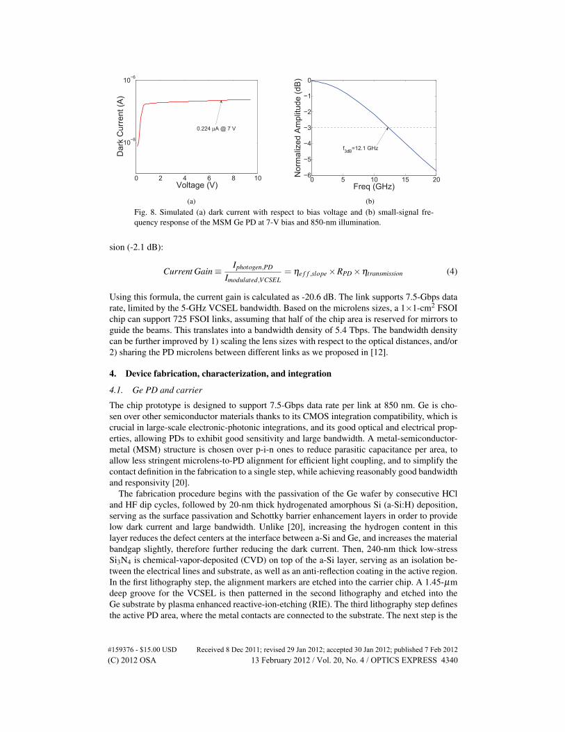
device with a 20-nm thick a-Si:H layer, 1.25-µm contact width, 2-µm contact spacing, anda low stress 106-nm thick Si3N4 anti-reflection coating achieves 0.37-A/W responsivity and0.224-µA dark current at 7-V bias (Fig. 8(a)). As shown in Fig. 8(b), the simulated bandwidthis 12.1 GHz with a 80 fF device capacitance, corresponding to a 40-GHz extrinsic bandwidthwhen terminated with 50 Ω. The commercial VCSEL has a slope efficiency of 0.4 W/A and2-mW optical power at 850-nm.
In a single-bit FSOI link, the electrical-to-electrical link gain is expressed as the product ofthe VCSEL slope efficiency (0.4 W/A), PD responsivity (0.37 A/W) and the optical transmis-
#159376 - $15.00 USD Received 8 Dec 2011; revised 29 Jan 2012; accepted 30 Jan 2012; published 7 Feb 2012(C) 2012 OSA 13 February 2012 / Vol. 20, No. 4 / OPTICS EXPRESS 4339
0 2 4 6 8 10
10−8
10−6
Voltage (V)
Dark
Curr
ent (A
)0.224 µA @ 7 V
(a)
0 5 10 15 20−6
−5
−4
−3
−2
−1
0
Freq (GHz)
Norm
aliz
ed A
mplit
ude (
dB
)
f3dB
=12.1 GHz
(b)
Fig. 8. Simulated (a) dark current with respect to bias voltage and (b) small-signal fre-quency response of the MSM Ge PD at 7-V bias and 850-nm illumination.
sion (-2.1 dB):
Current Gain ≡Iphotogen,PD
Imodulated,VCSEL= ηe f f ,slope ×RPD ×ηtransmission (4)
Using this formula, the current gain is calculated as -20.6 dB. The link supports 7.5-Gbps datarate, limited by the 5-GHz VCSEL bandwidth. Based on the microlens sizes, a 1×1-cm2 FSOIchip can support 725 FSOI links, assuming that half of the chip area is reserved for mirrors toguide the beams. This translates into a bandwidth density of 5.4 Tbps. The bandwidth densitycan be further improved by 1) scaling the lens sizes with respect to the optical distances, and/or2) sharing the PD microlens between different links as we proposed in [12].
4. Device fabrication, characterization, and integration
4.1. Ge PD and carrier
The chip prototype is designed to support 7.5-Gbps data rate per link at 850 nm. Ge is cho-sen over other semiconductor materials thanks to its CMOS integration compatibility, which iscrucial in large-scale electronic-photonic integrations, and its good optical and electrical prop-erties, allowing PDs to exhibit good sensitivity and large bandwidth. A metal-semiconductor-metal (MSM) structure is chosen over p-i-n ones to reduce parasitic capacitance per area, toallow less stringent microlens-to-PD alignment for efficient light coupling, and to simplify thecontact definition in the fabrication to a single step, while achieving reasonably good bandwidthand responsivity [20].
The fabrication procedure begins with the passivation of the Ge wafer by consecutive HCland HF dip cycles, followed by 20-nm thick hydrogenated amorphous Si (a-Si:H) deposition,serving as the surface passivation and Schottky barrier enhancement layers in order to providelow dark current and large bandwidth. Unlike [20], increasing the hydrogen content in thislayer reduces the defect centers at the interface between a-Si and Ge, and increases the materialbandgap slightly, therefore further reducing the dark current. Then, 240-nm thick low-stressSi3N4 is chemical-vapor-deposited (CVD) on top of the a-Si layer, serving as an isolation be-tween the electrical lines and substrate, as well as an anti-reflection coating in the active region.In the first lithography step, the alignment markers are etched into the carrier chip. A 1.45-µmdeep groove for the VCSEL is then patterned in the second lithography and etched into theGe substrate by plasma enhanced reactive-ion-etching (RIE). The third lithography step definesthe active PD area, where the metal contacts are connected to the substrate. The next step is the
#159376 - $15.00 USD Received 8 Dec 2011; revised 29 Jan 2012; accepted 30 Jan 2012; published 7 Feb 2012(C) 2012 OSA 13 February 2012 / Vol. 20, No. 4 / OPTICS EXPRESS 4340
Ti/Au Contacts
Germanium Substrate
Undoped Amorphous Silicon 22 nm
98 nm
Si3N4Si3N4
Si3N4
(a)
0 2 4 6 80
0.1
0.2
0.3
0.4
0.5
DC Bias (V)
Re
sp
on
siv
ity (
A/W
)
0
2
4
6
8
Da
rk C
urr
en
t (µ
A)
(b)
0
0.2
0.4
0.6
0.8
1
Time (0.1ns/div)
No
rma
lize
d A
mp
litu
de
(a
.u)
10 V
7 V
τFWHM
= 47 ps @ 7 V
τFWHM
= 45 ps @ 10 V
τf = 32.2 ps @ 7 V
τf = 31.8 ps @ 10 V
τr = 31.5 ps
(c)
0 5 10 15−20
−15
−10
−5
0
5
Freq (GHz)N
orm
aliz
ed
Am
plit
ud
e (
dB
)
10 V
7 V
f3dB
= 9.45 GHz
f3dB
= 10.05 GHz
(d)
Fig. 9. The fabricated 62×62-µm2 Ge MSM PD with 98-nm Si3N4 anti-reflection coatingunder 850-nm illumination: (a) PD structure, (b) responsivity and dark current, (c) impulseresponse using 50-GHz sampling oscilloscope at 7-V and 10-V bias, (d) DFT convertedfrequency response. The dark current density is measured as 1.7 nA/µm2 at 7-V.
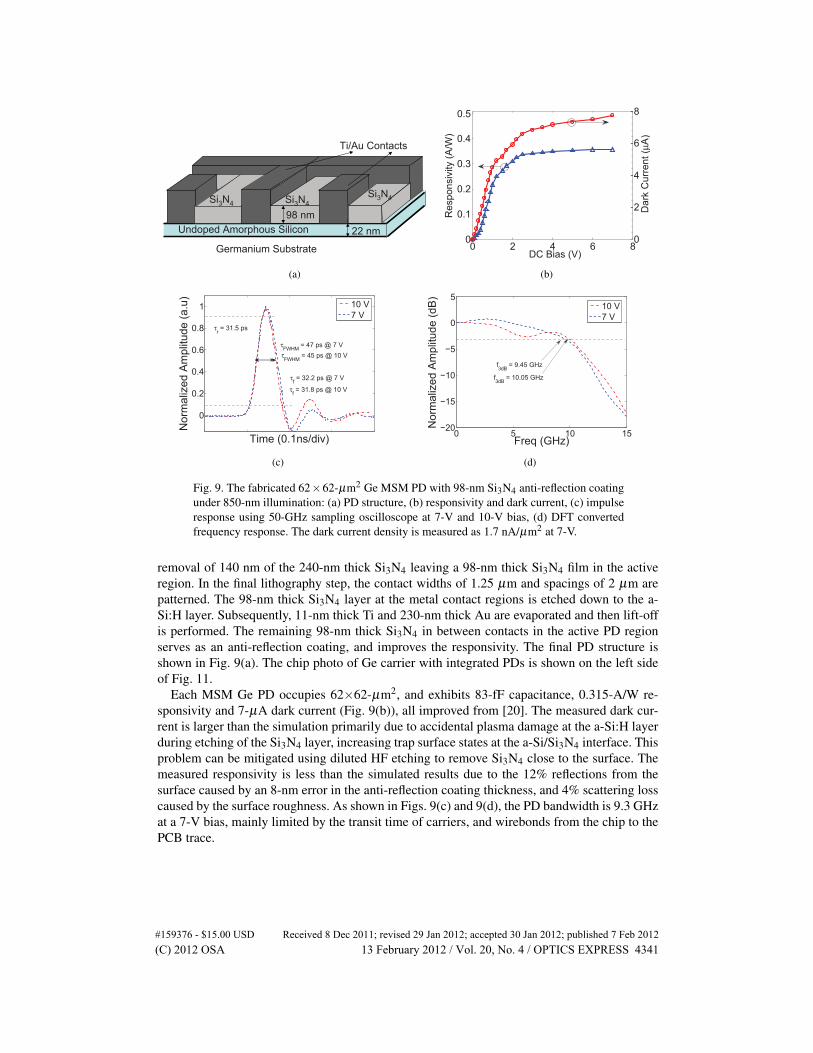
removal of 140 nm of the 240-nm thick Si3N4 leaving a 98-nm thick Si3N4 film in the activeregion. In the final lithography step, the contact widths of 1.25 µm and spacings of 2 µm arepatterned. The 98-nm thick Si3N4 layer at the metal contact regions is etched down to the a-Si:H layer. Subsequently, 11-nm thick Ti and 230-nm thick Au are evaporated and then lift-offis performed. The remaining 98-nm thick Si3N4 in between contacts in the active PD regionserves as an anti-reflection coating, and improves the responsivity. The final PD structure isshown in Fig. 9(a). The chip photo of Ge carrier with integrated PDs is shown on the left sideof Fig. 11.
Each MSM Ge PD occupies 62×62-µm2, and exhibits 83-fF capacitance, 0.315-A/W re-sponsivity and 7-µA dark current (Fig. 9(b)), all improved from [20]. The measured dark cur-rent is larger than the simulation primarily due to accidental plasma damage at the a-Si:H layerduring etching of the Si3N4 layer, increasing trap surface states at the a-Si/Si3N4 interface. Thisproblem can be mitigated using diluted HF etching to remove Si3N4 close to the surface. Themeasured responsivity is less than the simulated results due to the 12% reflections from thesurface caused by an 8-nm error in the anti-reflection coating thickness, and 4% scattering losscaused by the surface roughness. As shown in Figs. 9(c) and 9(d), the PD bandwidth is 9.3 GHzat a 7-V bias, mainly limited by the transit time of carriers, and wirebonds from the chip to thePCB trace.
#159376 - $15.00 USD Received 8 Dec 2011; revised 29 Jan 2012; accepted 30 Jan 2012; published 7 Feb 2012(C) 2012 OSA 13 February 2012 / Vol. 20, No. 4 / OPTICS EXPRESS 4341
−100 −50 0 50 1000
5
10
15
20
Cu
rva
ture
He
igh
t (µ
m)
Distance (µm)
Lens Diameter=220 µm
X2+Y
2=(384)
2
Measured data
(a)
200 m Diameter Lens
Focused at back surface
220 m Diameter Lens
Focused at back surface
190 m
from surface
210 m
from surface
230 m
from surface
330 m
from surface
350 m
from surface
370 m
from surface
18 m
27 m
(b)
Fig. 10. (a) The measured shape of the photoresist after the melt and reflow process, (b)spot sizes of collimated beams at the back surface of the 200-µm and 220-µm aperturesize lenses. Based on the photoresist refractive index of 1.54 and the measured radius ofcurvature of 384 µm, the focal length in air is calculated as 710-µm for the 220-µm aper-ture lens. The peak-to-peak surface roughness is approximately 0.9 µm, corresponding toa measured 1-dB optical loss.
4.2. Microlenses
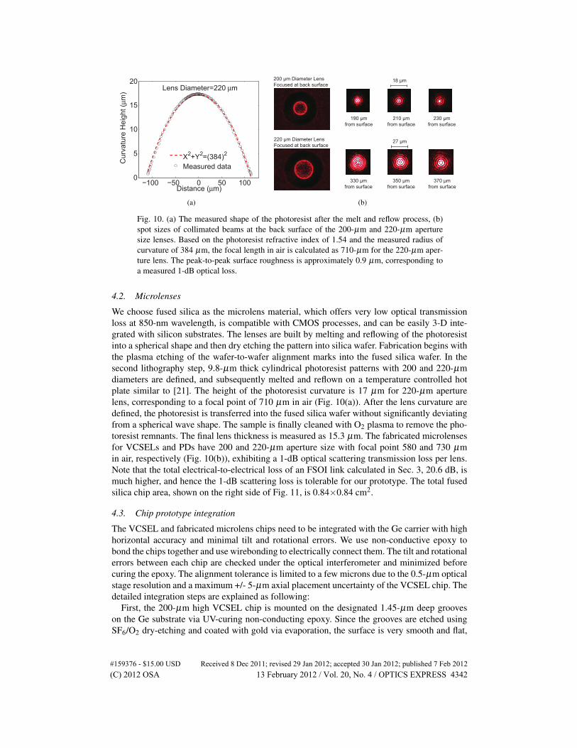
We choose fused silica as the microlens material, which offers very low optical transmissionloss at 850-nm wavelength, is compatible with CMOS processes, and can be easily 3-D inte-grated with silicon substrates. The lenses are built by melting and reflowing of the photoresistinto a spherical shape and then dry etching the pattern into silica wafer. Fabrication begins withthe plasma etching of the wafer-to-wafer alignment marks into the fused silica wafer. In thesecond lithography step, 9.8-µm thick cylindrical photoresist patterns with 200 and 220-µmdiameters are defined, and subsequently melted and reflown on a temperature controlled hotplate similar to [21]. The height of the photoresist curvature is 17 µm for 220-µm aperturelens, corresponding to a focal point of 710 µm in air (Fig. 10(a)). After the lens curvature aredefined, the photoresist is transferred into the fused silica wafer without significantly deviatingfrom a spherical wave shape. The sample is finally cleaned with O2 plasma to remove the pho-toresist remnants. The final lens thickness is measured as 15.3 µm. The fabricated microlensesfor VCSELs and PDs have 200 and 220-µm aperture size with focal point 580 and 730 µmin air, respectively (Fig. 10(b)), exhibiting a 1-dB optical scattering transmission loss per lens.Note that the total electrical-to-electrical loss of an FSOI link calculated in Sec. 3, 20.6 dB, ismuch higher, and hence the 1-dB scattering loss is tolerable for our prototype. The total fusedsilica chip area, shown on the right side of Fig. 11, is 0.84×0.84 cm2.
4.3. Chip prototype integration
The VCSEL and fabricated microlens chips need to be integrated with the Ge carrier with highhorizontal accuracy and minimal tilt and rotational errors. We use non-conductive epoxy tobond the chips together and use wirebonding to electrically connect them. The tilt and rotationalerrors between each chip are checked under the optical interferometer and minimized beforecuring the epoxy. The alignment tolerance is limited to a few microns due to the 0.5-µm opticalstage resolution and a maximum +/- 5-µm axial placement uncertainty of the VCSEL chip. Thedetailed integration steps are explained as following:
First, the 200-µm high VCSEL chip is mounted on the designated 1.45-µm deep grooveson the Ge substrate via UV-curing non-conducting epoxy. Since the grooves are etched usingSF6/O2 dry-etching and coated with gold via evaporation, the surface is very smooth and flat,
#159376 - $15.00 USD Received 8 Dec 2011; revised 29 Jan 2012; accepted 30 Jan 2012; published 7 Feb 2012(C) 2012 OSA 13 February 2012 / Vol. 20, No. 4 / OPTICS EXPRESS 4342
1- m contact spacing
0.75 cm
VCSEL chip areaPD array
250 m
220 m 200 m
62x62- m2
active area
2- m contact spacing1- m contact spacing
0.75 cm
VCSEL chip areaPD array
250 m
220 m 200 m
62x62- m2
active area
2- m contact spacing
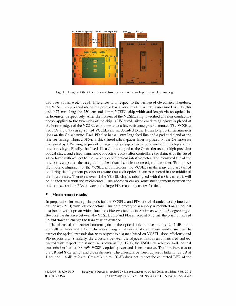
Fig. 11. Images of the Ge carrier and fused silica microlens layer in the chip prototype.
and does not have etch depth differences with respect to the surface of Ge carrier. Therefore,the VCSEL chip placed inside the groove has a very low tilt, which is measured as 0.15 µmand 0.27 µm along the 250-µm and 1-mm VCSEL chip width and length via an optical in-terferometer, respectively. After the flatness of the VCSEL chip is verified and non-conductiveepoxy applied to the two sides of the chip is UV-cured, silver conducting epoxy is placed atthe bottom edges of the VCSEL chip to provide a low resistance ground contact. The VCSELsand PDs are 0.75 cm apart, and VCSELs are wirebonded to the 1-mm long 50-Ω transmissionlines on the Ge substrate. Each PD also has a 1-mm long feed line and a pad at the end of theline for testing. Then, a 380-µm thick fused silica spacer layer is placed on the Ge substrateand glued by UV-curing to provide a large enough gap between bondwires on the chip and themicrolens layer. Finally, the fused silica chip is aligned to the Ge carrier using a high precisionoptical stage, and glued using non-conductive epoxy after controlling the flatness of the fusedsilica layer with respect to the Ge carrier via optical interferometer. The measured tilt of themicrolens chip after the integration is less than 4 µm from one edge to the other. To improvethe in-plane alignment of the VCSEL and microlens, the VCSELs in the array chip are turnedon during the alignment process to ensure that each optical beam is centered in the middle ofthe microlenses. Therefore, even if the VCSEL chip is misaligned with the Ge carrier, it willbe aligned well with the microlenses. This approach causes some misalignment between themicrolenses and the PDs; however, the large PD area compensates for that.
5. Measurement results
In preparation for testing, the pads for the VCSELs and PDs are wirebonded to a printed cir-cuit board (PCB) with RF connectors. This chip prototype assembly is mounted on an opticaltest bench with a prism which functions like two face-to-face mirrors with a 45 degree angle.Because the distance between the VCSEL chip and PDs is fixed at 0.75 cm, the prism is movedup and down to change the transmission distance.
The electrical-to-electrical current gain of the optical link is measured as -24.4 dB and -26.6 dB at 1-cm and 1.4-cm distances using a network analyzer. These results are used toextract the optical transmission with respect to distance based on VCSEL slope efficiency andPD responsivity. Similarly, the crosstalk between the adjacent links is also measured and ex-tracted with respect to distance. As shown in Fig. 12(a), the FSOI link achieves 4-dB opticaltransmission loss at 0.8-mW VCSEL optical power and 1-cm distance. The loss increases to5.3 dB and 8 dB at 1.4 and 2-cm distance. The crosstalk between adjacent links is -23 dB at1 cm and -16 dB at 2 cm. Crosstalk up to -20 dB does not impact the estimated BER of the
#159376 - $15.00 USD Received 8 Dec 2011; revised 29 Jan 2012; accepted 30 Jan 2012; published 7 Feb 2012(C) 2012 OSA 13 February 2012 / Vol. 20, No. 4 / OPTICS EXPRESS 4343
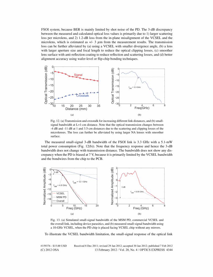
FSOI system, because BER is mainly limited by shot noise of the PD. The 3-dB discrepancybetween the measured and calculated optical loss values is primarily due to 1) larger scatteringloss per microlens, and 2) 1.2-dB loss from the in-plane misalignment of the VCSEL and themicrolens, which is estimated as +/- 3 µm from the measurement results. The transmissionloss can be further alleviated by (a) using a VCSEL with smaller divergence angle, (b) a lenswith larger aperture size and focal length to reduce the optical clipping losses, (c) smootherlens surface with anti-reflection coating to reduce reflection and scattering losses, and (d) betteralignment accuracy using wafer-level or flip-chip bonding techniques.
10 15 20 25 30 35−30
−25
−20
−15
−10
−5
0
Distance (mm)
Optical T
ransm
issio
n (
dB
)
Signal
Crosstalk
(a)
0 2 4 6 8−30
−25
−20
−15
−10
−5
0
Freq(GHz)
Optical T
ransm
issio
n (
dB
)
f3dB
= 3.3 GHz
(b)
Fig. 12. (a) Transmission and crosstalk for increasing different link distances, and (b) small-signal bandwidth at L=1-cm distance. Note that the optical transmission changes between-4 dB and -11 dB at 1 and 3.5-cm distances due to the scattering and clipping losses of themicrolenses. The loss can further be alleviated by using larger NA lenses with smoothersurface.
The measured small-signal 3-dB bandwidth of the FSOI link is 3.3 GHz with a 5.1-mWtotal power consumption (Fig. 12(b)). Note that the frequency response and hence the 3-dBbandwidth does not change with transmission distance. The bandwidth does not show any dis-crepancy when the PD is biased at 7 V, because it is primarily limited by the VCSEL bandwidthand the bondwires from the chip to the PCB.
0 5 10 15 20
−18
−15
−12
−9
−6
−3
0
Freq (GHz)
Norm
aliz
ed A
mplit
ude (
dB
)
VCSEL
MSM PD
Overall
f3dB
= 4.9 GHz
3 dB
f3dB
= 12.1 GHz
(a)
0 2 4 6 8−4
−3
−2
−1
0
1
2
Freq (GHz)
Norm
aliz
ed A
mplit
ude (
dB
)
3 dB
f3dB
= 6.55 GHz
(b)
Fig. 13. (a) Simulated small-signal bandwidth of the MSM PD, commercial VCSEL andthe overall link, including device parasitics, and (b) measured small-signal bandwidth usinga 10-GHz VCSEL, when the PD chip is placed facing VCSEL chip without any mirrors.
To illustrate the VCSEL bandwidth limitation, the small-signal response of the optical link
#159376 - $15.00 USD Received 8 Dec 2011; revised 29 Jan 2012; accepted 30 Jan 2012; published 7 Feb 2012(C) 2012 OSA 13 February 2012 / Vol. 20, No. 4 / OPTICS EXPRESS 4344
is simulated based on the experimental and simulation results of the photonics devices. Thesimulated bandwidth of the MSM PD is 12.1 GHz at 5-V bias, and the VCSEL has a modeledsmall-signal bandwidth of 5 GHz at 3 mA forward bias current and 1.7-V bias. The overallbandwidth is estimated as 4.9 GHz limited by the VCSEL bandwidth (Fig. 13(a)). To demon-strate the potential bandwidth of the FSOI link, a faster VCSEL from an earlier experiment andthe same PD are mounted on two PCBs and placed facing each other. The measured frequencyresponse of this setup is shown in Fig. 13(b). The -3-dB bandwidth is now 6.55 GHz, whichcan support a data rate of 9 Gbps.
6. Discussion
In order to further improve the chip prototype performance, the sensitivity of the PDs needsto be increased. Although MSM Ge PDs with the described barrier enhancement and surfacepassivation techniques reduce dark current by more than three orders of magnitude, these darkcurrent values are still high enough to affect the signal-to-noise ratio and bit-error-rate for theFSOI system adversely. For example, a PD with 7-µA dark current and the same optical powerlevels in the performance evaluation section, the bit error rate cannot be lower than 10−9 witha 0.5-pJ/bit energy efficiency at 10-Gb/s data rate. Simply burning more power at the VCSELto increase the signal-to-noise ratio reduces energy efficiency. Shrinking PD area, e.g., by morethan 10 times can reduce the dark current correspondingly, hence leading to a BER less than10−12. However, smaller PD area puts constraints on the microlens and optics design, requir-ing larger focal length and aperture size to achieve smaller spot size at the PD, and therefore,limiting the bandwidth density of the interconnect system. This can be overcome by designingone large lens to connect a link with multiple bits (VCSEL-PD pairs), similar to [8]. Alterna-tively, changing the PD device to a p-i-n structure can significantly reduce the dark current atthe expense of process complexity.
7. Conclusion
An intra-chip free-space optical interconnect (FSOI) system is presented. The FSOI systemachieves low loss, low latency, large bandwidth and large energy efficiency for future many-core chips. A performance evaluation shows that energy efficiency of the FSOI system is sig-nificantly better than the waveguide-based WDM optical interconnects for a large number ofnodes. The first 3-D integrated chip-scale prototype with a 1×1-cm2 area is designed based onreal-world optical and photonic device parameters. MSM PDs are fabricated on a Ge carrierchip, and GaAs VCSELs and fused silica microlenses are 3-D integrated on the Ge carrier. Theprototype achieves 4-dB optical loss, -23-dB crosstalk, and 3.3-GHz small signal bandwidth ata 1-cm transmission distance. The loss increases slightly to 5 dB with -21-dB crosstalk whenthe distance increases to 1.4 cm.
Acknowledgment
This work was partially supported by NSF grants CCF0829915 and DMR1124601, and theDOE Office of Inertial Confinement Fusion under Cooperative Agreement No. DE-FC52-08NA28302, the University of Rochester, and the New York State Energy Research and De-velopment Authority. The support of DOE does not constitute an endorsement by DOE of theviews expressed in this article. The authors would like to thank Cornell Nanofabrication Facilityfor their support.
#159376 - $15.00 USD Received 8 Dec 2011; revised 29 Jan 2012; accepted 30 Jan 2012; published 7 Feb 2012(C) 2012 OSA 13 February 2012 / Vol. 20, No. 4 / OPTICS EXPRESS 4345