Embed Size (px)
Citation preview

ELECTRONIC DEVICES AND CIRCUITS (EC301PC)
Poonam Swami, Asst.Professor Dept. Of ECE, KGRCET
3. Course Objectives Course Outcomes & Topic Outcome
COURSE OBJECTIVES
• To introduce components such as diodes, BJTs and FETs.
• To know the applications of components.
• To know the switching characteristics of components
• To give understanding of various types of amplifier circuits
COURSE OUTCOMES
At the end of the course, the student will be able to:
CO1: Interpret various applications of diode.
CO2: Classify various configurations and biasing technique of BJT.
CO3: Discuss operation, biasing and applications of JFET.
CO4: Demonstrate special purpose devices.
CO5: Distinguish various low frequency BJT amplifiers.
CO6: Design and analyze FET amplifier.

ELECTRONIC DEVICES AND CIRCUITS (EC301PC)
Poonam Swami, Asst.Professor Dept. Of ECE, KGRCET
Topic Outcome
Sr.
No
Topic to be covered At the end student will be able to
1 UNIT 1: DIODE AND APPLICATIONS
Semiconductor
Define semiconductor and its type.
2 Charge densities in p type and n type
semiconductor
Describe charge densities in p type
and n type semiconductor
3 Diode - Static and Dynamic resistances,
Equivalent circuit, Load line analysis
Relate Static and Dynamic
resistances, Equivalent circuit,
Discuss load line analysis
4 Diffusion and Transition Capacitances State diffusion and transition
capacitance
5 Diode Applications: Switch-Switching
times
State Switching times
6 Rectifier - Half Wave Rectifier Construct half wave rectifier
7 Full Wave Rectifier, Bridge Rectifier, Construct rectifiers
8 Tutorial - rectifiers Summarize rectifiers
9 Rectifiers with Capacitive and Inductive
Filters
Sketch Rectifiers with Capacitive
and Inductive Filters
10 Clippers-Clipping at two independent
levels
Show Clipping at two independent
levels
11 Clamper-Clamping Circuit Theorem Describe clamping circuit theorem
12 Clamping Operation, Types of Clampers. State types of clampers
13 UNIT 2: Bipolar Junction Transistor
Principle of Operation
Explain operation of BJT
14 Common Emitter Discuss common emitter
15 Common Base and Common Collector
Configurations
Discuss common base & common
collector configurations
16 Transistor as a switch Examine Transistor as a switch
17 switching times State switching times of transistor
18 Transistor Biasing and Stabilization -
Operating point, DC & AC load lines,
Summarize Operating point, DC &
AC load lines
19 Transistor Biasing and Stabilization -
Operating point, DC & AC load lines,
Summarize Operating point, DC &
AC load lines
20 Biasing - Fixed Bias Illustrate fixed bias
21 Self Bias Illustrate self bias
22 Bias Stability Illustrate stability
23 Problems and revision on biasing methods. Solve different biasing methods

ELECTRONIC DEVICES AND CIRCUITS (EC301PC)
Poonam Swami, Asst.Professor Dept. Of ECE, KGRCET
24 Bias Compensation using Diodes. Define bias compensation
25 Tutorial – transistor biasing Summarize transistor biasing
26 UNIT3: Junction Field Effect Transistor
(FET) Construction
Construct JFET
27 Principle of Operation Discuss operation of FET
28 Pinch-Off Voltage & Volt- Ampere
Characteristic
Define pinch off voltage & sketch
V-I characteristics
29 Comparison of BJT and FET Compare BJT & FET
30 Biasing of FET List biasing of FET
31 Biasing of FET Summarize basing of FET
32 FET as Voltage Variable Resistor Experiment voltage variable resistor
33 Tutorial-biasing of FET Summarize biasing of FET
34 Special Purpose Devices: Zener Diode –
Characteristics
Label Zener Characteristics
35 Voltage Regulator Show voltage regulator
36 Principle of Operation - SCR, Discuss SCR
37 Principle of Operation - Tunnel diode Discuss tunnel diode
38 Principle of Operation - UJT Discuss UJT
39 Principle of Operation- Varactor Diode. Discuss varactor diode
40 Tutorial- special purpose diodes Summarize special purpose diodes
41 UNIT IV- Analysis and Design of Small
Signal Low Frequency BJT Amplifiers
Transistor Hybrid model
Sketch Transistor Hybrid model
42 Determination of h-parameters from
transistor characteristics
Prepare h-parameters from transistor
characteristics
43 Typical values of h- parameters in CE, CB
and CC configurations
List Typical values of h- parameters
in CE, CB and CC configurations
44 Transistor amplifying action Define Transistor amplifying action
45 Analysis of CE Analyze CE
46 Analysis of CE Analyze CE
47 Analysis of CC,CB Amplifier Analyze CC,CB
48 Tutorial - Analysis of CE Summarize analysis of CE
49 Examples on analysis Solve small signal analysis for BJT
50 CE Amplifier with emitter resistance Relate CE Amplifier with emitter

ELECTRONIC DEVICES AND CIRCUITS (EC301PC)
Poonam Swami, Asst.Professor Dept. Of ECE, KGRCET
resistance
51 low frequency response of BJT Amplifiers Illustrate low frequency response of
BJT Amplifiers
52 low frequency response of BJT Amplifiers Illustrate low frequency response of
BJT Amplifiers
53 Effect of coupling and bypass capacitors on
CE Amplifier.
State Effect of coupling and bypass
capacitors on CE Amplifier
54 Tutorial- low frequency response of BJT
Amplifiers
Summarize low frequency response
of BJT Amplifiers
55 UNIT V: FET AMPLIFERS
Small Signal Model
Analyze small signal model
56 Analysis of JFET Amplifiers Analyze JFET amplifier
57 Analysis of JFET Amplifiers Analyze JFET amplifier
58 Analysis of CS JFET Amplifiers Construct CS JFET Amplifiers
59 Analysis of CD,CG JFET Amplifier Construct CD JFET Amplifiers
60 MOSFET Characteristics in Enhancement
& Depletion mode, Basic Concepts of
MOS Amplifiers.
Compare MOSFET Characteristics
in Enhancement & Depletion mode
Explain Basic Concepts of MOS
Amplifiers
61 Tutorial- Analysis of JFET Amplifiers Summarize analysis of JFET
amplifier.
62 Feedback amplifiers Define & list feedback amplifiers
63 Oscillators Discuss oscillators

ELECTRONIC DEVICES AND CIRCUITS (EC301PC)
Poonam Swami, Asst.Professor Dept. Of ECE, KGRCET
4. COURSE PRE–REQUISITES
a. Engineering Mathematics
b. Fundamentals of Engineering Physics
c. Basic Electronics

ELECTRONIC DEVICES AND CIRCUITS (EC301PC)
Poonam Swami, Asst.Professor Dept. Of ECE, KGRCET
5. Course Information Sheet
5. a). COURSE DESCRIPTION:
PROGRAMME: B. Tech. (Electronics and
Communication Engineering.)
DEGREE: BTECH
COURSE: ELECTRONIC DEVICES AND
CIRCUITS
YEAR: II SEM: I CREDITS: 4
COURSE CODE: EC301PC
REGULATION: R18
COURSE TYPE: COMPULSARY
COURSE AREA/DOMAIN: Design CONTACT HOURS: 3 (L)
hours/Week.
CORRESPONDING LAB COURSE
CODE (IF ANY):
YES
LAB COURSE NAME: EDC LAB
5. b). SYLLABUS:
Unit Details Hours
I
Diode and Applications: Diode - Static and Dynamic resistances,
Equivalent circuit, Load line analysis, Diffusion and Transition
Capacitances, Diode Applications: Switch-Switching times.
Rectifier - Half Wave Rectifier, Full Wave Rectifier, Bridge
Rectifier, Rectifiers with Capacitive and Inductive Filters, Clippers-
Clipping at two independent levels, Clamper-Clamping Circuit
Theorem, Clamping Operation, Types of Clampers.
9
II
Bipolar Junction Transistor (BJT): Principle of Operation,
Common Emitter, Common Base and Common Collector
Configurations, Transistor as a switch, switching times, Transistor
Biasing and Stabilization - Operating point, DC & AC load lines,
Biasing - Fixed Bias, Self Bias, Bias Stability, Bias Compensation
using Diodes.
12
III
Junction Field Effect Transistor (FET): Construction, Principle
of Operation, Pinch-Off Voltage, Volt- Ampere Characteristic,
Comparison of BJT and FET, Biasing of FET, FET as Voltage
Variable Resistor. Special Purpose Devices: Zener Diode -
Characteristics, Voltage Regulator. Principle of Operation - SCR,
Tunnel diode, UJT, Varactor Diode.
13
IV
Analysis and Design of Small Signal Low Frequency BJT
Amplifiers: Transistor Hybrid model, Determination of h-
parameters from transistor characteristics, Typical values of h-
12

ELECTRONIC DEVICES AND CIRCUITS (EC301PC)
Poonam Swami, Asst.Professor Dept. Of ECE, KGRCET
parameters in CE, CB and CC configurations, Transistor
amplifying action, Analysis of CE, CC, CB Amplifiers and CE
Amplifier with emitter resistance, low frequency response of BJT
Amplifiers, effect of coupling and bypass capacitors on CE
Amplifier.
V
FET Amplifiers: Small Signal Model, Analysis of JFET
Amplifiers, Analysis of CS, CD, CG JFET Amplifiers. MOSFET
Characteristics in Enhancement and Depletion mode, Basic
Concepts of MOS Amplifiers.
6
Contact classes for syllabus coverage 52
Lectures beyond syllabus 2
Classes for gaps &Add-on classes 2
Tutorial classes 7
Total No. of classes 63
5.c). GAPS IN THE SYLLABUS - TO MEET INDUSTRY/PROFESSION
REQUIREMENTS:
S.NO. DESCRIPTION PROPOSEDACTIONS No. of
lectures
1 Semiconductors Video 1
2 Charge densities in p type and
n type semiconductor
PPT 1
5.d). TOPICS BEYOND SYLLABUS/ADVANCED TOPICS:
S.NO. DESCRIPTION PROPOSEDACTIONS No. of
lectures
1 Feedback amplifier PPT 1
2 Oscillator Video 1

ELECTRONIC DEVICES AND CIRCUITS (EC301PC)
Poonam Swami, Asst.Professor Dept. Of ECE, KGRCET
5. e). WEB SOURCE REFERENCES:
S
r
.
N
o
.
Name of book/ website
a
.
http://www.nptelvideos.in/search?q=DIODE+AND+APPLICATIONS
b
.
http://www.nptelvideos.in/search?q=BJT+AMPLIFIER
c
.
http://www.nptelvideos.in/search?q=FET+AMPLIFIER
d
.
http://www.nptelvideos.in/search?q=SMALL+SIGNAL+ANALYSIS
5. f). DELIVERY/INSTRUCTIONAL METHODOLOGIES:
CHALK & TALK STUD.
ASSIGNMENT
WEB
RESOURCES
LCD/SMART BOARDS STUD.
SEMINARS
☐ ADD-ON
COURSES
5.g). ASSESSMENT METHODOLOGIES-DIRECT
ASSIGNMENTS
STUD.
SEMINARS
TESTS/MODEL
EXAMS
UNIV.
EXAMINATION
☐ STUD. LAB
PRACTICES
☐ STUD.
VIVA
☐
MINI/MAJOR
PROJECTS
☐
CERTIFICATIONS
☐ ADD-ON
COURSES
☐ OTHERS
5.h). ASSESSMENT METHODOLOGIES-INDIRECT
ASSESSMENT OF COURSE
OUTCOMES
(BY FEEDBACK, ONCE)
STUDENT FEEDBACK ON
FACULTY (TWICE)
☐ASSESSMENT OF MINI/MAJOR
PROJECTS BY EXT. EXPERTS
☐ OTHERS

ELECTRONIC DEVICES AND CIRCUITS (EC301PC)
Poonam Swami, Asst.Professor Dept. Of ECE, KGRCET
5.i). TEXT/REFERENCE BOOKS:
T/R BOOK TITLE/AUTHORS/PUBLICATION
Text Book Electronic Devices and Circuits- Jacob Millman, McGraw Hill
Education
Text Book Electronic Devices and Circuits theory– Robert L. Boylestead, Louis
Nashelsky, 11th Edition, 2009, Pearson.
Reference Book The Art of Electronics, Horowitz, 3rd Edition Cambridge University
Press
Reference Book Electronic Devices and Circuits, David A. Bell – 5th Edition,
Oxford.
Reference Book Pulse, Digital and Switching Waveforms –J. Millman, H. Taub and
Mothiki S. Prakash Rao, 2Ed., 2008, Mc Graw Hill.

ELECTRONIC DEVICES AND CIRCUITS (EC301PC)
Poonam Swami, Asst.Professor Dept. Of ECE, KGRCET
6. Micro Lesson Plan
Topic wise Coverage [Micro Lesson Plan]
Sr.
No.
Topic Scheduled
date
Actual
date
1 UNIT 1: DIODE AND APPLICATIONS
Semiconductor
2 Charge densities in p type and n type
semiconductor
3 Diode - Static and Dynamic resistances,
Equivalent circuit, Load line analysis
4 Diffusion and Transition Capacitances
5 Diode Applications: Switch-Switching
times
6 Rectifier - Half Wave Rectifier
7 Full Wave Rectifier, Bridge Rectifier,
8 Tutorial - rectifiers
9 Rectifiers with Capacitive and Inductive
Filters
10 Clippers-Clipping at two independent levels
11 Clamper-Clamping Circuit Theorem
12 Clamping Operation, Types of Clampers.
13 UNIT 2: Bipolar Junction Transistor
Principle of Operation
14 Common Emitter
15 Common Base and Common Collector
Configurations
16 Transistor as a switch
17 switching times
18 Transistor Biasing and Stabilization -
Operating point, DC & AC load lines,
19 Transistor Biasing and Stabilization -
Operating point, DC & AC load lines,

ELECTRONIC DEVICES AND CIRCUITS (EC301PC)
Poonam Swami, Asst.Professor Dept. Of ECE, KGRCET
20 Biasing - Fixed Bias
21 Self Bias
22 Bias Stability
23 Problems and revision on biasing methods.
24 Bias Compensation using Diodes.
25 Tutorial – transistor biasing
26 UNIT3: Junction Field Effect Transistor
(FET)
Construction
27 Principle of Operation
28 Pinch-Off Voltage & Volt- Ampere
Characteristic
29 Comparison of BJT and FET
30 Biasing of FET
31 Biasing of FET
32 FET as Voltage Variable Resistor
33 Tutorial-biasing of FET
34 Special Purpose Devices: Zener Diode –
Characteristics
35 Voltage Regulator
36 Principle of Operation - SCR,
37 Principle of Operation - Tunnel diode
38 Principle of Operation - UJT
39 Principle of Operation- Varactor Diode.
40 Tutorial- special purpose diodes
41 UNIT IV- Analysis and Design of Small
Signal Low Frequency BJT Amplifiers
Transistor Hybrid model
42 Determination of h-parameters from
transistor characteristics

ELECTRONIC DEVICES AND CIRCUITS (EC301PC)
Poonam Swami, Asst.Professor Dept. Of ECE, KGRCET
43 Typical values of h- parameters in CE, CB
and CC configurations
44 Transistor amplifying action
45 Analysis of CE
46 Analysis of CE
47 Analysis of CC,CB Amplifier
48 Tutorial - Analysis of CE
49 Examples on analysis
50 CE Amplifier with emitter resistance
51 low frequency response of BJT Amplifiers
52 low frequency response of BJT Amplifiers
53 Effect of coupling and bypass capacitors on
CE Amplifier.
54 Tutorial- low frequency response of BJT
Amplifiers
55 UNIT V: FET AMPLIFERS
Small Signal Model
56 Analysis of JFET Amplifiers
57 Analysis of JFET Amplifiers
58 Analysis of CS JFET Amplifiers
59 Analysis of CD,CG JFET Amplifier
60 MOSFET Characteristics in Enhancement
& Depletion mode, Basic Concepts of MOS
Amplifiers.
61 Tutorial- Analysis of JFET Amplifiers
62 Feedback amplifiers
63 Oscillators

ELECTRONIC DEVICES AND CIRCUITS (EC301PC)
Poonam Swami, Asst.Professor Dept. Of ECE, KGRCET
7. Teaching Schedule
Subject ELECTRONIC DEVICES AND CIRCUITS
Text Books (to be purchased by the Students)
Book 1 Millman's Electronic Devices and Circuits – J. Millman, C.C.Halkias,and Satyabrata
Jit, 2 Ed.,1998, TMH.
Book 2 Electronic Devices and Circuits – Mohammad Rashid, Cengage Learing, 2013
Reference Books
Book 3 Electronic Devices and Circuits – S.Salivahanan, N.Suresh Kumar, A.Vallavaraj, 2
Ed., 2008, TMH.
Book 4 Electronic Devices and Circuits – R.L. Boylestad and Louis Nashelsky,9 Ed., 2006,
PEI/PHI.
Unit
Topic
Chapters Nos No of
classes Book 1 Book 2 Book 3 Book 4
I
P-N Junction
Diode
1 1 1 1 9
Rectifiers and
Filters 8 7 11
II
Bipolar Junction
Transistor 9 6 6 12
III
Field Effect
Transistor 13 9
13 Special Purpose
Electronic
Devices
10 5 5
IV
Bipolar Junction
Transistor
amplifier
9 6 6 12
V
Field Effect
Transistor 13 9 6
Contact classes for syllabus coverage 52
Lectures beyond syllabus and gaps in syllabus 4
Tutorial classes 7
Total No. of classes 63

ELECTRONIC DEVICES AND CIRCUITS (EC301PC)
Poonam Swami, Asst.Professor Dept. Of ECE, KGRCET
11. MID exam Descriptive Question Papers

ELECTRONIC DEVICES AND CIRCUITS (EC301PC)
Poonam Swami, Asst.Professor Dept. Of ECE, KGRCET
SET NO: 1 II B.TECH I SEM (R18) ECE I MID EXAMINATIONS, SEPTEMBER-2019
SUBJECT NAME: ELECTRONIC DEVICES & CIRCUITS
OBJECTIVE EXAM
NAME_____________________________HALL TICKET NO
Answer all the questions. All questions carry equal marks. Time: 20min. 10 marks.
I choose correct alternative:
1. In a PN junction with no external voltage, the electric field between acceptor and
donor ions is called a
[ ]
A. Peak B. Barrier C. Threshold D. Path
2. For a P-N junction diode, the current in reverse bias may be [ ]
A. Few
miliamperes
B. Between 0.2 A and 15
A C. Few amperes
D. Few micro or nano
amperes
3. The maximum efficiency of a half-wave rectifier is ……………….. [ ]
A. 40.6 % B. 81.2 % C. 50 % D. 25 %
4. Which of the following is not a necessary component in a clamper circuit? [ ]
A) Diode B) Capacitor C) Resistor
D) Independent DC
Supply
5. Consider the following statements: A clamper circuit
1. Adds or subtracts a dc voltage to a waveform 2. does not change the waveform
3. Amplifies the waveform, Which are correct?
[ ]
A) 1, 2 B) 1, 3 C) 1, 2, 3 D) 2, 3
6. The base of a transistor is ………….. doped [ ]
A. heavily B. moderately C. lightly D. none of the above
7. In a transistor ……………….. [ ]
A. IC = IE + IB B. IB = IC + IE C. IE = IC – IB D. IE = IC + IB
8. In which region a transistor acts as an open switch? [ ]
A. cut off region B. inverted region C. active region D. saturated region
9. The relation between β and α is ………….. [ ]
A. β = 1 / (1 – α ) B. β = (1 – α ) / α C. β = α / (1 – α ) D. α / (1 + α )
10. Where should be the bias point set in order to make transistor work as an [ ]
A

ELECTRONIC DEVICES AND CIRCUITS (EC301PC)
Poonam Swami, Asst.Professor Dept. Of ECE, KGRCET
amplifier?
A) Cut off B) Active C) Saturation
D) Cut off and
Saturation
II Fill in the Blanks:
11. A circuit that removes positive or negative parts of waveform is called ___________.
12. A circuit that adds positive or negative dc voltage to an input sine wave is called
____________.
13. Transformer utilization factor of a centre tapped full wave rectifier is_________
14. Reverse recovery time for a diode is _______________.
15. Ripple factor of bridge full wave rectifier is _________.
16. The most commonly used transistor configuration is …………… arrangement
17. The phase difference between the input and output voltages in a common base arrangement is
…………….
18. In a transistor, signal is transferred from a ………resistance to …….... resistance circuit.
19. A heat sink is generally used with a transistor to …………
20. Voltage-divider bias provides ……….
0O0

ELECTRONIC DEVICES AND CIRCUITS (EC301PC)
Poonam Swami, Asst.Professor Dept. Of ECE, KGRCET
ANS FOR MCQS
1) Barrier
2) Few micro or nano amperes
3) 40.6 %
4) Independent DC Supply
5) 1, 2
6) Lightly
7) IE = IC + IB
8) cut off region
9) β = α / (1 – α )
10) Active
ANS FOR FILL IN THE BLANKS:
1) Clipper
2) Clamper
3) 0.693
4) Storage time + transition time
5) 0.48
6) CE
7) 0o
8) Low resistance to high resistance
9) Prevent excessive temperature rise
10) a stable Q point

ELECTRONIC DEVICES AND CIRCUITS (EC301PC)
Poonam Swami, Asst.Professor Dept. Of ECE, KGRCET
12. MID exam Objective Question papers

ELECTRONIC DEVICES AND CIRCUITS (EC301PC)
Poonam Swami, Asst.Professor Dept. Of ECE, KGRCET
SET NO: 1 II B.TECH I SEM (R18) ECE II MID EXAMINATIONS, NOV-2019
SUBJECT NAME: ELECTRONIC DEVICES & CIRCUITS
OBJECTIVE EXAM
NAME_____________________________HALL TICKET NO
Answer all the questions. All questions carry equal marks. Time: 20min. 10 marks.
I choose correct alternative:
1. Which are the majority charge carriers in P-channel JFET by enhancing the flow
of current between two N-regions or gates?
[ ]
A. Holes B. Electrons C. Both a & b D. None of the above
2. The passage of majority charge carriers from source to drain terminal takes place
through the channel only after an application
[ ]
A. Drain to Source
Voltage (VDS)
B. Gate to Source
Voltage (VGS)
C. Gate to Gate Voltage
(VGG)
D. Drain to Drain
Voltage (VDD)
3. A JFET is a ………… driven device [ ]
A. current B. voltage C. both current and voltage D. none of the above
4. Which of the h-parameters corresponds to re in a common-base configuration?
[ ]
A) hib B) hfb C) hrb D) hob
5. An emitter-follower is also known as a
[ ]
A) common-
emitter amplifier. B) common-base
amplifier
C) common-collector
amplifier D) Darlington pair.
6. A common-emitter amplifier has ________ voltage gain, ________ current gain,
________ power gain, and ________ input impedance.
[ ]
A. high, low, high,
low B. high, high, high, low C. high, high, high, high D. low, low, low, high
7. What is the unit of the parameter ho?
[ ]
A. Volt B. Ohm C. Siemen D. No unit
8. Ideal maximum voltage gain for common drain amplifier is [ ]
A. 0 B. 1 C. 0.5 D. 2
A

ELECTRONIC DEVICES AND CIRCUITS (EC301PC)
Poonam Swami, Asst.Professor Dept. Of ECE, KGRCET
9. The gate of a JFET is ………… biased [ ]
A. reverse B. forward C. reverse as well as
forward
D. none of the above
10. The ratio of output current to input voltage by keeping output voltage constant is
known as --------
[ ]
A.
transconductance
B. dynamic drain
resistance C. amplification factor D. None of the above
II Fill in the Blanks:
11. Breakdowns in Zener are ………………. & …………………...
12. The control element of an SCR is …………. Terminal.
13. An SCR has …………... semiconductor layers.
14. Range of frequencies between lower critical frequency and upper critical frequency is
called……………
15. Capacitive reactance and frequency are …………… proportional.
16. The low frequency response of an amplifier is determined by the part of …………..... .
17. Relation between transconductance, dynamic drain resistance and amplification factor is
.................
18. Voltage gain of common source amplifier is ......................
19. Gate is insulated from channel by a layer of SiO2 is in ................
20. MOSFET stands for ...........................................................
0O0

ELECTRONIC DEVICES AND CIRCUITS (EC301PC)
Poonam Swami, Asst.Professor Dept. Of ECE, KGRCET
ANS FOR MCQS
1) Holes
2) Drain to Source Voltage (VDS)
3) Voltage
4) Hib
5) common-collector amplifier
6) high, high, high, low
7) Siemen
8) 1
9) Reverse
10) transconductance
ANS FOR FILL IN THE BLANKS:
1) Zener and avalanche
2) Gate
3) Four
4) Bandwidth
5) Inversely
6) Coupling capacitor
7) 𝑔𝑚 ∗ 𝑟𝑑 = 𝜇
8) 𝑔𝑚 ∗ 𝑅𝐷
9) MOSFET
10) Metal oxide semiconductor FET.

ELECTRONIC DEVICES AND CIRCUITS (EC301PC)
Poonam Swami, Asst.Professor Dept. Of ECE, KGRCET
13). Assignment Topics Unit wise
Unit1: DIODE AND APPLICATIONS
1. PN JUNCTION WITH NO APPLIED VOLTAGE OR OPEN CIRCUIT CONDITION:
In a piece of sc, if one half is doped by p type impurity and the other half is doped by n type
impurity, a PN junction is formed. The plane dividing the two halves or zones is called PN
junction. As shown in the fig the n type material has high concentration of free electrons, while
p type material has high concentration of holes. Therefore at the junction there is a tendency of
free electrons to diffuse over to the P side and the holes to the N side. This process is called
diffusion. As the free electrons move across the junction from N type to P type, the donor atoms
become positively charged. Hence a positive charge is built on the N-side of the junction. The
free electrons that cross the junction uncover the negative acceptor ions by filing the holes.
Therefore a negative charge is developed on the p –side of the junction..This net negative charge
on the p side prevents further diffusion of electrons into the p side. Similarly the net positive
charge on the N side repels the hole crossing from p side to N side. Thus a barrier sis set up near
the junction which prevents the further movement of charge carriers i.e. electrons and holes. As
a consequence of induced electric field across the depletion layer, an electrostatic potential
difference is established between P and N regions, which are called the potential barrier,
junction barrier, diffusion potential or contact potential, Vo. The magnitude of the contact
potential Vo varies with doping levels and temperature. Vo is 0.3V for Ge and 0.72 V for Si.
Fig 1.6: Symbol of PN Junction Diode
The electrostatic field across the junction caused by the positively charged N-Type region
tends to drive the holes away from the junction and negatively charged p type regions tend to
drive the electrons away from the junction. The majority holes diffusing out of the P region
leave behind negatively charged acceptor atoms bound to the lattice, thus exposing a negatives
pace charge in a previously neutral region. Similarly electrons diffusing from the N region
expose positively ionized donor atoms and a double space charge builds up at the junction as
shown in the fig. 1.7a

ELECTRONIC DEVICES AND CIRCUITS (EC301PC)
Poonam Swami, Asst.Professor Dept. Of ECE, KGRCET
Fig 1.7a
It is noticed that the space charge layers are of opposite sign to the majority carriers
diffusing into them, which tends to reduce the diffusion rate. Thus the double space of the layer
causes an electric field to be set up across the junction directed from N to P regions, which is in
such a direction to inhibit the diffusion of majority electrons and holes as illustrated in fig 1.7b.
The shape of the charge density, ρ, depends upon how diode id doped. Thus the junction region
is depleted of mobile charge carriers. Hence it is called depletion layer, space region, and
transition region. The depletion region is of the order of 0.5µm thick. There are no mobile
carriers in this narrow depletion region. Hence no current flows across the junction and the
system is in equilibrium. To the left of this depletion layer, the carrier concentration is p= NA
and to its right it is n= ND.

ELECTRONIC DEVICES AND CIRCUITS (EC301PC)
Poonam Swami, Asst.Professor Dept. Of ECE, KGRCET
2. FORWARD BIASED JUNCTION DIODE
When a diode is connected in a Forward Bias condition, a negative voltage is applied to the N-
type material and a positive voltage is applied to the P-type material. If this external voltage
becomes greater than the value of the potential barrier, approx. 0.7 volts for silicon and 0.3 volts
for germanium, the potential barriers opposition will be overcome and current will start to flow.
This is because the negative voltage pushes or repels electrons towards the junction giving them
the energy to cross over and combine with the holes being pushed in the opposite direction
towards the junction by the positive voltage. This results in a characteristics curve of zero
current flowing up to this voltage point, called the "knee" on the static curves and then a high
current flow through the diode with little increase in the external voltage as shown below.

ELECTRONIC DEVICES AND CIRCUITS (EC301PC)
Poonam Swami, Asst.Professor Dept. Of ECE, KGRCET
Forward Characteristics Curve for a Junction Diode
Fig 1.8a: Diode Forward Characteristics
The application of a forward biasing voltage on the junction diode results in the depletion
layer becoming very thin and narrow which represents a low impedance path through the
junction thereby allowing high currents to flow. The point at which this sudden increase in
current takes place is represented on the static I-V characteristics curve above as the "knee"
point.
Forward Biased Junction Diode showing a Reduction in the Depletion Layer
Fig 1.8b: Diode Forward Bias

ELECTRONIC DEVICES AND CIRCUITS (EC301PC)
Poonam Swami, Asst.Professor Dept. Of ECE, KGRCET
Reverse Biased Junction Diode showing an Increase in the Depletion
This condition represents the low resistance path through the PN junction allowing very large
currents to flow through the diode with only a small increase in bias voltage. The actual
potential difference across the junction or diode is kept constant by the action of the depletion
layer at approximately 0.3v for germanium and approximately 0.7v for silicon junction diodes.
Since the diode can conduct "infinite" current above this knee point as it effectively becomes a
short circuit, therefore resistors are used in series with the diode to limit its current flow.
Exceeding its maximum forward current specification causes the device to dissipate more power
in the form of heat than it was designed for resulting in a very quick failure of the device.
3. PN JUNCTION UNDER REVERSE BIAS CONDITION
Reverse Biased Junction Diode
When a diode is connected in a Reverse Bias condition, a positive voltage is applied to the N-type
material and a negative voltage is applied to the P-type material. The positive voltage applied to
the N- type material attracts electrons towards the positive electrode and away from the
junction, while the holes in the P-type end are also attracted away from the junction towards the
negative electrode. The net result is that the depletion layer grows wider due to a lack of
electrons and holes and presents a high impedance path, almost an insulator. The result is that a
high potential barrier is created thus preventing current from flowing through the semiconductor
material.
Fig 1.9a: Diode Reverse Bias
This condition represents a high resistance value to the PN junction and practically zero current
flows through the junction diode with an increase in bias voltage. However, a very small
leakage current does flow through the junction which can be measured in microamperes, (μA).

ELECTRONIC DEVICES AND CIRCUITS (EC301PC)
Poonam Swami, Asst.Professor Dept. Of ECE, KGRCET
One final point, if the reverse bias voltage Vr applied to the diode is increased to a sufficiently
high enough value, it will cause the PN junction to overheat and fail due to the avalanche effect
around the junction.
This may cause the diode to become shorted and will result in the flow of maximum circuit
current and this shown as a step downward slope in the reverse static characteristics curve
below.
Reverse Characteristics Curve for a Junction Diode
Fig 1.9b: Diode Reverse Characteristics
Sometimes this avalanche effect has practical applications in voltage stabilizing circuits where a
series limiting resistor is used with the diode to limit this reverse breakdown current to a preset
maximum value thereby producing a fixed voltage output across the diode. These types of
diodes are commonly known as Zener Diodes
4. HALF-WAVE RECTIFIER and FULL WAVE RECTIFIER:
A Half – wave rectifier as shown in fig 1.2 is one, which converts a.c. voltage into a pulsating
voltage using only one half cycle of the applied a.c. voltage.

ELECTRONIC DEVICES AND CIRCUITS (EC301PC)
Poonam Swami, Asst.Professor Dept. Of ECE, KGRCET
Fig 1.2: Basic structure of Half-Wave Rectifier
The a.c. voltage is applied to the rectifier circuit using step-down transformer-rectifying element
i.e., p- n junction diode and the source of a.c. voltage, all connected is series. The a.c. voltage is
applied to the rectifier circuit using step-down transformer
V=Vm sin (wt)
The input to the rectifier circuit, Where Vm is the peak value of secondary a.c. voltage.
Operation:
For the positive half-cycle of input a.c. voltage, the diode D is forward biased and hence it
conducts. Now a current flows in the circuit and there is a voltage drop across RL. The
waveform of the diode current (or) load current is shown in fig 3. For the negative half-cycle of
input, the diode D is reverse biased and hence it does not Conduct. Now no current flows in the
circuit i.e., i=0 and Vo=0. Thus for the negative half- cycle no power is delivered to the load.
ELECTRONIC DEVICES AND CIRCUITS (EC301PC)
Poonam Swami, Asst.Professor Dept. Of ECE, KGRCET
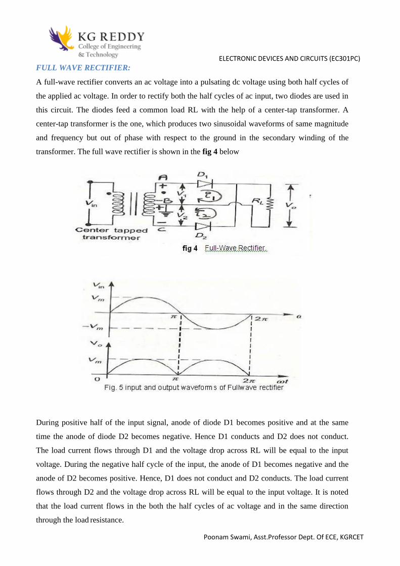
FULL WAVE RECTIFIER:
A full-wave rectifier converts an ac voltage into a pulsating dc voltage using both half cycles of
the applied ac voltage. In order to rectify both the half cycles of ac input, two diodes are used in
this circuit. The diodes feed a common load RL with the help of a center-tap transformer. A
center-tap transformer is the one, which produces two sinusoidal waveforms of same magnitude
and frequency but out of phase with respect to the ground in the secondary winding of the
transformer. The full wave rectifier is shown in the fig 4 below
During positive half of the input signal, anode of diode D1 becomes positive and at the same
time the anode of diode D2 becomes negative. Hence D1 conducts and D2 does not conduct.
The load current flows through D1 and the voltage drop across RL will be equal to the input
voltage. During the negative half cycle of the input, the anode of D1 becomes negative and the
anode of D2 becomes positive. Hence, D1 does not conduct and D2 conducts. The load current
flows through D2 and the voltage drop across RL will be equal to the input voltage. It is noted
that the load current flows in the both the half cycles of ac voltage and in the same direction
through the load resistance.

ELECTRONIC DEVICES AND CIRCUITS (EC301PC)
Poonam Swami, Asst.Professor Dept. Of ECE, KGRCET
5. BRIDGE RECTIFIER.
Another type of circuit that produces the same output waveform as the full wave rectifier
circuit above, is that of the Full Wave Bridge Rectifier. This type of single phase rectifier uses
four individual rectifying diodes connected in a closed loop "bridge" configuration to produce
the desired output. The main advantage of this bridge circuit is that it does not require a special
centre tapped transformer, thereby reducing its size and cost. The single secondary winding is
connected to one side of the diode bridge network and the load to the other side as shown below.
The Diode Bridge Rectifier
The four diodes labelled D1 to D4 are arranged in "series pairs" with only two diodes conducting
current during each half cycle. During the positive half cycle of the supply, diodes D1 and D2
conduct in series while diodes D3 and D4 are reverse biased and the current flows through the
load as shown below (fig 7).
The Positive Half-cycle

ELECTRONIC DEVICES AND CIRCUITS (EC301PC)
Poonam Swami, Asst.Professor Dept. Of ECE, KGRCET
The Negative Half-cycle
During the negative half cycle of the supply, diodes D3 and D4 conduct in series (fig 8), but
diodes D1 and D2 switch "OFF" as they are now reverse biased. The current flowing through
the load is the same direction as before.
As the current flowing through the load is unidirectional, so the voltage developed across the
load is also unidirectional the same as for the previous two diode full-wave rectifier, therefore
the average DC
Voltage across the load is 0.637Vmax. However in reality, during each half cycle the current
flows through two diodes instead of just one so the amplitude of the output voltage is two
voltage drops ( 2 x 0.7 = 1.4V ) less than the input VMAX amplitude. The ripple frequency is now
twice the supply frequency (e.g. 100Hz for a 50Hz supply)

ELECTRONIC DEVICES AND CIRCUITS (EC301PC)
Poonam Swami, Asst.Professor Dept. Of ECE, KGRCET
Unit2: BIPOLAR JUNCTION TRANSISTOR
1. CONSTRUCTION OF BJT AND ITS SYMBOLS
The Bipolar Transistor basic construction consists of two PN-junctions producing three
connecting terminals with each terminal being given a name to identify it from the other two.
These three terminals are known and labelled as the Emitter ( E ), the Base ( B ) and the
Collector ( C ) respectively. There are two basic types of bipolar transistor construction, PNP
and NPN, which basically describes the physical arrangement of the P-type and N-type
semiconductor materials from which they are made.
Transistors are three terminal active devices made from different semiconductor materials that
can act as either an insulator or a conductor by the application of a small signal voltage. The
transistor's ability to change between these two states enables it to have two basic functions:
"switching" (digital electronics) or "amplification" (analogue electronics). Then bipolar
transistors have the ability to operate within three different regions:
1. Active Region - the transistor operates as an amplifier and Ic = β.Ib
2. Saturation - the transistor is "fully-ON" operating as a switch and Ic = I(saturation)
3. Cut-off - the transistor is "fully-OFF" operating as a switch and Ic = 0
Bipolar Transistors are current regulating devices that control the amount of current flowing
through them in proportion to the amount of biasing voltage applied to their base terminal acting
like a current-controlled switch. The principle of operation of the two transistor types PNP and
NPN, is exactly the same the only difference being in their biasing and the polarity of the power
supply for each type(fig 1).

ELECTRONIC DEVICES AND CIRCUITS (EC301PC)
Poonam Swami, Asst.Professor Dept. Of ECE, KGRCET
Fig 3.1 Bipolar Junction Transistor Symbol
The construction and circuit symbols for both the PNP and NPN bipolar transistor are given
above with the arrow in the circuit symbol always showing the direction of "conventional
current flow" between the base terminal and its emitter terminal. The direction of the arrow
always points from the positive P-type region to the negative N-type region for both transistor
types, exactly the same as for the standard diode symbol
2. COMMON-BASE CONFIGURATION
Common-base terminology is derived from the fact that the : base is common to both input and
output of t configuration. base is usually the terminal closest to or at ground potential. Majority
carriers can cross the reverse-biased junction because the injected majority carriers will appear
as minority carriers in the n-type material.

ELECTRONIC DEVICES AND CIRCUITS (EC301PC)
Poonam Swami, Asst.Professor Dept. Of ECE, KGRCET
All current directions will refer to conventional (hole) flow and the arrows in all electronic
symbols have a direction defined by this convention. Note that the applied biasing (voltage
sources) are such as to establish current in the direction indicated for each branch.
Fig 3.4 CB Configuration
To describe the behavior of common-base amplifiers requires two set of characteristics:
1. Input or driving point characteristics.
2. Output or collector characteristics
The output characteristics have 3 basic regions:
• Active region –defined by the biasing arrangements
• Cutoff region – region where the collector current is 0A
• Saturation region- region of the characteristics to the left of VCB = 0V

ELECTRONIC DEVICES AND CIRCUITS (EC301PC)
Poonam Swami, Asst.Professor Dept. Of ECE, KGRCET
The curves (output characteristics) clearly indicate that a first approximation to the relationship
between IE and IC in the active region is given by IC ≈IE Once a transistor is in the ‘on’ state,
the base-emitter voltage will be assumed to beVBE = 0.7V
In the dc mode the level of IC and IE due to the majority carriers are related by a quantity called
alpha
= αdc
IC = IE + ICBO
It can then be summarize to IC = IE (ignore ICBO due to small value)
For ac situations where the point of operation moves on the characteristics curve, an ac alpha
defined by αac Alpha a common base current gain factor that shows the efficiency by calculating
the current percent from current flow from emitter to collector. The value of is typical from
0.9 ~ 0.998.

ELECTRONIC DEVICES AND CIRCUITS (EC301PC)
Poonam Swami, Asst.Professor Dept. Of ECE, KGRCET
3. TRANSISTOR AS AN AMPLIFIER
Common-Emitter Configuration
It is called common-emitter configuration since : emitter is common or reference to both input
and output terminals.emitter is usually the terminal closest to or at ground potential. Almost
amplifier design is using connection of CE due to the high gain for current and voltage. Two set
of characteristics are necessary to describe the behavior for CE ;input (base terminal) and output
(collector terminal) parameters. Proper Biasing common-emitter configuration in active region
IB is microamperes compared to miliamperes of IC.
IB will flow when VBE > 0.7V for silicon and 0.3V for germanium Before this value IB is very
small and no IB. Base-emitter junction is forward bias Increasing VCE will reduce IB for
different values.

ELECTRONIC DEVICES AND CIRCUITS (EC301PC)
Poonam Swami, Asst.Professor Dept. Of ECE, KGRCET
Fig 3.9a Input characteristics for common-emitter npn transistor
Fig 3.9b Output characteristics for common-emitter npn transistor

ELECTRONIC DEVICES AND CIRCUITS (EC301PC)
Poonam Swami, Asst.Professor Dept. Of ECE, KGRCET
For small VCE (VCE < VCESAT, IC increase linearly with increasing of VCE VCE > VCESAT IC not
totally depends on VCE constant IC
IB(uA) is very small compare to IC (mA). Small increase in IB cause big increase in IC IB=0 A
ICEO occur.
Noticing the value when IC=0A. There is still some value of current flows.
4 . METHODS OF TRANSISTOR BIASING
1) Fixed bias (base bias)

ELECTRONIC DEVICES AND CIRCUITS (EC301PC)
Poonam Swami, Asst.Professor Dept. Of ECE, KGRCET
Fig 4.3 Fixed Biasing Circuit
This form of biasing is also called base bias. In the fig 4.3 shown, the single power source (for
example, battery) is used for both collector and base of a transistor, although separate batteries
can also be used.
In the given circuit, Vcc = IBRB + Vbe
Therefore, IB = (Vcc - Vbe)/RB
Since the equation is independent of current ICR, dIB//dICR =0 and the stability factor is given
by the equation….. reduces to
S=1+β
Since β is a large quantity, this is very poor biasing circuit. Therefore in practice the circuit is not
used fo biasing.
For a given transistor, Vbe does not vary significantly during use. As Vcc is of fixed value, on selection of R the base current IB is fixed. Therefore this type is called fixed bias type of circuit.
Also for given circuit, Vcc = ICRC + Vce
Therefore, Vce = Vcc - ICRC
Merits:
• It is simple to shift the operating point anywhere in the active region by
merely changing the base resistor (RB).
• A very small number of components are required.
Demerits:
• The collector current does not remain constant with variation in temperature
or power supply voltage. Therefore the operating point is unstable.
• Changes in Vbe will change IB and thus cause RE to change. This in turn will
alter the gain of the stage.
• When the transistor is replaced with another one, considerable change in the
value of β can be expected. Due to this change the operating point will shift.

ELECTRONIC DEVICES AND CIRCUITS (EC301PC)
Poonam Swami, Asst.Professor Dept. Of ECE, KGRCET
5. EMITTER-FEEDBACK BIAS:
The emitter feedback bias circuit is shown in the fig 4.4. The fixed bias circuit is
modified by attaching an external resistor to the emitter. This resistor introduces negative
feedback that stabilizes the Q-point. From Kirchhoff's voltage law, the voltage across the base
resistor is
VRb = VCC - IeRe - Vbe.
Fig 4.4 Self Biasing Circuit
From Ohm's law, the base current is
Ib = VRb / Rb.
The way feedback controls the bias point is as follows. If Vbe is held constant and temperature
increases, emitter current increases. However, a larger Ie increases the emitter voltage Ve = IeRe,
which in turn reduces the voltage VRb across the base resistor. A lower base-resistor voltage
drop reduces the base current, which results in less collector current because Ic = ß IB. Collector
current and emitter current are related by Ic = α Ie with α ≈ 1, so increase in emitter current with
temperature is opposed, and operating point is kept stable.
Similarly, if the transistor is replaced by another, there may be a change in IC (corresponding to
change in β-value, for example). By similar process as above, the change is negated and
operating point kept stable.
For the given circuit,
IB = (VCC - Vbe)/(RB + (β+1)RE).
ELECTRONIC DEVICES AND CIRCUITS (EC301PC)
Poonam Swami, Asst.Professor Dept. Of ECE, KGRCET
Merits:
The circuit has the tendency to stabilize operating point against changes in temperature and β-
value.
Demerits:
• In this circuit, to keep IC independent of β the following condition must be
met:
which is approximately the case if ( β + 1 )RE >> RB.
• As β-value is fixed for a given transistor, this relation can be satisfied either by keeping RE very large, or making RB very low.
• If RE is of large value, high VCC is necessary. This increases cost as well as
precautions necessary while handling.
• If RB is low, a separate low voltage supply should be used in the base circuit.
Using two supplies of different voltages is impractical. • In addition to the above, RE causes ac feedback which reduces the
voltage gain of the amplifier.
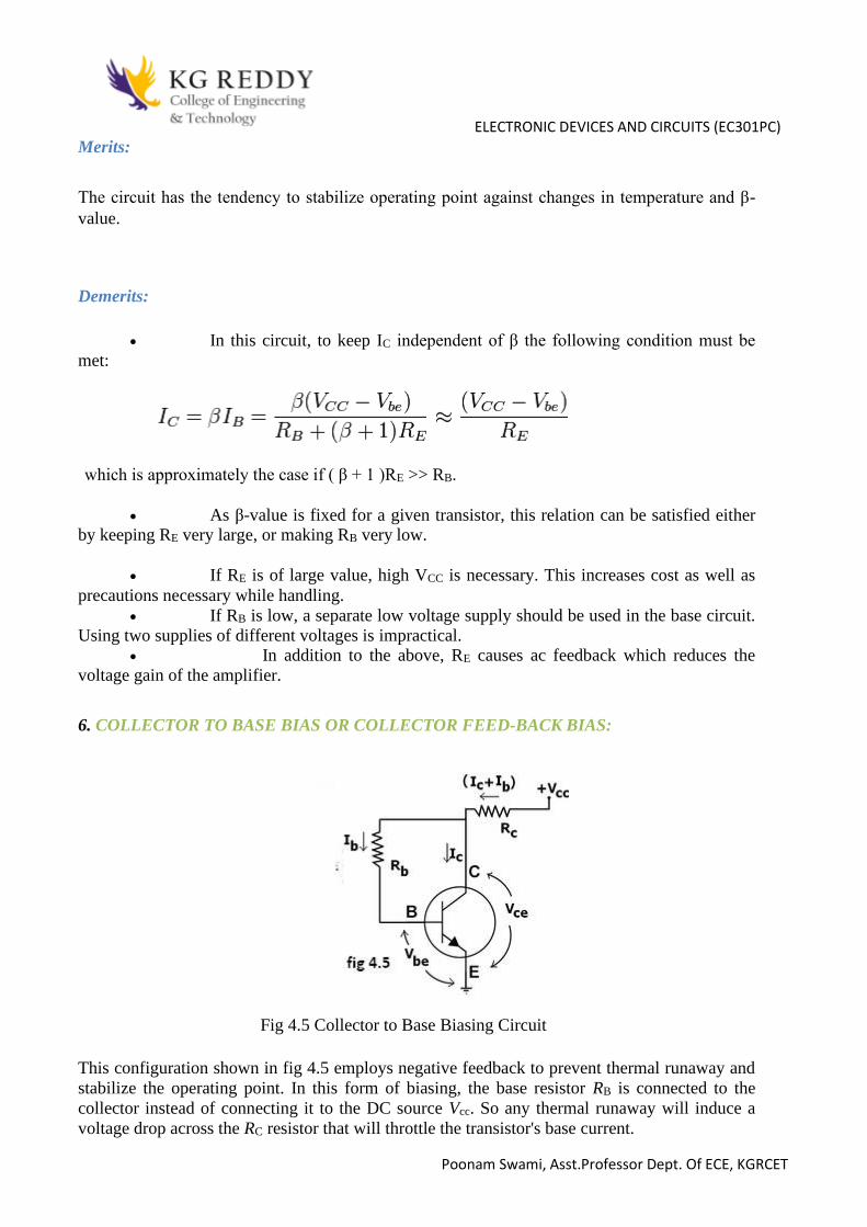
6. COLLECTOR TO BASE BIAS OR COLLECTOR FEED-BACK BIAS:
Fig 4.5 Collector to Base Biasing Circuit
This configuration shown in fig 4.5 employs negative feedback to prevent thermal runaway and
stabilize the operating point. In this form of biasing, the base resistor RB is connected to the
collector instead of connecting it to the DC source Vcc. So any thermal runaway will induce a
voltage drop across the RC resistor that will throttle the transistor's base current.

ELECTRONIC DEVICES AND CIRCUITS (EC301PC)
Poonam Swami, Asst.Professor Dept. Of ECE, KGRCET
From Kirchhoff's voltage law, the voltage across the base resistor Rb is
By the Ebers–Moll model, Ic = βIb, and so
From Ohm's law, the base current , and so
Hence, the base current Ib is
If Vbe is held constant and temperature increases, then the collector current Ic increases.
However, a larger Ic causes the voltage drop across resistor Rc to increase, which in turn reduces
the
voltage across the base resistor Rb. A lower base-resistor voltage drop reduces the base
current Ib, which results in less collector current Ic. Because an increase in collector current with
temperature is opposed, the operating point is kept stable.
Merits:
• Circuit stabilizes the operating point against variations in temperature and β
(i.e. replacement of transistor)
Demerits:
• In this circuit, to keep Ic independent of β, the following condition must be met:

ELECTRONIC DEVICES AND CIRCUITS (EC301PC)
Poonam Swami, Asst.Professor Dept. Of ECE, KGRCET
which is the case when
• As β-value is fixed (and generally unknown) for a given transistor, this relation can be satisfied either by keeping Rc fairly large or making Rb very low.
• If Rc is large, a high Vcc is necessary, which increases cost as well as
precautions necessary while handling.
• If Rb is low, the reverse bias of the collector–base region is small, which
limits the range of collector voltage swing that leaves the transistor in active mode.
• The resistor Rb causes an AC feedback, reducing the voltage gain of the
amplifier. This undesirable effect is a trade-off for greater Q-point stability.
Usage: The feedback also decreases the input impedance of the amplifier as seen from
the base, which can be advantageous. Due to the gain reduction from feedback, this biasing form
is used only when the trade-off for stability is warranted.

ELECTRONIC DEVICES AND CIRCUITS (EC301PC)
Poonam Swami, Asst.Professor Dept. Of ECE, KGRCET
Unit3: JUNCTION FIELD EFFECT TRANSISTOR
1. ZENER DIODES
The Zener diode is like a general-purpose signal diode consisting of a silicon PN junction.
When biased in the forward direction it behaves just like a normal signal diode passing the rated
current, but as soon as a reverse voltage applied across the zener diode exceeds the rated voltage
of the device, the diodes breakdown voltage VB is reached at which point a process called
Avalanche Breakdown occurs in the semiconductor depletion layer and a current starts to flow
through the diode to limit this increase in voltage.
The current now flowing through the zener diode increases dramatically to the maximum circuit
value (which is usually limited by a series resistor) and once achieved this reverse saturation
current remains fairly constant over a wide range of applied voltages. This breakdown voltage
point, VB is called the "zener voltage" for zener diodes and can range from less than one volt to
hundreds of volts.
The point at which the zener voltage triggers the current to flow through the diode can be very
accurately controlled (to less than 1% tolerance) in the doping stage of the diodes semiconductor
construction giving the diode a specific zener breakdown voltage, (Vz) for example, 4.3V or
7.5V. This zener breakdown voltage on the I-V curve is almost a vertical straight line.
Fig 1.19: Zener diode characteristics

ELECTRONIC DEVICES AND CIRCUITS (EC301PC)
Poonam Swami, Asst.Professor Dept. Of ECE, KGRCET
Zener Diode I-V Characteristics
The Zener Diode is used in its "reverse bias" or reverse breakdown mode, i.e. the diodes anode
connects to the negative supply. From the I-V characteristics curve above, we can see that the
zener diode has a region in its reverse bias characteristics of almost a constant negative voltage
regardless of the value of the current flowing through the diode and remains nearly constant
even with large changes in current as long as the zener diodes current remains between the
breakdown current IZ(min) and the maximum current rating IZ(max).
This ability to control itself can be used to great effect to regulate or stabilize a voltage source
against supply or load variations. The fact that the voltage across the diode in the breakdown
region is almost constant turns out to be an important application of the zener diode as a voltage
regulator. The function of a regulator is to provide a constant output voltage to a load connected
in parallel with it in spite of the ripples in the supply voltage or the variation in the load current
and the zener diode will continue to regulate the voltage until the diodes current falls below the
minimum IZ(min) value in the reverse breakdown region.
2 . PRINCIPLE OF OPERATION OF SCR
A silicon-controlled rectifier (or semiconductor-controlled rectifier) is a four-layer solid
state device that controls current. The name "silicon controlled rectifier" or SCR is General
Electric's trade name for a type of thyristor. The SCR was developed by a team of power
engineers led by Gordon Hall and commercialized by Frank W. "Bill" Gutzwiller in
1957.symbol of SCR is given below:
Fig 1.22: symbol of SCR
Construction of SCR
An SCR consists of four layers of alternating P and N type semiconductor materials. Silicon is
used as the intrinsic semiconductor, to which the proper dopants are added. The junctions are
either diffused or alloyed. The planar construction is used for low power SCRs (and all the
junctions are diffused). The mesa type construction is used for high power SCRs. In this case,
junction J2 is obtained by the diffusion method and then the outer two layers are alloyed to it,
since the PNPN pellet is required to handle large currents. It is properly braced with tungsten or
molybdenum plates to provide greater mechanical strength. One of these plates is hard soldered
to a copper stud, which is threaded for attachment of heat sink. The doping of PNPN will

ELECTRONIC DEVICES AND CIRCUITS (EC301PC)
Poonam Swami, Asst.Professor Dept. Of ECE, KGRCET
depend on the application of SCR, since its characteristics are similar to those of the thyratron.
Today, the term thyristor applies to the larger family of multilayer devices that exhibit bistable
state-change behaviour, that is, switching either ON or OFF.
The operation of a SCR and other thyristors can be understood in terms of a pair of tightly
coupled bipolar junction transistors, arranged to cause the self-latching action.The following
figures are construction of SCR,its two transistor model and symbol respectively
Fig 1.23: Construction, Two transistor model of SCR and symbol of SCR
SCR Working Principle
Fig 1.24: Current flow and voltage bias in an SCR
The SCR is a four-layer, three-junction and a three-terminal device and is shown in fig.1.24.
The end P- region is the anode, the end N-region is the cathode and the inner P-region is the
gate. The anode to cathode is connected in series with the load circuit. Essentially the device is a
switch. Ideally it remains off (voltage blocking state), or appears to have an infinite impedance
until both the anode and gate terminals have suitable positive voltages with respect to the
cathode terminal. The thyristor then switches on and current flows and continues to conduct
without further gate signals. Ideally the thyristor has zero impedance in conduction state. For
switching off or reverting to the blocking state, there must be no gate signal and the anode
current must be reduced to zero. Current can flow only in one direction.
In absence of external bias voltages, the majority carrier in each layer diffuses until there is a
built-in voltage that retards further diffusion. Some majority carriers have enough energy to
cross the barrier caused by the retarding electric field at each junction. These carriers then
become minority carriers and can recombine with majority carriers. Minority carriers in each
layer can be accelerated across each junction by the fixed field, but because of absence of
external circuit in this case the sum of majority and minority carrier currents must be zero.

ELECTRONIC DEVICES AND CIRCUITS (EC301PC)
Poonam Swami, Asst.Professor Dept. Of ECE, KGRCET
A voltage bias, as shown in figure, and an external circuit to carry current allow internal currents which include the following terms:
The current Ix is due to
• Majority carriers (holes) crossing junction J1
• Minority carriers crossing junction J1
• Holes injected at junction J2 diffusing through the N-region and crossing junction J1 and
• Minority carriers from junction J2 diffusing through the N-region and crossing junction J1.
V I characteristics of SCR:
Fig 1.25: V-I characteristics of SCR

ELECTRONIC DEVICES AND CIRCUITS (EC301PC)
Poonam Swami, Asst.Professor Dept. Of ECE, KGRCET
As already mentioned, the SCR is a four-layer device with three terminals, namely, the anode,
the cathode and the gate. When the anode is made positive with respect to the cathode, junctions
J1 and J3 are forward biased and junction J2 is reverse-biased and only the leakage current will
flow through the device. The SCR is then said to be in the forward blocking state or in the
forward mode or off state. But when the cathode is made positive with respect to the anode,
junctions J1 and J3 are reverse-biased, a small reverse leakage current will flow through the SCR
and the SGR is said to be in the reverse blocking state or in reverse mode.
When the anode is positive with respect to cathode i.e. when the SCR is in forward mode, the
SCR does not conduct unless the forward voltage exceeds certain value, called the forward
breakover voltage, VFB0. In non-conducting state, the current through the SCR is the leakage
current which is very small and is negligible. If a positive gate current is supplied, the SCR can
become conducting at a voltage much lesser than forward break-over voltage. The larger the
gate current, lower the break-over voltage. With sufficiently large gate current, the SCR behaves
identical to PN rectifier. Once the SCR is switched on, the forward voltage drop across it is
suddenly reduced to very small value, say about 1 volt. In the conducting or on-state, the current
through the SCR is limited by the external impedance.
When the anode is negative with respect to cathode, that is when the SCR is in reverse mode or
in blocking state no current flows through the SCR except very small leakage current of the
order of few micro-amperes, but if the reverse voltage is increased beyond a certain value,
called the reverse break- over voltage, VRB0 avalanche break down takes place. Forward break-
over voltage VFB0 is usually higher than reverse breakover voltage,VRBO.
From the foregoing discussion, it can be seen that the SCR has two stable and reversible
operating states. The change over from off-state to on-state, called turn-on, can be achieved by
increasing the forward voltage beyond VFB0. A more convenient and useful method of turn-on
the device employs the gate drive. If the forward voltage is less than the forward break-over
voltage, VFB0, it can be turned-on by applying a positive voltage between the gate and the
cathode. This method is called the gate control. Another very important feature of the gate is
that once the SCR is triggered to on-state the gate loses its control.
The switching action of gate takes place only when
(i) SCR is forward biased i.e. anode is positive with respect to cathode, and
(ii) Suitable positive voltage is applied between the gate and the cathode.
Once the SCR has been switched on, it has no control on the amount of current flowing
through it. The current through the SCR is entirely controlled by the external impedance
connected in the circuit and the applied voltage. There is, however, a very small, about 1 V,
potential drop across the SCR. The forward current through the SCR can be reduced by reducing
the applied voltage or by increasing the circuit impedance. There is, however, a minimum
forward current that must be maintained to keep the SCR in conducting state. This is called the
holding current rating of SCR. If the current through the SCR is reduced below the level of
holding current, the device returns to off-state or blocking state.

ELECTRONIC DEVICES AND CIRCUITS (EC301PC)
Poonam Swami, Asst.Professor Dept. Of ECE, KGRCET
The SCR can be switched off by reducing the forward current below the level of holding current which may be done either by reducing the applied voltage or by increasing the circuit
impedance.
Note : The gate can only trigger or switch-on the SCR, it cannot switch off.
Alternatively the SCR can be switched off by applying negative voltage to the anode (reverse
mode), the SCR naturally will be switched off.
Here one point is worth mentioning, the SCR takes certain time to switch off. The time, called
the turn- off time, must be allowed before forward voltage may be applied again otherwise the
device will switch-on with forward voltage without any gate pulse. The turn-off time is about 15
micro-seconds, which is immaterial when dealing with power frequency, but this becomes
important in the inverter circuits, which are to operate at high frequency.
Merits of SCR
1. Very small amount of gate drive is required.
2. SCRs with high voltage and current ratings are available.
3. On state losses of SCR are less.
Demerits of SCR
1. Gate has no control, once SCR is turned on.
2. External circuits are required for turning it off.
3. Operationg frequencies are low.
4. Additional protection circuits are required.
Application of SCRs
SCRs are mainly used in devices where the control of high power, possibly coupled with high
voltage, is demanded. Their operation makes them suitable for use in medium to high-voltage
AC power control applications, such as lamp dimming, regulators and motor control.
3. CONSTRUCTION AND OPERATION OF N- CHANNEL FET
If the gate is an N-type material, the channel must be a P-type material.
CONSTRUCTION OF N-CHANNEL JFET

ELECTRONIC DEVICES AND CIRCUITS (EC301PC)
Poonam Swami, Asst.Professor Dept. Of ECE, KGRCET
Fig 5.2 Construction of N-Channel JFET
A piece of N- type material, referred to as channel has two smaller pieces of P-type
material attached to its sides, forming PN junctions. The channel ends are designated as the
drain and source. And the two pieces of P-type material are connected together and their
terminal is called the gate. Since this channel is in the N-type bar, the FET is known as N-
channel JFET.
OPERATION OF N-CHANNEL JFET:-
The overall operation of the JFET is based on varying the width of the channel to control the
drain current.
A piece of N type material referred to as the channel, has two smaller pieces of P type
material attached to its sites, farming PN –Junctions. The channel’s ends are designated the
drain and the source. And the two pieces of P type material are connected together and their
terminal is called the gate. With the gate terminal not connected and the potential applied
positive at the drain negative at the source a drain current Id flows. When the gate is biased
negative with respective to the source the PN junctions are reverse biased and depletion regions
are formed. The channel is more lightly doped than the P type gate blocks, so the depletion
regions penetrate deeply into the channel. Since depletion region is a region depleted of charge
carriers it behaves as an Insulator. The result is that the channel is narrowed. Its resistance is
increased and Id is reduced. When the negative gate bias voltage is further increased, the
depletion regions meet at the center and Id is cut off completely.

ELECTRONIC DEVICES AND CIRCUITS (EC301PC)
Poonam Swami, Asst.Professor Dept. Of ECE, KGRCET
There are two ways to control the channel width
1. By varying the value of Vgs
2. And by Varying the value of Vds holding Vgs constant
1 By varying the value of Vgs :-
We can vary the width of the channel and in turn vary the amount of drain current. This can
be done by varying the value of Vgs. This point is illustrated in the fig below. Here we are
dealing with N channel FET. So channel is of N type and gate is of P type that constitutes a PN
junction. This PN junction is always reverse biased in JFET operation .The reverse bias is
applied by a battery voltage Vgs connected between the gate and the source terminal i.e positive
terminal of the battery is connected to the source and negative terminal to gate.
1) When a PN junction is reverse biased the electrons and holes diffuse across junction by leaving
immobile ions on the N and P sides , the region containing these immobile ions is known as
depletion regions.
2) If both P and N regions are heavily doped then the depletion region extends symmetrically on
both sides.
3) But in N channel FET P region is heavily doped than N type thus depletion region extends more
in N region than P region.

ELECTRONIC DEVICES AND CIRCUITS (EC301PC)
Poonam Swami, Asst.Professor Dept. Of ECE, KGRCET
4) So when no Vds is applied the depletion region is symmetrical and the conductivity becomes
Zero. Since there are no mobile carriers in the junction.
5) As the reverse bias voltage is increases the thickness of the depletion region also increases. i.e.
the effective channel width decreases .
6) By varying the value of Vgs we can vary the width of the channel.
2 Varying the value of Vds holding Vgs constant :-
1) When no voltage is applied to the gate i.e. Vgs=0 , Vds is applied between source and drain the
electrons will flow from source to drain through the channel constituting drain current Id .
2) With Vgs= 0 for Id= 0 the channel between the gate junctions is entirely open .In response to a
small applied voltage Vds , the entire bar acts as a simple semi conductor resistor and the
current Id increases linearly with Vds .
3) The channel resistances are represented as rd and rs as shown in the fig.
4) This increasing drain current Id produces a voltage drop across rd which reverse biases the gate
to source junction,(rd> rs) .Thus the depletion region is formed which is not symmetrical .
5) The depletion region i.e. developed penetrates deeper in to the channel near drain and less
towards source because Vrd >> Vrs. So reverse bias is higher near drain than at source.
6) As a result growing depletion region reduces the effective width of the channel. Eventually a
voltage Vds is reached at which the channel is pinched off. This is the voltage where the current
Id begins to level off and approach a constant value.
7) So, by varying the value of Vds we can vary the width of the channel holding Vgs constant.

ELECTRONIC DEVICES AND CIRCUITS (EC301PC)
Poonam Swami, Asst.Professor Dept. Of ECE, KGRCET
When both Vgs and Vds is applied:-
It is of course in principle not possible for the channel to close Completely and there by
reduce the current Id to Zero for, if such indeed, could be the case the gate voltage Vgs is
applied in the direction to provide additional reverse bias
1) When voltage is applied between the drain and source with a battery Vdd, the electrons flow
from source to drain through the narrow channel existing between the depletion regions. This
constitutes the drain current Id, its conventional direction is from drain to source.
2) The value of drain current is maximum when no external voltage is applied between gate and
source and is designated by Idss.

ELECTRONIC DEVICES AND CIRCUITS (EC301PC)
Poonam Swami, Asst.Professor Dept. Of ECE, KGRCET
3) When Vgs is increased beyond Zero the depletion regions are widened. This reduces the
effective width of the channel and therefore controls the flow of drain current through the
channel.
4) When Vgs is further increased a stage is reached at which to depletion regions touch each other
that means the entire channel is closed with depletion region. This reduces the drain current to
Zero.
4. E-MOSFETS
The E MOSFET is capable of operating only in the enhancement mode.The gate potential must
be positive w.r.t to source.
1) when the value of Vgs=0V, there is no channel connecting the source and drain materials.
2) As aresult , there can be no significant amount of drain current.
3) When Vgs=0, the Vdd supply tries to force free electrons from source to drain but the
presence of p-region does not permit the electrons to pass through it. Thus there is no drain
current at Vgs=0,
4) If Vgs is positive, it induces a negative charge in the p type substrate just adjacent to the
SIO2 layer.
5) As the holes are repelled by the positive gate voltage, the minority carrier electrons attracted
toward this voltage. This forms an effective N type bridge between source and drain providing
a path for drain current.
6) This +ve gate voltage forma a channel between the source and drain.
7) This produces a thin layer of N type channel in the P type substarate.This layer of free
electrons is called N type inversion layer.

ELECTRONIC DEVICES AND CIRCUITS (EC301PC)
Poonam Swami, Asst.Professor Dept. Of ECE, KGRCET
8) The minimum Vgs which produces this inversion layer is called threshold voltage
and is designated by Vgs(th).This is the point at which the device turns on is called the threshold
voltage Vgs(th)
9)When the voltage Vgs is <Vgs (th) no current flows from drain to source.
10)How ever when the voltage Vgs > Vgs (th) the inversion layer connects the drain to source
and we get significant values of current.
5. Common Source (CS) Amplifier
Fig. 5.1 (a) CS Amplifier (b) Small-signal equivalent circuit
A simple Common Source amplifier is shown in Fig. 5.1(a) and associated small signal
equivalent circuit using voltage-source model of FET is shown in Fig. 5.1(b)

ELECTRONIC DEVICES AND CIRCUITS (EC301PC)
Poonam Swami, Asst.Professor Dept. Of ECE, KGRCET
Voltage Gain
Source resistance (RS) is used to set the Q-Point but is bypassed by CS for mid-frequency
operation. From the small signal equivalent circuit ,the output voltage
VO = -RDµVgs(RD + rd)
Where Vgs = Vi , the input voltage, Hence, the voltage gain,
AV = VO / Vi = -RDµ(RD + rd)
Input Impedence
From Fig. 5.1(b) Input Impedence is Zi = RG
For voltage divider bias as in CE Amplifiers of BJT
RG = R1 ║ R2
Output Impedance
Output impedance is the impedance measured at the output terminals with the input voltage VI =
0 From the Fig. 5.1(b) when the input voltage Vi = 0, Vgs = 0 and hence
µ Vgs = 0
The equivalent circuit for calculating output impedence is given in Fig. 5.2. Output impedence
Zo = rd ║ RD
Normally rd will be far greater than RD . Hence Zo ≈ RD
6. Common Drain Amplifier
A simple common drain amplifier is shown in Fig. 5.2(a) and associated small signal
equivalent circuit using the voltage source model of FET is shown in Fig. 5.2(b).Since voltage
Vgd is more easily determined than Vgs, the voltage source in the output circuit is expressed in
terms of Vgs and Thevenin’s theorem.
Fig. 5.2 (a)CD Amplifier (b)Small-signal equivalent circuit

ELECTRONIC DEVICES AND CIRCUITS (EC301PC)
Poonam Swami, Asst.Professor Dept. Of ECE, KGRCET
Voltage Gain
The output voltage,
VO = RSµVgd / (µ + 1) RS + rd Where Vgd = Vi the input voltage. Hence, the voltage gain,
Av = VO / Vi = RSµ / (µ + 1) RS + rd
Input Impedence
From Fig. 5.2(b), Input Impedence Zi = RG
Output Impedence
From Fig. 5.2(b), Output impedence measured at the output terminals with input voltage Vi =
0 can be calculated from the following equivalent circuit.
As Vi = 0: Vgd = 0: µvgd / (µ + 1) = 0 Output Impedence
ZO = rd / (µ + 1) ║RS
When µ » 1
ZO = ( rd / µ) ║RS = (1/gm) ║RS
6. VOLTAGE DIVIDER BIAS FET:-
The fig5.6 shows N channel JFET with voltage divider bias. The voltage at the source of JFET
must be more positive than the voltage at the gate in order to keep the gate to source junction
reverse biased. The source voltage is
VS = IDRS
The gate voltage is set by resistors R1 and R2 as expressed by the following equation using
the voltage divider formula.

ELECTRONIC DEVICES AND CIRCUITS (EC301PC)
Poonam Swami, Asst.Professor Dept. Of ECE, KGRCET
Vg= Vdd
For dc analysis fig 5.5
Applying KVL to the input circuit VG-VGS-VS =0
:: VGS = VG-Vs=VG-ISRS VGS = VG-IDRS :: IS = ID
Applying KVL to the input circuit we get VDS+IDRD+VS-VDD =0
::VDS = VDD-IDRD-IDRS VDS = VDD-ID ( RD +RS )
The Q point of a JFET amplifier, using the voltage divider bias is IDQ = IDSS [1-VGS/VP]2
VDSQ = VDD-ID (RD+RS)

ELECTRONIC DEVICES AND CIRCUITS (EC301PC)
Poonam Swami, Asst.Professor Dept. Of ECE, KGRCET
Unit4: ANALYSIS AND DESIGN OF SMALL SIGNAL LOW
FREQUENCY BJT AMPLIFER
1. BJT HYBRID MODEL
Small signal low frequency transistor Models:
All the transistor amplifiers are two port networks having two voltages and two currents. The positive directions of voltages and currents are shown in fig. 1.
Fig. 1
A two-port network is represented by four external variables: voltage V1 and current I1 at the
input port, and voltage V2 and current I2 at the output port, so that the two-port network can be
treated as a black box modeled by the relationships between the four variables,V1,V2, I1,I2 .
Out of four variables two can be selected as are independent variables and two are dependent
variables.The dependent variables can be expressed interns of independent variables. This
leads to various two port parameters out of which the following three are important:
1. Impedance parameters (z-parameters)
2. Admittance parameters (y-parameters)
3. Hybrid parameters (h-parameters)
z-parameters
A two-port network can be described by z-parameters as
In matrix form, the above equation can be rewritten as

ELECTRONIC DEVICES AND CIRCUITS (EC301PC)
Poonam Swami, Asst.Professor Dept. Of ECE, KGRCET
Where
Input impedance with output port open circuited
Reverse transfer impedance with input port open circuited
Forward transfer impedance with output port open circuited
Output impedance with input port open circuited
Y-parameters
A two-port network can be described by Y-parameters as
In matrix form, the above equation can be rewritten as

ELECTRONIC DEVICES AND CIRCUITS (EC301PC)
Poonam Swami, Asst.Professor Dept. Of ECE, KGRCET
Input admittance with output port short circuited
Reverse transfer admittance with input port short circuited
Forward transfer admittance with output port short circuited
Output admittance with input port short circuited
Hybrid parameters (h-parameters)
If the input current I1 and output voltage V2 are taken as independent variables, the dependent
variables V1 and I2 can be written as
Where h11, h12, h21, h22 are called as hybrid parameters.
Input impedence with o/p port short circuited
Reverse voltage transfer ratio with i/p port open circuited

ELECTRONIC DEVICES AND CIRCUITS (EC301PC)
Poonam Swami, Asst.Professor Dept. Of ECE, KGRCET
Forward voltage transfer ratio with o/p port short circuited
output impedence with i/p port open circuited THE HYBRID MODEL FOR TWO PORT
NETWORK:
Based on the definition of hybrid parameters the mathematical model for two pert networks
known as h-parameter model can be developed. The hybrid equations can be written as:
(The following convenient alternative subscript notation is recommended by the IEEE
Standards:
i=11= input o = 22 = output
f =21 = forward transfer r = 12 = reverse transfer)
We may now use the four h parameters to construct a mathematical model of the device of
Fig.(1). The hybrid circuit for any device indicated in Fig.(2). We can verify that the model of
Fig.(2) satisfies above equations by writing Kirchhoff'svoltage and current laws for input and
output ports.

ELECTRONIC DEVICES AND CIRCUITS (EC301PC)
Poonam Swami, Asst.Professor Dept. Of ECE, KGRCET
If these parameters are specified for a particular configuration, then suffixes e,b or c are also
included,
e.g. hfe ,h ib are h parameters of common emitter and common collector amplifiers
Using two equations the generalized model of the amplifier can be drawn as shown in fig. 2.
Fig. 2
2. ANALYSIS OF A TRANSISTOR AMPLIFIER USING H-PARAMETERS:
To form a transistor amplifier it is only necessary to connect an external load and signal
source as indicated in fig. 1 and to bias the transistor properly.
Fig. 1
Consider the two-port network of CE amplifier. RS is the source resistance and ZL is the load
impedence h-parameters are assumed to be constant over the operating range. The ac
equivalent circuit is shown in fig. 2. (Phasor notations are used assuming sinusoidal voltage
input). The quantities of interest are the current gain, input impedence, voltage gain, and
output impedence.

ELECTRONIC DEVICES AND CIRCUITS (EC301PC)
Poonam Swami, Asst.Professor Dept. Of ECE, KGRCET
Current gain:
For the transistor amplifier stage, Ai is defined as the ratio of output to input currents.
Input impedence:
The impedence looking into the amplifier input terminals ( 1,1' ) is the input impedance Zi
Voltage gain: The ratio of output voltage to input voltage gives the gain of the transistors.
Output Admittance

ELECTRONIC DEVICES AND CIRCUITS (EC301PC)
Poonam Swami, Asst.Professor Dept. Of ECE, KGRCET
It is defined as
Av is the voltage gain for an ideal voltage source (Rv = 0).
Consider input source to be a current source IS in parallel with a resistance RS as shown in fig.
3.
Fig. 3
In this case, overall current gain AIS is defined as

ELECTRONIC DEVICES AND CIRCUITS (EC301PC)
Poonam Swami, Asst.Professor Dept. Of ECE, KGRCET
Unit5: FET AMPLIFIER
1. Explain the FET small signal model.
The linear small signal equivalent circuit for the FET can be obtained in a manner similar to
that used to derive the corresponding model for a transistor.
We can express the drain current iD as a function f of the gate voltage and drain voltage Vds. Id
=f(Vgs,Vds) -------------------------------- (1)
The transconductance gm and drain resistance rd:-
If both gate voltage and drain voltage are varied, the change in the drain current is
approximated by using taylors series considering only the first two terms in the expansion
∆id= |vds=constant .∆vgs |vgs=constant∆vds we can write ∆id=id
∆vgs=vgs
∆vds=vds
Id=gm v Vds→(1)
Where gm= |Vds |Vds
gm= |Vds
Is the mutual conductance or transconductance .It is also called as gfs or yfs common source
forward conductance .
The second parameter rd is the drain resistance or output resistance is defined as
rd= |Vgs |Vgs= |Vgs rd= |Vgs
The reciprocal of the rd is the drain conductance gd .It is also designated by Yos and Gos and
called the common source output conductance . So the small signal equivalent circuit for FET
can be drawn in two different ways.
1. small signal current –source model 2.small signal voltage-source model.
A small signal current –source model for FET in common source configuration can be drawn

ELECTRONIC DEVICES AND CIRCUITS (EC301PC)
Poonam Swami, Asst.Professor Dept. Of ECE, KGRCET
satisfying Eq→(1) as shown in the figure(a)
This low frequency model for FET has a Norton’s output circuit with a dependent current
generator whose magnitude is proportional to the gate-to –source voltage. The proportionality
factor is the transconductance ‘gm’. The output resistance is ‘rd’. The input resistance between
the gate and source is infinite, since it is assumed that the reverse biased gate draws no
current. For the same reason the resistance between gate and drain is assumed to be infinite.
The small signal voltage-source model is shown in the figure(b).
This can be derived by finding the Thevenin’s equivalent for the output part of fig(a) .
These small signal models for FET can be used for analyzing the three basic FET amplifier
configurations:
1.common source (CS) 2.common drain (CD) or source follower
3. common gate(CG).
(a)Small Signal Current source model for FET (b)Small Signal voltage source model
for FET
Here the input circuit is kept open because of having high input impedance and the output
circuit satisfies the equation for ID
2. Explain the working of E-MOSFET.
The E MOSFET is capable of operating only in the enhancement mode.The gate potential
must be positive w.r.t to source.

ELECTRONIC DEVICES AND CIRCUITS (EC301PC)
Poonam Swami, Asst.Professor Dept. Of ECE, KGRCET
when the value of Vgs=0V, there is no channel connecting the source and drain materials.
As aresult , there can be no significant amount of drain current.
When Vgs=0, the Vdd supply tries to force free electrons from source to drain but the presence
of p-region does not permit the electrons to pass through it. Thus there is no drain current at
Vgs=0,
If Vgs is positive, it induces a negative charge in the p type substrate just adjacent to the SIO2
layer.
As the holes are repelled by the positive gate voltage, the minority carrier electrons attracted
toward this voltage. This forms an effective N type bridge between source and drain providing a
path for drain current.
This +ve gate voltage forma a channel between the source and drain.
This produces a thin layer of N type channel in the P type substarate.This layer of free electrons
is called N type inversion layer.
The minimum Vgs which produces this inversion layer is called threshold voltage and is
designated by Vgs(th).This is the point at which the device turns on is called the threshold
voltage Vgs(th)
When the voltage Vgs is <Vgs (th) no current flows from drain to source.

ELECTRONIC DEVICES AND CIRCUITS (EC301PC)
Poonam Swami, Asst.Professor Dept. Of ECE, KGRCET
How ever when the voltage Vgs > Vgs (th) the inversion layer connects the drain to source and
we get significant values of current.
2. Draw and explain the common source amplifier.
Common Source (CS) Amplifier
Fig. 5.1 (a) CS Amplifier (b) Small-signal equivalent circuit
A simple Common Source amplifier is shown in Fig. 5.1(a) and associated small signal
equivalent circuit using voltage-source model of FET is shown in Fig. 5.1(b)
Voltage Gain
Source resistance (RS) is used to set the Q-Point but is bypassed by CS for mid-frequency
operation. From the small signal equivalent circuit ,the output voltage
VO = -RDµVgs(RD + rd)
Where Vgs = Vi , the input voltage, Hence, the voltage gain,
AV = VO / Vi = -RDµ(RD + rd)
Input Impedence
From Fig. 5.1(b) Input Impedence is Zi = RG
For voltage divider bias as in CE Amplifiers of BJT
RG = R1 ║ R2
Output Impedance
Output impedance is the impedance measured at the output terminals with the input voltage VI =
0 From the Fig. 5.1(b) when the input voltage Vi = 0, Vgs = 0 and hence
µ Vgs = 0
The equivalent circuit for calculating output impedence is given in Fig. 5.2. Output impedence
Zo = rd ║ RD Normally rd will be far greater than RD . Hence Zo ≈ RD
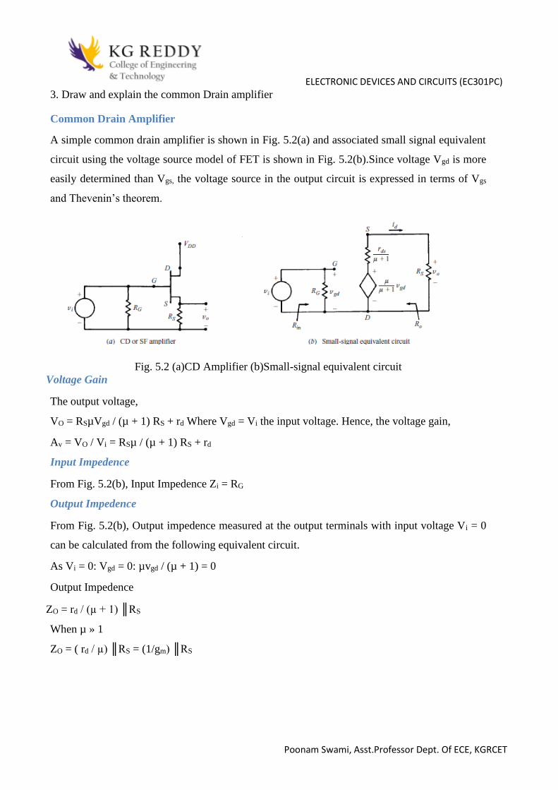
ELECTRONIC DEVICES AND CIRCUITS (EC301PC)
Poonam Swami, Asst.Professor Dept. Of ECE, KGRCET
3. Draw and explain the common Drain amplifier
Common Drain Amplifier
A simple common drain amplifier is shown in Fig. 5.2(a) and associated small signal equivalent
circuit using the voltage source model of FET is shown in Fig. 5.2(b).Since voltage Vgd is more
easily determined than Vgs, the voltage source in the output circuit is expressed in terms of Vgs
and Thevenin’s theorem.
Fig. 5.2 (a)CD Amplifier (b)Small-signal equivalent circuit
Voltage Gain
The output voltage,
VO = RSµVgd / (µ + 1) RS + rd Where Vgd = Vi the input voltage. Hence, the voltage gain,
Av = VO / Vi = RSµ / (µ + 1) RS + rd
Input Impedence
From Fig. 5.2(b), Input Impedence Zi = RG
Output Impedence
From Fig. 5.2(b), Output impedence measured at the output terminals with input voltage Vi = 0
can be calculated from the following equivalent circuit.
As Vi = 0: Vgd = 0: µvgd / (µ + 1) = 0
Output Impedence
ZO = rd / (µ + 1) ║RS
When µ » 1
ZO = ( rd / µ) ║RS = (1/gm) ║RS

ELECTRONIC DEVICES AND CIRCUITS (EC301PC)
Poonam Swami, Asst.Professor Dept. Of ECE, KGRCET
14) Tutorial topics and Questions
• Rectifiers
• Transistor biasing
• Biasing of FET
• Special Purpose diodes
• Analysis of CE
• Low frequency response of BJT amplifier
• Analysis of FET amplifier

ELECTRONIC DEVICES AND CIRCUITS (EC301PC)
Poonam Swami, Asst.Professor Dept. Of ECE, KGRCET
15) Unit Wise Question Bank:
Unit1
1. Two marks questions with answer
1.What is a pn junction? How is it formed?
In a piece of sc, if one half is doped by p type impurity and the other half is doped by n type impurity, a
PN junction is formed. The plane dividing the two halves or zones is called PN junction. As shown in
the fig the n type material has high concentration of free electrons, while p type material has high
concentration of holes.
Fig : Symbol of PN Junction Diode
2. Write the application of pn diode
Can be used as rectifier in DC Power Supplies.
In Demodulation or Detector Circuits.
In clamping networks used as DC Restorers
In clipping circuits used for waveform generation.
As switches in digital logic circuits.
In demodulation circuits.
3. What is barrier potential?
Because of the oppositely charged ions present on both sides of PN junction an electric potential is
established across the junction even without any external voltage source which is termed as barrier
potential.
4 . What is rectifier?
Any electrical device which offers a low resistance to the current in one direction but a high
resistance to the current in the opposite direction is called rectifier. Such a device is capable of
converting a sinusoidal input waveform, whose average value is zero, into a unidirectional Waveform,
with a non- zero average component. A rectifier is a device, which converts a.c. voltage (bi-directional)
to pulsating voltage (Unidirectional).

ELECTRONIC DEVICES AND CIRCUITS (EC301PC)
Poonam Swami, Asst.Professor Dept. Of ECE, KGRCET
5 .Define Effective (or) R.M.S current:
The effective (or) R.M.S. current squared ofa periodic function of time is given by the area of one
cycle of the curve, which represents the square of the function divided by the base.
6. what are the disadvantages of half wave rectifier.
The ripple factor is high.
The efficiency is low.
The Transformer Utilization factor is low.
2. Three marks question with answers
1. What is avalanche break down?
When bias is applied, thermally generated carriers which are already present in the diode acquire
sufficient energy from the applied potential to produce new carriers by removing valence electron from
their bonds. These newly generated additional carriers acquire more energy from the potential and they
strike the lattice and create more number of free electrons and holes. This process goes on as long as
bias is increased and the number of free carriers gets multiplied. This process is termed as avalanche
multiplication. Thus the break down which occurs in the junction resulting in heavy flow of current is
termed as avalanche break down.
2. Explain the effect of temperature on the V-I characteristics of pn junction diode.
Temperature can have a marked effect on the characteristics of a silicon semiconductor diode as shown
in Fig. 11 It has been found experimentally that the reverse saturation current Io will just about double
in magnitude for every 10°C increase in temperature
6
Fig 1.11 Variation in Diode Characteristics with temperature change
Vrms = 0
2 1 T
T V d (wt)

ELECTRONIC DEVICES AND CIRCUITS (EC301PC)
Poonam Swami, Asst.Professor Dept. Of ECE, KGRCET
It is not uncommon for a germanium diode with an Io in the order of 1 or 2 A at 25°C to have a leakage
current of 100 A - 0.1 mA at a temperature of 100°C. Typical values of Io for silicon are much lower
than that of germanium for similar power and current levels. The result is that even at high
temperatures the levels of Io for silicon diodes do not reach the same high levels obtained. For
germanium—a very important reason that silicon devices enjoy a significantly higher level of
development and utilization in design. Fundamentally, the open-circuit equivalent in the reverse bias
region is better realized at any temperature with silicon than with germanium. The increasing levels of
Io with temperature account for the lower levels of threshold voltage, as shown in Fig. 1.11. Simply
increase the level of Io in and not rise in diode current. Of course, the level of TK also will be increase,
but the increasing level of Io will overpower the smaller percent change in TK. As the temperature
increases the forward characteristics are actually becoming more “ideal,”
3. What are the advantages and disadvantages of full wave rectifier.
Advantages
1) Ripple factor = 0.482 (against 1.21 for HWR)
2) Rectification efficiency is 0.812 (against 0.405 for HWR)
3) Better TUF (secondary) is 0.574 (0.287 for HWR)
4) No core saturation problem
Disadvantages:
1) Requires center tapped transformer.
4 .Define i) ripple factor and Peak Inverse Voltage (PIV)
i) Ripple Factor :
It is defined as ration of R.M.S. value of a.c. component to the d.c. component in the output is known
as “Ripple Factor”.
ii) Peak Inverse Voltage (PIV):
It is defined as the maximum reverse voltage that a diode can withstand without destroying the
junction.
5 Disadvantages of half-wave rectifier:
1. The ripple factor is high.

ELECTRONIC DEVICES AND CIRCUITS (EC301PC)
Poonam Swami, Asst.Professor Dept. Of ECE, KGRCET
2. The efficiency is low.
3. The Transformer Utilization factor is low.
6. What is full wave rectifier
A full-wave rectifier converts an ac voltage into a pulsating dc voltage using both half cycles of the
applied ac voltage. In order to rectify both the half cycles of ac input, two diodes are used in this
circuit. The diodes feed a common load RL with the help of a center-tap transformer. A center-tap
transformer is the one, which produces two sinusoidal waveforms of same magnitude and frequency
but out of phase with respect to the ground in the secondary winding of the transformer.
1. Five marks question answers
1. Explain the operation of PN junction under forward bias condition with its characteristics
When a diode is connected in a Forward Bias condition, a negative voltage is applied to the N- type
material and a positive voltage is applied to the P-type material. If this external voltage becomes
greater than the value of the potential barrier, approx. 0.7 volts for silicon and 0.3 volts for germanium,
the potential barriers opposition will be overcome and current will start to flow. This is because the
negative voltage pushes or repels electrons towards the junction giving them the energy to cross over
and combine with the holes being pushed in the opposite direction towards the junction by the positive
voltage. This results in a characteristics curve of zero current flowing up to this voltage point, called the
"knee" on the static curves and then a high current flow through the diode with little increase in the
external voltage as shown below.
Forward Characteristics Curve for a Junction Diode

ELECTRONIC DEVICES AND CIRCUITS (EC301PC)
Poonam Swami, Asst.Professor Dept. Of ECE, KGRCET
Fig 1.8a: Diode Forward Characteristics
The application of a forward biasing voltage on the junction diode results in the depletion layer
becoming very thin and narrow which represents a low impedance path through the junction thereby
allowing high currents to flow. The point at which this sudden increase in current takes place is
represented on the static I-V characteristics curve above as the "knee" point.
Forward Biased Junction Diode showing a Reduction in the Depletion Layer
Fig 1.8b: Diode Forward Bias
This condition represents the low resistance path through the PN junction allowing very large currents
to flow through the diode with only a small increase in bias voltage. The actual potential difference
across the junction or diode is kept constant by the action of the depletion layer at approximately 0.3v
for germanium and approximately 0.7v for silicon junction diodes. Since the diode can conduct
"infinite" current above this knee point as it effectively becomes a short circuit, therefore resistors are
used in series with the diode to limit its current flow. Exceeding its maximum forward current
specification causes the device to dissipate more power in the form of heat than it was designed for
resulting in a very quick failure of the device.
2. Explain the operation of Half Wave Rectifier.
A Half – wave rectifier as shown in fig 1.2 is one, which converts a.c. voltage into a pulsating voltage
using only one half cycle of the applied a.c. voltage.
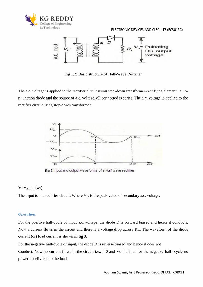
ELECTRONIC DEVICES AND CIRCUITS (EC301PC)
Poonam Swami, Asst.Professor Dept. Of ECE, KGRCET
Fig 1.2: Basic structure of Half-Wave Rectifier
The a.c. voltage is applied to the rectifier circuit using step-down transformer-rectifying element i.e., p-
n junction diode and the source of a.c. voltage, all connected is series. The a.c. voltage is applied to the
rectifier circuit using step-down transformer
V=Vm sin (wt)
The input to the rectifier circuit, Where Vm is the peak value of secondary a.c. voltage.
Operation:
For the positive half-cycle of input a.c. voltage, the diode D is forward biased and hence it conducts.
Now a current flows in the circuit and there is a voltage drop across RL. The waveform of the diode
current (or) load current is shown in fig 3.
For the negative half-cycle of input, the diode D is reverse biased and hence it does not
Conduct. Now no current flows in the circuit i.e., i=0 and Vo=0. Thus for the negative half- cycle no
power is delivered to the load.

ELECTRONIC DEVICES AND CIRCUITS (EC301PC)
Poonam Swami, Asst.Professor Dept. Of ECE, KGRCET
3. Explain about the Full Wave Rectifier
A full-wave rectifier converts an ac voltage into a pulsating dc voltage using both half cycles of the
applied ac voltage. In order to rectify both the half cycles of ac input, two diodes are used in this
circuit. The diodes feed a common load RL with the help of a center-tap transformer. A center-tap
transformer is the one, which produces two sinusoidal waveforms of same magnitude and frequency
but out of phase with respect to the ground in the secondary winding of the transformer. The full wave
rectifier is shown in the fig 4 below
During positive half of the input signal, anode of diode D1 becomes positive and at the same time the
anode of diode D2 becomes negative. Hence D1 conducts and D2 does not conduct. The load current
flows through D1 and the voltage drop across RL will be equal to the input voltage.
During the negative half cycle of the input, the anode of D1 becomes negative and the anode of D2
becomes positive. Hence, D1 does not conduct and D2 conducts. The load current flows through D2
and the voltage drop across RL will be equal to the input voltage. It is noted that the load current flows
in the both the half cycles of ac voltage and in the same direction through the load resistance.

ELECTRONIC DEVICES AND CIRCUITS (EC301PC)
Poonam Swami, Asst.Professor Dept. Of ECE, KGRCET
4. Explain the operation of BRIDGE RECTIFIER.
Another type of circuit that produces the same output waveform as the full wave rectifier circuit above,
is that of the Full Wave Bridge Rectifier. This type of single phase rectifier uses four individual
rectifying diodes connected in a closed loop "bridge" configuration to produce the desired output. The
main advantage of this bridge circuit is that it does not require a special centre tapped transformer,
thereby reducing its size and cost. The single secondary winding is connected to one side of the diode
bridge network and the load to the other side as shown below.
The Diode Bridge Rectifier
The four diodes labeled D1 to D4 are arranged in "series pairs" with only two diodes conducting current
during each half cycle. During the positive half cycle of the supply, diodes D1 and D2 conduct in series
while diodes D3 and D4 are reverse biased and the current flows through the load as shown below

ELECTRONIC DEVICES AND CIRCUITS (EC301PC)
Poonam Swami, Asst.Professor Dept. Of ECE, KGRCET
The Positive Half-cycle
The Negative Half-cycle
During the negative half cycle of the supply, diodes D3 and D4 conduct in series (fig 8), but diodes D1
and D2 switch "OFF" as they are now reverse biased. The current flowing through the load is the same
direction as before.
As the current flowing through the load is unidirectional, so the voltage developed across the load is
also unidirectional the same as for the previous two diode full-wave rectifier, therefore the average DC
voltage across the load is 0.637Vmax.However in reality, during each half cycle the current flows
through two diodes instead of just one so the amplitude of the output voltage is two voltage drops ( 2 x
0.7 = 1.4V ) less than the input VMAX amplitude. The ripple frequency is now twice the supply
frequency (e.g. 100Hz for a 50Hz supply.

ELECTRONIC DEVICES AND CIRCUITS (EC301PC)
Poonam Swami, Asst.Professor Dept. Of ECE, KGRCET
5. compare the HWR,FWR and BR.
Multiple Choice Questions:
Unit-1
1. In a PN junction with no external voltage, the electric field between acceptor and donor ions is
called a
A.Peak
B.Barrier
C.Threshold
D. Path
2. The capacitance of a reverse biased PN junction
A.Increases as reverse bias is increased
B.Decreases as reverse bias is increased
C.Increases as reverse bias is decreased
D.Is insignificantly low
3. For a P-N junction diode, the current in reverse bias may be
A.Few miliamperes
B.Between 0.2 A and 15 A
C.Few amperes
D.Few micro or nano amperes

ELECTRONIC DEVICES AND CIRCUITS (EC301PC)
Poonam Swami, Asst.Professor Dept. Of ECE, KGRCET
4 .For the same secondary voltage, the output voltage from a centre-tap rectifier is ………… than that
of bridge rectifier
A. twice
B. thrice
C. four time
D. one-half
5. A 10 V power supply would use …………………. as filter capacitor.
A. paper capacitor
B. mica capacitor
C. electrolytic capacitor
D. air capacitor
6. The maximum efficiency of a half-wave rectifier is ………………..
A. 40.6 %
B. 81.2 %
C. 50 %
D. 25 %
7. The most widely used rectifier is ……………….
A. half-wave rectifier
B. centre-tap full-wave rectifier
C. bridge full-wave rectifier
D. none of the above
8. The ripple factor of a half-wave rectifier is …………………
A. 2
B. 1.21
C. 2.5
D. 0.48
9.If the a.c. input to a half-wave rectifier is an r.m.s value of 400/√2 volts, then diode PIV rating is
………………….
A. 400/√2 V
B. 400 V
C. 400 x √2 V
D. none of the above

ELECTRONIC DEVICES AND CIRCUITS (EC301PC)
Poonam Swami, Asst.Professor Dept. Of ECE, KGRCET
10. The disadvantage of a half-wave rectifier is that the……………….
A. components are expensive
B. diodes must have a higher power rating
C. output is difficult to filter
D. none of the above
Fill in the blanks
1 .The ripple to heavy loads by a capacitor is_______
2. Number of diodes used in a full wave bridge rectifier is_________
3. Ripple factor of bridge full wave rectifier is?
4. Efficiency of a half wave rectifier is
5. There is a need of transformer for ………………..
6. What makes the load in a choke filter to bypass harmonic components?
7. DC average current of a bridge full wave rectifier (where Im is the maximum peak current of input).
8. Bridge rectifier is an alternative for
9.Transformer utilization factor of a centre tapped full wave rectifier is_________
10.The ……………….. Filter circuit results in the best voltage regulation
Solutions
MCQ’s Fill in the blanks
1. 1.B Low
2. 2.C 4
3. 3.D 0.482
4. 4.D 40.6%
5. 5.C centre-tap full-wave rectifier
6. 6.A Capacitor
7.C Im
7. 8.B Full wave rectifier
8. 9.B 0.693
9. 10.C choke input

ELECTRONIC DEVICES AND CIRCUITS (EC301PC)
Poonam Swami, Asst.Professor Dept. Of ECE, KGRCET
UNIT 2
1. Two marks question answers
1. Collector region of transistor is larger than emitter. Why?
Collector is made physically larger than emitter and base because collector is to dissipate much
power.
2. Why BJT is called current controlled device?
The output voltage, current, or power is controlled by the input current in a transistor. So it is called
the current controlled device.
3. Define Early Effect.
A variation of the base-collector voltage results in a variation of the quasi-neutral width in the base.
The gradient of the minority-carrier density in the base therefore changes, yielding an increased
collector current as the collector-base current is increased. This effect is referred to as the Early
effect.
4. Why h parameter model is important for BJT
It is important because:
1. its values are used on specification sheets
2. it is one model that may be used to analyze circuit behavior
3. it may be used to form the basis of a more accurate transistor model
5. Collector region of transistor is larger than emitter. Why?
Collector is made physically larger than emitter and base because collector is to dissipate much
power.
6. What are the types of biasing?
The following discussion treats five common biasing circuits used with class-A bipolar
transistor amplifiers:
• Fixed bias.
• Collector-to-base bias.
• Fixed bias with emitter resistor.
• Voltage divider bias or potential divider.
• Emitter bias.

ELECTRONIC DEVICES AND CIRCUITS (EC301PC)
Poonam Swami, Asst.Professor Dept. Of ECE, KGRCET
7. What is bias stabilization in transistor?
A transistor can work as amplifier, only if the dc/ac voltages and currents in the circuit are suitably
fixed. The operating point or bias point or quiescent point(or simply Q-point) is the voltage or
current which, when applied to a device, causes it to operate in a certain desired fashion. Need
for BIAS STABILIZATION.
8. What is thermal runway? How can it avoid?
The collector current for the CE circuit is given by The three variables in the equation, β, , and increases with rise in temperature. In particular, the reverse saturation current or leakage current changes greatly with temperature. Specifically it doubles for every 10oC rise in temperature. The collector current causes the collector base junction temperature to rise which in turn, increase , as a result will increase still further, which will further rise the temperature at the collector base junction. This process will become cumulative leading at the Collector base junction. This process will become cumulative leading to “thermal runaway”.
Consequently, the ratings of the transistor are exceeded which may destroy the transistor itself. The
collector is made larger in size than the emitter in order to help the heat developed at the collector
junction. However if the circuit is designed such that the base current is made to decrease
automatically with rise in temperature, then the decrease in will compensate for increase in the
, keeping almost constant.
9. What are the demerits of fixed bias?
Demerits:
• The collector current does not remain constant with variation in temperature or
power supply voltage. Therefore the operating point is unstable.
• Changes in Vbe will change IB and thus cause RE to change. This in turn will alter
the gain of the stage.
• When the transistor is replaced with another one, considerable change in the value
of β can be expected. Due to this change the operating point will shift.
10. What is Stability factor?
STABILITY FACTOR (S):
The rise of temperature results in increase in the value of transistor gain β and the leakage current
Ico. So, IC also increases which results in a shift in operating point. Therefore, The biasing network
should be provided with thermal stability. Maintenance of the operating point is specified by S,
which indicates the degree of change in operating point due to change in temperature.

ELECTRONIC DEVICES AND CIRCUITS (EC301PC)
Poonam Swami, Asst.Professor Dept. Of ECE, KGRCET
The extent to which IC is stabilized with varying IC is measured by a stability factor S
,
For CE configuration Differentiate the above equation w.r.t IC , We get
S should be small to have better thermal stability
2. Three marks question answers
1. Compare CE, CB, CC.
2. Define current amplification factor
In a transistor amplifier with a.c. input signal, the ratio of change in output current to be the change in
input current is known as the current amplification factor

ELECTRONIC DEVICES AND CIRCUITS (EC301PC)
Poonam Swami, Asst.Professor Dept. Of ECE, KGRCET
3. . Give some applications of BJT
The BJT remains a device that excels in some applications, such as discrete circuit design, due to the
very wide selection of BJT types available, and because of its high transconductance and output
resistance compared to MOSFETs. The BJT is also the choice for demanding analog circuits,
especially for very-high-frequency applications, such as radio-frequency circuits for wireless systems.
Bipolar transistors can be combined with MOSFETs in an integrated circuit by using a BiCMOS
process of wafer fabrication to create circuits that take advantage of the application strengths of both
types of transistor
4. Draw the characteristics of CB configuration.
5. Describe the working of bias compensation using diode & transistor.

ELECTRONIC DEVICES AND CIRCUITS (EC301PC)
Poonam Swami, Asst.Professor Dept. Of ECE, KGRCET
The various biasing circuits considered use some type of negative feedback to stabilize the operation
point. Also, diodes, thermistors and sensistors can be used to compensate for variations in current.
DIODE COMPENSATION:
The following fig4.8 shows a transistor amplifier with a diode D connected across the base- emitter
junction for compensation of change in collector saturation current ICO. The diode is of the same
material as the transistor and it is reverse biased by e the emitter-base junction voltage VBE, allowing
the diode reverse saturation current IO to flow through diode D. The base current IB=I-IO.
As long as temperature is constant, diode D operates as a resistor. As the temperature increases, ICO of
the transistor increases. Hence, to compensate for this, the base current IB should be decreased.
The increase in temperature will also cause the leakage current IO through D to increase and thereby decrease the base current IB. This is the required action to keep Ic constant.
This type of bias compensation does not need a change in Ic to effect the change in IC, as both IO and ICO can track almost equally according to the change in temperature.
THERMISTOR COMPENSATION:
The following fig4.9 a thermistor RT, having a negative temperature coefficient is connected in
parallel with R2. The resistance of thermistor decreases exponentially with increase of temperature.
An increase of temperature will decrease the base voltage VBE, reducing IB and IC.

ELECTRONIC DEVICES AND CIRCUITS (EC301PC)
Poonam Swami, Asst.Professor Dept. Of ECE, KGRCET
Fig 4.9 Thermistor Compensation
SENSISTOR COMPENSATION:
In the following fig4.10 shown a sensistor Rs having a positive temperature coefficient is connected
across R1 or RE. Rs increases with temperature. As the temperature increases, the equivalent resistance
of the parallel combination of R1 and Rs also increases and hence VBE decreases, reducing IB and Ic.
This reduced Ic compensates for increased Ic caused by the increase in VBE, ICO and β due to
temperature.
Fig 4.10 Sensistor Compensation

ELECTRONIC DEVICES AND CIRCUITS (EC301PC)
Poonam Swami, Asst.Professor Dept. Of ECE, KGRCET
Five marks question answers
1. Explain the input and output characteristics of a transistor in CB configuration.
Common-base terminology is derived from the fact that the : base is common to both input and output
of t configuration. base is usually the terminal closest to or at ground potential. Majority carriers can
cross the reverse-biased junction because the injected majority carriers will appear as minority carriers
in the n-type material. All current directions will refer to conventional (hole) flow and the arrows in all
electronic symbols have a direction defined by this convention.
Note that the applied biasing (voltage sources) are such as to establish current in the direction indicated
for each branch.
Fig 3.4 CB Configuration
To describe the behavior of common-base amplifiers requires two set of characteristics:
1. Input or driving point characteristics.
2. Output or collector characteristics
The output characteristics has 3 basic regions:
• Active region –defined by the biasing arrangements
• Cutoff region – region where the collector current is 0A
• Saturation region- region of the characteristics to the left of VCB = 0V

ELECTRONIC DEVICES AND CIRCUITS (EC301PC)
Poonam Swami, Asst.Professor Dept. Of ECE, KGRCET
Fig 3.5 CB Input-Output Characteristics
The curves (output characteristics) clearly indicate that a first approximation to the relationship
between IE and IC in the active region is given by
IC ≈IE
Once a transistor is in the ‘on’ state, the base-emitter voltage will be assumed to beVBE = 0.7V

ELECTRONIC DEVICES AND CIRCUITS (EC301PC)
Poonam Swami, Asst.Professor Dept. Of ECE, KGRCET
In the dc mode the level of IC and IE due to the majority carriers are related by a quantity called alpha
= αdc
IC = IE + ICBO
It can then be summarize to IC = IE (ignore ICBO due to small value)
For ac situations where the point of operation moves on the characteristics curve, an ac alpha defined
by αac
Alpha a common base current gain factor that shows the efficiency by calculating the current percent
from current flow from emitter to collector. The value of is typical from 0.9 ~ 0.998.
2. With neat sketches and necessary waveforms explain the input and output characteristics of a
BJT in CE configuration. Also derive expression for output current.
It is called common-emitter configuration since: emitter is common or reference to both input and
output terminals. Emitter is usually the terminal closest to or at ground potential.
Almost amplifier design is using connection of CE due to the high gain for current and voltage.
Two set of characteristics are necessary to describe the behavior for CE ;input (base terminal) and
output (collector terminal) parameters.
Proper Biasing common-emitter configuration in active region

ELECTRONIC DEVICES AND CIRCUITS (EC301PC)
Poonam Swami, Asst.Professor Dept. Of ECE, KGRCET
Fig 3.8 CE Configurations
IB is microamperes compared to miliamperes of IC.
IB will flow when VBE > 0.7V for silicon and 0.3V for germanium Before this value IB is very small
and no IB.
Base-emitter junction is forward bias Increasing VCE will reduce IB for different values.
Fig 3.9a Input characteristics for common-emitter npn transistor

ELECTRONIC DEVICES AND CIRCUITS (EC301PC)
Poonam Swami, Asst.Professor Dept. Of ECE, KGRCET
Fig 3.9b Output characteristics for common-emitter npn transistor
For small VCE (VCE < VCESAT, IC increase linearly with increasing of VCE VCE > VCESAT IC not totally
depends on VCE constant IC
IB(uA) is very small compare to IC (mA). Small increase in IB cause big increase in IC IB=0 A ICEO
occur.
Noticing the value when IC=0A. There is still some value of current flows.

ELECTRONIC DEVICES AND CIRCUITS (EC301PC)
Poonam Swami, Asst.Professor Dept. Of ECE, KGRCET
3. Voltage divider bias or self bias or emitter bias
The voltage divider as shown in the fig 4.7 is formed using external resistors R1 and R2. The voltage
across R2 forward biases the emitter junction. By proper selection of resistors R1 and R2, the
operating point of the transistor can be made independent of β. In this circuit, the voltage divider
holds the base voltage fixed independent of base current provided the divider current is large
compared to the base current. However, even with a fixed base voltage, collector current varies with
temperature (for example) so an emitter resistor is added to stabilize the Q-point, similar to the above
circuits with emitter resistor.
Fig 4.7 Voltage Divider Biasing Circuit
In this circuit the base voltage is given by:
voltage across
provided .
Also
For the given circuit,
ELECTRONIC DEVICES AND CIRCUITS (EC301PC)
Poonam Swami, Asst.Professor Dept. Of ECE, KGRCET
Let the current in resistor R1 is I1 and this is divided into two parts – current through base and
resistor R2. Since the base current is very small so for all practical purpose it is assumed that I1 also
flows through R2, so we have
Applying KVL in the circuit, we have
It is apparent from above expression that the collector current is independent of ? thus the stability is
excellent. In all practical cases the value of VBE is quite small in comparison to the V2, so it can be
ignored in the above expression so the collector current is almost independent of the transistor
parameters thus this arrangement provides excellent stability.
Again applying KVL in collector circuit, we have
The resistor RE provides stability to the circuit. If the current through the collector rises, the
voltage across the resistor RE also rises. This will cause VCE to increase as the voltage V2 is
independent of collector current. This decreases the base current, thus collector current increases to
its former value.
Stability factor for such circuit arrangement is given by

ELECTRONIC DEVICES AND CIRCUITS (EC301PC)
Poonam Swami, Asst.Professor Dept. Of ECE, KGRCET
If Req/RE is very small compared to 1, it can be ignored in the above expression thus we have
Which is excellent since it is the smallest possible value for the stability. In actual practice the
value of stability factor is around 8-10, since Req/RE cannot be ignored as compared to 1.
4. Explain the DC and AC load line.
DC LOAD LINE
Referring to the biasing circuit of fig 4.2a, the values of VCC and RC are fixed and Ic and VCE are
dependent on RB.
Applying Kirchhoff’s voltage law to the collector circuit in fig. 4.2a, we get
Fig 4.2a CE Amplifier circuit (b) Load line
The straight line represented by AB in fig4.2b is called the dc load line. The coordinates of the end
point A are obtained by substituting VCE =0 in the above equation. Then . Therefore
The coordinates of A are VCE =0 and .

ELECTRONIC DEVICES AND CIRCUITS (EC301PC)
Poonam Swami, Asst.Professor Dept. Of ECE, KGRCET
The coordinates of B are obtained by substituting Ic=0 in the above equation. Then Vce = Vcc.
Therefore the coordinates of B are VCE =Vcc and Ic=0. Thus the dc load line AB can be drawn if the
values of Rc and Vcc are known. As shown in the fig4.2b, the optimum POINT IS LOCATED AT
THE MID POINT OF THE MIDWAY BETWEEN a AND b. In order to get faithful amplification,
the Q point must be well within the active region of the transistor Even though the Q point is fixed
properly, it is very important to ensure that the operating point remains stable where it is originally
fixed. If the Q point shifts nearer to either A or B, the output voltage and current get clipped, thereby
o/p signal is distorted.
In practice, the Q-point tends to shift its position due to any or all of the following three main
factors..
1) Reverse saturation current, Ico, which doubles for every 10oC raise in temperature
2) Base emitter Voltage ,VBE, which decreases by 2.5 mV per oC
3) Transistor current gain, hFE or β which increases with temperature.
If base current IB is kept constant since IB is approximately equal to Vcc/RB. If the transistor is
replaced by another one of the same type, one cannot ensure that the new transistor will have
identical parameters as that of the first one. Parameters such as β vary over a range. This results in
the variation of collector current Ic for a given IB. Hence , in the o/p characteristics, the spacing
between the curves might increase or decrease which leads to the shifting of the Q-point to a location
which might be completely unsatisfactory.
AC LOAD LINE
After drawing the dc load line, the operating point Q is properly located at the center of the dc
load line. This operating point is chosen under zero input signal condition of the circuit. Hence the ac
load line should also pas through the operating point Q. The effective ac load resistance Rac, is a
combination of RC parallel to RL i.e. || . So the slope of the ac load line CQD will be
. To draw the ac load line, two end points, I.e. VCE(max) and IC(max) when the signal is applied are
required.
, which locates point D on the Vce axis.
, which locates the point C on the IC axis.
By joining points c and D, ac load line CD is constructed. As RC > Rac, The dc load line is less steep
than ac load line.

ELECTRONIC DEVICES AND CIRCUITS (EC301PC)
Poonam Swami, Asst.Professor Dept. Of ECE, KGRCET
5. Explain the working of fixed bias.
1) Fixed bias (base bias)
Fig 4.3 Fixed Biasing Circuit
This form of biasing is also called base bias. In the fig 4.3 shown, the single power source (for example, battery) is used for both collector and base of a transistor, although separate batteries can also
be used.
In the given circuit, Vcc = IBRB + Vbe
Therefore, IB = (Vcc - Vbe)/RB
Since the equation is independent of current ICR, dIB//dICR =0 and the stability factor is given by the
equation….. reduces to
S=1+β
Since β is a large quantity, this is very poor biasing circuit. Therefore in practice the circuit is not used
fo biasing.
For a given transistor, Vbe does not vary significantly during use. As Vcc is of fixed value, on selection
of R the base current IB is fixed. Therefore this type is called fixed bias type of circuit.
Also for given circuit, Vcc = ICRC + Vce
Therefore, Vce = Vcc - ICRC

ELECTRONIC DEVICES AND CIRCUITS (EC301PC)
Poonam Swami, Asst.Professor Dept. Of ECE, KGRCET
Merits:
• It is simple to shift the operating point anywhere in the active region by merely
changing the base resistor (RB).
• A very small number of components are required.
Demerits:
• The collector current does not remain constant with variation in temperature or
power supply voltage. Therefore the operating point is unstable.
• Changes in Vbe will change IB and thus cause RE to change. This in turn will alter
the gain of the stage.
• When the transistor is replaced with another one, considerable change in the value
of β can be expected. Due to this change the operating point will shift.
2.Explain the operation of emitter feedback bias.
The emitter feedback bias circuit is shown in the fig 4.4. The fixed bias circuit is modified by
attaching an external resistor to the emitter. This resistor introduces negative feedback that stabilizes
the Q-point. From Kirchhoff's voltage law, the voltage across the base resistor is
VRb = VCC - IeRe - Vbe.
Fig 4.4 Self Biasing Circuit
From Ohm's law, the base current is
Ib = VRb / Rb.
The way feedback controls the bias point is as follows. If Vbe is held constant and temperature
increases, emitter current increases. However, a larger Ie increases the emitter voltage Ve = IeRe,

ELECTRONIC DEVICES AND CIRCUITS (EC301PC)
Poonam Swami, Asst.Professor Dept. Of ECE, KGRCET
which in turn reduces the voltage VRb across the base resistor. A lower base-resistor voltage drop
reduces the base current, which results in less collector current because Ic = ß IB. Collector current and
emitter current are related by Ic = α Ie with α ≈ 1, so increase in emitter current with temperature is
opposed, and operating point is kept stable.
Similarly, if the transistor is replaced by another, there may be a change in IC (corresponding to
change in β-value, for example). By similar process as above, the change is negated and operating
point kept stable.
For the given circuit,
IB = (VCC - Vbe)/(RB + (β+1)RE).
Merits:
The circuit has the tendency to stabilize operating point against changes in temperature and β-
value.
Demerits:
• In this circuit, to keep IC independent of β the following condition must be met:
which is approximately the case if ( β + 1 )RE >> RB.
• As β-value is fixed for a given transistor, this relation can be satisfied either by
keeping RE very large, or making RB very low.
• If RE is of large value, high VCC is necessary. This increases cost as well as
precautions necessary while handling.
• If RB is low, a separate low voltage supply should be used in the base circuit. Using
two supplies of different voltages is impractical.
• In addition to the above, RE causes ac feedback which reduces the voltage
gain of the amplifier.

ELECTRONIC DEVICES AND CIRCUITS (EC301PC)
Poonam Swami, Asst.Professor Dept. Of ECE, KGRCET
Multiple Choice Questions
1. Which operating region of BJT enables Emitter-base & Collector-base junctions to undergo perfect
short-circuit configuration ?
a. Active Region
b. Saturation Region
c. Cut-off Region
d. None of the above
2. The total emitter current (IE) is given by_________
a) IE = IpE * InE
b) IE = IpE – InE
c) IE = IpE / InE
d) IE = IpE + InE
3. The grown junction type transistors is generally used for_________
a) PNP transistors
b) NPN transistors
c) Both transistors
d) depends on the material used
4. The relation between α and β is_________
a) β = α/ (1-α)
b) α = β/(1+β)
c) β = α/ (1+α)
d) α = β/(1- β)
5. When the signal is applied, the ratio of change of collector current to the ratio of change of base
current is called_________
a) dc current gain
b) base current amplification factor
c) emitter current amplification factor
d) ac current gain
6. Which of the following cases damage the transistor?
a) when VCE is increased too far
b) when VCE is decreased too far
c) when VBE is increased too far
d) when VBE is decreased too far

ELECTRONIC DEVICES AND CIRCUITS (EC301PC)
Poonam Swami, Asst.Professor Dept. Of ECE, KGRCET
7. A transistor has an IC of 100mA and IB of 0.5mA. What is the value of αdc?
a) 0.787
b) 0.995
c) 0.543
d) 0.659
8. The AC current gain in a common base configuration is_________
a) -∆IC/∆IE
b) ∆IC/∆IE
c) ∆IE/∆IC
d) -∆IE/∆IC
9. the output resistance of CB transistor is given by _________
a) ∆VCB/∆IC
b) ∆VBE/∆IB
c) ∆VBE/∆IC
d) ∆VEB/∆IE
10. The thermal runway is avoided in a self bias because_________
a) of its independence of β
b) of the positive feedback produced by the emitter resistor
c) of the negative feedback produced by the emitter resistor
d) of its dependence of β
Fill in the blanks
1.When transistors are used in digital circuits they usually operate in the:
2. In a C-E configuration, an emitter resistor is used for
3. The input resistance of the base of an emitter-follower is usually _________
4. VCE approximately equals ________ when a transistor switch is cut off.
5. An emitter-follower has a voltage gain that is __________.
6. VCE approximately equals ________ when a transistor switch is in saturation.
7. The phase difference between the input and output ac voltage signals of a common-emitter amplifier
is __________.

ELECTRONIC DEVICES AND CIRCUITS (EC301PC)
Poonam Swami, Asst.Professor Dept. Of ECE, KGRCET
8. A current ratio of IC/IE is usually less than one and is called:
9. The C-B configuration is used to provide which type of gain?
10. A transistor may be used as a switching device or as a:
Solutions
MCQ’s Fill in the blanks
1.B Saturation and cutoff regions
7 2.D 1. Stabilization
8 3.B 2. Very high
9 4.B VCC
10 5.D Approximately equal to one
11 6.A 3. 0.3V
12 7.B 4. 180º
8.A Alpha
9.A Voltage
10.C Variable resistor

ELECTRONIC DEVICES AND CIRCUITS (EC301PC)
Poonam Swami, Asst.Professor Dept. Of ECE, KGRCET
Unit 3
Two marks question answers
1. Give the advantages and disadvantages of tunnel diode
Advantages
1. Low noise
2. Ease of operation
3. High speed
4. Low power
Disadvantages
1. Voltage range over which it can be operated is 1 V less.
2. Being a two terminal device there is no isolation between the input and output circuit
2 What is photo diode?
The photo diode is a semiconductor p-n junction device whose region of operation is limited to
the reverse biased region. The figure below shows the symbol of photodiode
Fig :Symbol of photodiode.
3. Mention the applications of UJT.
1. It is used in timing circuits
2. It is used in switching circuits
3. It is used in phase control circuits
4. It can be used as trigger device for SCR and triac.
5. It is used in saw tooth generator.
6. It is used for pulse generation
4. Why do you call FET as field effect transistor?
The name “field effect” is derived from the fact that the current is controlled by an electric field set
up in the device by an external voltage, applied across gate and source terminals, which reverse bias
the junctions.
5. Define pinch off voltage?
It is the voltage at which the channel is pinched off, i.e. all the free charge from the channel get
removed. At Pinch-off voltage VP the drain current becomes constant.

ELECTRONIC DEVICES AND CIRCUITS (EC301PC)
Poonam Swami, Asst.Professor Dept. Of ECE, KGRCET
Three marks question answers
1. What is varactor diode?
A varactor diode is best explained as a variable capacitor. Think of the depletion region as a variable
dielectric. The diode is placed in reverse bias. The dielectric is “adjusted” by reverse bias voltage
changes.
• Junction capacitance is present in all reverse biased diodes because of the depletion region.
• Junction capacitance is optimized in a varactor diode and is used for high frequencies and switching
applications.
• Varactor diodes are often used for electronic tuning applications in FM radios and televisions
2. Draw the v-I characteristics of SCR
V I characteristics of SCR:
Fig 1.25: V-I characteristics of SCR

ELECTRONIC DEVICES AND CIRCUITS (EC301PC)
Poonam Swami, Asst.Professor Dept. Of ECE, KGRCET
As already mentioned, the SCR is a four-layer device with three terminals, namely, the anode, the
cathode and the gate. When the anode is made positive with respect to the cathode, junctions J1 and J3
are forward biased and junction J2 is reverse-biased and only the leakage current will flow through the
device. The SCR is then said to be in the forward blocking state or in the forward mode or off state.
But when the cathode is made positive with respect to the anode, junctions J1 and J3 are reverse-
biased, a small reverse leakage current will flow through the SCR and the SGR is said to be in the
reverse blocking state or in reverse mode.
When the anode is positive with respect to cathode i.e. when the SCR is in forward mode, the SCR
does not conduct unless the forward voltage exceeds certain value, called the forward breakover
voltage, VFB0. In non-conducting state, the current through the SCR is the leakage current which is
very small and is negligible. If a positive gate current is supplied, the SCR can become conducting at
a voltage much lesser than forward break-over voltage. The larger the gate current, lower the break-
over voltage. With sufficiently large gate current, the SCR behaves identical to PN rectifier. Once the
SCR is switched on, the forward voltage drop across it is suddenly reduced to very small value, say
about 1 volt. In the conducting or on-state, the current through the SCR is limited by the external
impedance. When the anode is negative with respect to cathode that is when the SCR is in reverse
mode or in blocking state no current flows through the SCR except very small leakage current of the
order of few micro-amperes. But if the reverse voltage is increased beyond a certain value, called the
reverse break- over voltage, VRB0 avalanche break down takes place. Forward break-over voltage
VFB0 is usually higher than reverse breakover voltage,VRBO.
From the foregoing discussion, it can be seen that the SCR has two stable and reversible operating
states. The change over from off-state to on-state, called turn-on, can be achieved by increasing the
forward voltage beyond VFB0. A more convenient and useful method of turn-on the device employs
the gate drive. If the forward voltage is less than the forward break-over voltage, VFB0, it can be
turned-on by applying a positive voltage between the gate and the cathode. This method is called the
gate control. Another very important feature of the gate is that once the SCR is triggered to on-state
the gate loses its control.
3. . Give the advantages and disadvantages of tunnel diode
Advantages
1. Low noise
2. Ease of operation
3. High speed
4. Low power
Disadvantages
1. Voltage range over which it can be operated is 1 V less.
2. Being a two terminal device there is no isolation between the input and output circuit.

ELECTRONIC DEVICES AND CIRCUITS (EC301PC)
Poonam Swami, Asst.Professor Dept. Of ECE, KGRCET
4. Draw the symbols for the P-channel and N-channel JFET.
5. Give expressions for Ri, Ro, Voltage gain of CS, CD, CG?
The following equations are provided for MOSFET’s with voltage divider bias arrangement having
Rg1 and Rg2 as biasing resistors at the gate terminal and constant current source at the source
terminal.
Amplifier/Parameter
Input
resistance
output
resistance Voltage gain
Common Source amplifier Rg ro//Rd
-
gm*(ro//Rd//Rl)
Common Drain
amplifier(Neglecting ro) Rg Rd -gm*(Rd//Rl)
Common Gate
amplifier(Neglecting ro) 1/gm Rd gm*(Rd//Rl)
Where Rg = Rg1//Rg2, gm is Transconductance, Rd is the resistance at the drain terminal.
6. What are the Limitations of JFET
1. FET’s theoretically are ideal voltage amplifiers with high input resistance and low output
resistance. But it is seldom used in amplifier circuits due to its low gain bandwidth product
compared to Bipolar Junction Transistors.
2. Faster switching times can be achieved in BJT compared to FET by preventing the devices from
going into hard saturation. In FET internal junction capacitance’s are responsible for higher delay
times.
3. The performance of FET deteriorates as frequency increases due to feedback by internal
capacitances.

ELECTRONIC DEVICES AND CIRCUITS (EC301PC)
Poonam Swami, Asst.Professor Dept. Of ECE, KGRCET
5 MARKS 5 QUESTIONS
1. Explain the operation of Zener diode.
The Zener diode is like a general-purpose signal diode consisting of a silicon PN junction. When
biased in the forward direction it behaves just like a normal signal diode passing the rated current, but
as soon as a reverse voltage applied across the Zener diode exceeds the rated voltage of the device, the
diodes breakdown voltage VB is reached at which point a process called Avalanche Breakdown occurs
in the semiconductor depletion layer and a current starts to flow through the diode to limit this increase
in voltage. The current now flowing through the Zener diode increases dramatically to the maximum
circuit value (which is usually limited by a series resistor) and once achieved this reverse saturation
current remains fairly constant over a wide range of applied voltages. This breakdown voltage point,
VB is called the "zener voltage" for zener diodes and can range from less than one volt to hundreds of
volts. The point at which the zener voltage triggers the current to flow through the diode can be very
accurately controlled (to less than 1% tolerance) in the doping stage of the diodes semiconductor
construction giving the diode a specific zener breakdown voltage, (Vz) for example, 4.3V or 7.5V.
This zener breakdown voltage on the I-V curve is almost a vertical straight line.
Zener Diode I-V Characteristics
The Zener Diode is used in its "reverse bias" or reverse breakdown mode, i.e. the diodes anode
connects to the negative supply. From the I-V characteristics curve above, we can see that the zener
diode has a region in its reverse bias characteristics of almost a constant negative voltage regardless of
the value of the current flowing through the diode and remains nearly constant even with large
changes in current as long as the zener diodes current remains between the breakdown current IZ(min)
and the maximum current rating IZ(max).

ELECTRONIC DEVICES AND CIRCUITS (EC301PC)
Poonam Swami, Asst.Professor Dept. Of ECE, KGRCET
This ability to control itself can be used to great effect to regulate or stabilize a voltage source against
supply or load variations. The fact that the voltage across the diode in the breakdown region is almost
constant turns out to be an important application of the zener diode as a voltage regulator. The
function of a regulator is to provide a constant output voltage to a load connected in parallel with it in
spite of the ripples in the supply voltage or the variation in the load current and the zener diode will
continue to regulate the voltage until the diodes current falls below the minimum IZ(min) value in the
reverse breakdown region
2. With neat diagram explain about varactor diode.
Varactor diode is a special type of diode which uses transition capacitance property i.e voltage variable capacitance .These are also called as varicap,VVC(voltage variable capacitance) or tuning
diodes. The varactor diode symbol is shown below with a diagram representation.
Fig 1.21a:symbol of varactor diode
When a reverse voltage is applied to a PN junction, the holes in the p-region are attracted to the anode
terminal and electrons in the n-region are attracted to the cathode terminal creating a region where
there is little current. This region ,the depletion region, is essentially devoid of carriers and behaves as
the dielectric of a capacitor. The depletion region increases as reverse voltage across it increases; and
since capacitance varies inversely as dielectric thickness, the junction capacitance will decrease as the
voltage across the PN junction increases. So by varying the reverse voltage across a PN junction the
junction capacitance can be varied .This is shown in the typical varactor voltage-capacitance curve
below.
Fig 1.21b:voltage- capacitance curve
Notice the nonlinear increase in capacitance as the reverse voltage is decreased. This nonlinearity
allows the varactor to be used also as a harmonic generator.

ELECTRONIC DEVICES AND CIRCUITS (EC301PC)
Poonam Swami, Asst.Professor Dept. Of ECE, KGRCET
Major varactor considerations are:
(a) Capacitance value
(b) Voltage
(c) Variation in capacitance with voltage.
(d) Maximum working voltage
(e) Leakage current
3. Explain the operation of tunnel diode and draw its equivalent circuit.
A tunnel diode or Esaki diode is a type of semiconductor diode which is capable of very fast
operation, well into the microwave frequency region, by using quantum mechanical effects.
It was invented in August 1957 by Leo Esaki when he was with Tokyo Tsushin Kogyo, now known as
Sony. In 1973 he received the Nobel Prize in Physics, jointly with Brian Josephson, for discovering
the electron tunneling effect used in these diodes. Robert Noyce independently came up with the idea
of a tunnel diode while working for William Shockley, but was discouraged from pursuing it.
Fig 1.19: Tunnel diode schematic symbol
These diodes have a heavily doped p–n junction only some 10 nm (100 Å) wide. The heavy doping
results in a broken bandgap, where conduction band electron states on the n-side are more or less
aligned with valence band hole states on the p-side. Tunnel diodes were manufactured by Sony for the
first time in 1957 followed by General Electric and other companies from about 1960, and are still
made in low volume today. Tunnel diodes are usually made from germanium, but can also be made in
gallium arsenide and silicon materials. They can be used as oscillators, amplifiers, frequency
converters and detectors.Tunnelling Phenomenon:
In a conventional semiconductor diode, conduction takes place while the p–n junction is forward
biased and blocks current flow when the junction is reverse biased. This occurs up to a point known as
the “reverse breakdown voltage” when conduction begins (often accompanied by destruction of the
device). In the tunnel diode, the dopant concentration in the p and n layers are increased to the point
where the reverse breakdown voltage becomes zero and the diode conducts in the reverse direction.
However, when forward-biased, an odd effect occurs called “quantum mechanical tunnelling” which
gives rise to a region where an increase in forward voltage is accompanied by a decrease in forward
current. This negative resistance region can be exploited in a solid state version of the dynatron
oscillator which normally uses a tetrode thermionic valve (or tube).

ELECTRONIC DEVICES AND CIRCUITS (EC301PC)
Poonam Swami, Asst.Professor Dept. Of ECE, KGRCET
Forward bias operation
Under normal forward bias operation, as voltage begins to increase, electrons at first tunnel through
the very narrow p–n junction barrier because filled electron states in the conduction band on the n-
side become aligned with empty valence band hole states on the p-side of the p-n junction. As
voltage increases further these states become more misaligned and the current drops – this is called
negative resistance because current decreases with increasing voltage. As voltage increases yet
further, the diode begins to operate as a normal diode, where electrons travel by conduction across
the p–n junction, and no longer by tunneling through the p–n junction barrier. Thus the most
important operating region for a tunnel diode is the negative resistance region.
Reverse bias operation
When used in the reverse direction they are called back diodes and can act as fast rectifiers with zero
offset voltage and extreme linearity for power signals (they have an accurate square law characteristic
in the reverse direction).
Under reverse bias filled states on the p-side become increasingly aligned with empty states on the n-
side and electrons now tunnel through the pn junction barrier in reverse direction – this is the Zener
effect that also occurs in zener diodes.
Technical comparisons
Fig 1.20a: current-voltage characteristic of tunnel diode

ELECTRONIC DEVICES AND CIRCUITS (EC301PC)
Poonam Swami, Asst.Professor Dept. Of ECE, KGRCET
A rough approximation of the VI curve for a tunnel diode, showing the negative differential
resistance region. The Japanese physicist Leo Esaki invented the tunnel diode in 1958.It consists of a
p-n junction with highly doped regions. Because of the thinness of the junction, the electrons can pass
through the potential barrier of the dam layer at a suitable polarization, reaching the energy states on
the other sides of the junction. The current-voltage characteristic of the diode is represented in Figure
1.20a. In this sketch i p and Up are the peak, and iv and Uv are the valley values for the current and
voltage respectively. The form of this dependence can be qualitatively explained by considering the
tunneling processes that take place in a thin p-n junction
4. Break down mechanisms
When an ordinary P-N junction diode is reverse biased, normally only very small reverse saturation
current flows. This current is due to movement of minority carriers. It is almost independent of the
voltage applied. However, if the reverse bias is increased, a point is reached when the junction breaks
down and the reverse current increases abruptly. This current could be large enough to destroy the
junction. If the reverse current is limited by means of a suitable series resistor, the power dissipation at
the junction will not be excessive, and the device may be operated continuously in its
breakdown region to its normal (reverse saturation) level. It is found that for a suitably designed diode,
the breakdown voltage is very stable over a wide range of reverse currents. This quality gives the
breakdown diode many useful applications as a voltage reference source.
The critical value of the voltage, at which the breakdown of a P-N junction diode occurs, is called the
breakdown voltage. The breakdown voltage depends on the width of the depletion region, which, in
turn, depends on the doping level. The junction offers almost zero resistance at the breakdown point.
There are two mechanisms by which breakdown can occur at a reverse biased P-N junction:
1. avalanche breakdown and
2. Zener breakdown.
Avalanche breakdown
The minority carriers, under reverse biased conditions, flowing through the junction acquire a
kinetic energy which increases with the increase in reverse voltage. At a sufficiently high reverse
voltage (say 5 V or more), the kinetic energy of minority carriers becomes so large that they knock
out electrons from the covalent bonds of the semiconductor material. As a result of collision, the
liberated electrons in turn liberate more electrons and the current becomes very large leading to the
breakdown of the crystal structure itself. This phenomenon is called the avalanche breakdown. The
breakdown region is the knee of the characteristic curve. Now the current is not controlled by the
junction voltage but rather by the external circuit.

ELECTRONIC DEVICES AND CIRCUITS (EC301PC)
Poonam Swami, Asst.Professor Dept. Of ECE, KGRCET
Zener breakdown
Under a very high reverse voltage, the depletion region expands and the potential barrier
increases leading to a very high electric field across the junction. The electric field will break some of
the covalent bonds of the semiconductor atoms leading to a large number of free minority carriers,
which suddenly increase the reverse current. This is called the Zener effect. The breakdown occurs at
a particular and constant value of reverse voltage called the breakdown voltage, it is found that Zener
breakdown occurs at electric field intensity of about 3 x 10⁷ V/m.
5. FET biasing
Unlike BJTs, thermal runaway does not occur with FETs, as already discussed in our blog. However,
the wide differences in maximum and minimum transfer characteristics make IDlevels unpredictable
with simple fixed-gate bias voltage. To obtain reasonable limits on quiescent drain currents ID and
drain-source voltage VDS, source resistor and potential divider bias techniques must be used. With few
exceptions, MOSFET bias circuits are similar to those used for JFETs. Various FET biasing circuits
are discussed below:
Fixed Bias.
Fixed bias-FET
DC bias of a FET device needs setting of gate-source voltage VGS to give desired drain current ID . For
a JFET drain current is limited by the saturation current IDS. Since the FET has such a high input
impedance that no gate current flows and the dc voltage of the gate set by a voltage divider or a fixed
battery voltage is not affected or loaded by the FET.
Fixed dc bias is obtained using a battery VQG. This battery ensures that the gate is always negative with
respect to source and no current flows through resistor RG and gate terminal that is IG =0. The battery
provides a voltage VGS to bias the N-channel JFET, but no resulting current is drawn from the battery

ELECTRONIC DEVICES AND CIRCUITS (EC301PC)
Poonam Swami, Asst.Professor Dept. Of ECE, KGRCET
VGG. Resistor RG is included to allow any ac signal applied through capacitor C to develop across RG.
While any ac signal will develop across RG, the dc voltage drop across RG is equal to IG RG i.e. 0 volt.
The gate-source voltage VGS is then
VGS = – vG – vs = – vGG – 0 = – VGG
The drain -source current ID is then fixed by the gate-source voltage as determined by equation.
This current then causes a voltage drop across the drain resistor RD and is given as VRD = ID RD and
output voltage, Vout = VDD – ID RD
Self-Bias.
FET-Self Bias circuit
This is the most common method for biasing a JFET. Self-bias circuit for N-channel JFET is shown in
figure.
Since no gate current flows through the reverse-biased gate-source, the gate current IG = 0 and,
therefore,vG = iG RG = 0
With a drain current ID the voltage at the S is
Vs= ID Rs
The gate-source voltage is then

ELECTRONIC DEVICES AND CIRCUITS (EC301PC)
Poonam Swami, Asst.Professor Dept. Of ECE, KGRCET
VGs = VG – Vs = 0 – ID Rs = – ID Rs
So voltage drop across resistance Rs provides the biasing voltage VGg and no external source is
required for biasing and this is the reason that it is called self-biasing.
The operating point (that is zero signal ID and VDS) can easily be determined from equation and
equation given below :
VDS = VDD – ID (RD + RS)
Thus dc conditions of JFET amplifier are fully specified. A Self biasing of a JFET stabilizes its
quiescent operating point against any change in its parameters like transconductance. Let the given
JFET be replaced by another JFET having the double conductance then drain current will also try to be
double but since any increase in voltage drop across Rs, therefore, gate-source voltage, VGS becomes
more negative and thus increase in drain current is reduced.
Potential-Divider Biasing.
Fet-potential-divider-biasing

ELECTRONIC DEVICES AND CIRCUITS (EC301PC)
Poonam Swami, Asst.Professor Dept. Of ECE, KGRCET
A slightly modified form of dc bias is provided by the  circuit shown in figure. The resistors RGl and
RG2 form a potential divider across drain supply VDD. The voltage V2across RG2 provides the necessary
bias. The additional gate resistor RGl from gate to supply voltage facilitates in larger adjustment of the
dc bias point and permits use of larger valued RS.
The gate is reverse biased so that IG = 0 and gate voltage
VG =V2 = (VDD/R G1 + R G2 ) *RG2
And
VGS = vG – vs = VG – ID Rs
The circuit is so designed that ID Rs is greater than VG so that VGS is negative. This provides correct bias voltage.
The operating point can be determined as
ID = (V2 – VGS)/ RS
And
VDS = VDD – ID (RD + RS)
Multiple Choice Questions
1.The terminals of a UJT are
a. Gate, Anode, Cathode
b. Anode, Cathode
c. Emitter, Base
d. Emitter, Base1, Base2
ans:d
2. What device can be modeled by a diode and two resistors?
a. BJT
b. DIAC
c. SCR

ELECTRONIC DEVICES AND CIRCUITS (EC301PC)
Poonam Swami, Asst.Professor Dept. Of ECE, KGRCET
d. UJT
ans:d
3. The tunnel diode is mainly used
A.For very high speed of switching
B.To control the power
C.For rectification
D.For fast chopping
ANS: A
4.The tunnel diode is best suited for
A.Amplitude limiters
B.Amplifiers
C.Oscillators
D.Rectifiers
ANS: B
5. The varactor is widely used in
A.FM receivers
B.TV receivers
C.Communication equipment
D.All of the above
ANS: D
6. The varactor is also known as
A.Epicap
B.Varicap
C.Tuning diode
D.All of the above
ANS: D
7. Varactor diodes are used in FM receivers to obtain

ELECTRONIC DEVICES AND CIRCUITS (EC301PC)
Poonam Swami, Asst.Professor Dept. Of ECE, KGRCET
A.Automatic frequency control
B.Automatic noise control
C.Automatic volume control
D.Automatic gain control
ANS: A
8. The advantage of PIN diode is
A.Higher resistivity of intrinsic region
B.Higher powers handled
C.Easier fabrication
D.All of the above
ANS: D
9. The PIN diode is used as
A.Amplifier
B.Voltage controlled attenuator
C.Rectifier
D.None of these
ANS: B
10.A JFET has three terminals, namely …………
A. cathode, anode, grid
B. emitter, base, collector
C. source, gate, drain
D. none of the above
Answer : 3

ELECTRONIC DEVICES AND CIRCUITS (EC301PC)
Poonam Swami, Asst.Professor Dept. Of ECE, KGRCET
FILL IN THE BLANKS
1. A zener diode is always ………… connected.
2. A zener diode has ………….. breakdown voltage
3. A Zener diode is …………………. device
4. In the breakdown region, a Zener diode behaves like a …………… source.
5. A Zener diode utilizes ……….. Characteristics for its operation.
6. ________ is the network-input impedance for a JFET fixed-bias configuration.
7. The ________ controls the ________ of an FET.
8. Transconductance is the ratio of changes in ________.
9.________ is an undefined quantity in a JFET.
10. The pinch-off voltage of a JFET is about ……….
Solutions
MCQ’s Fill in the blanks
1. D Reverse
2. D Sharp
3. A a non-linear
4. B constant voltage
5. D Reverse
6. D Rg
7. A VGS, ID
8. D ID to VGS
9. B Ai
10. C 5 V

ELECTRONIC DEVICES AND CIRCUITS (EC301PC)
Poonam Swami, Asst.Professor Dept. Of ECE, KGRCET
UNIT IV
1. What is network and explain about two port network?
Network: A network is a collection of interconnected components. Network analysis is the process of
finding the voltages across, and the currents through, every component in the network.
Two port network:
A transistor can be treated as a two part network. The
terminal behavior of any two part network can be
specified by the terminal voltages V1 & V2 at parts 1 & 2
respectively and current i1 and i2, entering parts 1 & 2,
respectively, as shown in figure.
2. What are the advantages of h parameter model?
Use of h – parameters to describe a transistor has the following advantages.
• h – Parameters are real numbers up to radio frequencies.
• They are easy to measure
• They can be determined from the transistor static characteristics curves.
• They are convenient to use in circuit analysis and design.
• Easily convert able from one configuration to other.
• Readily supplied by manufactories
10. What is the advantage of emitter resistance in CE amplifier?
The voltage gain of a CE stage depends upon hfe. This
transistor parameter depends upon temperature, aging and the
operating point. Moreover, hfe may vary widely from device to device,
even for same type of transistor. To stabilize voltage gain A V of each
stage, it should be independent of hfe. A simple and effective way is to
connect an emitter resistor Re as shown in Figure. The resistor
provides negative feedback and provides stabilization.
Figure: CE amplifier with RE
11. Explain phase distortion?
Phase Distortion or Delay Distortion is a type of amplifier distortion which occurs in a non-linear
transistor amplifier when there is a time delay between the input signal and its appearance at the
output. If we say that the phase change between the input and the output is zero at the fundamental
frequency, the resultant phase angle delay will be the difference between the harmonic and the
fundamental. This time delay will depend on the construction of the amplifier and will increase
progressively with frequency within the bandwidth of the amplifier. For example, consider the
waveform below:

ELECTRONIC DEVICES AND CIRCUITS (EC301PC)
Poonam Swami, Asst.Professor Dept. Of ECE, KGRCET
Figure: Phase distortion
12. What is use of coupling capacitor and bypass capacitor?
Coupling capacitor:
Coupling capacitors (or dc blocking capacitors) are use to decouple ac and dc signals so as not to
disturb the quiescent point of the circuit when ac signals are injected at the input.
Bypass capacitor:
Bypass capacitors are used to force signal currents around elements by providing a low impedance
path at the frequency.
a) 3 marks 5 questions with answer
1. What are the advantages and disadvantages of transformer coupling?
1. Transformer Coupling results in more efficient amplification because no signal power is wasted in
Inductor L.
2. This Coupling has the drawback of being larger, Heavier and Costlier than the RC coupling.
3. Transformer Coupling is rarely used beyond audio range.
2. Draw the circuit of Darlington pair?
3. What are the
advantages of Cascade Amplifier?
• While the C-B (common-base) amplifier is known for wider bandwidth than the C-E (common-emitter)
configuration, the low input impedance (10s of Ω) of C-B is a limitation for many applications.

ELECTRONIC DEVICES AND CIRCUITS (EC301PC)
Poonam Swami, Asst.Professor Dept. Of ECE, KGRCET
• The solution is to precede the C-B stage by a low gain C-E stage which has moderately high input
impedance (kΩs).
• The cascade amplifier configuration has both wide bandwidth and a moderately high input impedance.
4. Draw the common base amplifier circuit and its small signal equivalent model?
5. What is the coupling schemes used in amplifiers?
The coupling techniques used in amplifiers are
1. RC coupling
2. Direct coupling
3. Transformer coupling
b) 5 marks 5 questions with answer
1. Draw the circuit of CE amplifier with un bypassed emitter resistor and derive expressions for
Ri, Ro ,Av &Ai using approximate h-parametermodel?
Consider the two-port network of CE amplifier. RS is the source resistance and ZL is the load
impedance h-parameters are assumed to be constant over the operating range. The ac equivalent circuit
is shown in below figure. (Phasor notations are used assuming sinusoidal voltage input). The quantities
of interest are the current gain, input impedance, voltage gain, and output impedance.

ELECTRONIC DEVICES AND CIRCUITS (EC301PC)
Poonam Swami, Asst.Professor Dept. Of ECE, KGRCET
Current gain:
For the transistor amplifier stage, Ai is defined as the ratio of output to input currents.
Input Impedance:
The impedance looking into the amplifier input terminals ( 1,1' ) is the input impedance Zi
Voltage gain:
The ratio of output voltage to input voltage gives the gain of the transistors.
Output Admittance:

ELECTRONIC DEVICES AND CIRCUITS (EC301PC)
Poonam Swami, Asst.Professor Dept. Of ECE, KGRCET
2. Explain different types of distortions present in amplifiers?
Amplitude Distortion
Amplitude distortion occurs when the peak values of the frequency waveform are attenuated causing
distortion due to a shift in the Q-point and amplification may not take place over the whole signal
cycle. This non-linearity of the output waveform is shown below.
Amplitude Distortion greatly reduces the efficiency of an amplifier circuit. These “flat tops” of the
distorted output waveform either due to incorrect biasing or over driving the input do not contribute
anything to the strength of the output signal at the desired frequency.
Having said all that, some well known guitarist and rock bands actually prefer that their distinctive
sound is highly distorted or “overdriven” by heavily clipping the output waveform to both the +ve and
-ve power supply rails. Also, increasing the amounts of clipping on a sinusoid will produce so much

ELECTRONIC DEVICES AND CIRCUITS (EC301PC)
Poonam Swami, Asst.Professor Dept. Of ECE, KGRCET
amplifier distortion that it will eventually produce an output waveform which resembles that of a
“square wave” shape which can then be used in electronic or digital synthesizer circuits.
Frequency Distortion
Frequency Distortion is another type of amplifier distortion which occurs in a transistor amplifier
when the level of amplification varies with frequency. Many of the input signals that a practical
amplifier will amplify consist of the required signal waveform called the “Fundamental Frequency”
plus a number of different frequencies called “Harmonics” superimposed onto it.
Normally, the amplitude of these harmonics are a fraction of the fundamental amplitude and therefore
have very little or no effect on the output waveform. However, the output waveform can become
distorted if these harmonic frequencies increase in amplitude with regards to the fundamental
frequency. For example, consider the waveform below:
In the example above, the input waveform consists a the fundamental frequency plus a second
harmonic signal. The resultant output waveform is shown on the right hand side. The frequency
distortion occurs when the fundamental frequency combines with the second harmonic to distort the
output signal. Harmonics are therefore multiples of the fundamental frequency and in our simple
example a second harmonic was used.
Therefore, the frequency of the harmonic is twice the fundamental, 2 x ƒ or 2ƒ. Then a third harmonic
would be 3ƒ, a fourth, 4ƒ, and so on. Frequency distortion due to harmonics is always a possibility in
amplifier circuits containing reactive elements such as capacitance or inductance.
Phase Distortion
Phase Distortion or Delay Distortion is a type of amplifier distortion which occurs in a non-linear
transistor amplifier when there is a time delay between the input signal and its appearance at the
output.
If we say that the phase change between the input and the output is zero at the fundamental frequency,
the resultant phase angle delay will be the difference between the harmonic and the fundamental. This
time delay will depend on the construction of the amplifier and will increase progressively with
frequency within the bandwidth of the amplifier. For example, consider the waveform below:

ELECTRONIC DEVICES AND CIRCUITS (EC301PC)
Poonam Swami, Asst.Professor Dept. Of ECE, KGRCET
3. ExplainDifferent coupling schemes used in amplifiers
The coupling schemes used in amplifiers are
1. RC coupling
2. Direct coupling
3. Transformer coupling
RC COUPLING
RC Coupling is the most Commonly used Coupling
Between the two stages of a cascaded or multistage
amplifier because it is cheaper in cost and Very
compact circuit and provides excellent frequency
response.
DIRECT COUPLING
Direct coupling is essential for Very low frequency
applications Such as photoelectric current. It has
got advantages of Simple and Very cheap circuit
arrangement, outstanding ability to amplify low
frequency signals. The Drawbacks of Direct
Coupling includes Poor Temperature stability and
unsuitability for amplification of high frequency
signals. Direct coupled amplifiers are used when
the load is directly in series with the Output terminal of the active circuit element.

ELECTRONIC DEVICES AND CIRCUITS (EC301PC)
Poonam Swami, Asst.Professor Dept. Of ECE, KGRCET
TRANSFORMER COUPLING
Impedance Coupling results in more efficient amplification because no signal power is wasted in
Inductor L.Such Coupling has the drawback of being larger, Heavier and Costlier than the RC
COUPLING. Impedance Coupling is rarely used beyond audio range
4. Explain the comparison of RC coupling, direct coupling and Transformer coupling?
Comparison of above coupling schemes is shown in below table.
S.N Particular R-C Coupled
Amplifier
Transformer
Coupled Amplifier
Direct Coupled
Amplifier
1. Frequency
Response
More Poor best
2. Cost Excellent More Least
3. Space and
Weight
Less More Least
4. Impedance
matching
Not good Good Good
5. Applications Voltage
amplification
Power amplification Amplifying very low
frequencies

ELECTRONIC DEVICES AND CIRCUITS (EC301PC)
Poonam Swami, Asst.Professor Dept. Of ECE, KGRCET
5. Explain the operation of Darlington pair?
This is two transistors connected together so that the amplified current from the first is amplified
further by the second transistor. This gives the Darlington pair a very high current gain such as 10000.
Darlington pairs are sold as complete packages containing the two transistors. They have three leads
(B, C and E) which are equivalent to the leads of a standard individual transistor.
The overall current gain is equal to the two individual gains multiplied together:
Darlington pair current gain, hFE = hFE1 × hFE2
(hFE1 and hFE2 are the gains of the individual transistors)
This gives the Darlington pair a very high current gain, such as 10000, so that only a tiny base current
is required to make the pair switch on.
Figure 1: Darlington amplifier Figure 2: Darlington pair
Two transistors may be combined to form a configuration known as the Darlington pair which behaves
like a single transistor with a current gain equivalent to the product of the current gain of the two
transistors. This is especially useful where very high currents need to be controlled as in a power
amplifier or power-regulator circuit. Darlington transistors are available whereby two transistors are
combined in one single package. The base-emitter volt-drop is twice that of a small transistor.
6. Explain the effect of coupling and bypass capacitor on low frequency response of BJT
amplifier?
Coupling capacitors (or dc blocking capacitors) are use to decouple ac and dc signals so as not to
disturb the quiescent point of the circuit when ac signals are injected at the input.
Bypass capacitors are used to force signal currents around elements by providing a low impedance
path at the frequency.

ELECTRONIC DEVICES AND CIRCUITS (EC301PC)
Poonam Swami, Asst.Professor Dept. Of ECE, KGRCET
7. Explain low frequency response of BJT amplifier?
In the low-frequency region of the single-stage BJT or FET amplifier, it is the R-C combinations
formed by the network capacitors and the network resistive parameters that determine the cutoff
frequencies. In fact, an R-C network similar to the below can be established for each capacitive
element and the frequency at which the output voltage drops to 0.707 of its maximum value
determined. Once the cutoff frequencies due to each capacitor are determined, they can be compared to
establish which will determine the low-cutoff frequency for the system.
Fig (a): R-C combination that will define a low cutoff frequency
(b): R-C circuit at very high frequencies
(c): R-C circuit at low frequency i.e.
z = 0
The output and input voltages are
related by the voltage-divider rule in
the following manner:

ELECTRONIC DEVICES AND CIRCUITS (EC301PC)
Poonam Swami, Asst.Professor Dept. Of ECE, KGRCET
8. Explain the characteristics of common collector amplifier and draw it’s small signal model?
It should be apparent that the load resistor in the common-collector amplifier circuit receives both the
base and collector currents, being placed in series with the emitter. Since the emitter lead of a
transistor is the one handling the most current (the sum of base and collector currents, since base and
collector currents always mesh together to form the emitter current), it would be reasonable to presume
that this amplifier will have a very large current gain. This presumption is indeed correct: the current
gain for a common-collector amplifier is quite large, larger than any other transistor amplifier
configuration. However, this is not necessarily what sets it apart from other amplifier designs.
PART-A (OBJECTIVE QUESTIONS)
1. Which of the following amplifier has high power gain
(A) CB (B) CE (C) CC (D) both CB and CE
2. In a RC coupled amplifier, which of the following component is mainly responsible for harmonic
distortion of the signal
(A) Transistor (B)Biasing resistor (C) coupling capacitor (D) power supply
3. Typical value of hie is
(A) 1k (B) 25k (C) 50k (D) 100k
4. Identify the incorrect statement
(A)frequency distortion in an amplifier is mainly due to the reactive component circuit
(B)amplitude distortion is also referred to as non-linear distortion

ELECTRONIC DEVICES AND CIRCUITS (EC301PC)
Poonam Swami, Asst.Professor Dept. Of ECE, KGRCET
(C) distortion in amplifier due to unequal phase shifts at different frequencies is called delay
distortion
(D) phase shift distortion is same as frequency distortion
5. Phase difference between o/p voltage &i/p voltage of a CC amplifier at mid bandfrequencies
(A) 1800 (B)00 (C) 450 (D)900
6. Major drawback of Darlington transistor pair [ d ]
(A) low current gain compared to single emitter follower
(B)dependence of Av on transistor selected
(C)lowi/p impedance compared to single emitter follower
(D) dependence of H -parameters on quiescent conditions
7. Resultant current gain of a Darlington pair individual current gain of hfe is
(A) hfe/2 (B) 2hfe (C)hfe (D) hfe2
8. 2-stage RC coupled amplifier is configured as
(A) 2 capacitively coupled CE stages cascaded
(B) a CE stage capacitively coupled to a CC stage
(C) 2 capacitively coupled CB stages cascaded.
(D)2capacitively coupled CC stages cascaded
9. 2-transistor cascade with both collectors tied together & emitter of the transistor connected to the
base of the transistor is referred to as
(A)Darlington pair
(B) CE &CC cascade
(C) cascade amplifier
(D) differential pair

ELECTRONIC DEVICES AND CIRCUITS (EC301PC)
Poonam Swami, Asst.Professor Dept. Of ECE, KGRCET
10. thei/p impedance of cascade amplifier is
(A) hic
(B) hie
(C) infinity
(D) hib
PART-A KEY
1 2 3 4 5 6 7 8 9 10
B A A D B D D A A B
PART-B(FILL IN THE BLANKS)
1. The parameter h22 has units of ____________
2. A CC Amplifier has highest ___________ but lowest ___________
3. The current gain of single stage CE amplifier is nearly equal to ________
4. The input impedance Ri of a CE amplifier in terms of hie, hoe, hre and load resistance.
___________________.
5. The phase difference between output and input voltages of a CB amplifier is ________
6. Transformer coupling is generally used when RL is _______
7. In a two stage cascaded amplifier, each of two cascaded stages has a voltage gain of 30 then the
overall gain is ____________
8. The main advantage of multi stage amplifiers is _______
9. Cascode amplifier is a combination of ________
10. Darlington pair is combination of ___________

ELECTRONIC DEVICES AND CIRCUITS (EC301PC)
Poonam Swami, Asst.Professor Dept. Of ECE, KGRCET
PART-B KEY
1 Siemens
2 Current gain, power gain
3 Beta
4 hie-(hrehfeRL)/(1+hoeRL)
5 0
6 small
7 900
8 High gain
9 CE-CB
10 CC-CC

ELECTRONIC DEVICES AND CIRCUITS (EC301PC)
Poonam Swami, Asst.Professor Dept. Of ECE, KGRCET
UNIT V
1. Two marks question answers
1. Why FET’s are so called? (or) Why FETs are voltage controlled devices?
The output characteristics of a FET can be controlled by the applied electric field (voltage) and
hence the name FET and are voltage controlled devices.
2. How is drain current controlled in a JFET?
By controlling the reverse bias given to its gate, i.e., VGS.
3. What is the pinch-off voltage in a JFET?
The value of VDS at which the channel is pinched-off, i.e., all the free charges from the
channel get removed, is called the pinch-off voltage in a JFET.
4. What are the parameters that control the pinch-off voltage of JFET?
Electron charge, donor/acceptor concentration density, permittivity of channel material and
half-width of channel bar.
5 . How does the FET behave (i) for small values of |VDS| and (ii) for large values of |VDS| ?
(i) FET behaves as an ordinary resistor for small values of |VDS|, i.e., in ohmic region.
(ii) FET behaves as a constant current source for large values of |VDS| till breakdown occurs.
6. What is meant by saturation region?
The region of drain characteristic of a FET in which drain current remains fairly constant is
called the saturation or pinch off region.
7. What is meant by drain-source saturation current IDSS?
The drain current in pinch-off region with VDS = 0 is called IDSS.

ELECTRONIC DEVICES AND CIRCUITS (EC301PC)
Poonam Swami, Asst.Professor Dept. Of ECE, KGRCET
2. Three marks question answers
1. Why MOSFETs are never connected or disconnected in the circuit when power is ON?
If a MOSFET is connected or disconnected in a circuit when power is ON, the transient
voltages caused by inductive kickback and other effects may exceed VGS(max) and thus wipe
out the MOSFET.
2. List some applications of JFETs.
3. Used as buffers in measuring equipment, receivers and other general purpose devices.
4. Used in RF amplifiers of FM tuners and communication equipment.
5. Used in mixer circuits in FM and TV receivers and communication equipment.
6. Used in cascade amplifiers in measuring and test equipment.
7. Used as voltage variable resistor (VVR) in OP-AMPs and tone controls.
8. Used in hearing aids and inductive transducers.
9. Used in oscillator circuits.
10. As the physical size is small, it finds use in digital circuits in computers, large scale
integration (LSI) and memory circuits.
11. Used as current sources.
3. List some advantages of MOSFETs.
MOSFETs combine the inherent advantages of solid-state devices such as:
• Small size
• Low power consumption
• Simplicity of construction
• Mechanical ruggedness.
4. Compare BJT and MOSFET
BJT

ELECTRONIC DEVICES AND CIRCUITS (EC301PC)
Poonam Swami, Asst.Professor Dept. Of ECE, KGRCET
1 CB,CE,CC configurations
2 Less input resistance compared to JFET
3 Input output relation is linear
4 Gain bandwidth product is high
5 Thermal noise is more
6 Thermal stability is less
7 Bigger size than MOSFET
MOSFET
1 CS, CG, CD configurations
2 Very high input resistances
3 Input output relation is non-linear
4 Gain bandwidth products is low
5 Thermal noise is less
6 Thermal stability is more
7 Smaller size
5. Comparison between JFET and BJT.
BJT

ELECTRONIC DEVICES AND CIRCUITS (EC301PC)
Poonam Swami, Asst.Professor Dept. Of ECE, KGRCET
1 Low input impedance
2 High output impedance
3 Bipolar device
4 Noise is more
5 Cheaper
6 Gain is more
7 Current controlled device
JFET
1 High input impedance
2 Low output impedance
3 Unipolar device
4 Less noise
5 Costlier
6 Less gain
7 Voltage controlled device
6. What are the important features of FET?
• The parameters of FET are temperature dependent. In FET, as temperature increases drain
resistance also increases, reducing the drain current. Thus unlike BJT, thermal runaway does
not occur with FET. Thus we can say FET is more temperature stable.
• FET has very high input impedance. Hence FET is preferred in amplifiers. It is less noisy.
• requires less space.
• it exhibits no offset voltage at zero drain current.
3. Five marks question answers
1. Explain the FET small signal model.
The linear small signal equivalent circuit for the FET can be obtained in a manner similar to that used
to derive the corresponding model for a transistor.
We can express the drain current iD as a function f of the gate voltage and drain voltage Vds. Id
ELECTRONIC DEVICES AND CIRCUITS (EC301PC)
Poonam Swami, Asst.Professor Dept. Of ECE, KGRCET
=f(Vgs,Vds) --------------------------------- (1)
The transconductance gm and drain resistance rd:-
If both gate voltage and drain voltage are varied, the change in the drain current is approximated by
using taylors series considering only the first two terms in the expansion
∆id= |vds=constant .∆vgs |vgs=constant∆vds we can write ∆id=id
∆vgs=vgs
∆vds=vds
Id=gm v Vds→(1)
Where gm= |Vds |Vds
gm= |Vds
Is the mutual conductance or transconductance .It is also called as gfs or yfs common source forward
conductance .
The second parameter rd is the drain resistance or output resistance is defined as
rd= |Vgs |Vgs= |Vgs rd= |Vgs
The reciprocal of the rd is the drain conductance gd .It is also designated by Yos and Gos and called
the common source output conductance . So the small signal equivalent circuit for FET can be drawn
in two different ways.
1. small signal current –source model 2.small signal voltage-source model.
A small signal current –source model for FET in common source configuration can be drawn
satisfying Eq→(1) as shown in the figure(a)
This low frequency model for FET has a Norton’s output circuit with a dependent current generator
whose magnitude is proportional to the gate-to –source voltage. The proportionality factor is the
transconductance ‘gm’. The output resistance is ‘rd’. The input resistance between the gate and source
is infinite, since it is assumed that the reverse biased gate draws no current. For the same reason the
resistance between gate and drain is assumed to be infinite.

ELECTRONIC DEVICES AND CIRCUITS (EC301PC)
Poonam Swami, Asst.Professor Dept. Of ECE, KGRCET
The small signal voltage-source model is shown in the figure(b).
This can be derived by finding the Thevenin’s equivalent for the output part of fig(a) .
These small signal models for FET can be used for analyzing the three basic FET amplifier
configurations:
1.common source (CS) 2.common drain (CD) or source follower
3. common gate(CG).
(a)Small Signal Current source model for FET (b)Small Signal voltage source model for
FET
Here the input circuit is kept open because of having high input impedance and the output circuit
satisfies the equation for ID
2. Explain the working of E-MOSFET.
The E MOSFET is capable of operating only in the enhancement mode.The gate potential must be
positive w.r.t to source.
when the value of Vgs=0V, there is no channel connecting the source and drain materials.
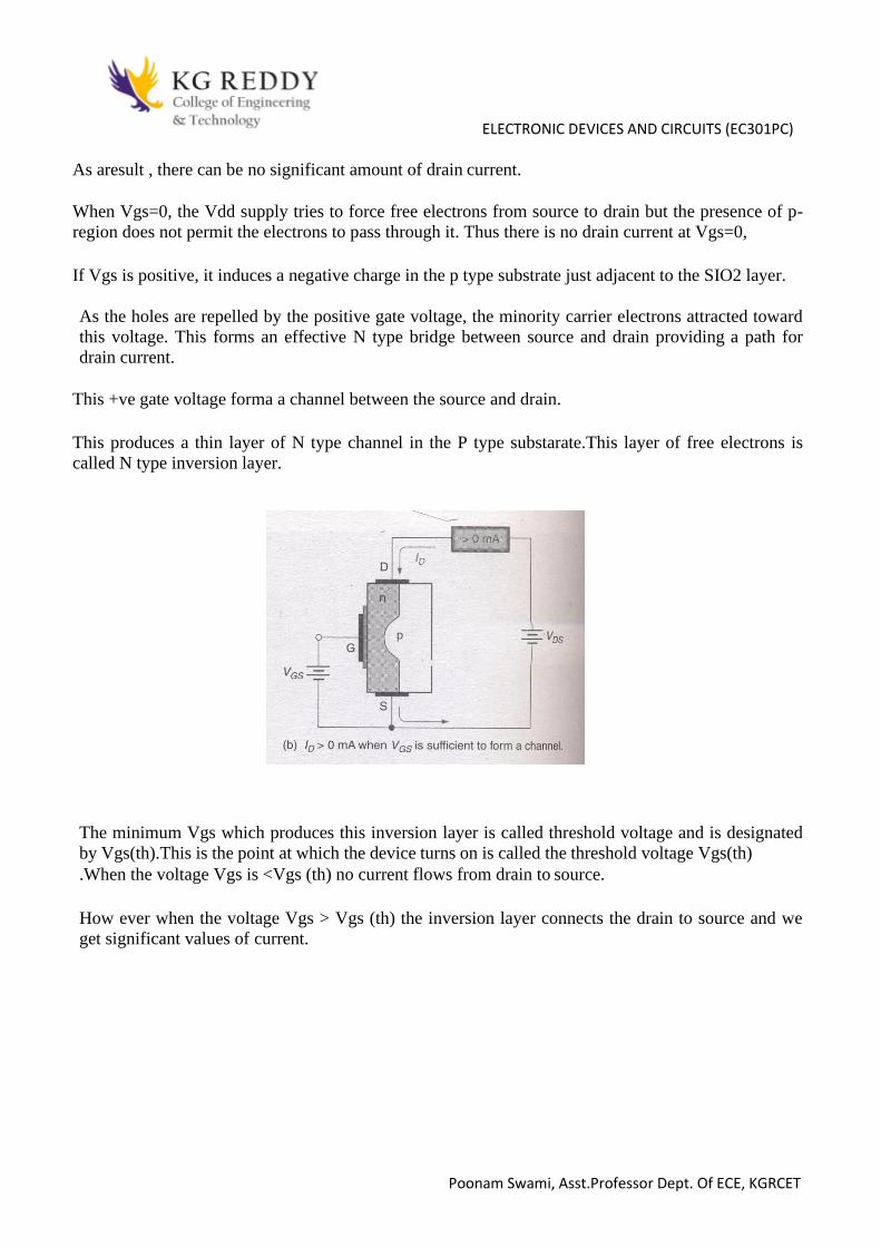
ELECTRONIC DEVICES AND CIRCUITS (EC301PC)
Poonam Swami, Asst.Professor Dept. Of ECE, KGRCET
As aresult , there can be no significant amount of drain current.
When Vgs=0, the Vdd supply tries to force free electrons from source to drain but the presence of p-
region does not permit the electrons to pass through it. Thus there is no drain current at Vgs=0,
If Vgs is positive, it induces a negative charge in the p type substrate just adjacent to the SIO2 layer.
As the holes are repelled by the positive gate voltage, the minority carrier electrons attracted toward
this voltage. This forms an effective N type bridge between source and drain providing a path for
drain current.
This +ve gate voltage forma a channel between the source and drain.
This produces a thin layer of N type channel in the P type substarate.This layer of free electrons is
called N type inversion layer.
The minimum Vgs which produces this inversion layer is called threshold voltage and is designated
by Vgs(th).This is the point at which the device turns on is called the threshold voltage Vgs(th)
.When the voltage Vgs is <Vgs (th) no current flows from drain to source.
How ever when the voltage Vgs > Vgs (th) the inversion layer connects the drain to source and we
get significant values of current.

ELECTRONIC DEVICES AND CIRCUITS (EC301PC)
Poonam Swami, Asst.Professor Dept. Of ECE, KGRCET
3. Draw and explain the common source amplifier.
Common Source (CS) Amplifier
Fig. 5.1 (a) CS Amplifier (b) Small-signal equivalent circuit
A simple Common Source amplifier is shown in Fig. 5.1(a) and associated small signal equivalent
circuit using voltage-source model of FET is shown in Fig. 5.1(b)
Voltage Gain
Source resistance (RS) is used to set the Q-Point but is bypassed by CS for mid-frequency operation.
From the small signal equivalent circuit ,the output voltage
VO = -RDµVgs(RD + rd)
Where Vgs = Vi , the input voltage, Hence, the voltage gain,
AV = VO / Vi = -RDµ(RD + rd)
Input Impedence
From Fig. 5.1(b) Input Impedence is Zi = RG
For voltage divider bias as in CE Amplifiers of BJT
RG = R1 ║ R2
Output Impedance
Output impedance is the impedance measured at the output terminals with the input voltage VI = 0
From the Fig. 5.1(b) when the input voltage Vi = 0, Vgs = 0 and hence
µ Vgs = 0
The equivalent circuit for calculating output impedence is given in Fig. 5.2. Output impedence Zo =
rd ║ RD
Normally rd will be far greater than RD . Hence Zo ≈ RD

ELECTRONIC DEVICES AND CIRCUITS (EC301PC)
Poonam Swami, Asst.Professor Dept. Of ECE, KGRCET
4. Draw and explain the common Drain amplifier
Common Drain Amplifier
A simple common drain amplifier is shown in Fig. 5.2(a) and associated small signal equivalent
circuit using the voltage source model of FET is shown in Fig. 5.2(b).Since voltage Vgd is more
easily determined than Vgs, the voltage source in the output circuit is expressed in terms of Vgs and
Thevenin’s theorem.
Fig. 5.2 (a)CD Amplifier (b)Small-signal equivalent circuit
Voltage Gain
The output voltage,
VO = RSµVgd / (µ + 1) RS + rd Where Vgd = Vi the input voltage. Hence, the voltage gain,
Av = VO / Vi = RSµ / (µ + 1) RS + rd
Input Impedence
From Fig. 5.2(b), Input Impedence Zi = RG
Output Impedence
From Fig. 5.2(b), Output impedence measured at the output terminals with input voltage Vi = 0 can
be calculated from the following equivalent circuit.

ELECTRONIC DEVICES AND CIRCUITS (EC301PC)
Poonam Swami, Asst.Professor Dept. Of ECE, KGRCET
As Vi = 0: Vgd = 0: µvgd / (µ + 1) = 0 Output Impedence
ZO = rd / (µ + 1) ║RS
When µ » 1
ZO = ( rd / µ) ║RS = (1/gm) ║RS
5. Establish a relation between the three JFET parameters, μ, rd and gm.
The electrical behavior of JFET may be described in terms of certain parameters. Such parameters
are obtained from the characteristic curves.
A C Drain resistance(rd):
It is also called dynamic drain resistance and is the a.c.resistance between the drain and source
terminal,when the JFET is operating in the pinch off or saturation region.It is given by the ratio of
small change in drain to source voltage ∆Vds to the corresponding change in drain current ∆Id for
a constant gate to source voltage Vgs.
Mathematically it is expressed as rd=∆Vds/ ∆Id where Vgs is held constant. TRANCE
CONDUCTANCE (gm):
It is also called forward transconductance. It is given by the ratio of small change in drain current
(∆Id) to the corresponding change in gate to source voltage (∆Vds)
Mathematically the transconductance can be written as gm=∆Id/∆Vds
AMPLIFICATION FACTOR (µ)
It is given by the ratio of small change in drain to source voltage (∆Vds) to the corresponding
change in gate to source voltage (∆Vgs)for a constant drain current (Id).
Thus µ=∆Vds/∆Vgs when Id held constant
The amplification factor µ may be expressed as a product of transconductance (gm)and ac drain
resistance (rd)
µ=∆Vds/∆Vgs

Electronic devices and circuits (EC301PC)
Poonam swami, Assist. Professor, Dept. of ECE, KGRCET
Multiple Choice Questions
1. Ideal maximum voltage for common drain amplifier is
A. 0
B. 1
C. 0.5
D. 2
2. If a certain JFET has a transconductance og 4mS and ha Ve external drain resistance of 1.5
Ω than ideal voltage gain will be
A. 4
B. 5
C. 6
D. 8
3. Input resistance of gate of amplifier is
A. zero
B. infinite
C. extremely low
D. extremely high
4. A FET circuit has a transconductance of 2500µS and drain resistance equals to 10k Ω than
voltage gain will be
A. 20
B. 25
C. 30
D. 35
5. voltage gain of common drain amplifier is always slightly less than
A. 0.5
B. 1
C. 1.5
D. 2

Electronic devices and circuits (EC301PC)
Poonam swami, Assist. Professor, Dept. of ECE, KGRCET
6. Drain of FET is analogues to BJT
A. collector
B. emitter
C. base
D. drain
7. When gate to source voltage of common source amplifier is at positive peak, drain to source
voltage will be
A. at positive peak
B. at negati Ve peak
C. infinite
D. zero
8. Common drain amplifier doesn't contain
A. source resistance
B. drain resistance
C. gate resistance
D. None of these
9. Input signal of common drain amplifier is applied to gate through
A. input resistor
B. coupling capacitor
C. output capacitor
D. transformer
10. Common source amplifier's source is connected to
A. drain
B. gate
C. ground
D. body

Electronic devices and circuits (EC301PC)
Poonam swami, Assist. Professor, Dept. of ECE, KGRCET
Fill in the blanks:
1. The gate-to-source voltage VGS of a(n) ________ must be larger than the threshold VGS(Th) for the
transistor to conduct.
2. ________ is the network-input impedance for a JFET fixed-bias configuration.
3. The ________ does not support Shockley's equation
4. The transconductance gm ________ as the Q-point moves from Vp to IDSS
5.The depletion MOSFET circuit has a ________ input impedance than a similar JFET
configuration.
6. The ________ controls the ________ of an FET.
7. Transconductance is the ratio of changes in ________.
8.________ is an undefined quantity in a JFET.
9. …………. has the lowest noise-level
10. The pinch-off voltage of a JFET is about ……….
Solutions
MCQ’s Fill in the blanks
1. B 1. E-type MOSFET
1. C RG
3.D E-type MOSFET
4. B Increases
5.B Much higher
6.A VGS, ID
7.B ID to VGS
8.B Ai
9.B JFET
10.C 5 V

Electronic devices and circuits (EC301PC)
Poonam swami, Assist. Professor, Dept. of ECE, KGRCET
17. CO, PO Mapping
PO1 PO2 PO3 PO4 PO5 PO6 PO7 PO8 PO9 PO10 PO11 PO12
CO1
H
M
CO2 H M
CO3 H M
CO4 H
L
CO5 L H M
CO6 L H M
Legends:
L: Low level
M: Medium level
H: High level

Electronic devices and circuits (EC301PC)
Poonam swami, Assist. Professor, Dept. of ECE, KGRCET
18. beyond syllabus Topics with material
1. Feedback amplifiers
An amplifier circuit simply increases the signal strength. But while amplifying, it just increases the
strength of its input signal whether it contains information or some noise along with information.
This noise or some disturbance is introduced in the amplifiers because of their strong tendency to
introduce hum due to sudden temperature changes or stray electric and magnetic fields. Therefore,
every high gain amplifier tends to give noise along with signal in its output, which is very
undesirable.
The noise level in the amplifier circuits can be considerably reduced by using negative
feedback done by injecting a fraction of output in phase opposition to the input signal.
Principle of Feedback Amplifier
A feedback amplifier generally consists of two parts. They are the amplifierand the feedback
circuit. The feedback circuit usually consists of resistors. The concept of feedback amplifier can
be understood from the following figure.
From the above figure, the gain of the amplifier is represented as A. the gain of the amplifier is the
ratio of output voltage Vo to the input voltage Vi. the feedback network extracts a voltage Vf = β
Vo from the output Vo of the amplifier.

Electronic devices and circuits (EC301PC)
Poonam swami, Assist. Professor, Dept. of ECE, KGRCET
This voltage is added for positive feedback and subtracted for negative feedback, from the signal
voltage Vs. Now,
Vi=Vs+Vf=Vs+βVoVi=Vs+Vf=Vs+βVo
Vi=Vs−Vf=Vs−βVoVi=Vs−Vf=Vs−βVo
The quantity β = Vf/Vo is called as feedback ratio or feedback fraction.
Let us consider the case of negative feedback. The output Vo must be equal to the input voltage
(Vs - βVo) multiplied by the gain A of the amplifier.
Hence,
(Vs−βVo)A=Vo(Vs−βVo)A=Vo
Or
AVs−AβVo=VoAVs−AβVo=Vo
Or
AVs=Vo(1+Aβ)AVs=Vo(1+Aβ)
Therefore,
VoVs=A1+AβVoVs=A1+Aβ
Let Af be the overall gain (gain with the feedback) of the amplifier. This is defined as the ratio of
output voltage Vo to the applied signal voltage Vs, i.e.,
Af=OutputvoltageInputsignalvoltage=VoVsAf=OutputvoltageInputsignalvoltage=VoVs
So, from the above two equations, we can understand that,
The equation of gain of the feedback amplifier, with negative feedback is given by
Af=A1+AβAf=A1+Aβ
The equation of gain of the feedback amplifier, with positive feedback is given by
Af=A1−AβAf=A1−Aβ
These are the standard equations to calculate the gain of feedback amplifiers.

Electronic devices and circuits (EC301PC)
Poonam swami, Assist. Professor, Dept. of ECE, KGRCET
Types of Feedbacks
The process of injecting a fraction of output energy of some device back to the input is known
as Feedback. It has been found that feedback is very useful in reducing noise and making the
amplifier operation stable.
Depending upon whether the feedback signal aids or opposes the input signal, there are two types
of feedbacks used.
Positive Feedback
The feedback in which the feedback energy i.e., either voltage or current is in phase with the input
signal and thus aids it is called as Positive feedback.
Both the input signal and feedback signal introduces a phase shift of 180o thus making a
360o resultant phase shift around the loop, to be finally in phase with the input signal.
Though the positive feedback increases the gain of the amplifier, it has the disadvantages such as
• Increasing distortion
• Instability
It is because of these disadvantages the positive feedback is not recommended for the amplifiers. If
the positive feedback is sufficiently large, it leads to oscillations, by which oscillator circuits are
formed. This concept will be discussed in OSCILLATORS tutorial.
Negative Feedback
The feedback in which the feedback energy i.e., either voltage or current is out of phase with the
input and thus opposes it, is called as negative feedback.
In negative feedback, the amplifier introduces a phase shift of 180o into the circuit while the
feedback network is so designed that it produces no phase shift or zero phase shift. Thus the
resultant feedback voltage Vf is 180o out of phase with the input signal Vin.
Though the gain of negative feedback amplifier is reduced, there are many advantages of negative
feedback such as
• Stability of gain is improved
• Reduction in distortion
• Reduction in noise

Electronic devices and circuits (EC301PC)
Poonam swami, Assist. Professor, Dept. of ECE, KGRCET
• Increase in input impedance
• Decrease in output impedance
• Increase in the range of uniform application
It is because of these advantages negative feedback is frequently employed in amplifiers.

Electronic devices and circuits (EC301PC)
Poonam swami, Assist. Professor, Dept. of ECE, KGRCET
2. Oscillators
An oscillator is a circuit which produces a continuous, repeated, alternating waveform without any
input. Oscillators basically convert unidirectional current flow from a DC source into an alternating
waveform which is of the desired frequency, as decided by its circuit components. The basic
principle behind the working of oscillators can be understood by analyzing the behavior of an LC
tank circuit shown by Figure 1, which employs an inductor L and a completely pre-charged
capacitor C as its components. Here, at first, the capacitor starts to discharge via the inductor, which
results in the conversion of its electrical energy into the electromagnetic field, which can be stored
in the inductor. Once the capacitor discharges completely, there will be no current flow in the
circuit.
However, by then, the stored electromagnetic field would have generated a back-emf which results
in the flow of current through the circuit in the same direction as that of before. This current flow
through the circuit continues until the electromagnetic field collapses which result in the back-
conversion of electromagnetic energy into electrical form, causing the cycle to repeat. However,
now the capacitor would have charged with the opposite polarity, due to which one gets an
oscillating waveform as the output.
However, the oscillations which arise due to the inter-conversion between the two energy-forms
cannot continue forever as they would be subjected to the effect of energy loss due to the resistance
of the circuit. As a result, the amplitude of these oscillations decreases steadily to become zero,
which makes them damped in nature. This indicates that in order to obtain the oscillations which
are continuous and of constant amplitude, one needs to compensate for the energy lost.
Nevertheless, it is to be noted that the energy supplied should be precisely controlled and must be
equal to that of the energy lost in order to obtain the oscillations with constant amplitude.
This is because, if the energy supplied is more than the energy lost, then the amplitude of the
oscillations will increase (Figure 2a) leading to a distorted output; while if the energy supplied is
less than the energy lost, then the amplitude of the oscillations will decrease (Figure 2b) leading to
unsustainable oscillations.

Electronic devices and circuits (EC301PC)
Poonam swami, Assist. Professor, Dept. of ECE, KGRCET
Practically, the oscillators are nothing but the amplifier circuits which are provided with a positive
or regenerative feedback wherein a part of the output signal is fed back to the input (Figure 3). Here
the amplifier consists of an amplifying active element which can be a transistor or an Op-Amp and
the back-fed in-phase signal is held responsible to keep-up (sustain) the oscillations by making-up
for the losses in the circuit.
Once the power supply is switched ON, the oscillations will be initiated in the system due to the
electronic noise present in it. This noise signal travels around the loop, gets amplified and
converges to a single frequency sine wave very quickly. The expression for the closed loop gain of
the oscillator shown in Figure 3 is given as
Where A is the voltage gain of the amplifier and β is the gain of the feedback network. Here, if Aβ
> 1, then the oscillations will increase in amplitude (Figure 2a); while if Aβ < 1, then the
oscillations will be damped (Figure 2b). On the other hand, Aβ = 1 leads to the oscillations which

Electronic devices and circuits (EC301PC)
Poonam swami, Assist. Professor, Dept. of ECE, KGRCET
are of constant amplitude (Figure 2c). In other words, this indicates that if the feedback loop gain is
small, then the oscillation dies-out, while if the gain of the feedback loop is large, then the output
will be distorted; and only if the gain of feedback is unity, then the oscillations will be of constant
amplitude leading to self-sustained oscillatory circuit. Oscillators are primarily of two categories
viz., Linear or Harmonic Oscillators and Relaxation Oscillators. In harmonic oscillators, the energy
flow is always from the active components to the passive components and the frequency of
oscillations is decided by the feedback path. However, in the case of relaxation oscillators, the
energy is exchanged between the active and the passive components and the frequency of
oscillations is determined by the charging and discharging time-constants involved in the process.
Further, harmonic oscillators produce low-distorted sine-wave outputs while the relaxation
oscillators generate non-sinusoidal (saw-tooth, triangular or square) wave-forms.
Oscillators can be classified into various types depending on the parameter considered viz.,
Classification Based on the Feedback Mechanism: Positive Feedback Oscillators and Negative
Feedback Oscillators.
Classification Based on the Shape of the Output Waveform: Sine Wave Oscillators, Square or
Rectangular Wave oscillators, Sweep Oscillators (which produce saw-tooth output waveform), etc.
Classification Based on the Frequency of the Output Signal: Low Frequency Oscillators, Audio
Oscillators (whose output frequency is of audio range), Radio Frequency Oscillators, High
Frequency Oscillators, Very High Frequency Oscillators, Ultra High Frequency Oscillators, etc.
Classification Based on the type of the Frequency Control Used: RC Oscillators, LC
Oscillators, Crystal Oscillators (which use a quartz crystal to result in a frequency stabilized output
waveform), etc.
Classification Based on the Nature of the Frequency of Output Waveform: Fixed Frequency
Oscillators and Variable or Tunable Frequency Oscillators.
Few examples of oscillators are Armstrong Oscillators, Hartley Oscillators, Colpitts Oscillators,
Clapp Oscillators, Cross-Coupled Oscillators, Dynatron Oscillators, Meissner Oscillators, Opto-
Electronic Oscillators, Pierce Oscillators, Phase-Shift Oscillators, Robinson Oscillators, Tri-tet
Oscillators, Wein-Bridge Oscillators, Pearson-Anson Oscillators, Ring Oscillators, Delay-Line
Oscillators, Royer Oscillators, Electron Coupled Oscillators and Multi-Wave Oscillators.
Oscillators are portable and cheap due to which they are extensively used in quartz watches, radio
receivers, computers, metal detectors, stun guns, inverters, ultrasonic and radio frequency
applications.


![misscollege.edu.in · MADURAI INSTITUTE OF SOCIAL SCIENCES (AUTONOMOUS) COURSE OUTCOME FOR COMMERCE [BCOM CA] YEAR I SEMESTER I COURSE CODE COURSE COURSE OUTCOMES 18BCOMCL11 VANIKA](https://img.pdfslide.us/doc/110x75/5eac03380b97fc65a27eb5db/madurai-institute-of-social-sciences-autonomous-course-outcome-for-commerce-bcom.jpg)