Embed Size (px)
Citation preview
3-A, 3.3/5-V INPUT, ADJUSTABLE SWITCHING REGULATOR
1FEATURES
APPLICATIONS
DESCRIPTION
1
5
2
3
4
6
+
PTH04000W(Top View)
Track
GND
R #
1%, 0.1 W(Required)
SETInhibit
C
47 F(Required)
I
µ
*C
47 F(Optional)
O*µ
VI
VO
GND
STANDARD APPLICATION
* See the Application Information section for capacitor recommendations.
# See the Application Information section for R values.SET
PTH04000W
SLTS247B–JUNE 2005–REVISED OCTOBER 2007www.ti.com
WITH AUTO-TRACK™ SEQUENCING• Point-of-Load Alliance (POLA™) Compatible
2• Up to 3-A Output Current at 85°C • Surface Mount Package• 3.3-V / 5-V Input Voltage • Safety Agency Approvals:
- UL/IEC/CSA-22.2 60950-1• Wide-Output Voltage Adjust(0.9 V to 3.6 V)
• Efficiencies Up To 94%• Telecommunications, Instrumentation,• On/Off Inhibit and General-Purpose Circuits
• Undervoltage Lockout (UVLO)• Output Overcurrent Protection
(Nonlatching, Auto-Reset)• Overtemperature Protection• Ambient Temperature Range: –40°C to 85°C
The PTH04000W is a highly integrated, low-cost switching regulator module that delivers up to 3 A of outputcurrent. Occupying a small PCB area, the PTH04000W provides output current at a high efficiency and withminimal power dissipation, thereby eliminating the need for a heat sink. Their small size (0.75 inch × 0.5 inch),high efficiency, and low cost makes these modules practical for a variety of applications.
The input voltage range of the PTH04000W is from 3 V to 5.5 V, allowing operation from either a 3.3-V or 5-Vinput bus. Using state-of-the-art switched-mode power-conversion technology, the PTH04000W can step down tovoltages as low as 0.9 V from a 5-V input bus, with typically less than 1 W of power dissipation. The outputvoltage can be adjusted to any voltage over the range, 0.9 V to 3.6 V, using a single external resistor. This seriesincludes Auto-Track™ sequencing. This feature simplifies the task of supply voltage sequencing in a powersystem by enabling modules to track each other, or any external voltage, during power up and power down.Other operating features include an undervoltage lockout (UVLO), on/off inhibit, output overcurrent protection,and overtemperature protection. Target applications include telecommunications, test and measurementapplications, and high-end consumer products. The modules are available in both through-hole andsurface-mount package options, including tape and reel. The PTH04000W is also compatible with TI's roadmapfor RoHS and lead-free compliance.
1
Please be aware that an important notice concerning availability, standard warranty, and use in critical applications ofTexas Instruments semiconductor products and disclaimers thereto appears at the end of this data sheet.
2POLA, Auto-Track, TMS320 are trademarks of Texas Instruments.
PRODUCTION DATA information is current as of publication date. Copyright © 2005–2007, Texas Instruments IncorporatedProducts conform to specifications per the terms of the TexasInstruments standard warranty. Production processing does notnecessarily include testing of all parameters.
www.ti.com
ABSOLUTE MAXIMUM RATINGS
RECOMMENDED OPERATING CONDITIONS
PACKAGE SPECIFICATIONS
PTH04000W
SLTS247B–JUNE 2005–REVISED OCTOBER 2007
These devices have limited built-in ESD protection. The leads should be shorted together or the device placed in conductive foamduring storage or handling to prevent electrostatic damage to the MOS gates.
ORDERING INFORMATIONFor the most current package and ordering information, see the Package Option Addendum at the end of this datasheet, or seethe TI website at www.ti.com.
over operating free-air temperature range unless otherwise noted (1)
PTH04000W UNITTA Operating free-air temperature Over VI range -40 to 85 °C
Lead temperature (H suffix) 5 seconds 260Solder reflow temperature (S suffix) Surface temperature of module body or pins 235 °CSolder reflow temperature (Z suffix) (2) Surface temperature of module body or pins 260 (2)
Tstg Storage temperature -55 to 125 °C
(1) Stresses beyond those listed under absolute maximum ratings may cause permanent damage to the device. These are stress ratingsonly, and functional operation of the device at these or any other conditions beyond those indicated under recommended operatingconditions is not implied. Exposure to absolute-maximum-rated conditions for extended periods may affect device reliability.
(2) Moisture Sensitivity Level (MSL) Rating Level-3-260C-168HR
MIN MAX UNITVI Input voltage 3 5.5 VTA Operating free-air temperature -40 85 °C
PTH04000Wx (Suffix AH, AS and AZ)Weight 1.5 grams
Flammability Meets UL 94 V-OMechanical shock Per Mil-STD-883D, Method 2002.3, 1 msec, sine, mounted 500 G (1)
Mechanical vibration Mil-STD-883D, Method 2007.2, 20-2000 Hz 20 G (1)
(1) Qualification limit.
2 Submit Documentation Feedback Copyright © 2005–2007, Texas Instruments Incorporated
Product Folder Link(s): PTH04000W
www.ti.com
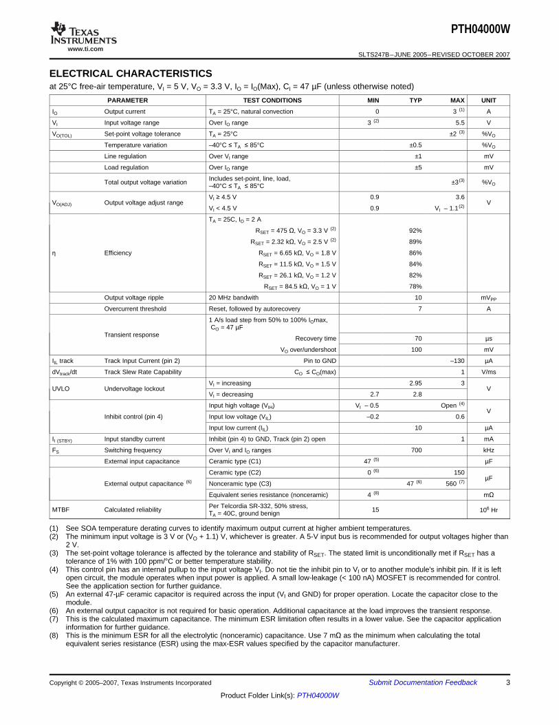
ELECTRICAL CHARACTERISTICS
PTH04000W
SLTS247B–JUNE 2005–REVISED OCTOBER 2007
at 25°C free-air temperature, VI = 5 V, VO = 3.3 V, IO = IO(Max), CI = 47 µF (unless otherwise noted)PARAMETER TEST CONDITIONS MIN TYP MAX UNIT
IO Output current TA = 25°C, natural convection 0 3 (1) A
VI Input voltage range Over IO range 3 (2) 5.5 V
VO(TOL) Set-point voltage tolerance TA = 25°C ±2 (3) %VO
Temperature variation –40°C ≤ TA ≤ 85°C ±0.5 %VO
Line regulation Over VI range ±1 mV
Load regulation Over IO range ±5 mV
Includes set-point, line, load,Total output voltage variation ±3 (3) %VO–40°C ≤ TA ≤ 85°C
VI ≥ 4.5 V 0.9 3.6VO(ADJ) Output voltage adjust range V
VI < 4.5 V 0.9 VI – 1.1 (2)
TA = 25C, IO = 2 A
RSET = 475 Ω, VO = 3.3 V (2) 92%
RSET = 2.32 kΩ, VO = 2.5 V (2) 89%
η Efficiency RSET = 6.65 kΩ, VO = 1.8 V 86%
RSET = 11.5 kΩ, VO = 1.5 V 84%
RSET = 26.1 kΩ, VO = 1.2 V 82%
RSET = 84.5 kΩ, VO = 1 V 78%
Output voltage ripple 20 MHz bandwith 10 mVPP
Overcurrent threshold Reset, followed by autorecovery 7 A
1 A/s load step from 50% to 100% IOmax,CO = 47 µF
Transient response Recovery time 70 µs
VO over/undershoot 100 mV
IIL track Track Input Current (pin 2) Pin to GND –130 µA
dVtrack/dt Track Slew Rate Capability CO ≤ CO(max) 1 V/ms
VI = increasing 2.95 3UVLO Undervoltage lockout V
VI = decreasing 2.7 2.8
Input high voltage (VIH) VI – 0.5 Open (4)
VInhibit control (pin 4) Input low voltage (VIL) –0.2 0.6
Input low current (IIL) 10 µA
II (STBY) Input standby current Inhibit (pin 4) to GND, Track (pin 2) open 1 mA
FS Switching frequency Over VI and IO ranges 700 kHz
External input capacitance Ceramic type (C1) 47 (5) µF
Ceramic type (C2) 0 (6) 150µF
External output capacitance (6) Nonceramic type (C3) 47 (6) 560 (7)
Equivalent series resistance (nonceramic) 4 (8) mΩ
Per Telcordia SR-332, 50% stress,MTBF Calculated reliability 15 106 HrTA = 40C, ground benign
(1) See SOA temperature derating curves to identify maximum output current at higher ambient temperatures.(2) The minimum input voltage is 3 V or (VO + 1.1) V, whichever is greater. A 5-V input bus is recommended for output voltages higher than
2 V.(3) The set-point voltage tolerance is affected by the tolerance and stability of RSET. The stated limit is unconditionally met if RSET has a
tolerance of 1% with 100 ppm/°C or better temperature stability.(4) This control pin has an internal pullup to the input voltage VI. Do not tie the inhibit pin to VI or to another module's inhibit pin. If it is left
open circuit, the module operates when input power is applied. A small low-leakage (< 100 nA) MOSFET is recommended for control.See the application section for further guidance.
(5) An external 47-µF ceramic capacitor is required across the input (VI and GND) for proper operation. Locate the capacitor close to themodule.
(6) An external output capacitor is not required for basic operation. Additional capacitance at the load improves the transient response.(7) This is the calculated maximum capacitance. The minimum ESR limitation often results in a lower value. See the capacitor application
information for further guidance.(8) This is the minimum ESR for all the electrolytic (nonceramic) capacitance. Use 7 mΩ as the minimum when calculating the total
equivalent series resistance (ESR) using the max-ESR values specified by the capacitor manufacturer.
Copyright © 2005–2007, Texas Instruments Incorporated Submit Documentation Feedback 3
Product Folder Link(s): PTH04000W
www.ti.com
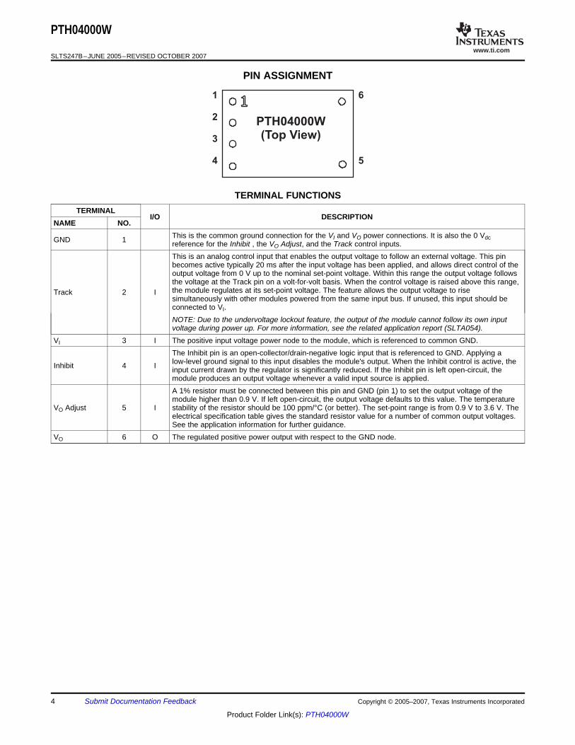
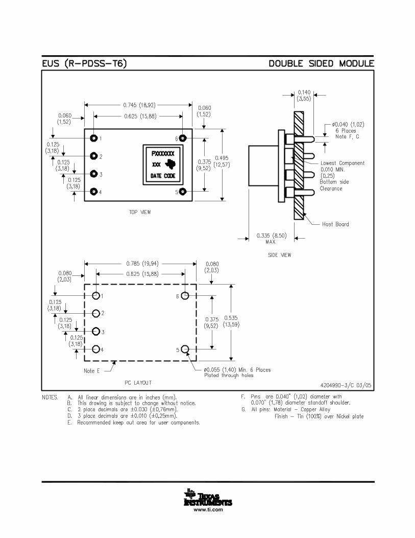
PIN ASSIGNMENT
PTH04000W(Top View)
1
5
2
3
4
6
PTH04000W
SLTS247B–JUNE 2005–REVISED OCTOBER 2007
TERMINAL FUNCTIONSTERMINAL
I/O DESCRIPTIONNAME NO.
This is the common ground connection for the VI and VO power connections. It is also the 0 VdcGND 1 reference for the Inhibit , the VO Adjust, and the Track control inputs.This is an analog control input that enables the output voltage to follow an external voltage. This pinbecomes active typically 20 ms after the input voltage has been applied, and allows direct control of theoutput voltage from 0 V up to the nominal set-point voltage. Within this range the output voltage followsthe voltage at the Track pin on a volt-for-volt basis. When the control voltage is raised above this range,the module regulates at its set-point voltage. The feature allows the output voltage to riseTrack 2 Isimultaneously with other modules powered from the same input bus. If unused, this input should beconnected to VI.NOTE: Due to the undervoltage lockout feature, the output of the module cannot follow its own inputvoltage during power up. For more information, see the related application report (SLTA054).
VI 3 I The positive input voltage power node to the module, which is referenced to common GND.The Inhibit pin is an open-collector/drain-negative logic input that is referenced to GND. Applying alow-level ground signal to this input disables the module's output. When the Inhibit control is active, theInhibit 4 I input current drawn by the regulator is significantly reduced. If the Inhibit pin is left open-circuit, themodule produces an output voltage whenever a valid input source is applied.A 1% resistor must be connected between this pin and GND (pin 1) to set the output voltage of themodule higher than 0.9 V. If left open-circuit, the output voltage defaults to this value. The temperature
VO Adjust 5 I stability of the resistor should be 100 ppm/°C (or better). The set-point range is from 0.9 V to 3.6 V. Theelectrical specification table gives the standard resistor value for a number of common output voltages.See the application information for further guidance.
VO 6 O The regulated positive power output with respect to the GND node.
4 Submit Documentation Feedback Copyright © 2005–2007, Texas Instruments Incorporated
Product Folder Link(s): PTH04000W
www.ti.com
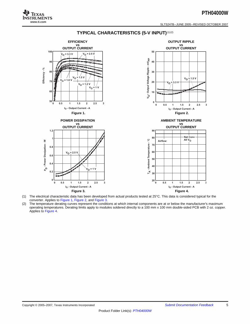
TYPICAL CHARACTERISTICS (5-V INPUT) (1) (2)
50
60
70
80
90
100
0 0.5 1 1.5 2 2.5 3
V = 3.3 VO
VO = 1.5 VVO = 1.8 V
VO = 1.2 V
VO = 1 V
Eff
icie
ncy -
%
IO - Output Current - A
V = 2.5 VO
0
10
20
30
40
50
0 0.5 1 1.5 2 2.5 3
VO
utp
ut
Vo
lta
ge
Rip
ple
- m
VO
PP
-
IO - Output Current - A
V = 3.3 VO
V = 1.5 VO
0
0.2
0.6
0.4
0.8
1
1.2
0 0.5 1 1.5 2 2.5 3
- P
ow
er
Dis
sip
ati
on
- W
PD
IO - Output Current - A
V = 2.5 VO
V = 1 VO
20
30
40
50
60
70
80
90
0 0.5 1 1.5 2 2.5 3
IO - Output Current - A
Airflow:
T-
Am
bie
nt
Tem
pera
ture
-C
Ao
Nat ConvAll VO
PTH04000W
SLTS247B–JUNE 2005–REVISED OCTOBER 2007
EFFICIENCY OUTPUT RIPPLEvs vs
OUTPUT CURRENT OUTPUT CURRENT
Figure 1. Figure 2.
POWER DISSIPATION AMBIENT TEMPERATUREvs vs
OUTPUT CURRENT OUTPUT CURRENT
Figure 3. Figure 4.(1) The electrical characteristic data has been developed from actual products tested at 25°C. This data is considered typical for the
converter. Applies to Figure 1, Figure 2, and Figure 3.(2) The temperature derating curves represent the conditions at which internal components are at or below the manufacturer's maximum
operating temperatures. Derating limits apply to modules soldered directly to a 100 mm x 100 mm double-sided PCB with 2 oz. copper.Applies to Figure 4.
Copyright © 2005–2007, Texas Instruments Incorporated Submit Documentation Feedback 5
Product Folder Link(s): PTH04000W
www.ti.com
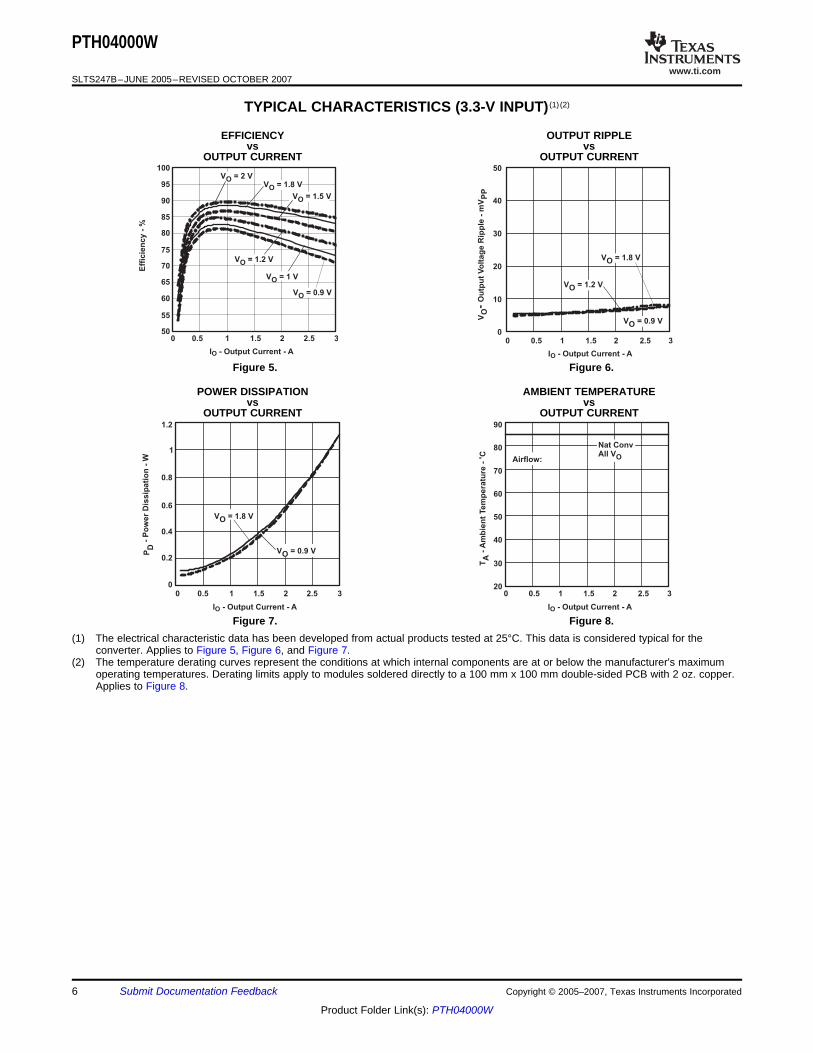
TYPICAL CHARACTERISTICS (3.3-V INPUT) (1) (2)
50
55
60
65
70
75
80
85
90
95
100
0 0.5 1 1.5 2 2.5 3
VO = 2 VVO = 1.8 V
VO = 1.5 V
VO = 1.2 V
VO = 1 V
VO = 0.9 V
Eff
icie
ncy -
%
IO - Output Current - A
0
10
20
30
40
50
0 0.5 1 1.5 2 2.5 3
VO
utp
ut
Vo
lta
ge
Rip
ple
- m
VO
PP
-
IO - Output Current - A
V = 1.2 VO
V = 0.9 VO
V = 1.8 VO
0
0.2
0.6
0.4
0.8
1
1.2
0 0.5 1 1.5 2 2.5 3
- P
ow
er
Dis
sip
ati
on
- W
PD
IO - Output Current - A
V = 1.8 VO
V = 0.9 VO
20
30
40
50
60
70
80
90
0 0.5 1 1.5 2 2.5 3
IO - Output Current - A
Airflow:
T-
Am
bie
nt
Tem
pera
ture
-C
Ao
Nat ConvAll VO
PTH04000W
SLTS247B–JUNE 2005–REVISED OCTOBER 2007
EFFICIENCY OUTPUT RIPPLEvs vs
OUTPUT CURRENT OUTPUT CURRENT
Figure 5. Figure 6.
POWER DISSIPATION AMBIENT TEMPERATUREvs vs
OUTPUT CURRENT OUTPUT CURRENT
Figure 7. Figure 8.(1) The electrical characteristic data has been developed from actual products tested at 25°C. This data is considered typical for the
converter. Applies to Figure 5, Figure 6, and Figure 7.(2) The temperature derating curves represent the conditions at which internal components are at or below the manufacturer's maximum
operating temperatures. Derating limits apply to modules soldered directly to a 100 mm x 100 mm double-sided PCB with 2 oz. copper.Applies to Figure 8.
6 Submit Documentation Feedback Copyright © 2005–2007, Texas Instruments Incorporated
Product Folder Link(s): PTH04000W
www.ti.com
APPLICATION INFORMATION
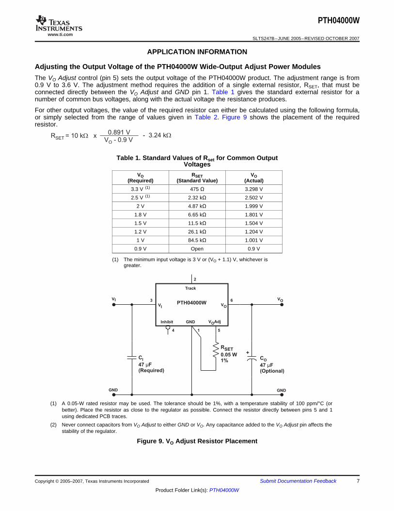
Adjusting the Output Voltage of the PTH04000W Wide-Output Adjust Power Modules
RSET = 10 k xW0.891 V
V - 0.9 VO
- 3.24 kW
VI
+
GNDGND
1 5
63
4
2
Track
VIVO
VO
GNDInhibit V AdjO
C
47 F(Required)
I
µ
PTH04000W
C
47 F(Optional)
O
µ
R
0.05 W1%
SET
PTH04000W
SLTS247B–JUNE 2005–REVISED OCTOBER 2007
The VO Adjust control (pin 5) sets the output voltage of the PTH04000W product. The adjustment range is from0.9 V to 3.6 V. The adjustment method requires the addition of a single external resistor, RSET, that must beconnected directly between the VO Adjust and GND pin 1. Table 1 gives the standard external resistor for anumber of common bus voltages, along with the actual voltage the resistance produces.
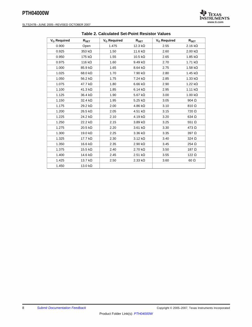
For other output voltages, the value of the required resistor can either be calculated using the following formula,or simply selected from the range of values given in Table 2. Figure 9 shows the placement of the requiredresistor.
Table 1. Standard Values of Rset for Common OutputVoltages
VO RSET VO(Required) (Standard Value) (Actual)
3.3 V (1) 475 Ω 3.298 V2.5 V (1) 2.32 kΩ 2.502 V
2 V 4.87 kΩ 1.999 V1.8 V 6.65 kΩ 1.801 V1.5 V 11.5 kΩ 1.504 V1.2 V 26.1 kΩ 1.204 V1 V 84.5 kΩ 1.001 V
0.9 V Open 0.9 V
(1) The minimum input voltage is 3 V or (VO + 1.1) V, whichever isgreater.
(1) A 0.05-W rated resistor may be used. The tolerance should be 1%, with a temperature stability of 100 ppm/°C (orbetter). Place the resistor as close to the regulator as possible. Connect the resistor directly between pins 5 and 1using dedicated PCB traces.
(2) Never connect capacitors from VO Adjust to either GND or VO. Any capacitance added to the VO Adjust pin affects thestability of the regulator.
Figure 9. VO Adjust Resistor Placement
Copyright © 2005–2007, Texas Instruments Incorporated Submit Documentation Feedback 7
Product Folder Link(s): PTH04000W
www.ti.com
PTH04000W
SLTS247B–JUNE 2005–REVISED OCTOBER 2007
Table 2. Calculated Set-Point Resistor ValuesVO Required RSET VO Required RSET VO Required RSET
0.900 Open 1.475 12.3 kΩ 2.55 2.16 kΩ0.925 353 kΩ 1.50 11.6 kΩ 2.60 2.00 kΩ0.950 175 kΩ 1.55 10.5 kΩ 2.65 1.85 kΩ0.975 116 kΩ 1.60 9.49 kΩ 2.70 1.71 kΩ1.000 85.9 kΩ 1.65 8.64 kΩ 2.75 1.58 kΩ1.025 68.0 kΩ 1.70 7.90 kΩ 2.80 1.45 kΩ1.050 56.2 kΩ 1.75 7.24 kΩ 2.85 1.33 kΩ1.075 47.7 kΩ 1.80 6.66 kΩ 2.90 1.22 kΩ1.100 41.3 kΩ 1.85 6.14 kΩ 2.95 1.11 kΩ1.125 36.4 kΩ 1.90 5.67 kΩ 3.00 1.00 kΩ1.150 32.4 kΩ 1.95 5.25 kΩ 3.05 904 Ω1.175 29.2 kΩ 2.00 4.86 kΩ 3.10 810 Ω1.200 26.5 kΩ 2.05 4.51 kΩ 3.15 720 Ω1.225 24.2 kΩ 2.10 4.19 kΩ 3.20 634 Ω1.250 22.2 kΩ 2.15 3.89 kΩ 3.25 551 Ω1.275 20.5 kΩ 2.20 3.61 kΩ 3.30 473 Ω1.300 19.0 kΩ 2.25 3.36 kΩ 3.35 397 Ω1.325 17.7 kΩ 2.30 3.12 kΩ 3.40 324 Ω1.350 16.6 kΩ 2.35 2.90 kΩ 3.45 254 Ω1.375 15.5 kΩ 2.40 2.70 kΩ 3.50 187 Ω1.400 14.6 kΩ 2.45 2.51 kΩ 3.55 122 Ω1.425 13.7 kΩ 2.50 2.33 kΩ 3.60 60 Ω1.450 13.0 kΩ
8 Submit Documentation Feedback Copyright © 2005–2007, Texas Instruments Incorporated
Product Folder Link(s): PTH04000W
www.ti.com
CAPACITOR RECOMMENDATIONS for the PTH04000W WIDE-OUTPUT
Input Capacitor
Output Capacitors (Optional)
Ceramic Capacitors
Tantalum Capacitors
Capacitor Table
PTH04000W
SLTS247B–JUNE 2005–REVISED OCTOBER 2007
ADJUST POWER MODULES
The minimum required input capacitor(s) is 47-µF of ceramic capacitance, in either an X5R or X7R temperaturetolerance. The ceramic capacitors should be located within 0.5 inch (1,27 cm) of the regulator's input pins.Electrolytic capacitors can also be used at the input, but only in addition to the required ceramic capacitance.The minimum ripple current rating for nonceramic capacitors should be at least 200 mA rms. The ripple currentrating of electrolytic capacitors is a major consideration when they are used at the input.
When specifying regular tantalum capacitors for use at the input, a minimum voltage rating of 2 × (maximum dcvoltage + ac ripple) is highly recommended. This is standard practice to ensure reliability. Polymer-tantalumcapacitors are not affected by this requirement.
For improved ripple reduction on the input bus, additional ceramic capacitors can be used to complement theminimum requirement.
For applications with load transients (sudden changes in load current), the regulator response benefits fromadditional external output capacitance. The recommended output capacitance of 47 µF allows the module tomeet its transient response specification. A high-quality computer-grade electrolytic capacitor should beadequate.
Electrolytic capacitors should be located close to the load circuit. These capacitors provide decoupling over thefrequency range, 2 kHz to 150 kHz. Aluminum electrolytic capacitors are suitable for ambient temperaturesabove 0°C. For operation below 0°C, tantalum or OS-CON type capacitors are recommended. When using oneor more nonceramic capacitors, the calculated equivalent ESR should be no lower than 4 mΩ (7 mΩ using themanufacturer's maximum ESR for a single capacitor). A list of preferred low-ESR type capacitors are identified inTable 3.
Above 150 kHz the performance of aluminum electrolytic capacitors becomes less effective. To further improvethe reflected input ripple current, or the output transient response, multilayer ceramic capacitors must be added.Ceramic capacitors have low ESR and their resonant frequency is higher than the bandwidth of the regulator.When placed at the output, their combined ESR is not critical as long as the total value of ceramic capacitancedoes not exceed 150 µF. Also, to prevent the formation of local resonances, do not exceed the maximumnumber of capacitors specified in the capacitor table.
Additional tantalum type capacitors can be used at both the input and output, and are recommended forapplications where the ambient operating temperature can be less than 0°C. The AVX TPS, Sprague593D/594/595, and Kemet T495/T510/T520 capacitors series are suggested over many other tantalum types dueto their rated surge, power dissipation, and ripple current capability. As a caution, many general-purposetantalum capacitors have considerably higher ESR and lower ripple current capability. These capacitors are alsoless reliable as they have lower power dissipation capability and surge current ratings. Tantalum capacitors thatdo not have a stated ESR or surge current rating are not recommended for power applications. When specifyingOS-CON and polymer-tantalum capacitors for the output, the minimum ESR limit is encountered well before themaximum capacitance value is reached.
The capacitor table, Table 3, identifies the characteristics of capacitors from a number of vendors withacceptable ESR and ripple current (rms) ratings. The recommended number of capacitors required at both theinput and output buses is identified for each capacitor type. This is not an extensive capacitor list. Capacitorsfrom other vendors are available with comparable specifications. Those listed are for guidance. The rms ratingand ESR (at 100 kHz) are critical parameters necessary to insure both optimum regulator performance and longcapacitor life.
Copyright © 2005–2007, Texas Instruments Incorporated Submit Documentation Feedback 9
Product Folder Link(s): PTH04000W
www.ti.com
Designing for Load Transients
PTH04000W
SLTS247B–JUNE 2005–REVISED OCTOBER 2007
The transient response of the dc/dc converter has been characterized using a load transient with a di/dt of 1 A/s.The typical voltage deviation for this load transient is given in the data sheet specification table using the optionalvalue of output capacitance. As the di/dt of a transient is increased, the response of a converter's regulationcircuit ultimately depends on its output capacitor decoupling network. This is an inherent limitation with any dc/dcconverter once the speed of the transient exceeds its bandwidth capability. If the target application specifies ahigher di/dt or lower voltage deviation, the requirement can only be met with additional output capacitordecoupling. In these cases, special attention must be paid to the type, value, and ESR of the capacitors selected.
If the transient performance requirements exceed those specified in the data sheet, the selection of outputcapacitors becomes more important. Review the minimum ESR in the characteristic data sheet for details on thecapacitance maximum.
Table 3. Recommended Input/Output Capacitors (1)
CAPACITOR CHARACTERISTICS QUANTITY
85CCAPACITOR VENDOR/ EQUIVALENT VENDORMAXIMUM PHYSICALCOMPONENT WORKING VALUE SERIES INPUT OUTPUT NUMBERRIPPLE SIZESERIES VOLTAGE (F) RESISTANCE BUS (2) BUSCURRENT (mm)(ESR) (Irms)
Panasonic WA (SMT) 10 V 120 0.035 Ω 2800 mA 8 × 6,9 1 ≤ 4 (2) EEFWA1A121P (3)
FC (SMT) 25 V 47 0.400 Ω 230 mA 8 × 6,2 1 1 (2) EEVFC1E470P (3)
6.3 V 47 0.018 Ω 2500 mA 7,3 ×4,3 1 ≤ 2 EEFCD0J470RPanasonic SL SP-cap(SMT) 6.3 V 56 0.009 Ω 3000 mA 7,3 × 4,3 1 ≤ 1 EEFSL0J560R
United Chemi-con PXA (SMT) 10 V 47 0.031 Ω 2250 mA 6,3 × 5,7 1 1 PXA10VC470MF60TPFS 10 V 100 0.040 Ω 2100 mA 6,3 × 9,8 1 ≤ 3 10FS100MLXZ 16 V 100 0.250 Ω 290 mA 6,3 × 11,5 1 1 LXZ16VB101M6X11LLMVZ (SMT) 16 V 100 0.440 Ω 230 mA 6,3 × 5,7 1 1 MVZ16VC101MF60TP
Nichicon UWG (SMT) 16 V 100 0.400 Ω 230 mA 8 × 6,2 1 1 UWG1C101MCR1GSF559(Tantalum) 10 V 100 0.055 Ω 2000 mA 7,7 × 4,3 1 ≤ 3 F551A107MNPM 10 V 100 0.550 Ω 210 mA 6 × 11 1 1 UPM1A101MEH
Sanyo Os-con\ POS-Cap SVP 10 V 68 0.025 Ω 2400 mA 7,3 × 4,3 1 ≤ 3 10TPE68M(SMT) 6.3 V 47 0.074 Ω 1110 mA 5 × 6 1 ≤ 3 6SVP47MSP 10 V 56 0.045 Ω 1710 mA 6,3 × 5 1 ≤ 3 10SP56M
10 V 47 0.100 Ω 1100 mA 7,3L × 4,3W 1 ≤ 3 TPSD476M010R0100AVX Tantalum TPS (SMD) 10 V 47 0.060 Ω > 412 mA × 4,1H 1 ≤ 53 TPSB476M010R0500
Kemet T520 (SMD) 10 V 68 0.060 Ω >1200 mA 7,3L × 5,7W 1 ≤ 3 T520V686M010ASE060AO-CAP 6.3 V 47 0.028 Ω >1100 mA × 4H 1 ≤ 3 A700V476M006AT
Vishay/Sprague 594D/595D 10 V 68 0.100 Ω >1000 mA 7,3L × 6W × 1 ≤ 3 594D686X0010C2T(SMD) 10 V 68 0.240 Ω 680 mA 4,1H 1 ≤ 3 595D686X0010C2T
94SL 16 V 47 0.070 Ω 1550 mA 8 × 5 1 ≤ 3 94SL476X0016EBP
7,5L × 4,0WTDK Ceramic X5R (Leaded) 10 V 47 0.005 Ω >1400 mA ≥ 1 ≤ 2 FK22X5R1A476M× 8,0H
TDK Ceramic X5R 6.3 V 22 0.002 Ω >1400 mA ≥ 2 (4) ≤ 3 C3225X5R0J226KT/MT1210 caseMurata Ceramic X5R 6.3 V 22 0.002 Ω >1000 mA ≥ 2 (4) ≤ 3 GRM32ER61J223M3225 mmKemet 6.3 V 22 0.002 Ω >1000 mA ≥ 2 (4) ≤ 3 C1210C226K9PAC
TDK Ceramic X5R 6.3 V 47 0.002 Ω >1400 mA ≥ 1 ≤ 2 C3225X5R0J476KT/MT1210 caseMurata Ceramic X5R 6.3 V 47 0.002 Ω >1000 mA ≥ 1 ≤ 2 GRM32ER60J476M/6.33225 mmKemet 6.3 V 47 0.002 Ω >1000 mA ≥ 1 ≤ 2 C1210C476K9PAC
(1) Check with capacitor manufacturers for availability and lead-free status.(2) A ceramic capacitor is required on the input. An electrolytic capacitor can be added to the output for improved transient response.(3) An optional through-hole capacitor available.(4) A total capacitance of 44 µF is an acceptable replacement for a single 47-µF capacitor.
10 Submit Documentation Feedback Copyright © 2005–2007, Texas Instruments Incorporated
Product Folder Link(s): PTH04000W
www.ti.com
Features of the PTH/PTV Family of Nonisolated, Wide-Output Adjust Power Modules
1
5
63
4 +
2
V = 5 VI
Inhibit
Track
PTH04000W
V AdjO
VO
V = 2.5 VO
2.33 k0.05 W, 1%
W
VI
GND
GND
GND
CI
47 F(Required)
µ
CO
47 F(Optional)
µ
t - Time = 10 ms/div
VO (1 V/div)
V (1 V/div)I
II (1 A/div)
PTH04000W
SLTS247B–JUNE 2005–REVISED OCTOBER 2007
POLA™ CompatibilityThe PTH/PTV family of nonisolated, wide-output adjustable power modules from Texas Instruments areoptimized for applications that require a flexible, high-performance module that is small in size. Each of theseproducts are POLA™ compatible. POLA-compatible products are produced by a number of manufacturers, andoffer customers advanced, nonisolated modules with the same footprint and form factor. POLA parts are alsoensured to be interoperable, thereby providing customers with true second-source availability.
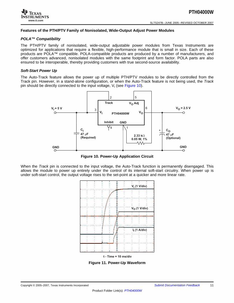
Soft-Start Power UpThe Auto-Track feature allows the power up of multiple PTH/PTV modules to be directly controlled from theTrack pin. However, in a stand-alone configuration, or when the Auto-Track feature is not being used, the Trackpin should be directly connected to the input voltage, VI (see Figure 10).
Figure 10. Power-Up Application Circuit
When the Track pin is connected to the input voltage, the Auto-Track function is permanently disengaged. Thisallows the module to power up entirely under the control of its internal soft-start circuitry. When power up isunder soft-start control, the output voltage rises to the set-point at a quicker and more linear rate.
Figure 11. Power-Up Waveform
Copyright © 2005–2007, Texas Instruments Incorporated Submit Documentation Feedback 11
Product Folder Link(s): PTH04000W
www.ti.com
Current Limit Protection
Thermal Shutdown
Output On/Off Inhibit
PTH04000W
SLTS247B–JUNE 2005–REVISED OCTOBER 2007
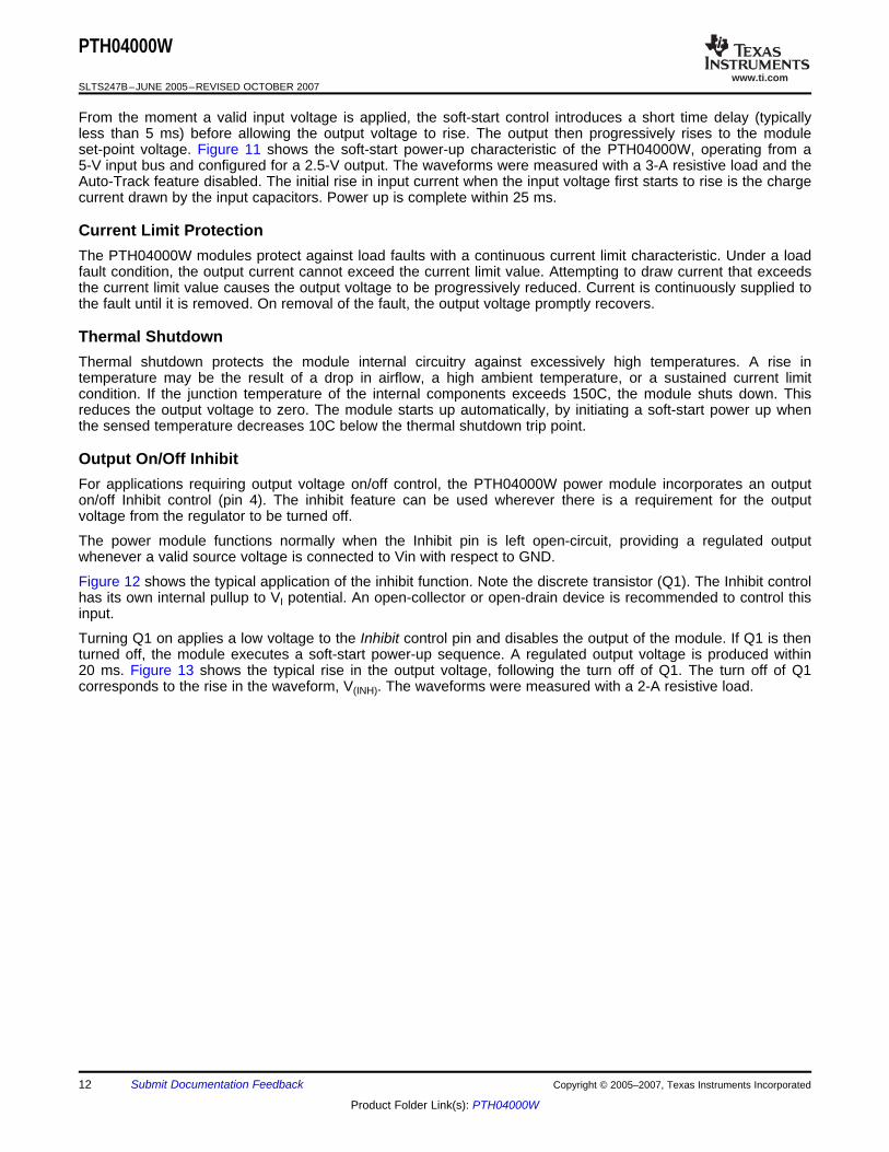
From the moment a valid input voltage is applied, the soft-start control introduces a short time delay (typicallyless than 5 ms) before allowing the output voltage to rise. The output then progressively rises to the moduleset-point voltage. Figure 11 shows the soft-start power-up characteristic of the PTH04000W, operating from a5-V input bus and configured for a 2.5-V output. The waveforms were measured with a 3-A resistive load and theAuto-Track feature disabled. The initial rise in input current when the input voltage first starts to rise is the chargecurrent drawn by the input capacitors. Power up is complete within 25 ms.
The PTH04000W modules protect against load faults with a continuous current limit characteristic. Under a loadfault condition, the output current cannot exceed the current limit value. Attempting to draw current that exceedsthe current limit value causes the output voltage to be progressively reduced. Current is continuously supplied tothe fault until it is removed. On removal of the fault, the output voltage promptly recovers.
Thermal shutdown protects the module internal circuitry against excessively high temperatures. A rise intemperature may be the result of a drop in airflow, a high ambient temperature, or a sustained current limitcondition. If the junction temperature of the internal components exceeds 150C, the module shuts down. Thisreduces the output voltage to zero. The module starts up automatically, by initiating a soft-start power up whenthe sensed temperature decreases 10C below the thermal shutdown trip point.
For applications requiring output voltage on/off control, the PTH04000W power module incorporates an outputon/off Inhibit control (pin 4). The inhibit feature can be used wherever there is a requirement for the outputvoltage from the regulator to be turned off.
The power module functions normally when the Inhibit pin is left open-circuit, providing a regulated outputwhenever a valid source voltage is connected to Vin with respect to GND.
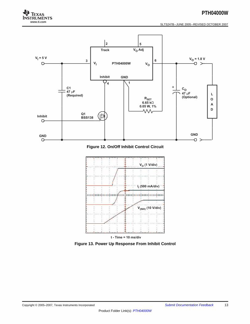
Figure 12 shows the typical application of the inhibit function. Note the discrete transistor (Q1). The Inhibit controlhas its own internal pullup to VI potential. An open-collector or open-drain device is recommended to control thisinput.
Turning Q1 on applies a low voltage to the Inhibit control pin and disables the output of the module. If Q1 is thenturned off, the module executes a soft-start power-up sequence. A regulated output voltage is produced within20 ms. Figure 13 shows the typical rise in the output voltage, following the turn off of Q1. The turn off of Q1corresponds to the rise in the waveform, V(INH). The waveforms were measured with a 2-A resistive load.
12 Submit Documentation Feedback Copyright © 2005–2007, Texas Instruments Incorporated
Product Folder Link(s): PTH04000W
www.ti.com
+
L
O
A
D
PTH04000W
R
6.65 k0.05 W, 1%
SET
Ù
V = 5 VI V = 1.8 VO
GND
Track
Inhibit
Inhibit
GND
GND
V AdjO
VOVI
3
2 5
6
14
C147 F(Required)
µC
47 F(Optional)
O
µ
Q1BSS138
t - Time = 10 ms/div
V (1 V/div)O
I (500 mA/div)I
V (10 V/div)(INH)
PTH04000W
SLTS247B–JUNE 2005–REVISED OCTOBER 2007
Figure 12. On/Off Inhibit Control Circuit
Figure 13. Power Up Response From Inhibit Control
Copyright © 2005–2007, Texas Instruments Incorporated Submit Documentation Feedback 13
Product Folder Link(s): PTH04000W
www.ti.com
Auto-Track™ Function
How Auto-Track™ Works
U1
C6
+
U2
C4
0.1 µF
GND
MR
CT
6
5
3
4
1
2C3
4700 pF
C21
5
6
4
GNDInhibit
2
1
5
6
4
GNDInhibit
2
C5
C1
3
3
+
5 V
Track
Track
*Use TPS3808G33 with 3.3-V input modules.
475 W
5.49 kW
VI
VI
VO
VO
PTH04000W
U3TPS3808G50*
PTH05050W
V 1 = 3.3 VO
V 2 = 1.8 VO
V AdjO
V AdjO
0 V
SENSE
RESET
VCC
PTH04000W
SLTS247B–JUNE 2005–REVISED OCTOBER 2007
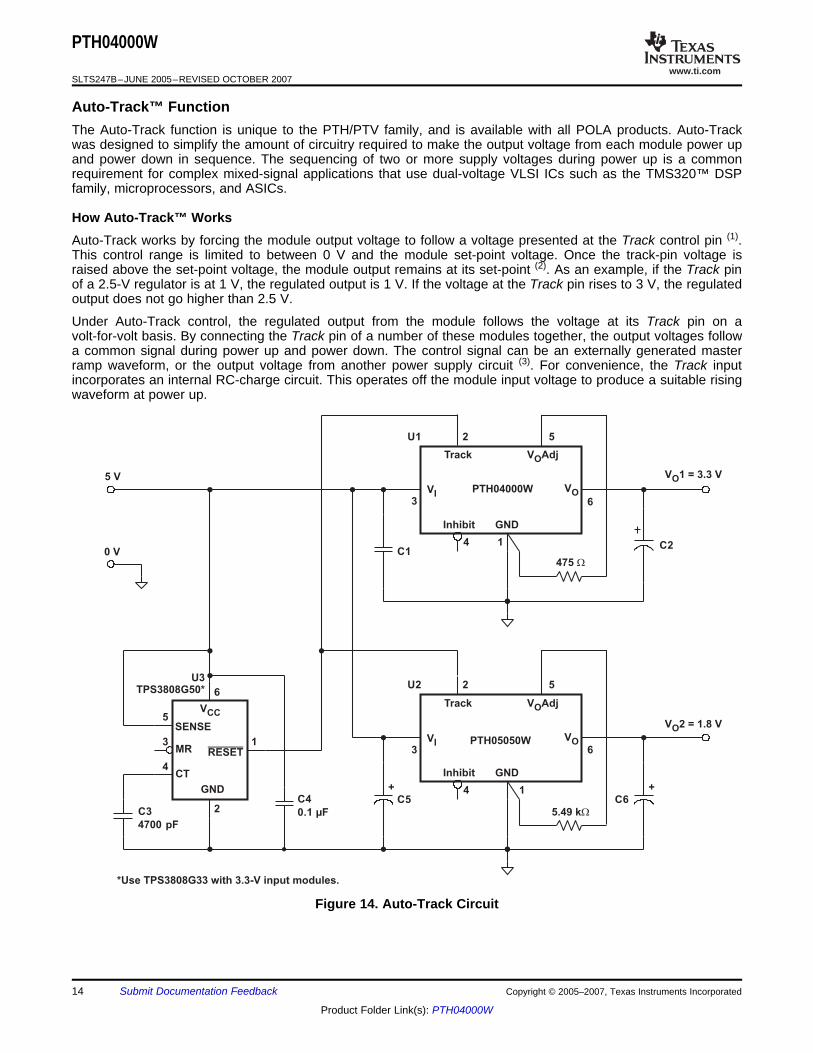
The Auto-Track function is unique to the PTH/PTV family, and is available with all POLA products. Auto-Trackwas designed to simplify the amount of circuitry required to make the output voltage from each module power upand power down in sequence. The sequencing of two or more supply voltages during power up is a commonrequirement for complex mixed-signal applications that use dual-voltage VLSI ICs such as the TMS320™ DSPfamily, microprocessors, and ASICs.
Auto-Track works by forcing the module output voltage to follow a voltage presented at the Track control pin (1).This control range is limited to between 0 V and the module set-point voltage. Once the track-pin voltage israised above the set-point voltage, the module output remains at its set-point (2). As an example, if the Track pinof a 2.5-V regulator is at 1 V, the regulated output is 1 V. If the voltage at the Track pin rises to 3 V, the regulatedoutput does not go higher than 2.5 V.
Under Auto-Track control, the regulated output from the module follows the voltage at its Track pin on avolt-for-volt basis. By connecting the Track pin of a number of these modules together, the output voltages followa common signal during power up and power down. The control signal can be an externally generated masterramp waveform, or the output voltage from another power supply circuit (3). For convenience, the Track inputincorporates an internal RC-charge circuit. This operates off the module input voltage to produce a suitable risingwaveform at power up.
Figure 14. Auto-Track Circuit
14 Submit Documentation Feedback Copyright © 2005–2007, Texas Instruments Incorporated
Product Folder Link(s): PTH04000W
www.ti.com
t - Time = 400 s/divm
V (1 V/div)(TRK)
V 1 (1 V/div)O
V 2 (1 V/div)O
t - Time = 10 ms/div
V (1 V/div)(TRK)
V 1 (1 V/div)O
V 2 (1 V/div)O
Typical Application
PTH04000W
SLTS247B–JUNE 2005–REVISED OCTOBER 2007
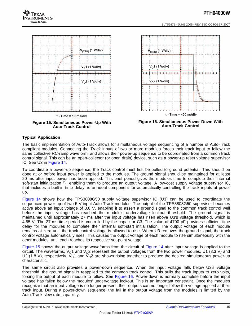
Figure 16. Simultaneous Power-Down WithFigure 15. Simultaneous Power-Up WithAuto-Track ControlAuto-Track Control
The basic implementation of Auto-Track allows for simultaneous voltage sequencing of a number of Auto-Trackcompliant modules. Connecting the Track inputs of two or more modules forces their track input to follow thesame collective RC-ramp waveform, and allows their power-up sequence to be coordinated from a common trackcontrol signal. This can be an open-collector (or open drain) device, such as a power-up reset voltage supervisorIC. See U3 in Figure 14.
To coordinate a power-up sequence, the Track control must first be pulled to ground potential. This should bedone at or before input power is applied to the modules. The ground signal should be maintained for at least20 ms after input power has been applied. This brief period gives the modules time to complete their internalsoft-start initialization (4), enabling them to produce an output voltage. A low-cost supply voltage supervisor IC,that includes a built-in time delay, is an ideal component for automatically controlling the track inputs at powerup.
Figure 14 shows how the TPS3808G50 supply voltage supervisor IC (U3) can be used to coordinate thesequenced power-up of two 5-V input Auto-Track modules. The output of the TPS3808G50 supervisor becomesactive above an input voltage of 0.8 V, enabling it to assert a ground signal to the common track control wellbefore the input voltage has reached the module's undervoltage lockout threshold. The ground signal ismaintained until approximately 27 ms after the input voltage has risen above U3's voltage threshold, which is4.65 V. The 27-ms time period is controlled by the capacitor C3. The value of 4700 pF provides sufficient timedelay for the modules to complete their internal soft-start initialization. The output voltage of each moduleremains at zero until the track control voltage is allowed to rise. When U3 removes the ground signal, the trackcontrol voltage automatically rises. This causes the output voltage of each module to rise simultaneously with theother modules, until each reaches its respective set-point voltage.
Figure 15 shows the output voltage waveforms from the circuit of Figure 14 after input voltage is applied to thecircuit. The waveforms, VO1 and VO2 represent the output voltages from the two power modules, U1 (3.3 V) andU2 (1.8 V), respectively. VO1 and VO2 are shown rising together to produce the desired simultaneous power-upcharacteristic.
The same circuit also provides a power-down sequence. When the input voltage falls below U3's voltagethreshold, the ground signal is reapplied to the common track control. This pulls the track inputs to zero volts,forcing the output of each module to follow. See Figure 16. Power-down is normally complete before the inputvoltage has fallen below the modules' undervoltage lockout. This is an important constraint. Once the modulesrecognize that an input voltage is no longer present, their outputs can no longer follow the voltage applied at theirtrack input. During a power-down sequence, the fall in the output voltage from the modules is limited by theAuto-Track slew rate capability.
Copyright © 2005–2007, Texas Instruments Incorporated Submit Documentation Feedback 15
Product Folder Link(s): PTH04000W
www.ti.com
Notes on Use of Auto-Track™
PTH04000W
SLTS247B–JUNE 2005–REVISED OCTOBER 2007
1. The Auto-Track function tracks almost any voltage ramp during power up, and is compatible with rampspeeds of up to 1 V/ms.
2. The Track pin voltage must be allowed to rise above the module set-point voltage before the moduleregulates at its adjusted set-point voltage.
3. The absolute maximum voltage that may be applied to the Track pin is the input voltage VI.4. The module cannot follow a voltage at its track control input until it has completed its soft-start initialization.
This takes about 20 ms from the time that a valid voltage has been applied to its input. During this period, itis recommended that the Track pin be held at ground potential.
5. The Auto-Track function is disabled by connecting the Track pin to the input voltage (VI). When Auto-Track isdisabled, the output voltage rises at a quicker and more linear rate after input power has been applied.
16 Submit Documentation Feedback Copyright © 2005–2007, Texas Instruments Incorporated
Product Folder Link(s): PTH04000W
PACKAGE OPTION ADDENDUM
www.ti.com 27-Apr-2017
Addendum-Page 1
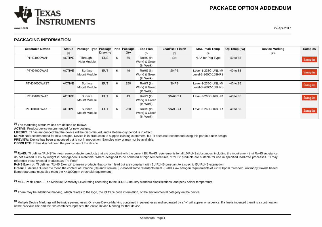
PACKAGING INFORMATION
Orderable Device Status(1)
Package Type PackageDrawing
Pins PackageQty
Eco Plan(2)
Lead/Ball Finish(6)
MSL Peak Temp(3)
Op Temp (°C) Device Marking(4/5)
Samples
PTH04000WAH ACTIVE Through-Hole Module
EUS 6 56 RoHS (InWork) & Green
(In Work)
SN N / A for Pkg Type -40 to 85
PTH04000WAS ACTIVE SurfaceMount Module
EUT 6 49 RoHS (InWork) & Green
(In Work)
SNPB Level-1-235C-UNLIM/Level-3-260C-168HRS
-40 to 85
PTH04000WAST ACTIVE SurfaceMount Module
EUT 6 250 RoHS (InWork) & Green
(In Work)
SNPB Level-1-235C-UNLIM/Level-3-260C-168HRS
-40 to 85
PTH04000WAZ ACTIVE SurfaceMount Module
EUT 6 49 RoHS (InWork) & Green
(In Work)
SNAGCU Level-3-260C-168 HR -40 to 85
PTH04000WAZT ACTIVE SurfaceMount Module
EUT 6 250 RoHS (InWork) & Green
(In Work)
SNAGCU Level-3-260C-168 HR -40 to 85
(1) The marketing status values are defined as follows:ACTIVE: Product device recommended for new designs.LIFEBUY: TI has announced that the device will be discontinued, and a lifetime-buy period is in effect.NRND: Not recommended for new designs. Device is in production to support existing customers, but TI does not recommend using this part in a new design.PREVIEW: Device has been announced but is not in production. Samples may or may not be available.OBSOLETE: TI has discontinued the production of the device.
(2) RoHS: TI defines "RoHS" to mean semiconductor products that are compliant with the current EU RoHS requirements for all 10 RoHS substances, including the requirement that RoHS substancedo not exceed 0.1% by weight in homogeneous materials. Where designed to be soldered at high temperatures, "RoHS" products are suitable for use in specified lead-free processes. TI mayreference these types of products as "Pb-Free".RoHS Exempt: TI defines "RoHS Exempt" to mean products that contain lead but are compliant with EU RoHS pursuant to a specific EU RoHS exemption.Green: TI defines "Green" to mean the content of Chlorine (Cl) and Bromine (Br) based flame retardants meet JS709B low halogen requirements of <=1000ppm threshold. Antimony trioxide basedflame retardants must also meet the <=1000ppm threshold requirement.
(3) MSL, Peak Temp. - The Moisture Sensitivity Level rating according to the JEDEC industry standard classifications, and peak solder temperature.
(4) There may be additional marking, which relates to the logo, the lot trace code information, or the environmental category on the device.
(5) Multiple Device Markings will be inside parentheses. Only one Device Marking contained in parentheses and separated by a "~" will appear on a device. If a line is indented then it is a continuationof the previous line and the two combined represent the entire Device Marking for that device.
PACKAGE OPTION ADDENDUM
www.ti.com 27-Apr-2017
Addendum-Page 2
(6) Lead/Ball Finish - Orderable Devices may have multiple material finish options. Finish options are separated by a vertical ruled line. Lead/Ball Finish values may wrap to two lines if the finishvalue exceeds the maximum column width.
Important Information and Disclaimer:The information provided on this page represents TI's knowledge and belief as of the date that it is provided. TI bases its knowledge and belief on informationprovided by third parties, and makes no representation or warranty as to the accuracy of such information. Efforts are underway to better integrate information from third parties. TI has taken andcontinues to take reasonable steps to provide representative and accurate information but may not have conducted destructive testing or chemical analysis on incoming materials and chemicals.TI and TI suppliers consider certain information to be proprietary, and thus CAS numbers and other limited information may not be available for release.
In no event shall TI's liability arising out of such information exceed the total purchase price of the TI part(s) at issue in this document sold by TI to Customer on an annual basis.
IMPORTANT NOTICE
Texas Instruments Incorporated (TI) reserves the right to make corrections, enhancements, improvements and other changes to itssemiconductor products and services per JESD46, latest issue, and to discontinue any product or service per JESD48, latest issue. Buyersshould obtain the latest relevant information before placing orders and should verify that such information is current and complete.TI’s published terms of sale for semiconductor products (http://www.ti.com/sc/docs/stdterms.htm) apply to the sale of packaged integratedcircuit products that TI has qualified and released to market. Additional terms may apply to the use or sale of other types of TI products andservices.Reproduction of significant portions of TI information in TI data sheets is permissible only if reproduction is without alteration and isaccompanied by all associated warranties, conditions, limitations, and notices. TI is not responsible or liable for such reproduceddocumentation. Information of third parties may be subject to additional restrictions. Resale of TI products or services with statementsdifferent from or beyond the parameters stated by TI for that product or service voids all express and any implied warranties for theassociated TI product or service and is an unfair and deceptive business practice. TI is not responsible or liable for any such statements.Buyers and others who are developing systems that incorporate TI products (collectively, “Designers”) understand and agree that Designersremain responsible for using their independent analysis, evaluation and judgment in designing their applications and that Designers havefull and exclusive responsibility to assure the safety of Designers' applications and compliance of their applications (and of all TI productsused in or for Designers’ applications) with all applicable regulations, laws and other applicable requirements. Designer represents that, withrespect to their applications, Designer has all the necessary expertise to create and implement safeguards that (1) anticipate dangerousconsequences of failures, (2) monitor failures and their consequences, and (3) lessen the likelihood of failures that might cause harm andtake appropriate actions. Designer agrees that prior to using or distributing any applications that include TI products, Designer willthoroughly test such applications and the functionality of such TI products as used in such applications.TI’s provision of technical, application or other design advice, quality characterization, reliability data or other services or information,including, but not limited to, reference designs and materials relating to evaluation modules, (collectively, “TI Resources”) are intended toassist designers who are developing applications that incorporate TI products; by downloading, accessing or using TI Resources in anyway, Designer (individually or, if Designer is acting on behalf of a company, Designer’s company) agrees to use any particular TI Resourcesolely for this purpose and subject to the terms of this Notice.TI’s provision of TI Resources does not expand or otherwise alter TI’s applicable published warranties or warranty disclaimers for TIproducts, and no additional obligations or liabilities arise from TI providing such TI Resources. TI reserves the right to make corrections,enhancements, improvements and other changes to its TI Resources. TI has not conducted any testing other than that specificallydescribed in the published documentation for a particular TI Resource.Designer is authorized to use, copy and modify any individual TI Resource only in connection with the development of applications thatinclude the TI product(s) identified in such TI Resource. NO OTHER LICENSE, EXPRESS OR IMPLIED, BY ESTOPPEL OR OTHERWISETO ANY OTHER TI INTELLECTUAL PROPERTY RIGHT, AND NO LICENSE TO ANY TECHNOLOGY OR INTELLECTUAL PROPERTYRIGHT OF TI OR ANY THIRD PARTY IS GRANTED HEREIN, including but not limited to any patent right, copyright, mask work right, orother intellectual property right relating to any combination, machine, or process in which TI products or services are used. Informationregarding or referencing third-party products or services does not constitute a license to use such products or services, or a warranty orendorsement thereof. Use of TI Resources may require a license from a third party under the patents or other intellectual property of thethird party, or a license from TI under the patents or other intellectual property of TI.TI RESOURCES ARE PROVIDED “AS IS” AND WITH ALL FAULTS. TI DISCLAIMS ALL OTHER WARRANTIES ORREPRESENTATIONS, EXPRESS OR IMPLIED, REGARDING RESOURCES OR USE THEREOF, INCLUDING BUT NOT LIMITED TOACCURACY OR COMPLETENESS, TITLE, ANY EPIDEMIC FAILURE WARRANTY AND ANY IMPLIED WARRANTIES OFMERCHANTABILITY, FITNESS FOR A PARTICULAR PURPOSE, AND NON-INFRINGEMENT OF ANY THIRD PARTY INTELLECTUALPROPERTY RIGHTS. TI SHALL NOT BE LIABLE FOR AND SHALL NOT DEFEND OR INDEMNIFY DESIGNER AGAINST ANY CLAIM,INCLUDING BUT NOT LIMITED TO ANY INFRINGEMENT CLAIM THAT RELATES TO OR IS BASED ON ANY COMBINATION OFPRODUCTS EVEN IF DESCRIBED IN TI RESOURCES OR OTHERWISE. IN NO EVENT SHALL TI BE LIABLE FOR ANY ACTUAL,DIRECT, SPECIAL, COLLATERAL, INDIRECT, PUNITIVE, INCIDENTAL, CONSEQUENTIAL OR EXEMPLARY DAMAGES INCONNECTION WITH OR ARISING OUT OF TI RESOURCES OR USE THEREOF, AND REGARDLESS OF WHETHER TI HAS BEENADVISED OF THE POSSIBILITY OF SUCH DAMAGES.Unless TI has explicitly designated an individual product as meeting the requirements of a particular industry standard (e.g., ISO/TS 16949and ISO 26262), TI is not responsible for any failure to meet such industry standard requirements.Where TI specifically promotes products as facilitating functional safety or as compliant with industry functional safety standards, suchproducts are intended to help enable customers to design and create their own applications that meet applicable functional safety standardsand requirements. Using products in an application does not by itself establish any safety features in the application. Designers mustensure compliance with safety-related requirements and standards applicable to their applications. Designer may not use any TI products inlife-critical medical equipment unless authorized officers of the parties have executed a special contract specifically governing such use.Life-critical medical equipment is medical equipment where failure of such equipment would cause serious bodily injury or death (e.g., lifesupport, pacemakers, defibrillators, heart pumps, neurostimulators, and implantables). Such equipment includes, without limitation, allmedical devices identified by the U.S. Food and Drug Administration as Class III devices and equivalent classifications outside the U.S.TI may expressly designate certain products as completing a particular qualification (e.g., Q100, Military Grade, or Enhanced Product).Designers agree that it has the necessary expertise to select the product with the appropriate qualification designation for their applicationsand that proper product selection is at Designers’ own risk. Designers are solely responsible for compliance with all legal and regulatoryrequirements in connection with such selection.Designer will fully indemnify TI and its representatives against any damages, costs, losses, and/or liabilities arising out of Designer’s non-compliance with the terms and provisions of this Notice.
Mailing Address: Texas Instruments, Post Office Box 655303, Dallas, Texas 75265Copyright © 2017, Texas Instruments Incorporated