Embed Size (px)
Citation preview
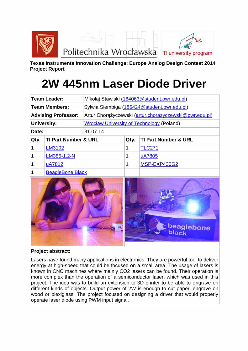
Texas Instruments Innovation Challenge: Europe Analog Design Contest 2014 Project Report
2W 445nm Laser Diode Driver Team Leader: Mikołaj Stawiski ([email protected])
Team Members: Team Sylwia Siembiga ([email protected])
Advising Professor: Artur Chorążyczewski ([email protected])
University: Wrocław University of Technology (Poland)
Date: 31.07.14
Qty. TI Part Number & URL Qty. TI Part Number & URL
1 LM3102 1 TLC271
1 LM385-1.2-N 1 uA7805
1 uA7812 1 MSP-EXP430G2
1 BeagleBone Black
Project abstract:
Lasers have found many applications in electronics. They are powerful tool to deliver energy at high-speed that could be focused on a small area. The usage of lasers is known in CNC machines where mainly CO2 lasers can be found. Their operation is more complex than the operation of a semiconductor laser, which was used in this project. The idea was to build an extension to 3D printer to be able to engrave on different kinds of objects. Output power of 2W is enough to cut paper, engrave on wood or plexiglass. The project focused on designing a driver that would properly operate laser diode using PWM input signal.
2
1. Introduction and Motivation
An extension to existing device was needed to expand its capabilities. The device was a 3-axis CNC machine used mainly as a 3D printer, but with different “heads” it could be used as something else. Laser head was proposed as one of the extensions and we took the challenge. Due to limited space and project requirements we have decided to use 2W laser diode, that would fit in a heatsink in the machine. Those 2W 445nm diodes are available on the market for a reasonable price, so they were targeted. The laser power was to be modulated using isolated PWM input signal for obvious reasons of turning the laser on and off, but also to enable controlling the average laser power with PWM duty cycle. 2. Theoretical Background
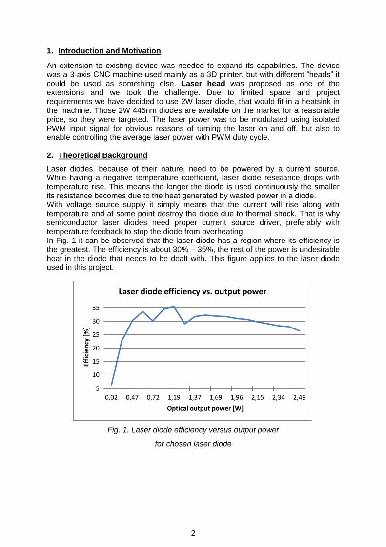
Laser diodes, because of their nature, need to be powered by a current source. While having a negative temperature coefficient, laser diode resistance drops with temperature rise. This means the longer the diode is used continuously the smaller its resistance becomes due to the heat generated by wasted power in a diode. With voltage source supply it simply means that the current will rise along with temperature and at some point destroy the diode due to thermal shock. That is why semiconductor laser diodes need proper current source driver, preferably with temperature feedback to stop the diode from overheating. In Fig. 1 it can be observed that the laser diode has a region where its efficiency is the greatest. The efficiency is about 30% – 35%, the rest of the power is undesirable heat in the diode that needs to be dealt with. This figure applies to the laser diode used in this project.
Fig. 1. Laser diode efficiency versus output power
for chosen laser diode
5
10
15
20
25
30
35
0,02 0,47 0,72 1,19 1,37 1,69 1,96 2,15 2,34 2,49
Effi
cien
cy [
%]
Optical output power [W]
Laser diode efficiency vs. output power
3
3. Implementation
Firstly we came up with project requirements to be sure of our goals and milestones. They come as following:
Supply voltage of 24VDC – this is due to that voltage being an industrial standard, as well as its availability in the 3D printer
PWM input – we want to modulate the output laser power using PWM signal, the duty cycle could change from 0% to 75% and the maximum frequency of 10kHz
Isolated input – galvanic isolation of 1kV between the input signal and driver
Adjustable laser current – in form of a potentiometer, to be able to set maximum laser current
Laser current rising slowly – to avoid overshoots
Laser diode forward voltage drop up to 5V – needed to design proper current source, the diode used has up to 4.6V forward drop
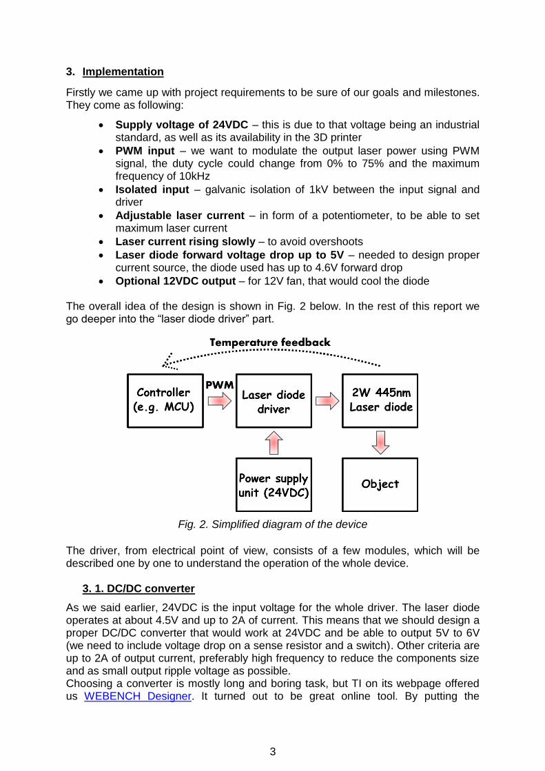
Optional 12VDC output – for 12V fan, that would cool the diode The overall idea of the design is shown in Fig. 2 below. In the rest of this report we go deeper into the “laser diode driver” part.
Fig. 2. Simplified diagram of the device
The driver, from electrical point of view, consists of a few modules, which will be described one by one to understand the operation of the whole device.
3. 1. DC/DC converter
As we said earlier, 24VDC is the input voltage for the whole driver. The laser diode operates at about 4.5V and up to 2A of current. This means that we should design a proper DC/DC converter that would work at 24VDC and be able to output 5V to 6V (we need to include voltage drop on a sense resistor and a switch). Other criteria are up to 2A of output current, preferably high frequency to reduce the components size and as small output ripple voltage as possible. Choosing a converter is mostly long and boring task, but TI on its webpage offered us WEBENCH Designer. It turned out to be great online tool. By putting the
4
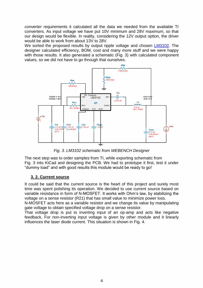
converter requirements it calculated all the data we needed from the available TI converters. As input voltage we have put 10V minimum and 28V maximum, so that our design would be flexible. In reality, considering the 12V output option, the driver would be able to work from about 13V to 28V. We sorted the proposed results by output ripple voltage and chosen LM3102. The designer calculated efficiency, BOM, cost and many more stuff and we were happy with those results. It also generated a schematic (Fig. 3) with calculated component values, so we did not have to go through that ourselves.
Fig. 3. LM3102 schematic from WEBENCH Designer
The next step was to order samples from TI, while exporting schematic from Fig. 3 into KiCad and designing the PCB. We had to prototype it first, test it under “dummy load” and with good results this module would be ready to go!
3. 2. Current source
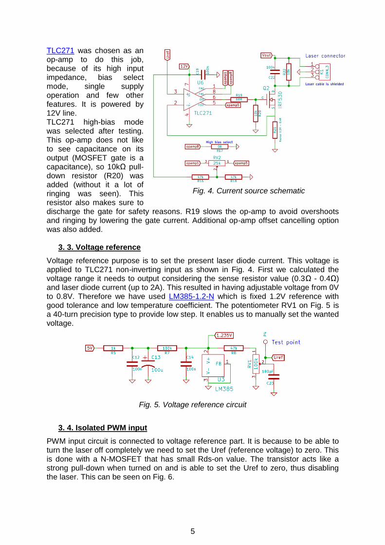
It could be said that the current source is the heart of this project and surely most time was spent polishing its operation. We decided to use current source based on variable resistance in form of N-MOSFET. It works with Ohm’s law, by stabilizing the voltage on a sense resistor (R21) that has small value to minimize power loss. N-MOSFET acts here as a variable resistor and we change its value by manipulating gate voltage to obtain specified voltage drop on a sense resistor. That voltage drop is put to inverting input of an op-amp and acts like negative feedback. For non-inverting input voltage is given by other module and it linearly influences the laser diode current. This situation is shown in Fig. 4.
5
TLC271 was chosen as an op-amp to do this job, because of its high input impedance, bias select mode, single supply operation and few other features. It is powered by 12V line. TLC271 high-bias mode was selected after testing. This op-amp does not like to see capacitance on its output (MOSFET gate is a capacitance), so 10kΩ pull-down resistor (R20) was added (without it a lot of ringing was seen). This resistor also makes sure to discharge the gate for safety reasons. R19 slows the op-amp to avoid overshoots and ringing by lowering the gate current. Additional op-amp offset cancelling option was also added.
3. 3. Voltage reference
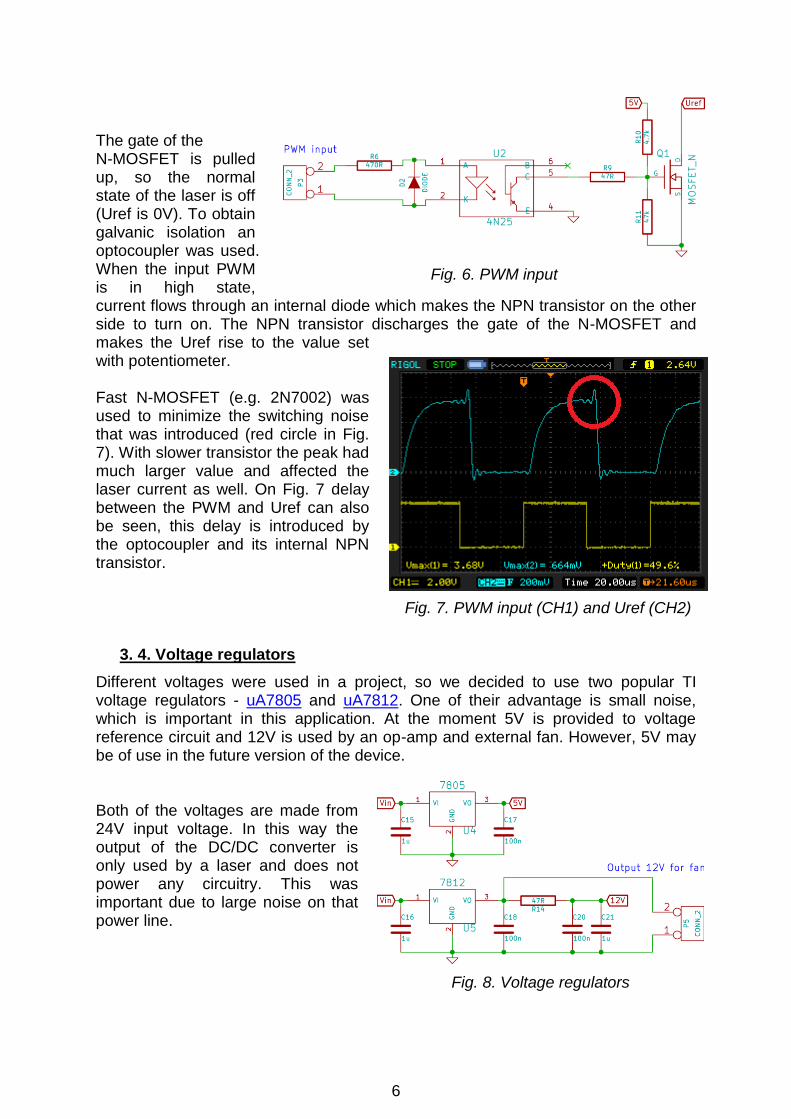
Voltage reference purpose is to set the present laser diode current. This voltage is applied to TLC271 non-inverting input as shown in Fig. 4. First we calculated the voltage range it needs to output considering the sense resistor value (0.3Ω - 0.4Ω) and laser diode current (up to 2A). This resulted in having adjustable voltage from 0V to 0.8V. Therefore we have used LM385-1.2-N which is fixed 1.2V reference with good tolerance and low temperature coefficient. The potentiometer RV1 on Fig. 5 is a 40-turn precision type to provide low step. It enables us to manually set the wanted voltage.
Fig. 5. Voltage reference circuit
3. 4. Isolated PWM input
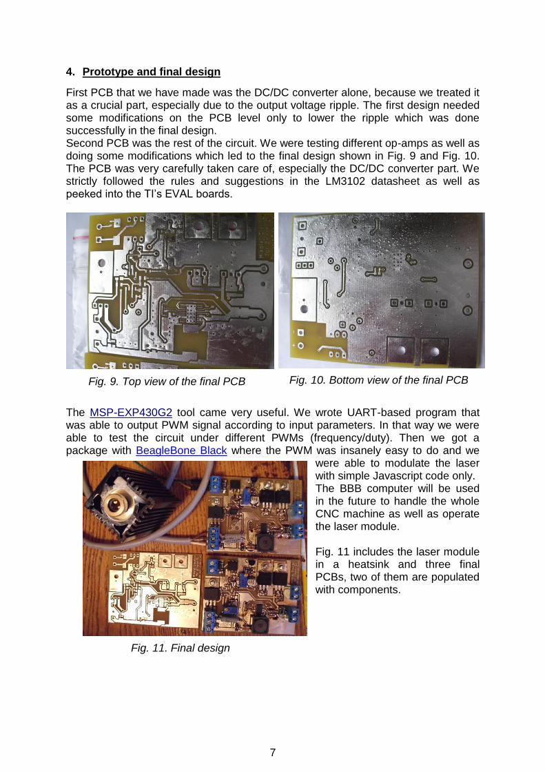
PWM input circuit is connected to voltage reference part. It is because to be able to turn the laser off completely we need to set the Uref (reference voltage) to zero. This is done with a N-MOSFET that has small Rds-on value. The transistor acts like a strong pull-down when turned on and is able to set the Uref to zero, thus disabling the laser. This can be seen on Fig. 6.
Fig. 4. Current source schematic
6
The gate of the N-MOSFET is pulled up, so the normal state of the laser is off (Uref is 0V). To obtain galvanic isolation an optocoupler was used. When the input PWM is in high state, current flows through an internal diode which makes the NPN transistor on the other side to turn on. The NPN transistor discharges the gate of the N-MOSFET and makes the Uref rise to the value set with potentiometer. Fast N-MOSFET (e.g. 2N7002) was used to minimize the switching noise that was introduced (red circle in Fig. 7). With slower transistor the peak had much larger value and affected the laser current as well. On Fig. 7 delay between the PWM and Uref can also be seen, this delay is introduced by the optocoupler and its internal NPN transistor.
3. 4. Voltage regulators
Different voltages were used in a project, so we decided to use two popular TI voltage regulators - uA7805 and uA7812. One of their advantage is small noise, which is important in this application. At the moment 5V is provided to voltage reference circuit and 12V is used by an op-amp and external fan. However, 5V may be of use in the future version of the device. Both of the voltages are made from 24V input voltage. In this way the output of the DC/DC converter is only used by a laser and does not power any circuitry. This was important due to large noise on that power line.
Fig. 6. PWM input
Fig. 7. PWM input (CH1) and Uref (CH2)
Fig. 8. Voltage regulators
7
4. Prototype and final design
First PCB that we have made was the DC/DC converter alone, because we treated it as a crucial part, especially due to the output voltage ripple. The first design needed some modifications on the PCB level only to lower the ripple which was done successfully in the final design. Second PCB was the rest of the circuit. We were testing different op-amps as well as doing some modifications which led to the final design shown in Fig. 9 and Fig. 10. The PCB was very carefully taken care of, especially the DC/DC converter part. We strictly followed the rules and suggestions in the LM3102 datasheet as well as peeked into the TI’s EVAL boards.
Fig. 9. Top view of the final PCB
Fig. 10. Bottom view of the final PCB
The MSP-EXP430G2 tool came very useful. We wrote UART-based program that was able to output PWM signal according to input parameters. In that way we were able to test the circuit under different PWMs (frequency/duty). Then we got a package with BeagleBone Black where the PWM was insanely easy to do and we
were able to modulate the laser with simple Javascript code only. The BBB computer will be used in the future to handle the whole CNC machine as well as operate the laser module. Fig. 11 includes the laser module in a heatsink and three final PCBs, two of them are populated with components.
Fig. 11. Final design
8
5. Results
After long tests on “dummy load”, which was a few high-current diodes in series with a comparable voltage drop to a laser, we have achieved the expected outcome with a real laser diode. At this point it is worth mentioning that we have used proper safety googles that provide total internal reflection for the 445nm wavelength. With the googles the laser spot on an object is still seen probably due to other wavelengths it radiates. Fig. 12 illustrates the driver being modulated by MSP430 board. In the background a wooden, burned test ground can be seen.
Fig. 12. MSP430 board modulating the laser
The results achieved are best seen on an oscilloscope. Due to strong magnetic field produced by the DC/DC converter, data acquisition was a bit harder than usual. To deal with that problem, probe’s ground clip was omitted to get the shortest ground path possible. On Fig. 14 DC/DC converter output voltage ripple can be observed with no load connected (laser in off state). On Fig. 15 is the opposite situation where laser is fully on (PWM at 100%).
Fig. 13. LM3102 output voltage ripple without load (laser off)
Fig. 14. LM3102 output voltage ripple with laser continuously on
9
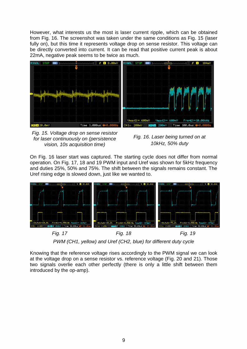
However, what interests us the most is laser current ripple, which can be obtained from Fig. 16. The screenshot was taken under the same conditions as Fig. 15 (laser fully on), but this time it represents voltage drop on sense resistor. This voltage can be directly converted into current. It can be read that positive current peak is about 22mA, negative peak seems to be twice as much.
Fig. 15. Voltage drop on sense resistor for laser continuously on (persistence
vision, 10s acquisition time)
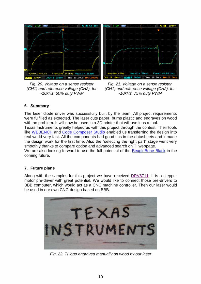
On Fig. 16 laser start was captured. The starting cycle does not differ from normal operation. On Fig. 17, 18 and 19 PWM input and Uref was shown for 5kHz frequency and duties 25%, 50% and 75%. The shift between the signals remains constant. The Uref rising edge is slowed down, just like we wanted to.
Fig. 17
Fig. 18
Fig. 19
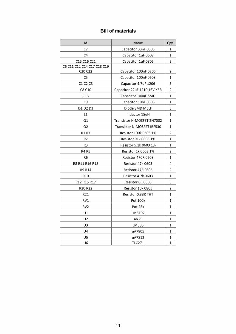
PWM (CH1, yellow) and Uref (CH2, blue) for different duty cycle Knowing that the reference voltage rises accordingly to the PWM signal we can look at the voltage drop on a sense resistor vs. reference voltage (Fig. 20 and 21). Those two signals overlie each other perfectly (there is only a little shift between them introduced by the op-amp).
Fig. 16. Laser being turned on at
10kHz, 50% duty
10
Fig. 20. Voltage on a sense resistor (CH1) and reference voltage (CH2), for
~10kHz, 50% duty PWM
Fig. 21. Voltage on a sense resistor (CH1) and reference voltage (CH2), for
~10kHz, 75% duty PWM
6. Summary
The laser diode driver was successfully built by the team. All project requirements were fulfilled as expected. The laser cuts paper, burns plastic and engraves on wood with no problem. It will now be used in a 3D printer that will use it as a tool. Texas Instruments greatly helped us with this project through the contest. Their tools like WEBENCH and Code Composer Studio enabled us transferring the design into real world very fast. All the components had good tips in the datasheets and it made the design work for the first time. Also the “selecting the right part” stage went very smoothly thanks to compare option and advanced search on TI webpage. We are also looking forward to use the full potential of the BeagleBone Black in the coming future.
7. Future plans
Along with the samples for this project we have received DRV8711. It is a stepper motor pre-driver with great potential. We would like to connect those pre-drivers to BBB computer, which would act as a CNC machine controller. Then our laser would be used in our own CNC-design based on BBB.
Fig. 22. TI logo engraved manually on wood by our laser
11
Bill of materials
Id Name Qty.
C7 Capacitor 33nF 0603 1
C4 Capacitor 1uF 0603 1
C15 C16 C21 Capacitor 1uF 0805 3
C6 C11 C12 C14 C17 C18 C19 C20 C22 Capacitor 100nF 0805 9
C5 Capacitor 100nF 0603 1
C1 C2 C3 Capacitor 4.7uF 1206 3
C8 C10 Capacitor 22uF 1210 16V X5R 2
C13 Capacitor 100uF SMD 1
C9 Capacitor 10nF 0603 1
D1 D2 D3 Diode SMD MELF 3
L1 Inductor 15uH 1
Q1 Transistor N-MOSFET 2N7002 1
Q2 Transistor N-MOSFET IRF530 1
R1 R7 Resistor 100k 0603 1% 2
R2 Resistor 91k 0603 1% 1
R3 Resistor 5.1k 0603 1% 1
R4 R5 Resistor 1k 0603 1% 2
R6 Resistor 470R 0603 1
R8 R11 R16 R18 Resistor 47k 0603 4
R9 R14 Resistor 47R 0805 2
R10 Resistor 4.7k 0603 1
R12 R15 R17 Resistor 0R 0805 3
R20 R22 Resistor 10k 0805 2
R21 Resistor 0.33R THT 1
RV1 Pot 100k 1
RV2 Pot 25k 1
U1 LM3102 1
U2 4N25 1
U3 LM385 1
U4 uA7805 1
U5 uA7812 1
U6 TLC271 1

IMPORTANT NOTICETexas Instruments Incorporated and its subsidiaries (TI) reserve the right to make corrections, enhancements, improvements and otherchanges to its semiconductor products and services per JESD46, latest issue, and to discontinue any product or service per JESD48, latestissue. Buyers should obtain the latest relevant information before placing orders and should verify that such information is current andcomplete. All semiconductor products (also referred to herein as “components”) are sold subject to TI’s terms and conditions of salesupplied at the time of order acknowledgment.TI warrants performance of its components to the specifications applicable at the time of sale, in accordance with the warranty in TI’s termsand conditions of sale of semiconductor products. Testing and other quality control techniques are used to the extent TI deems necessaryto support this warranty. Except where mandated by applicable law, testing of all parameters of each component is not necessarilyperformed.TI assumes no liability for applications assistance or the design of Buyers’ products. Buyers are responsible for their products andapplications using TI components. To minimize the risks associated with Buyers’ products and applications, Buyers should provideadequate design and operating safeguards.TI does not warrant or represent that any license, either express or implied, is granted under any patent right, copyright, mask work right, orother intellectual property right relating to any combination, machine, or process in which TI components or services are used. Informationpublished by TI regarding third-party products or services does not constitute a license to use such products or services or a warranty orendorsement thereof. Use of such information may require a license from a third party under the patents or other intellectual property of thethird party, or a license from TI under the patents or other intellectual property of TI.Reproduction of significant portions of TI information in TI data books or data sheets is permissible only if reproduction is without alterationand is accompanied by all associated warranties, conditions, limitations, and notices. TI is not responsible or liable for such altereddocumentation. Information of third parties may be subject to additional restrictions.Resale of TI components or services with statements different from or beyond the parameters stated by TI for that component or servicevoids all express and any implied warranties for the associated TI component or service and is an unfair and deceptive business practice.TI is not responsible or liable for any such statements.Buyer acknowledges and agrees that it is solely responsible for compliance with all legal, regulatory and safety-related requirementsconcerning its products, and any use of TI components in its applications, notwithstanding any applications-related information or supportthat may be provided by TI. Buyer represents and agrees that it has all the necessary expertise to create and implement safeguards whichanticipate dangerous consequences of failures, monitor failures and their consequences, lessen the likelihood of failures that might causeharm and take appropriate remedial actions. Buyer will fully indemnify TI and its representatives against any damages arising out of the useof any TI components in safety-critical applications.In some cases, TI components may be promoted specifically to facilitate safety-related applications. With such components, TI’s goal is tohelp enable customers to design and create their own end-product solutions that meet applicable functional safety standards andrequirements. Nonetheless, such components are subject to these terms.No TI components are authorized for use in FDA Class III (or similar life-critical medical equipment) unless authorized officers of the partieshave executed a special agreement specifically governing such use.Only those TI components which TI has specifically designated as military grade or “enhanced plastic” are designed and intended for use inmilitary/aerospace applications or environments. Buyer acknowledges and agrees that any military or aerospace use of TI componentswhich have not been so designated is solely at the Buyer's risk, and that Buyer is solely responsible for compliance with all legal andregulatory requirements in connection with such use.TI has specifically designated certain components as meeting ISO/TS16949 requirements, mainly for automotive use. In any case of use ofnon-designated products, TI will not be responsible for any failure to meet ISO/TS16949.Products ApplicationsAudio www.ti.com/audio Automotive and Transportation www.ti.com/automotiveAmplifiers amplifier.ti.com Communications and Telecom www.ti.com/communicationsData Converters dataconverter.ti.com Computers and Peripherals www.ti.com/computersDLP® Products www.dlp.com Consumer Electronics www.ti.com/consumer-appsDSP dsp.ti.com Energy and Lighting www.ti.com/energyClocks and Timers www.ti.com/clocks Industrial www.ti.com/industrialInterface interface.ti.com Medical www.ti.com/medicalLogic logic.ti.com Security www.ti.com/securityPower Mgmt power.ti.com Space, Avionics and Defense www.ti.com/space-avionics-defenseMicrocontrollers microcontroller.ti.com Video and Imaging www.ti.com/videoRFID www.ti-rfid.comOMAP Applications Processors www.ti.com/omap TI E2E Community e2e.ti.comWireless Connectivity www.ti.com/wirelessconnectivity
Mailing Address: Texas Instruments, Post Office Box 655303, Dallas, Texas 75265Copyright © 2014, Texas Instruments Incorporated


![API 2W [1993]](https://img.pdfslide.us/doc/110x75/577cd4db1a28ab9e78994d52/api-2w-1993.jpg)