Embed Size (px)
Citation preview
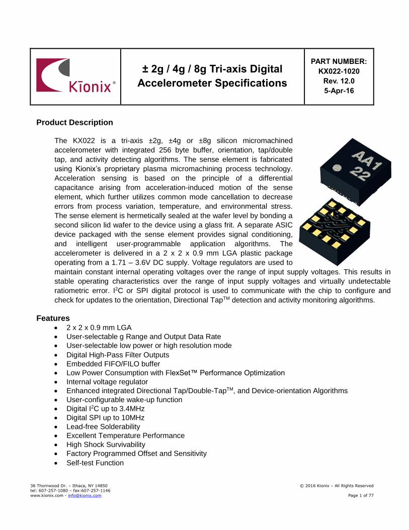
± 2g / 4g / 8g Tri-axis Digital
Accelerometer Specifications
PART NUMBER:
KX022-1020
Rev. 12.0
5-Apr-16
36 Thornwood Dr. – Ithaca, NY 14850 © 2016 Kionix – All Rights Reserved tel: 607-257-1080 – fax:607-257-1146
www.kionix.com - [email protected] Page 1 of 77
Product Description
The KX022 is a tri-axis ±2g, ±4g or ±8g silicon micromachined
accelerometer with integrated 256 byte buffer, orientation, tap/double
tap, and activity detecting algorithms. The sense element is fabricated
using Kionix’s proprietary plasma micromachining process technology.
Acceleration sensing is based on the principle of a differential
capacitance arising from acceleration-induced motion of the sense
element, which further utilizes common mode cancellation to decrease
errors from process variation, temperature, and environmental stress.
The sense element is hermetically sealed at the wafer level by bonding a
second silicon lid wafer to the device using a glass frit. A separate ASIC
device packaged with the sense element provides signal conditioning,
and intelligent user-programmable application algorithms. The
accelerometer is delivered in a 2 x 2 x 0.9 mm LGA plastic package
operating from a 1.71 – 3.6V DC supply. Voltage regulators are used to
maintain constant internal operating voltages over the range of input supply voltages. This results in
stable operating characteristics over the range of input supply voltages and virtually undetectable
ratiometric error. I2C or SPI digital protocol is used to communicate with the chip to configure and
check for updates to the orientation, Directional TapTM detection and activity monitoring algorithms.
Features 2 x 2 x 0.9 mm LGA
User-selectable g Range and Output Data Rate
User-selectable low power or high resolution mode
Digital High-Pass Filter Outputs
Embedded FIFO/FILO buffer
Low Power Consumption with FlexSet™ Performance Optimization
Internal voltage regulator
Enhanced integrated Directional Tap/Double-TapTM, and Device-orientation Algorithms
User-configurable wake-up function
Digital I2C up to 3.4MHz
Digital SPI up to 10MHz
Lead-free Solderability
Excellent Temperature Performance
High Shock Survivability
Factory Programmed Offset and Sensitivity
Self-test Function
± 2g / 4g / 8g Tri-axis Digital
Accelerometer Specifications
PART NUMBER:
KX022-1020
Rev. 12.0
5-Apr-16
36 Thornwood Dr. – Ithaca, NY 14850 © 2016 Kionix – All Rights Reserved tel: 607-257-1080 – fax:607-257-1146
www.kionix.com - [email protected] Page 2 of 77
Table of Contents
PRODUCT DESCRIPTION .................................................................................................................................................................... 1
FEATURES ......................................................................................................................................................................................... 1
TABLE OF CONTENTS ......................................................................................................................................................................... 2
FUNCTIONAL DIAGRAM .................................................................................................................................................................... 6
PRODUCT SPECIFICATIONS ................................................................................................................................................................ 7
MECHANICAL ............................................................................................................................................................................................ 7 ELECTRICAL ............................................................................................................................................................................................... 8
Start Up Time Profile ........................................................................................................................................................................ 9 Current Profile .................................................................................................................................................................................. 9 Power-On Procedure ....................................................................................................................................................................... 10
ENVIRONMENTAL ..................................................................................................................................................................................... 11 TERMINOLOGY ........................................................................................................................................................................................ 12
g ...................................................................................................................................................................................................... 12 Sensitivity ........................................................................................................................................................................................ 12 Zero-g offset ................................................................................................................................................................................... 12 Self-test ........................................................................................................................................................................................... 12
FUNCTIONALITY ....................................................................................................................................................................................... 13 Sense element ................................................................................................................................................................................. 13 ASIC interface ................................................................................................................................................................................. 13 Factory calibration .......................................................................................................................................................................... 13
APPLICATION SCHEMATIC .......................................................................................................................................................................... 14 PIN DESCRIPTIONS ................................................................................................................................................................................... 14 TEST SPECIFICATIONS ................................................................................................................................................................................ 15 PACKAGE DIMENSIONS AND ORIENTATION .................................................................................................................................................... 16
Dimensions ..................................................................................................................................................................................... 16 Orientation ..................................................................................................................................................................................... 17
DIGITAL INTERFACE ......................................................................................................................................................................... 19
I2C SERIAL INTERFACE ............................................................................................................................................................................... 19 I2C Operation .................................................................................................................................................................................. 20 Writing to 8-bit Register ................................................................................................................................................................. 21 Reading from 8-bit Register ............................................................................................................................................................ 21 Data Transfer Sequences ................................................................................................................................................................ 22 HS-mode ......................................................................................................................................................................................... 23 I2C Timing Diagram ......................................................................................................................................................................... 24
SPI COMMUNICATIONS ............................................................................................................................................................................. 25 4-Wire SPI Interface ........................................................................................................................................................................ 25 4-Wire SPI Timing Diagram ............................................................................................................................................................ 26 4-Wire Read and Write Registers ................................................................................................................................................... 27 3-Wire SPI Interface ........................................................................................................................................................................ 28
± 2g / 4g / 8g Tri-axis Digital
Accelerometer Specifications
PART NUMBER:
KX022-1020
Rev. 12.0
5-Apr-16
36 Thornwood Dr. – Ithaca, NY 14850 © 2016 Kionix – All Rights Reserved tel: 607-257-1080 – fax:607-257-1146
www.kionix.com - [email protected] Page 3 of 77
3-Wire SPI Timing Diagram ............................................................................................................................................................ 29 3-Wire Read and Write Registers ................................................................................................................................................... 30
EMBEDDED REGISTERS.................................................................................................................................................................... 31
ACCELEROMETER OUTPUTS ........................................................................................................................................................................ 32 XHP_L .................................................................................................................................................................................................. 33 XHP_H ................................................................................................................................................................................................. 33 YHP_L .................................................................................................................................................................................................. 33 YHP_H ................................................................................................................................................................................................. 33 ZHP_L .................................................................................................................................................................................................. 34 ZHP_H ................................................................................................................................................................................................. 34 XOUT_L ............................................................................................................................................................................................... 34 XOUT_H ............................................................................................................................................................................................... 34 YOUT_L ................................................................................................................................................................................................ 35 YOUT_H ............................................................................................................................................................................................... 35 ZOUT_L ................................................................................................................................................................................................ 35 ZOUT_H ............................................................................................................................................................................................... 35 COTR ................................................................................................................................................................................................... 36 WHO_AM_I ......................................................................................................................................................................................... 36 TSCP .................................................................................................................................................................................................... 36 TSPP .................................................................................................................................................................................................... 37 INS1 ..................................................................................................................................................................................................... 37 INS2 ..................................................................................................................................................................................................... 38 INS3 ..................................................................................................................................................................................................... 39 STATUS_REG ....................................................................................................................................................................................... 39 INT_REL ............................................................................................................................................................................................... 39 CNTL1 .................................................................................................................................................................................................. 40 CNTL2 .................................................................................................................................................................................................. 41 CNTL3 .................................................................................................................................................................................................. 42 ODCNTL ............................................................................................................................................................................................... 44 INC1 ..................................................................................................................................................................................................... 45 INC2 ..................................................................................................................................................................................................... 45 INC3 ..................................................................................................................................................................................................... 46 INC4 ..................................................................................................................................................................................................... 46 INC5 ..................................................................................................................................................................................................... 47 INC6 ..................................................................................................................................................................................................... 47 TILT_TIMER ......................................................................................................................................................................................... 48 WUFC .................................................................................................................................................................................................. 48 TDTRC .................................................................................................................................................................................................. 48 TDTC .................................................................................................................................................................................................... 49 TTH ...................................................................................................................................................................................................... 49 TTL ....................................................................................................................................................................................................... 50 FTD ...................................................................................................................................................................................................... 50 STD ...................................................................................................................................................................................................... 50
± 2g / 4g / 8g Tri-axis Digital
Accelerometer Specifications
PART NUMBER:
KX022-1020
Rev. 12.0
5-Apr-16
36 Thornwood Dr. – Ithaca, NY 14850 © 2016 Kionix – All Rights Reserved tel: 607-257-1080 – fax:607-257-1146
www.kionix.com - [email protected] Page 4 of 77
TLT ....................................................................................................................................................................................................... 51 TWS ..................................................................................................................................................................................................... 51 ATH...................................................................................................................................................................................................... 52 TILT_ANGLE_LL ................................................................................................................................................................................... 52 TILT_ANGLE_HL ................................................................................................................................................................................... 52 HYST_SET ............................................................................................................................................................................................ 53 LP_CNTL .............................................................................................................................................................................................. 53 BUF_CNTL1 ......................................................................................................................................................................................... 54 BUF_CNTL2 ......................................................................................................................................................................................... 55 BUF_STATUS_1 ................................................................................................................................................................................... 56 BUF_STATUS_2 ................................................................................................................................................................................... 56 BUF_CLEAR .......................................................................................................................................................................................... 56 BUF_READ ........................................................................................................................................................................................... 57 SELF_TEST ........................................................................................................................................................................................... 57
EMBEDDED APPLICATIONS ............................................................................................................................................................. 58
ORIENTATION DETECTION FEATURE ............................................................................................................................................................. 58 Hysteresis........................................................................................................................................................................................ 58 Device Orientation Angle (aka Tilt Angle)....................................................................................................................................... 59 Tilt Timer ......................................................................................................................................................................................... 60
MOTION INTERRUPT FEATURE DESCRIPTION ................................................................................................................................................. 61 DIRECTIONAL TAP DETECTION FEATURE DESCRIPTION ..................................................................................................................................... 63
Performance Index.......................................................................................................................................................................... 63 Single Tap Detection ....................................................................................................................................................................... 64 Double Tap Detection ..................................................................................................................................................................... 65
SAMPLE BUFFER FEATURE DESCRIPTION ....................................................................................................................................................... 66 FIFO Mode ...................................................................................................................................................................................... 66 Stream Mode .................................................................................................................................................................................. 66 Trigger Mode .................................................................................................................................................................................. 67 FILO Mode ...................................................................................................................................................................................... 67 Buffer Operation ............................................................................................................................................................................. 67
REVISION HISTORY .......................................................................................................................................................................... 73
NOTICE............................................................................................................................................................................................ 75
PRECAUTION ON USING KIONIX PRODUCTS .................................................................................................................................................. 75 PRECAUTION FOR MOUNTING / CIRCUIT BOARD DESIGN .................................................................................................................................. 76 PRECAUTIONS REGARDING APPLICATION EXAMPLES AND EXTERNAL CIRCUITS ..................................................................................................... 76 PRECAUTION FOR ELECTROSTATIC ............................................................................................................................................................... 76 PRECAUTION FOR STORAGE / TRANSPORTATION ............................................................................................................................................ 76 PRECAUTION FOR PRODUCT LABEL .............................................................................................................................................................. 77 PRECAUTION FOR DISPOSITION ................................................................................................................................................................... 77 PRECAUTION FOR FOREIGN EXCHANGE AND FOREIGN TRADE ACT ...................................................................................................................... 77 PRECAUTION REGARDING INTELLECTUAL PROPERTY RIGHTS ............................................................................................................................. 77 OTHER PRECAUTION ................................................................................................................................................................................. 77
± 2g / 4g / 8g Tri-axis Digital
Accelerometer Specifications
PART NUMBER:
KX022-1020
Rev. 12.0
5-Apr-16
36 Thornwood Dr. – Ithaca, NY 14850 © 2016 Kionix – All Rights Reserved tel: 607-257-1080 – fax:607-257-1146
www.kionix.com - [email protected] Page 5 of 77
GENERAL PRECAUTION .............................................................................................................................................................................. 77
± 2g / 4g / 8g Tri-axis Digital
Accelerometer Specifications
PART NUMBER:
KX022-1020
Rev. 12.0
5-Apr-16
36 Thornwood Dr. – Ithaca, NY 14850 © 2016 Kionix – All Rights Reserved tel: 607-257-1080 – fax:607-257-1146
www.kionix.com - [email protected] Page 6 of 77
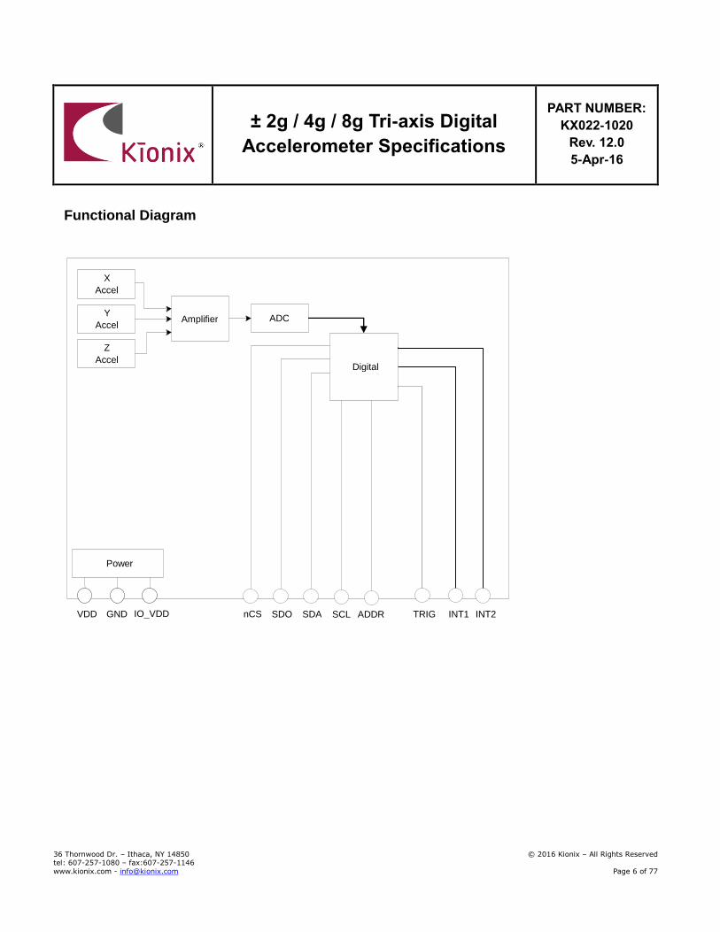
Functional Diagram
Z Accel
Y Accel
ADC
Digital
Power
X Accel
Amplifier
VDD GND IO_VDD SDA SCL ADDR INT1 TRIG SDO nCS INT2
± 2g / 4g / 8g Tri-axis Digital
Accelerometer Specifications
PART NUMBER:
KX022-1020
Rev. 12.0
5-Apr-16
36 Thornwood Dr. – Ithaca, NY 14850 © 2016 Kionix – All Rights Reserved tel: 607-257-1080 – fax:607-257-1146
www.kionix.com - [email protected] Page 7 of 77
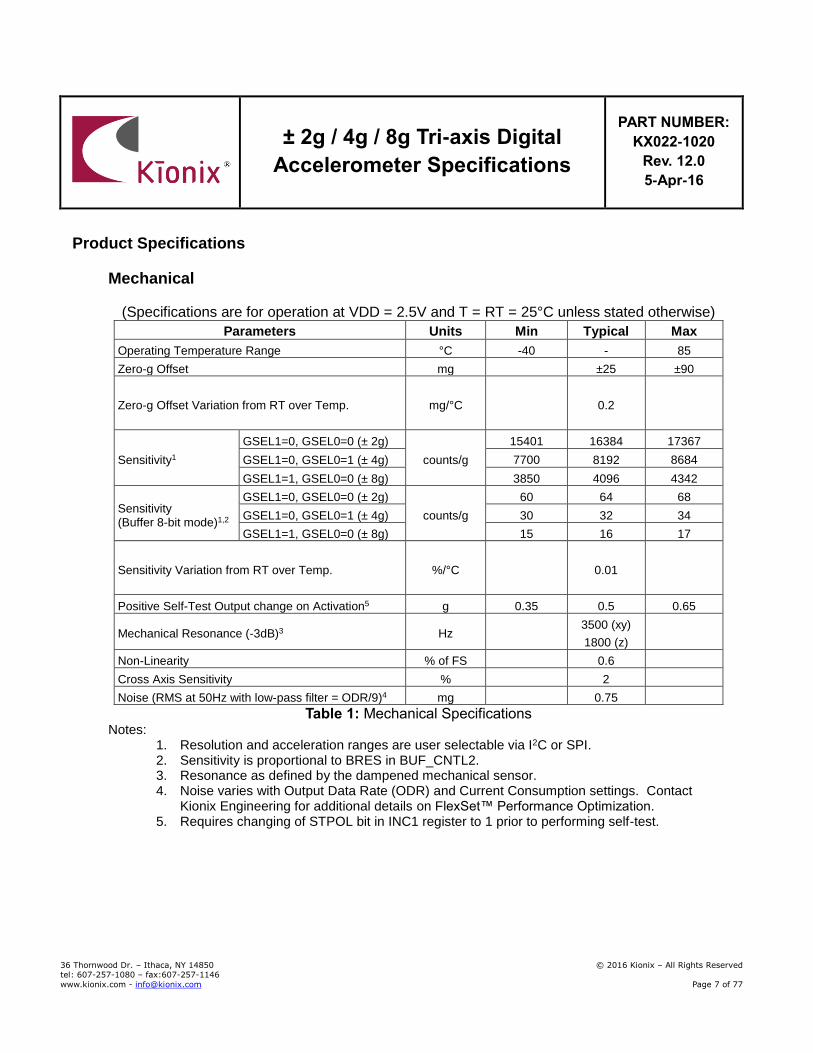
Product Specifications
Mechanical
(Specifications are for operation at VDD = 2.5V and T = RT = 25°C unless stated otherwise)
Parameters Units Min Typical Max
Operating Temperature Range °C -40 - 85
Zero-g Offset mg ±25 ±90
Zero-g Offset Variation from RT over Temp. mg/°C
0.2
Sensitivity1
GSEL1=0, GSEL0=0 (± 2g)
counts/g
15401 16384 17367
GSEL1=0, GSEL0=1 (± 4g) 7700 8192 8684
GSEL1=1, GSEL0=0 (± 8g) 3850 4096 4342
Sensitivity (Buffer 8-bit mode)1,2
GSEL1=0, GSEL0=0 (± 2g)
counts/g
60 64 68
GSEL1=0, GSEL0=1 (± 4g) 30 32 34
GSEL1=1, GSEL0=0 (± 8g) 15 16 17
Sensitivity Variation from RT over Temp. %/°C
0.01
Positive Self-Test Output change on Activation5 g 0.35 0.5 0.65
Mechanical Resonance (-3dB)3 Hz
3500 (xy)
1800 (z)
Non-Linearity % of FS 0.6
Cross Axis Sensitivity % 2
Noise (RMS at 50Hz with low-pass filter = ODR/9)4 mg 0.75
Table 1: Mechanical Specifications Notes:
1. Resolution and acceleration ranges are user selectable via I2C or SPI. 2. Sensitivity is proportional to BRES in BUF_CNTL2. 3. Resonance as defined by the dampened mechanical sensor. 4. Noise varies with Output Data Rate (ODR) and Current Consumption settings. Contact
Kionix Engineering for additional details on FlexSet™ Performance Optimization. 5. Requires changing of STPOL bit in INC1 register to 1 prior to performing self-test.
± 2g / 4g / 8g Tri-axis Digital
Accelerometer Specifications
PART NUMBER:
KX022-1020
Rev. 12.0
5-Apr-16
36 Thornwood Dr. – Ithaca, NY 14850 © 2016 Kionix – All Rights Reserved tel: 607-257-1080 – fax:607-257-1146
www.kionix.com - [email protected] Page 8 of 77
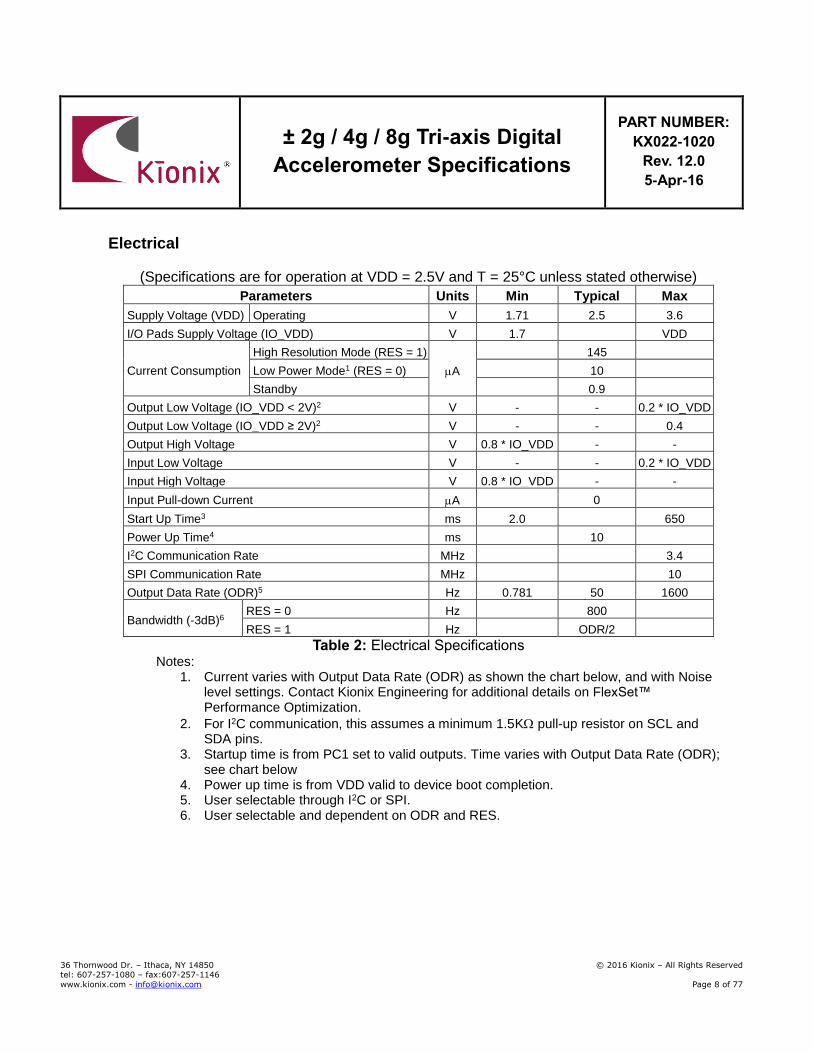
Electrical
(Specifications are for operation at VDD = 2.5V and T = 25°C unless stated otherwise)
Parameters Units Min Typical Max
Supply Voltage (VDD) Operating V 1.71 2.5 3.6
I/O Pads Supply Voltage (IO_VDD) V 1.7 VDD
Current Consumption
High Resolution Mode (RES = 1)
A
145
Low Power Mode1 (RES = 0) 10
Standby 0.9
Output Low Voltage (IO_VDD < 2V)2 V - - 0.2 * IO_VDD
Output Low Voltage (IO_VDD ≥ 2V)2 V - - 0.4
Output High Voltage V 0.8 * IO_VDD - -
Input Low Voltage V - - 0.2 * IO_VDD
Input High Voltage V 0.8 * IO_VDD - -
Input Pull-down Current A 0
Start Up Time3 ms 2.0 650
Power Up Time4 ms 10
I2C Communication Rate MHz 3.4
SPI Communication Rate MHz 10
Output Data Rate (ODR)5 Hz 0.781 50 1600
Bandwidth (-3dB)6 RES = 0 Hz 800
RES = 1 Hz ODR/2
Table 2: Electrical Specifications
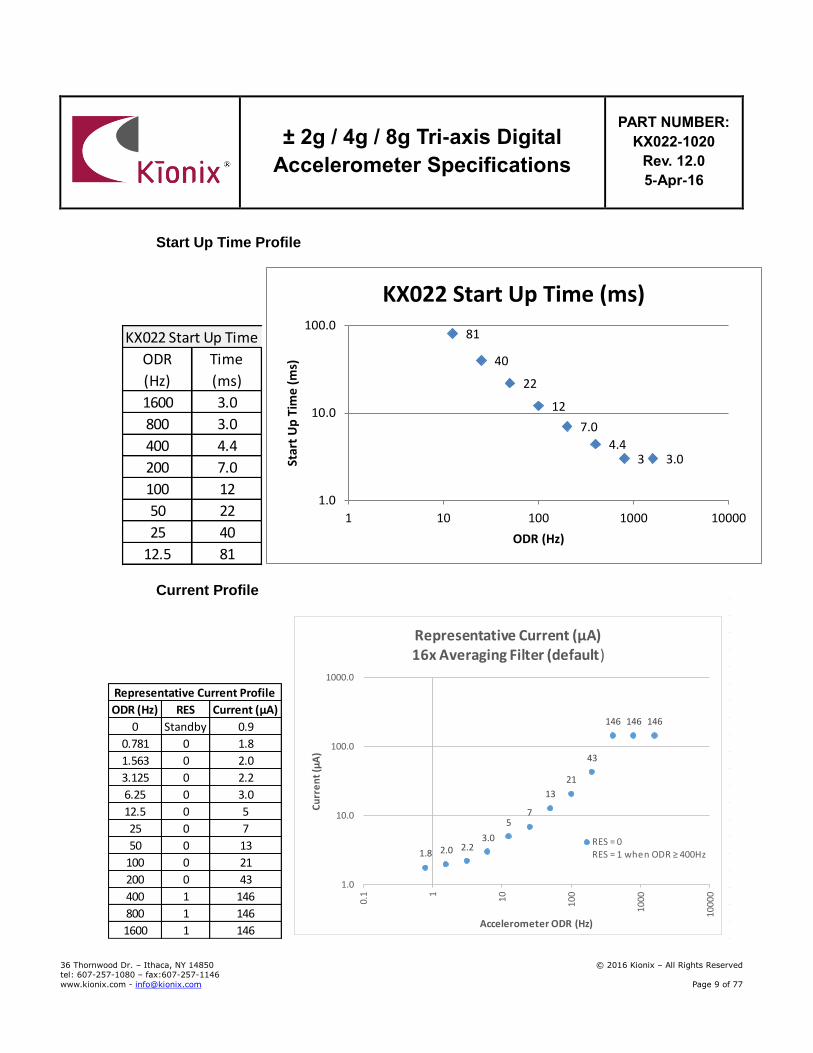
Notes: 1. Current varies with Output Data Rate (ODR) as shown the chart below, and with Noise
level settings. Contact Kionix Engineering for additional details on FlexSet™ Performance Optimization.
2. For I2C communication, this assumes a minimum 1.5K pull-up resistor on SCL and SDA pins.
3. Startup time is from PC1 set to valid outputs. Time varies with Output Data Rate (ODR); see chart below
4. Power up time is from VDD valid to device boot completion. 5. User selectable through I2C or SPI. 6. User selectable and dependent on ODR and RES.
± 2g / 4g / 8g Tri-axis Digital
Accelerometer Specifications
PART NUMBER:
KX022-1020
Rev. 12.0
5-Apr-16
36 Thornwood Dr. – Ithaca, NY 14850 © 2016 Kionix – All Rights Reserved tel: 607-257-1080 – fax:607-257-1146
www.kionix.com - [email protected] Page 9 of 77
Start Up Time Profile
Current Profile
ODR
(Hz)
Time
(ms)
1600 3.0
800 3.0
400 4.4
200 7.0
100 12
50 22
25 40
12.5 81
KX022 Start Up Time
3.034.4
7.0
12
22
40
81
1.0
10.0
100.0
1 10 100 1000 10000
Star
t U
p T
ime
(m
s)
ODR (Hz)
KX022 Start Up Time (ms)
ODR (Hz) RES Current (µA)
0 Standby 0.9
0.781 0 1.8
1.563 0 2.0
3.125 0 2.2
6.25 0 3.0
12.5 0 5
25 0 7
50 0 13
100 0 21
200 0 43
400 1 146
800 1 146
1600 1 146
Representative Current Profile
1.8 2.0 2.23.0
57
13
21
43
146 146 146
1.0
10.0
100.0
1000.0
0.1 1
10
100
1000
10
00
0
Cu
rre
nt
(µA
)
Accelerometer ODR (Hz)
Representative Current (µA)16x Averaging Filter (default)
RES = 0
RES = 1 when ODR ≥ 400Hz
± 2g / 4g / 8g Tri-axis Digital
Accelerometer Specifications
PART NUMBER:
KX022-1020
Rev. 12.0
5-Apr-16
36 Thornwood Dr. – Ithaca, NY 14850 © 2016 Kionix – All Rights Reserved tel: 607-257-1080 – fax:607-257-1146
www.kionix.com - [email protected] Page 10 of 77
Power-On Procedure
Proper functioning of power-on reset (POR) is dependent on the specific VDD, VDDLow, TVDD (rise time), and TVDD_Off profile of individual applications. It is recommended to minimize VDDLow, and TVDD, and maximize TVDD_Off. It is also advised that the VDD ramp up time TVDD be monotonic. Note that the outputs will not be stable until VDD has reached its final value.
To assure proper POR, the application should be evaluated over the customer specified range of VDD, VDDLow, TVDD, TVDD_Off and temperature as POR performance can vary depending on these parameters.
Please refer to Technical Note TN014 KX022, KX023 Accelerometer Power-On Procedure for more information.

± 2g / 4g / 8g Tri-axis Digital
Accelerometer Specifications
PART NUMBER:
KX022-1020
Rev. 12.0
5-Apr-16
36 Thornwood Dr. – Ithaca, NY 14850 © 2016 Kionix – All Rights Reserved tel: 607-257-1080 – fax:607-257-1146
www.kionix.com - [email protected] Page 11 of 77
HF
Environmental
Parameters Units Min Typical Max
Supply Voltage (VDD) Absolute Limits V -0.5 - 3.63
Operating Temperature Range °C -40 - 85
Storage Temperature Range °C -55 - 150
Mech. Shock (powered and unpowered) g - - 5000 for 0.5ms
10000 for 0.2ms
ESD HBM V - - 2000
Table 3: Environmental Specifications
Caution: ESD Sensitive and Mechanical Shock Sensitive Component, improper handling can cause permanent damage to the device.
These products conform to RoHS Directive 2011/65/EU of the European Parliament and of the Council of the European Union that was issued June 8, 2011. Specifically, these products do not contain any non-exempted amounts of lead, mercury, cadmium, hexavalent chromium, polybrominated biphenyls (PBB) or polybrominated diphenyl ethers (PBDE)
above the maximum concentration values (MCV) by weight in any of its homogenous materials. Homogenous materials are “of uniform composition throughout”. The MCV for lead, mercury, hexavalent chromium, PBB, and PBDE is 0.10%. The MCV for cadmium is 0.010%. Applicable Exemption: 7C-I - Electrical and electronic components containing lead in a glass or ceramic other than dielectric ceramic in capacitors (piezoelectronic devices) or in a glass or ceramic matrix compound.
These products are also in conformance with REACH Regulation No 1907/2006 of the European Parliament and of the Council that was issued Dec. 30, 2011. They do not contain any Substances of Very High Concern (SVHC-161) as identified by the European Chemicals Agency as of 17 December 2014.
This product is halogen-free per IEC 61249-2-21. Specifically, the materials used in this product contain a maximum total halogen content of 1500 ppm with less than 900-ppm bromine and less than 900-ppm chlorine.
Soldering
Soldering recommendations are available upon request or from www.kionix.com.
± 2g / 4g / 8g Tri-axis Digital
Accelerometer Specifications
PART NUMBER:
KX022-1020
Rev. 12.0
5-Apr-16
36 Thornwood Dr. – Ithaca, NY 14850 © 2016 Kionix – All Rights Reserved tel: 607-257-1080 – fax:607-257-1146
www.kionix.com - [email protected] Page 12 of 77
Terminology
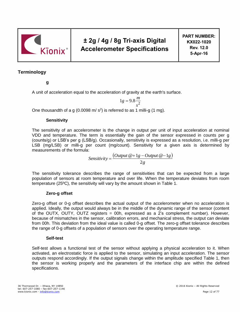
g A unit of acceleration equal to the acceleration of gravity at the earth's surface.
28.91
s
mg
One thousandth of a g (0.0098 m/ s2) is referred to as 1 milli-g (1 mg).
Sensitivity The sensitivity of an accelerometer is the change in output per unit of input acceleration at nominal VDD and temperature. The term is essentially the gain of the sensor expressed in counts per g (counts/g) or LSB’s per g (LSB/g). Occasionally, sensitivity is expressed as a resolution, i.e. milli-g per LSB (mg/LSB) or milli-g per count (mg/count). Sensitivity for a given axis is determined by measurements of the formula:
g
gOutputgOutputySensitivit
2
1@1@
The sensitivity tolerance describes the range of sensitivities that can be expected from a large population of sensors at room temperature and over life. When the temperature deviates from room temperature (25ºC), the sensitivity will vary by the amount shown in Table 1.
Zero-g offset Zero-g offset or 0-g offset describes the actual output of the accelerometer when no acceleration is applied. Ideally, the output would always be in the middle of the dynamic range of the sensor (content of the OUTX, OUTY, OUTZ registers = 00h, expressed as a 2’s complement number). However, because of mismatches in the sensor, calibration errors, and mechanical stress, the output can deviate from 00h. This deviation from the ideal value is called 0-g offset. The zero-g offset tolerance describes the range of 0-g offsets of a population of sensors over the operating temperature range.
Self-test Self-test allows a functional test of the sensor without applying a physical acceleration to it. When activated, an electrostatic force is applied to the sensor, simulating an input acceleration. The sensor outputs respond accordingly. If the output signals change within the amplitude specified Table 1, then the sensor is working properly and the parameters of the interface chip are within the defined specifications.
± 2g / 4g / 8g Tri-axis Digital
Accelerometer Specifications
PART NUMBER:
KX022-1020
Rev. 12.0
5-Apr-16
36 Thornwood Dr. – Ithaca, NY 14850 © 2016 Kionix – All Rights Reserved tel: 607-257-1080 – fax:607-257-1146
www.kionix.com - [email protected] Page 13 of 77
Functionality
Sense element The sense element is fabricated using Kionix’s proprietary plasma micromachining process technology. This process technology allows Kionix to create mechanical silicon structures which are essentially mass-spring systems that move in the direction of the applied acceleration. Acceleration sensing is based on the principle of a differential capacitance arising from the acceleration-induced motion. Capacitive plates on the moving mass move relative to fixed capacitive plates anchored to the substrate. The sense element is hermetically sealed at the wafer level by bonding a second silicon lid wafer to the device using a glass frit.
ASIC interface A separate ASIC device packaged with the sense element provides all of the signal conditioning and communication with the sensor. The complete measurement chain is composed by a low-noise capacitance to voltage amplifier which converts the differential capacitance of the MEMS sensor into an analog voltage that is sent through an analog-to-digital converter. The acceleration data may be accessed through the I2C digital communications provided by the ASIC. In addition, the ASIC contains all of the logic to allow the user to choose data rates, g-ranges, filter settings, and interrupt logic. Plus, there are two programmable state machines which allow the user to create unique embedded functions based on changes in acceleration.
Factory calibration Kionix trims the offset and sensitivity of each accelerometer by adjusting gain (sensitivity) and 0-g offset trim codes stored in nonvolatile memory (OTP). Additionally, all functional register default values are also programmed into the nonvolatile memory. Every time the device is turned on or a software reset command is issued, the trimming parameters and default register values are downloaded into the volatile registers to be used during active operation. This allows the device to function without further calibration.
± 2g / 4g / 8g Tri-axis Digital
Accelerometer Specifications
PART NUMBER:
KX022-1020
Rev. 12.0
5-Apr-16
36 Thornwood Dr. – Ithaca, NY 14850 © 2016 Kionix – All Rights Reserved tel: 607-257-1080 – fax:607-257-1146
www.kionix.com - [email protected] Page 14 of 77
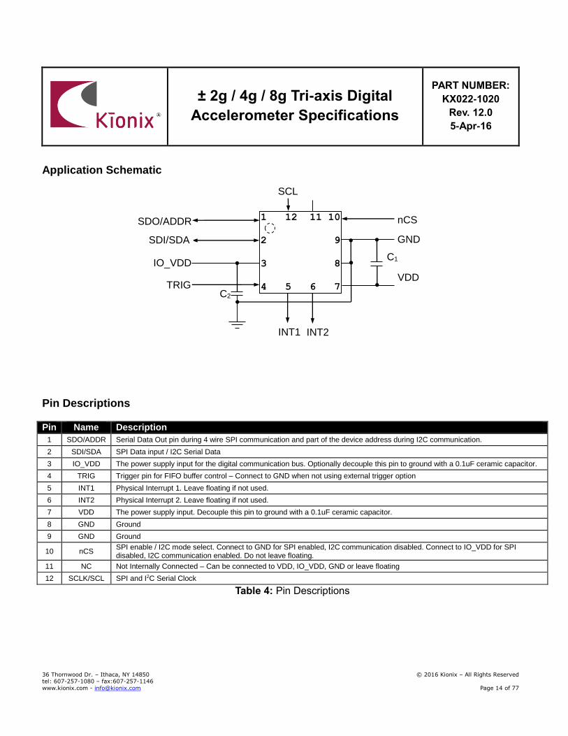
Application Schematic
Pin Descriptions Pin Name Description
1 SDO/ADDR Serial Data Out pin during 4 wire SPI communication and part of the device address during I2C communication.
2 SDI/SDA SPI Data input / I2C Serial Data
3 IO_VDD The power supply input for the digital communication bus. Optionally decouple this pin to ground with a 0.1uF ceramic capacitor.
4 TRIG Trigger pin for FIFO buffer control – Connect to GND when not using external trigger option
5 INT1 Physical Interrupt 1. Leave floating if not used.
6 INT2 Physical Interrupt 2. Leave floating if not used.
7 VDD The power supply input. Decouple this pin to ground with a 0.1uF ceramic capacitor.
8 GND Ground
9 GND Ground
10 nCS SPI enable / I2C mode select. Connect to GND for SPI enabled, I2C communication disabled. Connect to IO_VDD for SPI disabled, I2C communication enabled. Do not leave floating.
11 NC Not Internally Connected – Can be connected to VDD, IO_VDD, GND or leave floating
12 SCLK/SCL SPI and I2C Serial Clock
Table 4: Pin Descriptions
1 12 11 10
2 9
3 8
4 5 6 7
SDO/ADDR
SDI/SDA
IO_VDD
TRIG
INT1 INT2
VDD
GND
nCS
SCL
C1
C2
± 2g / 4g / 8g Tri-axis Digital
Accelerometer Specifications
PART NUMBER:
KX022-1020
Rev. 12.0
5-Apr-16
36 Thornwood Dr. – Ithaca, NY 14850 © 2016 Kionix – All Rights Reserved tel: 607-257-1080 – fax:607-257-1146
www.kionix.com - [email protected] Page 15 of 77
Test Specifications
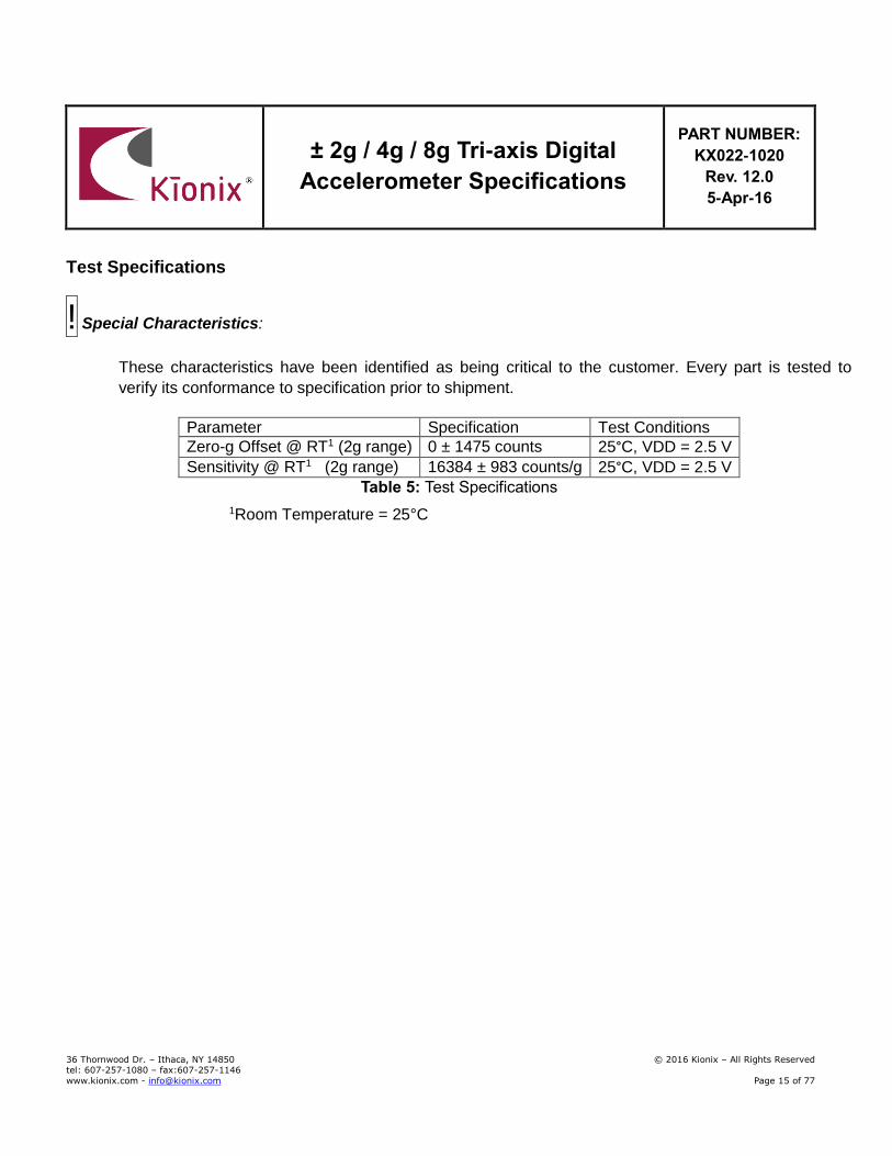
! Special Characteristics:
These characteristics have been identified as being critical to the customer. Every part is tested to
verify its conformance to specification prior to shipment.
Parameter Specification Test Conditions
Zero-g Offset @ RT1 (2g range) 0 ± 1475 counts 25°C, VDD = 2.5 V
Sensitivity @ RT1 (2g range) 16384 ± 983 counts/g 25°C, VDD = 2.5 V
Table 5: Test Specifications
1Room Temperature = 25°C
± 2g / 4g / 8g Tri-axis Digital
Accelerometer Specifications
PART NUMBER:
KX022-1020
Rev. 12.0
5-Apr-16
36 Thornwood Dr. – Ithaca, NY 14850 © 2016 Kionix – All Rights Reserved tel: 607-257-1080 – fax:607-257-1146
www.kionix.com - [email protected] Page 16 of 77
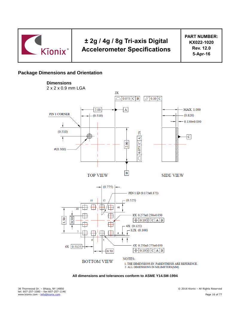
Package Dimensions and Orientation
Dimensions 2 x 2 x 0.9 mm LGA
All dimensions and tolerances conform to ASME Y14.5M-1994
± 2g / 4g / 8g Tri-axis Digital
Accelerometer Specifications
PART NUMBER:
KX022-1020
Rev. 12.0
5-Apr-16
36 Thornwood Dr. – Ithaca, NY 14850 © 2016 Kionix – All Rights Reserved tel: 607-257-1080 – fax:607-257-1146
www.kionix.com - [email protected] Page 17 of 77
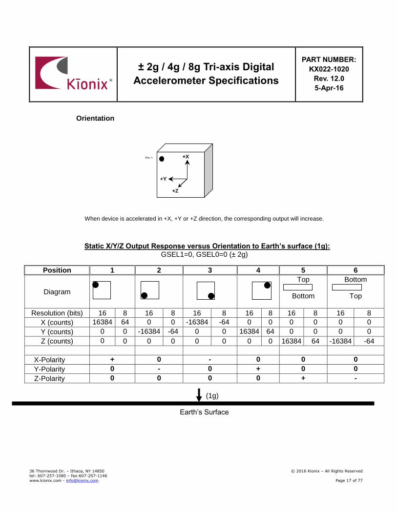
Orientation
When device is accelerated in +X, +Y or +Z direction, the corresponding output will increase.
Static X/Y/Z Output Response versus Orientation to Earth’s surface (1g): GSEL1=0, GSEL0=0 (± 2g)
Position 1 2 3 4 5 6
Diagram
Top
Bottom
Bottom
Top
Resolution (bits) 16 8 16 8 16 8 16 8 16 8 16 8
X (counts) 16384
64
0
0
-16384
-64
0
0
0
0
0
0 Y (counts) 0
0
-16384 0
-64
0
0
16384
64
0
0
0
0 Z (counts) 0
0
0 0 0 0 0 0 0 16384 64 -16384 -64
X-Polarity + 0 - 0 0 0
Y-Polarity 0 - 0 + 0 0
Z-Polarity 0 0 0 0 + -
(1g)
Earth’s Surface
Pin 1 +X
+Y
+Z
± 2g / 4g / 8g Tri-axis Digital
Accelerometer Specifications
PART NUMBER:
KX022-1020
Rev. 12.0
5-Apr-16
36 Thornwood Dr. – Ithaca, NY 14850 © 2016 Kionix – All Rights Reserved tel: 607-257-1080 – fax:607-257-1146
www.kionix.com - [email protected] Page 18 of 77
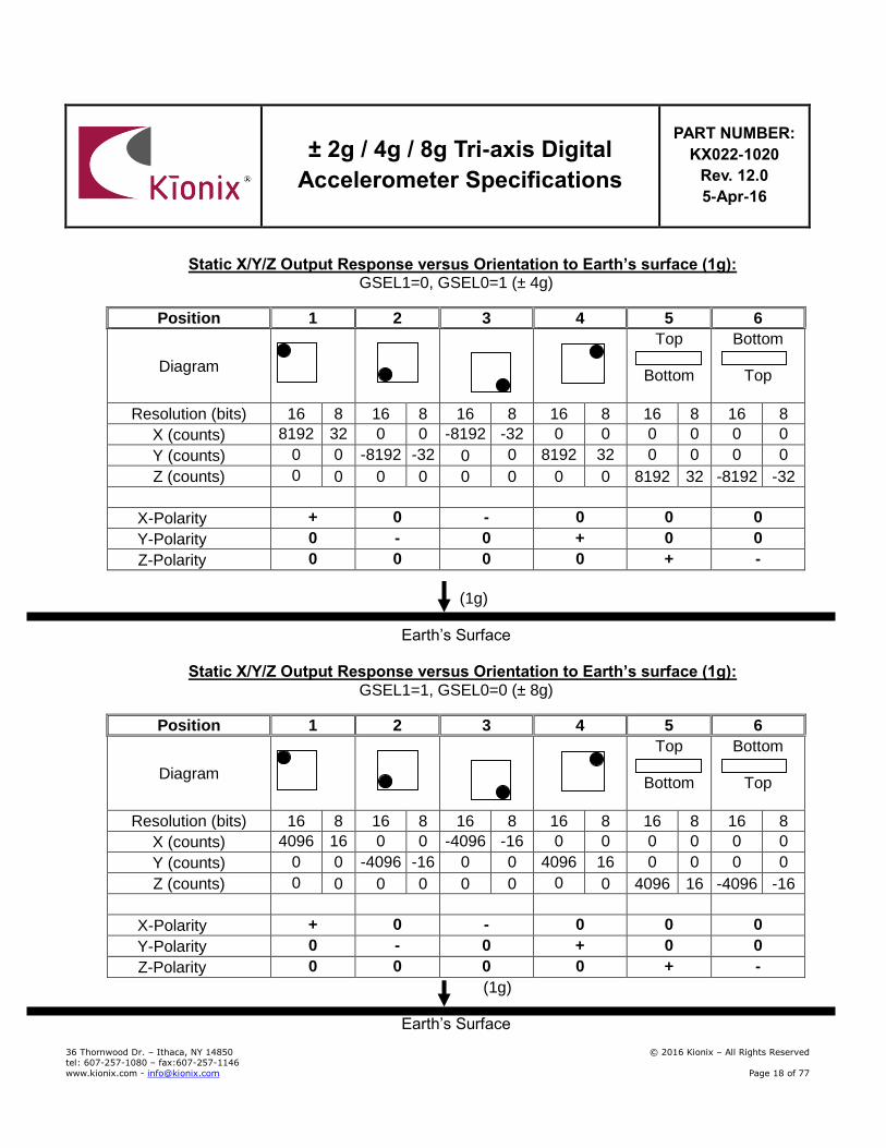
Static X/Y/Z Output Response versus Orientation to Earth’s surface (1g): GSEL1=0, GSEL0=1 (± 4g)
Position 1 2 3 4 5 6
Diagram
Top
Bottom
Bottom
Top
Resolution (bits) 16 8 16 8 16 8 16 8 16 8 16 8
X (counts) 8192
32
0
0
-8192
-32
0
0
0
0
0
0 Y (counts) 0
0
-8192
-32
0 0
8192
32
0
0
0
0 Z (counts) 0
0
0 0 0 0 0 0 0 8192 32 -8192 -32
X-Polarity + 0 - 0 0 0
Y-Polarity 0 - 0 + 0 0
Z-Polarity 0 0 0 0 + -
(1g)
Earth’s Surface
Static X/Y/Z Output Response versus Orientation to Earth’s surface (1g):
GSEL1=1, GSEL0=0 (± 8g)
Position 1 2 3 4 5 6
Diagram
Top
Bottom
Bottom
Top
Resolution (bits) 16 8 16 8 16 8 16 8 16 8 16 8
X (counts) 4096
16
0
0
-4096
-16
0
0
0
0
0
0 Y (counts) 0
0
-4096
-16
0
0
4096
16
0
0
0
0 Z (counts) 0
0
0 0 0 0 0 0
0 4096 16 -4096 -16
X-Polarity + 0 - 0 0 0
Y-Polarity 0 - 0 + 0 0
Z-Polarity 0 0 0 0 + -
(1g)
Earth’s Surface

± 2g / 4g / 8g Tri-axis Digital
Accelerometer Specifications
PART NUMBER:
KX022-1020
Rev. 12.0
5-Apr-16
36 Thornwood Dr. – Ithaca, NY 14850 © 2016 Kionix – All Rights Reserved tel: 607-257-1080 – fax:607-257-1146
www.kionix.com - [email protected] Page 19 of 77
Digital Interface The Kionix KX022 digital accelerometer has the ability to communicate via the I2C and SPI digital serial interface protocols. This allows for easy system integration by eliminating analog-to-digital converter requirements and by providing direct communication with system micro-controllers. The serial interface terms and descriptions as indicated in Table 6 below will be observed throughout this document.
Term Description
Transmitter The device that transmits data to the bus.
Receiver The device that receives data from the bus.
Master The device that initiates a transfer, generates clock signals, and terminates a transfer.
Slave The device addressed by the Master.
Table 6: Serial Interface Terminologies
I2C Serial Interface As previously mentioned, the KX022 has the ability to communicate on an I2C bus. I2C is primarily used for synchronous serial communication between a Master device and one or more Slave devices. The Master, typically a micro controller, provides the serial clock signal and addresses Slave devices on the bus. The KX022 always operates as a Slave device during standard Master-Slave I2C operation. I2C is a two-wire serial interface that contains a Serial Clock (SCL) line and a Serial Data (SDA) line. SCL is a serial clock that is provided by the Master, but can be held low by any Slave device, putting the Master into a wait condition. SDA is a bi-directional line used to transmit and receive data to and from the interface. Data is transmitted MSB (Most Significant Bit) first in 8-bit per byte format, and the number of bytes transmitted per transfer is unlimited. The I2C bus is considered free when both lines are high. The I2C interface is compliant with high-speed mode, fast mode and standard mode I2C protocols.
± 2g / 4g / 8g Tri-axis Digital
Accelerometer Specifications
PART NUMBER:
KX022-1020
Rev. 12.0
5-Apr-16
36 Thornwood Dr. – Ithaca, NY 14850 © 2016 Kionix – All Rights Reserved tel: 607-257-1080 – fax:607-257-1146
www.kionix.com - [email protected] Page 20 of 77
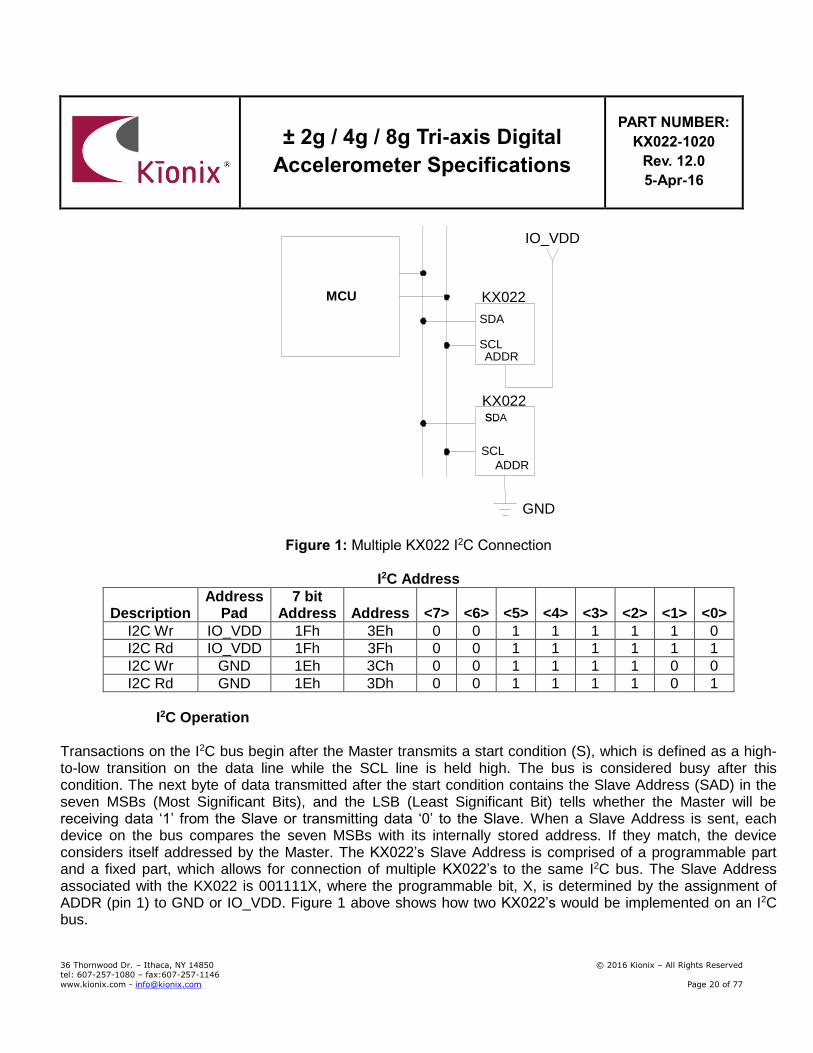
Figure 1: Multiple KX022 I2C Connection
I2C Address
Description Address
Pad 7 bit
Address Address <7> <6> <5> <4> <3> <2> <1> <0>
I2C Wr IO_VDD 1Fh 3Eh 0 0 1 1 1 1 1 0
I2C Rd IO_VDD 1Fh 3Fh 0 0 1 1 1 1 1 1
I2C Wr GND 1Eh 3Ch 0 0 1 1 1 1 0 0
I2C Rd GND 1Eh 3Dh 0 0 1 1 1 1 0 1
I2C Operation
Transactions on the I2C bus begin after the Master transmits a start condition (S), which is defined as a high-to-low transition on the data line while the SCL line is held high. The bus is considered busy after this condition. The next byte of data transmitted after the start condition contains the Slave Address (SAD) in the seven MSBs (Most Significant Bits), and the LSB (Least Significant Bit) tells whether the Master will be receiving data ‘1’ from the Slave or transmitting data ‘0’ to the Slave. When a Slave Address is sent, each device on the bus compares the seven MSBs with its internally stored address. If they match, the device considers itself addressed by the Master. The KX022’s Slave Address is comprised of a programmable part and a fixed part, which allows for connection of multiple KX022’s to the same I2C bus. The Slave Address associated with the KX022 is 001111X, where the programmable bit, X, is determined by the assignment of ADDR (pin 1) to GND or IO_VDD. Figure 1 above shows how two KX022’s would be implemented on an I2C bus.
MCU
KX022
SDA
SCL ADDR
SDA SL
ADDR
SCL
KX022
IO_VDD
GND
± 2g / 4g / 8g Tri-axis Digital
Accelerometer Specifications
PART NUMBER:
KX022-1020
Rev. 12.0
5-Apr-16
36 Thornwood Dr. – Ithaca, NY 14850 © 2016 Kionix – All Rights Reserved tel: 607-257-1080 – fax:607-257-1146
www.kionix.com - [email protected] Page 21 of 77
It is mandatory that receiving devices acknowledge (ACK) each transaction. Therefore, the transmitter must release the SDA line during this ACK pulse. The receiver then pulls the data line low so that it remains stable low during the high period of the ACK clock pulse. A receiver that has been addressed, whether it is Master or Slave, is obliged to generate an ACK after each byte of data has been received. To conclude a transaction, the Master must transmit a stop condition (P) by transitioning the SDA line from low to high while SCL is high. The I2C bus is now free. Note that if the KX022 is accessed through I2C protocol before the startup is finished a NACK signal is sent.
Writing to 8-bit Register Upon power up, the Master must write to the KX022’s control registers to set its operational mode. Therefore, when writing to a control register on the I2C bus, as shown Sequence 1 on the following page, the following protocol must be observed: After a start condition, SAD+W transmission, and the KX022 ACK has been returned, an 8-bit Register Address (RA) command is transmitted by the Master. This command is telling the KX022 to which 8-bit register the Master will be writing the data. Since this is I2C mode, the MSB of the RA command should always be zero (0). The KX022 acknowledges the RA and the Master transmits the data to be stored in the 8-bit register. The KX022 acknowledges that it has received the data and the Master transmits a stop condition (P) to end the data transfer. The data sent to the KX022 is now stored in the appropriate register. The KX022 automatically increments the received RA commands and, therefore, multiple bytes of data can be written to sequential registers after each Slave ACK as shown in Sequence 2 on the following page. Note** If a STOP condition is sent on the least significant bit of write data or the following master acknowledge cycle, the last write operation is not guaranteed and it may alter the content of the affected registers.
Reading from 8-bit Register
When reading data from a KX022 8-bit register on the I2C bus, as shown in Sequence 3 on the next page, the following protocol must be observed: The Master first transmits a start condition (S) and the appropriate Slave Address (SAD) with the LSB set at ‘0’ to write. The KX022 acknowledges and the Master transmits the 8-bit RA of the register it wants to read. The KX022 again acknowledges, and the Master transmits a repeated start condition (Sr). After the repeated start condition, the Master addresses the KX022 with a ‘1’ in the LSB (SAD+R) to read from the previously selected register. The Slave then acknowledges and transmits the data from the requested register. The Master does not acknowledge (NACK) it received the transmitted data, but transmits a stop condition to end the data transfer. Note that the KX022 automatically increments through its sequential registers, allowing data to be read from multiple registers following a single SAD+R command as shown below in Sequence 4 on the following page. Reading data from a buffer read register is a special case because if register address (RA) is set to buffer read register (BUF_READ) in Sequence 4, the register auto-increment feature is automatically disabled. Instead, the Read Pointer will increment to the next data in the buffer, thus allowing reading multiple bytes of data from the buffer using a single SAD+R command. Note** Accelerometer’s output data should be read in a single transaction using the auto-increment feature to prevent output data from being updated prior to intended completion of the read transaction.
± 2g / 4g / 8g Tri-axis Digital
Accelerometer Specifications
PART NUMBER:
KX022-1020
Rev. 12.0
5-Apr-16
36 Thornwood Dr. – Ithaca, NY 14850 © 2016 Kionix – All Rights Reserved tel: 607-257-1080 – fax:607-257-1146
www.kionix.com - [email protected] Page 22 of 77
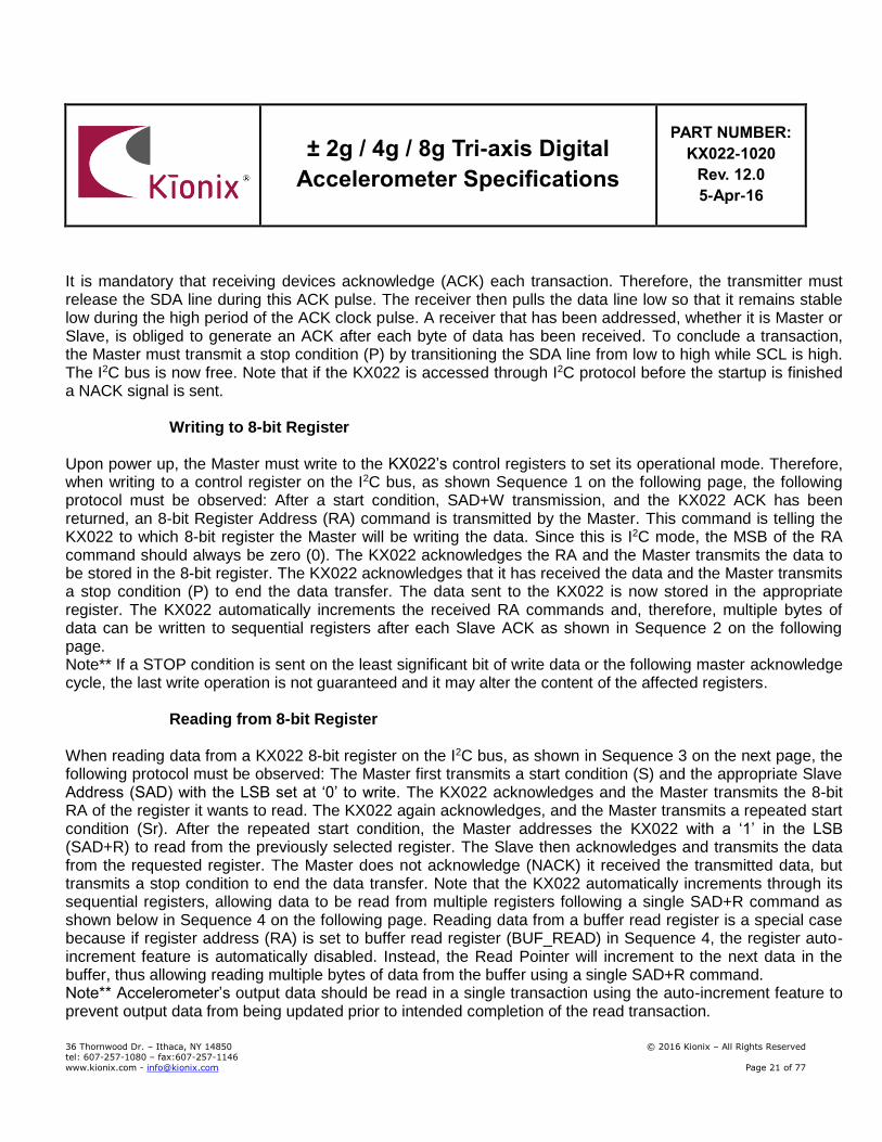
Data Transfer Sequences The following information clearly illustrates the variety of data transfers that can occur on the I2C bus and how the Master and Slave interact during these transfers. Table 7 defines the I2C terms used during the data transfers.
Term Definition
S Start Condition
Sr Repeated Start Condition
SAD Slave Address
W Write Bit
R Read Bit
ACK Acknowledge
NACK Not Acknowledge
RA Register Address
Data Transmitted/Received Data
P Stop Condition
Table 7: I2C Terms
Sequence 1. The Master is writing one byte to the Slave.
Master S SAD + W RA DATA P
Slave ACK ACK ACK
Sequence 2. The Master is writing multiple bytes to the Slave.
Master S SAD + W RA DATA DATA P
Slave ACK ACK ACK ACK
Sequence 3. The Master is receiving one byte of data from the Slave.
Master S SAD + W RA Sr SAD + R NACK P
Slave ACK ACK ACK DATA
Sequence 4. The Master is receiving multiple bytes of data from the Slave.
Master S SAD + W RA Sr SAD + R ACK NACK P
Slave ACK ACK ACK DATA DATA
± 2g / 4g / 8g Tri-axis Digital
Accelerometer Specifications
PART NUMBER:
KX022-1020
Rev. 12.0
5-Apr-16
36 Thornwood Dr. – Ithaca, NY 14850 © 2016 Kionix – All Rights Reserved tel: 607-257-1080 – fax:607-257-1146
www.kionix.com - [email protected] Page 23 of 77
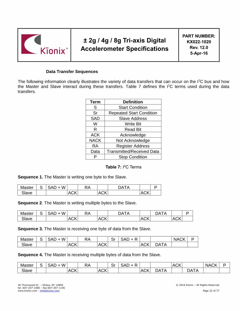
HS-mode To enter the 3.4MHz high speed mode of communication, the device must receive the following sequence of conditions from the master: a Start condition followed by a Master code (00001XXX) and a Master Non-acknowledge. Once recognized, the device switches to HS-mode communication. Read/write data transfers then proceed as described in the sequences above. Devices return to the FS-mode after a STOP occurrence on the bus. Sequence 5. HS-mode data transfer of the Master writing multiple bytes to the Slave.
Speed FS-mode HS-mode FS-mode
Master S M-code NACK Sr SAD + W RA DATA P
Slave ACK ACK ACK
Sequence 6. HS-mode data transfer of the Master receiving multiple bytes of data from the Slave.
Speed FS-mode HS-mode
Master S M-code NACK Sr SAD + W RA
Slave ACK ACK
Speed HS-mode FS-mode
Master Sr SAD + R NACK P
Slave ACK DATA ACK DATA
n bytes + ack.
(n-1) bytes + ack.
± 2g / 4g / 8g Tri-axis Digital
Accelerometer Specifications
PART NUMBER:
KX022-1020
Rev. 12.0
5-Apr-16
36 Thornwood Dr. – Ithaca, NY 14850 © 2016 Kionix – All Rights Reserved tel: 607-257-1080 – fax:607-257-1146
www.kionix.com - [email protected] Page 24 of 77
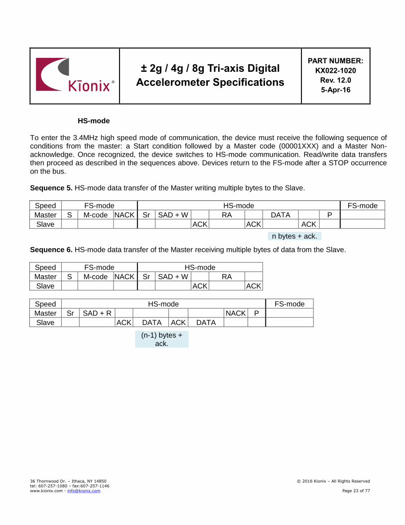
I2C Timing Diagram
Table 8: I2C Timing (Fast Mode)
Number Description MIN MAX Units
t0 SDA low to SCL low transition (Start event) 50
- ns
t1 SDA low to first SCL rising edge 100
- ns
t2 SCL pulse width: high 100
- ns t3 SCL pulse width: low 100
- ns
t4 SCL high before SDA falling edge (Start Repeated) 50
- ns
t5 SCL pulse width: high during a S/Sr/P event 100
- ns
t6 SCL high before SDA rising edge (Stop) 50
- ns
t7 SDA pulse width: high 25
- ns
t8 SDA valid to SCL rising edge 50
- ns
t9 SCL rising edge to SDA invalid 50
- ns
t10 SCL falling edge to SDA valid (when slave is transmitting) - 100
ns
t11 SCL falling edge to SDA invalid (when slave is transmitting) 0
- ns
Note Recommended I2C CLK 2.5
- us
± 2g / 4g / 8g Tri-axis Digital
Accelerometer Specifications
PART NUMBER:
KX022-1020
Rev. 12.0
5-Apr-16
36 Thornwood Dr. – Ithaca, NY 14850 © 2016 Kionix – All Rights Reserved tel: 607-257-1080 – fax:607-257-1146
www.kionix.com - [email protected] Page 25 of 77
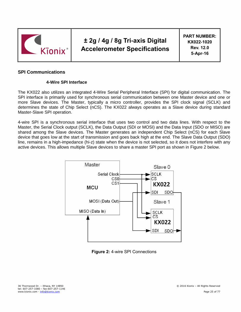
SPI Communications
4-Wire SPI Interface The KX022 also utilizes an integrated 4-Wire Serial Peripheral Interface (SPI) for digital communication. The SPI interface is primarily used for synchronous serial communication between one Master device and one or more Slave devices. The Master, typically a micro controller, provides the SPI clock signal (SCLK) and determines the state of Chip Select (nCS). The KX022 always operates as a Slave device during standard Master-Slave SPI operation. 4-wire SPI is a synchronous serial interface that uses two control and two data lines. With respect to the Master, the Serial Clock output (SCLK), the Data Output (SDI or MOSI) and the Data Input (SDO or MISO) are shared among the Slave devices. The Master generates an independent Chip Select (nCS) for each Slave device that goes low at the start of transmission and goes back high at the end. The Slave Data Output (SDO) line, remains in a high-impedance (hi-z) state when the device is not selected, so it does not interfere with any active devices. This allows multiple Slave devices to share a master SPI port as shown in Figure 2 below.
Figure 2: 4-wire SPI Connections
± 2g / 4g / 8g Tri-axis Digital
Accelerometer Specifications
PART NUMBER:
KX022-1020
Rev. 12.0
5-Apr-16
36 Thornwood Dr. – Ithaca, NY 14850 © 2016 Kionix – All Rights Reserved tel: 607-257-1080 – fax:607-257-1146
www.kionix.com - [email protected] Page 26 of 77
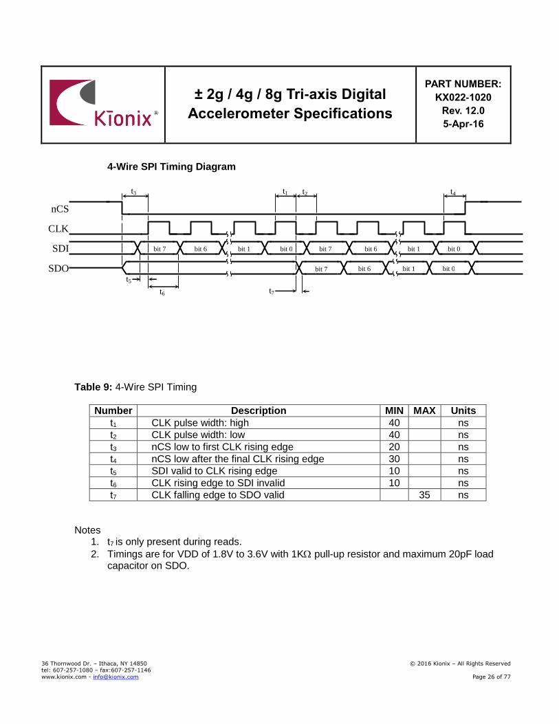
4-Wire SPI Timing Diagram
t
SDO
SDI
nCS
t3
CLK
bit 7 bit 6 bit 1
5
bit 0 bit 7
5
bit 6 bit 1
5
bit 0
bit 7
5
bit 6 bit 1
5
bit 0
t1 t2 t4
t5
t6 t7
Table 9: 4-Wire SPI Timing
Number Description MIN MAX Units
t1 CLK pulse width: high 40 ns
t2 CLK pulse width: low 40 ns
t3 nCS low to first CLK rising edge 20 ns
t4 nCS low after the final CLK rising edge 30 ns
t5 SDI valid to CLK rising edge 10 ns
t6 CLK rising edge to SDI invalid 10 ns
t7 CLK falling edge to SDO valid 35 ns
Notes 1. t7 is only present during reads.
2. Timings are for VDD of 1.8V to 3.6V with 1K pull-up resistor and maximum 20pF load capacitor on SDO.
± 2g / 4g / 8g Tri-axis Digital
Accelerometer Specifications
PART NUMBER:
KX022-1020
Rev. 12.0
5-Apr-16
36 Thornwood Dr. – Ithaca, NY 14850 © 2016 Kionix – All Rights Reserved tel: 607-257-1080 – fax:607-257-1146
www.kionix.com - [email protected] Page 27 of 77
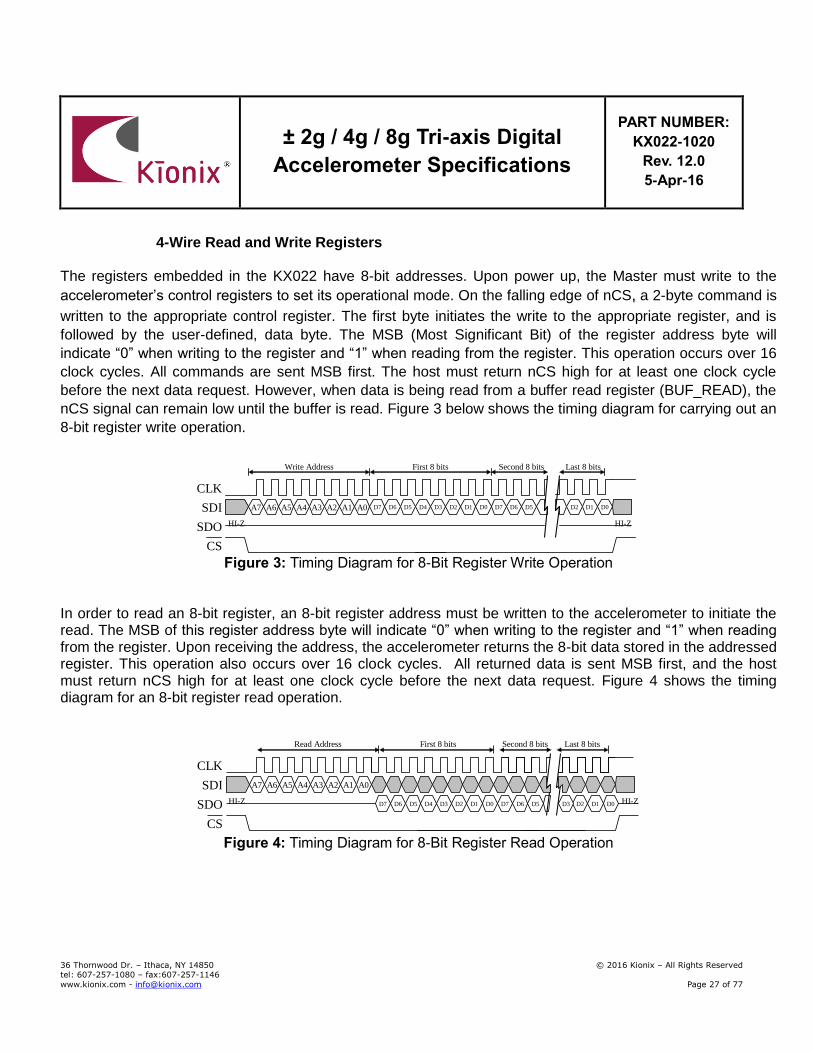
4-Wire Read and Write Registers The registers embedded in the KX022 have 8-bit addresses. Upon power up, the Master must write to the
accelerometer’s control registers to set its operational mode. On the falling edge of nCS, a 2-byte command is
written to the appropriate control register. The first byte initiates the write to the appropriate register, and is
followed by the user-defined, data byte. The MSB (Most Significant Bit) of the register address byte will
indicate “0” when writing to the register and “1” when reading from the register. This operation occurs over 16
clock cycles. All commands are sent MSB first. The host must return nCS high for at least one clock cycle
before the next data request. However, when data is being read from a buffer read register (BUF_READ), the
nCS signal can remain low until the buffer is read. Figure 3 below shows the timing diagram for carrying out an
8-bit register write operation.
A7 A6 A5 A4 A3 A2 A1 A0
SDO
SDI
CLK
CS
D2 D1
Write Address First 8 bits
HI-Z HI-Z
D7 D6 D5
Second 8 bits Last 8 bits
HI-Z
D0 D7 D6 D5 D4 D3 D2 D1 D0
Figure 3: Timing Diagram for 8-Bit Register Write Operation
In order to read an 8-bit register, an 8-bit register address must be written to the accelerometer to initiate the read. The MSB of this register address byte will indicate “0” when writing to the register and “1” when reading from the register. Upon receiving the address, the accelerometer returns the 8-bit data stored in the addressed register. This operation also occurs over 16 clock cycles. All returned data is sent MSB first, and the host must return nCS high for at least one clock cycle before the next data request. Figure 4 shows the timing diagram for an 8-bit register read operation.
SDO
SDI
CLK
CS
D2 D1 D5 D6 D7
A7 A6 A5 A4 A3 A2 A1 A0
Read Address
HI-Z
First 8 bits
HI-Z D2 D3 D4 D7 D0 D1 D6 D5
Last 8 bits
HI-Z D0 D3
Second 8 bits
Figure 4: Timing Diagram for 8-Bit Register Read Operation
± 2g / 4g / 8g Tri-axis Digital
Accelerometer Specifications
PART NUMBER:
KX022-1020
Rev. 12.0
5-Apr-16
36 Thornwood Dr. – Ithaca, NY 14850 © 2016 Kionix – All Rights Reserved tel: 607-257-1080 – fax:607-257-1146
www.kionix.com - [email protected] Page 28 of 77
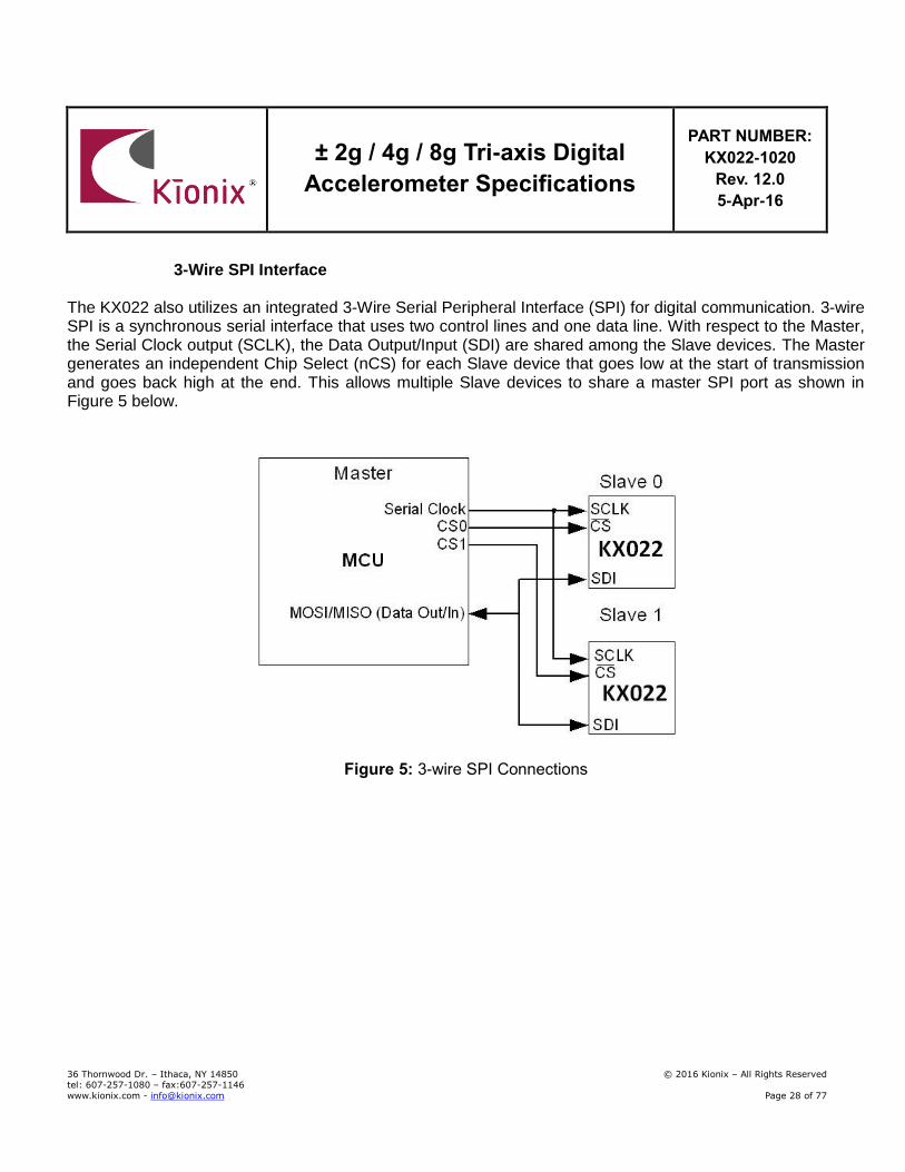
3-Wire SPI Interface The KX022 also utilizes an integrated 3-Wire Serial Peripheral Interface (SPI) for digital communication. 3-wire SPI is a synchronous serial interface that uses two control lines and one data line. With respect to the Master, the Serial Clock output (SCLK), the Data Output/Input (SDI) are shared among the Slave devices. The Master generates an independent Chip Select (nCS) for each Slave device that goes low at the start of transmission and goes back high at the end. This allows multiple Slave devices to share a master SPI port as shown in Figure 5 below.
Figure 5: 3-wire SPI Connections
± 2g / 4g / 8g Tri-axis Digital
Accelerometer Specifications
PART NUMBER:
KX022-1020
Rev. 12.0
5-Apr-16
36 Thornwood Dr. – Ithaca, NY 14850 © 2016 Kionix – All Rights Reserved tel: 607-257-1080 – fax:607-257-1146
www.kionix.com - [email protected] Page 29 of 77
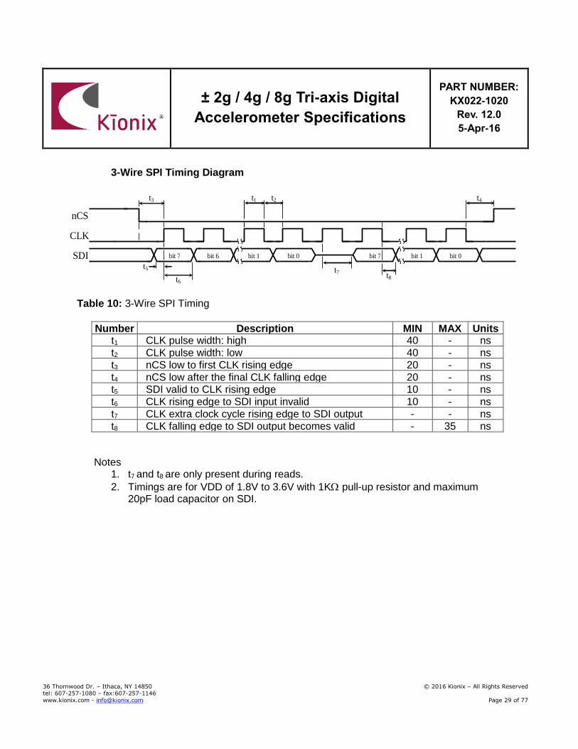
3-Wire SPI Timing Diagram
SDI
nCS
t3
CLK
bit 7 bit 6 bit 1
5
bit 0 bit 7 bit 1
5
bit 0
t1 t2
t7
t4
t5
t6 t8
Table 10: 3-Wire SPI Timing
Number Description MIN MAX Units t1 CLK pulse width: high 40 - ns
t2 CLK pulse width: low 40 - ns
t3 nCS low to first CLK rising edge 20 - ns
t4 nCS low after the final CLK falling edge 20 - ns t5 SDI valid to CLK rising edge 10 - ns
t6 CLK rising edge to SDI input invalid 10 - ns
t7 CLK extra clock cycle rising edge to SDI output becomes valid
- - ns
t8 CLK falling edge to SDI output becomes valid - 35 ns
Notes
1. t7 and t8 are only present during reads.
2. Timings are for VDD of 1.8V to 3.6V with 1K pull-up resistor and maximum 20pF load capacitor on SDI.
± 2g / 4g / 8g Tri-axis Digital
Accelerometer Specifications
PART NUMBER:
KX022-1020
Rev. 12.0
5-Apr-16
36 Thornwood Dr. – Ithaca, NY 14850 © 2016 Kionix – All Rights Reserved tel: 607-257-1080 – fax:607-257-1146
www.kionix.com - [email protected] Page 30 of 77
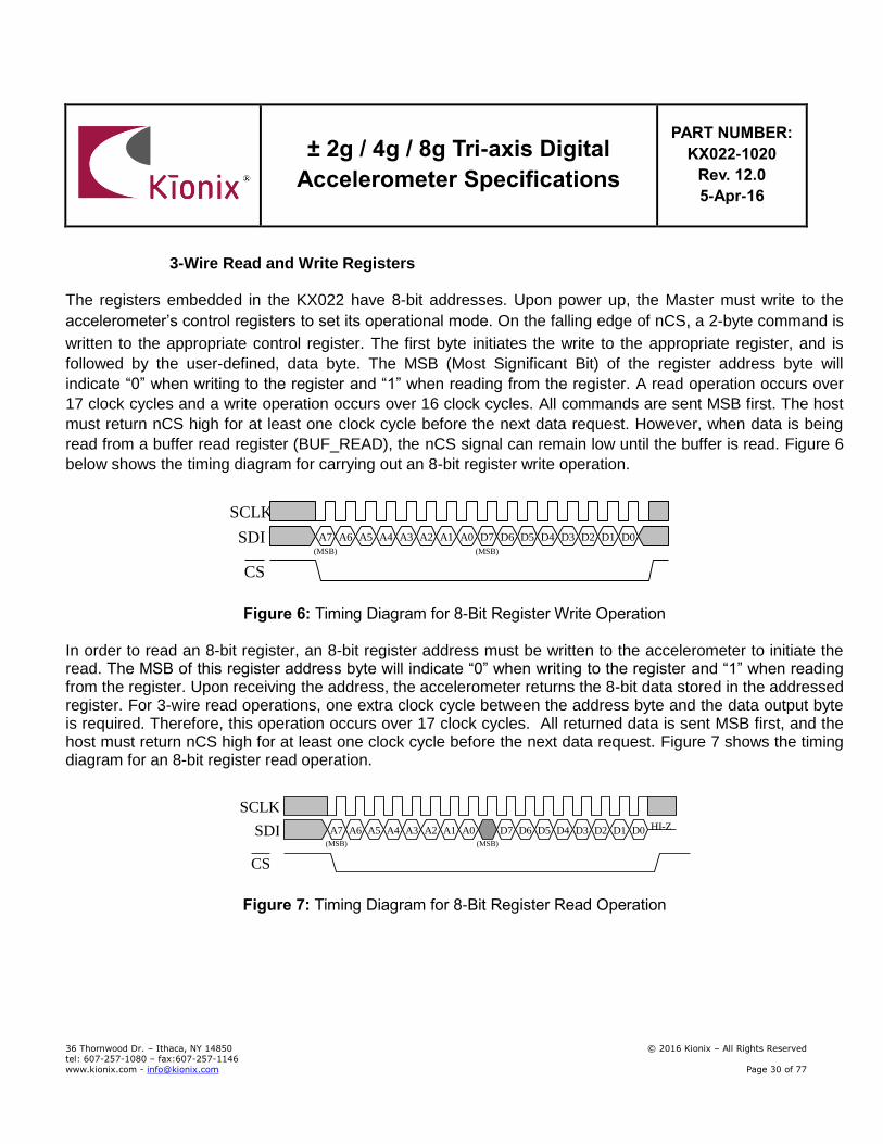
3-Wire Read and Write Registers The registers embedded in the KX022 have 8-bit addresses. Upon power up, the Master must write to the
accelerometer’s control registers to set its operational mode. On the falling edge of nCS, a 2-byte command is
written to the appropriate control register. The first byte initiates the write to the appropriate register, and is
followed by the user-defined, data byte. The MSB (Most Significant Bit) of the register address byte will
indicate “0” when writing to the register and “1” when reading from the register. A read operation occurs over
17 clock cycles and a write operation occurs over 16 clock cycles. All commands are sent MSB first. The host
must return nCS high for at least one clock cycle before the next data request. However, when data is being
read from a buffer read register (BUF_READ), the nCS signal can remain low until the buffer is read. Figure 6
below shows the timing diagram for carrying out an 8-bit register write operation.
A7 A6 A5 A4 A3 A2 A1 A0 SDI
SCLK
CS
D7 D6 D5 D4 D3 D2 D1 D0
(MSB) (MSB)
Figure 6: Timing Diagram for 8-Bit Register Write Operation
In order to read an 8-bit register, an 8-bit register address must be written to the accelerometer to initiate the read. The MSB of this register address byte will indicate “0” when writing to the register and “1” when reading from the register. Upon receiving the address, the accelerometer returns the 8-bit data stored in the addressed register. For 3-wire read operations, one extra clock cycle between the address byte and the data output byte is required. Therefore, this operation occurs over 17 clock cycles. All returned data is sent MSB first, and the host must return nCS high for at least one clock cycle before the next data request. Figure 7 shows the timing diagram for an 8-bit register read operation.
A7 A6 A5 A4 A3 A2 A1 A0 SDI
SCLK
CS
D7 D6 D5 D4 D3 D2 D1 D0 HI-Z
(MSB) (MSB)
Figure 7: Timing Diagram for 8-Bit Register Read Operation
± 2g / 4g / 8g Tri-axis Digital
Accelerometer Specifications
PART NUMBER:
KX022-1020
Rev. 12.0
5-Apr-16
36 Thornwood Dr. – Ithaca, NY 14850 © 2016 Kionix – All Rights Reserved tel: 607-257-1080 – fax:607-257-1146
www.kionix.com - [email protected] Page 31 of 77
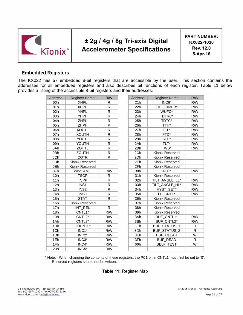
Embedded Registers
The KX022 has 57 embedded 8-bit registers that are accessible by the user. This section contains the addresses for all embedded registers and also describes bit functions of each register. Table 11 below provides a listing of the accessible 8-bit registers and their addresses.
Address Register Name R/W
Address Register Name R/W
00h XHPL R
21h INC6* R/W
01h XHPH R
22h TILT_TIMER* R/W
02h YHPL R
23h WUFC* R/W
03h YHPH R
24h TDTRC* R/W
04h ZHPL R
25h TDTC* R/W
05h ZHPH R
26h TTH* R/W
06h XOUTL R
27h TTL* R/W
07h XOUTH R
28h FTD* R/W
08h YOUTL R
29h STD* R/W
09h YOUTH R
2Ah TLT* R/W
0Ah ZOUTL R
2Bh TWS* R/W
0Bh ZOUTH R
2Ch Kionix Reserved
0Ch COTR R
2Dh Kionix Reserved
0Dh Kionix Reserved
2Eh Kionix Reserved
0Eh Kionix Reserved
2Fh Kionix Reserved
0Fh Who_AM_I R/W
30h ATH* R/W
10h TSCP R
31h Kionix Reserved
11h TSPP R
32h TILT_ANGLE_LL* R/W
12h INS1 R
33h TILT_ANGLE_HL* R/W
13h INS2 R
34h HYST_SET* R/W
14h INS3 R
35h LP_CNTL* R/W
15h STAT R
36h Kionix Reserved
16h Kionix Reserved
37h Kionix Reserved
17h INT_REL R
38h Kionix Reserved
18h CNTL1* R/W
39h Kionix Reserved
19h CNTL2* R/W
3Ah BUF_CNTL1* R/W
1Ah CNTL3* R/W
3Bh BUF_CNTL2* R/W
1Bh ODCNTL* R/W
3Ch BUF_STATUS_1 R
1Ch INC1* R/W
3Dh BUF_STATUS_2 R
1Dh INC2* R/W
3Eh BUF_CLEAR W
1Eh INC3* R/W
3Fh BUF_READ R
1Fh INC4* R/W
60h SELF_TEST W
20h INC5* R/W
* Note: - When changing the contents of these registers, the PC1 bit in CNTL1 must first be set to “0”. - Reserved registers should not be written.
Table 11: Register Map
± 2g / 4g / 8g Tri-axis Digital
Accelerometer Specifications
PART NUMBER:
KX022-1020
Rev. 12.0
5-Apr-16
36 Thornwood Dr. – Ithaca, NY 14850 © 2016 Kionix – All Rights Reserved tel: 607-257-1080 – fax:607-257-1146
www.kionix.com - [email protected] Page 32 of 77
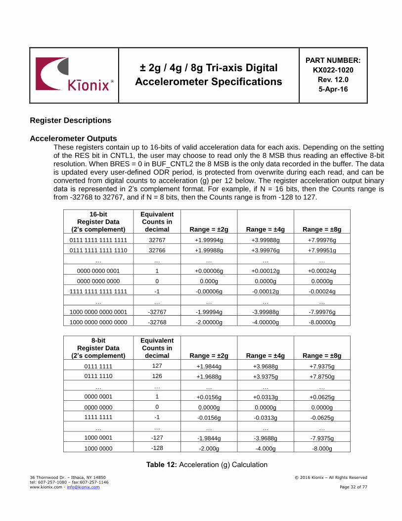
Register Descriptions Accelerometer Outputs
These registers contain up to 16-bits of valid acceleration data for each axis. Depending on the setting of the RES bit in CNTL1, the user may choose to read only the 8 MSB thus reading an effective 8-bit resolution. When BRES = 0 in BUF_CNTL2 the 8 MSB is the only data recorded in the buffer. The data is updated every user-defined ODR period, is protected from overwrite during each read, and can be converted from digital counts to acceleration (g) per 12 below. The register acceleration output binary data is represented in 2’s complement format. For example, if N = 16 bits, then the Counts range is from -32768 to 32767, and if N = 8 bits, then the Counts range is from -128 to 127.
16-bit Register Data
(2’s complement)
Equivalent Counts in decimal Range = ±2g Range = ±4g Range = ±8g
0111 1111 1111 1111 32767 +1.99994g +3.99988g +7.99976g
0111 1111 1111 1110 32766 +1.99988g +3.99976g +7.99951g
… … … … …
0000 0000 0001 1 +0.00006g +0.00012g +0.00024g
0000 0000 0000 0 0.000g 0.0000g 0.0000g
1111 1111 1111 1111 -1 -0.00006g -0.00012g -0.00024g
… … … … …
1000 0000 0000 0001 -32767 -1.99994g -3.99988g -7.99976g
1000 0000 0000 0000 -32768 -2.00000g -4.00000g -8.00000g
8-bit
Register Data (2’s complement)
Equivalent Counts in decimal Range = ±2g Range = ±4g Range = ±8g
0111 1111 127 +1.9844g +3.9688g +7.9375g
0111 1110 126 +1.9688g +3.9375g +7.8750g
… … … … …
0000 0001 1 +0.0156g +0.0313g +0.0625g
0000 0000 0 0.0000g 0.0000g 0.0000g
1111 1111 -1 -0.0156g -0.0313g -0.0625g
… … … … …
1000 0001 -127 -1.9844g -3.9688g -7.9375g
1000 0000 -128 -2.000g -4.000g -8.000g
Table 12: Acceleration (g) Calculation

± 2g / 4g / 8g Tri-axis Digital
Accelerometer Specifications
PART NUMBER:
KX022-1020
Rev. 12.0
5-Apr-16
36 Thornwood Dr. – Ithaca, NY 14850 © 2016 Kionix – All Rights Reserved tel: 607-257-1080 – fax:607-257-1146
www.kionix.com - [email protected] Page 33 of 77
XHP_L X-axis high pass filter accelerometer output least significant byte. Data is updated at the ODR frequency determined by OWUF in CNTL3.
R R R R R R R R
XHPD7 XHPD6 XHPD5 XHPD4 XHPD3 XHPD2 XHPD1 XHPD0
Bit7 Bit6 Bit5 Bit4 Bit3 Bit2 Bit1 Bit0
I2C Address: 0x00h
XHP_H X-axis high pass filter accelerometer output most significant byte. Data is updated at the ODR frequency determined by OWUF in CNTL3.
R R R R R R R R
XHPD15 XHPD14 XHPD13 XHPD12 XHPD11 XHPD10 XHPD9 XHPD8
Bit7 Bit6 Bit5 Bit4 Bit3 Bit2 Bit1 Bit0
I2C Address: 0x01h
YHP_L Y-axis high pass filter accelerometer output least significant byte. Data is updated at the ODR frequency determined by OWUF in CNTL3.
R R R R R R R R
YHPD7 YHPD6 YHPD5 YHPD4 YHPD3 YHPD2 YHPD1 YHPD0
Bit7 Bit6 Bit5 Bit4 Bit3 Bit2 Bit1 Bit0
I2C Address: 0x02h
YHP_H Y-axis high pass filter accelerometer output most significant byte. Data is updated at the ODR frequency determined by OWUF in CNTL3.
R R R R R R R R
YHPD15 YHPD14 YHPD13 YHPD12 YHPD11 YHPD10 YHPD9 YHPD8
Bit7 Bit6 Bit5 Bit4 Bit3 Bit2 Bit1 Bit0
I2C Address: 0x03h
± 2g / 4g / 8g Tri-axis Digital
Accelerometer Specifications
PART NUMBER:
KX022-1020
Rev. 12.0
5-Apr-16
36 Thornwood Dr. – Ithaca, NY 14850 © 2016 Kionix – All Rights Reserved tel: 607-257-1080 – fax:607-257-1146
www.kionix.com - [email protected] Page 34 of 77
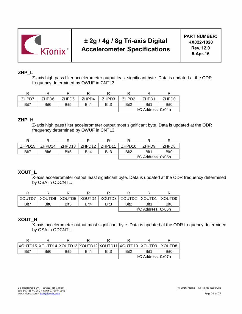
ZHP_L Z-axis high pass filter accelerometer output least significant byte. Data is updated at the ODR frequency determined by OWUF in CNTL3
R R R R R R R R
ZHPD7 ZHPD6 ZHPD5 ZHPD4 ZHPD3 ZHPD2 ZHPD1 ZHPD0
Bit7 Bit6 Bit5 Bit4 Bit3 Bit2 Bit1 Bit0
I2C Address: 0x04h
ZHP_H Z-axis high pass filter accelerometer output most significant byte. Data is updated at the ODR frequency determined by OWUF in CNTL3.
R R R R R R R R
ZHPD15 ZHPD14 ZHPD13 ZHPD12 ZHPD11 ZHPD10 ZHPD9 ZHPD8
Bit7 Bit6 Bit5 Bit4 Bit3 Bit2 Bit1 Bit0
I2C Address: 0x05h
XOUT_L X-axis accelerometer output least significant byte. Data is updated at the ODR frequency determined by OSA in ODCNTL.
R R R R R R R R
XOUTD7 XOUTD6 XOUTD5 XOUTD4 XOUTD3 XOUTD2 XOUTD1 XOUTD0
Bit7 Bit6 Bit5 Bit4 Bit3 Bit2 Bit1 Bit0
I2C Address: 0x06h
XOUT_H X-axis accelerometer output most significant byte. Data is updated at the ODR frequency determined by OSA in ODCNTL.
R R R R R R R R
XOUTD15 XOUTD14 XOUTD13 XOUTD12 XOUTD11 XOUTD10 XOUTD9 XOUTD8
Bit7 Bit6 Bit5 Bit4 Bit3 Bit2 Bit1 Bit0
I2C Address: 0x07h
± 2g / 4g / 8g Tri-axis Digital
Accelerometer Specifications
PART NUMBER:
KX022-1020
Rev. 12.0
5-Apr-16
36 Thornwood Dr. – Ithaca, NY 14850 © 2016 Kionix – All Rights Reserved tel: 607-257-1080 – fax:607-257-1146
www.kionix.com - [email protected] Page 35 of 77
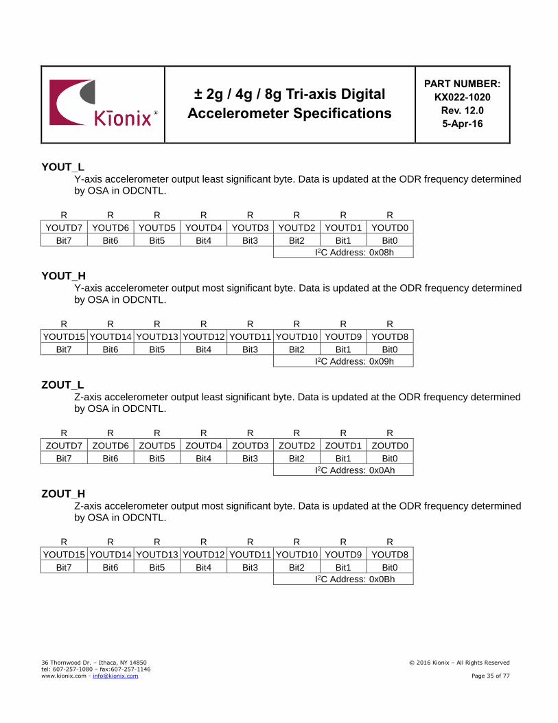
YOUT_L Y-axis accelerometer output least significant byte. Data is updated at the ODR frequency determined by OSA in ODCNTL.
R R R R R R R R
YOUTD7 YOUTD6 YOUTD5 YOUTD4 YOUTD3 YOUTD2 YOUTD1 YOUTD0
Bit7 Bit6 Bit5 Bit4 Bit3 Bit2 Bit1 Bit0
I2C Address: 0x08h
YOUT_H Y-axis accelerometer output most significant byte. Data is updated at the ODR frequency determined by OSA in ODCNTL.
R R R R R R R R
YOUTD15 YOUTD14 YOUTD13 YOUTD12 YOUTD11 YOUTD10 YOUTD9 YOUTD8
Bit7 Bit6 Bit5 Bit4 Bit3 Bit2 Bit1 Bit0
I2C Address: 0x09h
ZOUT_L Z-axis accelerometer output least significant byte. Data is updated at the ODR frequency determined by OSA in ODCNTL.
R R R R R R R R
ZOUTD7 ZOUTD6 ZOUTD5 ZOUTD4 ZOUTD3 ZOUTD2 ZOUTD1 ZOUTD0
Bit7 Bit6 Bit5 Bit4 Bit3 Bit2 Bit1 Bit0
I2C Address: 0x0Ah
ZOUT_H Z-axis accelerometer output most significant byte. Data is updated at the ODR frequency determined by OSA in ODCNTL.
R R R R R R R R
YOUTD15 YOUTD14 YOUTD13 YOUTD12 YOUTD11 YOUTD10 YOUTD9 YOUTD8
Bit7 Bit6 Bit5 Bit4 Bit3 Bit2 Bit1 Bit0
I2C Address: 0x0Bh
± 2g / 4g / 8g Tri-axis Digital
Accelerometer Specifications
PART NUMBER:
KX022-1020
Rev. 12.0
5-Apr-16
36 Thornwood Dr. – Ithaca, NY 14850 © 2016 Kionix – All Rights Reserved tel: 607-257-1080 – fax:607-257-1146
www.kionix.com - [email protected] Page 36 of 77
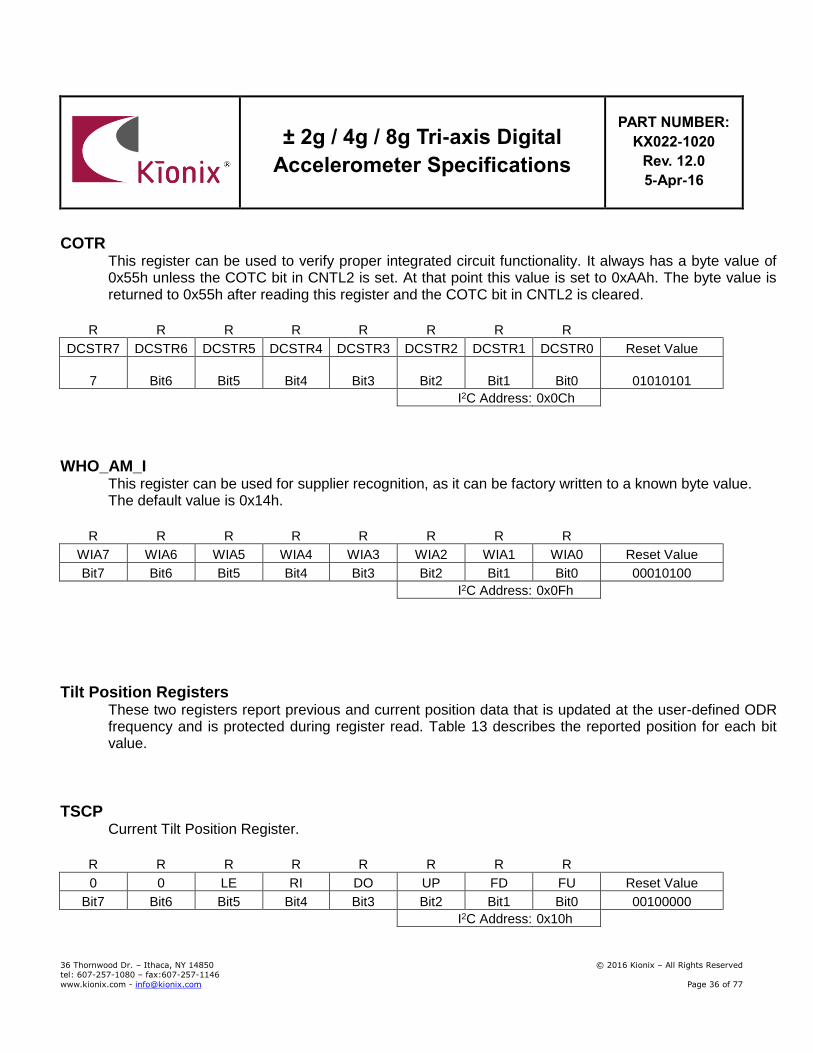
COTR This register can be used to verify proper integrated circuit functionality. It always has a byte value of 0x55h unless the COTC bit in CNTL2 is set. At that point this value is set to 0xAAh. The byte value is returned to 0x55h after reading this register and the COTC bit in CNTL2 is cleared.
R R R R R R R R
DCSTR7 DCSTR6 DCSTR5 DCSTR4 DCSTR3 DCSTR2 DCSTR1 DCSTR0 Reset Value
7 Bit6 Bit5 Bit4 Bit3 Bit2 Bit1 Bit0 01010101
I2C Address: 0x0Ch
WHO_AM_I This register can be used for supplier recognition, as it can be factory written to a known byte value. The default value is 0x14h.
R R R R R R R R
WIA7 WIA6 WIA5 WIA4 WIA3 WIA2 WIA1 WIA0 Reset Value
Bit7 Bit6 Bit5 Bit4 Bit3 Bit2 Bit1 Bit0 00010100
I2C Address: 0x0Fh
Tilt Position Registers These two registers report previous and current position data that is updated at the user-defined ODR frequency and is protected during register read. Table 13 describes the reported position for each bit value.
TSCP Current Tilt Position Register.
R R R R R R R R
0 0 LE RI DO UP FD FU Reset Value
Bit7 Bit6 Bit5 Bit4 Bit3 Bit2 Bit1 Bit0 00100000
I2C Address: 0x10h
± 2g / 4g / 8g Tri-axis Digital
Accelerometer Specifications
PART NUMBER:
KX022-1020
Rev. 12.0
5-Apr-16
36 Thornwood Dr. – Ithaca, NY 14850 © 2016 Kionix – All Rights Reserved tel: 607-257-1080 – fax:607-257-1146
www.kionix.com - [email protected] Page 37 of 77
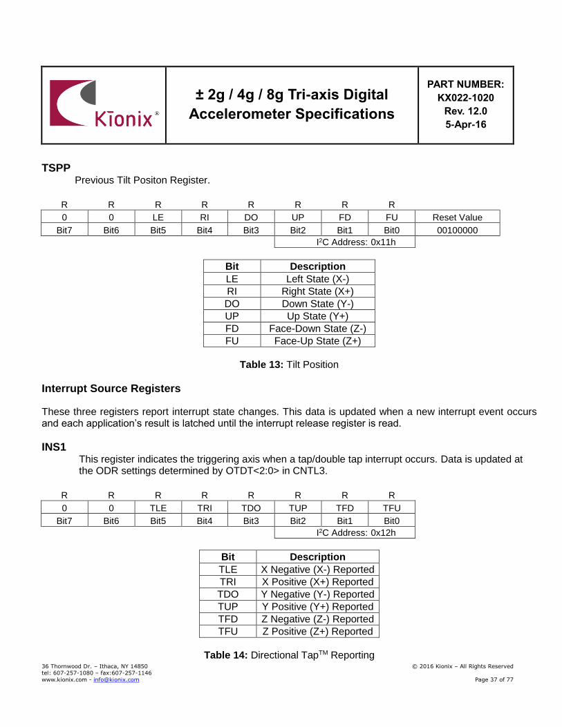
TSPP Previous Tilt Positon Register.
R R R R R R R R
0 0 LE RI DO UP FD FU Reset Value
Bit7 Bit6 Bit5 Bit4 Bit3 Bit2 Bit1 Bit0 00100000
I2C Address: 0x11h
Bit Description
LE Left State (X-)
RI Right State (X+)
DO Down State (Y-)
UP Up State (Y+)
FD Face-Down State (Z-)
FU Face-Up State (Z+)
Table 13: Tilt Position
Interrupt Source Registers
These three registers report interrupt state changes. This data is updated when a new interrupt event occurs and each application’s result is latched until the interrupt release register is read.
INS1 This register indicates the triggering axis when a tap/double tap interrupt occurs. Data is updated at
the ODR settings determined by OTDT<2:0> in CNTL3.
R R R R R R R R
0 0 TLE TRI TDO TUP TFD TFU
Bit7 Bit6 Bit5 Bit4 Bit3 Bit2 Bit1 Bit0
I2C Address: 0x12h
Bit Description
TLE X Negative (X-) Reported
TRI X Positive (X+) Reported
TDO Y Negative (Y-) Reported
TUP Y Positive (Y+) Reported
TFD Z Negative (Z-) Reported
TFU Z Positive (Z+) Reported
Table 14: Directional TapTM Reporting
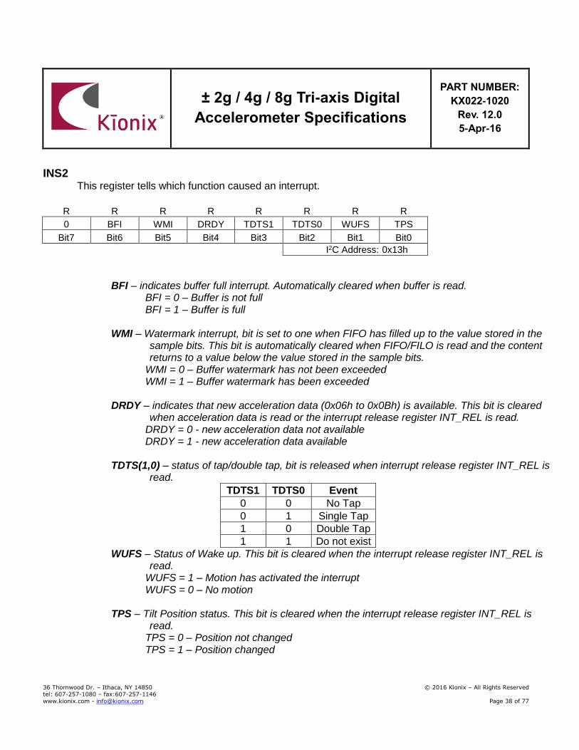
± 2g / 4g / 8g Tri-axis Digital
Accelerometer Specifications
PART NUMBER:
KX022-1020
Rev. 12.0
5-Apr-16
36 Thornwood Dr. – Ithaca, NY 14850 © 2016 Kionix – All Rights Reserved tel: 607-257-1080 – fax:607-257-1146
www.kionix.com - [email protected] Page 38 of 77
INS2 This register tells which function caused an interrupt.
R R R R R R R R
0 BFI WMI DRDY TDTS1 TDTS0 WUFS TPS
Bit7 Bit6 Bit5 Bit4 Bit3 Bit2 Bit1 Bit0
I2C Address: 0x13h
BFI – indicates buffer full interrupt. Automatically cleared when buffer is read. BFI = 0 – Buffer is not full BFI = 1 – Buffer is full
WMI – Watermark interrupt, bit is set to one when FIFO has filled up to the value stored in the
sample bits. This bit is automatically cleared when FIFO/FILO is read and the content returns to a value below the value stored in the sample bits.
WMI = 0 – Buffer watermark has not been exceeded WMI = 1 – Buffer watermark has been exceeded
DRDY – indicates that new acceleration data (0x06h to 0x0Bh) is available. This bit is cleared
when acceleration data is read or the interrupt release register INT_REL is read. DRDY = 0 - new acceleration data not available DRDY = 1 - new acceleration data available
TDTS(1,0) – status of tap/double tap, bit is released when interrupt release register INT_REL is
read.
TDTS1 TDTS0 Event
0 0 No Tap
0 1 Single Tap
1 0 Double Tap
1 1 Do not exist
WUFS – Status of Wake up. This bit is cleared when the interrupt release register INT_REL is read.
WUFS = 1 – Motion has activated the interrupt WUFS = 0 – No motion
TPS – Tilt Position status. This bit is cleared when the interrupt release register INT_REL is
read. TPS = 0 – Position not changed TPS = 1 – Position changed
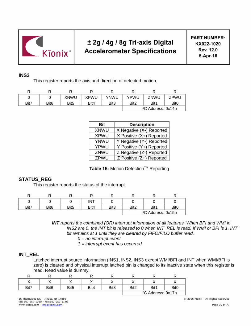
± 2g / 4g / 8g Tri-axis Digital
Accelerometer Specifications
PART NUMBER:
KX022-1020
Rev. 12.0
5-Apr-16
36 Thornwood Dr. – Ithaca, NY 14850 © 2016 Kionix – All Rights Reserved tel: 607-257-1080 – fax:607-257-1146
www.kionix.com - [email protected] Page 39 of 77
INS3 This register reports the axis and direction of detected motion.
R R R R R R R R
0 0 XNWU XPWU YNWU YPWU ZNWU ZPWU
Bit7 Bit6 Bit5 Bit4 Bit3 Bit2 Bit1 Bit0
I2C Address: 0x14h
Bit Description
XNWU X Negative (X-) Reported
XPWU X Positive (X+) Reported
YNWU Y Negative (Y-) Reported
YPWU Y Positive (Y+) Reported
ZNWU Z Negative (Z-) Reported
ZPWU Z Positive (Z+) Reported
Table 15: Motion DetectionTM Reporting
STATUS_REG This register reports the status of the interrupt.
R R R R R R R R
0 0 0 INT 0 0 0 0
Bit7 Bit6 Bit5 Bit4 Bit3 Bit2 Bit1 Bit0
I2C Address: 0x15h
INT reports the combined (OR) interrupt information of all features. When BFI and WMI in
INS2 are 0, the INT bit is released to 0 when INT_REL is read. If WMI or BFI is 1, INT bit remains at 1 until they are cleared by FIFO/FILO buffer read.
0 = no interrupt event 1 = interrupt event has occurred
INT_REL Latched interrupt source information (INS1, INS2, INS3 except WMI/BFI and INT when WMI/BFI is zero) is cleared and physical interrupt latched pin is changed to its inactive state when this register is read. Read value is dummy.
R R R R R R R R
X X X X X X X X
Bit7 Bit6 Bit5 Bit4 Bit3 Bit2 Bit1 Bit0
I2C Address: 0x17h
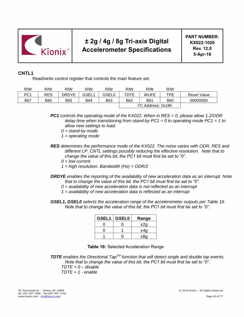
± 2g / 4g / 8g Tri-axis Digital
Accelerometer Specifications
PART NUMBER:
KX022-1020
Rev. 12.0
5-Apr-16
36 Thornwood Dr. – Ithaca, NY 14850 © 2016 Kionix – All Rights Reserved tel: 607-257-1080 – fax:607-257-1146
www.kionix.com - [email protected] Page 40 of 77
CNTL1 Read/write control register that controls the main feature set.
R/W R/W R/W R/W R/W R/W R/W R/W
PC1 RES DRDYE GSEL1 GSEL0 TDTE WUFE TPE Reset Value
Bit7 Bit6 Bit5 Bit4 Bit3 Bit2 Bit1 Bit0 00000000
I2C Address: 0x18h
PC1 controls the operating mode of the KX022. When in RES = 0, please allow 1.2/ODR
delay time when transitioning from stand-by PC1 = 0 to operating mode PC1 = 1 to allow new settings to load.
0 = stand-by mode 1 = operating mode
RES determines the performance mode of the KX022. The noise varies with ODR, RES and different LP_CNTL settings possibly reducing the effective resolution. Note that to change the value of this bit, the PC1 bit must first be set to “0”.
0 = low current. 1 = high resolution. Bandwidth (Hz) = ODR/2
DRDYE enables the reporting of the availability of new acceleration data as an interrupt. Note
that to change the value of this bit, the PC1 bit must first be set to “0”. 0 = availability of new acceleration data is not reflected as an interrupt 1 = availability of new acceleration data is reflected as an interrupt
GSEL1, GSEL0 selects the acceleration range of the accelerometer outputs per Table 16. Note that to change the value of this bit, the PC1 bit must first be set to “0”.
GSEL1 GSEL0 Range
0 0 ±2g
0 1 ±4g
1 0 ±8g
Table 16: Selected Acceleration Range
TDTE enables the Directional TapTM function that will detect single and double tap events.
Note that to change the value of this bit, the PC1 bit must first be set to “0”. TDTE = 0 – disable TDTE = 1 - enable
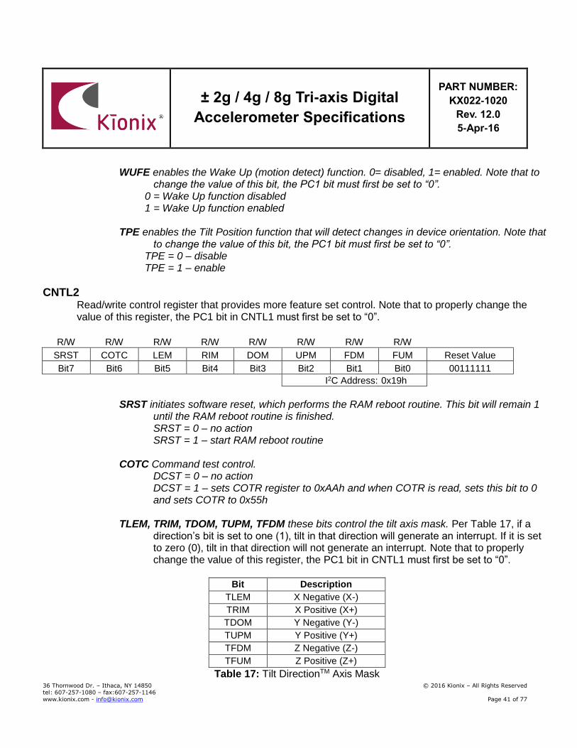
± 2g / 4g / 8g Tri-axis Digital
Accelerometer Specifications
PART NUMBER:
KX022-1020
Rev. 12.0
5-Apr-16
36 Thornwood Dr. – Ithaca, NY 14850 © 2016 Kionix – All Rights Reserved tel: 607-257-1080 – fax:607-257-1146
www.kionix.com - [email protected] Page 41 of 77
WUFE enables the Wake Up (motion detect) function. 0= disabled, 1= enabled. Note that to change the value of this bit, the PC1 bit must first be set to “0”.
0 = Wake Up function disabled 1 = Wake Up function enabled
TPE enables the Tilt Position function that will detect changes in device orientation. Note that
to change the value of this bit, the PC1 bit must first be set to “0”. TPE = 0 – disable TPE = 1 – enable
CNTL2 Read/write control register that provides more feature set control. Note that to properly change the value of this register, the PC1 bit in CNTL1 must first be set to “0”.
R/W R/W R/W R/W R/W R/W R/W R/W
SRST COTC LEM RIM DOM UPM FDM FUM Reset Value
Bit7 Bit6 Bit5 Bit4 Bit3 Bit2 Bit1 Bit0 00111111
I2C Address: 0x19h
SRST initiates software reset, which performs the RAM reboot routine. This bit will remain 1
until the RAM reboot routine is finished. SRST = 0 – no action SRST = 1 – start RAM reboot routine
COTC Command test control. DCST = 0 – no action DCST = 1 – sets COTR register to 0xAAh and when COTR is read, sets this bit to 0
and sets COTR to 0x55h TLEM, TRIM, TDOM, TUPM, TFDM these bits control the tilt axis mask. Per Table 17, if a
direction’s bit is set to one (1), tilt in that direction will generate an interrupt. If it is set to zero (0), tilt in that direction will not generate an interrupt. Note that to properly change the value of this register, the PC1 bit in CNTL1 must first be set to “0”.
Bit Description
TLEM X Negative (X-)
TRIM X Positive (X+)
TDOM Y Negative (Y-)
TUPM Y Positive (Y+)
TFDM Z Negative (Z-)
TFUM Z Positive (Z+)
Table 17: Tilt DirectionTM Axis Mask
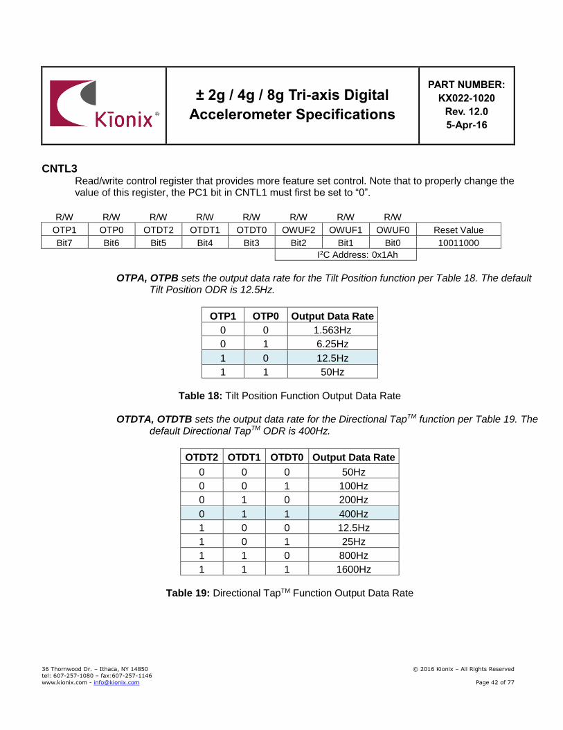
± 2g / 4g / 8g Tri-axis Digital
Accelerometer Specifications
PART NUMBER:
KX022-1020
Rev. 12.0
5-Apr-16
36 Thornwood Dr. – Ithaca, NY 14850 © 2016 Kionix – All Rights Reserved tel: 607-257-1080 – fax:607-257-1146
www.kionix.com - [email protected] Page 42 of 77
CNTL3 Read/write control register that provides more feature set control. Note that to properly change the value of this register, the PC1 bit in CNTL1 must first be set to “0”.
R/W R/W R/W R/W R/W R/W R/W R/W
OTP1 OTP0 OTDT2 OTDT1 OTDT0 OWUF2 OWUF1 OWUF0 Reset Value
Bit7 Bit6 Bit5 Bit4 Bit3 Bit2 Bit1 Bit0 10011000
I2C Address: 0x1Ah
OTPA, OTPB sets the output data rate for the Tilt Position function per Table 18. The default
Tilt Position ODR is 12.5Hz.
OTP1 OTP0 Output Data Rate
0 0 1.563Hz
0 1 6.25Hz
1 0 12.5Hz
1 1 50Hz
Table 18: Tilt Position Function Output Data Rate
OTDTA, OTDTB sets the output data rate for the Directional TapTM function per Table 19. The
default Directional TapTM ODR is 400Hz.
OTDT2 OTDT1 OTDT0 Output Data Rate
0 0 0 50Hz
0 0 1 100Hz
0 1 0 200Hz
0 1 1 400Hz
1 0 0 12.5Hz
1 0 1 25Hz
1 1 0 800Hz
1 1 1 1600Hz
Table 19: Directional TapTM Function Output Data Rate
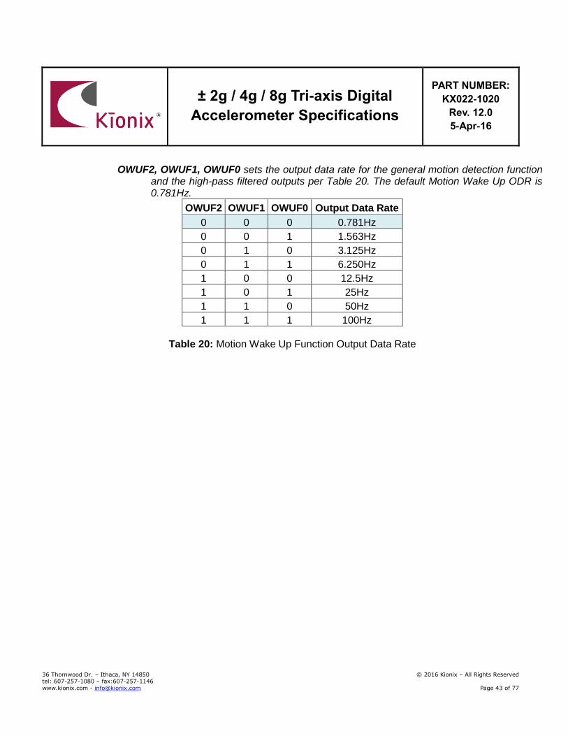
± 2g / 4g / 8g Tri-axis Digital
Accelerometer Specifications
PART NUMBER:
KX022-1020
Rev. 12.0
5-Apr-16
36 Thornwood Dr. – Ithaca, NY 14850 © 2016 Kionix – All Rights Reserved tel: 607-257-1080 – fax:607-257-1146
www.kionix.com - [email protected] Page 43 of 77
OWUF2, OWUF1, OWUF0 sets the output data rate for the general motion detection function and the high-pass filtered outputs per Table 20. The default Motion Wake Up ODR is 0.781Hz.
OWUF2 OWUF1 OWUF0 Output Data Rate
0 0 0 0.781Hz
0 0 1 1.563Hz
0 1 0 3.125Hz
0 1 1 6.250Hz
1 0 0 12.5Hz
1 0 1 25Hz
1 1 0 50Hz
1 1 1 100Hz
Table 20: Motion Wake Up Function Output Data Rate
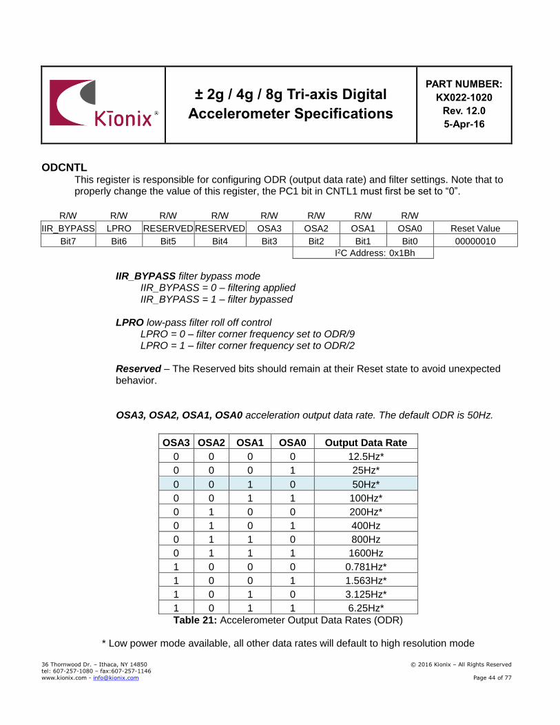
± 2g / 4g / 8g Tri-axis Digital
Accelerometer Specifications
PART NUMBER:
KX022-1020
Rev. 12.0
5-Apr-16
36 Thornwood Dr. – Ithaca, NY 14850 © 2016 Kionix – All Rights Reserved tel: 607-257-1080 – fax:607-257-1146
www.kionix.com - [email protected] Page 44 of 77
ODCNTL This register is responsible for configuring ODR (output data rate) and filter settings. Note that to properly change the value of this register, the PC1 bit in CNTL1 must first be set to “0”.
R/W R/W R/W R/W R/W R/W R/W R/W
IIR_BYPASS LPRO RESERVED RESERVED OSA3 OSA2 OSA1 OSA0 Reset Value
Bit7 Bit6 Bit5 Bit4 Bit3 Bit2 Bit1 Bit0 00000010
I2C Address: 0x1Bh
IIR_BYPASS filter bypass mode IIR_BYPASS = 0 – filtering applied IIR_BYPASS = 1 – filter bypassed LPRO low-pass filter roll off control LPRO = 0 – filter corner frequency set to ODR/9 LPRO = 1 – filter corner frequency set to ODR/2
Reserved – The Reserved bits should remain at their Reset state to avoid unexpected behavior.
OSA3, OSA2, OSA1, OSA0 acceleration output data rate. The default ODR is 50Hz.
OSA3 OSA2 OSA1 OSA0 Output Data Rate
0 0 0 0 12.5Hz*
0 0 0 1 25Hz*
0 0 1 0 50Hz*
0 0 1 1 100Hz*
0 1 0 0 200Hz*
0 1 0 1 400Hz
0 1 1 0 800Hz
0 1 1 1 1600Hz
1 0 0 0 0.781Hz*
1 0 0 1 1.563Hz*
1 0 1 0 3.125Hz*
1 0 1 1 6.25Hz*
Table 21: Accelerometer Output Data Rates (ODR)
* Low power mode available, all other data rates will default to high resolution mode
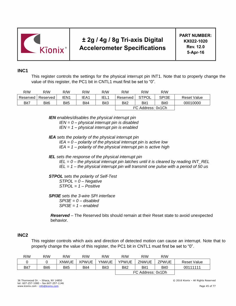
± 2g / 4g / 8g Tri-axis Digital
Accelerometer Specifications
PART NUMBER:
KX022-1020
Rev. 12.0
5-Apr-16
36 Thornwood Dr. – Ithaca, NY 14850 © 2016 Kionix – All Rights Reserved tel: 607-257-1080 – fax:607-257-1146
www.kionix.com - [email protected] Page 45 of 77
INC1
This register controls the settings for the physical interrupt pin INT1. Note that to properly change the
value of this register, the PC1 bit in CNTL1 must first be set to “0”.
R/W R/W R/W R/W R/W R/W R/W R/W
Reserved Reserved IEN1 IEA1 IEL1 Reserved STPOL SPI3E Reset Value
Bit7 Bit6 Bit5 Bit4 Bit3 Bit2 Bit1 Bit0 00010000
I2C Address: 0x1Ch
IEN enables/disables the physical interrupt pin IEN = 0 – physical interrupt pin is disabled IEN = 1 – physical interrupt pin is enabled IEA sets the polarity of the physical interrupt pin IEA = 0 – polarity of the physical interrupt pin is active low IEA = 1 – polarity of the physical interrupt pin is active high IEL sets the response of the physical interrupt pin IEL = 0 – the physical interrupt pin latches until it is cleared by reading INT_REL IEL = 1 – the physical interrupt pin will transmit one pulse with a period of 50 us STPOL sets the polarity of Self-Test STPOL = 0 – Negative STPOL = 1 – Positive SPI3E sets the 3-wire SPI interface SPI3E = 0 – disabled SPI3E = 1 – enabled
Reserved – The Reserved bits should remain at their Reset state to avoid unexpected behavior.
INC2
This register controls which axis and direction of detected motion can cause an interrupt. Note that to
properly change the value of this register, the PC1 bit in CNTL1 must first be set to “0”.
R/W R/W R/W R/W R/W R/W R/W R/W
0 0 XNWUE XPWUE YNWUE YPWUE ZNWUE ZPWUE Reset Value
Bit7 Bit6 Bit5 Bit4 Bit3 Bit2 Bit1 Bit0 00111111
I2C Address: 0x1Dh
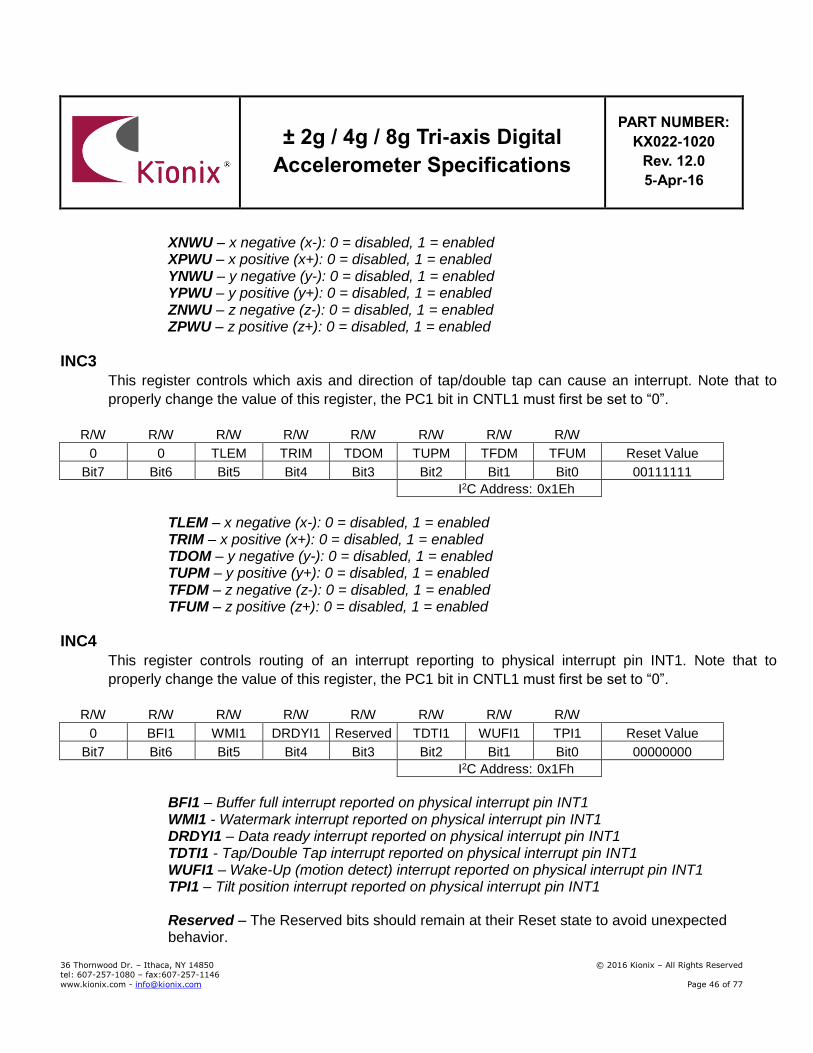
± 2g / 4g / 8g Tri-axis Digital
Accelerometer Specifications
PART NUMBER:
KX022-1020
Rev. 12.0
5-Apr-16
36 Thornwood Dr. – Ithaca, NY 14850 © 2016 Kionix – All Rights Reserved tel: 607-257-1080 – fax:607-257-1146
www.kionix.com - [email protected] Page 46 of 77
XNWU – x negative (x-): 0 = disabled, 1 = enabled XPWU – x positive (x+): 0 = disabled, 1 = enabled YNWU – y negative (y-): 0 = disabled, 1 = enabled YPWU – y positive (y+): 0 = disabled, 1 = enabled ZNWU – z negative (z-): 0 = disabled, 1 = enabled ZPWU – z positive (z+): 0 = disabled, 1 = enabled
INC3
This register controls which axis and direction of tap/double tap can cause an interrupt. Note that to
properly change the value of this register, the PC1 bit in CNTL1 must first be set to “0”.
R/W R/W R/W R/W R/W R/W R/W R/W
0 0 TLEM TRIM TDOM TUPM TFDM TFUM Reset Value
Bit7 Bit6 Bit5 Bit4 Bit3 Bit2 Bit1 Bit0 00111111
I2C Address: 0x1Eh
TLEM – x negative (x-): 0 = disabled, 1 = enabled TRIM – x positive (x+): 0 = disabled, 1 = enabled TDOM – y negative (y-): 0 = disabled, 1 = enabled TUPM – y positive (y+): 0 = disabled, 1 = enabled TFDM – z negative (z-): 0 = disabled, 1 = enabled TFUM – z positive (z+): 0 = disabled, 1 = enabled
INC4
This register controls routing of an interrupt reporting to physical interrupt pin INT1. Note that to
properly change the value of this register, the PC1 bit in CNTL1 must first be set to “0”.
R/W R/W R/W R/W R/W R/W R/W R/W
0 BFI1 WMI1 DRDYI1 Reserved TDTI1 WUFI1 TPI1 Reset Value
Bit7 Bit6 Bit5 Bit4 Bit3 Bit2 Bit1 Bit0 00000000
I2C Address: 0x1Fh
BFI1 – Buffer full interrupt reported on physical interrupt pin INT1 WMI1 - Watermark interrupt reported on physical interrupt pin INT1 DRDYI1 – Data ready interrupt reported on physical interrupt pin INT1 TDTI1 - Tap/Double Tap interrupt reported on physical interrupt pin INT1 WUFI1 – Wake-Up (motion detect) interrupt reported on physical interrupt pin INT1 TPI1 – Tilt position interrupt reported on physical interrupt pin INT1
Reserved – The Reserved bits should remain at their Reset state to avoid unexpected behavior.
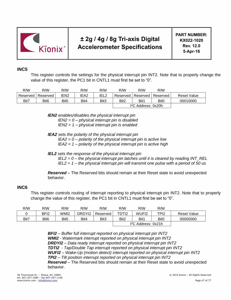
± 2g / 4g / 8g Tri-axis Digital
Accelerometer Specifications
PART NUMBER:
KX022-1020
Rev. 12.0
5-Apr-16
36 Thornwood Dr. – Ithaca, NY 14850 © 2016 Kionix – All Rights Reserved tel: 607-257-1080 – fax:607-257-1146
www.kionix.com - [email protected] Page 47 of 77
INC5
This register controls the settings for the physical interrupt pin INT2. Note that to properly change the
value of this register, the PC1 bit in CNTL1 must first be set to “0”.
R/W R/W R/W R/W R/W R/W R/W R/W
Reserved Reserved IEN2 IEA2 IEL2 Reserved Reserved Reserved Reset Value
Bit7 Bit6 Bit5 Bit4 Bit3 Bit2 Bit1 Bit0 00010000
I2C Address: 0x20h
IEN2 enables/disables the physical interrupt pin IEN2 = 0 – physical interrupt pin is disabled IEN2 = 1 – physical interrupt pin is enabled IEA2 sets the polarity of the physical interrupt pin IEA2 = 0 – polarity of the physical interrupt pin is active low IEA2 = 1 – polarity of the physical interrupt pin is active high IEL2 sets the response of the physical interrupt pin IEL2 = 0 – the physical interrupt pin latches until it is cleared by reading INT_REL IEL2 = 1 – the physical interrupt pin will transmit one pulse with a period of 50 us
Reserved – The Reserved bits should remain at their Reset state to avoid unexpected behavior.
INC6
This register controls routing of interrupt reporting to physical interrupt pin INT2. Note that to properly
change the value of this register, the PC1 bit in CNTL1 must first be set to “0”.
R/W R/W R/W R/W R/W R/W R/W R/W
0 BFI2 WMI2 DRDYI2 Reserved TDTI2 WUFI2 TPI2 Reset Value
Bit7 Bit6 Bit5 Bit4 Bit3 Bit2 Bit1 Bit0 00000000
I2C Address: 0x21h
BFI2 – Buffer full interrupt reported on physical interrupt pin INT2 WMI2 - Watermark interrupt reported on physical interrupt pin INT2 DRDYI2 – Data ready interrupt reported on physical interrupt pin INT2 TDTI2 - Tap/Double Tap interrupt reported on physical interrupt pin INT2 WUFI2 – Wake-Up (motion detect) interrupt reported on physical interrupt pin INT2 TPI2 – Tilt position interrupt reported on physical interrupt pin INT2 Reserved – The Reserved bits should remain at their Reset state to avoid unexpected behavior.
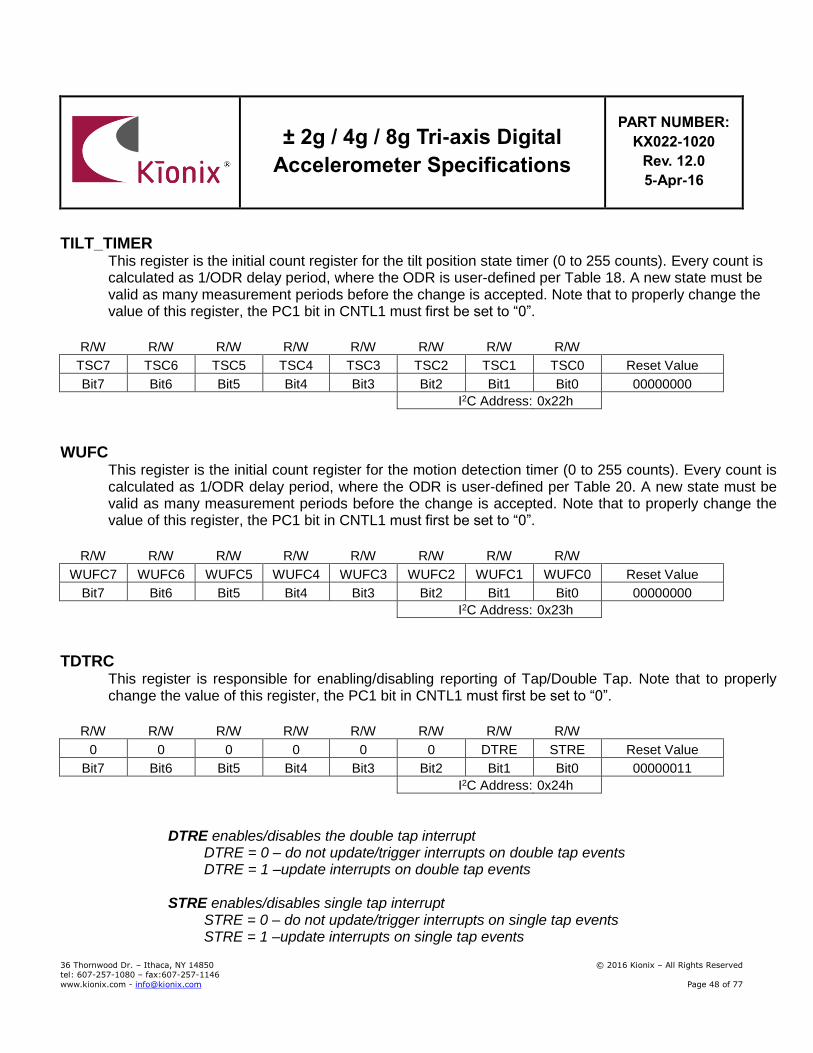
± 2g / 4g / 8g Tri-axis Digital
Accelerometer Specifications
PART NUMBER:
KX022-1020
Rev. 12.0
5-Apr-16
36 Thornwood Dr. – Ithaca, NY 14850 © 2016 Kionix – All Rights Reserved tel: 607-257-1080 – fax:607-257-1146
www.kionix.com - [email protected] Page 48 of 77
TILT_TIMER This register is the initial count register for the tilt position state timer (0 to 255 counts). Every count is calculated as 1/ODR delay period, where the ODR is user-defined per Table 18. A new state must be valid as many measurement periods before the change is accepted. Note that to properly change the value of this register, the PC1 bit in CNTL1 must first be set to “0”.
R/W R/W R/W R/W R/W R/W R/W R/W
TSC7 TSC6 TSC5 TSC4 TSC3 TSC2 TSC1 TSC0 Reset Value
Bit7 Bit6 Bit5 Bit4 Bit3 Bit2 Bit1 Bit0 00000000
I2C Address: 0x22h
WUFC This register is the initial count register for the motion detection timer (0 to 255 counts). Every count is calculated as 1/ODR delay period, where the ODR is user-defined per Table 20. A new state must be valid as many measurement periods before the change is accepted. Note that to properly change the value of this register, the PC1 bit in CNTL1 must first be set to “0”.
R/W R/W R/W R/W R/W R/W R/W R/W
WUFC7 WUFC6 WUFC5 WUFC4 WUFC3 WUFC2 WUFC1 WUFC0 Reset Value
Bit7 Bit6 Bit5 Bit4 Bit3 Bit2 Bit1 Bit0 00000000
I2C Address: 0x23h
TDTRC This register is responsible for enabling/disabling reporting of Tap/Double Tap. Note that to properly change the value of this register, the PC1 bit in CNTL1 must first be set to “0”.
R/W R/W R/W R/W R/W R/W R/W R/W
0 0 0 0 0 0 DTRE STRE Reset Value
Bit7 Bit6 Bit5 Bit4 Bit3 Bit2 Bit1 Bit0 00000011
I2C Address: 0x24h
DTRE enables/disables the double tap interrupt DTRE = 0 – do not update/trigger interrupts on double tap events DTRE = 1 –update interrupts on double tap events STRE enables/disables single tap interrupt STRE = 0 – do not update/trigger interrupts on single tap events STRE = 1 –update interrupts on single tap events
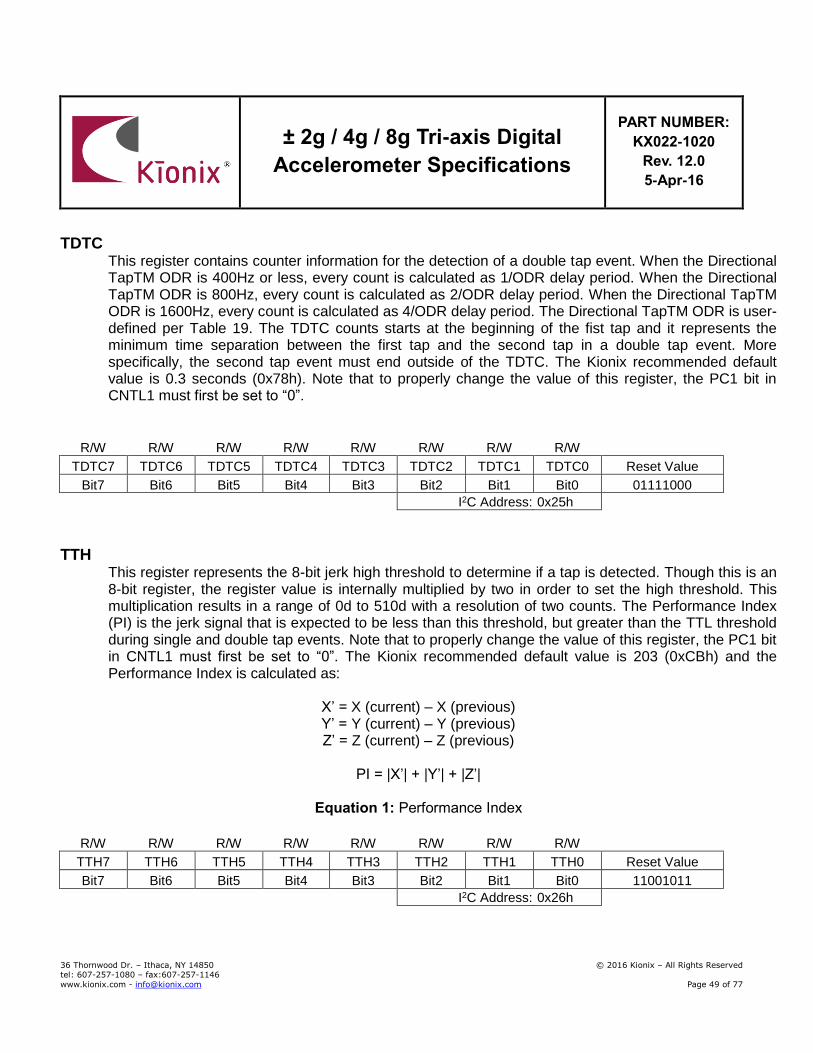
± 2g / 4g / 8g Tri-axis Digital
Accelerometer Specifications
PART NUMBER:
KX022-1020
Rev. 12.0
5-Apr-16
36 Thornwood Dr. – Ithaca, NY 14850 © 2016 Kionix – All Rights Reserved tel: 607-257-1080 – fax:607-257-1146
www.kionix.com - [email protected] Page 49 of 77
TDTC This register contains counter information for the detection of a double tap event. When the Directional TapTM ODR is 400Hz or less, every count is calculated as 1/ODR delay period. When the Directional TapTM ODR is 800Hz, every count is calculated as 2/ODR delay period. When the Directional TapTM ODR is 1600Hz, every count is calculated as 4/ODR delay period. The Directional TapTM ODR is user-defined per Table 19. The TDTC counts starts at the beginning of the fist tap and it represents the minimum time separation between the first tap and the second tap in a double tap event. More specifically, the second tap event must end outside of the TDTC. The Kionix recommended default value is 0.3 seconds (0x78h). Note that to properly change the value of this register, the PC1 bit in CNTL1 must first be set to “0”.
R/W R/W R/W R/W R/W R/W R/W R/W
TDTC7 TDTC6 TDTC5 TDTC4 TDTC3 TDTC2 TDTC1 TDTC0 Reset Value
Bit7 Bit6 Bit5 Bit4 Bit3 Bit2 Bit1 Bit0 01111000
I2C Address: 0x25h
TTH
This register represents the 8-bit jerk high threshold to determine if a tap is detected. Though this is an 8-bit register, the register value is internally multiplied by two in order to set the high threshold. This multiplication results in a range of 0d to 510d with a resolution of two counts. The Performance Index (PI) is the jerk signal that is expected to be less than this threshold, but greater than the TTL threshold during single and double tap events. Note that to properly change the value of this register, the PC1 bit in CNTL1 must first be set to “0”. The Kionix recommended default value is 203 (0xCBh) and the Performance Index is calculated as:
X’ = X (current) – X (previous) Y’ = Y (current) – Y (previous) Z’ = Z (current) – Z (previous)
PI = |X’| + |Y’| + |Z’|
Equation 1: Performance Index
R/W R/W R/W R/W R/W R/W R/W R/W
TTH7 TTH6 TTH5 TTH4 TTH3 TTH2 TTH1 TTH0 Reset Value
Bit7 Bit6 Bit5 Bit4 Bit3 Bit2 Bit1 Bit0 11001011
I2C Address: 0x26h
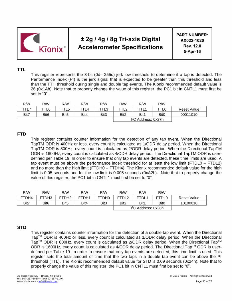
± 2g / 4g / 8g Tri-axis Digital
Accelerometer Specifications
PART NUMBER:
KX022-1020
Rev. 12.0
5-Apr-16
36 Thornwood Dr. – Ithaca, NY 14850 © 2016 Kionix – All Rights Reserved tel: 607-257-1080 – fax:607-257-1146
www.kionix.com - [email protected] Page 50 of 77
TTL This register represents the 8-bit (0d– 255d) jerk low threshold to determine if a tap is detected. The Performance Index (PI) is the jerk signal that is expected to be greater than this threshold and less than the TTH threshold during single and double tap events. The Kionix recommended default value is 26 (0x1Ah). Note that to properly change the value of this register, the PC1 bit in CNTL1 must first be set to “0”.
R/W R/W R/W R/W R/W R/W R/W R/W
TTL7 TTL6 TTL5 TTL4 TTL3 TTL2 TTL1 TTL0 Reset Value
Bit7 Bit6 Bit5 Bit4 Bit3 Bit2 Bit1 Bit0 00011010
I2C Address: 0x27h
FTD This register contains counter information for the detection of any tap event. When the Directional TapTM ODR is 400Hz or less, every count is calculated as 1/ODR delay period. When the Directional TapTM ODR is 800Hz, every count is calculated as 2/ODR delay period. When the Directional TapTM ODR is 1600Hz, every count is calculated as 4/ODR delay period. The Directional TapTM ODR is user-defined per Table 19. In order to ensure that only tap events are detected, these time limits are used. A tap event must be above the performance index threshold for at least the low limit (FTDL0 – FTDL2) and no more than the high limit (FTDH0 – FTDH4). The Kionix recommended default value for the high limit is 0.05 seconds and for the low limit is 0.005 seconds (0xA2h). Note that to properly change the value of this register, the PC1 bit in CNTL1 must first be set to “0”.
R/W R/W R/W R/W R/W R/W R/W R/W
FTDH4 FTDH3 FTDH2 FTDH1 FTDH0 FTDL2 FTDL1 FTDL0 Reset Value
Bit7 Bit6 Bit5 Bit4 Bit3 Bit2 Bit1 Bit0 10100010
I2C Address: 0x28h
STD This register contains counter information for the detection of a double tap event. When the Directional TapTM ODR is 400Hz or less, every count is calculated as 1/ODR delay period. When the Directional TapTM ODR is 800Hz, every count is calculated as 2/ODR delay period. When the Directional TapTM ODR is 1600Hz, every count is calculated as 4/ODR delay period. The Directional TapTM ODR is user-defined per Table 19. In order to ensure that only tap events are detected, this time limit is used. This register sets the total amount of time that the two taps in a double tap event can be above the PI threshold (TTL). The Kionix recommended default value for STD is 0.09 seconds (0x24h). Note that to properly change the value of this register, the PC1 bit in CNTL1 must first be set to “0”.
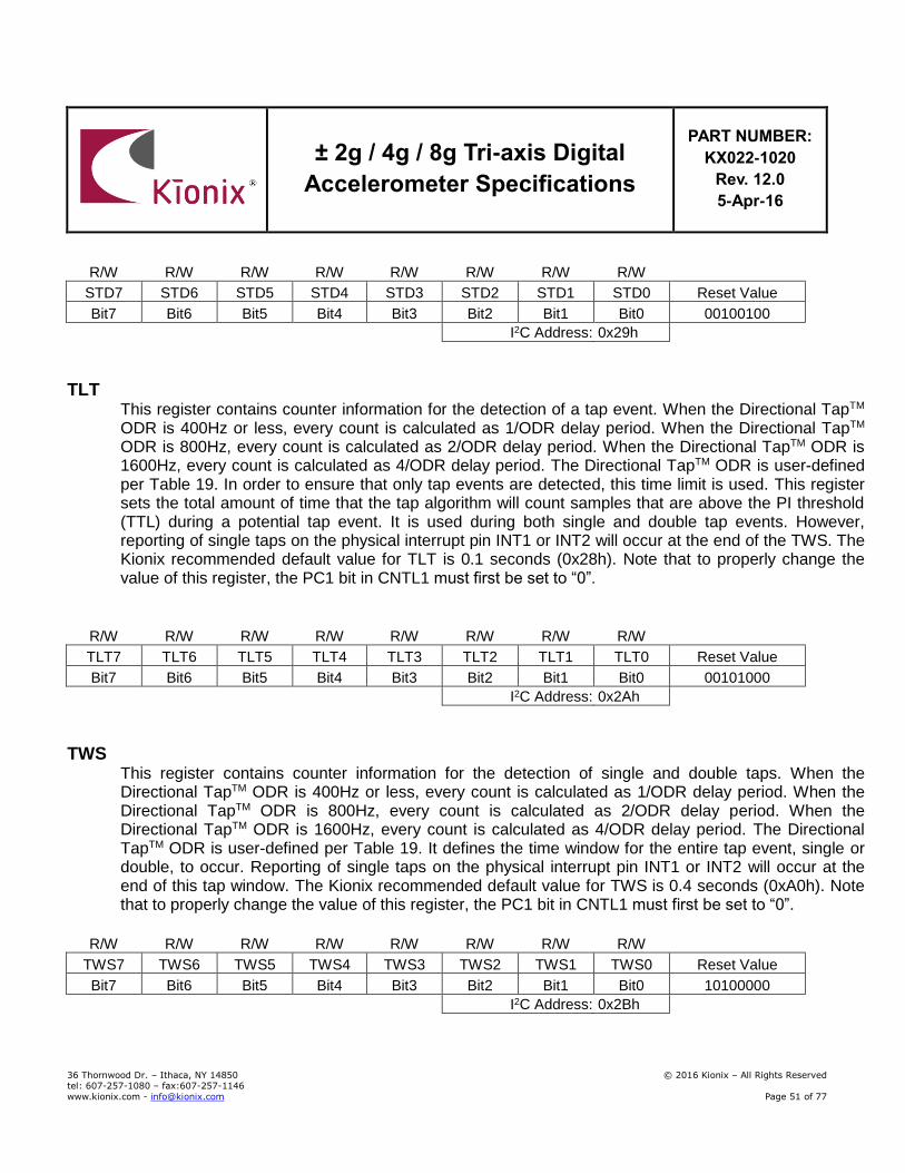
± 2g / 4g / 8g Tri-axis Digital
Accelerometer Specifications
PART NUMBER:
KX022-1020
Rev. 12.0
5-Apr-16
36 Thornwood Dr. – Ithaca, NY 14850 © 2016 Kionix – All Rights Reserved tel: 607-257-1080 – fax:607-257-1146
www.kionix.com - [email protected] Page 51 of 77
R/W R/W R/W R/W R/W R/W R/W R/W
STD7 STD6 STD5 STD4 STD3 STD2 STD1 STD0 Reset Value
Bit7 Bit6 Bit5 Bit4 Bit3 Bit2 Bit1 Bit0 00100100
I2C Address: 0x29h
TLT This register contains counter information for the detection of a tap event. When the Directional TapTM ODR is 400Hz or less, every count is calculated as 1/ODR delay period. When the Directional TapTM ODR is 800Hz, every count is calculated as 2/ODR delay period. When the Directional TapTM ODR is 1600Hz, every count is calculated as 4/ODR delay period. The Directional TapTM ODR is user-defined per Table 19. In order to ensure that only tap events are detected, this time limit is used. This register sets the total amount of time that the tap algorithm will count samples that are above the PI threshold (TTL) during a potential tap event. It is used during both single and double tap events. However, reporting of single taps on the physical interrupt pin INT1 or INT2 will occur at the end of the TWS. The Kionix recommended default value for TLT is 0.1 seconds (0x28h). Note that to properly change the value of this register, the PC1 bit in CNTL1 must first be set to “0”.
R/W R/W R/W R/W R/W R/W R/W R/W
TLT7 TLT6 TLT5 TLT4 TLT3 TLT2 TLT1 TLT0 Reset Value
Bit7 Bit6 Bit5 Bit4 Bit3 Bit2 Bit1 Bit0 00101000
I2C Address: 0x2Ah
TWS This register contains counter information for the detection of single and double taps. When the Directional TapTM ODR is 400Hz or less, every count is calculated as 1/ODR delay period. When the Directional TapTM ODR is 800Hz, every count is calculated as 2/ODR delay period. When the Directional TapTM ODR is 1600Hz, every count is calculated as 4/ODR delay period. The Directional TapTM ODR is user-defined per Table 19. It defines the time window for the entire tap event, single or double, to occur. Reporting of single taps on the physical interrupt pin INT1 or INT2 will occur at the end of this tap window. The Kionix recommended default value for TWS is 0.4 seconds (0xA0h). Note that to properly change the value of this register, the PC1 bit in CNTL1 must first be set to “0”.
R/W R/W R/W R/W R/W R/W R/W R/W
TWS7 TWS6 TWS5 TWS4 TWS3 TWS2 TWS1 TWS0 Reset Value
Bit7 Bit6 Bit5 Bit4 Bit3 Bit2 Bit1 Bit0 10100000
I2C Address: 0x2Bh
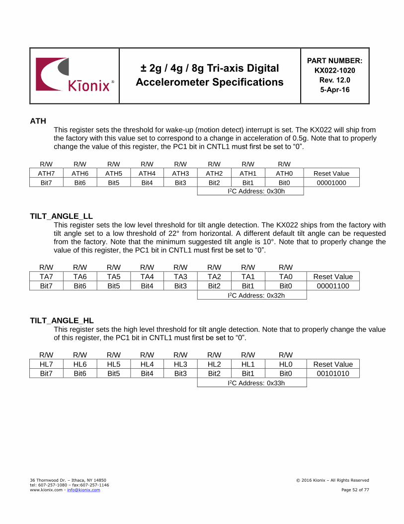
± 2g / 4g / 8g Tri-axis Digital
Accelerometer Specifications
PART NUMBER:
KX022-1020
Rev. 12.0
5-Apr-16
36 Thornwood Dr. – Ithaca, NY 14850 © 2016 Kionix – All Rights Reserved tel: 607-257-1080 – fax:607-257-1146
www.kionix.com - [email protected] Page 52 of 77
ATH This register sets the threshold for wake-up (motion detect) interrupt is set. The KX022 will ship from the factory with this value set to correspond to a change in acceleration of 0.5g. Note that to properly change the value of this register, the PC1 bit in CNTL1 must first be set to “0”.
R/W R/W R/W R/W R/W R/W R/W R/W
ATH7 ATH6 ATH5 ATH4 ATH3 ATH2 ATH1 ATH0 Reset Value
Bit7 Bit6 Bit5 Bit4 Bit3 Bit2 Bit1 Bit0 00001000
I2C Address: 0x30h
TILT_ANGLE_LL This register sets the low level threshold for tilt angle detection. The KX022 ships from the factory with tilt angle set to a low threshold of 22° from horizontal. A different default tilt angle can be requested from the factory. Note that the minimum suggested tilt angle is 10°. Note that to properly change the value of this register, the PC1 bit in CNTL1 must first be set to “0”.
R/W R/W R/W R/W R/W R/W R/W R/W
TA7 TA6 TA5 TA4 TA3 TA2 TA1 TA0 Reset Value
Bit7 Bit6 Bit5 Bit4 Bit3 Bit2 Bit1 Bit0 00001100
I2C Address: 0x32h
TILT_ANGLE_HL This register sets the high level threshold for tilt angle detection. Note that to properly change the value of this register, the PC1 bit in CNTL1 must first be set to “0”.
R/W R/W R/W R/W R/W R/W R/W R/W
HL7 HL6 HL5 HL4 HL3 HL2 HL1 HL0 Reset Value
Bit7 Bit6 Bit5 Bit4 Bit3 Bit2 Bit1 Bit0 00101010
I2C Address: 0x33h
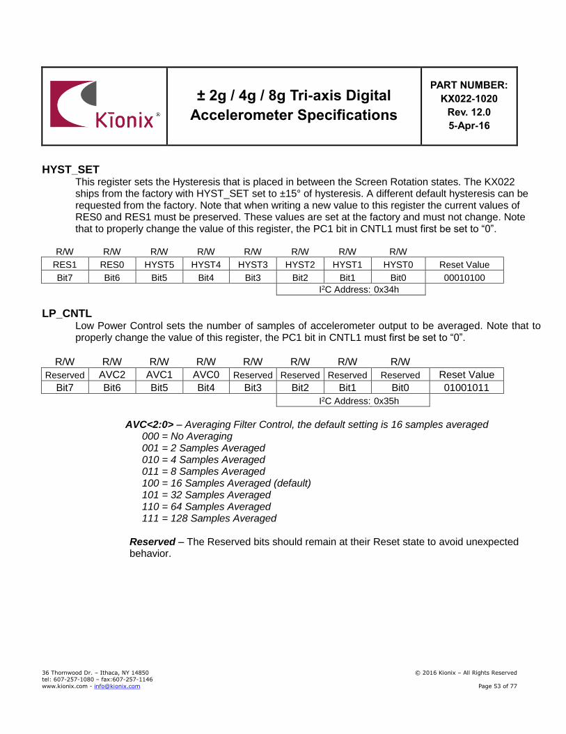
± 2g / 4g / 8g Tri-axis Digital
Accelerometer Specifications
PART NUMBER:
KX022-1020
Rev. 12.0
5-Apr-16
36 Thornwood Dr. – Ithaca, NY 14850 © 2016 Kionix – All Rights Reserved tel: 607-257-1080 – fax:607-257-1146
www.kionix.com - [email protected] Page 53 of 77
HYST_SET This register sets the Hysteresis that is placed in between the Screen Rotation states. The KX022 ships from the factory with HYST_SET set to ±15° of hysteresis. A different default hysteresis can be requested from the factory. Note that when writing a new value to this register the current values of RES0 and RES1 must be preserved. These values are set at the factory and must not change. Note that to properly change the value of this register, the PC1 bit in CNTL1 must first be set to “0”.
R/W R/W R/W R/W R/W R/W R/W R/W
RES1 RES0 HYST5 HYST4 HYST3 HYST2 HYST1 HYST0 Reset Value
Bit7 Bit6 Bit5 Bit4 Bit3 Bit2 Bit1 Bit0 00010100
I2C Address: 0x34h
LP_CNTL Low Power Control sets the number of samples of accelerometer output to be averaged. Note that to properly change the value of this register, the PC1 bit in CNTL1 must first be set to “0”.
R/W R/W R/W R/W R/W R/W R/W R/W
Reserved AVC2 AVC1 AVC0 Reserved Reserved Reserved Reserved Reset Value
Bit7 Bit6 Bit5 Bit4 Bit3 Bit2 Bit1 Bit0 01001011
I2C Address: 0x35h
AVC<2:0> – Averaging Filter Control, the default setting is 16 samples averaged
000 = No Averaging 001 = 2 Samples Averaged 010 = 4 Samples Averaged 011 = 8 Samples Averaged 100 = 16 Samples Averaged (default) 101 = 32 Samples Averaged 110 = 64 Samples Averaged 111 = 128 Samples Averaged
Reserved – The Reserved bits should remain at their Reset state to avoid unexpected behavior.
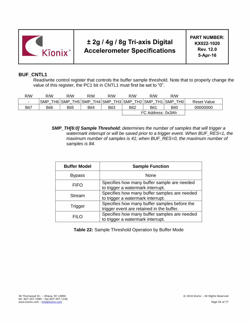
± 2g / 4g / 8g Tri-axis Digital
Accelerometer Specifications
PART NUMBER:
KX022-1020
Rev. 12.0
5-Apr-16
36 Thornwood Dr. – Ithaca, NY 14850 © 2016 Kionix – All Rights Reserved tel: 607-257-1080 – fax:607-257-1146
www.kionix.com - [email protected] Page 54 of 77
BUF_CNTL1 Read/write control register that controls the buffer sample threshold. Note that to properly change the value of this register, the PC1 bit in CNTL1 must first be set to “0”.
R/W R/W R/W R/W R/W R/W R/W R/W
- SMP_TH6 SMP_TH5 SMP_TH4 SMP_TH3 SMP_TH2 SMP_TH1 SMP_TH0 Reset Value
Bit7 Bit6 Bit5 Bit4 Bit3 Bit2 Bit1 Bit0 00000000
I2C Address: 0x3Ah
SMP_TH[6:0] Sample Threshold; determines the number of samples that will trigger a watermark interrupt or will be saved prior to a trigger event. When BUF_RES=1, the maximum number of samples is 41; when BUF_RES=0, the maximum number of samples is 84.
Buffer Model Sample Function
Bypass None
FIFO Specifies how many buffer sample are needed to trigger a watermark interrupt.
Stream Specifies how many buffer samples are needed to trigger a watermark interrupt.
Trigger Specifies how many buffer samples before the trigger event are retained in the buffer.
FILO Specifies how many buffer samples are needed to trigger a watermark interrupt.
Table 22: Sample Threshold Operation by Buffer Mode
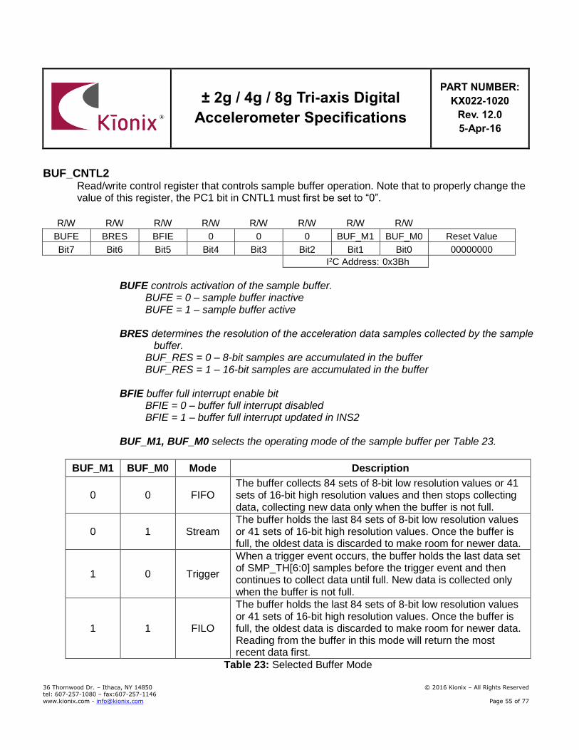
± 2g / 4g / 8g Tri-axis Digital
Accelerometer Specifications
PART NUMBER:
KX022-1020
Rev. 12.0
5-Apr-16
36 Thornwood Dr. – Ithaca, NY 14850 © 2016 Kionix – All Rights Reserved tel: 607-257-1080 – fax:607-257-1146
www.kionix.com - [email protected] Page 55 of 77
BUF_CNTL2 Read/write control register that controls sample buffer operation. Note that to properly change the value of this register, the PC1 bit in CNTL1 must first be set to “0”.
R/W R/W R/W R/W R/W R/W R/W R/W
BUFE BRES BFIE 0 0 0 BUF_M1 BUF_M0 Reset Value
Bit7 Bit6 Bit5 Bit4 Bit3 Bit2 Bit1 Bit0 00000000
I2C Address: 0x3Bh
BUFE controls activation of the sample buffer.
BUFE = 0 – sample buffer inactive BUFE = 1 – sample buffer active
BRES determines the resolution of the acceleration data samples collected by the sample buffer.
BUF_RES = 0 – 8-bit samples are accumulated in the buffer BUF_RES = 1 – 16-bit samples are accumulated in the buffer
BFIE buffer full interrupt enable bit BFIE = 0 – buffer full interrupt disabled BFIE = 1 – buffer full interrupt updated in INS2
BUF_M1, BUF_M0 selects the operating mode of the sample buffer per Table 23.
BUF_M1 BUF_M0 Mode Description
0 0 FIFO The buffer collects 84 sets of 8-bit low resolution values or 41 sets of 16-bit high resolution values and then stops collecting data, collecting new data only when the buffer is not full.
0 1 Stream The buffer holds the last 84 sets of 8-bit low resolution values or 41 sets of 16-bit high resolution values. Once the buffer is full, the oldest data is discarded to make room for newer data.
1 0 Trigger
When a trigger event occurs, the buffer holds the last data set of SMP_TH[6:0] samples before the trigger event and then continues to collect data until full. New data is collected only when the buffer is not full.
1 1 FILO
The buffer holds the last 84 sets of 8-bit low resolution values or 41 sets of 16-bit high resolution values. Once the buffer is full, the oldest data is discarded to make room for newer data. Reading from the buffer in this mode will return the most recent data first.
Table 23: Selected Buffer Mode
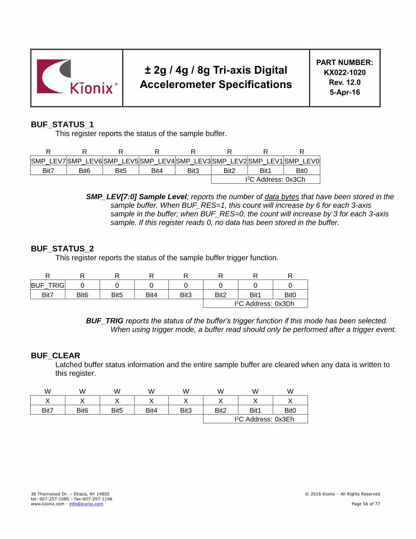
± 2g / 4g / 8g Tri-axis Digital
Accelerometer Specifications
PART NUMBER:
KX022-1020
Rev. 12.0
5-Apr-16
36 Thornwood Dr. – Ithaca, NY 14850 © 2016 Kionix – All Rights Reserved tel: 607-257-1080 – fax:607-257-1146
www.kionix.com - [email protected] Page 56 of 77
BUF_STATUS_1 This register reports the status of the sample buffer.
R R R R R R R R
SMP_LEV7 SMP_LEV6 SMP_LEV5 SMP_LEV4 SMP_LEV3 SMP_LEV2 SMP_LEV1 SMP_LEV0
Bit7 Bit6 Bit5 Bit4 Bit3 Bit2 Bit1 Bit0
I2C Address: 0x3Ch
SMP_LEV[7:0] Sample Level; reports the number of data bytes that have been stored in the
sample buffer. When BUF_RES=1, this count will increase by 6 for each 3-axis sample in the buffer; when BUF_RES=0, the count will increase by 3 for each 3-axis sample. If this register reads 0, no data has been stored in the buffer.
BUF_STATUS_2 This register reports the status of the sample buffer trigger function.
R R R R R R R R
BUF_TRIG 0 0 0 0 0 0 0
Bit7 Bit6 Bit5 Bit4 Bit3 Bit2 Bit1 Bit0
I2C Address: 0x3Dh
BUF_TRIG reports the status of the buffer’s trigger function if this mode has been selected.
When using trigger mode, a buffer read should only be performed after a trigger event.
BUF_CLEAR Latched buffer status information and the entire sample buffer are cleared when any data is written to this register.
W W W W W W W W
X X X X X X X X
Bit7 Bit6 Bit5 Bit4 Bit3 Bit2 Bit1 Bit0
I2C Address: 0x3Eh
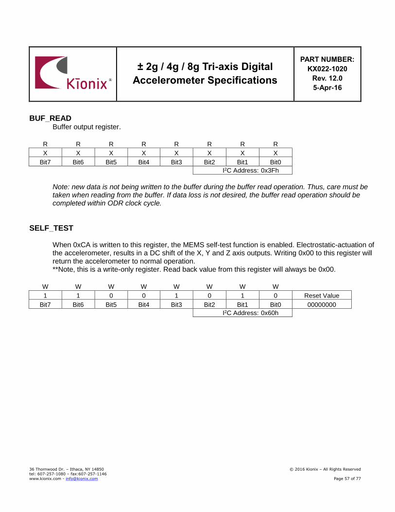
± 2g / 4g / 8g Tri-axis Digital
Accelerometer Specifications
PART NUMBER:
KX022-1020
Rev. 12.0
5-Apr-16
36 Thornwood Dr. – Ithaca, NY 14850 © 2016 Kionix – All Rights Reserved tel: 607-257-1080 – fax:607-257-1146
www.kionix.com - [email protected] Page 57 of 77
BUF_READ Buffer output register.
R R R R R R R R
X X X X X X X X
Bit7 Bit6 Bit5 Bit4 Bit3 Bit2 Bit1 Bit0
I2C Address: 0x3Fh
Note: new data is not being written to the buffer during the buffer read operation. Thus, care must be taken when reading from the buffer. If data loss is not desired, the buffer read operation should be completed within ODR clock cycle.
SELF_TEST
When 0xCA is written to this register, the MEMS self-test function is enabled. Electrostatic-actuation of the accelerometer, results in a DC shift of the X, Y and Z axis outputs. Writing 0x00 to this register will return the accelerometer to normal operation. **Note, this is a write-only register. Read back value from this register will always be 0x00.
W W W W W W W W
1 1 0 0 1 0 1 0 Reset Value
Bit7 Bit6 Bit5 Bit4 Bit3 Bit2 Bit1 Bit0 00000000
I2C Address: 0x60h
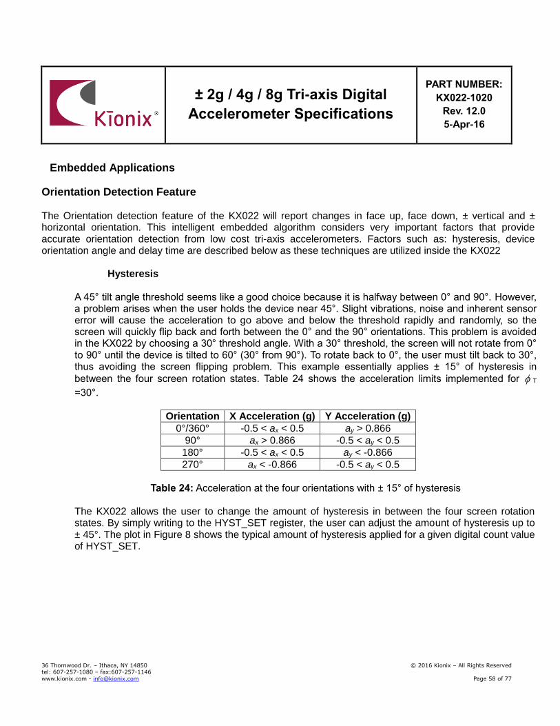
± 2g / 4g / 8g Tri-axis Digital
Accelerometer Specifications
PART NUMBER:
KX022-1020
Rev. 12.0
5-Apr-16
36 Thornwood Dr. – Ithaca, NY 14850 © 2016 Kionix – All Rights Reserved tel: 607-257-1080 – fax:607-257-1146
www.kionix.com - [email protected] Page 58 of 77
Embedded Applications
Orientation Detection Feature The Orientation detection feature of the KX022 will report changes in face up, face down, ± vertical and ± horizontal orientation. This intelligent embedded algorithm considers very important factors that provide accurate orientation detection from low cost tri-axis accelerometers. Factors such as: hysteresis, device orientation angle and delay time are described below as these techniques are utilized inside the KX022
Hysteresis A 45° tilt angle threshold seems like a good choice because it is halfway between 0° and 90°. However, a problem arises when the user holds the device near 45°. Slight vibrations, noise and inherent sensor error will cause the acceleration to go above and below the threshold rapidly and randomly, so the screen will quickly flip back and forth between the 0° and the 90° orientations. This problem is avoided in the KX022 by choosing a 30° threshold angle. With a 30° threshold, the screen will not rotate from 0° to 90° until the device is tilted to 60° (30° from 90°). To rotate back to 0°, the user must tilt back to 30°, thus avoiding the screen flipping problem. This example essentially applies ± 15° of hysteresis in
between the four screen rotation states. Table 24 shows the acceleration limits implemented for T
=30°.
Orientation X Acceleration (g) Y Acceleration (g)
0°/360° -0.5 < ax < 0.5 ay > 0.866
90° ax > 0.866 -0.5 < ay < 0.5
180° -0.5 < ax < 0.5 ay < -0.866
270° ax < -0.866 -0.5 < ay < 0.5
Table 24: Acceleration at the four orientations with ± 15° of hysteresis
The KX022 allows the user to change the amount of hysteresis in between the four screen rotation states. By simply writing to the HYST_SET register, the user can adjust the amount of hysteresis up to ± 45°. The plot in Figure 8 shows the typical amount of hysteresis applied for a given digital count value of HYST_SET.
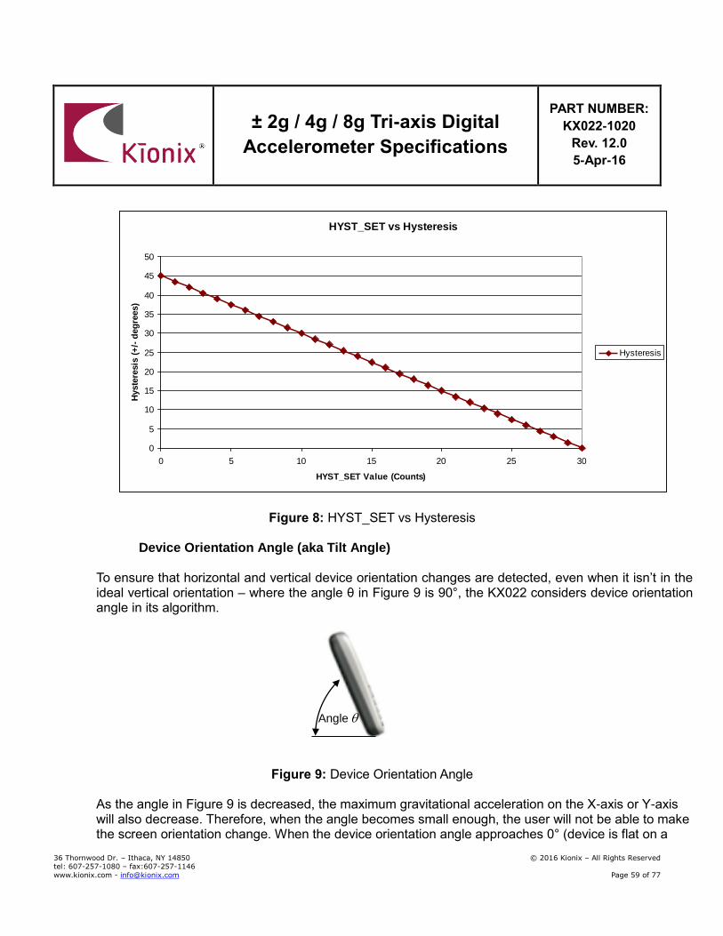
± 2g / 4g / 8g Tri-axis Digital
Accelerometer Specifications
PART NUMBER:
KX022-1020
Rev. 12.0
5-Apr-16
36 Thornwood Dr. – Ithaca, NY 14850 © 2016 Kionix – All Rights Reserved tel: 607-257-1080 – fax:607-257-1146
www.kionix.com - [email protected] Page 59 of 77
Figure 8: HYST_SET vs Hysteresis
Device Orientation Angle (aka Tilt Angle) To ensure that horizontal and vertical device orientation changes are detected, even when it isn’t in the ideal vertical orientation – where the angle θ in Figure 9 is 90°, the KX022 considers device orientation angle in its algorithm.
Figure 9: Device Orientation Angle
As the angle in Figure 9 is decreased, the maximum gravitational acceleration on the X-axis or Y-axis will also decrease. Therefore, when the angle becomes small enough, the user will not be able to make the screen orientation change. When the device orientation angle approaches 0° (device is flat on a
HYST_SET vs Hysteresis
0
5
10
15
20
25
30
35
40
45
50
0 5 10 15 20 25 30
HYST_SET Value (Counts)
Hyste
resis
(+
/- d
eg
rees)
Hysteresis
Angle
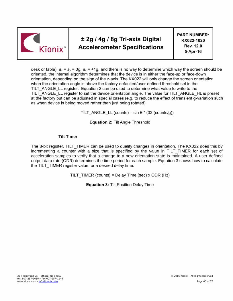
± 2g / 4g / 8g Tri-axis Digital
Accelerometer Specifications
PART NUMBER:
KX022-1020
Rev. 12.0
5-Apr-16
36 Thornwood Dr. – Ithaca, NY 14850 © 2016 Kionix – All Rights Reserved tel: 607-257-1080 – fax:607-257-1146
www.kionix.com - [email protected] Page 60 of 77
desk or table), ax = ay = 0g, az = +1g, and there is no way to determine which way the screen should be oriented, the internal algorithm determines that the device is in either the face-up or face-down orientation, depending on the sign of the z-axis. The KX022 will only change the screen orientation when the orientation angle is above the factory-defaulted/user-defined threshold set in the TILT_ANGLE_LL register. Equation 2 can be used to determine what value to write to the TILT_ANGLE_LL register to set the device orientation angle. The value for TILT_ANGLE_HL is preset at the factory but can be adjusted in special cases (e.g. to reduce the effect of transient g-variation such as when device is being moved rather than just being rotated).
TILT_ANGLE_LL (counts) = sin θ * (32 (counts/g))
Equation 2: Tilt Angle Threshold
Tilt Timer
The 8-bit register, TILT_TIMER can be used to qualify changes in orientation. The KX022 does this by incrementing a counter with a size that is specified by the value in TILT_TIMER for each set of acceleration samples to verify that a change to a new orientation state is maintained. A user defined output data rate (ODR) determines the time period for each sample. Equation 3 shows how to calculate the TILT_TIMER register value for a desired delay time.
TILT_TIMER (counts) = Delay Time (sec) x ODR (Hz)
Equation 3: Tilt Position Delay Time
± 2g / 4g / 8g Tri-axis Digital
Accelerometer Specifications
PART NUMBER:
KX022-1020
Rev. 12.0
5-Apr-16
36 Thornwood Dr. – Ithaca, NY 14850 © 2016 Kionix – All Rights Reserved tel: 607-257-1080 – fax:607-257-1146
www.kionix.com - [email protected] Page 61 of 77
Motion Interrupt Feature Description The Motion interrupt feature of the KX022 reports qualified changes in the high-pass filtered acceleration based on the Wake Up (ATH) threshold. If the high-pass filtered acceleration on any axis is greater than the user-defined wake up threshold (ATH), the device has transitioned from an inactive state to an active state. Equation 4 shows how to calculate the ATH register value for a desired wake up threshold. Note that this calculation varies based on the configured g-range of the part.
ATH (counts) = Wake Up Threshold (g) x 16 (counts/g)
Equation 4: Wake Up Threshold
An 8-bit raw unsigned value represents a counter that permits the user to qualify each active/inactive state change. Note that each WUFC Timer count qualifies 1 (one) user-defined ODR period (OWUF). Equation 5 shows how to calculate the WUFC register value for a desired wake up delay time.
WUFC (counts) = Wake Up Delay Time (sec) x OWUF (Hz)
Equation 5: Wake Up Delay Time
The latched motion interrupt response algorithm works as following: while the part is in inactive state, the algorithm evaluates differential measurement between each new acceleration data point with the preceding one and evaluates it against the ATH threshold. When the differential measurement is greater than ATH threshold, the wakeup counter starts the count. Differential measurements are now calculated based on the difference between the current acceleration and the acceleration when the counter started. The part will report that motion has occurred at the end of the count assuming each differential measurement has remained above the threshold. If at any moment during the count the differential measurement falls below the threshold, the counter will stop the count and the part will remain in inactive state. To illustrate how the algorithm works, consider the Figure 10 below that shows the latched response of the motion detection algorithm with WUF Timer (WUFC) set to 10 counts. Note how the difference between the acceleration sample marked in red and the one marked in green resulted in a differential measurements represented with orange bar being above the WUF threshold. At this point, the counter begins to count number of counts stored in WUFC register and the wakeup algorithm will evaluate the difference between each new acceleration measurement and the measurement marked in green that will remain a reference measurement for the duration of the counter count. At the end of the count, assuming all differential measurements were larger than WUF threshold, as is the case in the example showed in Figure 10, a motion event will be reported.
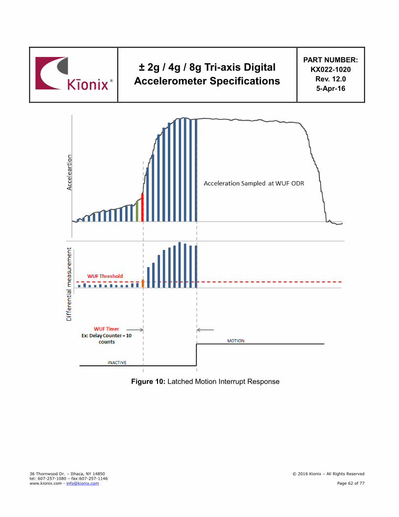
± 2g / 4g / 8g Tri-axis Digital
Accelerometer Specifications
PART NUMBER:
KX022-1020
Rev. 12.0
5-Apr-16
36 Thornwood Dr. – Ithaca, NY 14850 © 2016 Kionix – All Rights Reserved tel: 607-257-1080 – fax:607-257-1146
www.kionix.com - [email protected] Page 62 of 77
Figure 10: Latched Motion Interrupt Response
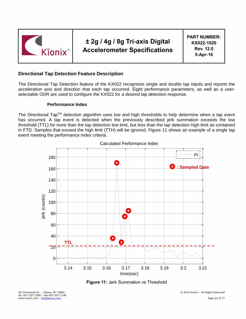
± 2g / 4g / 8g Tri-axis Digital
Accelerometer Specifications
PART NUMBER:
KX022-1020
Rev. 12.0
5-Apr-16
36 Thornwood Dr. – Ithaca, NY 14850 © 2016 Kionix – All Rights Reserved tel: 607-257-1080 – fax:607-257-1146
www.kionix.com - [email protected] Page 63 of 77
Directional Tap Detection Feature Description The Directional Tap Detection feature of the KX022 recognizes single and double tap inputs and reports the acceleration axis and direction that each tap occurred. Eight performance parameters, as well as a user-selectable ODR are used to configure the KX022 for a desired tap detection response.
Performance Index The Directional TapTM detection algorithm uses low and high thresholds to help determine when a tap event has occurred. A tap event is detected when the previously described jerk summation exceeds the low threshold (TTL) for more than the tap detection low limit, but less than the tap detection high limit as contained in FTD. Samples that exceed the high limit (TTH) will be ignored. Figure 11 shows an example of a single tap event meeting the performance index criteria.
Figure 11: Jerk Summation vs Threshold
3.14 3.15 3.16 3.17 3.18 3.19 3.2 3.21
0
20
40
60
80
100
120
140
160
180
Calculated Performance Index
time(sec)
jerk
(counts
)
PI
TTL
: Sampled Data
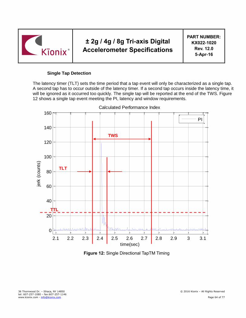
± 2g / 4g / 8g Tri-axis Digital
Accelerometer Specifications
PART NUMBER:
KX022-1020
Rev. 12.0
5-Apr-16
36 Thornwood Dr. – Ithaca, NY 14850 © 2016 Kionix – All Rights Reserved tel: 607-257-1080 – fax:607-257-1146
www.kionix.com - [email protected] Page 64 of 77
Single Tap Detection
The latency timer (TLT) sets the time period that a tap event will only be characterized as a single tap. A second tap has to occur outside of the latency timer. If a second tap occurs inside the latency time, it will be ignored as it occurred too quickly. The single tap will be reported at the end of the TWS. Figure 12 shows a single tap event meeting the PI, latency and window requirements.
Figure 12: Single Directional TapTM Timing
2.1 2.2 2.3 2.4 2.5 2.6 2.7 2.8 2.9 3 3.1
0
20
40
60
80
100
120
140
160
Calculated Performance Index
time(sec)
jerk
(counts
)
PI
TWS
TLT
TTL
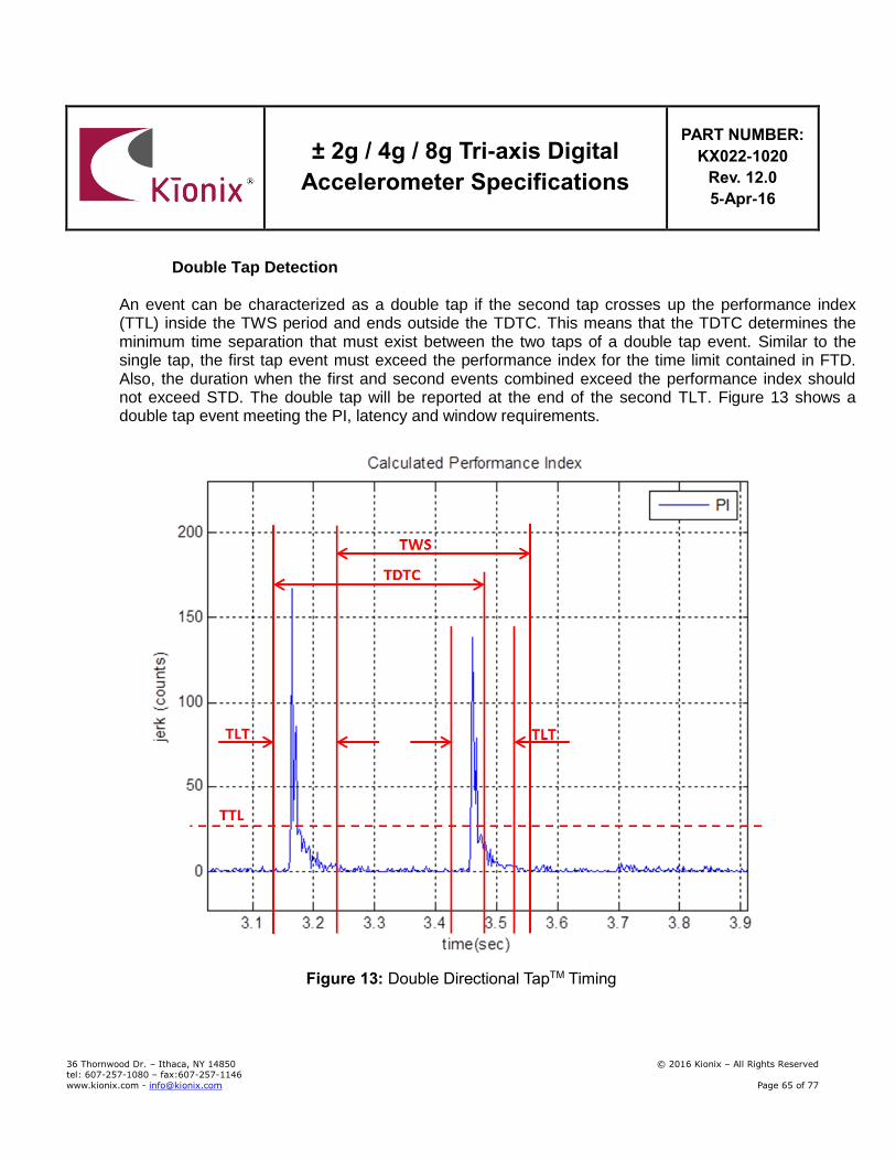
± 2g / 4g / 8g Tri-axis Digital
Accelerometer Specifications
PART NUMBER:
KX022-1020
Rev. 12.0
5-Apr-16
36 Thornwood Dr. – Ithaca, NY 14850 © 2016 Kionix – All Rights Reserved tel: 607-257-1080 – fax:607-257-1146
www.kionix.com - [email protected] Page 65 of 77
Double Tap Detection
An event can be characterized as a double tap if the second tap crosses up the performance index (TTL) inside the TWS period and ends outside the TDTC. This means that the TDTC determines the minimum time separation that must exist between the two taps of a double tap event. Similar to the single tap, the first tap event must exceed the performance index for the time limit contained in FTD. Also, the duration when the first and second events combined exceed the performance index should not exceed STD. The double tap will be reported at the end of the second TLT. Figure 13 shows a double tap event meeting the PI, latency and window requirements.
Figure 13: Double Directional TapTM Timing
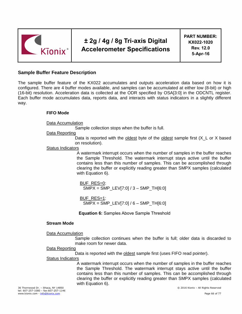
± 2g / 4g / 8g Tri-axis Digital
Accelerometer Specifications
PART NUMBER:
KX022-1020
Rev. 12.0
5-Apr-16
36 Thornwood Dr. – Ithaca, NY 14850 © 2016 Kionix – All Rights Reserved tel: 607-257-1080 – fax:607-257-1146
www.kionix.com - [email protected] Page 66 of 77
Sample Buffer Feature Description The sample buffer feature of the KX022 accumulates and outputs acceleration data based on how it is configured. There are 4 buffer modes available, and samples can be accumulated at either low (8-bit) or high (16-bit) resolution. Acceleration data is collected at the ODR specified by OSA[3:0] in the ODCNTL register. Each buffer mode accumulates data, reports data, and interacts with status indicators in a slightly different way.
FIFO Mode
Data Accumulation Sample collection stops when the buffer is full. Data Reporting
Data is reported with the oldest byte of the oldest sample first (X_L or X based on resolution).
Status Indicators A watermark interrupt occurs when the number of samples in the buffer reaches the Sample Threshold. The watermark interrupt stays active until the buffer contains less than this number of samples. This can be accomplished through clearing the buffer or explicitly reading greater than SMPX samples (calculated with Equation 6).
BUF_RES=0:
SMPX = SMP_LEV[7:0] / 3 – SMP_TH[6:0] BUF_RES=1:
SMPX = SMP_LEV[7:0] / 6 – SMP_TH[6:0]
Equation 6: Samples Above Sample Threshold
Stream Mode Data Accumulation Sample collection continues when the buffer is full; older data is discarded to make room for newer data. Data Reporting Data is reported with the oldest sample first (uses FIFO read pointer). Status Indicators
A watermark interrupt occurs when the number of samples in the buffer reaches the Sample Threshold. The watermark interrupt stays active until the buffer contains less than this number of samples. This can be accomplished through clearing the buffer or explicitly reading greater than SMPX samples (calculated with Equation 6).
± 2g / 4g / 8g Tri-axis Digital
Accelerometer Specifications
PART NUMBER:
KX022-1020
Rev. 12.0
5-Apr-16
36 Thornwood Dr. – Ithaca, NY 14850 © 2016 Kionix – All Rights Reserved tel: 607-257-1080 – fax:607-257-1146
www.kionix.com - [email protected] Page 67 of 77
Trigger Mode Data Accumulation
When a physical interrupt is caused by one of the digital engines, or when a logic high signal occurs on the TRIG pin, the trigger event is asserted and SMP_TH[6:0] samples prior to the event are retained. Sample collection continues until the buffer is full.
Data Reporting Data is reported with the oldest sample first (uses FIFO read pointer). Status Indicators
When a physical interrupt occurs and there are at least SMP_TH[6:0] samples in the buffer, BUF_TRIG in BUF_STATUS_2 is asserted.
FILO Mode
Data Accumulation Sample collection continues when the buffer is full; older data is discarded to make room for newer data. Data Reporting
Data is reported with the newest byte of the newest sample first (Z_H or Z based on resolution).
Status Indicators A watermark interrupt occurs when the number of samples in the buffer reaches the Sample Threshold. The watermark interrupt stays active until the buffer contains less than this number of samples. This can be accomplished through clearing the buffer or explicitly reading greater than SMPX samples (calculated with Equation 6).
Buffer Operation
The following diagrams illustrate the operation of the buffer conceptually. Actual physical implementation has been abstracted to offer a simplified explanation of how the different buffer modes operate. Figure 14 represents a high-resolution 3-axis sample within the buffer. Figure 15 - Figure 23 represent a 10-sample version of the buffer (for simplicity), with Sample Threshold set to 8.
Regardless of the selected mode, the buffer fills sequentially, one byte at a time. It it important to keep in mind that new data is not being written to the buffer during the buffer read operation. Thus, care must be taken when reading from the buffer. If data loss is not desired, the buffer read operation should be completed within ODR clock cycle.
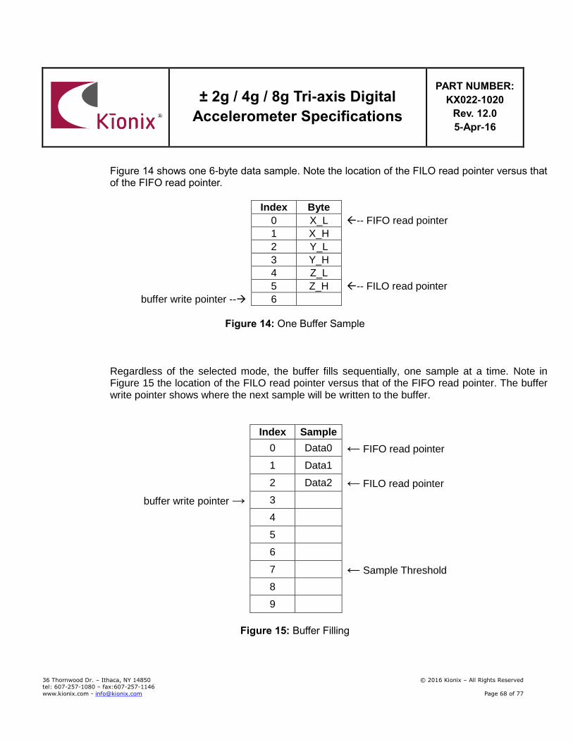
± 2g / 4g / 8g Tri-axis Digital
Accelerometer Specifications
PART NUMBER:
KX022-1020
Rev. 12.0
5-Apr-16
36 Thornwood Dr. – Ithaca, NY 14850 © 2016 Kionix – All Rights Reserved tel: 607-257-1080 – fax:607-257-1146
www.kionix.com - [email protected] Page 68 of 77
Figure 14 shows one 6-byte data sample. Note the location of the FILO read pointer versus that of the FIFO read pointer.
Index Byte
0 X_L -- FIFO read pointer
1 X_H
2 Y_L
3 Y_H
4 Z_L
5 Z_H -- FILO read pointer
buffer write pointer -- 6
Figure 14: One Buffer Sample
Regardless of the selected mode, the buffer fills sequentially, one sample at a time. Note in Figure 15 the location of the FILO read pointer versus that of the FIFO read pointer. The buffer write pointer shows where the next sample will be written to the buffer.
Index Sample
0 Data0 ← FIFO read pointer
1 Data1
2 Data2 ← FILO read pointer
buffer write pointer → 3
4
5
6
7 ← Sample Threshold
8
9
Figure 15: Buffer Filling
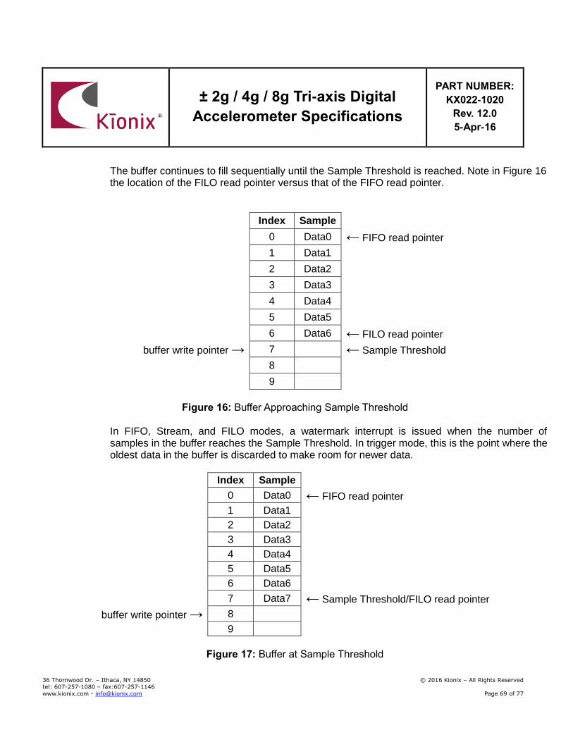
± 2g / 4g / 8g Tri-axis Digital
Accelerometer Specifications
PART NUMBER:
KX022-1020
Rev. 12.0
5-Apr-16
36 Thornwood Dr. – Ithaca, NY 14850 © 2016 Kionix – All Rights Reserved tel: 607-257-1080 – fax:607-257-1146
www.kionix.com - [email protected] Page 69 of 77
The buffer continues to fill sequentially until the Sample Threshold is reached. Note in Figure 16 the location of the FILO read pointer versus that of the FIFO read pointer.
Index Sample
0 Data0 ← FIFO read pointer 1 Data1
2 Data2
3 Data3
4 Data4
5 Data5
6 Data6 ← FILO read pointer
buffer write pointer → 7 ← Sample Threshold
8
9
Figure 16: Buffer Approaching Sample Threshold
In FIFO, Stream, and FILO modes, a watermark interrupt is issued when the number of samples in the buffer reaches the Sample Threshold. In trigger mode, this is the point where the oldest data in the buffer is discarded to make room for newer data.
Index Sample
0 Data0 ← FIFO read pointer 1 Data1
2 Data2
3 Data3
4 Data4
5 Data5
6 Data6
7 Data7 ← Sample Threshold/FILO read pointer
buffer write pointer → 8
9
Figure 17: Buffer at Sample Threshold
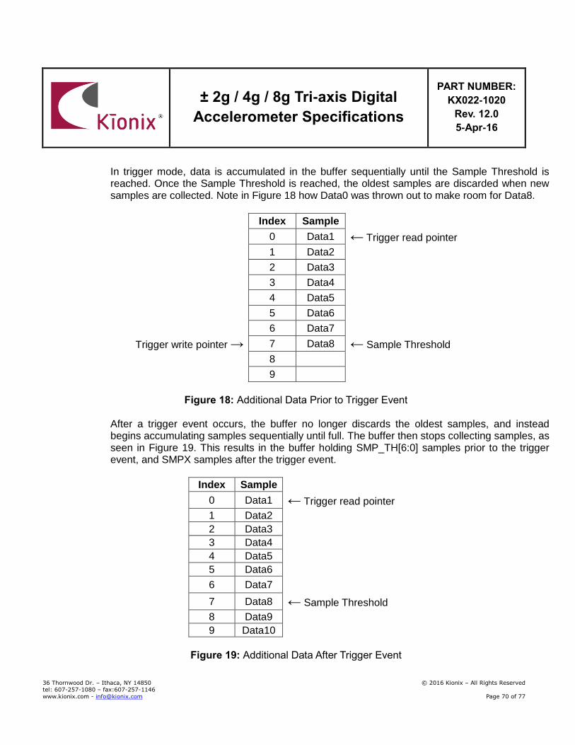
± 2g / 4g / 8g Tri-axis Digital
Accelerometer Specifications
PART NUMBER:
KX022-1020
Rev. 12.0
5-Apr-16
36 Thornwood Dr. – Ithaca, NY 14850 © 2016 Kionix – All Rights Reserved tel: 607-257-1080 – fax:607-257-1146
www.kionix.com - [email protected] Page 70 of 77
In trigger mode, data is accumulated in the buffer sequentially until the Sample Threshold is reached. Once the Sample Threshold is reached, the oldest samples are discarded when new samples are collected. Note in Figure 18 how Data0 was thrown out to make room for Data8.
Index Sample
0 Data1 ← Trigger read pointer 1 Data2
2 Data3
3 Data4
4 Data5
5 Data6
6 Data7
Trigger write pointer → 7 Data8 ← Sample Threshold
8
9
Figure 18: Additional Data Prior to Trigger Event
After a trigger event occurs, the buffer no longer discards the oldest samples, and instead begins accumulating samples sequentially until full. The buffer then stops collecting samples, as seen in Figure 19. This results in the buffer holding SMP_TH[6:0] samples prior to the trigger event, and SMPX samples after the trigger event.
Index Sample
0 Data1 ← Trigger read pointer 1 Data2
2 Data3
3 Data4
4 Data5
5 Data6
6 Data7
7 Data8 ← Sample Threshold 8 Data9
9 Data10
Figure 19: Additional Data After Trigger Event
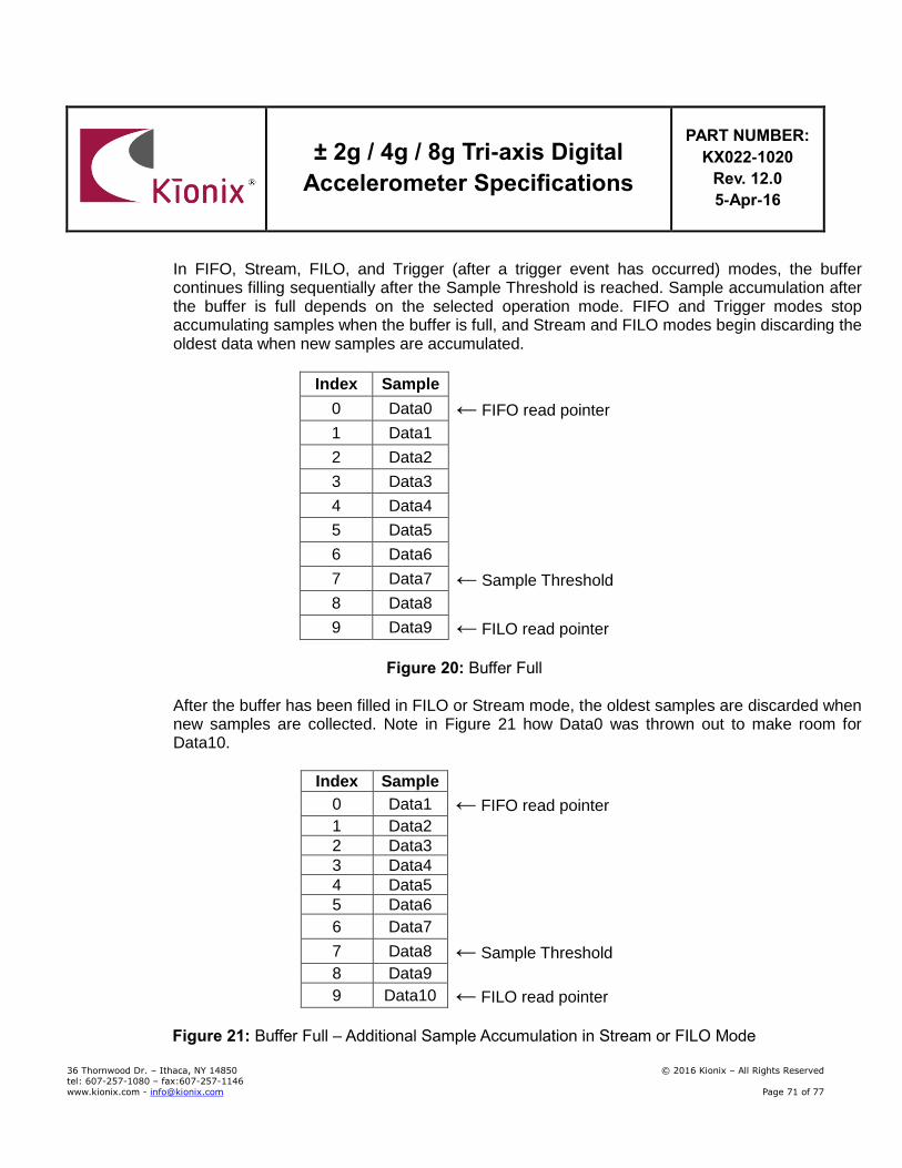
± 2g / 4g / 8g Tri-axis Digital
Accelerometer Specifications
PART NUMBER:
KX022-1020
Rev. 12.0
5-Apr-16
36 Thornwood Dr. – Ithaca, NY 14850 © 2016 Kionix – All Rights Reserved tel: 607-257-1080 – fax:607-257-1146
www.kionix.com - [email protected] Page 71 of 77
In FIFO, Stream, FILO, and Trigger (after a trigger event has occurred) modes, the buffer continues filling sequentially after the Sample Threshold is reached. Sample accumulation after the buffer is full depends on the selected operation mode. FIFO and Trigger modes stop accumulating samples when the buffer is full, and Stream and FILO modes begin discarding the oldest data when new samples are accumulated.
Index Sample
0 Data0 ← FIFO read pointer 1 Data1
2 Data2
3 Data3
4 Data4
5 Data5
6 Data6
7 Data7 ← Sample Threshold 8 Data8
9 Data9 ← FILO read pointer
Figure 20: Buffer Full
After the buffer has been filled in FILO or Stream mode, the oldest samples are discarded when new samples are collected. Note in Figure 21 how Data0 was thrown out to make room for Data10.
Index Sample
0 Data1 ← FIFO read pointer 1 Data2
2 Data3
3 Data4
4 Data5
5 Data6
6 Data7
7 Data8 ← Sample Threshold 8 Data9
9 Data10 ← FILO read pointer
Figure 21: Buffer Full – Additional Sample Accumulation in Stream or FILO Mode
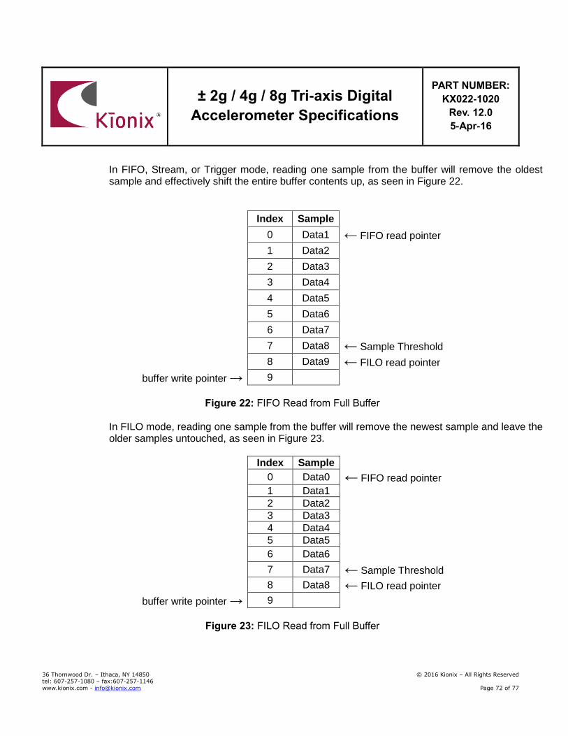
± 2g / 4g / 8g Tri-axis Digital
Accelerometer Specifications
PART NUMBER:
KX022-1020
Rev. 12.0
5-Apr-16
36 Thornwood Dr. – Ithaca, NY 14850 © 2016 Kionix – All Rights Reserved tel: 607-257-1080 – fax:607-257-1146
www.kionix.com - [email protected] Page 72 of 77
In FIFO, Stream, or Trigger mode, reading one sample from the buffer will remove the oldest sample and effectively shift the entire buffer contents up, as seen in Figure 22.
Index Sample
0 Data1 ← FIFO read pointer 1 Data2
2 Data3
3 Data4
4 Data5
5 Data6
6 Data7
7 Data8 ← Sample Threshold 8 Data9 ← FILO read pointer
buffer write pointer → 9
Figure 22: FIFO Read from Full Buffer
In FILO mode, reading one sample from the buffer will remove the newest sample and leave the older samples untouched, as seen in Figure 23.
Index Sample
0 Data0 ← FIFO read pointer 1 Data1
2 Data2
3 Data3
4 Data4
5 Data5
6 Data6
7 Data7 ← Sample Threshold 8 Data8 ← FILO read pointer
buffer write pointer → 9
Figure 23: FILO Read from Full Buffer
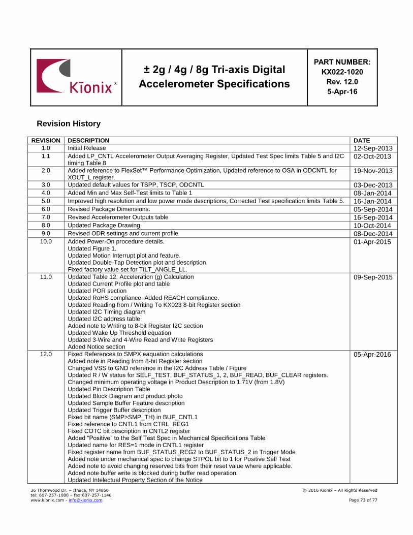
± 2g / 4g / 8g Tri-axis Digital
Accelerometer Specifications
PART NUMBER:
KX022-1020
Rev. 12.0
5-Apr-16
36 Thornwood Dr. – Ithaca, NY 14850 © 2016 Kionix – All Rights Reserved tel: 607-257-1080 – fax:607-257-1146
www.kionix.com - [email protected] Page 73 of 77
Revision History REVISION DESCRIPTION DATE
1.0 Initial Release 12-Sep-2013 1.1 Added LP_CNTL Accelerometer Output Averaging Register, Updated Test Spec limits Table 5 and I2C
timing Table 8 02-Oct-2013
2.0 Added reference to FlexSet™ Performance Optimization, Updated reference to OSA in ODCNTL for XOUT_L register.
19-Nov-2013
3.0 Updated default values for TSPP, TSCP, ODCNTL 03-Dec-2013 4.0 Added Min and Max Self-Test limits to Table 1 08-Jan-2014 5.0 Improved high resolution and low power mode descriptions, Corrected Test specification limits Table 5. 16-Jan-2014 6.0 Revised Package Dimensions. 05-Sep-2014 7.0 Revised Accelerometer Outputs table 16-Sep-2014 8.0 Updated Package Drawing 10-Oct-2014 9.0 Revised ODR settings and current profile 08-Dec-2014
10.0 Added Power-On procedure details. Updated Figure 1. Updated Motion Interrupt plot and feature. Updated Double-Tap Detection plot and description. Fixed factory value set for TILT_ANGLE_LL.
01-Apr-2015
11.0 Updated Table 12: Acceleration (g) Calculation Updated Current Profile plot and table Updated POR section Updated RoHS compliance. Added REACH compliance. Updated Reading from / Writing To KX023 8-bit Register section Updated I2C Timing diagram Updated I2C address table Added note to Writing to 8-bit Register I2C section Updated Wake Up Threshold equation Updated 3-Wire and 4-Wire Read and Write Registers Added Notice section
09-Sep-2015
12.0 Fixed References to SMPX eaquation calculations Added note in Reading from 8-bit Register section Changed VSS to GND reference in the I2C Address Table / Figure Updated R / W status for SELF_TEST, BUF_STATUS_1, 2, BUF_READ, BUF_CLEAR registers. Changed minimum operating voltage in Product Description to 1.71V (from 1.8V) Updated Pin Description Table Updated Block Diagram and product photo Updated Sample Buffer Feature description Updated Trigger Buffer description Fixed bit name (SMP>SMP_TH) in BUF_CNTL1 Fixed reference to CNTL1 from CTRL_REG1 Fixed COTC bit description in CNTL2 register Added “Positive” to the Self Test Spec in Mechanical Specifications Table Updated name for RES=1 mode in CNTL1 register Fixed register name from BUF_STATUS_REG2 to BUF_STATUS_2 in Trigger Mode Added note under mechanical spec to change STPOL bit to 1 for Positive Self Test Added note to avoid changing reserved bits from their reset value where applicable. Added note buffer write is blocked during buffer read operation. Updated Intelectual Property Section of the Notice
05-Apr-2016
± 2g / 4g / 8g Tri-axis Digital
Accelerometer Specifications
PART NUMBER:
KX022-1020
Rev. 12.0
5-Apr-16
36 Thornwood Dr. – Ithaca, NY 14850 © 2016 Kionix – All Rights Reserved tel: 607-257-1080 – fax:607-257-1146
www.kionix.com - [email protected] Page 74 of 77
"Kionix" is a registered trademark of Kionix, Inc. Products described herein are protected by patents issued or pending. No license is granted by implication or otherwise under any patent or other rights of Kionix. The information contained herein is believed to be accurate and reliable but is not guaranteed. Kionix does not assume responsibility for its use or distribution. Kionix also reserves the right to change product specifications or discontinue this product at any time without prior notice. This publication supersedes and replaces all information previously supplied.
± 2g / 4g / 8g Tri-axis Digital
Accelerometer Specifications
PART NUMBER:
KX022-1020
Rev. 12.0
5-Apr-16
36 Thornwood Dr. – Ithaca, NY 14850 © 2016 Kionix – All Rights Reserved tel: 607-257-1080 – fax:607-257-1146
www.kionix.com - [email protected] Page 75 of 77
Notice
Precaution on using KIONIX Products 1. Our Products are designed and manufactured for application in ordinary electronic equipment (such as AV
equipment, OA equipment, telecommunication equipment, home electronic appliances, amusement equipment, etc.). If you intend to use our Products in devices requiring extremely high reliability (such as medical equipment (Note 1), transport equipment, traffic equipment, aircraft/spacecraft, nuclear power controllers, fuel controllers, car equipment including car accessories, safety devices, etc.) and whose malfunction or failure may cause loss of human life, bodily injury or serious damage to property (“Specific Applications”), please consult with the KIONIX sales representative in advance. Unless otherwise agreed in writing by KIONIX in advance, KIONIX shall not be in any way responsible or liable for any damages, expenses or losses incurred by you or third parties arising from the use of any KIONIX’s Products for Specific Applications.
(Note1) Medical Equipment Classification of the Specific Applications
JAPAN USA EU CHINA
CLASSⅢ CLASSⅢ
CLASSⅡb CLASSⅢ
CLASSⅣ CLASSⅢ
2. KIONIX designs and manufactures its Products subject to strict quality control system. However, semiconductor
products can fail or malfunction at a certain rate. Please be sure to implement, at your own responsibilities, adequate safety measures including but not limited to fail-safe design against the physical injury, damage to any property, which a failure or malfunction of our Products may cause. The following are examples of safety measures: a) Installation of protection circuits or other protective devices to improve system safety b) Installation of redundant circuits to reduce the impact of single or multiple circuit failure
3. Our Products are designed and manufactured for use under standard conditions and not under any special or extraordinary environments or conditions, as exemplified below. Accordingly, KIONIX shall not be in any way responsible or liable for any damages, expenses or losses arising from the use of any KIONIX’s Products under any special or extraordinary environments or conditions. If you intend to use our Products under any special or extraordinary environments or conditions (as exemplified below), your independent verification and confirmation of product performance, reliability, etc., prior to use, must be necessary: a) Use of our Products in any types of liquid, including water, oils, chemicals, and organic solvents b) Use of our Products outdoors or in places where the Products are exposed to direct sunlight or dust c) Use of our Products in places where the Products are exposed to sea wind or corrosive gases, including Cl2,
H2S, NH3, SO2, and NO2 d) Use of our Products in places where the Products are exposed to static electricity or electromagnetic waves e) Use of our Products in proximity to heat-producing components, plastic cords, or other flammable items f) Sealing or coating our Products with resin or other coating materials g) Use of our Products without cleaning residue of flux (even if you use no-clean type fluxes, cleaning residue of
flux is recommended); or Washing our Products by using water or water-soluble cleaning agents for cleaning residue after soldering
h) Use of the Products in places subject to dew condensation 4. The Products are not subject to radiation-proof design. 5. Please verify and confirm characteristics of the final or mounted products in using the Products. 6. In particular, if a transient load (a large amount of load applied in a short period of time, such as pulse. is applied,
confirmation of performance characteristics after on-board mounting is strongly recommended. Avoid applying

± 2g / 4g / 8g Tri-axis Digital
Accelerometer Specifications
PART NUMBER:
KX022-1020
Rev. 12.0
5-Apr-16
36 Thornwood Dr. – Ithaca, NY 14850 © 2016 Kionix – All Rights Reserved tel: 607-257-1080 – fax:607-257-1146
www.kionix.com - [email protected] Page 76 of 77
power exceeding normal rated power; exceeding the power rating under steady-state loading condition may negatively affect product performance and reliability.
7. De-rate Power Dissipation (Pd) depending on ambient temperature (Ta). When used in sealed area, confirm the actual ambient temperature.
8. Confirm that operation temperature is within the specified range described in the product specification. 9. KIONIX shall not be in any way responsible or liable for failure induced under deviant condition from what is
defined in this document.
Precaution for Mounting / Circuit board design 1. When a highly active halogenous (chlorine, bromine, etc.) flux is used, the residue of flux may negatively affect
product performance and reliability. 2. In principle, the reflow soldering method must be used; if flow soldering method is preferred, please consult with
the KIONIX representative in advance. For details, please refer to KIONIX Mounting specification.
Precautions Regarding Application Examples and External Circuits 1. If change is made to the constant of an external circuit, please allow a sufficient margin considering variations of
the characteristics of the Products and external components, including transient characteristics, as well as static characteristics.
2. You agree that application notes, reference designs, and associated data and information contained in this document are presented only as guidance for Products use. Therefore, in case you use such information, you are solely responsible for it and you must exercise your own independent verification and judgment in the use of such information contained in this document. KIONIX shall not be in any way responsible or liable for any damages, expenses or losses incurred by you or third parties arising from the use of such information.
Precaution for Electrostatic This Product is electrostatic sensitive product, which may be damaged due to electrostatic discharge. Please take proper caution in your manufacturing process and storage so that voltage exceeding the Products maximum rating will not be applied to Products. Please take special care under dry condition (e.g. Grounding of human body / equipment / solder iron, isolation from charged objects, setting of Ionizer, friction prevention and temperature / humidity control).
Precaution for Storage / Transportation 1. Product performance and soldered connections may deteriorate if the Products are stored in the places where:
a) the Products are exposed to sea winds or corrosive gases, including Cl2, H2S, NH3, SO2, and NO2 b) the temperature or humidity exceeds those recommended by KIONIX c) the Products are exposed to direct sunshine or condensation d) the Products are exposed to high Electrostatic
2. Even under KIONIX recommended storage condition, solderability of products out of recommended storage time period may be degraded. It is strongly recommended to confirm solderability before using Products of which storage time is exceeding the recommended storage time period.
3. Store / transport cartons in the correct direction, which is indicated on a carton with a symbol. Otherwise bent leads may occur due to excessive stress applied when dropping of a carton.
4. Use Products within the specified time after opening a humidity barrier bag. Baking is required before using Products of which storage time is exceeding the recommended storage time period.

± 2g / 4g / 8g Tri-axis Digital
Accelerometer Specifications
PART NUMBER:
KX022-1020
Rev. 12.0
5-Apr-16
36 Thornwood Dr. – Ithaca, NY 14850 © 2016 Kionix – All Rights Reserved tel: 607-257-1080 – fax:607-257-1146
www.kionix.com - [email protected] Page 77 of 77
Precaution for Product Label QR code printed on KIONIX Products label is for KIONIX’s internal use only.
Precaution for Disposition When disposing Products please dispose them properly using an authorized industry waste company.
Precaution for Foreign Exchange and Foreign Trade act Since our Products might fall under controlled goods prescribed by the applicable foreign exchange and foreign trade act, please consult with KIONIX representative in case of export.
Precaution Regarding Intellectual Property Rights 1. All information and data including but not limited to application example contained in this document is for
reference only. KIONIX does not warrant that foregoing information or data will not infringe any intellectual property rights or any other rights of any third party regarding such information or data.
2. KIONIX shall not be in any way responsible or liable for infringement of any intellectual property rights or other damages arising from use of such information or data.
3. No license, expressly or implied, is granted hereby under any intellectual property rights or other rights of KIONIX or any third parties with respect to the Products or the information contained in this document. Provided, however, that KIONIX will not assert its intellectual property rights or other rights against you or your customers to the extent necessary to manufacture or sell products containing the Products, subject to the terms and conditions herein.
Other Precaution 1. This document may not be reprinted or reproduced, in whole or in part, without prior written consent of KIONIX. 2. The Products may not be disassembled, converted, modified, reproduced or otherwise changed without prior
written consent of KIONIX. 3. In no event shall you use in any way whatsoever the Products and the related technical information contained in
the Products or this document for any military purposes, including but not limited to, the development of mass-destruction weapons.
4. The proper names of companies or products described in this document are trademarks or registered trademarks of KIONIX, its affiliated companies or third parties.
General Precaution 1. Before you use our Products, you are requested to carefully read this document and fully understand its contents.
KIONIX shall not be in any way responsible or liable for failure, malfunction or accident arising from the use of any KIONIX’s Products against warning, caution or note contained in this document.
2. All information contained in this document is current as of the issuing date and subject to change without any prior notice. Before purchasing or using KIONIX’s Products, please confirm the latest information with a KIONIX sales representative.
3. The information contained in this document is provided on an “as is” basis and KIONIX does not warrant that all information contained in this document is accurate and/or error-free. KIONIX shall not be in any way responsible or liable for any damages, expenses or losses incurred by you or third parties resulting from inaccuracy or errors of or concerning such information.