Embed Size (px)
Citation preview

Molecular Beam Epitaxy of 2D Chalcogenides: Challenges & Opportunities
Nitin SamarthDept. of Physics
Penn State

Outline
Overview of 2DCC goals & facilities Chalcogenides: what are the materials of interest and why? Molecular beam epitaxy (MBE) of Bi- and Sb-chalcogenide topological
insulators: status of field MBE of transition metal dichalcogenides: status of field MBE of superconducting chalcogenides: status of field The 2DCC platform: MBE capabilities, current & future

2D monolayers, surfaces and interfaces of chalcogenides are emerging as a compelling class of systems with transformative new science that can be harnessed for novel device technologies.
2D Materials for Next Generation Electronics
TIs & TMDs: steep slope transistors
(< 60 mV/decade)
Topological spintronics: efficient spin transfer torque for
low power MRAM (fJ/switch)
Mellnik et al., Nature 511, 449 (2014)
Lin et al., Nature Comm. 6, 7311 (2015)
Hybrid 2D devices
Fiori et al., Nature Nano. 9, 768 (2014)

Overview of 2DCC Platform
Develop custom deposition tools with in situ and real time characterization of monolayer and few layer films.
Unique capabilities in simulation of reaction kinetics through first principles + reactive potential approach

Wide range of growth strategies utilizing low energy deposition techniques
chemical vapor
deposition
physical vapor
deposition
MOCVD Solid source MBE
CBE / MOMBEhybrid MBE

• Develop the science of 2D chalcogenide “epitaxy” to match level of established material systems such as III-V, II-VI, IV, oxides, Heuslers.
• Enable wafer scale growth of ‘electronic grade’ single layers and heterostructures.• Develop new growth approaches, deposition tools and techniques to enable atomic
level control and understanding of wafer-scale synthesis.• Utilize theory/simulation tools to gain insight into growth processes and guide
exploration of the multidimensional growth parameter space.• Use improvements in thin film growth to make influential scientific discoveries and
technological advances.
Scientific Goals of MBE Effort in 2DCC
Advances in synthesis are needed to drive further developments in the field.

• Chalcogenide ‘topological insulators’: Bi2Se3, Bi2Te3, Sb2Te3.
• Transition metal dichalcogenides (TMDs): WTe2, MoTe2, WSe2, MoSe2,NbSe2
• Transition metal monochalcogenide superconductors: FeSe, FeTe
• Magnetic doping of host Bi- and Sb-chalcogenides
Materials of immediate interest
Focus on '2D chalcogenides' in a broad sense: monolayers, surfaces, ultrathin limit etc.
• Spin-orbit coupling + symmetry leads to 2D ‘helical Dirac fermions’ on surfaces of Bi2Se3, Bi2Te3, Sb2Te3 (and their alloys): ‘3D topological insulators.’
• ‘Spin-momentum locking’ of 2D helical Dirac surface states: spintronic devices.• ’Exotic broken symmetry surface states’:
– Interfacing with magnetism creates dissipation-less edge transport in quantum anomalous Hall insulator.
– Interfacing with superconductivity could lead to Majorana fermions for fault tolerant quantum computation.
Topological Insulators: 2D Surface States
H. Zhang, C.-X. Liu, et al., Nature Physics 5, 438 (2009)Fu & Kane, Phys. Rev. B 76, 045302 (2007)Moore & Balents, Phys. Rev. B 75, 121306(R) (2007)Roy, Phys. Rev. B 79, 195321 (2009)

Existing MBE Capabilities in 2DCC
Existing chalcogenide MBE capability available for 2DCC sample request proposals.
Chalcogenide MBE: thin films of Bi2Se3, Bi2Te3, (Bi,Sb)2Te3 on GaAs (111), InP (111), SrTiO3 (111), sapphire (0001).Also demonstrated growth on hBN, graphene, NbSe2, BSSCO, YIG.
Topological insulators + magnetism or superconductivity.Wang et al. Phys. Rev. Lett. 117, 076601 (2016).Liu et al., Science Advances. 2, 1600167 (2016).Lachman et al. Science Advances 1, e1500740 (2015).Kandala et al., Nature Comm. 6, 7434 (2015).Mellnik et al., Nature 511, 449 (2014).Xu et al., Nature Phys. 10, 943 (2014).Xu et al., Nature Phys. 8, 616 (2012).

Substrates for Bi- & Sb-chalcogenides
Conventional lattice matching constraints to the substrate are relaxed significantlyIn Van der Waals bonded materials.
Material “a” lattice constant “c” lattice constant
Bi2Se3 0.414 nm 1 QL = 0.9515 nm
Bi2Te3 0.438 nm 1 QL = 1.012 nm
Sb2Te3 0.426 nm 1 QL = 1.015 nm
Substrate Material “a” lattice constant
In-plane Mismatchof Bi2Se3
In-plane Mismatchof Bi2Te3
GaAs (111) 0.400 nm 3.54 % compressive
9.65 % compressive
InP (111) 0.415 nm 0.24 % tensile 5.65 % compressive
Sapphire 0.475 nm 15.8 % tensile 7.72 % tensile
SrTiO3 0.552 nm 25.0 % tensile 20.6 % tensile

Substrates for Bi- & Sb-chalcogenides
Conventional lattice matching constraints to the substrate are relaxed significantlyin Van der Waals bonded materials. But interface chemistry likely matters!
Substrate Material “a” lattice constant
In-plane Mismatchof Bi2Se3
In-plane Mismatchof Bi2Te3
GaAs (111) 0.400 nm 3.54 % compressive
9.65 % compressive
InP (111) 0.415 nm 0.24 % tensile 5.65 % compressive
Sapphire 0.475 nm 15.8 % tensile 7.72 % tensile
SrTiO3 0.552 nm 25.0 % tensile 20.6 % tensile
Bi2Se3 on saphhire; Bansal et al., Phys. Rev. Lett. 109, 116804 (2012) [S. Oh, Rutgers]
Bi2Se3 on InP (111); Richardella et al., APLMat. 3, 083303 (2015)

• Coherent Van der Waals epitaxy of Bi- and Sb-chalcogenides demonstrated on variety of substrates (InP, GaAs, SrTiO3, sapphire) by many groups.
• Lattice mismatch with substrate not a critical consideration but defects abound: textured surfaces, twins, small grain sizes ~200 nm), extrinsic doping (vacancies).
MBE of Bi- and Sb-chalcogenides: status of field
Epitaxy of Bi- and Sb- chalcogenides is still immature, compared to III-Vs
(Bi,Cr,Sb)2Te3 on InP (111)APL Mat. 3, 083303 (2015)
Desorbed under As-flux Desorbed under Se-flux

• Complex films and heterostructures can be grown on variety of substrates: e.g. Cr-, V-doped (Bi,Sb)2Te3 on InP (111), STO (111)
• Defects such as twinning are again often present, with corresponding tilted domains. • Microscopic nature of incorporation of magnetic dopants (e.g. Cr, V, Mn) varies with
details: substitutional vs interstitial; random vs. clustered.
MBE of Bi- and Sb-chalcogenides: status of field
Epitaxy of TI chalcogenides is advanced, yet quite immature compared to III-Vs
(Bi,Cr,Sb)2Te3 on InP (111)APL Mat. 3, 083303 (2015)

• Complex films and heterostructures can be grown on variety of substrates: e.g. Cr-, V-doped (Bi,Sb)2Te3 on InP (111), STO (111)
• Incorporation of some magnetic dopants (e.g. Cr) appears to be uniform
MBE of Bi- and Sb-chalcogenides: status of field
Epitaxy of TI chalcogenides is advanced, yet quite immature compared to III-Vs
(Bi,Sb,Cr)2Te3 on InP (111)
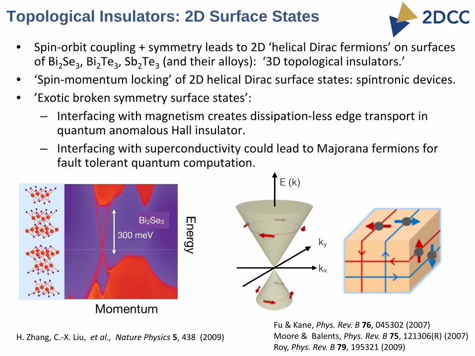
• Spin- and angle-resolved photoemission spectroscopy (ARPES) provides direct probe of helical Dirac fermions on surfaces.
• Ultrathin films: quantum engineering of surface states (hybridization) provides control over spin polarization & Dirac cone
Topological Insulators: ARPES probe of surface
Neupane, Richardella et al., Nature Communications 5, 3841 (2014)
How precisely can we control ultrathin films?
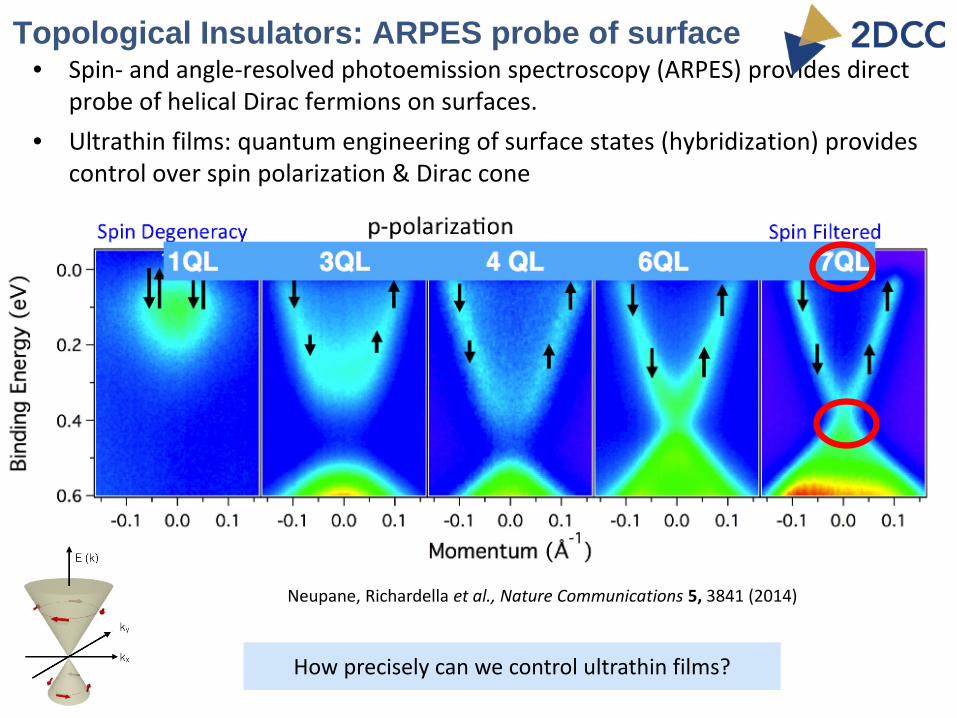
Topological Insulators: Exotic Quantum States
Chang et al., Science 340, 167 (2013).Chang, et al., Nature Materials 14, 473 (2015)
Broken time reversal symmetry in magnetically-doped topological insulators creates dissipation-less edge transport and precisely quantized Hall resistance.
‘Quantum anomalous Hall insulator’
How do we enhance the temperature at which these
exotic phenomena are observed?

• Even the `best’ (Bi,Sb,Cr)2Te3 films are highly disordered: double crystal rocking curves of 0.10 and electron mobility of a few hundred cm2/V.s
• Yet, quantum anomalous Hall effect is precisely quantized (4 parts in 104) and sheet resistance is small (a few ohms)
MBE of Bi- and Sb-chalcogenides: status of field
How will quantum properties evolve as disorder is reduced?
Liu et al., Science Advances. 2, (2016)

MBE of Bi- and Sb-chalcogenides: status of field
Clever development of engineered buffer layers is critical to advancing crystal quality
Record mobility (about 1.5 x 104 cm2/V.s)Observation of integer quantum Hall effect
Koirala et al., Nano Lett. 15, 8245 (2015) [S. Oh, Rutgers]

MBE growth of TMDs is still in its infancy, but…
MBE of HfSe2 on HOPG & MoS2Yue et al., ACS Nano 9, 474 (2015)
(Hinkle, UT Dallas)
MBE of TMDs: status of field
Challenges & opportunities:Need to understand nucleation & role of substrate.In-situ real time probes and in vacuocharacterization in conjunction with atomic scale simulation to provide insights into growth process and enables rapid improvements.
• Until recently only few reports on selected TMDs (MoTe2, MoSe2, WSe2, HfSe2)
• Structural quality is unclear from available publications.
• Grain sizes seem to be very small (< 100 nm).

MBE growth of TMDs is at its infancy stage, but rapidly progressing!
• Until recently only few reports on selected TMDs (MoTe2, MoSe2, WSe2, HfSe2)
• Structural quality is unclear from available publications.
• Grain sizes seem to be very small (< 100 nm).
MBE of MoTe2 on c-Al2O3 (0001)Arxiv:1603.02656
(Tutuc & Bannerjee, UT-Austin)
MBE of TMDs: status of field
Challenges & opportunities:Need to understand nucleation & role of substrate.In-situ real time probes and in vacuocharacterization in conjunction with atomic scale simulation to provide insights into growth process and enables rapid improvements.

Challenges & opportunities:MBE growth of a variety of chalcogenideheterostructures & superlattices recently demonstrated: MoSe2/MoTe2, Bi2Se3/MoSe2, Bi2Te3/MoTe2, Bi2Se3/MoSe2, etc.How to improve structural quality?
MBE growth of TMD superlattices is promising.
S. Vishwanath et al., “Controllable growth of layered selenide and telluride heterostructures & superlattices by MBE,” J. Mater. Res. 31, 900 (2016)(Cornell, Notre Dame)
MBE of TMDs: status of field

Challenges & opportunities:• Reproducibility of high TC• Ex situ observation of high TC• Diamagnetism: No proof yet• Mechanism: What determines
TC? What are upper limits? Why interface with STO?
MBE of transition metal monochalcogenides: status
MBE growth of ultrathin FeSe presents exciting new opportunities and unresolved questions in superconductivity
“Superconductivity above 100K in single layer FeSe films on doped STO,” Ge et al., Nature Materials 14, 285 (2015).

MBE #1: Expanding Growth Capabilities
2017: multiple in vacuo transfer options to broaden the user community and ensure full compatibility of growth and characterization capabilities
sputter system(oxides/metals)
hybrid oxide MBE
load lock
hybrid chalcogenide MBE
(2017)UHV
vacuum shuttle
Source: SAES
(Engel-Herbert)
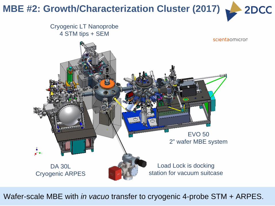
MBE #2: Growth/Characterization Cluster (2017)
Wafer-scale MBE with in vacuo transfer to cryogenic 4-probe STM + ARPES.
EVO 502” wafer MBE system
DA 30LCryogenic ARPES
Cryogenic LT Nanoprobe4 STM tips + SEM
Load Lock is docking station for vacuum suitcase

MBE #2: thin film growth
Initial focus on solid source MBE.
EVO 502” wafer MBE system Specifications:
o 2” substrate capabilityo Adaptor for smaller 1 cm2 substrates
for use in STM + ARPES
o Se crackero 6 pocket e-gun source for transition
metals (Fe, Nb, V, W, Mo, EuS)o effusion cells for Te, Bi, Cr, Sb, Fe
o KSA BandIT for substrate temperature and control
o base pressure 1×10⁻¹⁰ Torro turbo pump and ion pump

MBE #2: STM & transport
In vacuo transfer to cryogenic four probe STM for temperature-dependent resistivity + single tip spectroscopy
Cryogenic STM & four probe:
Four independent scanning probe microscopy tips
Orsay Vortex SEM column and detector for guiding and positioning of tips
Base sample temperature < 5 K for at least 36 hours
Superconducting coil ~ 200 Oe
Cryogenic LT Nanoprobe4 STM tips + SEM

MBE #2: ARPES
In vacuo transfer to cryogenic ARPES provides access to band structure
DA 30LCryogenic ARPES
Cryogenic ARPES:
High intensity, narrow line width He UV light source
Compact monochromator optimized for He I and He II
Energy resolution 1.8 meV at 2 eV pass energy, 20 eV kinetic energy
Angular mode energy range: 3 eV – 1.5 keV Upgradeable to include spin resolved detector Base sample temperature < 20 K
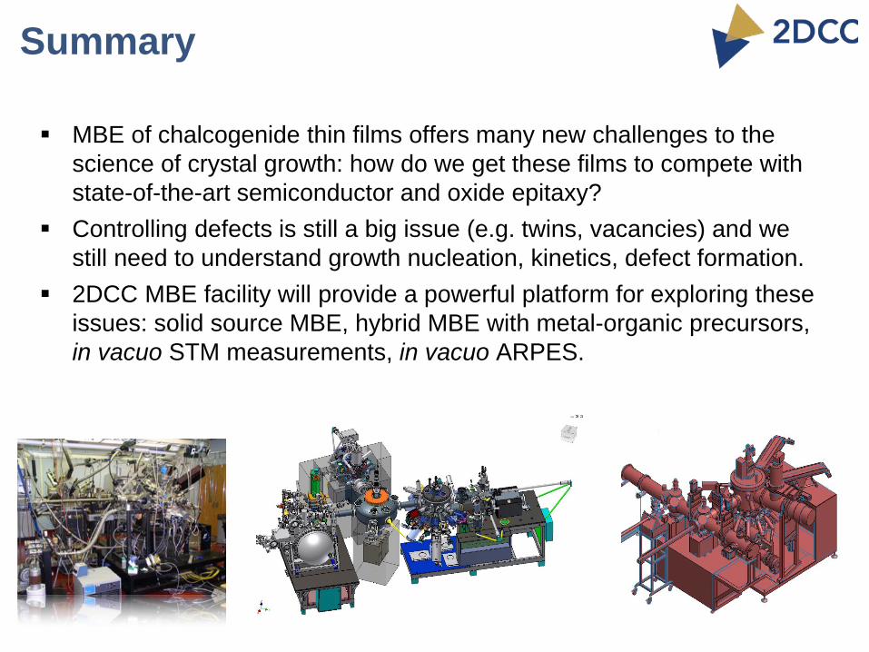
Summary
MBE of chalcogenide thin films offers many new challenges to the science of crystal growth: how do we get these films to compete with state-of-the-art semiconductor and oxide epitaxy?
Controlling defects is still a big issue (e.g. twins, vacancies) and we still need to understand growth nucleation, kinetics, defect formation.
2DCC MBE facility will provide a powerful platform for exploring these issues: solid source MBE, hybrid MBE with metal-organic precursors, in vacuo STM measurements, in vacuo ARPES.


![Consortium for Materials Properties Research in Earth Sciences Funded by NSF Division of Earth Sciences [2002-2012] Presentation to Electorate by Bob Liebermann](https://img.pdfslide.us/doc/110x75/56649f165503460f94c2bf5e/consortium-for-materials-properties-research-in-earth-sciences-funded-by-nsf.jpg)