Embed Size (px)
Citation preview

*Other brands and names are the property of their respective owners.Information in this document is provided in connection with Intel products. Intel assumes no liability whatsoever, including infringement of any patent orcopyright, for sale and use of Intel products except as provided in Intel’s Terms and Conditions of Sale for such products. Intel retains the right to makechanges to these specifications at any time, without notice. Microcomputer Products may have minor variations to this specification known as errata.
November 1994COPYRIGHT © INTEL CORPORATION, 1995 Order Number: 290204-008
28F512512K (64K x 8) CMOS FLASH MEMORY
Y Flash Electrical Chip-EraseÐ 1 Second Typical Chip-Erase
Y Quick-Pulse Programming AlgorithmÐ 10 ms Typical Byte-ProgramÐ 1 Second Chip-Program
Y 100,000 Erase/Program Cycles
Y 12.0V g5% VPP
Y High-Performance ReadÐ 120 ns Maximum Access Time
Y CMOS Low Power ConsumptionÐ 10 mA Typical Active CurrentÐ 50 mA Typical Standby CurrentÐ 0W Data Retention Power
Y Integrated Program/Erase Stop Timers
Y Command Register Architecture forMicroprocessor/MicrocontrollerCompatible Write Interface
Y Noise Immunity FeaturesÐ g10% VCC ToleranceÐ Maximum Latch-Up Immunity
through EPI Processing
Y ETOX II Nonvolatile Flash TechnologyÐ EPROM-Compatible Process BaseÐ High-Volume Manufacturing
Experience
Y JEDEC-Standard PinoutsÐ 32-Pin Plastic DipÐ 32-Lead PLCC(See Packaging Spec., Order Ý231369)
Y Extended Temperature Options
Intel’s 28F512 CMOS flash memory offers the most cost-effective and reliable alternative for read/writerandom access nonvolatile memory. The 28F512 adds electrical chip-erasure and reprogramming to familiarEPROM technology. Memory contents can be rewritten: in a test socket; in a PROM-programmer socket; on-board during subassembly test; in-system during final test; and in-system after-sale. The 28F512 increasesmemory flexibility, while contributing to time- and cost-savings.
The 28F512 is a 512-kilobit nonvolatile memory organized as 65,536 bytes of 8 bits. Intel’s 28F512 is offeredin 32-pin plastic dip or 32-lead PLCC packages. Pin assignments conform to JEDEC standards for byte-wideEPROMs.
Extended erase and program cycling capability is designed into Intel’s ETOX II (EPROM Tunnel Oxide) pro-cess technology. Advanced oxide processing, an optimized tunneling structure, and lower electric field com-bine to extend reliable cycling beyond that of traditional EEPROMs. With the 12.0V VPP supply, the 28F512performs 100,000 erase and program cycles well within the time limits of the Quick-Pulse Programming andQuick-Erase algorithms.
Intel’s 28F512 employs advanced CMOS circuitry for systems requiring high-performance access speeds, lowpower consumption, and immunity to noise. Its 120 nanosecond access time provides no-WAIT-state perform-ance for a wide range of microprocessors and microcontrollers. Maximum standby current of 100 mA trans-lates into power savings when the device is deselected. Finally, the highest degree of latch-up protection isachieved through Intel’s unique EPI processing. Prevention of latch-up is provided for stresses up to 100 mAon address and data pins, from b1V to VCC a 1V.
With Intel’s ETOX II process base, the 28F512 levers years of EPROM experience to yield the highest levels ofquality, reliability, and cost-effectiveness.

28F512
290204–1
Figure 1. 28F512 Block Diagram
2
28F512
290204–2
290204–3
Graphic Not to Scale
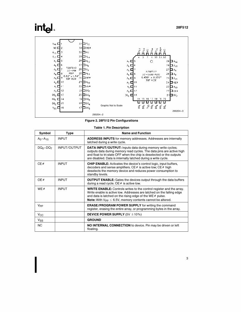
Figure 2. 28F512 Pin Configurations
Table 1. Pin Description
Symbol Type Name and Function
A0–A15 INPUT ADDRESS INPUTS for memory addresses. Addresses are internallylatched during a write cycle.
DQ0–DQ7 INPUT/OUTPUT DATA INPUT/OUTPUT: Inputs data during memory write cycles;outputs data during memory read cycles. The data pins are active highand float to tri-state OFF when the chip is deselected or the outputsare disabled. Data is internally latched during a write cycle.
CEÝ INPUT CHIP ENABLE: Activates the device’s control logic, input buffers,decoders and sense amplifiers. CEÝ is active low; CEÝ highdeselects the memory device and reduces power consumption tostandby levels.
OEÝ INPUT OUTPUT ENABLE: Gates the devices output through the data buffersduring a read cycle. OEÝ is active low.
WEÝ INPUT WRITE ENABLE: Controls writes to the control register and the array.Write enable is active low. Addresses are latched on the falling edgeand data is latched on the rising edge of the WEÝ pulse.
Note: With VPP s 6.5V, memory contents cannot be altered.
VPP ERASE/PROGRAM POWER SUPPLY for writing the commandregister, erasing the entire array, or programming bytes in the array.
VCC DEVICE POWER SUPPLY (5V g10%)
VSS GROUND
NC NO INTERNAL CONNECTION to device. Pin may be driven or leftfloating.
3
28F512
APPLICATIONS
The 28F512 flash memory provides nonvolatilityalong with the capability to perform over 100,000electrical chip-erasure/reprogram cycles. These fea-tures make the 28F512 an innovative alternative todisk, EEPROM, and battery-backed static RAM.Where periodic updates of code and data-tables arerequired, the 28F512’s reprogrammability and non-volatility make it the obvious and ideal replacementfor EPROM.
Primary applications and operating systems storedin flash eliminate the slow disk-to-DRAM downloadprocess. This results in dramatic enhancement ofperformance and substantial reduction of powerconsumption Ð a consideration particularly impor-tant in portable equipment. Flash memory increasesflexibility with electrical chip erasure and in-systemupdate capability of operating systems and applica-tion code. With updatable BIOS, system manufactur-ers can easily accommodate last-minute changes asrevisions are made.
In diskless workstations and terminals, network traf-fic reduces to a minimum and systems are instant-on. Reliability exceeds that of electromechanicalmedia. Often in these environments, power interrup-tions force extended re-boot periods for all net-worked terminals. This mishap is no longer an issueif boot code, operating systems, communication pro-tocols and primary applications are flash-resident ineach terminal.
For embedded systems that rely on dynamic RAM/disk for main system memory or nonvolatile backupstorage, the 28F512 flash memory offers a solidstate alternative in a minimal form factor. The28F512 provides higher performance, lower powerconsumption, instant-on capability, and allows an‘‘execute in place’’ memory hierarchy for code anddata table reading. Additionally, the flash memory ismore rugged and reliable in harsh environmentswhere extreme temperatures and shock can causedisk-based systems to fail.
The need for code updates pervades all phases of asystem’s life Ð from prototyping to system manufac-ture to after-sale service. The electrical chip-erasureand reprogramming ability of the 28F512 allows in-
circuit alterability; this eliminates unnecessary han-dling and less-reliable socketed connections, whileadding greater test, manufacture, and update flexi-bility.
Material and labor costs associated with codechanges increases at higher levels of system inte-gration Ð the most costly being code updates aftersale. Code ‘‘bugs’’, or the desire to augment systemfunctionality, prompt after-sale code updates. Fieldrevisions to EPROM-based code requires the re-moval of EPROM components or entire boards. Withthe 28F512, code updates are implemented locallyvia an edge-connector, or remotely over a commun-cation link.
For systems currently using a high-density staticRAM/battery configuration for data accumulation,flash memory’s inherent nonvolatility eliminates theneed for battery backup. The concern for batteryfailure no longer exists, an important considerationfor portable equipment and medical instruments,both requiring continuous performance. In addition,flash memory offers a considerable cost advantageover static RAM.
Flash memory’s electrical chip erasure, byte pro-grammability and complete nonvolatility fit well withdata accumulation and recording needs. Electricalchip-erasure gives the designer a ‘‘blank slate’’ inwhich to log or record data. Data can be periodicallyoff-loaded for analysis and the flash memory erasedproducing a new ‘‘blank slate’’.
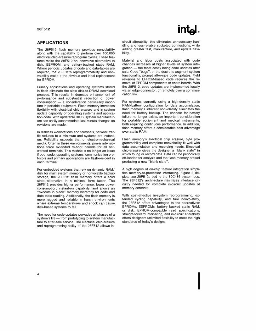
A high degree of on-chip feature integration simpli-fies memory-to-processor interfacing. Figure 3 de-picts two 28F512s tied to the 80C186 system bus.The 28F512’s architecture minimizes interface cir-cuitry needed for complete in-circuit updates ofmemory contents.
With cost-effective in-system reprogramming, ex-tended cycling capability, and true nonvolatility,the 28F512 offers advantages to the alternatives:EPROMs, EEPROMs, battery backed static RAM,or disk. EPROM-compatible read specifications,straight-forward interfacing, and in-circuit alterabilityoffers designers unlimited flexibility to meet the highstandards of today’s designs.
4
28F512
290204–5
Figure 3. 28F512 in a 80C186 System
PRINCIPLES OF OPERATION
Flash-memory augments EPROM functionality within-circuit electrical erasure and reprogramming. The28F512 introduces a command register to managethis new functionality. The command register allowsfor: 100% TTL-level control inputs; fixed power sup-plies during erasure and programming; and maxi-mum EPROM compatibility.
In the absence of high voltage on the VPP pin, the28F512 is a read-only memory. Manipulation of theexternal memory-control pins yields the standardEPROM read, standby, output disable, and Intelli-gent Identifier operations.
The same EPROM read, standby, and output disableoperations are available when high voltage is ap-plied to the VPP pin. In addition, high voltage on VPPenables erasure and programming of the device. Allfunctions associated with altering memory con-tentsÐIntelligent Identifier, erase, erase verify, pro-gram, and program verifyÐare accessed via thecommand register.
Commands are written to the register using standardmicroprocessor write timings. Register contentsserve as input to an internal state-machine whichcontrols the erase and programming circuitry. Writecycles also internally latch addresses and dataneeded for programming or erase operations. Withthe appropriate command written to the register,
standard microprocessor read timings output arraydata, access the Intelligent Identifier codes, or out-put data for erase and program verification.
Integrated Stop Timer
Successive command write cycles define the dura-tion of program and erase operations; specifically,the program or erase time durations are normallyterminated by associated program or erase verifycommands. An integrated stop timer provides simpli-fied timing control over these operations; thus elimi-nating the need for maximum program/erase timingspecifications. Programming and erase pulsedurations are minimums only. When the stop timerterminates a program or erase operation, the deviceenters an inactive state and remains inactive untilreceiving the appropriate verify or reset command.
Write Protection
The command register is only active when VPP is athigh voltage. Depending upon the application, thesystem designer may choose to make the VPP pow-er supply switchableÐavailable only when memoryupdates are desired. When VPP e VPPL, the con-tents of the register default to the read command,making the 28F512 a read-only memory. In thismode, the memory contents cannot be altered.
5

28F512
Table 2. 28F512 Bus Operations
PinsVPP
(1) A0 A9 CEÝ OEÝ WEÝ DQ0–DQ7Operation
Read VPPL A0 A9 VIL VIL VIH Data Out
Output Disable VPPL X X VIL VIH VIH Tri-State
READ-ONLY Standby VPPL X X VIH X X Tri-State
Intelligent Identifier (Mfr)(2) VPPL VIL VID(3) VIL VIL VIH Data e 89H
Intelligent Identifier (Device)(2) VPPL VIH VID(3) VIL VIL VIH Data e B8H
Read VPPH A0 A9 VIL VIL VIH Data Out(4)
READ/WRITEOutput Disable VPPH X X VIL VIH VIH Tri-State
Standby(5) VPPH X X VIH X X Tri-State
Write VPPH A0 A9 VIL VIH VIL Data In(6)
NOTES:1. Refer to DC Characteristics. When VPP e VPPL memory contents can be read but not written or erased.2. Manufacturer and device codes may also be accessed via a command register write sequence. Refer to Table 3. All otheraddresses low.3. VID is the Intelligent Identifier high voltage. Refer to DC Characteristics.4. Read operations with VPP e VPPH may access array data or the Intelligent Identifier codes.5. With VPP at high voltage, the standby current equals ICC a IPP (standby).6. Refer to Table 3 for valid Data-In during a write operation.7. X can be VIL or VIH.
Or, the system designer may choose to ‘‘hardwire’’VPP, making the high voltage supply constantlyavailable. In this case, all Command Register func-tions are inhibited whenever VCC is below the writelockout voltage VLK0. (See Power Up/Down Protec-tion). The 28F512 is designed to accommodate ei-ther design practice, and to encourage optimizationof the processor-memory interface.
The two-step program/erase write sequence to theCommand Register provides additional softwarewrite protection.
BUS OPERATIONS
Read
The 28F512 has two control functions, both of whichmust be logically active, to obtain data at the out-puts. Chip-Enable (CEÝ) is the power control andshould be used for device selection. Output-Enable(OEÝ) is the output control and should be usedto gate data from the output pins, independent ofdevice selection. Refer to AC read timingwaveforms.
When VPP is high (VPPH), the read operation can beused to access array data, to output the IntelligentIdentifier codes, and to access data for program/erase verification. When VPP is low (VPPL), the readoperation can only access the array data.
Output Disable
With Output-Enable at a logic-high level (VIH), outputfrom the device is disabled. Output pins are placedin a high-impedance state.
Standby
With Chip-Enable at a logic-high level, the standbyoperation disables most of the 28F512’s circuitryand substantially reduces device power consump-tion. The outputs are placed in a high-impedancestate, independent of the Output-Enable signal.If the 28F512 is deselected during erasure, pro-gramming, or program/erase verification, thedevice draws active current until the operation isterminated.
Intelligent Identifier Operation
The Intelligent Identifier operation outputs the manu-facturer code (89H) and device code (B8H). Pro-gramming equipment automatically matches the de-vice with its proper erase and programming algo-rithms.
6

28F512
With Chip-Enable and Output-Enable at a logic lowlevel, raising A9 to high voltage VID (see DC Charac-teristics) activates the operation. Data read from lo-cations 0000H and 0001H represent the manufac-turer’s code and the device code, respectively.
The manufacturer- and device-codes can also beread via the command register, for instances wherethe 28F512 is erased and reprogrammed in the tar-get system. Following a write of 90H to the com-mand register, a read from address location 0000Houtputs the manufacturer code (89H). A read fromaddress 0001H outputs the device code (B8H).
Write
Device erasure and programming are accomplishedvia the command register, when high voltage is ap-plied to the VPP pin. The contents of the registerserve as input to the internal state-machine. Thestate-machine outputs dictate the function of thedevice.
The command register itself does not occupy an ad-dressable memory location. The register is a latch
used to store the command, along with address anddata information needed to execute the command.
The command register is written by bringing Write-Enable to a logic-low level (VIL), while Chip-Enable islow. Addresses are latched on the falling edge ofWrite-Enable, while data is latched on the risingedge of the Write-Enable pulse. Standard microproc-essor write timings are used.
Refer to AC Write Characteristics and the Erase/Programming Waveforms for specific timingparameters.
COMMAND DEFINITIONS
When low voltage is applied to the VPP pin, the con-tents of the command register default to 00H, en-abling read-only operations.
Placing high voltage on the VPP pin enables read/write operations. Device operations are selected bywriting specific data patterns into the command reg-ister. Table 3 defines these 28F512 registercommands.
Table 3. Command Definitions
BusFirst Bus Cycle Second Bus Cycle
Command Cycles
Req’dOperation(1) Address(2) Data(3) Operation(1) Address(2) Data(3)
Read Memory 1 Write X 00H
Read Intelligent Identifier Code(4) 3 Write X 90H Read (4) (4)
Set-up Erase/Erase(5) 2 Write X 20H Write X 20H
Erase Verify(5) 2 Write EA A0H Read X EVD
Set-up Program/Program(6) 2 Write X 40H Write PA PD
Program Verify(6) 2 Write X C0H Read X PVD
Reset(7) 2 Write X FFH Write X FFH
NOTES:1. Bus operations are defined in Table 2.2. IA e Identifier address: 00H for manufacturer code, 01H for device code.
EA e Address of memory location to be read during erase verify.PA e Address of memory location to be programmed.Addresses are latched on the falling edge of the Write-Enable pulse.
3. ID e Data read from location IA during device identification (Mfr e 89H, Device e B8H).EVD e Data read from location EA during erase verify.PD e Data to be programmed at location PA. Data is latched on the rising edge of Write-Enable.PVD e Data read from location PA during program verify. PA is latched on the Program command.
4. Following the Read Intelligent ID command, two read operations access manufacturer and device codes.5. Figure 5 illustrates the Quick-Erase algorithm.6. Figure 4 illustrates the Quick-Pulse Programming algorithm.7. The second bus cycle must be followed by the desired command register write.
7

28F512
Read Command
While VPP is high, for erasure and programming,memory contents can be accessed via the readcommand. The read operation is initiated by writing00H into the command register. Microprocessorread cycles retrieve array data. The device remainsenabled for reads until the command register con-tents are altered.
The default contents of the register upon VPP pow-er-up is 00H. This default value ensures that no spu-rious alteration of memory contents occurs duringthe VPP power transition. Where the VPP supply ishard-wired to the 28F512, the device powers-up andremains enabled for reads until the command-regis-ter contents are changed. Refer to the AC ReadCharacteristics and Waveforms for specific timingparameters.
Intelligent Identifier Command
Flash-memories are intended for use in applicationswhere the local CPU alters memory contents. Assuch, manufacturer- and device-codes must be ac-cessible while the device resides in the target sys-tem. PROM programmers typically access signaturecodes by raising A9 to a high voltage. However, mul-tiplexing high voltage onto address lines is not a de-sired system-design practice.
The 28F512 contains an Intelligent Identifier opera-tion to supplement traditional PROM-programmingmethodology. The operation is initiated by writing90H into the command register. Following the com-mand write, a read cycle from address 0000H re-trieves the manufacturer code of 89H. A read cyclefrom address 0001H returns the device code ofB8H. To terminate the operation, it is necessary towrite another valid command into the register.
Set-up Erase/Erase Commands
Set-up Erase is a command-only operation thatstages the device for electrical erasure of all bytes inthe array. The set-up erase operation is performedby writing 20H to the command register.
To commence chip-erasure, the erase command(20H) must again be written to the register. Theerase operation begins with the rising edge of theWrite-Enable pulse and terminates with the risingedge of the next Write-Enable pulse (i.e., Erase-Veri-fy Command).
This two-step sequence of set-up followed by execu-tion ensures that memory contents are not acciden-tally erased. Also, chip-erasure can only occur whenhigh voltage is applied to the VPP pin. In the absence
of this high voltage, memory contents are protectedagainst erasure. Refer to AC Erase Characteristicsand Waveforms for specific timing parameters.
Erase-Verify Command
The erase command erases all bytes of the array inparallel. After each erase operation, all bytes mustbe verified. The erase verify operation is initiated bywriting A0H into the command register. The addressfor the byte to be verified must be supplied as it islatched on the falling edge of the Write-Enablepulse. The register write terminates the erase opera-tion with the rising edge of its Write-Enable pulse.
The 28F512 applies an internally-generated marginvoltage to the addressed byte. Reading FFH fromthe addressed byte indicates that all bits in the byteare erased.
The erase-verify command must be written to thecommand register prior to each byte verification tolatch its address. The process continues for eachbyte in the array until a byte does not return FFHdata, or the last address is accessed.
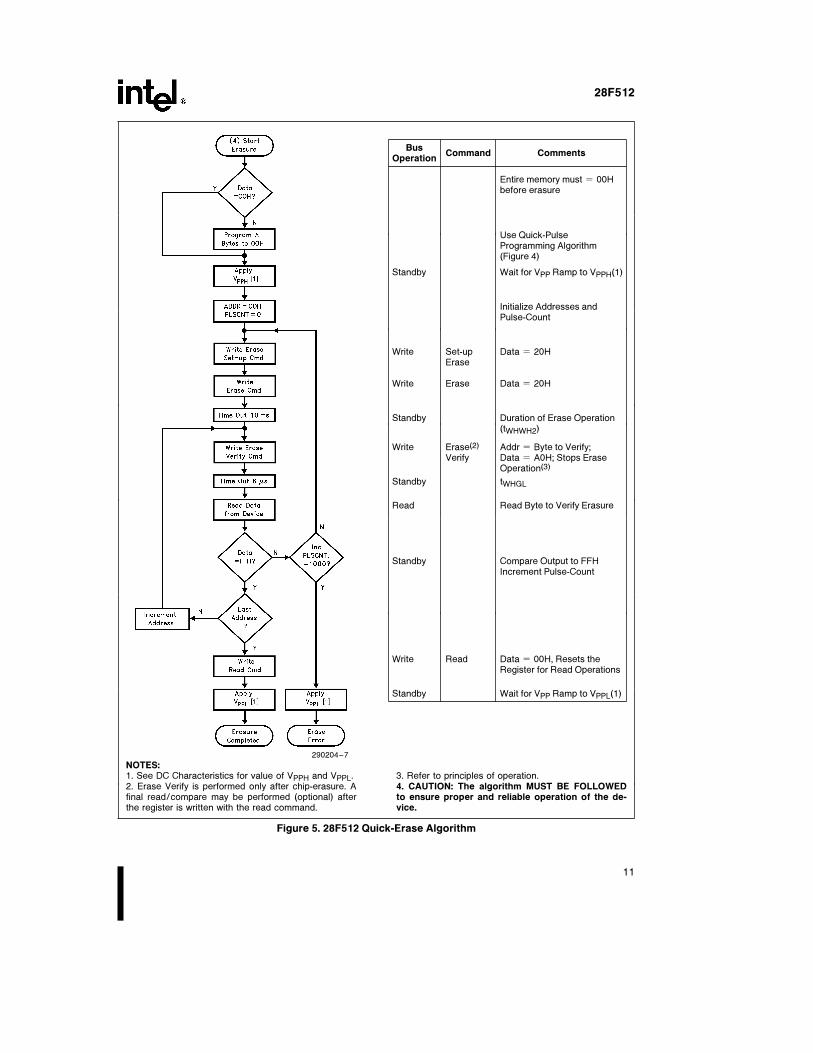
In the case where the data read is not FFH, anothererase operation is performed. (Refer to Set-upErase/Erase). Verification then resumes from theaddress of the last-verified byte. Once all bytes inthe array have been verified, the erase step is com-plete. The device can be programmed. At this point,the verify operation is terminated by writing a validcommand (e.g. Program Set-up) to the commandregister. Figure 5, the Quick-Erase algorithm, illus-trates how commands and bus operations are com-bined to perform electrical erasure of the 28F512.Refer to AC Erase Characteristics and Waveformsfor specific timing parameters.
Set-up Program/Program Commands
Set-up program is a command-only operation thatstages the device for byte programming. Writing 40Hinto the command register performs the set-upoperation.
Once the program set-up operation is performed,the next Write-Enable pulse causes a transition toan active programming operation. Addresses are in-ternally latched on the falling edge of the Write-En-able pulse. Data is internally latched on the risingedge of the Write-Enable pulse. The rising edge ofWrite-Enable also begins the programming opera-tion. The programming operation terminates with thenext rising edge of Write-Enable, used to write theprogram-verify command. Refer to AC ProgrammingCharacteristics and Waveforms for specific timingparameters.
8

28F512
Program-Verify Command
The 28F512 is programmed on a byte-by-byte basis.Byte programming may occur sequentially or at ran-dom. Following each programming operation, thebyte just programmed must be verified.
The program-verify operation is initiated by writingC0H into the command register. The register writeterminates the programming operation with the ris-ing edge of its Write-Enable pulse. The program-ver-ify operation stages the device for verification of thebyte last programmed. No new address informationis latched.
The 28F512 applies an internally-generated marginvoltage to the byte. A microprocessor read cycleoutputs the data. A successful comparison betweenthe programmed byte and true data means that thebyte is successfully programmed. Programming thenproceeds to the next desired byte location. Figure 4,the 28F512 Quick-Pulse Programming algorithm, il-lustrates how commands are combined with bus op-erations to perform byte programming. Refer to ACProgramming Characteristics and Waveforms forspecific timing parameters.
Reset Command
A reset command is provided as a means to safelyabort the erase- or program-command sequences.Following either set-up command (erase or program)with two consecutive writes of FFH will safely abortthe operation. Memory contents will not be altered.A valid command must then be written to place thedevice in the desired state.
EXTENDED ERASE/PROGRAM CYCLING
EEPROM cycling failures have always concernedusers. The high electrical field required by thin oxideEEPROMs for tunneling can literally tear apart theoxide at defect regions. To combat this, some sup-pliers have implemented redundancy schemes, re-ducing cycling failures to insignificant levels. Howev-er, redundancy requires that cell size be doubledÐan expensive solution.
Intel has designed extended cycling capability intoits ETOX II flash memory technology. Resulting im-provements in cycling reliability come without in-creasing memory cell size or complexity. First, anadvanced tunnel oxide increases the charge carry-ing ability ten-fold. Second, the oxide area per cellsubjected to the tunneling electric field is one-tenththat of common EEPROMs, minimizing the probabili-ty of oxide defects in the region. Finally, the peakelectric field during erasure is approximately 2 MV/cm lower than EEPROM. The lower electric field
greatly reduces oxide stress and the probability offailureÐincreasing time to wearout by a factor of100,000,000.
The 28F512 is capable of 100,000 program/erasecycles. The device is programmed and erased usingIntel’s Quick-Pulse Programming and Quick-Erasealgorithms. Intel’s algorithmic approach uses a se-ries of operations (pulses), along with byte verifica-tion, to completely and reliably erase and programthe device.
For further information, see Reliability Report RR-60(ETOX-II Reliability Data Summary).
QUICK-PULSE PROGRAMMING ALGORITHM
The Quick-Pulse Programming algorithm uses pro-gramming operations of 10 ms duration. Each opera-tion is followed by a byte verification to determinewhen the addressed byte has been successfully pro-grammed. The algorithm allows for up to 25 pro-gramming operations per byte, although most bytesverify on the first or second operation. The entiresequence of programming and byte verification isperformed with VPP at high voltage. Figure 4 illus-trates the Quick-Pulse Programming algorithm.
QUICK-ERASE ALGORITHM
Intel’s Quick-Erase algorithm yields fast and reliableelectrical erasure of memory contents. The algo-rithm employs a closed-loop flow, similar to theQuick-Pulse Programming algorithm, to simulta-neously remove charge from all bits in the array.
Erasure begins with a read of memory contents. The28F512 is erased when shipped from the factory.Reading FFH data from the device would immedi-ately be followed by device programming.
For devices being erased and reprogrammed, uni-form and reliable erasure is ensured by first pro-gramming all bits in the device to their charged state(Data e 00H). This is accomplished, using theQuick-Pulse Programming algorithm, in approxi-mately one second.
Erase execution then continues with an initial eraseoperation. Erase verification (data e FFH) begins ataddress 0000H and continues through the array tothe last address, or until data other than FFH is en-countered. With each erase operation, an increasingnumber of bytes verify to the erased state. Eraseefficiency may be improved by storing the address ofthe last byte verified in a register. Following the nexterase operation, verification starts at that stored ad-dress location. Erasure typically occurs in one sec-ond. Figure 5 illustrates the Quick-Erase algorithm.
9

28F512
290204–6
BusCommand Comments
Operation
Standby Wait for VPP Ramp to VPPH(1)
Initialize Pulse-Count
Write Set-up Data e 40HProgram
Write Program Valid Address/Data
Standby Duration of ProgramOperation (tWHWH1)
Write Program(2) Data e C0H; Stops ProgramVerify Operation(3)
Standby tWHGL
Read Read Byte to VerifyProgramming
Standby Compare Data Output to DataExpected
Write Read Data e 00H, Resets theRegister for Read Operations
Standby Wait for VPP Ramp to VPPL(1)
NOTES:1. See DC Characteristics for value of VPPH and VPPL.2. Program Verify is only performed after byte program-ming. A final read/compare may be performed (option-al) after the register is written with the Read command.
3. Refer to principles of operation.4. CAUTION: The algorithm MUST BE FOLLOWEDto ensure proper and reliable operation of the de-vice.
Figure 4. 28F512 Quick-Pulse Programming Algorithm
10
28F512
290204–7
BusCommand Comments
Operation
Entire memory must e 00Hbefore erasure
Use Quick-PulseProgramming Algorithm(Figure 4)
Standby Wait for VPP Ramp to VPPH(1)
Initialize Addresses andPulse-Count
Write Set-up Data e 20HErase
Write Erase Data e 20H
Standby Duration of Erase Operation(tWHWH2)
Write Erase(2) Addr e Byte to Verify;Verify Data e A0H; Stops Erase
Operation(3)
Standby tWHGL
Read Read Byte to Verify Erasure
Standby Compare Output to FFHIncrement Pulse-Count
Write Read Data e 00H, Resets theRegister for Read Operations
Standby Wait for VPP Ramp to VPPL(1)
NOTES:1. See DC Characteristics for value of VPPH and VPPL.2. Erase Verify is performed only after chip-erasure. Afinal read/compare may be performed (optional) afterthe register is written with the read command.
3. Refer to principles of operation.4. CAUTION: The algorithm MUST BE FOLLOWEDto ensure proper and reliable operation of the de-vice.
Figure 5. 28F512 Quick-Erase Algorithm
11

28F512
DESIGN CONSIDERATIONS
Two-Line Output Control
Flash-memories are often used in larger memory ar-rays. Intel provides two read-control inputs to ac-commodate multiple memory connections. Two-linecontrol provides for:
a. the lowest possible memory power dissipationand,
b. complete assurance that output bus contentionwill not occur.
To efficiently use these two control inputs, an ad-dress-decoder output should drive chip-enable,while the system’s read signal controls all flash-memories and other parallel memories. This assuresthat only enabled memory devices have active out-puts, while deselected devices maintain the lowpower standby condition.
Power Supply Decoupling
Flash-memory power-switching characteristics re-quire careful device decoupling. System designersare interested in three supply current (ICC) issuesÐstandby, active, and transient current peaks pro-duced by falling and rising edges of chip-enable. Thecapacitive and inductive loads on the device outputsdetermine the magnitudes of these peaks.
Two-line control and proper decoupling capacitorselection will suppress transient voltage peaks.Each device should have a 0.1 mF ceramic capacitorconnected between VCC and VSS, and between VPPand VSS.
Place the high-frequency, low-inherent-inductancecapacitors as close as possible to the devices. Also,for every eight devices, a 4.7 mF electrolytic capaci-tor should be placed at the array’s power supplyconnection, between VCC and VSS. The bulk capaci-tor will overcome voltage slumps caused by printed-circuit-board trace inductance, and will supplycharge to the smaller capacitors as needed.
VPP Trace on Printed Circuit Boards
Programming flash-memories, while they reside inthe target system, requires that the printed circuitboard designer pay attention to the VPP power sup-ply trace. The VPP pin supplies the memory cell cur-rent for programming. Use similar trace widths andlayout considerations given the VCC power bus. Ad-equate VPP supply traces and decoupling will de-crease VPP voltage spikes and overshoots.
Power Up/Down Protection
The 28F512 is designed to offer protection againstaccidental erasure or programming during powertransitions. Upon power-up, the 28F512 is indifferentas to which power supply, VPP or VCC, powers upfirst. Power supply sequencing is not required. Inter-nal circuitry in the 28F512 ensures that the com-mand register is reset to the read mode on powerup.
A system designer must guard against active writesfor VCC voltages above VLKO when VPP is active.Since both WEÝ and CEÝ must be low for a com-mand write, driving either to VIH will inhibit writes.The control register architecture provides an addedlevel of protection since alteration of memory con-tents only occurs after successful completion of thetwo-step command sequences.
28F512 Power Dissipation
When designing portable systems, designers mustconsider battery power consumption not only duringdevice operation, but also for data retention duringsystem idle time. Flash memory nonvolatility in-creases the usable battery life of your system be-cause the 28F512 does not consume any power toretain code or data when the system is off. Table 4illustrates the power dissipated when updating the28F512.
Table 4. 28F512 Typical Update
Power Dissipation(4)
Operation NotesPower Dissipation
(Watt-Seconds)
Array Program/ 1 0.085
Program Verify
Array Erase/ 2 0.092
Erase Verify
One Complete Cycle 3 0.262
NOTES:1. Formula to calculate typical Program/Program VerifyPower e [VPP c Ý Bytes x Typical Ý Prog Pulses(tWHWH1 c IPP2 Typical a tWHGL c IPP4 Typical)] a
[VCC c Ý Bytes c Typical Ý Prog Pulses (tWHWH1 c
ICC2 Typical a tWHGL c ICC4 Typical).2. Formula to calculate typical Erase/Erase Verify Powere [VPP(IPP3 Typical c tERASE Typical a IPP5 Typical c
tWHGL c Ý Bytes)] a [VCC(ICC3 Typical c tERASE Typi-cal a ICC5 Typical c tWHGL c Ý Bytes)].3. One Complete Cycle e Array Preprogram a ArrayErase a Program.4. ‘‘Typicals’’ are not guaranteed, but based on a limitednumber of samples from production lots.
12

28F512
ABSOLUTE MAXIMUM RATINGS*
Operating TemperatureDuring Read ÀÀÀÀÀÀÀÀÀÀÀÀÀÀÀÀÀÀ0§C to a70§C(1)
During Erase/Program ÀÀÀÀÀÀÀÀÀ0§C to a70§C(1)
Operating TemperatureDuring Read ÀÀÀÀÀÀÀÀÀÀÀÀÀÀÀb40§C to a85§C(2)
During Erase/Program ÀÀÀÀÀÀb40§C to a85§C(2)
Temperature Under BiasÀÀÀÀÀÀÀb10§C to a80§C(1)
Temperature Under BiasÀÀÀÀÀÀÀb50§C to a95§C(2)
Storage Temperature ÀÀÀÀÀÀÀÀÀÀb65§C to a125§CVoltage on Any Pin with
Respect to Ground ÀÀÀÀÀÀÀÀÀÀb2.0V to a7.0V(2)
Voltage on Pin A9 withRespect to Ground ÀÀÀÀÀÀÀb2.0V to a13.5V(2, 3)
VPP Supply Voltage withRespect to GroundDuring Erase/ProgramÀÀÀÀb2.0V to a14.0V(2, 3)
VCC Supply Voltage withRespect to Ground ÀÀÀÀÀÀÀÀÀÀb2.0V to a7.0V(2)
Output Short Circuit CurrentÀÀÀÀÀÀÀÀÀÀÀÀÀ100 mA(4)
NOTICE: This is a production data sheet. The specifi-cations are subject to change without notice.
*WARNING: Stressing the device beyond the ‘‘AbsoluteMaximum Ratings’’ may cause permanent damage.These are stress ratings only. Operation beyond the‘‘Operating Conditions’’ is not recommended and ex-tended exposure beyond the ‘‘Operating Conditions’’may affect device reliability.
NOTES:1. Operating temperature is for commercial product defined by this specification.2. Operating temperature is for extended temperature product defined by this specification.3. Minimum DC input voltage is b0.5V. During transitions, inputs may undershoot to b2.0V for periods less than 20 ns.Maximum DC voltage on output pins is VCC a 0.5V, which may overshoot to VCC a 2.0V for periods less than 20 ns.4. Maximum DC voltage on A9 or VPP may overshoot to a14.0V for periods less than 20 ns.5. Output shorted for no more than one second. No more than one output shorted at a time.
OPERATING CONDITIONS
Symbol ParameterLimits
Unit CommentsMin Max
TA Operating Temperature(1) 0 70 §C For Read-Only and
Read/Write Operations
for Commercial Products
TA Operating Temperature(2) b40 a85 §C For Read-Only and
Read/Write Operations
for Extended Temperature Products
VCC VCC Supply Voltage 4.50 5.50 V
DC CHARACTERISTICSÐTTL/NMOS COMPATIBLEÐCommercial Products
Symbol Parameter NotesLimits
Unit Test ConditionsMin Typ(4) Max
ILI Input Leakage Current 1 g1.0 mA VCC e VCC Max
VIN e VCC or VSS
ILO Output Leakage Current 1 g10.0 mA VCC e VCC Max
VOUT e VCC or VSS
ICCS VCC Standby Current 1 0.3 1.0 mA VCC e VCC Max
CEÝ e VIH
ICC1 VCC Active Read Current 1 10 30 mA VCC e VCC Max, CEÝ e VIL
f e 6 MHz, IOUT e 0 mA
ICC2 VCC Programming 1, 2 1.0 10 mA Programming in ProgressCurrent
ICC3 VCC Erase Current 1, 2 5.0 15 mA Erasure in Progress
ICC4 VCC Program Verify 1, 2 5.0 15 mA VPP e VPPHCurrent Program Verify in Progress
13

28F512
DC CHARACTERISTICSÐTTL/NMOS COMPATIBLEÐCommercial Products(Continued)
Symbol Parameter NotesLimits
Unit Test ConditionsMin Typ(4) Max
ICC5 VCC Erase Verify Current 1, 2 5.0 15 mA VPP e VPPH
Erase Verify in Progress
IPPS VPP Leakage Current 1 g10.0 mA VPP s VCC
IPP1 VPP Read Current, Standby 1 90 200 mA VPP l VCCCurrent, or ID Current
g10.0 VPP s VCC
IPP2 VPP Programming Current 1, 2 8.0 30 mA VPP e VPPH
Programming in Progress
IPP3 VPP Erase Current 1, 2 4.0 30 mA VPP e VPPH
Erasure in Progress
IPP4 VPP Program Verify Current 1, 2 2.0 5.0 mA VPP e VPPH
Program Verify in Progress
IPP5 VPP Erase Verify Current 1, 2 2.0 5.0 mA VPP e VPPH
Erase Verify in Progress
VIL Input Low Voltage b0.5 0.8 V
VIH Input High Voltage 2.0 VCC a 0.5 V
VOL Output Low Voltage 0.45 V IOL e 5.8 mA
VCC e VCC Min
VOH1 Output High Voltage 2.4 V IOH e b2.5 mA
VCC e VCC Min
VID A9 Intelligent Identifier Voltage 11.50 13.00 V
IID A9 Intelligent Identifier Current 1, 2 90 200 mA A9 e VID
VPPL VPP during Read-Only 0.00 6.5 V NOTE: Erase/Program areOperations Inhibited when VPP e VPPL
VPPH VPP during Read/Write 11.40 12.60 VOperations
VLKO VCC Erase/Write Lock Voltage 2.5 V
DC CHARACTERISTICSÐCMOS COMPATIBLEÐCommercial Products
Symbol Parameter NotesLimits
Unit Test ConditionsMin Typ(4) Max
ILI Input Leakage Current 1 g1.0 mA VCC e VCC Max
VIN e VCC or VSS
ILO Output Leakage Current 1 g10.0 mA VCC e VCC Max
VOUT e VCC or VSS
ICCS VCC Standby Current 1 50 100 mA VCC e VCC Max
CEÝ e VCC g0.2V
ICC1 VCC Active Read Current 1 10 30 mA VCC e VCC Max, CEÝ e VIL
f e 6 MHz, IOUT e 0 mA
14
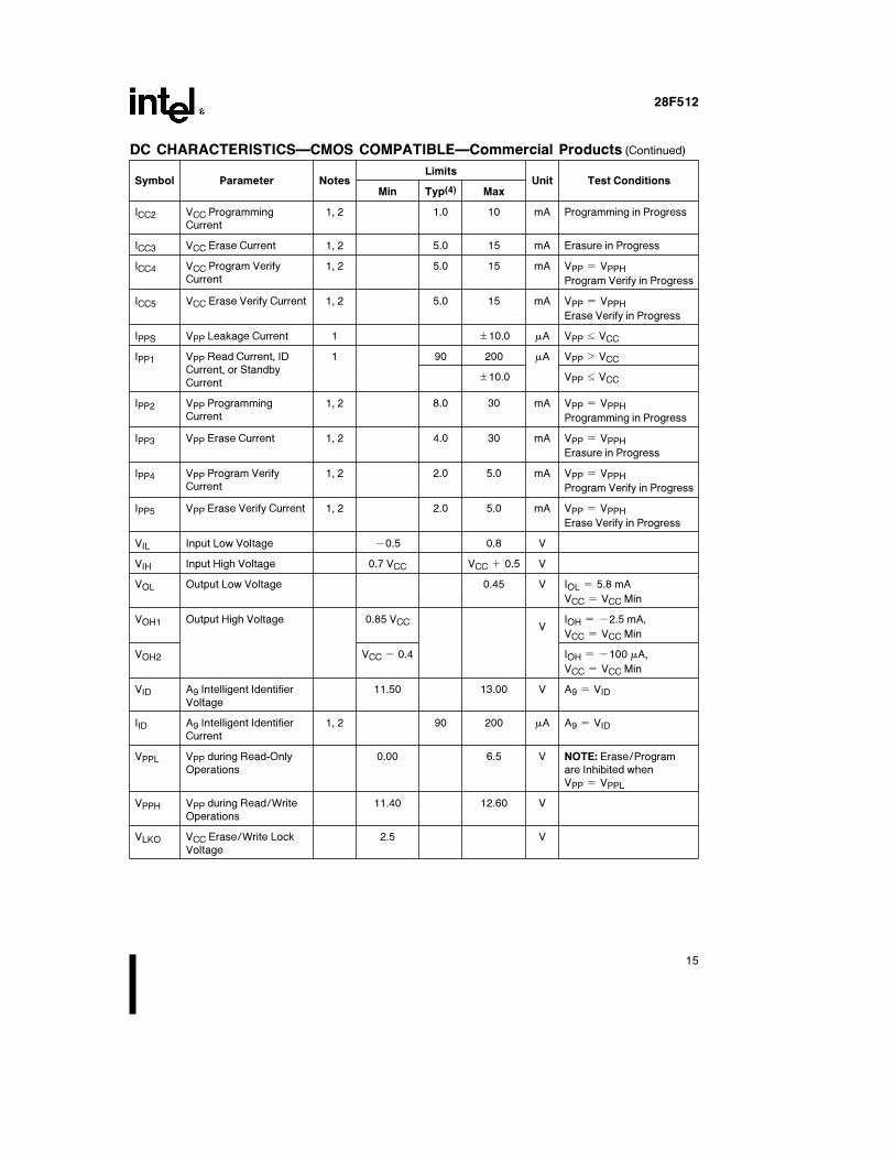
28F512
DC CHARACTERISTICSÐCMOS COMPATIBLEÐCommercial Products (Continued)
Symbol Parameter NotesLimits
Unit Test ConditionsMin Typ(4) Max
ICC2 VCC Programming 1, 2 1.0 10 mA Programming in ProgressCurrent
ICC3 VCC Erase Current 1, 2 5.0 15 mA Erasure in Progress
ICC4 VCC Program Verify 1, 2 5.0 15 mA VPP e VPPHCurrent Program Verify in Progress
ICC5 VCC Erase Verify Current 1, 2 5.0 15 mA VPP e VPPH
Erase Verify in Progress
IPPS VPP Leakage Current 1 g10.0 mA VPP s VCC
IPP1 VPP Read Current, ID 1 90 200 mA VPP l VCCCurrent, or Standby
g10.0 VPP s VCCCurrent
IPP2 VPP Programming 1, 2 8.0 30 mA VPP e VPPHCurrent Programming in Progress
IPP3 VPP Erase Current 1, 2 4.0 30 mA VPP e VPPH
Erasure in Progress
IPP4 VPP Program Verify 1, 2 2.0 5.0 mA VPP e VPPHCurrent Program Verify in Progress
IPP5 VPP Erase Verify Current 1, 2 2.0 5.0 mA VPP e VPPH
Erase Verify in Progress
VIL Input Low Voltage b0.5 0.8 V
VIH Input High Voltage 0.7 VCC VCC a 0.5 V
VOL Output Low Voltage 0.45 V IOL e 5.8 mA
VCC e VCC Min
VOH1 Output High Voltage 0.85 VCC VIOH e b2.5 mA,
VCC e VCC Min
VOH2 VCC b 0.4 IOH e b100 mA,
VCC e VCC Min
VID A9 Intelligent Identifier 11.50 13.00 V A9 e VIDVoltage
IID A9 Intelligent Identifier 1, 2 90 200 mA A9 e VIDCurrent
VPPL VPP during Read-Only 0.00 6.5 V NOTE: Erase/ProgramOperations are Inhibited when
VPP e VPPL
VPPH VPP during Read/Write 11.40 12.60 VOperations
VLKO VCC Erase/Write Lock 2.5 VVoltage
15

28F512
DC CHARACTERISTICSÐTTL/NMOS COMPATIBLEÐExtended TemperatureProducts
Symbol Parameter NotesLimits
Unit Test ConditionsMin Typ(4) Max
ILI Input Leakage Current 1 g1.0 mA VCC e VCC Max
VIN e VCC or VSS
ILO Output Leakage Current 1 g10.0 mA VCC e VCC Max
VOUT e VCC or VSS
ICCS VCC Standby Current 1 0.3 1.0 mA VCC e VCC Max
CEÝ e VIH
ICC1 VCC Active Read Current 1 10 30 mA VCC e VCC Max, CEÝ e VIL
f e 6 MHz, IOUT e 0 mA
ICC2 VCC Programming Current 1, 2 1.0 30 mA Programming in Progress
ICC3 VCC Erase Current 1, 2 5.0 30 mA Erasure in Progress
ICC4 VCC Program Verify Current 1, 2 5.0 30 mA VPP e VPPH
Program Verify in Progress
ICC5 VCC Erase Verify Current 1, 2 5.0 30 mA VPP e VPPH
Erase Verify in Progress
IPPS VPP Leakage Current 1 g10.0 mA VPP s VCC
IPP1 VPP Read Current, Standby 1 90 200 mA VPP l VCCCurrent, or ID Current
g10.0 VPP s VCC
IPP2 VPP Programming Current 1, 2 8.0 30 mA VPP e VPPH
Programming in Progress
IPP3 VPP Erase Current 1, 2 4.0 30 mA VPP e VPPH
Erasure in Progress
IPP4 VPP Program Verify Current 1, 2 2.0 5.0 mA VPP e VPPH
Program Verify in Progress
IPP5 VPP Erase Verify Current 1, 2 2.0 5.0 mA VPP e VPPH
Erase Verify in Progress
VIL Input Low Voltage b0.5 0.8 V
VIH Input High Voltage 2.0 VCC a 0.5 V
VOL Output Low Voltage 0.45 V IOL e 5.8 mA
VCC e VCC Min
VOH1 Output High Voltage 2.4 V IOH e b2.5 mA
VCC e VCC Min
VID A9 Intelligent Identifier Voltage 11.50 13.00 V
IID A9 Intelligent Identifier Current 1, 2 90 500 mA A9 e VID
VPPL VPP during Read-Only 0.00 6.5 V NOTE: Erase/Program areOperations Inhibited when VPP e VPPL
VPPH VPP during Read/Write 11.40 12.60 VOperations
VLKO VCC Erase/Write Lock Voltage 2.5 V
16

28F512
DC CHARACTERISTICSÐCMOS COMPATIBLEÐExtended TemperatureProducts
Symbol Parameter NotesLimits
Unit Test ConditionsMin Typ(4) Max
ILI Input Leakage Current 1 g1.0 mA VCC e VCC Max
VIN e VCC or VSS
ILO Output Leakage Current 1 g10.0 mA VCC e VCC Max
VOUT e VCC or VSS
ICCS VCC Standby Current 1 50 100 mA VCC e VCC Max
CEÝ e VCC g0.2V
ICC1 VCC Active Read Current 1 10 50 mA VCC e VCC Max, CEÝ e VIL
f e 6 MHz, IOUT e 0 mA
ICC2 VCC Programming Current 1, 2 1.0 10 mA Programming in Progress
ICC3 VCC Erase Current 1, 2 5.0 15 mA Erasure in Progress
ICC4 VCC Program Verify 1, 2 5.0 30 mA VPP e VPPHCurrent Program Verify in Progress
ICC5 VCC Erase Verify Current 1, 2 5.0 30 mA VPP e VPPH
Erase Verify in Progress
IPPS VPP Leakage Current 1 g10.0 mA VPP s VCC
IPP1 VPP Read Current, ID 1 90 200 mA VPP l VCCCurrent, or Standby
g10.0 VPP s VCCCurrent
IPP2 VPP Programming Current 1, 2 8.0 30 mA VPP e VPPH
Programming in Progress
IPP3 VPP Erase Current 1, 2 4.0 30 mA VPP e VPPH
Erasure in Progress
IPP4 VPP Program Verify 1, 2 2.0 5.0 mA VPP e VPPHCurrent Program Verify in Progress
IPP5 VPP Erase Verify Current 1, 2 2.0 5.0 mA VPP e VPPH
Erase Verify in Progress
VIL Input Low Voltage b0.5 0.8 V
VIH Input High Voltage 0.7 VCC VCC a 0.5 V
VOL Output Low Voltage 0.45 V IOL e 5.8 mA
VCC e VCC Min
17

28F512
DC CHARACTERISTICSÐCMOS COMPATIBLEÐExtended TemperatureProducts (Continued)
Symbol Parameter NotesLimits
Unit Test ConditionsMin Typ(4) Max
VOH1 Output High Voltage 0.85 VCC VIOH e b2.5 mA,
VCC e VCC Min
VOH2 VCC b 0.4 IOH e b100 mA,
VCC e VCC Min
VID A9 Intelligent Identifier Voltage 11.50 13.00 V A9 e VID
IID A9 Intelligent Identifier Current 1, 2 90 500 mA A9 e VID
VPPL VPP during Read-Only Operations 0.00 6.5 V NOTE: Erase/Programare InhibitedwhenVPP e VPPL
VPPH VPP during Read/Write Operations 11.40 12.60 V
VLKO VCC Erase/Write Lock Voltage 2.5 V
CAPACITANCE TA e 25§C, f e 1.0 MHz
Symbol Parameter NotesLimits
Unit ConditionsMin Max
CIN Address/Control Capacitance 3 8 pF VIN e 0V
COUT Output Capacitance 3 12 pF VOUT e 0V
NOTES:1. All currents are in RMS unless otherwise noted. Typical values at VCC e 5.0V, VPP e 12.0V, T e a25§C. Thesecurrents are valid for all product versions (packages and speeds).2. Not 100% tested: characterization data available.3. Sampled, not 100% tested.4. ‘‘Typicals’’ are not guaranteed, but based on a limited number of samples from production lots.
18

28F512
AC TESTING INPUT/OUTPUT WAVEFORM
290204–8
AC Testing: Inputs are driven at 2.4V for a logic ‘‘1’’ and 0.45V fora logic ‘‘0’’. Testing measurements are made at 2.0V for a logic‘‘1’’ and 0.8V for a logic ‘‘0’’. Rise/Fall time s 10 ns.
AC TESTING LOAD CIRCUIT
290204–9
CL e 100 pFCL includes Jig Capacitance
AC TEST CONDITIONS
Input Rise and Fall Times (10% to 90%)ÀÀÀÀÀÀ10 ns
Input Pulse Levels ÀÀÀÀÀÀÀÀÀÀÀÀÀÀÀÀ0.45V and 2.4V
Input Timing Reference Level ÀÀÀÀÀÀÀ0.8V and 2.0V
Output Timing Reference Level ÀÀÀÀÀÀ0.8V and 2.0V
AC CHARACTERISTICSÐRead-Only Operations
Versions(1)
Notes
N28F512-120
N28F512-150
P28F512-150 Unit
TN28F512-120
P28F512-120
TP28F512-120
Symbol Characteristic Min Max Min Max
tAVAV/tRC Read Cycle Time 120 150 ns
tELQV/tCE Chip Enable Access Time 120 150 ns
tAVQV/tACC Address Access Time 120 150 ns
tGLQV/tOE Output Enable Access Time 50 55 ns
tELQX/tLZ Chip Enable to Output in Low Z 2, 3 0 0 ns
tEHQZ Chip Disable to Output in High Z 2 55 55 ns
tGLQX/tOLZ Output Enable to Output in Low Z 2, 3 0 0 ns
tGHQZ/tDF Output Disable to Output in High Z 2 30 35 ns
tOH Output Hold from Address, CEÝ, or 2, 4 0 0 nsOEÝ Change
tWHGL Write Recovery Time before Read 6 6 ms
NOTES:1. Model number prefixes: N e PLCC, P e PDIP, T e Extended Temperature.2. Sampled, not 100% tested.3. Guaranteed by design.4. Whichever occurs first.
19

28F512
Figure 6. AC Waveforms for Read Operations
290204–10
20
28F512
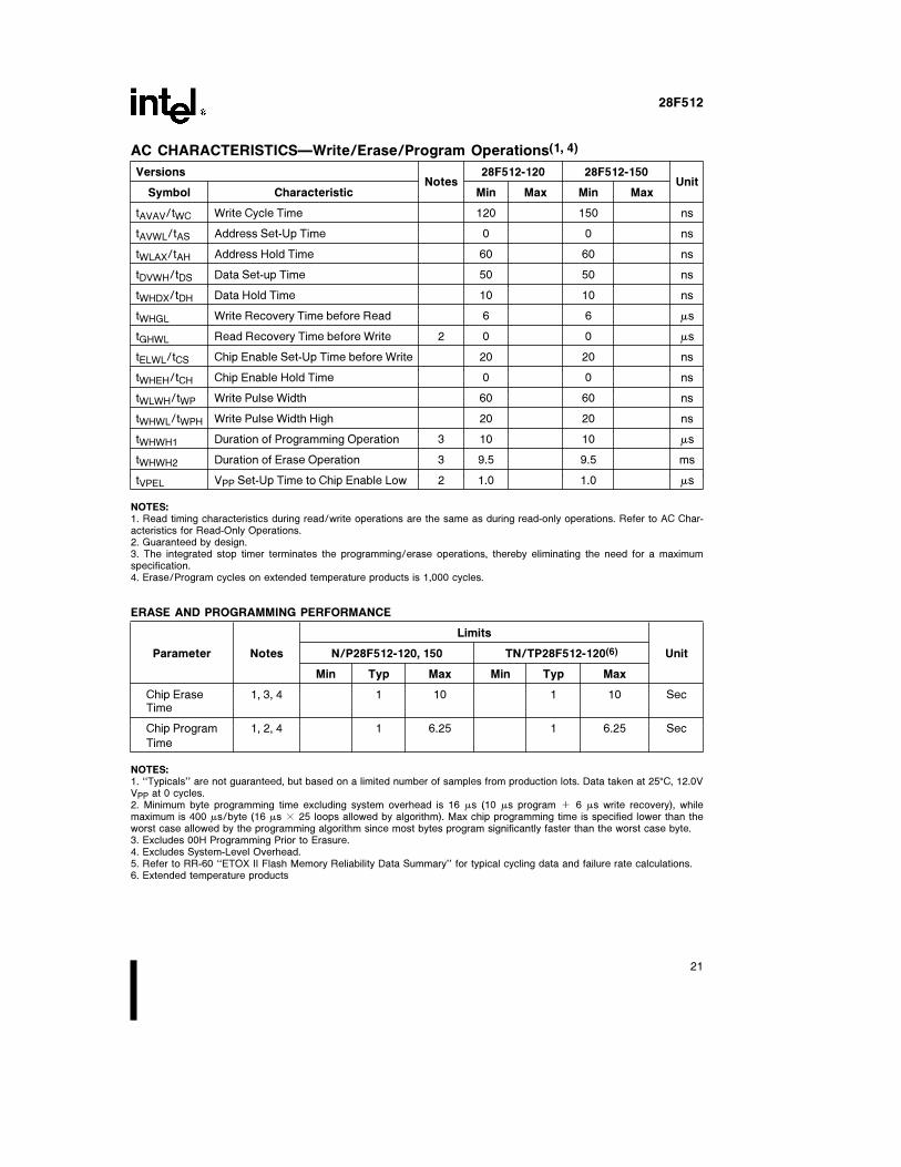
AC CHARACTERISTICSÐWrite/Erase/Program Operations(1, 4)
VersionsNotes
28F512-120 28F512-150Unit
Symbol Characteristic Min Max Min Max
tAVAV/tWC Write Cycle Time 120 150 ns
tAVWL/tAS Address Set-Up Time 0 0 ns
tWLAX/tAH Address Hold Time 60 60 ns
tDVWH/tDS Data Set-up Time 50 50 ns
tWHDX/tDH Data Hold Time 10 10 ns
tWHGL Write Recovery Time before Read 6 6 ms
tGHWL Read Recovery Time before Write 2 0 0 ms
tELWL/tCS Chip Enable Set-Up Time before Write 20 20 ns
tWHEH/tCH Chip Enable Hold Time 0 0 ns
tWLWH/tWP Write Pulse Width 60 60 ns
tWHWL/tWPH Write Pulse Width High 20 20 ns
tWHWH1 Duration of Programming Operation 3 10 10 ms
tWHWH2 Duration of Erase Operation 3 9.5 9.5 ms
tVPEL VPP Set-Up Time to Chip Enable Low 2 1.0 1.0 ms
NOTES:1. Read timing characteristics during read/write operations are the same as during read-only operations. Refer to AC Char-acteristics for Read-Only Operations.2. Guaranteed by design.3. The integrated stop timer terminates the programming/erase operations, thereby eliminating the need for a maximumspecification.4. Erase/Program cycles on extended temperature products is 1,000 cycles.
ERASE AND PROGRAMMING PERFORMANCE
Limits
Parameter Notes N/P28F512-120, 150 TN/TP28F512-120(6) Unit
Min Typ Max Min Typ Max
Chip Erase 1, 3, 4 1 10 1 10 SecTime
Chip Program 1, 2, 4 1 6.25 1 6.25 Sec
Time
NOTES:1. ‘‘Typicals’’ are not guaranteed, but based on a limited number of samples from production lots. Data taken at 25§C, 12.0VVPP at 0 cycles.2. Minimum byte programming time excluding system overhead is 16 ms (10 ms program a 6 ms write recovery), whilemaximum is 400 ms/byte (16 ms c 25 loops allowed by algorithm). Max chip programming time is specified lower than theworst case allowed by the programming algorithm since most bytes program significantly faster than the worst case byte.3. Excludes 00H Programming Prior to Erasure.4. Excludes System-Level Overhead.5. Refer to RR-60 ‘‘ETOX II Flash Memory Reliability Data Summary’’ for typical cycling data and failure rate calculations.6. Extended temperature products
21
28F512
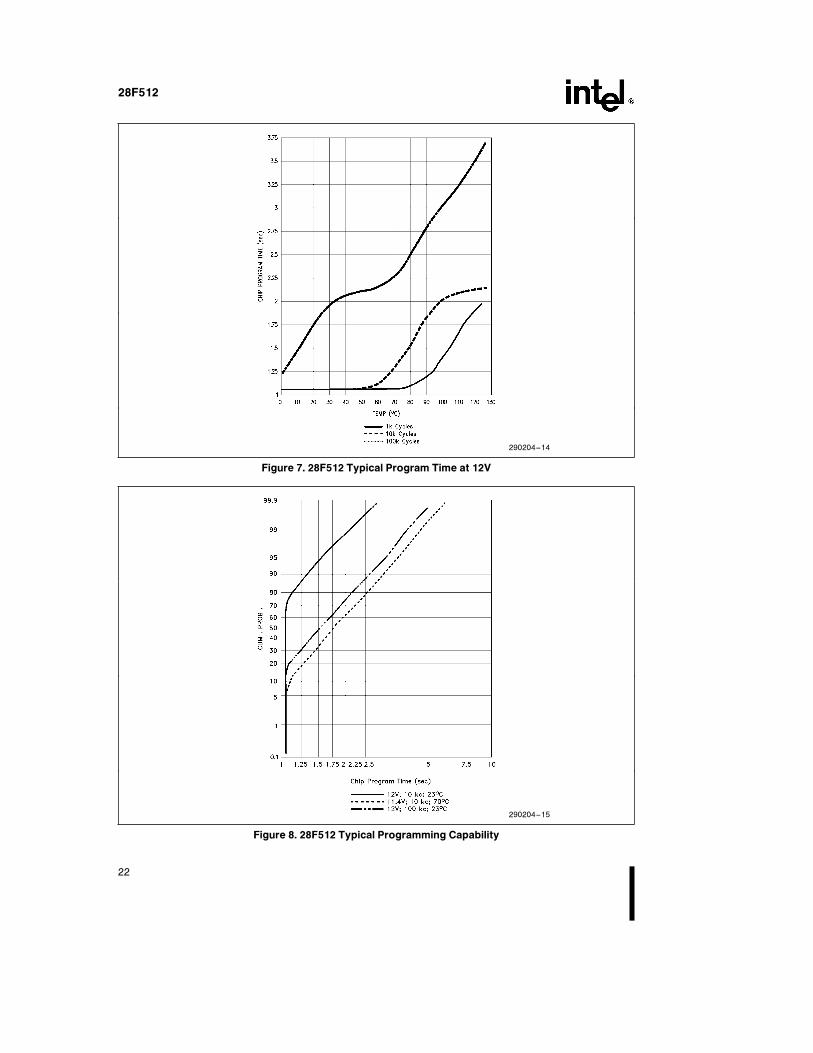
290204–14
Figure 7. 28F512 Typical Program Time at 12V
290204–15
Figure 8. 28F512 Typical Programming Capability
22

28F512
290204–16NOTE:Does not include Pre-Erase program.
Figure 9. 28F512 Typical Erase Time at 12V
290204–17NOTE:Does not include Pre-Erase program.
Figure 10. 28F512 Typical Erase Capability
23

28F512
Figure 11. AC Waveforms for Programming Operations
290204–19
24

28F512
ALTERNATIVE CEÝ-CONTROLLED WRITES
VersionsNotes
28F512-120 28F512-150Unit
Symbol Characteristic Min Max Min Max
tAVAV Write Cycle 120 150 nsTime
tAVEL Address Set- 0 0 nsUp Time
tELAX Address Hold 80 80 nsTime
tDVEH Data Set-Up 50 50 nsTime
tEHDX Data Hold 10 10 nsTime
tEHGL Write 6 6 msRecovery Timebefore Read
tGHEL Read 2 0 0 msRecovery Timebefore Write
tWLEL Write Enable 0 0 nsSet-Up Timebefore ChipEnable
tEHWH Write Enable 0 0 nsHold Time
tELEH Write Pulse 1 70 70 nsWidth
tEHEL Write Pulse 20 20 nsWidth High
tVPEL VPP Set-Up 2 1.0 1.0 msTime to ChipEnable Low
NOTE:1. Chip-Enable Controlled Writes: Write operations are driven by the valid combination of Chip-Enable and Write-Enable. Insystems where Chip-Enable defines the write pulse width (within a longer Write-Enable timing waveform) all set-up, hold andinactive Write-Enable times should be measured relative to the Chip-Enable waveform.2. Guaranteed by design.
25

28F512
Figure 12. AC Waveforms for Erase Operations
290204–20
26

28F512
Figure 13. Alternate AC Waveforms for Programming Operations
290204–21
27
28F512
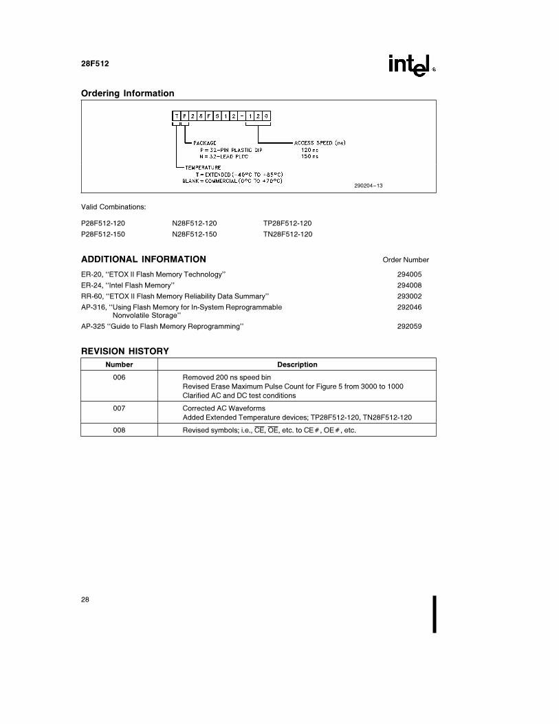
Ordering Information
290204–13
Valid Combinations:
P28F512-120
P28F512-150
N28F512-120
N28F512-150
TP28F512-120
TN28F512-120
ADDITIONAL INFORMATION Order Number
ER-20, ‘‘ETOX II Flash Memory Technology’’ 294005
ER-24, ‘‘Intel Flash Memory’’ 294008
RR-60, ‘‘ETOX II Flash Memory Reliability Data Summary’’ 293002
AP-316, ‘‘Using Flash Memory for In-System Reprogrammable 292046Nonvolatile Storage’’
AP-325 ‘‘Guide to Flash Memory Reprogramming’’ 292059
REVISION HISTORY
Number Description
006 Removed 200 ns speed bin
Revised Erase Maximum Pulse Count for Figure 5 from 3000 to 1000
Clarified AC and DC test conditions
007 Corrected AC Waveforms
Added Extended Temperature devices; TP28F512-120, TN28F512-120
008 Revised symbols; i.e., CE, OE, etc. to CEÝ, OEÝ, etc.
28