Embed Size (px)
Citation preview

GS82583ED18/36GK-675/625/550/500
288Mb SigmaQuad-IIIe™Burst of 4 SRAM
Up to 675 MHz1.3V VDD
1.2V, 1.3V, or 1.5V VDDQ
260-Pin BGACommercial TempIndustrial Temp
Features• 8Mb x 36 and 16Mb x 18 organizations available• 675 MHz maximum operating frequency• 675 MT/s peak transaction rate (in millions per second)• 97 Gb/s peak data bandwidth (in x36 devices)• Separate I/O DDR Data Buses• Non-multiplexed SDR Address Bus• One operation - Read or Write - per clock cycle• Burst of 4 Read and Write operations• 3 cycle Read Latency• 1.3V nominal core voltage• 1.2V, 1.3V, or 1.5V HSTL I/O interface• Configurable ODT (on-die termination)• ZQ pin for programmable driver impedance• ZT pin for programmable ODT impedance• IEEE 1149.1 JTAG-compliant Boundary Scan• 260-pin, 14 mm x 22 mm, 1 mm ball pitch, 6/6 RoHS-
compliant BGA package
SigmaQuad-IIIe™ Family OverviewSigmaQuad-IIIe SRAMs are the Separate I/O half of the SigmaQuad-IIIe/SigmaDDR-IIIe family of high performance SRAMs. Although very similar to GSI's second generation of networking SRAMs (the SigmaQuad-II/SigmaDDR-II family), these third generation devices offer several new features that help enable significantly higher performance.
Clocking and Addressing SchemesThe GS82583ED18/36GK SigmaQuad-IIIe SRAMs are synchronous devices. They employ three pairs of positive and negative input clocks; one pair of master clocks, CK and CK, and two pairs of write data clocks, KD[1:0] and KD[1:0]. All six input clocks are single-ended; that is, each is received by a dedicated input buffer.
CK and CK are used to latch address and control inputs, and to control all output timing. KD[1:0] and KD[1:0] are used solely to latch data inputs.
Each internal read and write operation in a SigmaQuad-IIIe B4 SRAM is four times wider than the device I/O bus. An input data bus de-multiplexer is used to accumulate incoming data before it is simultaneously written to the memory array. An output data multiplexer is used to capture the data produced from a single memory array read and then route it to the appropriate output drivers as needed. Therefore, the address field of a SigmaQuad-IIIe B4 SRAM is always two address pins less than the advertised index depth (e.g. the 16M x 18 has 4M addressable index).
Rev: 1.07 12/2017 1/26 © 2014, GSI TechnologySpecifications cited are subject to change without notice. For latest documentation see http://www.gsitechnology.com.
Parameter Synopsis
Speed Grade Max Operating Frequency Read Latency VDD
-675 675 MHz 3 cycles 1.25V to 1.35V
-625 625 MHz 3 cycles 1.25V to 1.35V
-550 550 MHz 3 cycles 1.25V to 1.35V
-500 500 MHz 3 cycles 1.25V to 1.35V

GS82583ED18/36GK-675/625/550/500
16M x 18 Pinout (Top View)
1 2 3 4 5 6 7 8 9 10 11 12 13
A VDD VDDQ VDD VDDQNC
(RSVD)MCH(CFG)
MCL ZQ PZT1 VDDQ VDD VDDQ VDD
B VSS NUO VSS NUI MVQ MCH(B4M)
NC(RSVD)
MCH(SIOM) PZT0 D0 VSS Q0 VSS
C Q17 VDDQ D17 VDDQ VSS SA VDD SA VSS VDDQ NUI VDDQ NUO
D VSS NUO VSS NUI SA VDDQ SA VDDQ SA D1 VSS Q1 VSS
E Q16 VDDQ D16 VDD VSS SA VSS SA VSS VDD NUI VDDQ NUO
F VSS NUO VSS NUI SA VDD VDDQ VDD SA D2 VSS Q2 VSS
G Q15 NUO D15 NUI VSS SA MZT1 SA VSS D3 NUI Q3 NUO
H Q14 VDDQ D14 VDDQ SA VDDQ W VDDQ SA VDDQ NUI VDDQ NUO
J VSS NUO VSS NUI VSS SA VSS SA VSS D4 VSS Q4 VSS
K CQ1 VDDQ VREF VDD KD1 VDD CK VDD KD0 VDD VREF VDDQ CQ0
L CQ1 VSS QVLD1 Vss KD1 VDDQ CK VDDQ KD0 VSS QVLD0 VSS CQ0
M VSS Q13 VSS D13 VSS SA VSS SA VSS NUI VSS NUO VSS
N NUO VDDQ NUI VDDQ DLL VDDQ R VDDQ MCH VDDQ D5 VDDQ Q5
P NUO Q12 NUI D12 VSS SA MZT0 SA VSS NUI D6 NUO Q6
R VSS Q11 VSS D11 MCH VDD VDDQ VDD RST NUI VSS NUO VSS
T NUO VDDQ NUI VDD VSS SA VSS SA VSS VDD D7 VDDQ Q7
U VSS Q10 VSS D10 NC(576 Mb)
VDDQNC
(RSVD)VDDQ
NC(1152 Mb)
NUI VSS NUO VSS
V NUO VDDQ NUI VDDQ VSSSA
(x18)VDD
NUI(B2)
VSS VDDQ D8 VDDQ Q8
W VSS Q9 VSS D9 TCK MCL NC(RSVD) MCL TMS NUI VSS NUO VSS
Y VDD VDDQ VDD VDDQ TDO ZT NC(RSVD) MCL TDI VDDQ VDD VDDQ VDD
Notes:1. Pins 6W, 7A, 8W, and 8Y must be tied Low in this device.2. Pins 5R and 9N must be tied High in this device.3. Pin 6A is defined as mode pin CFG in the pinout standard. It must be tied High in this device to select x18 configuration.4. Pin 8B is defined as mode pin SIOM in the pinout standard. It must be tied High in this device to select Separate I/O configuration.5. Pin 6B is defined as mode pin B4M in the pinout standard. It must be tied High in this device to select Burst-of-4 configuration.6. Pin 6V is defined as address pin SA for x18 devices. It is used in this device.7. Pin 8V is defined as address pin SA for B2 devices. It is unused in this device, and must be left unconnected or driven Low.8. Pin 5U is reserved as address pin SA for 576 Mb devices. It is a true no connect in this device.9. Pin 9U is reserved as address pin SA for 1152 Mb devices. It is a true no connect in this device.
Specifications cited are subject to change without notice. For latest documentation see http://www.gsitechnology.com.
Rev: 1.07 12/2017 2/26 © 2014, GSI Technology

GS82583ED18/36GK-675/625/550/500
8M x 36 Pinout (Top View)
1 2 3 4 5 6 7 8 9 10 11 12 13
A VDD VDDQ VDD VDDQNC
(RSVD)MCL
(CFG)MCL ZQ PZT1 VDDQ VDD VDDQ VDD
B VSS Q35 VSS D35 MVQ MCH(B4M)
NC(RSVD)
MCH(SIOM) PZT0 D0 VSS Q0 VSS
C Q26 VDDQ D26 VDDQ VSS SA VDD SA VSS VDDQ D9 VDDQ Q9
D VSS Q34 VSS D34 SA VDDQ SA VDDQ SA D1 VSS Q1 VSS
E Q25 VDDQ D25 VDD VSS SA VSS SA VSS VDD D10 VDDQ Q10
F VSS Q33 VSS D33 SA VDD VDDQ VDD SA D2 VSS Q2 VSS
G Q24 Q32 D24 D32 VSS SA MZT1 SA VSS D3 D11 Q3 Q11
H Q23 VDDQ D23 VDDQ SA VDDQ W VDDQ SA VDDQ D12 VDDQ Q12
J VSS Q31 VSS D31 VSS SA VSS SA VSS D4 VSS Q4 VSS
K CQ1 VDDQ VREF VDD KD1 VDD CK VDD KD0 VDD VREF VDDQ CQ0
L CQ1 VSS QVLD1 VSS KD1 VDDQ CK VDDQ KD0 VSS QVLD0 VSS CQ0
M VSS Q22 VSS D22 VSS SA VSS SA VSS D13 VSS Q13 VSS
N Q30 VDDQ D30 VDDQ DLL VDDQ R VDDQ MCH VDDQ D5 VDDQ Q5
P Q29 Q21 D29 D21 VSS SA MZT0 SA VSS D14 D6 Q14 Q6
R VSS Q20 VSS D20 MCH VDD VDDQ VDD RST D15 VSS Q15 VSS
T Q28 VDDQ D28 VDD VSS SA VSS SA VSS VDD D7 VDDQ Q7
U VSS Q19 VSS D19 NC(576 Mb) VDDQ
NC(RSVD) VDDQ
NC(1152 Mb) D16 VSS Q16 VSS
V Q27 VDDQ D27 VDDQ VSSNUI
(x18)VDD
NUI(B2)
VSS VDDQ D8 VDDQ Q8
W VSS Q18 VSS D18 TCK MCL NC(RSVD) MCL TMS D17 VSS Q17 VSS
Y VDD VDDQ VDD VDDQ TDO ZT NC(RSVD) MCL TDI VDDQ VDD VDDQ VDD
Notes:1. Pins 6W, 7A, 8W, and 8Y must be tied Low in this device.2. Pins 5R and 9N must be tied High in this device.3. Pin 6A is defined as mode pin CFG in the pinout standard. It must be tied Low in this device to select x36 configuration.4. Pin 8B is defined as mode pin SIOM in the pinout standard. It must be tied High in this device to select Separate I/O configuration.5. Pin 6B is defined as mode pin B4M in the pinout standard. It must be tied High in this device to select Burst-of-4 configuration.6. Pin 6V is defined as address pin SA for x18 devices. It is unused in this device, and must be left unconnected or driven Low.7. Pin 8V is defined as address pin SA for B2 devices. It is unused in this device, and must be left unconnected or driven Low.8. Pin 5U is reserved as address pin SA for 576 Mb devices. It is a true no connect in this device.9. Pin 9U is reserved as address pin SA for 1152 Mb devices. It is a true no connect in this device.
Specifications cited are subject to change without notice. For latest documentation see http://www.gsitechnology.com.
Rev: 1.07 12/2017 3/26 © 2014, GSI Technology

GS82583ED18/36GK-675/625/550/500
Pin Description
Symbol Description Type
SA Address — Read or Write Address is registered on CK. Input
D[35:0]Write Data — Registered on KD and KD during Write operations.
D[17:0] - x18 and x36.D[35:18] - x36 only.
Input
Q[35:0]Read Data — Aligned with CQ and CQ during Read operations.
Q[17:0] - x18 and x36.Q[35:18] - x36 only.
Output
QVLD[1:0] Read Data Valid — Driven high one half cycle before valid Read Data. Output
CK, CKPrimary Input Clocks — Dual single-ended. Used for latching address and control inputs, for internal timing control, and for output timing control.
Input
KD[1:0],KD[1:0]
Write Data Input Clocks — Dual single-ended. Used for latching write data inputs.KD0, KD0: latch Write Data (D[17:0] in x36, D[8:0] in x18).KD1, KD1: latch Write Data (D[35:18] in x36, D[17:9] in x18).
Input
CQ[1:0], CQ[1:0]
Read Data Output Clocks — Free-running output (echo) clocks, tightly aligned with read data outputs. Facilitate source-synchronous operation.
Output
R Read Enable — Registered on CK. R = 0 initiates a Read operation. Input
W Write Enable — Registered on CK. W = 0 initiates a Write operation. Input
DLLDLL Enable — Weakly pulled High internally.
DLL = 0: disables internal DLL.DLL = 1: enables internal DLL.
Input
RSTReset — Holds the device inactive and resets the device to its initial power-on state when asserted High. Weakly pulled Low internally.
Input
ZQDriver Impedance Control Resistor Input — Must be connected to VSS through an external resistor RQ to program driver impedance.
Input
ZTODT Impedance Control Resistor Input — Must be connected to VSS through an external resistor RT to program ODT impedance.
Input
MZT[1:0]
ODT Mode Select — Set the ODT state globally for all input groups. Must be tied High or Low.MZT[1:0] = 00: disables ODT on all input groups, regardless of PZT[1:0].MZT[1:0] = 01: enables strong ODT on select input groups, as specified by PZT[1:0].MZT[1:0] = 10: enables weak ODT on select input groups, as specified by PZT[1:0].MZT[1:0] = 11: reserved.
Input
PZT[1:0]
ODT Configuration Select — Set the ODT state for various combinations of input groups when MZT[1:0] = 01 or 10. Must be tied High or Low.
PZT[1:0] = 00: enables ODT on write data only.PZT[1:0] = 01: enables ODT on write data and input clocks.PZT[1:0] = 10: enables ODT on write data, address, and control.PZT[1:0] = 11: enables ODT on write data, input clocks, address, and control.
Input
Specifications cited are subject to change without notice. For latest documentation see http://www.gsitechnology.com.
Rev: 1.07 12/2017 4/26 © 2014, GSI Technology

GS82583ED18/36GK-675/625/550/500
MVQ
I/O Voltage Select — Indicates what voltage is supplied to the VDDQ pins. Must be tied High or Low.MVQ = 0: Configure for 1.2V or 1.3V nominal VDDQ.MVQ = 1: Configure for 1.5V nominal VDDQ.
Input
VDD Core Power Supply —
VDDQ I/O Power Supply —
VREF Input Reference Voltage — Input buffer reference voltage. —
VSS Ground —
TCK JTAG Clock — Weakly pulled Low internally. Input
TMS JTAG Mode Select — Weakly pulled High internally. Input
TDI JTAG Data Input — Weakly pulled High internally. Input
TDO JTAG Data Output Output
MCH Must Connect High — May be tied to VDDQ directly or via a 1k resistor. Input
MCL Must Connect Low — May be tied to VSS directly or via a 1k resistor. Input
NCNo Connect — There is no internal chip connection to these pins. They may be left unconnected, or tied/driven High or Low.
—
NUI
Not Used Input — There is an internal chip connection to these input pins, but they are unused by the device. They are pulled Low internally. They may be left unconnected or tied/driven Low. They should not be tied/driven High.
Input
NUONot Used Output — There is an internal chip connection to these output pins, but they are unused by the device. The drivers are tri-stated internally. They should be left unconnected.
Output
Symbol Description Type
Specifications cited are subject to change without notice. For latest documentation see http://www.gsitechnology.com.
Rev: 1.07 12/2017 5/26 © 2014, GSI Technology
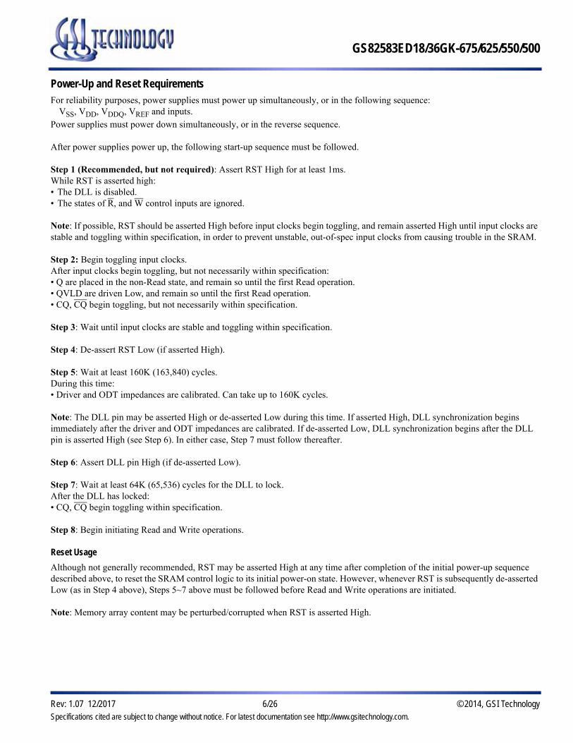
GS82583ED18/36GK-675/625/550/500
Power-Up and Reset RequirementsFor reliability purposes, power supplies must power up simultaneously, or in the following sequence:
VSS, VDD, VDDQ, VREF and inputs.Power supplies must power down simultaneously, or in the reverse sequence.
After power supplies power up, the following start-up sequence must be followed.
Step 1 (Recommended, but not required): Assert RST High for at least 1ms.While RST is asserted high:• The DLL is disabled.• The states of R, and W control inputs are ignored.
Note: If possible, RST should be asserted High before input clocks begin toggling, and remain asserted High until input clocks are stable and toggling within specification, in order to prevent unstable, out-of-spec input clocks from causing trouble in the SRAM.
Step 2: Begin toggling input clocks.After input clocks begin toggling, but not necessarily within specification:• Q are placed in the non-Read state, and remain so until the first Read operation.• QVLD are driven Low, and remain so until the first Read operation.• CQ, CQ begin toggling, but not necessarily within specification.
Step 3: Wait until input clocks are stable and toggling within specification.
Step 4: De-assert RST Low (if asserted High).
Step 5: Wait at least 160K (163,840) cycles.During this time:• Driver and ODT impedances are calibrated. Can take up to 160K cycles.
Note: The DLL pin may be asserted High or de-asserted Low during this time. If asserted High, DLL synchronization begins immediately after the driver and ODT impedances are calibrated. If de-asserted Low, DLL synchronization begins after the DLL pin is asserted High (see Step 6). In either case, Step 7 must follow thereafter.
Step 6: Assert DLL pin High (if de-asserted Low).
Step 7: Wait at least 64K (65,536) cycles for the DLL to lock.After the DLL has locked:• CQ, CQ begin toggling within specification.
Step 8: Begin initiating Read and Write operations.
Reset Usage
Although not generally recommended, RST may be asserted High at any time after completion of the initial power-up sequence described above, to reset the SRAM control logic to its initial power-on state. However, whenever RST is subsequently de-asserted Low (as in Step 4 above), Steps 5~7 above must be followed before Read and Write operations are initiated.
Note: Memory array content may be perturbed/corrupted when RST is asserted High.
Specifications cited are subject to change without notice. For latest documentation see http://www.gsitechnology.com.
Rev: 1.07 12/2017 6/26 © 2014, GSI Technology

GS82583ED18/36GK-675/625/550/500
DLL OperationA DLL is implemented in these devices to control all output timing. It uses the CK input clock as a source, and is enabled when all of the following conditions are met:
1. RST is de-asserted Low, and2. The DLL pin is asserted High, and3. CK cycle time tKHKH (max), as specified in the AC Timing Specifications section.
Once enabled, the DLL requires 64K stable clock cycles in order to lock/synchronize properly.
When the DLL is enabled, it aligns output clocks and read data to input clocks, and it generates all mid-cycle output timing. See the Output Timing section for more information.
The DLL can tolerate changes in input clock frequency due to clock jitter (i.e. such jitter will not cause the DLL to lose lock/synchronization), provided the cycle-to-cycle jitter does not exceed 200ps (see “tKJITcc” in the AC Timing Specifications section
for more information). However, the DLL must be resynchronized (i.e. disabled and then re-enabled) whenever the nominal input clock frequency is changed.
The DLL is disabled when any of the following conditions are met:
1. RST is asserted High, or2. The DLL pin is de-asserted Low, or3. CK is stopped for at least 30ns, or CK cycle time 30ns.
Clock Truth Table
Previous Operation
SA R W Current Operation D Q
(tn–1)CK(tn)
CK(tn)
CK(tn) (tn)
KD(tn+1)
KD(tn+1½)
KD(tn+2)
KD(tn+2½)
CQ(tn+3)
CQ(tn+3½)
CQ(tn+4)
CQ(tn+4½)
NOP X 1 1 NOP X X — — 0 / High-Z —
Write X 1 X NOP D3 D4 — — 0 / High-Z —
Read X X 1 NOP X X — — Q3 Q4 —
NOP V 1 0 Write D1 D2 D3 D4 0 / High-Z —
Read V X 0 Write D1 D2 D3 D4 Q3 Q4 —
NOP V 0 X Read X X — — Q1 Q2 Q3 Q4
Write V 0 X Read D3 D4 — — Q1 Q2 Q3 Q4
Notes:1. 1 = High; 0 = Low; V = Valid; X = don’t care.2. D1, D2, D3, and D4 indicate the first, second, third, and fourth pieces of Write Data transferred during Write operations.3. Q1, Q2, Q3, and Q4 indicate the first, second, third, and fourth pieces of Read Data transferred during Read operations.4. When D ODT is enabled, Q pins are driven Low for one cycle in response to NOP and Write commands, 3 cycles after the command is
sampled, except when preceded by a Read command. When D ODT is disabled, Q pins are tri-stated for one cycle in response to NOP and Write commands, 3 cycles after the command is sampled, except when preceded by a Read command.
Specifications cited are subject to change without notice. For latest documentation see http://www.gsitechnology.com.
Rev: 1.07 12/2017 7/26 © 2014, GSI Technology

GS82583ED18/36GK-675/625/550/500
Input TimingThese devices utilize three pairs of positive and negative input clocks, CK & CK and KD[1:0] & KD[1:0], to latch the various synchronous inputs. Specifically:
CK latches all address (SA) inputs.
CK latches all control (R, W) inputs.
KD[1:0] and KD[1:0] latch particular write data (D) inputs, as follows:
• KD0 and KD0 latch D[17:0] in x36, and D[8:0] in x18.• KD1 and KD1 latch D[35:18] in x36, and D[17:9] in x18.
Output TimingThese devices provide two pairs of positive and negative output clocks (aka “echo clocks”), CQ[1:0] & CQ[1:0], whose timing is tightly aligned with read data in order to enable reliable source-synchronous data transmission.
These devices utilize a DLL to control output timing. When the DLL is enabled, it generates 0 and 180 phase clocks from CK that control read data output clock (CQ, CQ), read data (Q), and read data valid (QVLD) output timing, as follows:
• CK+0 generates CQ[1:0], CQ[1:0], Q1 active, and Q2 inactive.• .CK+180 generates CQ[1:0], CQ[1:0], Q1 inactive, Q2 active, and QVLD active/inactive.
Note: Q1 and Q2 indicate the first and second pieces of read data transferred in any given clock cycle during Read operations.
When the DLL is enabled, CQ is aligned to CK. See the AC Timing Specifications for more information.
CQ[1:0] and CQ[1:0] align with particular Q and QVLD outputs, as follows:
• CQ0 and CQ0 align with Q[17:0], QVLD0 in x36 devices, and Q[8:0], QVLD0 in x18 devices. • CQ1 and CQ1 align with Q[35:18], QVLD1 in x36 devices, and Q[17:9], QVLD0 in x18 devices.
Specifications cited are subject to change without notice. For latest documentation see http://www.gsitechnology.com.
Rev: 1.07 12/2017 8/26 © 2014, GSI Technology

GS82583ED18/36GK-675/625/550/500
Driver Impedance ControlProgrammable Driver Impedance is implemented on the following output signals:
• CQ, CQ, Q, QVLD.
Driver impedance is programmed by connecting an external resistor RQ between the ZQ pin and VSS.
Driver impedance is set to the programmed value within 160K cycles after input clocks are operating within specification and RST is de-asserted Low. It is updated periodically thereafter to compensate for temperature and voltage fluctuations in the system.
Output Signal Pull-Down Impedance (ROUTL) Pull-Up Impedance (ROUTH)
CQ, CQ, Q, QVLD RQ*0.2 15% RQ*0.2 15%
Notes:1. ROUTL and ROUTH apply when 175 RQ 225.2. The mismatch between ROUTL and ROUTH is less than 10%, guaranteed by design.
ODT Impedance ControlProgrammable ODT Impedance is implemented on the following input signals:
• CK, CK, KD, KD, SA, R, W, D.
ODT impedance is programmed by connecting an external resistor RT between the ZT pin and VSS.
ODT impedance is set to the programmed value within 160K cycles after input clocks are operating within specification and RST is de-asserted Low. It is updated periodically thereafter to compensate for temperature and voltage fluctuations in the system
Input Signal PZT[1:0] MZT[1:0] Pull-Down Impedance (RINL) Pull-Up Impedance (RINH)
CK, CK, KD, KD
X0 XX disabled disabled
X101 RT 15% RT 15%
10 RT*2 20% RT*2 20%
SA, R, W
0X XX disabled disabled
1X01 RT 15% RT 15%
10 RT*2 20% RT*2 20%
D XX01 RT 15% RT 15%
10 RT*2 20% RT*2 20%
Notes: 1. When MZT[1:0] = 00, ODT is disabled on all inputs. MZT[1:0] = 11 is reserved for future use.2. RINL and RINH apply when 105 RT 1353. The mismatch between RINL and RINH is less than 10%, guaranteed by design.
4. All ODT is disabled during JTAG EXTEST and SAMPLE-Z instructions.
Note: When ODT impedance is enabled on a particular input, that input should always be driven High or Low; it should never be tri-stated (i.e., in a High- Z state). If the input is tri-stated, the ODT will pull the signal to VDDQ / 2 (i.e., to the switch point of the
diff-amp receiver), which could cause the receiver to enter a meta-stable state and consume more power than it normally would. This could result in the device’s operating currents being higher.
Specifications cited are subject to change without notice. For latest documentation see http://www.gsitechnology.com.
Rev: 1.07 12/2017 9/26 © 2014, GSI Technology
GS82583ED18/36GK-675/625/550/500
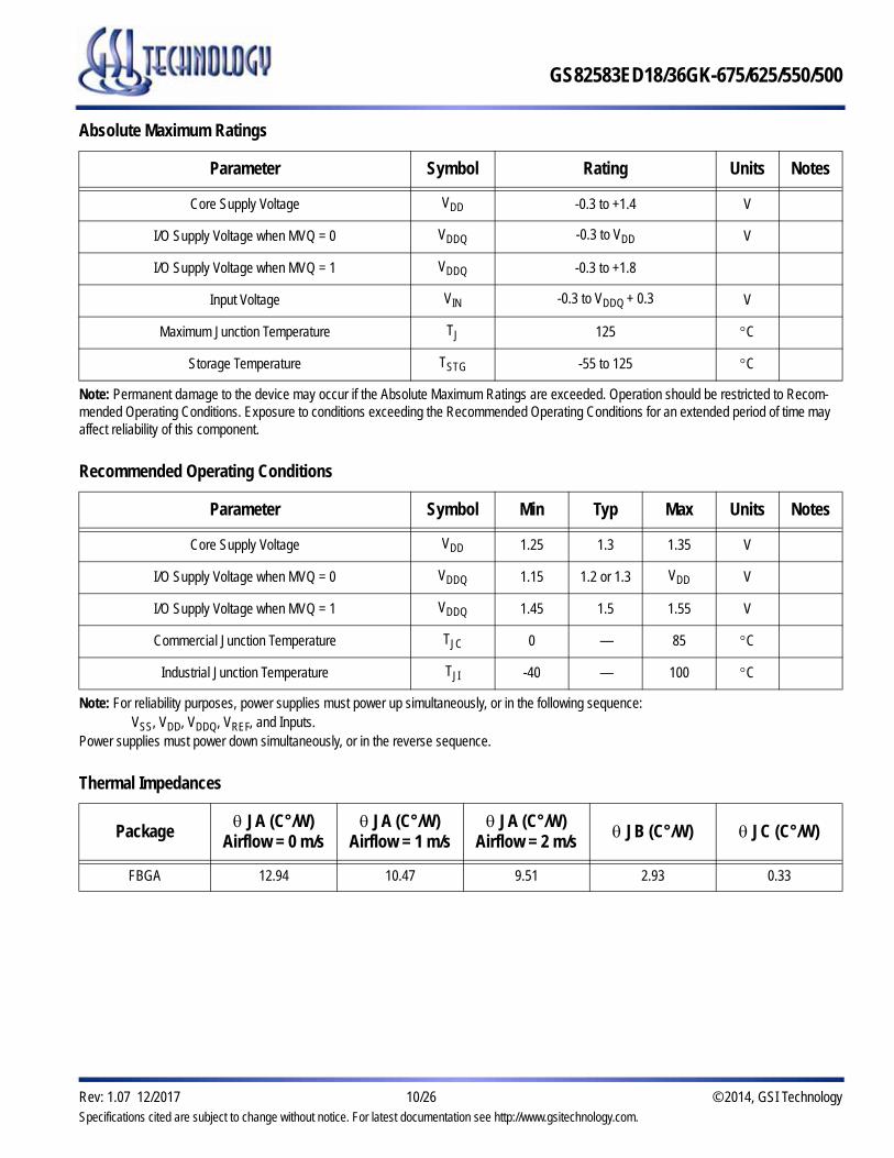
Absolute Maximum Ratings
Parameter Symbol Rating Units Notes
Core Supply Voltage VDD -0.3 to +1.4 V
I/O Supply Voltage when MVQ = 0 VDDQ -0.3 to VDD V
I/O Supply Voltage when MVQ = 1 VDDQ -0.3 to +1.8
Input Voltage VIN -0.3 to VDDQ + 0.3 V
Maximum Junction Temperature TJ 125 C
Storage Temperature TSTG -55 to 125 C
Note: Permanent damage to the device may occur if the Absolute Maximum Ratings are exceeded. Operation should be restricted to Recom-mended Operating Conditions. Exposure to conditions exceeding the Recommended Operating Conditions for an extended period of time may affect reliability of this component.
Recommended Operating Conditions
Parameter Symbol Min Typ Max Units Notes
Core Supply Voltage VDD 1.25 1.3 1.35 V
I/O Supply Voltage when MVQ = 0 VDDQ 1.15 1.2 or 1.3 VDD V
I/O Supply Voltage when MVQ = 1 VDDQ 1.45 1.5 1.55 V
Commercial Junction Temperature TJC 0 — 85 C
Industrial Junction Temperature TJI -40 — 100 C
Note: For reliability purposes, power supplies must power up simultaneously, or in the following sequence: VSS, VDD, VDDQ, VREF, and Inputs.
Power supplies must power down simultaneously, or in the reverse sequence.
Thermal Impedances
PackageJA (C°/W)
Airflow = 0 m/s JA (C°/W)
Airflow = 1 m/s JA (C°/W)
Airflow = 2 m/sJB (C°/W) JC (C°/W)
FBGA 12.94 10.47 9.51 2.93 0.33
Specifications cited are subject to change without notice. For latest documentation see http://www.gsitechnology.com.
Rev: 1.07 12/2017 10/26 © 2014, GSI Technology
GS82583ED18/36GK-675/625/550/500
I/O Capacitance
Parameter Symbol Min Max Units Notes
Input Capacitance CIN — 5.0 pF 1, 3
Output Capacitance COUT — 5.5 pF 2, 3
Notes: 1. VIN = VDDQ/2.
2. VOUT = VDDQ/2.
3. TA = 25C, f = 1 MHz.
Input Electrical Characteristics - 1.2V or 1.3V I/O (MVQ = 0)
Parameter Symbol Min Typ Max Units Notes
DC Input Reference Voltage VREFdc 0.48 * VDDQ 0.50 * VDDQ 0.52 * VDDQ V —
DC Input High Voltage (HS) VIH1dc VREF + 0.08 0.80 * VDDQ VDDQ + 0.15 V 1, 6
DC Input Low Voltage (HS) VIL1dc -0.15 0.20 * VDDQ VREF - 0.08 V 2, 6
DC Input High Voltage (LS) VIH2dc 0.75 * VDDQ VDDQ VDDQ + 0.15 V 7
DC Input Low Voltage (LS) VIL2dc -0.15 0 0.25 * VDDQ V 7
AC Input Reference Voltage VREFac 0.47 * VDDQ 0.50 * VDDQ 0.53 * VDDQ V 3
AC Input High Voltage (HS) VIH1ac VREF + 0.15 0.80 * VDDQ VDDQ + 0.25 V 1, 4~6
AC Input Low Voltage (HS) VIL1ac -0.25 0.20 * VDDQ VREF - 0.15 V 2, 4~6
AC Input High Voltage (LS) VIH2ac VDDQ - 0.2 VDDQ VDDQ + 0.25 V 4, 7
AC Input Low Voltage (LS) VIL2ac -0.25 0 0.2 V 4, 7
Notes:1. “Typ” parameter applies when Controller ROUTH = 40 and SRAM RINH = RINL = 120.
2. “Typ” parameter applies when Controller ROUTL = 40 and SRAM RINH = RINL = 120.
3. VREFac is equal to VREFdc plus noise.
4. VIH max and VIL min apply for pulse widths less than one-quarter of the cycle time.
5. Input rise and fall times must be a minimum of 1V/ns, and within 10% of each other.6. Parameters apply to High Speed Inputs: CK, CK, KD, KD, SA, D, R, W.7. Parameters apply to Low Speed Inputs: RST, DLL, MZT, PZT, MVQ.
Specifications cited are subject to change without notice. For latest documentation see http://www.gsitechnology.com.
Rev: 1.07 12/2017 11/26 © 2014, GSI Technology

GS82583ED18/36GK-675/625/550/500
Input Electrical Characteristics - 1.5V I/O (MVQ = 1)
Parameter Symbol Min Typ Max Units Notes
DC Input Reference Voltage VREFdc 0.48 * VDDQ 0.50 * VDDQ 0.52 * VDDQ V —
DC Input High Voltage (HS) VIH1dc VREF + 0.1 0.80 * VDDQ VDDQ + 0.15 V 1, 6
DC Input Low Voltage (HS) VIL1dc -0.15 0.20 * VDDQ VREF - 0.1 V 2, 6
DC Input High Voltage (LS) VIH2dc 0.75 * VDDQ VDDQ VDDQ + 0.15 V 7
DC Input Low Voltage (LS) VIL2dc -0.15 0 0.25 * VDDQ V 7
AC Input Reference Voltage VREFac 0.47 * VDDQ 0.50 * VDDQ 0.53 * VDDQ V 3
AC Input High Voltage (HS) VIH1ac VREF + 0.2 0.80 * VDDQ VDDQ + 0.25 V 1, 4~6
AC Input Low Voltage (HS) VIL1ac -0.25 0.20 * VDDQ VREF - 0.2 V 2, 4~6
AC Input High Voltage (LS) VIH2ac VDDQ - 0.2 VDDQ VDDQ + 0.25 V 4, 7
AC Input Low Voltage (LS) VIL2ac -0.25 0 0.2 V 4, 7
Notes:1. “Typ” parameter applies when Controller ROUTH = 40 and SRAM RINH = RINL = 120.
2. “Typ” parameter applies when Controller ROUTL = 40 and SRAM RINH = RINL = 120.
3. VREFac is equal to VREFdc plus noise.
4. VIH max and VIL min apply for pulse widths less than one-quarter of the cycle time.
5. Input rise and fall times must be a minimum of 1V/ns, and within 10% of each other.6. Parameters apply to High Speed Inputs: CK, CK, KD, KD, SA, D, R, W.7. Parameters apply to Low Speed Inputs: RST, DLL, MZT, PZT, MVQ.
Output Electrical Characteristics
Parameter Symbol Min Typ Max Units Notes
DC Output High Voltage VOHdc — 0.80 * VDDQ VDDQ + 0.15 V 1, 3
DC Output Low Voltage VOLdc -0.15 0.20 * VDDQ — V 2, 3
AC Output High Voltage VOHac — 0.80 * VDDQ VDDQ + 0.25 V 1, 3
AC Output Low Voltage VOLac -0.25 0.20 * VDDQ — V 2, 3
Note:1. “Typ” parameter applies when SRAM ROUTH = 40 and Controller RINH = RINL = 120.
2. “Typ” parameter applies when SRAM ROUTL = 40 and Controller RINH = RINL = 120.
3. Parameters apply to: CQ, CQ, Q, QVLD.
Specifications cited are subject to change without notice. For latest documentation see http://www.gsitechnology.com.
Rev: 1.07 12/2017 12/26 © 2014, GSI Technology

GS82583ED18/36GK-675/625/550/500
Leakage Currents
Parameter Symbol Min Max Units Notes
Input Leakage Current
ILI1 -2 2 uA 1, 2
ILI2 -20 2 uA 1, 3
ILI3 -2 20 uA 1, 4
Output Leakage Current ILO -2 2 uA 5, 6
Notes:1. VIN = VSS to VDDQ.
2. Parameters apply to CK, CK, KD, KD, SA, D, R, W when ODT is disabled.Parameters apply to MZT, PZT, MVQ.
3. Parameters apply to DLL, TMS, TDI (weakly pulled up).4. Parameters apply to RST, TCK (weakly pulled down).5. VOUT = VSS to VDDQ.
6. Parameters apply to CQ, CQ, Q, QVLD, TDO.
Operating Currents
Parameter Symbol VDD (nom) 500 MHz 550 MHz 625 MHz 675 MHz Units
x18 Operating Current IDD 1.3V 1200 1300 1450 1550 mA
x36 Operating Current IDD 1.3V 1360 1480 1660 1780 mA
Notes:1. IOUT = 0 mA; VIN = VIH or VIL.
2. Applies at 100% alternating Reads and Writes.
Specifications cited are subject to change without notice. For latest documentation see http://www.gsitechnology.com.
Rev: 1.07 12/2017 13/26 © 2014, GSI Technology

GS82583ED18/36GK-675/625/550/500
AC Test Conditions - 1.2V I/O (MVQ = 0)
Parameter Symbol Conditions Units
Core Supply Voltage VDD 1.25 to 1.35 V
I/O Supply Voltage VDDQ 1.15 to 1.25 V
Input Reference Voltage VREF 0.6 V
Input High Level VIH 0.9 V
Input Low Level VIL 0.3 V
Input Rise and Fall Time — 2.0 V/ns
Input and Output Reference Level — 0.6 V
Note: Output Load Conditions RQ = 200. Refer to figure below.
AC Test Conditions - 1.5V I/O (MVQ = 1)
Parameter Symbol Conditions Units
Core Supply Voltage VDD 1.25 to 1.35 V
I/O Supply Voltage VDDQ 1.45 to 1.55 V
Input Reference Voltage VREF 0.75 V
Input High Level VIH 1.25 V
Input Low Level VIL 0.25 V
Input Rise and Fall Time — 2.0 V/ns
Input and Output Reference Level — 0.75 V
Note: Output Load Conditions RQ = 200. Refer to figure below.
AC Test Output Load
50 VDDQ/250
Output
5 pF
Specifications cited are subject to change without notice. For latest documentation see http://www.gsitechnology.com.
Rev: 1.07 12/2017 14/26 © 2014, GSI Technology
GS82583ED18/36GK-675/625/550/500
AC Timing Specifications (independent of device speed grade)
Parameter Symbol Min Max Units Notes
Input Clock Timing
Clk High Pulse Width tKHKL 0.45 — cycles 1
Clk Low Pulse Width tKLKH 0.45 — cycles 1
Clk High to Clk High tKHKH 0.45 0.55 cycles 2
Clk High to Write Data Clk High tKHKDH -200 +200 ps 3
Clk Cycle-to-Cycle Jitter tKJITcc — 60 ps 1,4,5
DLL Lock Time tKlock 65,536 — cycles 6
Clk Static to DLL Reset tKreset 30 — ns 7,12
Output Timing
Clk High to Output Valid / Hold tKHQV/X -0.4 +0.4 ns 8
Clk High to Echo Clock High tKHCQH -0.4 +0.4 ns 9
Echo Clk High to Output Valid / Hold tCQHQV/X -150 +150 ps 10,12
Echo Clk High to Echo Clock High tCQHCQH tKHKH (min) - 100 tKHKH (max) + 100 ps 11,12
Notes:All parameters are measured from the mid-point of the object signal to the mid-point of the reference signal.1. Parameters apply to CK, CK, KD, KD.2. Parameter specifiesCK CK and KD KD requirements.3. Parameter specifies CK KD and CK KD requirements.4. Parameter specifies Cycle-to-Cycle (C2C) Jitter (i.e. the maximum variation from clock rising edge to the next clock rising edge).
As such, it limits Period Jitter (i.e. the maximum variation in clock cycle time from nominal) to 30ps. And as such, it limits Absolute Jitter (i.e. the maximum variation in clock rising edge from its nominal position) to 15ps.
5. The device can tolerated C2C Jitter greater than 60ps, up to a maximum of 200ps. However, when using a device from a particular speed grade, tKHKH (min) of that speed grade must be derated (increased) by half the difference between the actual C2C Jitter and 60ps. For example, if the actual C2C Jitter is 100ps, then tKHKH (min) for the -675 speed grade is derated to 1.5ns (1.48ns + 0.5*(100ps - 60ps)).
6. VDD slew rate must be < 0.1V DC per 50ns for DLL lock retention. DLL lock time begins once VDD and input clock are stable.
7. Parameter applies to CK.8. Parameters apply to Q, and are referenced to CK.9. Parameter specifies CK CQ timing.10. Parameters apply to Q, QVLD and are referenced to CQ & CQ.11. Parameter specifies CQ CQ timing.12. Parameters are not tested. They are guaranteed by design, and verified through extensive corner-lot characterization.
Specifications cited are subject to change without notice. For latest documentation see http://www.gsitechnology.com.
Rev: 1.07 12/2017 15/26 © 2014, GSI Technology

GS82583ED18/36GK-675/625/550/500
AC Timing Specifications (variable with device speed grade)
Parameter Symbol–675 –625 –550 –500
Units NotesMin Max Min Max Min Max Min Max
Input Clock Timing
Clk Cycle Time tKHKH 1.48 6.0 1.6 6.0 1.8 6.0 2.0 6.0 ns 1
Input Setup & Hold Timing
Input Valid to Clk High tIVKH 150 — 160 — 180 — 200 — ps2
Clk High to Input Hold tKHIX 150 — 160 — 180 — 200 — ps
Notes:All parameters are measured from the mid-point of the object signal to the mid-point of the reference signal.1. Parameters apply to CK, CK, KD, KD.2. Parameters apply to SA, and are referenced to CK.
Parameters apply to R, W, and are referenced to CK.Parameters apply to D, and are referenced to KD & KD.
Specifications cited are subject to change without notice. For latest documentation see http://www.gsitechnology.com.
Rev: 1.07 12/2017 16/26 © 2014, GSI Technology

GS82583ED18/36GK-675/625/550/500
Read and Write Timing Diagram
tKHIXtIVKH
tKHIXtIVKH
tKHKDH tKHKDH
A6
CK
CK
SA
Q
Read Write Read NOP NOP Write Read Write Read Write NOP
A2 A3
W
A7
D
A8
Q11 Q12 Q13 Q14 Q31 Q32 Q33 Q34
D21 D22 D23 D24 D41 D42 D43 D44 D61 D62 D63 D64 D81
QVLD
KD
KD
R
A4 A5
tKHIXtIVKH tKHIXtIVKH
tKHKH tKHKL tKLKH tKHKH
tKHKH tKHKL tKLKH tKHKH
Q51
tKHQV tKHQX
CQ
CQ
tCQHQVtCQHQV
tCQHQX
tCQHQV
tCQHQX tCQHQX
tCQHCQH
tKHCQH
Q52 Q53
A1
Specifications cited are subject to change without notice. For latest documentation see http://www.gsitechnology.com.
Rev: 1.07 12/2017 17/26 © 2014, GSI Technology

GS82583ED18/36GK-675/625/550/500
JTAG Test Mode DescriptionThese devices provide a JTAG Test Access Port (TAP) and Boundary Scan interface using a limited set of IEEE std. 1149.1 functions. This test mode is intended to provide a mechanism for testing the interconnect between master (processor, controller, etc.), SRAM, other components, and the printed circuit board. In conformance with a subset of IEEE std. 1149.1, these devices contain a TAP Controller and multiple TAP Registers. The TAP Registers consist of one Instruction Register and multiple Data Registers.
The TAP consists of the following four signals:
Pin Pin Name I/O Description
TCK Test Clock I Induces (clocks) TAP Controller state transitions.
TMS Test Mode Select IInputs commands to the TAP Controller.
Sampled on the rising edge of TCK.
TDI Test Data In IInputs data serially to the TAP Registers.
Sampled on the rising edge of TCK.
TDO Test Data Out OOutputs data serially from the TAP Registers.
Driven from the falling edge of TCK.
Concurrent TAP and Normal SRAM Operation
According to IEEE std. 1149.1, most public TAP Instructions do not disrupt normal device operation. In these devices, the only exceptions are EXTEST and SAMPLE-Z. See the Tap Registers section for more information.
Disabling the TAP
When JTAG is not used, TCK should be tied Low to prevent clocking the SRAM. TMS and TDI should either be tied High through a pull-up resistor or left unconnected. TDO should be left unconnected.
JTAG DC Operating Conditions
Parameter Symbol Min Max Units Notes
JTAG Input High Voltage VTIH 0.75 * VDDQ VDDQ + 0.15 V 1
JTAG Input Low Voltage VTIL –0.15 0.25 * VDDQ V 1
JTAG Output High Voltage VTOH VDDQ – 0.2 — V 2, 3
JTAG Output Low Voltage VTOL — 0.2 V 2, 4
Notes:1. Parameters apply to TCK, TMS, and TDI.2. Parameters apply to TDO.3. ITOH = –2.0 mA.
4. ITOL = 2.0 mA.
Specifications cited are subject to change without notice. For latest documentation see http://www.gsitechnology.com.
Rev: 1.07 12/2017 18/26 © 2014, GSI Technology

GS82583ED18/36GK-675/625/550/500
JTAG AC Timing Specifications
Parameter Symbol Min Max Units
TCK Cycle Time tTHTH 50 — ns
TCK High Pulse Width tTHTL 20 — ns
TCK Low Pulse Width tTLTH 20 — ns
TMS Setup Time tMVTH 10 — ns
TMS Hold Time tTHMX 10 — ns
TDI Setup Time tDVTH 10 — ns
TDI Hold Time tTHDX 10 — ns
Capture Setup Time (Address, Control, Data, Clock) tCS 10 — ns
Capture Hold Time (Address, Control, Data, Clock) tCH 10 — ns
TCK Low to TDO Valid tTLQV — 10 ns
TCK Low to TDO Hold tTLQX 0 — ns
JTAG Timing Diagram
tTHTL tTLTH tTHTH
tTHMXtMVTH
tTHDXtDVTH
tTLQV
tTLQX
TCK
TMS
TDITDI
TDO
Specifications cited are subject to change without notice. For latest documentation see http://www.gsitechnology.com.
Rev: 1.07 12/2017 19/26 © 2014, GSI Technology

GS82583ED18/36GK-675/625/550/500
TAP ControllerThe TAP Controller is a 16-state state machine that controls access to the various TAP Registers and executes the operations associated with each TAP Instruction. State transitions are controlled by TMS and occur on the rising edge of TCK. The TAP Controller enters the Test-Logic Reset state in one of two ways:
1. At power up.2. When a logic 1 is applied to TMS for at least 5 consecutive rising edges of TCK.
The TDI input receiver is sampled only when the TAP Controller is in either the Shift-IR state or the Shift-DR state.The TDO output driver is enabled only when the TAP Controller is in either the Shift-IR state or the Shift-DR state.
TAP Controller State Diagram
Test-Logic Reset
Run-Test / Idle Select DR-Scan Select IR-Scan
Capture-DR Capture-IR
Shift-DR Shift-IR
Exit1-DR Exit1-IR
Pause-DR Pause-IR
Exit2-DR Exit2-IR
Update-DR Update-IR
1
0
1
0
1
0
0
0
1
1
0
1
0
1
0
0
1
1
1
0
1
0
1
0
0
0
1
1
0
1
0
1
Specifications cited are subject to change without notice. For latest documentation see http://www.gsitechnology.com.
Rev: 1.07 12/2017 20/26 © 2014, GSI Technology
GS82583ED18/36GK-675/625/550/500
TAP RegistersTAP Registers are serial shift registers that capture serial input data (from TDI) on the rising edge of TCK, and drive serial output data (to TDO) on the subsequent falling edge of TCK. They are divided into two groups: Instruction Registers (IR), which are manipulated via the IR states in the TAP Controller, and Data Registers (DR), which are manipulated via the DR states in the TAP Controller.
Instruction Register (IR - 3 bits)
The Instruction Register stores the various TAP Instructions supported by SRAM. It is loaded with the IDCODE instruction (logic 001) at power-up, and when the TAP Controller is in the Test-Logic Reset and Capture-IR states. It is inserted between TDI and TDO when the TAP Controller is in the Shift-IR state, at which time it can be loaded with a new instruction. However, newly loaded instructions are not executed until the TAP Controller has reached the Update-IR state.
The Instruction Register is 3 bits wide, and is encoded as follows:
Code(2:0)
Instruction Description
000 EXTEST
Loads the logic states of all signals composing the SRAM I/O ring into the Boundary Scan Register when the TAP Controller is in the Capture-DR state, and inserts the Boundary Scan Register between TDI and TDO when the TAP Controller is in the Shift-DR state.Also transfers the contents of the Boundary Scan Register associated with output signals (Q, QVLD, CQ, CQ) directly to their corresponding output pins. However, newly loaded Boundary Scan Register contents do not appear at the output pins until the TAP Controller has reached the Update-DR state.Also disables all ODT.See the Boundary Scan Register description for more information.
001 IDCODE
Loads a predefined device- and manufacturer-specific identification code into the ID Register when the TAP Controller is in the Capture-DR state, and inserts the ID Register between TDI and TDO when the TAP Controller is in the Shift-DR state.See the ID Register description for more information.
010 SAMPLE-Z
Loads the logic states of all signals composing the SRAM I/O ring into the Boundary Scan Register when the TAP Controller is in the Capture-DR state, and inserts the Boundary Scan Register between TDI and TDO when the TAP Controller is in the Shift-DR state.Also disables all ODT.Also forces Q output drivers to a High-Z state.See the Boundary Scan Register description for more information.
011 PRIVATE Reserved for manufacturer use only.
100 SAMPLE
Loads the logic states of all signals composing the SRAM I/O ring into the Boundary Scan Register when the TAP Controller is in the Capture-DR state, and inserts the Boundary Scan Register between TDI and TDO when the TAP Controller is in the Shift-DR state.See the Boundary Scan Register description for more information.
101 PRIVATE Reserved for manufacturer use only.
110 PRIVATE Reserved for manufacturer use only.
111 BYPASSLoads a logic 0 into the Bypass Register when the TAP Controller is in the Capture-DR state, and inserts the Bypass Register between TDI and TDO when the TAP Controller is in the Shift-DR state.See the Bypass Register description for more information.
Specifications cited are subject to change without notice. For latest documentation see http://www.gsitechnology.com.
Rev: 1.07 12/2017 21/26 © 2014, GSI Technology

GS82583ED18/36GK-675/625/550/500
Bypass Register (DR - 1 bit)
The Bypass Register is one bit wide, and provides the minimum length serial path between TDI and TDO. It is loaded with a logic 0 when the BYPASS instruction has been loaded in the Instruction Register and the TAP Controller is in the Capture-DR state. It is inserted between TDI and TDO when the BYPASS instruction has been loaded into the Instruction Register and the TAP Controller is in the Shift-DR state.
ID Register (DR - 32 bits)
The ID Register is loaded with a predetermined device- and manufacturer-specific identification code when the IDCODE instruction has been loaded into the Instruction Register and the TAP Controller is in the Capture-DR state. It is inserted between TDI and TDO when the IDCODE instruction has been loaded into the Instruction Register and the TAP Controller is in the Shift-DR state.
The ID Register is 32 bits wide, and is encoded as follows:
See BSDL Model(31:12)
GSI ID(11:1)
Start Bit(0)
XXXX XXXX XXXX XXXX XXXX 0001 1011 001 1
Bit 0 is the LSB of the ID Register, and Bit 31 is the MSB. When the ID Register is selected, TDI serially shifts data into the MSB, and the LSB serially shifts data out through TDO.
Boundary Scan Register (DR - 129 bits)
The Boundary Scan Register is equal in length to the number of active signal connections to the SRAM (excluding the TAP pins) plus a number of place holder locations reserved for functional and/or density upgrades. It is loaded with the logic states of all signals composing the SRAM’s I/O ring when the EXTEST, SAMPLE, or SAMPLE-Z instruction has been loaded into the Instruction Register and the TAP Controller is in the Capture-DR state. It is inserted between TDI and TDO when the EXTEST, SAMPLE, or SAMPLE-Z instruction has been loaded into the Instruction Register and the TAP Controller is in the Shift-DR state.
Additionally, the contents of the Boundary Scan Register associated with the SRAM outputs (Q, QVLD, CQ, CQ) are driven directly to the corresponding SRAM output pins when the EXTEST instruction is selected. However, after the EXTEST instruction has been selected, any new data loaded into Boundary Scan Register when the TAP Controller is in the Shift-DR state does not appear at the output pins until the TAP Controller has reached the Update-DR state.
The value captured in the boundary scan register for NU pins is determined by the external pin state. The value captured in the boundary scan register for NC pins is 0 regardless of the external pin state. The value captured in the Internal Cell (Bit 129) is 1.
Output Driver State During EXTEST
EXTEST allows the Internal Cell (Bit 129) in the Boundary Scan Register to control the state of Q drivers. That is, when Bit 129 = 1, Q drivers are enabled (i.e., driving High or Low), and when Bit 129 = 0, Q drivers are disabled (i.e., forced to High-Z state). See the Boundary Scan Register section for more information.
ODT State During EXTEST and SAMPLE-Z
ODT on all inputs is disabled during EXTEST and SAMPLE-Z.
Specifications cited are subject to change without notice. For latest documentation see http://www.gsitechnology.com.
Rev: 1.07 12/2017 22/26 © 2014, GSI Technology

GS82583ED18/36GK-675/625/550/500
Boundary Scan Register Bit Order Assignment
The table below depicts the order in which the bits are arranged in the Boundary Scan Register. Bit 1 is the LSB and Bit 129 is the MSB. When the Boundary Scan Register is selected, TDI serially shifts data into the MSB, and the LSB serially shifts data out through TDO.
Bit Pad Bit Pad Bit Pad Bit Pad Bit Pad
1 7L 29 12F 57 12W 85 1T 113 1C
2 7K 30 11G 58 10W 86 4R 114 3C
3 9L 31 13G 59 8V 87 2R 115 2B
4 9K 32 10G 60 9U 88 3P 116 4B
5 8J 33 12G 61 8T 89 1P 117 5A
6 7H 34 11H 62 9R 90 4P 118 6A
7 9H 35 13H 63 8P 91 2P 119 6B
8 7G 36 10J 64 9N 92 3N 120 6C
9 8G 37 12J 65 8M 93 1N 121 5D
10 9F 38 13K 66 6M 94 4M 122 6E
11 8E 39 13L 67 7N 95 2M 123 5F
12 7D 40 11L 68 5N 96 3L 124 6G
13 9D 41 12M 69 7P 97 1L 125 5H
14 8C 42 10M 70 6P 98 1K 126 6J
15 7B 43 13N 71 5R 99 2J 127 5K
16 8B 44 11N 72 6T 100 4J 128 5L
17 9B 45 12P 73 7U 101 1H 129 Internal
18 7A 46 10P 74 5U 102 3H
19 9A 47 13P 75 6V 103 2G
20 10B 48 11P 76 6W 104 4G
21 12B 49 12R 77 7Y 105 1G
22 11C 50 10R 78 4W 106 3G
23 13C 51 13T 79 2W 107 2F
24 10D 52 11T 80 3V 108 4F
25 12D 53 12U 81 1V 109 1E
26 11E 54 10U 82 4U 110 3E
27 13E 55 13V 83 2U 111 2D
28 10F 56 11V 84 3T 112 4D
Specifications cited are subject to change without notice. For latest documentation see http://www.gsitechnology.com.
Rev: 1.07 12/2017 23/26 © 2014, GSI Technology

GS82583ED18/36GK-675/625/550/500
260-Pin BGA Package Drawing (Package GK)
Ball Pitch:
Ball Diameter:
Substrate Thickness:
Mold Thickness:
13 12 11 10 9 8 7 6 5 4 3
A
B
C
D
E
F
G
H
J
K
L
M
N
P
R
T
U
V
W
13.20 0.05
14.00 0.05
22.0
0
0.0
5
17.4
0
0.0
5
PIN #1 CORNER
2 1
Y
SEATING PLANE
HEAT SPREADER
1.00
12.0019
.00
1.00
A
B
0.05(4X)
1.00
0.60
0.51
—
0.50
+ 0
.03
2.10
+ 0
.2/–
0.3
0.40
~0.
60
C
0.06
0.10
C
//
1.0
9 R
EF
0.51
RE
F
0.05 4–R0.5 (MAX)
Ø0.50~Ø0.70(260x)
Ø0.08 SØ0.22 S
CC A S B S
0.15
C
Specifications cited are subject to change without notice. For latest documentation see http://www.gsitechnology.com.
Rev: 1.07 12/2017 24/26 © 2014, GSI Technology

GS82583ED18/36GK-675/625/550/500
Ordering Information — GSI SigmaQuad-IIIe SRAM
Org Part Number Type PackageSpeed (MHz)
TA
16M x 18 GS82583ED18GK-675 SigmaQuad-IIIe B4 ROHS-Compliant 260-Pin BGA 675 C
16M x 18 GS82583ED18GK-625 SigmaQuad-IIIe B4 ROHS-Compliant 260-Pin BGA 625 C
16M x 18 GS82583ED18GK-550 SigmaQuad-IIIe B4 ROHS-Compliant 260-Pin BGA 550 C
16M x 18 GS82583ED18GK-500 SigmaQuad-IIIe B4 ROHS-Compliant 260-Pin BGA 500 C
16M x 18 GS82583ED18GK-675I SigmaQuad-IIIe B4 ROHS-Compliant 260-Pin BGA 675 I
16M x 18 GS82583ED18GK-625I SigmaQuad-IIIe B4 ROHS-Compliant 260-Pin BGA 625 I
16M x 18 GS82583ED18GK-550I SigmaQuad-IIIe B4 ROHS-Compliant 260-Pin BGA 550 I
16M x 18 GS82583ED18GK-500I SigmaQuad-IIIe B4 ROHS-Compliant 260-Pin BGA 500 I
8M x 36 GS82583ED36GK-675 SigmaQuad-IIIe B4 ROHS-Compliant 260-Pin BGA 675 C
8M x 36 GS82583ED36GK-625 SigmaQuad-IIIe B4 ROHS-Compliant 260-Pin BGA 625 C
8M x 36 GS82583ED36GK-550 SigmaQuad-IIIe B4 ROHS-Compliant 260-Pin BGA 550 C
8M x 36 GS82583ED36GK-500 SigmaQuad-IIIe B4 ROHS-Compliant 260-Pin BGA 500 C
8M x 36 GS82583ED36GK-675I SigmaQuad-IIIe B4 ROHS-Compliant 260-Pin BGA 675 I
8M x 36 GS82583ED36GK-625I SigmaQuad-IIIe B4 ROHS-Compliant 260-Pin BGA 625 I
8M x 36 GS82583ED36GK-550I SigmaQuad-IIIe B4 ROHS-Compliant 260-Pin BGA 550 I
8M x 36 GS82583ED36GK-500I SigmaQuad-IIIe B4 ROHS-Compliant 260-Pin BGA 500 I
Note: C = Commercial Temperature Range. I = Industrial Temperature Range.
Specifications cited are subject to change without notice. For latest documentation see http://www.gsitechnology.com.
Rev: 1.07 12/2017 25/26 © 2014, GSI Technology
GS82583ED18/36GK-675/625/550/500
Revision History
Rev. CodeTypes of Changes Format or Content
Revisions
GS82583ED1836GK_r1_01 — • Initial public release.
GS82583ED1836GK_r1_02 Content • Removed leaded BGA package support.
GS82583ED1836GK_r1_03 Content• Miscellaneous cleanup.• Corrected write data input latency.
GS82583ED1836GK_r1_04 Content• Changed VDD spec to 1.3V 50mV.• Added package thermal impedances.• Revised tCQHCQH specs.
GS82583ED1836GK_r1_05 Content• Removed Preliminary banner.• Added IDD specs.
GS82583ED1836GK_r1_06 Content • Removed ECCRAM references.
GS82583ED1836GK_r1_07 Content • Changed Junction Temp to Max Junction Temp in AbsMax table
Specifications cited are subject to change without notice. For latest documentation see http://www.gsitechnology.com.
Rev: 1.07 12/2017 26/26 © 2014, GSI Technology