Embed Size (px)
Citation preview
A2S56D20CTPA2S56D30CTPA2S56D40CTP
256Mb DDR SDRAM Specification256Mb DDR SDRAM Specification256Mb DDR SDRAM Specification256Mb DDR SDRAM Specification256Mb DDR SDRAM Specification
Powerchip Semiconductor Corp.
No.12, Li-Hsin Rd.1, Science-based Industrial Park, Hsin-Chu
Taiwan, R.O.C.
TEL: 886-3-5795000
FAX: 886-3-5792168
Jun.2004 Rev.1.0
256Mb DDR Synchronous DRAM256Mb DDR Synchronous DRAM256Mb DDR Synchronous DRAM256Mb DDR Synchronous DRAM256Mb DDR Synchronous DRAMA2S56D20CTP (4-bank x 16,777,216 - word x 4-bit)A2S56D30CTP (4-bank x 8,388,608 - word x 8-bit)A2S56D40CTP (4-bank x 4,194,304 - word x 16-bit)Powerchip Semiconductor Corp.
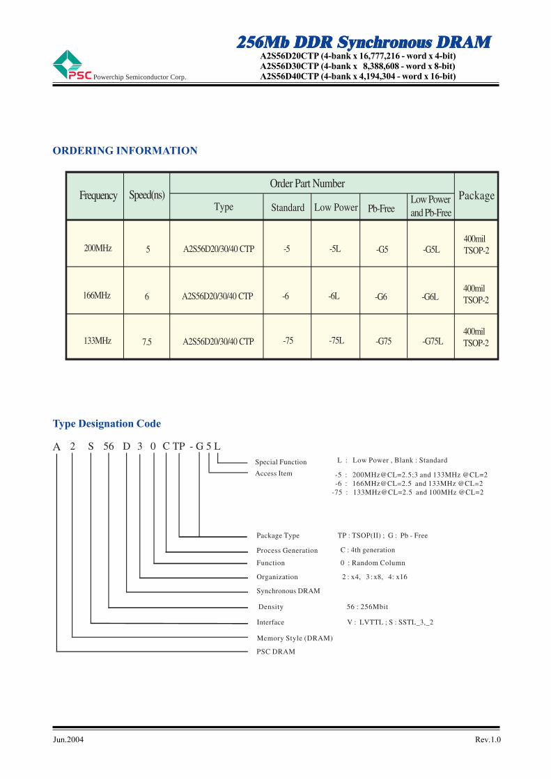
FrequencyOrder Part Number
PackagePb-Free
Low Power and Pb-Free
400mil TSOP-2
Type Standard Low Power
400mil TSOP-2
Speed(ns)
-5 -5L -G5 -G5L200MHz A2S56D20/30/40 CTP 5
-6 -6L -G6 -G6L166MHz A2S56D20/30/40 CTP 6
-75 -75L -G75 -G75L133MHz A2S56D20/30/40 CTP 7.5
400mil TSOP-2
2 S 56 D 3 0 TP - G 5 L
Access Item
Package Type TP : TSOP(II) ; G : Pb - Free
Process Generation
Interface V : LVTTL ; S : SSTL_3,_2
Organization 2 : x4, 3 : x8, 4: x16
Synchronous DRAM
Density 56 : 256Mbit
Function 0 : Random Column
PSC DRAM
C
C : 4th generation
Special Function L : Low Power , Blank : Standard
-5 : 200MHz@CL=2.5;3 and 133MHz @CL=2 -6 : 166MHz@CL=2.5 and 133MHz @CL=2 -75 : 133MHz@CL=2.5 and 100MHz @CL=2
A
Memory Style (DRAM)
Type Designation Code
ORDERING INFORMATION
Jun.2004 Rev.1.0
256Mb DDR Synchronous DRAM256Mb DDR Synchronous DRAM256Mb DDR Synchronous DRAM256Mb DDR Synchronous DRAM256Mb DDR Synchronous DRAM
Powerchip Semiconductor Corp.
A2S56D20CTP (4-bank x 16,777,216 - word x 4-bit)A2S56D30CTP (4-bank x 8,388,608 - word x 8-bit)A2S56D40CTP (4-bank x 4,194,304 - word x 16-bit)
DESCRIPTIONA2S56D20CTP is a 4-bank x 16,777,216-word x 4-bit,
A2S56D30CTP is a 4-bank x 8,388,608-word x 8bit,
A2S56D40CTP is a 4-bank x 4,194,304-word x 16bit double
data rate synchronous DRAM , with SSTL_2 interface.
All control and address signals are referenced to the rising
edge of CLK.
256Mb Double Data Rate Synchronous DRAM
A2S56D20/30/40 CTP
Page- 1
- Vdd=Vddq=2.5V ± 0.2V power supply for -6,-75.-Vdd=Vddq=2.6V ± 0.1V power supply for -5.- Double data rate architecture ; two data transfers per clock cycle.- Bidirectional , data strob (DQS) is transmitted/received with data- Differential clock input (CLK and /CLK)- DLL aligns DQ and DQS transitions with CLK transitions edges of DQS- Commands entered on each positive CLK edge ;- Data and data mask referenced to both edges of DQS- 4 bank operation controlled by BA0 , BA1 (Bank Address)- /CAS latency - 2.0 / 2.5/ 3 (programmable) ; Burst length - 2 / 4 / 8 (programmable) Burst type - Sequential / Interleave (programmable)- Auto precharge / All bank precharge controlled by A10- 8192 refresh cycles / 64ms (4 banks concurrent refresh)- Auto refresh and Self refresh- Row address A0-12 / Column address A0-9 , 11(x4) / A0-9(x8)/A0-8(x16)- SSTL_2 Interface- Package 400-mil, 66-pin Thin Small Outline Package (TSOP II) with 0.65mm lead pitch- JEDEC standard for -6 , -75- Intel standard for -5
FEATURES
Input data is registered on both edges of data strob ,
and output data and data strobe are referenced on
both edges of CLK.
The A2S56D20/30/40 CTP achieves very high speed clock
rate up to 200 MHz .
123456789101112131415161718192021222324252627282930313233
666564636261605958575655545352515049484746454443424140393837363534
VDDNC
VDDQNC
DQ0VSSQ
NCNC
VDDQNC
DQ1VSSQ
NCNC
VDDQNCNC
VDDNU/QFC
NC/WE
/CAS/RAS
/CSNC
BA0BA1
A10/APA0A1A2A3
VDD
VSSNCVSSQNCDQ3VDDQNCNCVSSQNCDQ2VDDQNCNCVSSQDQSNCVREFVSSDM/CLKCLKCKENCA12A11A9A8A7A6A5A4VSS
x4
66p
in T
SO
P(II) 4
00
milx
87
5m
il (0.6
5m
m lea
d p
itch)
PIN CONFIGURATION (TOP VIEW)
Jun.2004 Rev.1.0
256Mb DDR Synchronous DRAM256Mb DDR Synchronous DRAM256Mb DDR Synchronous DRAM256Mb DDR Synchronous DRAM256Mb DDR Synchronous DRAMA2S56D20CTP (4-bank x 16,777,216 - word x 4-bit)A2S56D30CTP (4-bank x 8,388,608 - word x 8-bit)A2S56D40CTP (4-bank x 4,194,304 - word x 16-bit)Powerchip Semiconductor Corp.
Page- 2
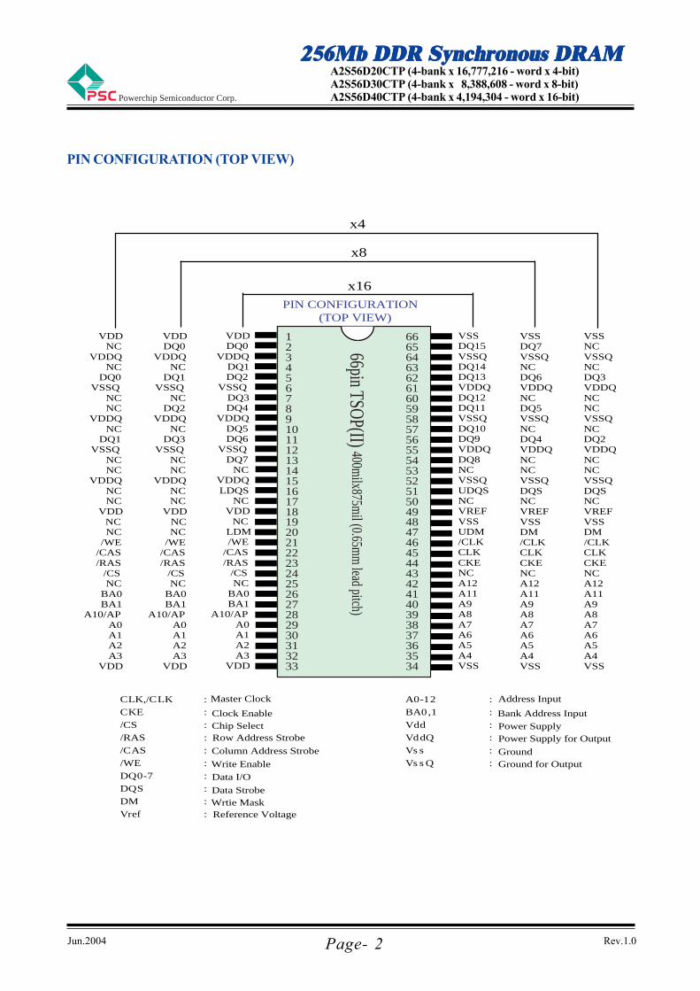
PIN CONFIGURATION (TOP VIEW)
CLK,/CLK : Master Clock
CKE :
/CS :
/RAS :
/CAS :
/WE :
DQ0-7 :
DQS :
DM :
PIN CONFIGURATION (TOP VIEW)
VDDDQ0
VDDQNC
DQ1VSSQ
NCDQ2
VDDQNC
DQ3VSSQ
NCNC
VDDQNCNC
VDDNCNC
/WE/CAS/RAS
/CSNC
BA0BA1
A10/APA0A1A2A3
VDD
VSSDQ7VSSQNCDQ6VDDQNCDQ5VSSQNCDQ4VDDQNCNCVSSQDQSNCVREFVSSDM/CLKCLKCKENCA12A11A9A8A7A6A5A4VSS
VDDNC
VDDQNC
DQ0VSSQ
NCNC
VDDQNC
DQ1VSSQ
NCNC
VDDQNCNC
VDDNCNC
/WE/CAS/RAS
/CSNC
BA0BA1
A10/APA0A1A2A3
VDD
VSSNCVSSQNCDQ3VDDQNCNCVSSQNCDQ2VDDQNCNCVSSQDQSNCVREFVSSDM/CLKCLKCKENCA12A11A9A8A7A6A5A4VSS
x8
A0-12 :
BA0,1 :
Vdd :
VddQ :
Vs s :
Vs s Q :
123456789101112131415161718192021222324252627282930313233
666564636261605958575655545352515049484746454443424140393837363534
66pin TSOP(II) 400milx875m
il (0.65mm
lead pitch)
x16
VDDDQ0
VDDQDQ1DQ2
VSSQDQ3DQ4
VDDQDQ5DQ6
VSSQDQ7
NCVDDQLDQS
NCVDD
NCLDM/WE
/CAS/RAS
/CSNC
BA0BA1
A10/APA0A1A2A3
VDD
VSSDQ15VSSQDQ14DQ13VDDQDQ12DQ11VSSQDQ10DQ9VDDQDQ8NCVSSQUDQSNCVREFVSSUDM/CLKCLKCKENCA12A11A9A8A7A6A5A4VSS
x4
Clock EnableChip SelectRow Address Strobe
Column Address Strobe
Write Enable
Data I/O
Data StrobeWrtie Mask
Vref : Reference Voltage
Address Input
Bank Address Input
Power SupplyPower Supply for Output
GroundGround for Output
Jun.2004 Rev.1.0
256Mb DDR Synchronous DRAM256Mb DDR Synchronous DRAM256Mb DDR Synchronous DRAM256Mb DDR Synchronous DRAM256Mb DDR Synchronous DRAM
Powerchip Semiconductor Corp.
A2S56D20CTP (4-bank x 16,777,216 - word x 4-bit)A2S56D30CTP (4-bank x 8,388,608 - word x 8-bit)A2S56D40CTP (4-bank x 4,194,304 - word x 16-bit)
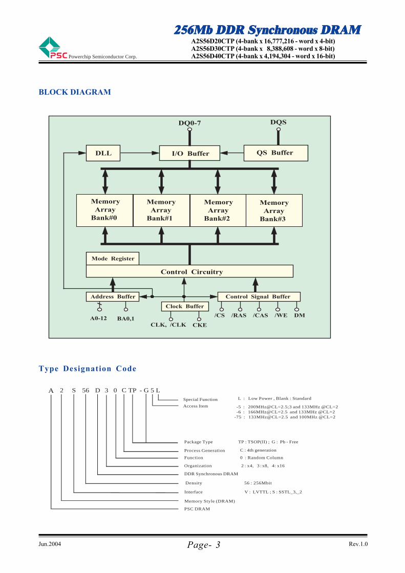
Memory ArrayBank#0
Memory ArrayBank#1
Memory ArrayBank#2
Memory ArrayBank#3
Mode Register
Control Circuitry
Address Buffer
Clock Buffer
Control Signal Buffer
CLK, /CLK CKEA0-12 BA0,1
/CS /RAS /CAS /WE DM
DLL I/O Buffer
DQSDQ0-7
QS Buffer
2 S 56 D 3 0 TP - G 5 L
Access Item
Package Type TP : TSOP(II) ; G : Pb - Free
Process Generation
Interface V : LVTTL ; S : SSTL_3,_2
Organization 2 : x4, 3 : x8, 4: x16
DDR Synchronous DRAM
Density 56 : 256Mbit
Function 0 : Random Column
PSC DRAM
C
C : 4th generation
Special Function L : Low Power , Blank : Standard
-5 : 200MHz@CL=2.5;3 and 133MHz @CL=2 -6 : 166MHz@CL=2.5 and 133MHz @CL=2 -75 : 133MHz@CL=2.5 and 100MHz @CL=2
A
Memory Style (DRAM)
Page- 3
BLOCK DIAGRAM
Type Designation Code
Jun.2004 Rev.1.0
256Mb DDR Synchronous DRAM256Mb DDR Synchronous DRAM256Mb DDR Synchronous DRAM256Mb DDR Synchronous DRAM256Mb DDR Synchronous DRAMA2S56D20CTP (4-bank x 16,777,216 - word x 4-bit)A2S56D30CTP (4-bank x 8,388,608 - word x 8-bit)A2S56D40CTP (4-bank x 4,194,304 - word x 16-bit)Powerchip Semiconductor Corp.
Page- 4
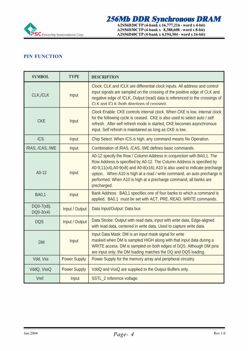
PIN FUNCTION
CLK,/CLK Input
Clock: CLK and /CLK are differential clock inputs. All address and control input signals are sampled on the crossing of the positive edge of CLK and negative edge of /CLK. Output (read) data is referenced to the crossings of CLK and /CLK (both directions of crossing).
CKE Input
Clock Enable: CKE controls internal clock. When CKE is low, internal clock for the following cycle is ceased. CKE is also used to select auto / self refresh. After self refresh mode is started, CKE becomes asynchronous input. Self refresh is maintained as long as CKE is low.
/CS Input Chip Select: When /CS is high, any command means No Operation.
/RAS, /CAS, /WE Input Combination of /RAS, /CAS, /WE defines basic commands.
A0-12 Input
A0-12 specify the Row / Column Address in conjunction with BA0,1. The Row Address is specified by A0-12. The Column Address is specified by A0-9,11(x4),A0-9(x8) and A0-8(x16).
A10 is also used to indicate precharge option. When A10 is high at a read / write command, an auto precharge is performed. When A10 is high at a precharge command, all banks are precharged.
BA0,1 Input
DQ0-7(x8),DQ0-3(x4)
Input / Output
DQS
Vdd, Vss Power Supply Power Supply for the memory array and peripheral circuitry.
VddQ, VssQ Power Supply VddQ and VssQ are supplied to the Output Buffers only.
Bank Address: BA0,1 specifies one of four banks to which a command is applied. BA0,1 must be set with ACT, PRE, READ, WRITE commands.
Data Input/Output: Data bus
Data Strobe: Output with read data, input with write data. Edge-aligned with read data, centered in write data. Used to capture write data.
DM Input
Input Data Mask: DM is an input mask signal for write masked when DM is sampled HIGH along with that input data during a WRITE access. DM is sampled on both edges of DQS. Although DM pins are input only, the DM loading matches the DQ and DQS loading.
Input / Output
Vref Input SSTL_2 reference voltage.
SYMBOL TYPE DESCRIPTION
Jun.2004 Rev.1.0
256Mb DDR Synchronous DRAM256Mb DDR Synchronous DRAM256Mb DDR Synchronous DRAM256Mb DDR Synchronous DRAM256Mb DDR Synchronous DRAM
Powerchip Semiconductor Corp.
A2S56D20CTP (4-bank x 16,777,216 - word x 4-bit)A2S56D30CTP (4-bank x 8,388,608 - word x 8-bit)A2S56D40CTP (4-bank x 4,194,304 - word x 16-bit)
Page- 5
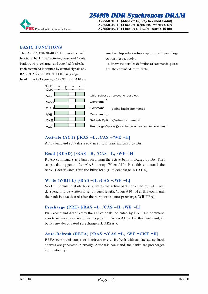
Activate (ACT) [/RAS =L, /CAS =/WE =H]ACT command activates a row in an idle bank indicated by BA.
Read (READ) [/RAS =H, /CAS =L, /WE =H]READ command starts burst read from the active bank indicated by BA. First
output data appears after /CAS latency. When A10 =H at this command, the
bank is deactivated after the burst read (auto-precharge, READA).
Write (WRITE) [/RAS =H, /CAS =/WE =L]WRITE command starts burst write to the active bank indicated by BA. Total
data length to be written is set by burst length. When A10 =H at this command,
the bank is deactivated after the burst write (auto-precharge, WRITEA).
Precharge (PRE) [/RAS =L, /CAS =H, /WE =L]PRE command deactivates the active bank indicated by BA. This command
also terminates burst read / write operation. When A10 =H at this command, all
banks are deactivated (precharge all, PREA ).
Auto-Refresh (REFA) [/RAS =/CAS =L, /WE =CKE =H]REFA command starts auto-refresh cycle. Refresh address including bank
address are generated internally. After this command, the banks are precharged
automatically.
BASIC FUNCTIONSThe A2S56D20/30/40 CTP provides basic
functions, bank (row) activate, burst read / write,
bank (row) precharge, and auto / self refresh.
Each command is defined by control signals of /
RAS, /CAS and /WE at CLK rising edge.
In addition to 3 signals, /CS ,CKE and A10 are
used as chip select,refresh option , and precharge
option , respectively .
To know the detailed definition of commands, please
see the command truth table.
/CS Chip Select : L=select, H=deselect
/RAS Command
/CAS Command
/WE Command
CKE Refresh Option @refresh command
A10 Precharge Option @precharge or read/write command
CLK
define basic commands
/CLK
Jun.2004 Rev.1.0
256Mb DDR Synchronous DRAM256Mb DDR Synchronous DRAM256Mb DDR Synchronous DRAM256Mb DDR Synchronous DRAM256Mb DDR Synchronous DRAMA2S56D20CTP (4-bank x 16,777,216 - word x 4-bit)A2S56D30CTP (4-bank x 8,388,608 - word x 8-bit)A2S56D40CTP (4-bank x 4,194,304 - word x 16-bit)Powerchip Semiconductor Corp.
Page- 6
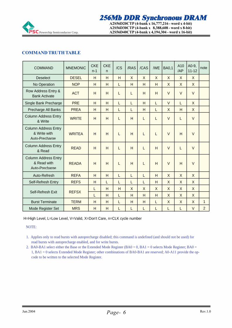
COMMAND TRUTH TABLE
H=High Level, L=Low Level, V=Valid, X=Don't Care, n=CLK cycle number
COMMAND MNEMONIC CKEn-1
CKEn
/CS /RAS /CAS /WE BA0,1 A10/AP
A0-9,11-12
Deselect DESEL H H H X X X X X X
No Operation NOP H H L H H H X X X
Row Address Entry &Bank Activate
ACT H H L L H H V V V
Single Bank Precharge PRE H H L L H L V L X
Precharge All Banks PREA H H L L H L H X
Column Address Entry& Write
WRITE H H L H L L V L V
Column Address Entry& Write with
Auto-PrechargeWRITEA H H L H L L V H V
Column Address Entry& Read
READ H H L H L H V L V
Column Address Entry& Read with
Auto-PrechargeREADA H H L H L H V H V
Auto-Refresh REFA H H L L L H X X X
Self-Refresh Entry REFS H L L L L H X X X
Self-Refresh Exit REFSXL H H X X X X X X
L H L H H H X X X
Burst Terminate TERM H H L H H L X X X
Mode Register Set MRS H H L L L L L L V
X
note
1
NOTE:
1. Applies only to read bursts with autoprecharge disabled; this command is undefined (and should not be used) for read bursts with autoprecharge enabled, and for write bursts.
2. BA0-BA1 select either the Base or the Extended Mode Register (BA0 = 0, BA1 = 0 selects Mode Register; BA0 = 1, BA1 = 0 selects Extended Mode Register; other combinations of BA0-BA1 are reserved; A0-A11 provide the op-code to be written to the selected Mode Register.
2
Jun.2004 Rev.1.0
256Mb DDR Synchronous DRAM256Mb DDR Synchronous DRAM256Mb DDR Synchronous DRAM256Mb DDR Synchronous DRAM256Mb DDR Synchronous DRAM
Powerchip Semiconductor Corp.
A2S56D20CTP (4-bank x 16,777,216 - word x 4-bit)A2S56D30CTP (4-bank x 8,388,608 - word x 8-bit)A2S56D40CTP (4-bank x 4,194,304 - word x 16-bit)
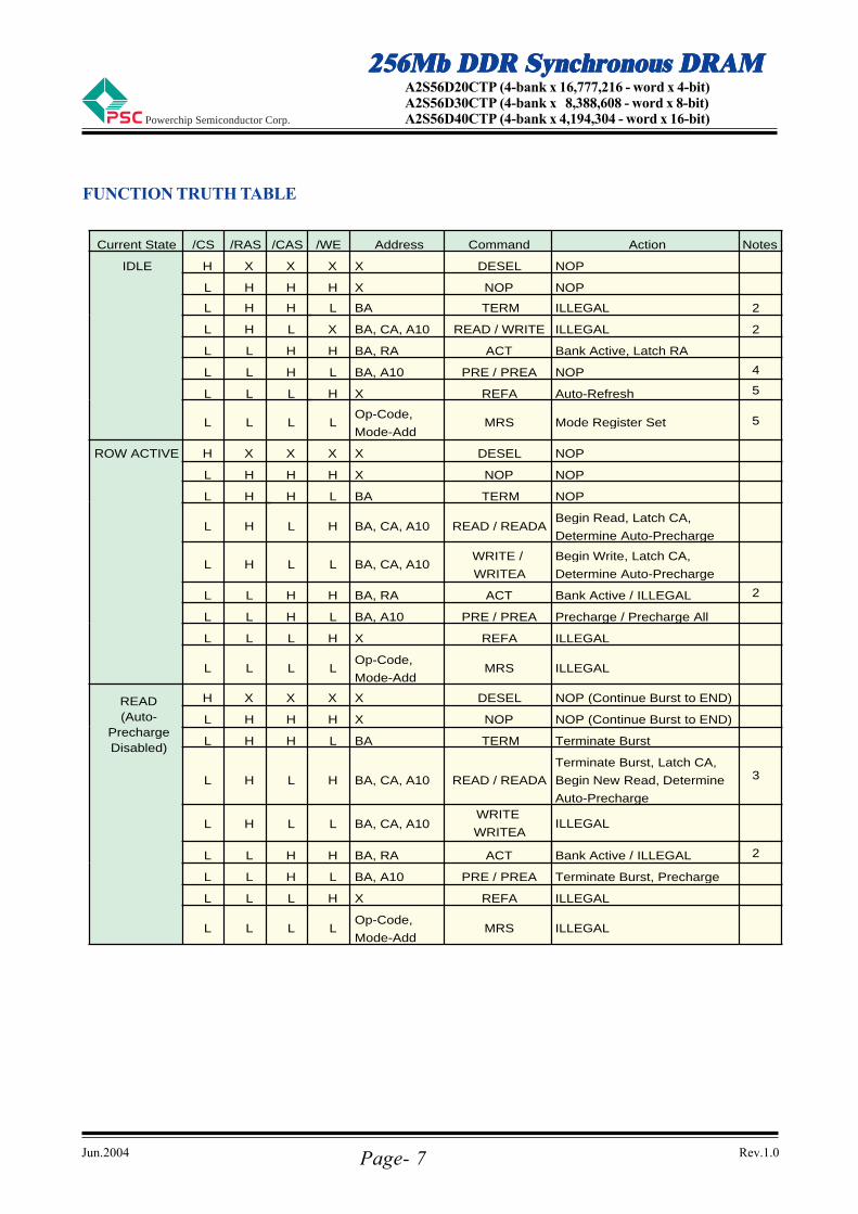
Current State /CS /RAS /CAS /WE Address Command Action
IDLE H X X X X DESEL NOP
L H H H X NOP NOP
L H H L BA TERM ILLEGAL
L H L X BA, CA, A10 READ / WRITE ILLEGAL
L L H H BA, RA ACT Bank Active, Latch RA
L L H L BA, A10 PRE / PREA NOP
L L L H X REFA Auto-Refresh
L L L LOp-Code,
Mode-AddMRS Mode Register Set
ROW ACTIVE H X X X X DESEL NOP
L H H H X NOP NOP
L H H L BA TERM NOP
L H L H BA, CA, A10 READ / READABegin Read, Latch CA,
Determine Auto-Precharge
L H L L BA, CA, A10WRITE /
WRITEA
Begin Write, Latch CA,
Determine Auto-Precharge
L L H H BA, RA ACT Bank Active / ILLEGAL
L L H L BA, A10 PRE / PREA Precharge / Precharge All
L L L H X REFA ILLEGAL
L L L LOp-Code,
Mode-AddMRS ILLEGAL
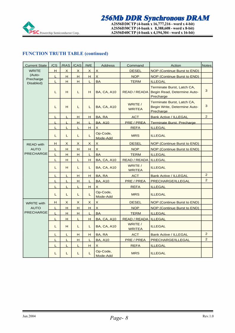
READ(Auto-
PrechargeDisabled)
H X X X X DESEL NOP (Continue Burst to END)
L H H H X NOP NOP (Continue Burst to END)
L H H L BA TERM Terminate Burst
L H L H BA, CA, A10 READ / READA
Terminate Burst, Latch CA,
Begin New Read, Determine
Auto-Precharge
L H L L BA, CA, A10WRITE
WRITEA
L L H H BA, RA ACT Bank Active / ILLEGAL
L L H L BA, A10 PRE / PREA Terminate Burst, Precharge
L L L H X REFA ILLEGAL
L L L LOp-Code,
Mode-AddMRS ILLEGAL
Notes
2
2
2
4
5
5
3
2
ILLEGAL
FUNCTION TRUTH TABLE
Page- 7
Jun.2004 Rev.1.0
256Mb DDR Synchronous DRAM256Mb DDR Synchronous DRAM256Mb DDR Synchronous DRAM256Mb DDR Synchronous DRAM256Mb DDR Synchronous DRAMA2S56D20CTP (4-bank x 16,777,216 - word x 4-bit)A2S56D30CTP (4-bank x 8,388,608 - word x 8-bit)A2S56D40CTP (4-bank x 4,194,304 - word x 16-bit)Powerchip Semiconductor Corp.
FUNCTION TRUTH TABLE (continued)
Current State /CS /RAS /CAS /WE Address Command Action
WRITE(Auto-
PrechargeDisabled)
H X X X X DESEL NOP (Continue Burst to END)
L H H H X NOP NOP (Continue Burst to END)
L H H L BA TERM ILLEGAL
L H L H BA, CA, A10 READ / READA
Terminate Burst, Latch CA,
Begin Read, Determine Auto-Precharge
L H L L BA, CA, A10WRITE /
WRITEA
Terminate Burst, Latch CA,
Begin Write, Determine Auto-Precharge
L L H H BA, RA ACT Bank Active / ILLEGAL
L L H L BA, A10 PRE / PREA Terminate Burst, Precharge
L L L H X REFA ILLEGAL
L L L LOp-Code,
Mode-AddMRS ILLEGAL
READ with
AUTO PRECHARGE
H X X X X DESEL NOP (Continue Burst to END)
L H H H X NOP NOP (Continue Burst to END)
L H H L BA TERM ILLEGAL
L H L H BA, CA, A10 READ / READA ILLEGAL
L H L L BA, CA, A10WRITE / WRITEA
ILLEGAL
L L H H BA, RA ACT Bank Active / ILLEGAL
L L H L BA, A10 PRE / PREA PRECHARGE/ILLEGAL
L L L H X REFA ILLEGAL
L L L LOp-Code, Mode-Add
MRS ILLEGAL
WRITE with
AUTO PRECHARGE
H X X X X DESEL NOP (Continue Burst to END)
L H H H X NOP NOP (Continue Burst to END)
L H H L BA TERM ILLEGAL
L H L H BA, CA, A10 READ / READA ILLEGAL
L H L L BA, CA, A10WRITE /
WRITEAILLEGAL
L L H H BA, RA ACT Bank Active / ILLEGAL
L L H L BA, A10 PRE / PREA PRECHARGE/ILLEGAL
L L L H X REFA ILLEGAL
L L L LOp-Code, Mode-Add
MRS ILLEGAL
Notes
3
3
2
2
2
2
2
Page- 8
Jun.2004 Rev.1.0
256Mb DDR Synchronous DRAM256Mb DDR Synchronous DRAM256Mb DDR Synchronous DRAM256Mb DDR Synchronous DRAM256Mb DDR Synchronous DRAM
Powerchip Semiconductor Corp.
A2S56D20CTP (4-bank x 16,777,216 - word x 4-bit)A2S56D30CTP (4-bank x 8,388,608 - word x 8-bit)A2S56D40CTP (4-bank x 4,194,304 - word x 16-bit)
Page- 9
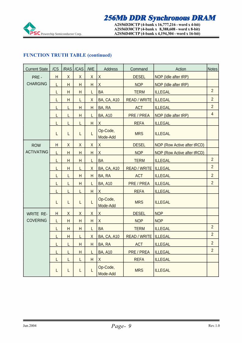
FUNCTION TRUTH TABLE (continued)
Current State /CS /RAS /CAS /WE Address Command Action
PRE -
CHARGING
H X X X X DESEL NOP (Idle after tRP)
L H H H X NOP NOP (Idle after tRP)
L H H L BA TERM ILLEGAL
L H L X BA, CA, A10 READ / WRITE ILLEGAL
L L H H BA, RA ACT ILLEGAL
L L H L BA, A10 PRE / PREA NOP (Idle after tRP)
L L L H X REFA ILLEGAL
L L L LOp-Code,
Mode-AddMRS ILLEGAL
ROW
ACTIVATING
H X X X X DESEL NOP (Row Active after tRCD)
L H H H X NOP NOP (Row Active after tRCD)
L H H L BA TERM ILLEGAL
L H L X BA, CA, A10 READ / WRITE ILLEGAL
L L H H BA, RA ACT ILLEGAL
L L H L BA, A10 PRE / PREA ILLEGAL
L L L H X REFA ILLEGAL
L L L LOp-Code,
Mode-AddMRS ILLEGAL
WRITE RE-
COVERING
H X X X X DESEL NOP
L H H H X NOP NOP
L H H L BA TERM ILLEGAL
L H L X BA, CA, A10 READ / WRITE ILLEGAL
L L H H BA, RA ACT ILLEGAL
L L H L BA, A10 PRE / PREA ILLEGAL
L L L H X REFA ILLEGAL
L L L LOp-Code,
Mode-AddMRS ILLEGAL
Notes
2
2
2
4
2
2
2
2
2
2
2
2
Jun.2004 Rev.1.0
256Mb DDR Synchronous DRAM256Mb DDR Synchronous DRAM256Mb DDR Synchronous DRAM256Mb DDR Synchronous DRAM256Mb DDR Synchronous DRAMA2S56D20CTP (4-bank x 16,777,216 - word x 4-bit)A2S56D30CTP (4-bank x 8,388,608 - word x 8-bit)A2S56D40CTP (4-bank x 4,194,304 - word x 16-bit)Powerchip Semiconductor Corp.
Page- 10
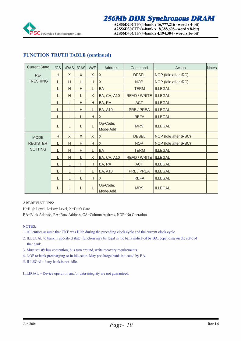
FUNCTION TRUTH TABLE (continued)
Current State /CS /RAS /CAS /WE Address Command Action
RE-
FRESHING
H X X X X DESEL NOP (Idle after tRC)
L H H H X NOP NOP (Idle after tRC)
L H H L BA TERM ILLEGAL
L H L X BA, CA, A10 READ / WRITE ILLEGAL
L L H H BA, RA ACT ILLEGAL
L L H L BA, A10 PRE / PREA ILLEGAL
L L L H X REFA ILLEGAL
L L L LOp-Code,
Mode-AddMRS ILLEGAL
MODE
REGISTER
SETTING
H X X X X DESEL NOP (Idle after tRSC)
L H H H X NOP NOP (Idle after tRSC)
L H H L BA TERM ILLEGAL
L H L X BA, CA, A10 READ / WRITE ILLEGAL
L L H H BA, RA ACT ILLEGAL
L L H L BA, A10 PRE / PREA ILLEGAL
L L L H X REFA ILLEGAL
L L L LOp-Code,
Mode-AddMRS ILLEGAL
ABBREVIATIONS:
H=High Level, L=Low Level, X=Don't Care
BA=Bank Address, RA=Row Address, CA=Column Address, NOP=No Operation
NOTES:
1. All entries assume that CKE was High during the preceding clock cycle and the current clock cycle.
2. ILLEGAL to bank in specified state; function may be legal in the bank indicated by BA, depending on the state of
that bank.
3. Must satisfy bus contention, bus turn around, write recovery requirements.
4. NOP to bank precharging or in idle state. May precharge bank indicated by BA.
5. ILLEGAL if any bank is not idle.
ILLEGAL = Device operation and/or data-integrity are not guaranteed.
Notes
Jun.2004 Rev.1.0
256Mb DDR Synchronous DRAM256Mb DDR Synchronous DRAM256Mb DDR Synchronous DRAM256Mb DDR Synchronous DRAM256Mb DDR Synchronous DRAM
Powerchip Semiconductor Corp.
A2S56D20CTP (4-bank x 16,777,216 - word x 4-bit)A2S56D30CTP (4-bank x 8,388,608 - word x 8-bit)A2S56D40CTP (4-bank x 4,194,304 - word x 16-bit)
Page- 11
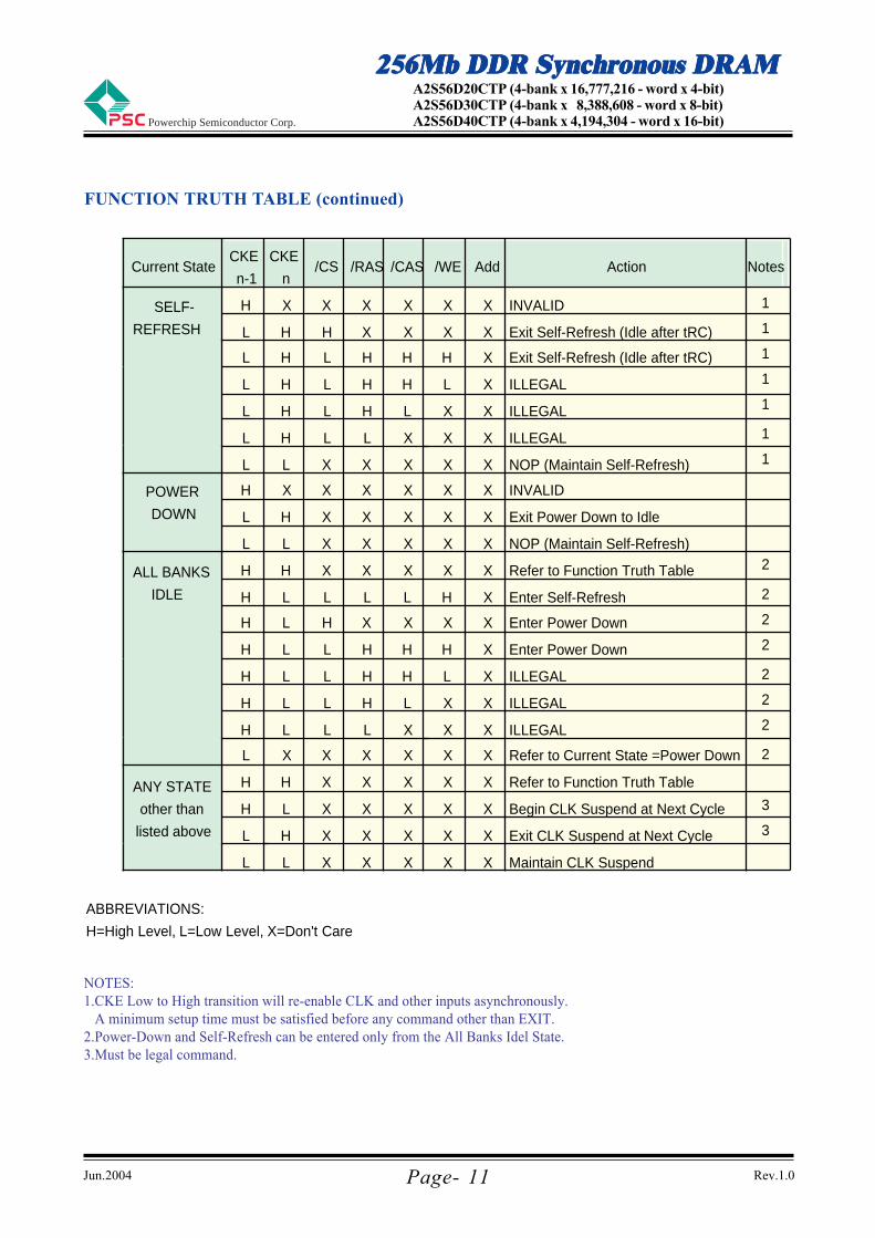
FUNCTION TRUTH TABLE (continued)
Current StateCKE
n-1
CKE
n/CS /RAS /CAS /WE Add Action
SELF-
REFRESH
H X X X X X X INVALID
L H H X X X X Exit Self-Refresh (Idle after tRC)
L H L H H H X Exit Self-Refresh (Idle after tRC)
L H L H H L X ILLEGAL
L H L H L X X ILLEGAL
L H L L X X X ILLEGAL
L L X X X X X NOP (Maintain Self-Refresh)
POWER
DOWN
H X X X X X X INVALID
L H X X X X X Exit Power Down to Idle
L L X X X X X NOP (Maintain Self-Refresh)
ALL BANKS
IDLE
H H X X X X X Refer to Function Truth Table
H L L L L H X Enter Self-Refresh
H L H X X X X Enter Power Down
H L L H H H X Enter Power Down
H L L H H L X ILLEGAL
H L L H L X X ILLEGAL
H L L L X X X ILLEGAL
L X X X X X X Refer to Current State =Power Down
ANY STATE
other than
listed above
H H X X X X X Refer to Function Truth Table
H L X X X X X Begin CLK Suspend at Next Cycle
L H X X X X X Exit CLK Suspend at Next Cycle
L L X X X X X Maintain CLK Suspend
ABBREVIATIONS:
H=High Level, L=Low Level, X=Don't Care
Notes
3
3
2
2
2
2
2
2
2
2
1
1
1
1
1
1
1
NOTES:1.CKE Low to High transition will re-enable CLK and other inputs asynchronously. A minimum setup time must be satisfied before any command other than EXIT.2.Power-Down and Self-Refresh can be entered only from the All Banks Idel State.3.Must be legal command.
Jun.2004 Rev.1.0
256Mb DDR Synchronous DRAM256Mb DDR Synchronous DRAM256Mb DDR Synchronous DRAM256Mb DDR Synchronous DRAM256Mb DDR Synchronous DRAMA2S56D20CTP (4-bank x 16,777,216 - word x 4-bit)A2S56D30CTP (4-bank x 8,388,608 - word x 8-bit)A2S56D40CTP (4-bank x 4,194,304 - word x 16-bit)Powerchip Semiconductor Corp.
Page- 12
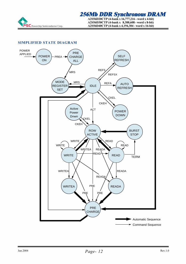
SIMPLIFIED STATE DIAGRAM
ROWACTIVE
IDLE
PRECHARGE
POWERDOWN
READAWRITEA
POWERON
ACT
REFA
REFS
REFSX
CKEL
CKEH
MRS
CKEL
CKEH
WRITE READ
WRITEA
WRITEA READA
READ
PRE
READA
READA
PRE PRE
PREA
POWERAPPLIED
MODEREGISTER
SET
SELFREFRESH
AUTOREFRESH
ActivePowerDown
Automatic Sequence
Command Sequence
WRITE READ
PRECHARGE
ALL
MRS
BURSTSTOP
TERMREADWRITE
Jun.2004 Rev.1.0
256Mb DDR Synchronous DRAM256Mb DDR Synchronous DRAM256Mb DDR Synchronous DRAM256Mb DDR Synchronous DRAM256Mb DDR Synchronous DRAM
Powerchip Semiconductor Corp.
A2S56D20CTP (4-bank x 16,777,216 - word x 4-bit)A2S56D30CTP (4-bank x 8,388,608 - word x 8-bit)A2S56D40CTP (4-bank x 4,194,304 - word x 16-bit)
R: Reserved for Future Use
BL
0 0 00 0 10 1 00 1 11 0 01 0 11 1 01 1 1
BurstLength
BT= 0 BT= 1
R248RRRR
R248RRRR
01
BurstType
SequentialInterleaved
A11 A10 A9 A8 A7 A6 A5 A4 A3 A2 A1 A0BA1 BA0
0 0 DR 0 LTMODE BT BL00 0
/CS
/RAS
/CAS
/WE
A11-A0
/CLK
V
CLK
BA0
BA1
CL
LatencyMode
/CAS Latency
RR23R
1.52.5R
0 0 0 0 0 1 0 1 00 1 11 0 01 0 11 1 01 1 1
01
DLLReset
NOYES
A12
0
Page- 13
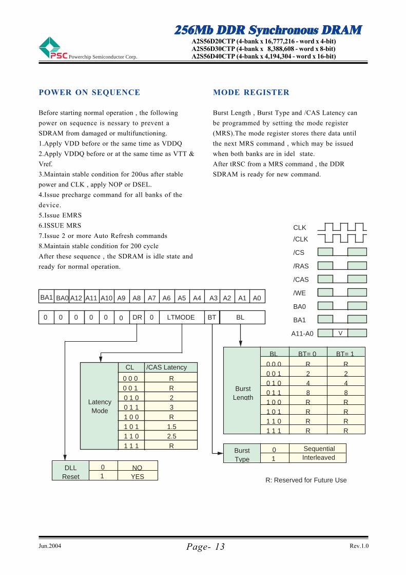
POWER ON SEQUENCE MODE REGISTER
Before starting normal operation , the following
power on sequence is nessary to prevent a
SDRAM from damaged or multifunctioning.
1.Apply VDD before or the same time as VDDQ
2.Apply VDDQ before or at the same time as VTT &
Vref.
3.Maintain stable condition for 200us after stable
power and CLK , apply NOP or DSEL.
4.Issue precharge command for all banks of the
device.
5.Issue EMRS
6.ISSUE MRS
7.Issue 2 or more Auto Refresh commands
8.Maintain stable condition for 200 cycle
After these sequence , the SDRAM is idle state and
ready for normal operation.
Burst Length , Burst Type and /CAS Latency can
be programmed by setting the mode register
(MRS).The mode register stores there data until
the next MRS command , which may be issued
when both banks are in idel state.
After tRSC from a MRS command , the DDR
SDRAM is ready for new command.
Jun.2004 Rev.1.0
256Mb DDR Synchronous DRAM256Mb DDR Synchronous DRAM256Mb DDR Synchronous DRAM256Mb DDR Synchronous DRAM256Mb DDR Synchronous DRAMA2S56D20CTP (4-bank x 16,777,216 - word x 4-bit)A2S56D30CTP (4-bank x 8,388,608 - word x 8-bit)A2S56D40CTP (4-bank x 4,194,304 - word x 16-bit)Powerchip Semiconductor Corp.
/CS
/RAS
/CAS
/WE
A11-A0
/CLK
V
CLK
BA0
BA1
01
DLLDisable
DLL enableDLL disable
A11 A10 A9 A8 A7 A6 A5 A4 A3 A2 A1 A0BA1 BA0
0 0 0 0 DD10 0 DS0 0 0 0
01
DriveStrength
NormalWeak
A12
0 0
Page- 14
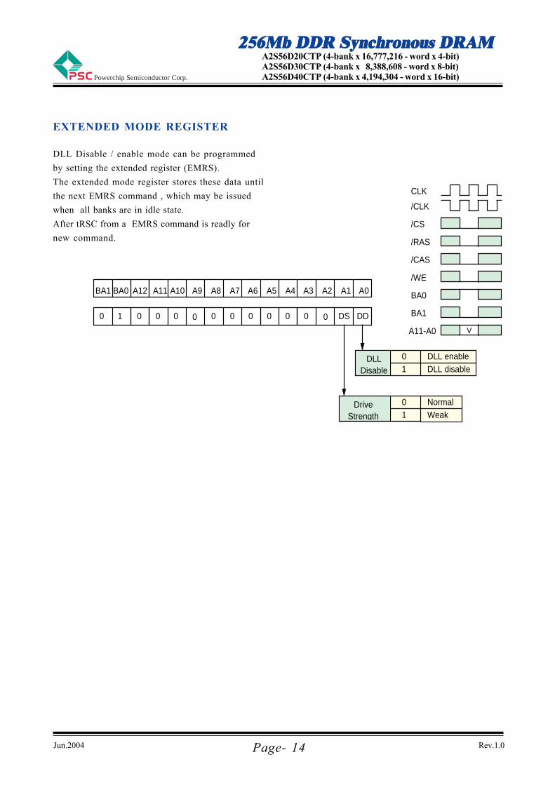
EXTENDED MODE REGISTER
DLL Disable / enable mode can be programmed
by setting the extended register (EMRS).
The extended mode register stores these data until
the next EMRS command , which may be issued
when all banks are in idle state.
After tRSC from a EMRS command is readly for
new command.
Jun.2004 Rev.1.0
256Mb DDR Synchronous DRAM256Mb DDR Synchronous DRAM256Mb DDR Synchronous DRAM256Mb DDR Synchronous DRAM256Mb DDR Synchronous DRAM
Powerchip Semiconductor Corp.
A2S56D20CTP (4-bank x 16,777,216 - word x 4-bit)A2S56D30CTP (4-bank x 8,388,608 - word x 8-bit)A2S56D40CTP (4-bank x 4,194,304 - word x 16-bit)
Page- 15
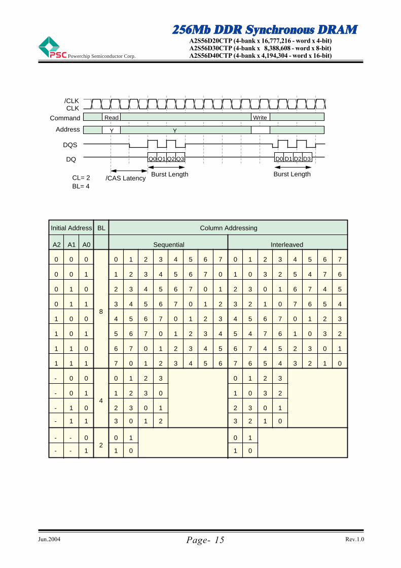
/CAS LatencyBurst LengthCL= 2
BL= 4
Burst Length
A2 A1 A0
Initial Address BL
Sequential Interleaved
Column Addressing
0 0 0
0 0 1
0 1 0
0 1 1
1 0 0
1 0 1
1 1 0
1 1 1
- 0 0
- 0 1
- 1 0
- 1 1
- - 0
0 1 2 3 4 5 6 7 0 1 2 3 4 5 6 7
1 2 3 4 5 6 7 0 1 0 3 2 5 4 7 6
2 3 4 5 6 7 0 1 2 3 0 1 6 7 4 5
3 4 5 6 7 0 1 2 3 2 1 0 7 6 5 4
4 5 6 7 0 1 2 3 4 5 6 7 0 1 2 3
5 6 7 0 1 2 3 4 5 4 7 6 1 0 3 2
6 7 0 1 2 3 4 5 6 7 4 5 2 3 0 1
7 0 1 2
0 1 2 3
1 2 3 0
2 3 0 1
3 0
0 1
7 6 5 4
0 1 2 3
1 0 3 2
2 3 0 1
3 2
0 1
- - 1
1 2
1 0
3 4 5 6 3 2 1 0
1 0
1 0
8
4
2
Command
Address
DQ
Y Y
Read Write
DQS
Q0 Q1 Q2 Q3 D0 D1 D2 D3
/CLKCLK
Jun.2004 Rev.1.0
256Mb DDR Synchronous DRAM256Mb DDR Synchronous DRAM256Mb DDR Synchronous DRAM256Mb DDR Synchronous DRAM256Mb DDR Synchronous DRAMA2S56D20CTP (4-bank x 16,777,216 - word x 4-bit)A2S56D30CTP (4-bank x 8,388,608 - word x 8-bit)A2S56D40CTP (4-bank x 4,194,304 - word x 16-bit)Powerchip Semiconductor Corp.
Page- 16
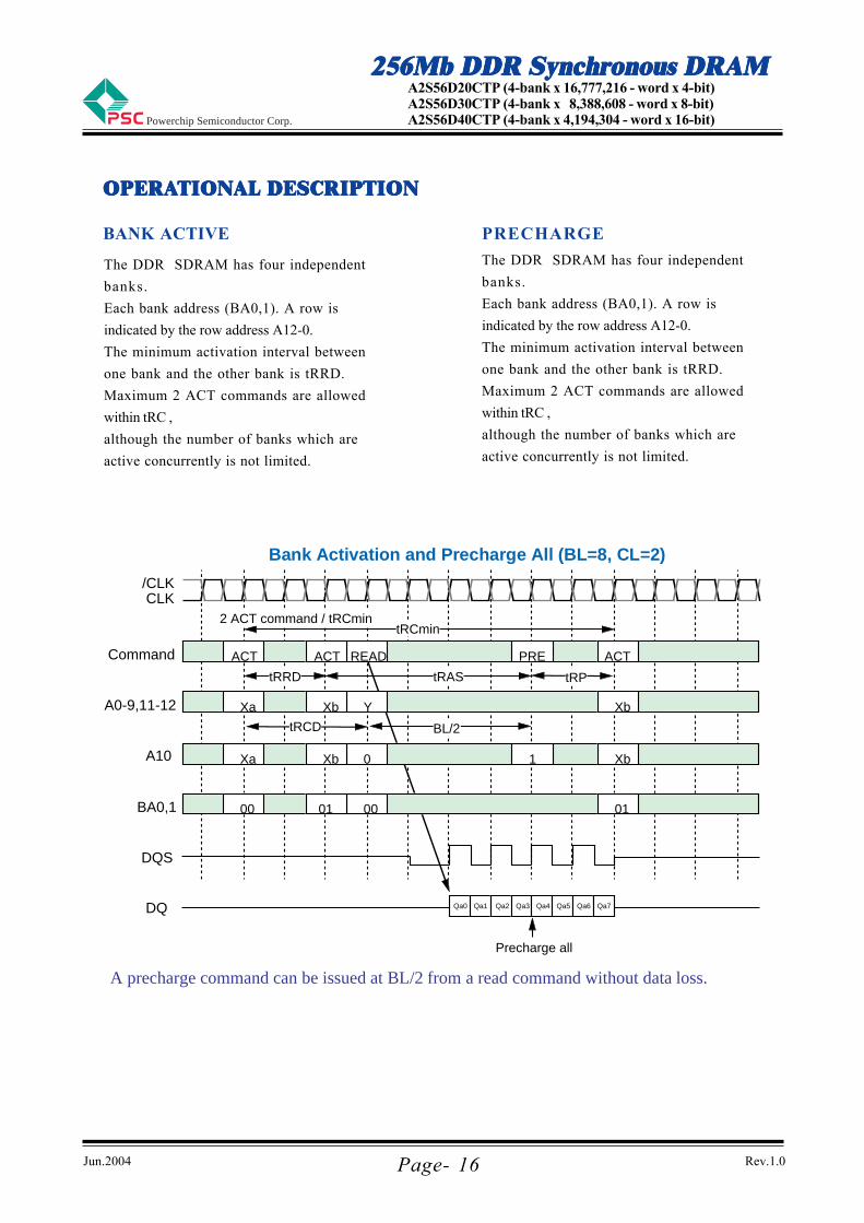
OPERAOPERAOPERAOPERAOPERATIONTIONTIONTIONTIONAL DESCRIPTIONAL DESCRIPTIONAL DESCRIPTIONAL DESCRIPTIONAL DESCRIPTION
The DDR SDRAM has four independent
banks.
Each bank address (BA0,1). A row is
indicated by the row address A12-0.
The minimum activation interval between
one bank and the other bank is tRRD.
Maximum 2 ACT commands are allowed
within tRC ,
although the number of banks which are
active concurrently is not limited.
BANK ACTIVE PRECHARGE
The DDR SDRAM has four independent
banks.
Each bank address (BA0,1). A row is
indicated by the row address A12-0.
The minimum activation interval between
one bank and the other bank is tRRD.
Maximum 2 ACT commands are allowed
within tRC ,
although the number of banks which are
active concurrently is not limited.
A precharge command can be issued at BL/2 from a read command without data loss.
Precharge all
Bank Activation and Precharge All (BL=8, CL=2)
Command
A0-9,11-12
A10
BA0,1
DQ
ACT
Xa
Xa
00
READ
Y
0
00
ACT
Xb
Xb
01
PRE
tRRD
tRCD
1
ACT
Xb
Xb
01
tRAS tRP
tRCmin2 ACT command / tRCmin
DQS
Qa0
BL/2
Qa1 Qa2 Qa3 Qa4 Qa5 Qa6 Qa7
/CLKCLK
Jun.2004 Rev.1.0
256Mb DDR Synchronous DRAM256Mb DDR Synchronous DRAM256Mb DDR Synchronous DRAM256Mb DDR Synchronous DRAM256Mb DDR Synchronous DRAM
Powerchip Semiconductor Corp.
A2S56D20CTP (4-bank x 16,777,216 - word x 4-bit)A2S56D30CTP (4-bank x 8,388,608 - word x 8-bit)A2S56D40CTP (4-bank x 4,194,304 - word x 16-bit)
Page-1 7
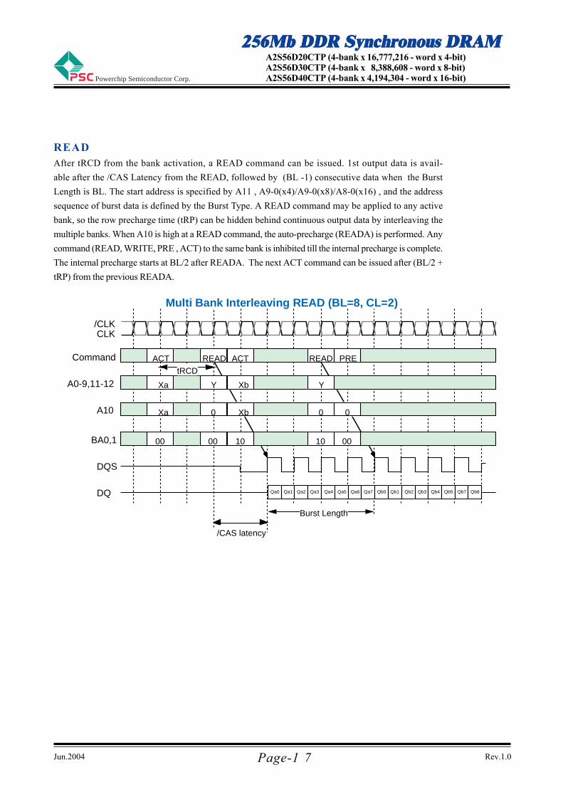
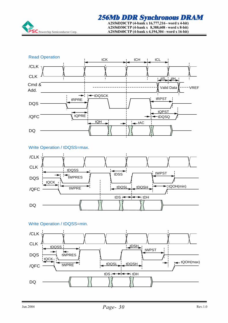
READAfter tRCD from the bank activation, a READ command can be issued. 1st output data is avail-
able after the /CAS Latency from the READ, followed by (BL -1) consecutive data when the Burst
Length is BL. The start address is specified by A11 , A9-0(x4)/A9-0(x8)/A8-0(x16) , and the address
sequence of burst data is defined by the Burst Type. A READ command may be applied to any active
bank, so the row precharge time (tRP) can be hidden behind continuous output data by interleaving the
multiple banks. When A10 is high at a READ command, the auto-precharge (READA) is performed. Any
command (READ, WRITE, PRE , ACT) to the same bank is inhibited till the internal precharge is complete.
The internal precharge starts at BL/2 after READA. The next ACT command can be issued after (BL/2 +
tRP) from the previous READA.
Multi Bank Interleaving READ (BL=8, CL=2)
/CLK
Command
A0-9,11-12
A10
BA0,1
DQ
ACT
Xa
Xa
00
READ
Y
0
00
READ
Y
0
10
ACT
Xb
Xb
10
PRE
0
00
tRCD
/CAS latency
Burst Length
DQS
Qa0
CLK
Qa1 Qa2 Qa3 Qa4 Qa5 Qa6 Qa7 Qb0 Qb1 Qb2 Qb3 Qb4 Qb5 Qb7 Qb8
Jun.2004 Rev.1.0
256Mb DDR Synchronous DRAM256Mb DDR Synchronous DRAM256Mb DDR Synchronous DRAM256Mb DDR Synchronous DRAM256Mb DDR Synchronous DRAMA2S56D20CTP (4-bank x 16,777,216 - word x 4-bit)A2S56D30CTP (4-bank x 8,388,608 - word x 8-bit)A2S56D40CTP (4-bank x 4,194,304 - word x 16-bit)Powerchip Semiconductor Corp.
Page-1 8
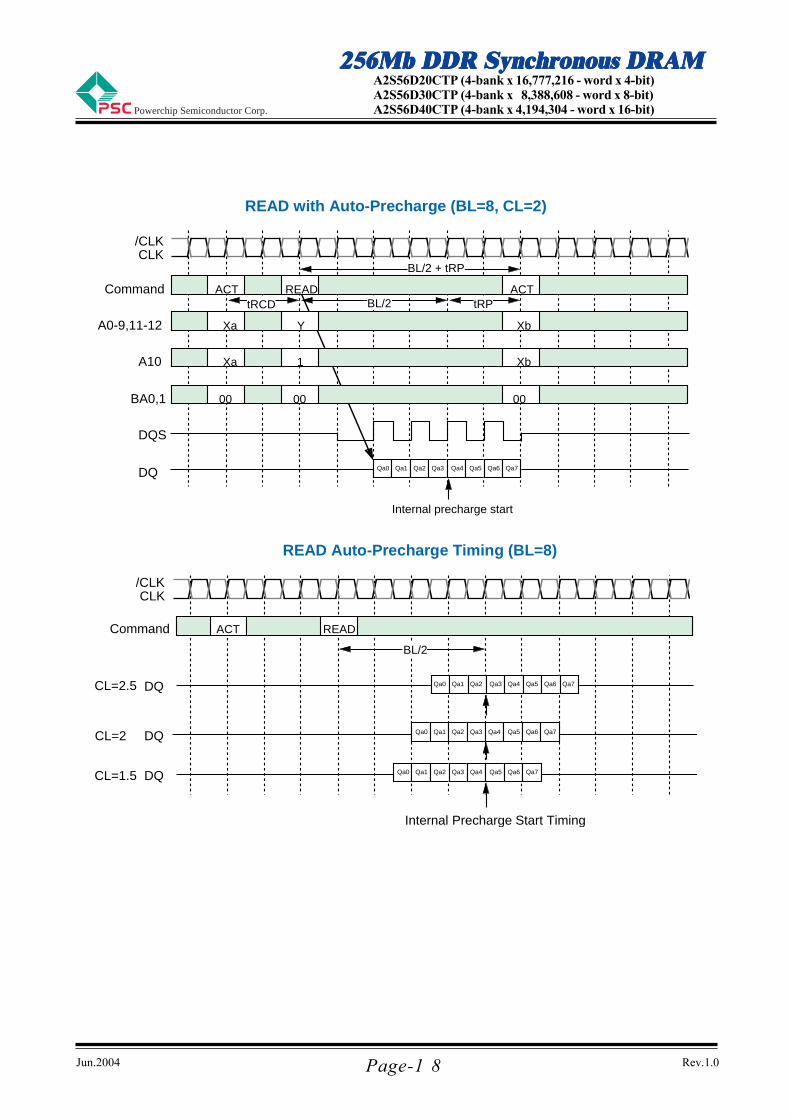
READ with Auto-Precharge (BL=8, CL=2)
Command
A0-9,11-12
A10
BA0,1
DQ
ACT
Xa
Xa
00
READ
Y
1
00
ACT
Xb
Xb
00
Internal precharge start
tRCD tRP
BL/2 + tRP
BL/2
DQS
/CLKCLK
READ Auto-Precharge Timing (BL=8)
Command ACT READ
Internal Precharge Start Timing
DQ
DQ
CL=2.5
CL=1.5
BL/2
Qa0
DQCL=2 Qa0
/CLKCLK
Qa0 Qa1 Qa2 Qa3 Qa4 Qa5 Qa6 Qa7
Qa0 Qa1 Qa2 Qa3 Qa4 Qa5 Qa6 Qa7
Qa1 Qa2 Qa3 Qa4 Qa5 Qa6 Qa7
Qa1 Qa2 Qa3 Qa4 Qa5 Qa6 Qa7
Jun.2004 Rev.1.0
256Mb DDR Synchronous DRAM256Mb DDR Synchronous DRAM256Mb DDR Synchronous DRAM256Mb DDR Synchronous DRAM256Mb DDR Synchronous DRAM
Powerchip Semiconductor Corp.
A2S56D20CTP (4-bank x 16,777,216 - word x 4-bit)A2S56D30CTP (4-bank x 8,388,608 - word x 8-bit)A2S56D40CTP (4-bank x 4,194,304 - word x 16-bit)
Page- 19
WRITEAfter tRCD from the bank activation , a WRITE command can be issued. 1st input data is set at the same
cycle as the WRITE. Following (BL -1) data are written into the RAM, when the Burst Length is BL. The start
address is specified by A11 , A9-0(x4)/A9-0(x8)/A8-0(x16) and the address sequence of burst data is defined by the
Burst Type. A WRITE command may be applied to any active bank, so the row precharge time (tRP) can be hidden
behind continuous input data by interleaving the multiple banks. From the last input data to the PRE command, the write
recovery time (tWR) is required. When A10 is high at a WRITE command, the autoprecharge (WRITEA) is performed.
Any command (READ, WRITE, PRE, TBST, ACT) to the same bank is inhibited till the internal precharge is complete.
The internal precharge begins at tWR after the last input data cycle. (Need to keep tRAS min.) The next ACT command
can be issued after tRP from the internal precharge timing.
Multi Bank Interleaving WRITE (BL=8)
Command
A0-9,11-12
A10
BA0,1
DQ
ACT
Xa
00
WRITE
00
WRITE
0 0
10
ACT
Xb
10
0
10
tRCD tRCDPRE
Xa 0
00
PRE
DQS
WRITE with Auto-Precharge (BL=8)
Command
A0-9,11-12
A10
BA0,1
DQ
ACT
Xa
00
WRITE
1
00
ACT
Xb
00
tRCD
Da0
DQS
/CLKCLK
/CLKCLK
Da1 Da2 Da3 Da4 Da5 Da6 Da7
Da0 Da1 Da2 Da3 Da4 Da5 Da6 Da7 Db0 Db1 Db2 Db3
tDAL
Db4 Db5 Db6 Db7
Xa Y Xb
Xa Ya YbXb
Jun.2004 Rev.1.0
256Mb DDR Synchronous DRAM256Mb DDR Synchronous DRAM256Mb DDR Synchronous DRAM256Mb DDR Synchronous DRAM256Mb DDR Synchronous DRAMA2S56D20CTP (4-bank x 16,777,216 - word x 4-bit)A2S56D30CTP (4-bank x 8,388,608 - word x 8-bit)A2S56D40CTP (4-bank x 4,194,304 - word x 16-bit)Powerchip Semiconductor Corp.
Read Interrupted by Precharge (BL=8)
CL=2.5
Command
DQS
Command
DQ
Command
DQ
Q0 Q1 Q2 Q3
Q0 Q1
Read Interrupted by Read (BL=8, CL=2)
Command
A0-9,11
A10
BA0,1
DQ
Yi
READ READ READ READ
Yj Yk Yl
0 00 0
00 1000 01
DQS
Qai0 Qai1 Qaj0 Qaj1 Qaj2 Qaj3 Qak0 Qak1 Qak2 Qak3 Qak4 Qak5 Qal0 Qal1 Qal2 Qal3 Qal4 Qal5 Qal6 Qal7
/CLKCLK
/CLKCLK
DQ Q0 Q1 Q2 Q3 Q4 Q5
PREREAD
READ PRE
READ PRE
DQS
DQS
Page- 2 0
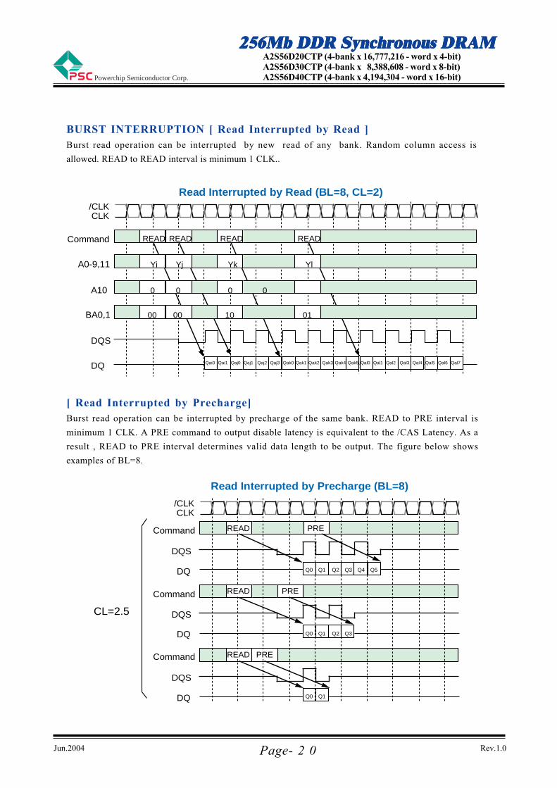
BURST INTERRUPTION [ Read Interrupted by Read ]Burst read operation can be interrupted by new read of any bank. Random column access is
allowed. READ to READ interval is minimum 1 CLK..
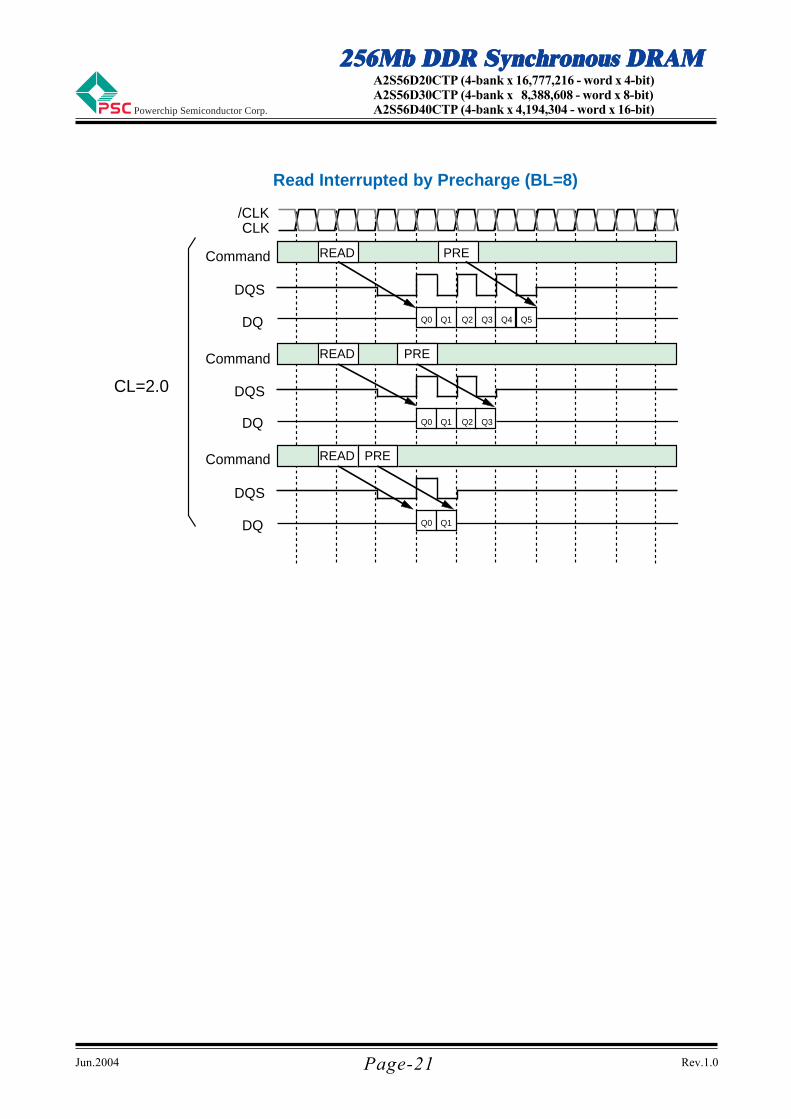
[ Read Interrupted by Precharge]Burst read operation can be interrupted by precharge of the same bank. READ to PRE interval is
minimum 1 CLK. A PRE command to output disable latency is equivalent to the /CAS Latency. As a
result , READ to PRE interval determines valid data length to be output. The figure below shows
examples of BL=8.
Jun.2004 Rev.1.0
256Mb DDR Synchronous DRAM256Mb DDR Synchronous DRAM256Mb DDR Synchronous DRAM256Mb DDR Synchronous DRAM256Mb DDR Synchronous DRAM
Powerchip Semiconductor Corp.
A2S56D20CTP (4-bank x 16,777,216 - word x 4-bit)A2S56D30CTP (4-bank x 8,388,608 - word x 8-bit)A2S56D40CTP (4-bank x 4,194,304 - word x 16-bit)
Page-21
Read Interrupted by Precharge (BL=8)
CL=2.0
/CLKCLK
Command
DQS
Command
DQ
Command
DQ
Q0 Q1 Q2 Q3
Q0 Q1
DQ Q0 Q1 Q2 Q3 Q4 Q5
PREREAD
READ PRE
READ PRE
DQS
DQS
Jun.2004 Rev.1.0
256Mb DDR Synchronous DRAM256Mb DDR Synchronous DRAM256Mb DDR Synchronous DRAM256Mb DDR Synchronous DRAM256Mb DDR Synchronous DRAMA2S56D20CTP (4-bank x 16,777,216 - word x 4-bit)A2S56D30CTP (4-bank x 8,388,608 - word x 8-bit)A2S56D40CTP (4-bank x 4,194,304 - word x 16-bit)Powerchip Semiconductor Corp.
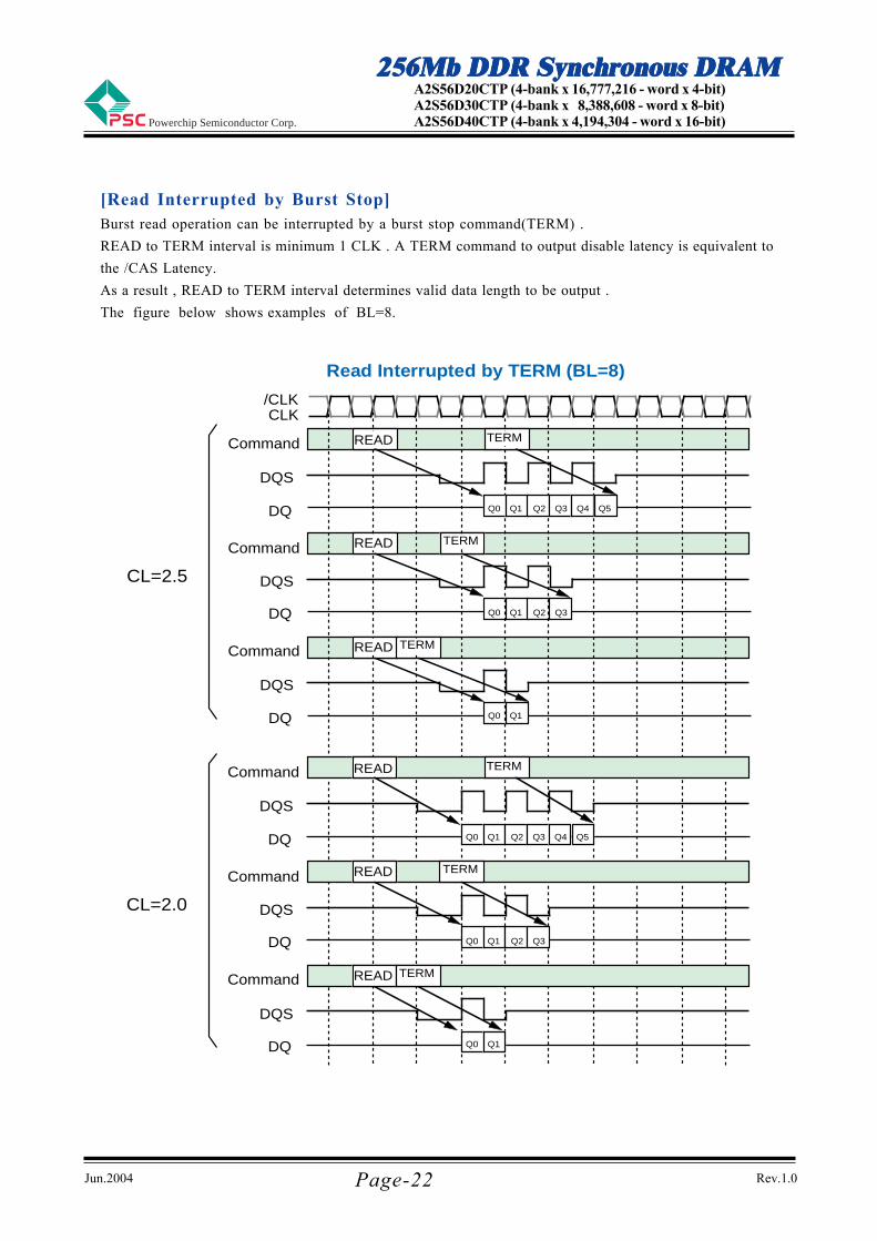
[Read Interrupted by Burst Stop]Burst read operation can be interrupted by a burst stop command(TERM) .
READ to TERM interval is minimum 1 CLK . A TERM command to output disable latency is equivalent to
the /CAS Latency.
As a result , READ to TERM interval determines valid data length to be output .
The figure below shows examples of BL=8.
Read Interrupted by TERM (BL=8)
CL=2.5
Command
DQS
Command
DQ
Command
DQ
Q0 Q1 Q2 Q3
Q0 Q1
/CLKCLK
DQ Q0 Q1 Q2 Q3 Q4 Q5
TERMREAD
READ TERM
READ TERM
DQS
DQS
CL=2.0
Command
DQS
Command
DQ
Command
DQ
Q0 Q1 Q2 Q3
Q0 Q1
DQ Q0 Q1 Q2 Q3 Q4 Q5
TERMREAD
READ TERM
READ TERM
DQS
DQS
Page-22
Jun.2004 Rev.1.0
256Mb DDR Synchronous DRAM256Mb DDR Synchronous DRAM256Mb DDR Synchronous DRAM256Mb DDR Synchronous DRAM256Mb DDR Synchronous DRAM
Powerchip Semiconductor Corp.
A2S56D20CTP (4-bank x 16,777,216 - word x 4-bit)A2S56D30CTP (4-bank x 8,388,608 - word x 8-bit)A2S56D40CTP (4-bank x 4,194,304 - word x 16-bit)
Page- 23
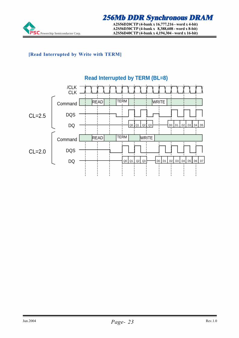
[Read Interrupted by Write with TERM]
Read Interrupted by TERM (BL=8)
CL=2.5
Command
DQ Q0 Q1 Q2 Q3
/CLKCLK
READ TERM
DQS
WRITE
D0 D1 D2 D3 D4 D5
CL=2.0
Command
DQ Q0 Q1 Q2 Q3
READ TERM
DQS
WRITE
D0 D1 D2 D3 D4 D5 D6 D7
Jun.2004 Rev.1.0
256Mb DDR Synchronous DRAM256Mb DDR Synchronous DRAM256Mb DDR Synchronous DRAM256Mb DDR Synchronous DRAM256Mb DDR Synchronous DRAMA2S56D20CTP (4-bank x 16,777,216 - word x 4-bit)A2S56D30CTP (4-bank x 8,388,608 - word x 8-bit)A2S56D40CTP (4-bank x 4,194,304 - word x 16-bit)Powerchip Semiconductor Corp.
Write Interrupted by Write (BL=8)
Command
A0-9,11
A10
BA0,1
WRITE
Yi
0
00
WRITE
Yk
0
10
WRITE
Yj
0
00
WRITE
Yl
0
00
DQ Dai1 Daj1 Daj3 Dak1 Dak3 Dak5 Dal1
DQS
Dal2 Dal3 Dal5 Dal6 Dal7Dal4Dal0Dak4Dak2Dak0Dai0 Daj0 Daj2
/CLKCLK
Write Interrupted by Read (BL=8, CL=2.5)
Command
A0-9,11-12
A10
BA0,1
DQ
WRITE
Yi
0
00
READ
Yj
0
00
Dai0 Dai1 Qaj0 Qaj1 Qaj2 Qaj3
QS
Qaj4 Qaj5 Qaj6 Qaj7
DMtWTR
/CLKCLK
Page- 24
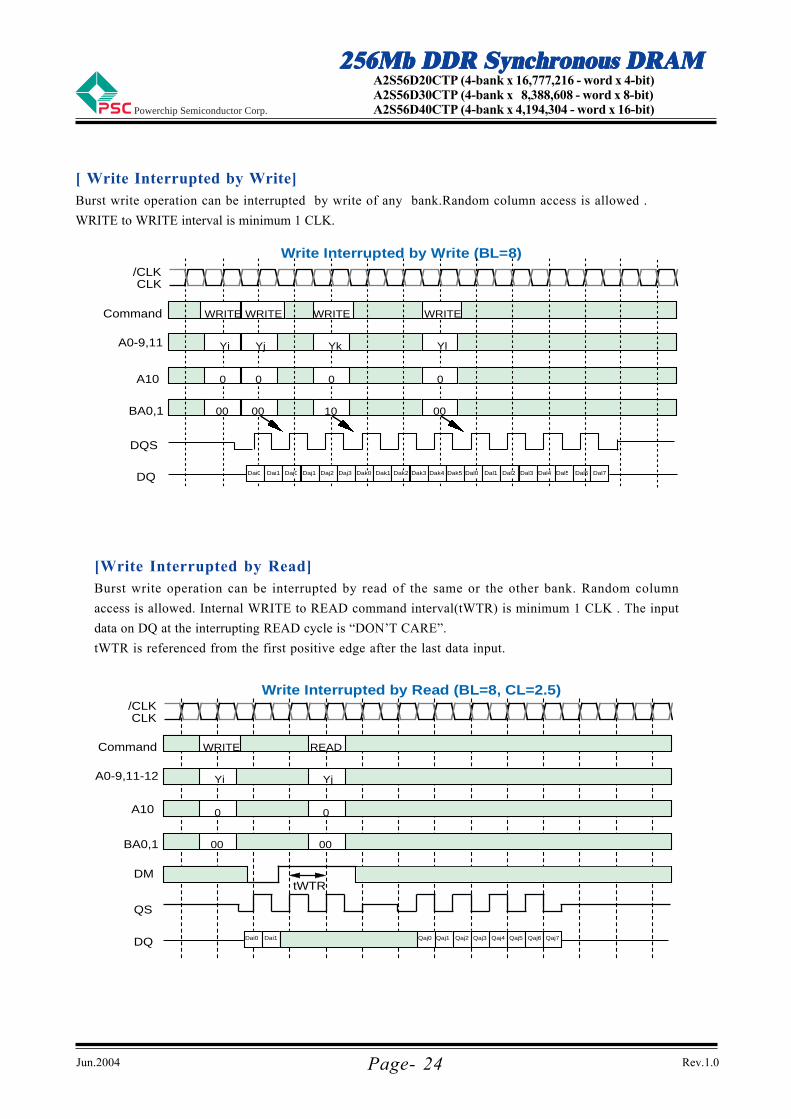
[ Write Interrupted by Write]Burst write operation can be interrupted by write of any bank.Random column access is allowed .
WRITE to WRITE interval is minimum 1 CLK.
[Write Interrupted by Read]Burst write operation can be interrupted by read of the same or the other bank. Random column
access is allowed. Internal WRITE to READ command interval(tWTR) is minimum 1 CLK . The input
data on DQ at the interrupting READ cycle is “DON’T CARE”.
tWTR is referenced from the first positive edge after the last data input.
Jun.2004 Rev.1.0
256Mb DDR Synchronous DRAM256Mb DDR Synchronous DRAM256Mb DDR Synchronous DRAM256Mb DDR Synchronous DRAM256Mb DDR Synchronous DRAM
Powerchip Semiconductor Corp.
A2S56D20CTP (4-bank x 16,777,216 - word x 4-bit)A2S56D30CTP (4-bank x 8,388,608 - word x 8-bit)A2S56D40CTP (4-bank x 4,194,304 - word x 16-bit)
Page- 25
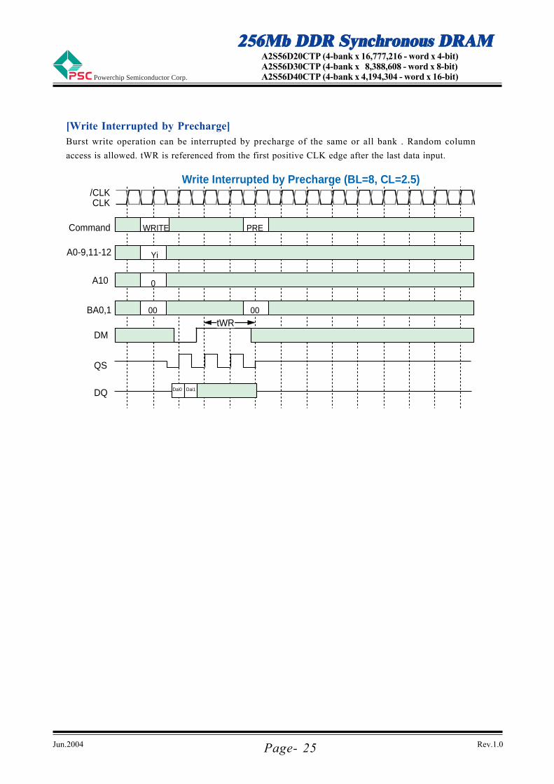
[Write Interrupted by Precharge]Burst write operation can be interrupted by precharge of the same or all bank . Random column
access is allowed. tWR is referenced from the first positive CLK edge after the last data input.
Write Interrupted by Precharge (BL=8, CL=2.5)
Command
A0-9,11-12
A10
BA0,1
DQ
WRITE
Yi
0
00
PRE
00
Dai0 Dai1
QS
DMtWR
/CLKCLK
Jun.2004 Rev.1.0
256Mb DDR Synchronous DRAM256Mb DDR Synchronous DRAM256Mb DDR Synchronous DRAM256Mb DDR Synchronous DRAM256Mb DDR Synchronous DRAMA2S56D20CTP (4-bank x 16,777,216 - word x 4-bit)A2S56D30CTP (4-bank x 8,388,608 - word x 8-bit)A2S56D40CTP (4-bank x 4,194,304 - word x 16-bit)Powerchip Semiconductor Corp.
Page- 26
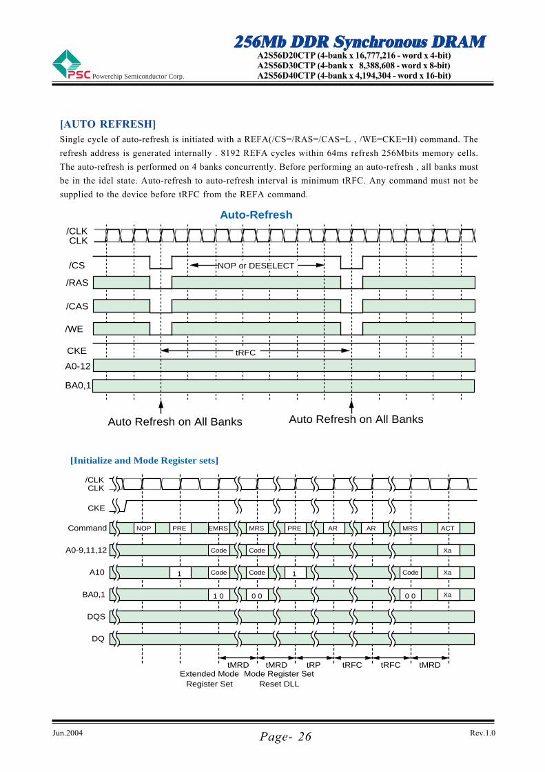
[AUTO REFRESH]Single cycle of auto-refresh is initiated with a REFA(/CS=/RAS=/CAS=L , /WE=CKE=H) command. The
refresh address is generated internally . 8192 REFA cycles within 64ms refresh 256Mbits memory cells.
The auto-refresh is performed on 4 banks concurrently. Before performing an auto-refresh , all banks must
be in the idel state. Auto-refresh to auto-refresh interval is minimum tRFC. Any command must not be
supplied to the device before tRFC from the REFA command.
[Initialize and Mode Register sets]
Command
/CLKCLK
EMRSPRENOP MRS PRE AR AR MRS ACT
Code Code Xa
Code Xa
1 0 Xa
A0-9,11,12
A10 Code1
BA0,1
DQS
DQ
1
0 0 0 0
Code
tMRD tMRD tRP tRFC tRFC tMRD
CKE
Extended ModeRegister Set
Mode Register SetReset DLL
/RAS
CKE
/CS
/CAS
/WE
A0-12
BA0,1
NOP or DESELECT
tRFC
Auto Refresh on All Banks Auto Refresh on All Banks
/CLKCLK
Auto-Refresh
Jun.2004 Rev.1.0
256Mb DDR Synchronous DRAM256Mb DDR Synchronous DRAM256Mb DDR Synchronous DRAM256Mb DDR Synchronous DRAM256Mb DDR Synchronous DRAM
Powerchip Semiconductor Corp.
A2S56D20CTP (4-bank x 16,777,216 - word x 4-bit)A2S56D30CTP (4-bank x 8,388,608 - word x 8-bit)A2S56D40CTP (4-bank x 4,194,304 - word x 16-bit)
Page- 27
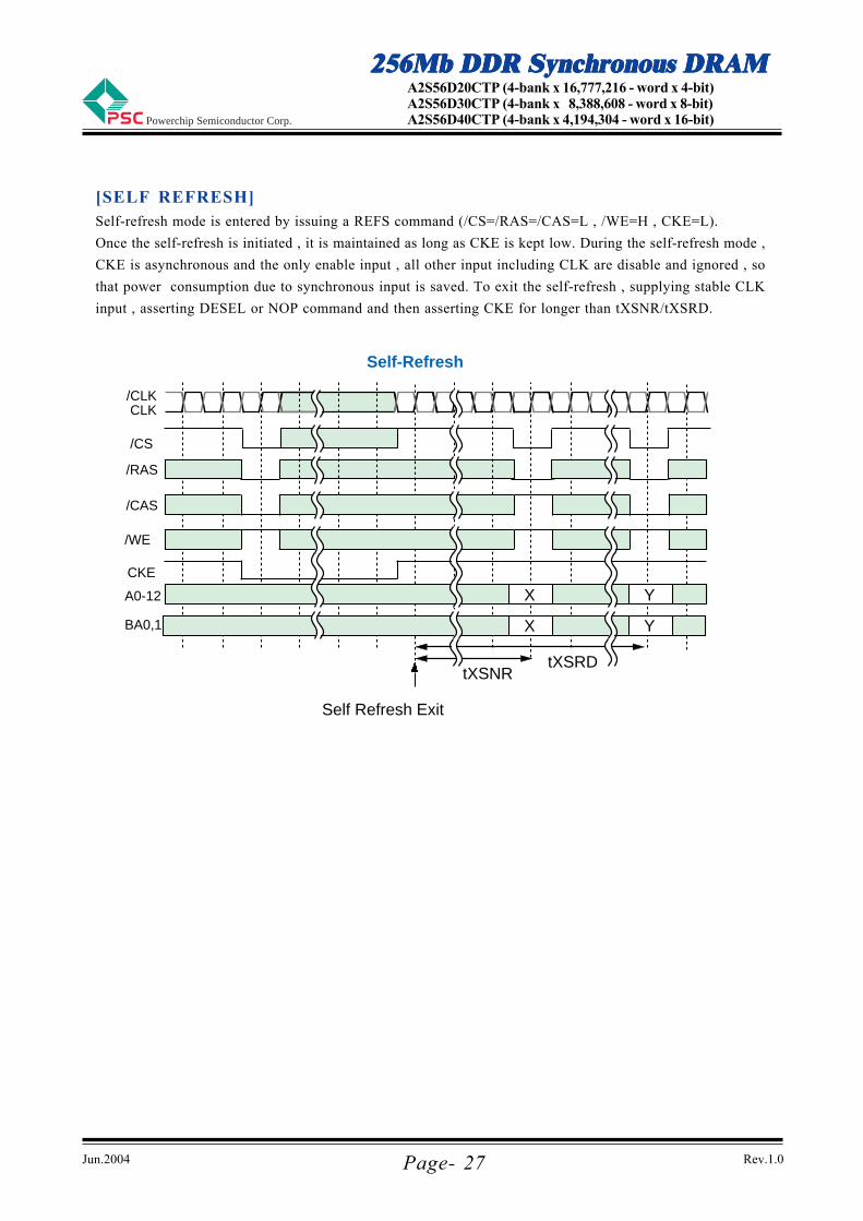
[SELF REFRESH]Self-refresh mode is entered by issuing a REFS command (/CS=/RAS=/CAS=L , /WE=H , CKE=L).
Once the self-refresh is initiated , it is maintained as long as CKE is kept low. During the self-refresh mode ,
CKE is asynchronous and the only enable input , all other input including CLK are disable and ignored , so
that power consumption due to synchronous input is saved. To exit the self-refresh , supplying stable CLK
input , asserting DESEL or NOP command and then asserting CKE for longer than tXSNR/tXSRD.
/RAS
CKE
/CS
/CAS
/WE
A0-12
BA0,1
tXSNR
Self Refresh Exit
/CLKCLK
X Y
X Y
tXSRD
Self-Refresh
Jun.2004 Rev.1.0
256Mb DDR Synchronous DRAM256Mb DDR Synchronous DRAM256Mb DDR Synchronous DRAM256Mb DDR Synchronous DRAM256Mb DDR Synchronous DRAMA2S56D20CTP (4-bank x 16,777,216 - word x 4-bit)A2S56D30CTP (4-bank x 8,388,608 - word x 8-bit)A2S56D40CTP (4-bank x 4,194,304 - word x 16-bit)Powerchip Semiconductor Corp.
Page- 28
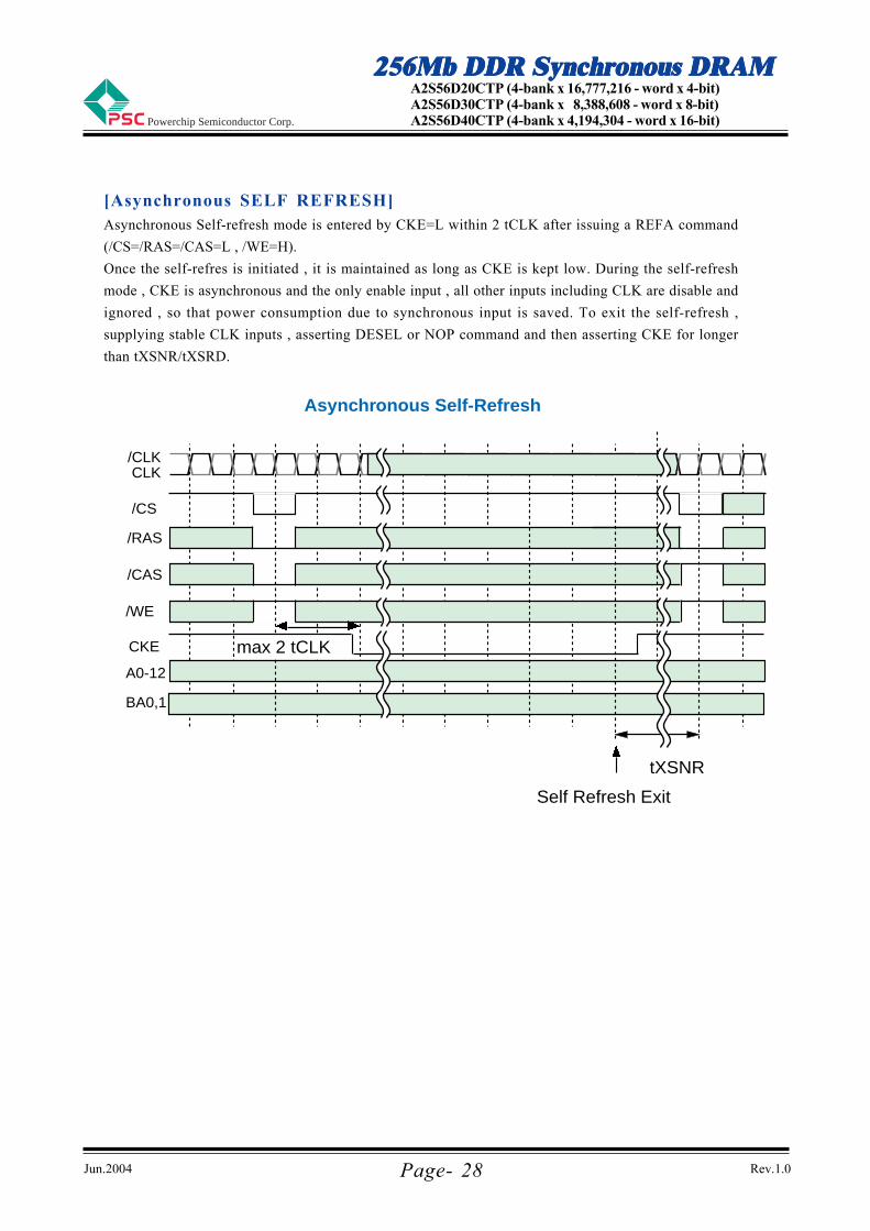
[Asynchronous SELF REFRESH]Asynchronous Self-refresh mode is entered by CKE=L within 2 tCLK after issuing a REFA command
(/CS=/RAS=/CAS=L , /WE=H).
Once the self-refres is initiated , it is maintained as long as CKE is kept low. During the self-refresh
mode , CKE is asynchronous and the only enable input , all other inputs including CLK are disable and
ignored , so that power consumption due to synchronous input is saved. To exit the self-refresh ,
supplying stable CLK inputs , asserting DESEL or NOP command and then asserting CKE for longer
than tXSNR/tXSRD.
/RAS
CKE
/CS
/CAS
/WE
A0-12
BA0,1
tXSNR
Self Refresh Exit
max 2 tCLK
/CLKCLK
Asynchronous Self-Refresh
Jun.2004 Rev.1.0
256Mb DDR Synchronous DRAM256Mb DDR Synchronous DRAM256Mb DDR Synchronous DRAM256Mb DDR Synchronous DRAM256Mb DDR Synchronous DRAM
Powerchip Semiconductor Corp.
A2S56D20CTP (4-bank x 16,777,216 - word x 4-bit)A2S56D30CTP (4-bank x 8,388,608 - word x 8-bit)A2S56D40CTP (4-bank x 4,194,304 - word x 16-bit)
/CLKCLK
Command PRE
CKE
Command ACT
CKE
Standby Power Down
Active Power Down
NOP
NOP
Command
DQS
DQ
DM
Write READ
D0 D1 D3 D4 D5 D6 D7
masked by DM=H
Don't Care
Q2 Q3 Q4 Q5
/CLKCLK
Q0 Q1 Q6
Valid
NOP
NOP
ValidtXPNR/tXPRD
Power Down by CKE
DM Function(BL=8 , CL=2)
Page- 29
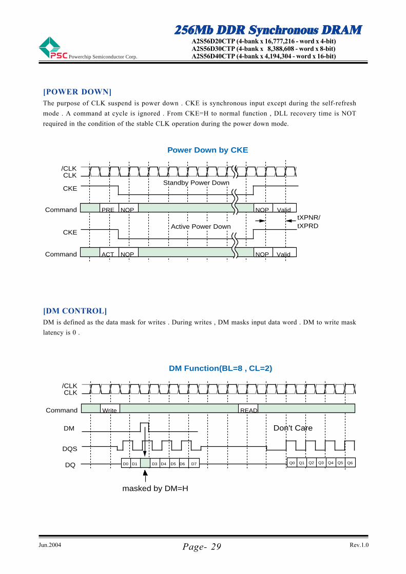
[POWER DOWN]The purpose of CLK suspend is power down . CKE is synchronous input except during the self-refresh
mode . A command at cycle is ignored . From CKE=H to normal function , DLL recovery time is NOT
required in the condition of the stable CLK operation during the power down mode.
[DM CONTROL]DM is defined as the data mask for writes . During writes , DM masks input data word . DM to write mask
latency is 0 .
Jun.2004 Rev.1.0
256Mb DDR Synchronous DRAM256Mb DDR Synchronous DRAM256Mb DDR Synchronous DRAM256Mb DDR Synchronous DRAM256Mb DDR Synchronous DRAMA2S56D20CTP (4-bank x 16,777,216 - word x 4-bit)A2S56D30CTP (4-bank x 8,388,608 - word x 8-bit)A2S56D40CTP (4-bank x 4,194,304 - word x 16-bit)Powerchip Semiconductor Corp.
Page- 30
/CLK
DQS
tIS tIH
VREF
CLK
Valid Data
/QFC
Read Operation
tAC
tDQSCK
tCLtCHtCK
tDQSQtQH
tRPRE tRPST
DQS
/QFC
/CLK
CLKtDQSS
tDS tDH
tDQSL tDQSHtWPRE
Write Operation / tDQSS=max.
tDSStWPRES
tWPST
tQCKtQOH(min)
tQPREtQPST
DQS
/QFC
/CLK
CLKtDQSS
tDS tDH
tDQSL tDQSHtWPRE
Write Operation / tDQSS=min.
tDSH
tWPREStWPST
tQCKtQOH(max)
DQ
DQ
DQ
Cmd &Add.
Jun.2004 Rev.1.0
256Mb DDR Synchronous DRAM256Mb DDR Synchronous DRAM256Mb DDR Synchronous DRAM256Mb DDR Synchronous DRAM256Mb DDR Synchronous DRAM
Powerchip Semiconductor Corp.
A2S56D20CTP (4-bank x 16,777,216 - word x 4-bit)A2S56D30CTP (4-bank x 8,388,608 - word x 8-bit)A2S56D40CTP (4-bank x 4,194,304 - word x 16-bit)
Page- 31
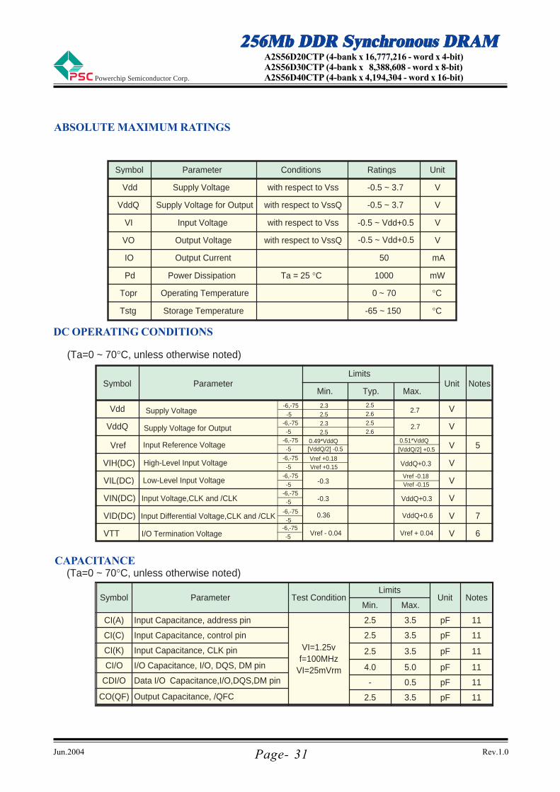
ABSOLUTE MAXIMUM RATINGS
CAPACITANCE
DC OPERATING CONDITIONS
(Ta=0 ~ 70°C, unless otherwise noted)
Symbol Parameter Conditions Ratings Unit
Vdd Supply Voltage with respect to Vss -0.5 ~ 3.7 V
VddQ Supply Voltage for Output with respect to VssQ -0.5 ~ 3.7 V
VI Input Voltage with respect to Vss -0.5 ~ Vdd+0.5 V
VO Output Voltage with respect to VssQ V
IO Output Current 50 mA
Pd Power Dissipation Ta = 25 °C 1000 mW
Topr Operating Temperature 0 ~ 70 °C
Tstg Storage Temperature -65 ~ 150 °C
Symbol ParameterLimits
UnitMin. Typ. Max.
Vdd
Supply Voltage for Output
V
VddQ V
VIH(DC)
Low-Level Input Voltage
Vref +0.18 VddQ+0.3 V
VIL(DC) -0.3Vref -0.18
V
Data I/O Capacitance,I/O,DQS,DM pinCDI/O 11pF0.5-
11pF3.52.5CO(QF) Output Capacitance, /QFC
11pF5.04.0
11pF3.52.5
11pF3.52.5
11pF3.52.5
I/O Capacitance, I/O, DQS, DM pinCI/O
Input Capacitance, CLK pinCI(K)
Input Capacitance, control pinCI(C)
Input Capacitance, address pinCI(A)
VI=1.25vf=100MHz
VI=25mVrm
NotesUnitMax.Min.
LimitsTest ConditionParameterSymbol
Vref Input Reference Voltage 0.49*VddQ 0.51*VddQV
VIN(DC)
Input Differential Voltage,CLK and /CLK
-0.3 VddQ+0.3 V
VID(DC) VddQ+0.6 V
VTT I/O Termination Voltage VVref + 0.04
Notes
6
5
7
-0.5 ~ Vdd+0.5
2.3Supply Voltage
High-Level Input Voltage
Input Voltage,CLK and /CLK
2.5
2.52.6
-6,-75-5
-6,-75-5
-6,-75-5
2.32.5
2.52.6
[VddQ/2] -0.5 [VddQ/2] +0.5-6,-75-5 Vref +0.15
-6,-75-5 Vref -0.15
-6,-75-5
-6,-75-5
-6,-75-5 Vref - 0.04
2.7
2.7
0.36
(Ta=0 ~ 70°C, unless otherwise noted)
Jun.2004 Rev.1.0
256Mb DDR Synchronous DRAM256Mb DDR Synchronous DRAM256Mb DDR Synchronous DRAM256Mb DDR Synchronous DRAM256Mb DDR Synchronous DRAMA2S56D20CTP (4-bank x 16,777,216 - word x 4-bit)A2S56D30CTP (4-bank x 8,388,608 - word x 8-bit)A2S56D40CTP (4-bank x 4,194,304 - word x 16-bit)Powerchip Semiconductor Corp.
Page- 32
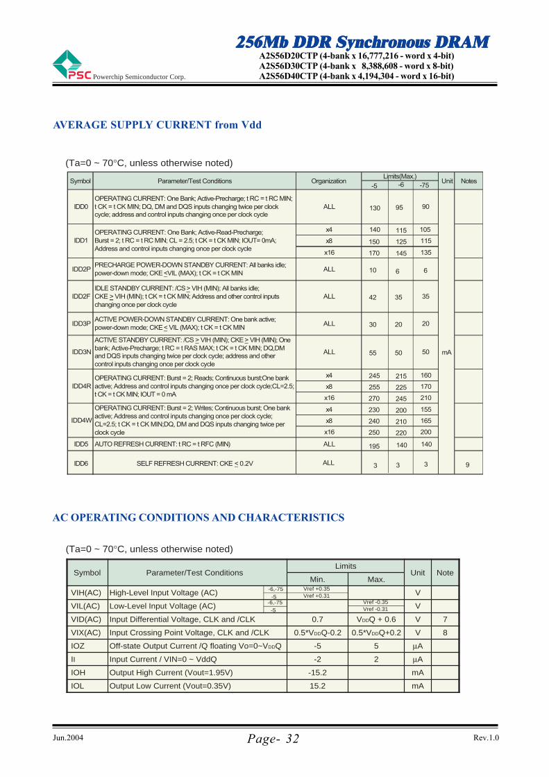
AVERAGE SUPPLY CURRENT from Vdd
AC OPERATING CONDITIONS AND CHARACTERISTICS
-75
x4
x8
x16
x4
x8
x16
x4
x8
x16
IDD5 AUTO REFRESH CURRENT: t RC = t RFC (MIN) ALL
ALL IDD6 SELF REFRESH CURRENT: CKE < 0.2V
ALL
IDD4W
OPERATING CURRENT: Burst = 2; Writes; Continuous burst; One bankactive; Address and control inputs changing once per clock cycle;CL=2.5; t CK = t CK MIN;DQ, DM and DQS inputs changing twice perclock cycle
ALL
ALL IDD3PACTIVE POWER-DOWN STANDBY CURRENT: One bank active;power-down mode; CKE < VIL (MAX); t CK = t CK MIN
ACTIVE STANDBY CURRENT: /CS > VIH (MIN); CKE > VIH (MIN); Onebank; Active-Precharge; t RC = t RAS MAX; t CK = t CK MIN; DQ,DMand DQS inputs changing twice per clock cycle; address and othercontrol inputs changing once per clock cycle
IDD3N ALL
IDD4ROPERATING CURRENT: Burst = 2; Reads; Continuous burst;One bankactive; Address and control inputs changing once per clock cycle;CL=2.5;t CK = t CK MIN; IOUT = 0 mA
mA
PRECHARGE POWER-DOWN STANDBY CURRENT: All banks idle;power-down mode; CKE <VIL (MAX); t CK = t CK MIN
OrganizationParameter/Test Conditions
OPERATING CURRENT: One Bank; Active-Precharge; t RC = t RC MIN;t CK = t CK MIN; DQ, DM and DQS inputs changing twice per clockcycle; address and control inputs changing once per clock cycle
UnitLimits(Max.)
ALL
IDD2P
IDD2FIDLE STANDBY CURRENT: /CS > VIH (MIN); All banks idle;CKE > VIH (MIN); t CK = t CK MIN; Address and other control inputschanging once per clock cycle
Notes
IDD0
IDD1OPERATING CURRENT: One Bank; Active-Read-Precharge;Burst = 2; t RC = t RC MIN; CL = 2.5; t CK = t CK MIN; IOUT= 0mA;Address and control inputs changing once per clock cycle
Symbol
8
7
mA
mA
µA
µA
V
V
V
V
NoteUnit
15.2
-15.2
2-2
5-5
0.5*VDDQ+0.20.5*VDDQ-0.2
VDDQ + 0.60.7
Vref -0.35
Vref +0.35
Max.Min.
Limits
Output Low Current (Vout=0.35V)
Output High Current (Vout=1.95V)
Input Current / VIN=0 ~ VddQ
Off-state Output Current /Q floating Vo=0~VDDQ
Input Crossing Point Voltage, CLK and /CLK
Input Differential Voltage, CLK and /CLK
Low-Level Input Voltage (AC)
High-Level Input Voltage (AC)
Parameter/Test Conditions
II
IOL
IOH
IOZ
VIX(AC)
VID(AC)
VIL(AC)
VIH(AC)
Symbol
105
115
135
160
170
210
155
165
200
3
50
35
20
90
6
140
-6
115
125
145
215
225
245
200
210
220
3
50
35
20
95
6
140
9
10
42
30
55
245
255
270
230
240
250
150
170
130
140
195
3
-5
-6,-75-5
-6,-75-5 Vref -0.31
Vref +0.31
(Ta=0 ~ 70°C, unless otherwise noted)
(Ta=0 ~ 70°C, unless otherwise noted)
Jun.2004 Rev.1.0
256Mb DDR Synchronous DRAM256Mb DDR Synchronous DRAM256Mb DDR Synchronous DRAM256Mb DDR Synchronous DRAM256Mb DDR Synchronous DRAM
Powerchip Semiconductor Corp.
A2S56D20CTP (4-bank x 16,777,216 - word x 4-bit)A2S56D30CTP (4-bank x 8,388,608 - word x 8-bit)A2S56D40CTP (4-bank x 4,194,304 - word x 16-bit)
Page- 33
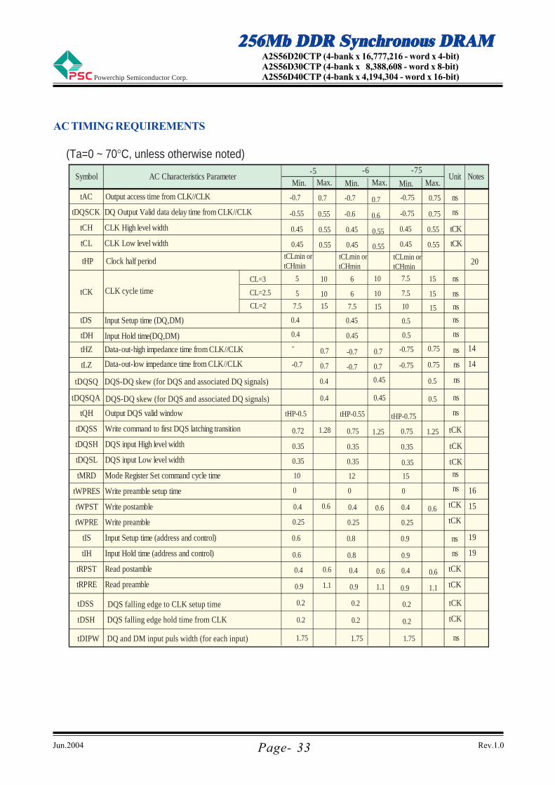
AC TIMING REQUIREMENTS
Max. Min.
tAC Output access time from CLK//CLK
tDQSCK DQ Output Valid data delay time from CLK//CLK
tCH CLK High level width
tCL CLK Low level width
tDH
Input Setup time (DQ,DM)tDS
Input Hold time(DQ,DM)
tHZ Data-out-high impedance time from CLK//CLK 14
tLZ Data-out-low impedance time from CLK//CLK 14
tDQSQ DQS-DQ skew (for DQS and associated DQ signals)
tHP Clock half period
tQH Output DQS valid window
tDQSS Write command to first DQS latching transition
tDQSH DQS input High level width
tDQSL DQS input Low level width
tMRD Mode Register Set command cycle time
tWPRES Write preamble setup time
tWPST Write postamble
tWPRE Write preamble
tIS Input Setup time (address and control)
tIH Input Hold time (address and control)
16
15
19
19
tRPST Read postamble
tRPRE Read preamble
Unit Notes
tCK CLK cycle time
Symbol AC Characteristics Parameter-6
Max.Min.
ns
ns
ns
ns
tCK
tCK
ns
ns
ns
ns
ns
ns
ns
tCK
tCK
tCK
tCK
tCK
tCK
tCK
ns
ns
-75
Min. Max.
tCLmin or tCHmin
-0.75
-0.75
0.45
0.45
0.75
0.75
0.55
0.55
ns
nsCL=2.5 7.5 15
DQS-DQ skew (for DQS and associated DQ signals)tDQSQA
tDSS
tDSH
DQS falling edge to CLK setup time
DQS falling edge hold time from CLK
tDIPW DQ and DM input puls width (for each input)
tCK
tCK
ns
20
CL=2
0.55
0.55
0.4
0.7
0.7
0.6
1.28
0.6
1.1
10
0.7
0.55
0.4
15 10 15
tHP-0.5
tCLmin or tCHmin
0.45
0.45
0.4
0.4
-
-0.7
0.35
0.35
0.4
0
10
0.25
0.6
0.6
0.72
0.4
5
-0.7
-0.55
1.75
0.2
0.2
0.9
7.5
0.5
0.75
0.75
0.6
1.25
0.6
1.1
0.5
tHP-0.75
0.5
0.5
-0.75
-0.75
0.35
0.4
0
15
0.25
0.9
0.9
0.75
0.4
1.75
0.35
0.2
0.2
0.9
-5
tHP-0.55
tCLmin or tCHmin
0.45
0.45
0.45
0.45
-0.7
-0.7
0.35
0.35
0.4
0
12
0.25
0.8
0.8
0.75
0.4
6
-0.7
-0.6
1.75
0.2
0.2
0.9
7.5
0.55
0.55
0.45
0.7
0.7
0.6
1.25
0.6
1.1
10
0.7
0.6
0.45
15
(Ta=0 ~ 70°C, unless otherwise noted)
CL=3 ns7.5 15105 6 10
Jun.2004 Rev.1.0
256Mb DDR Synchronous DRAM256Mb DDR Synchronous DRAM256Mb DDR Synchronous DRAM256Mb DDR Synchronous DRAM256Mb DDR Synchronous DRAMA2S56D20CTP (4-bank x 16,777,216 - word x 4-bit)A2S56D30CTP (4-bank x 8,388,608 - word x 8-bit)A2S56D40CTP (4-bank x 4,194,304 - word x 16-bit)Powerchip Semiconductor Corp.
Page-34
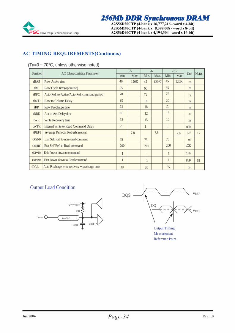
AC TIMING REQUIREMENTS(Continous)
Min. Max. Max.
tRAS Row Active time
tRC Row Cycle time(operation)
tRFC Auto Ref. to Active/Auto Ref. command period
tRCD Row to Column Delay
tRP Row Precharge time
tRRD Act to Act Delay time
tWR Write Recovery time
tWTR Internal Write to Read Command Delay
tREFI Average Periodic Refresh interval µ
Unit NotesSymbol AC Characteristics Parameter-5
Output Load Condition
DQ
Output Timing MeasurementReference Point
VREF
VREF
DQS
VOUT
VREF30pF
50Ω
VTT=VREF
Zo=50Ω
s
tCK
ns
ns
ns
ns
ns
ns
ns
-6 -75Min. Max. Min.
120K 120K 120K
7.8 7.8 7.8
tXSNR Exit Self Ref. to non-Read command
tXSRD Exit Self Ref. to Read command tCK
ns
tXPNR Exit Power down to command
tXPRD Exit Power down to Read command
tDAL Auto Precharge write recovery + precharge time
40
55
70
15
15
10
15
2
75
200
1
1
30 ns
tCK
tCK
17
18
45
65
75
20
20
15
15
1
75
200
1
1
35
42
60
72
18
18
12
15
1
75
200
1
1
30
(Ta=0 ~ 70°C, unless otherwise noted)
Jun.2004 Rev.1.0
256Mb DDR Synchronous DRAM256Mb DDR Synchronous DRAM256Mb DDR Synchronous DRAM256Mb DDR Synchronous DRAM256Mb DDR Synchronous DRAM
Powerchip Semiconductor Corp.
A2S56D20CTP (4-bank x 16,777,216 - word x 4-bit)A2S56D30CTP (4-bank x 8,388,608 - word x 8-bit)A2S56D40CTP (4-bank x 4,194,304 - word x 16-bit)
Page- 3 5
NOTES:NOTES:NOTES:NOTES:NOTES:1. All voltages referenced to Vss.2. Tests for AC timing, IDD, and electrical, AC and DC characteristics, may be conducted at nominal reference/supply
voltage levels, but the related specifications and device operation are guaranteed for the full voltage range specified.3. AC timing and IDD tests may use a VIL to VIH swing of up to 1.5V in the test environment, but input timing is still
referenced to VREF (or to the crossing point for CK//CK), and parameter specifications are guaranteed for the specified AC input levels under normal use conditions. The minimum slew rate for the input signals is 1V/ns in the range between VIL(AC) and VIH(AC).
4. The AC and DC input level specifications are as defined in the SSTL_2 Standard (i.e. the receiver will effectively switch as a result of the signal crossing the AC input level, and will remain in that state as long as the signal does not ring back above (below) the DC input LOW (HIGH) level.
5. VREF is expected to be equal to 0.5*VddQ of the transmitting device, and to track variations in the DC level of the same. Peak-to-peak noise on VREF may not exceed +/-2% of the DC value.
6. VTT is not applied directly to the device. VTT is a system supply for signal termination resistors, is expected to be set equal to VREF, and must track variations in the DC level of VREF.
7. VID is the magnitude of the difference between the input level on CLK and the input level on /CLK.8. The value of VIX is expected to equal 0.5*VddQ of the transmitting device and must track variations in the DC level of
the same.9. Enables on-chip refresh and address counters.10. IDD specifications are tested after the device is properly initialized.11. This parameter is sampled. VddQ = +2.5V ±0.2V, Vdd = +2.5V ±0.2V , f = 100 MHz, Ta = 25°C, VOUT(DC) =
VddQ/2, VOUT(PEAK TO PEAK) = 25mV. DM inputs are grouped with I/O pins - reflecting the fact that they are matched in loading (to facilitate trace matching at the board level).
12. The CLK//CLK input reference level (for timing referenced to CLK//CLK) is the point at which CLK and /CLK cross; the input reference level for signals other than CLK//CLK, is VREF.
13. Inputs are not recognized as valid until VREF stabilizes. Exception: during the period before VREF stabilizes, CKE =< 0.3VddQ is recognized as LOW.
14. t HZ and tLZ transitions occur in the same access time windows as valid data transitions. These parameters are not referenced to a specific voltage level, but specify when the device output is no longer driving (HZ), or begins driving (LZ).
15. The maximum limit for this parameter is not a device limit. The device will operate with a greater value for this parameter, but system performance (bus turnaround) will degrade accordingly.
16. The specific requirement is that DQS be valid (HIGH, LOW, or at some point on a valid transition) on or before this CLK edge. A valid transition is defined as monotonic, and meeting the input slew rate specifications of the device. When no writes were previously in progress on the bus, DQS will be transitioning from High-Z to logic LOW. If a previous write was in progress, DQS could be HIGH, LOW, or transitioning from HIGH to LOW at this time, depending on tDQSS.
17. A maximum of eight AUTO REFRESH commands can be posted to any given DDR SDRAM device. 18. tXPRD should be 200 tCLK in the condition of the unstable CLK operation during the power down mode.19. For command/address and CK & /CK slew rate ≥ 1.0V/ns.20. Min (tCL,tCH) refers to the smaller of the actual clock low time and the actual clock high time as provided to the
device.