Embed Size (px)
Citation preview

Integrated Silicon Solution, Inc. 1Rev. A1/31/2013
IS41C16256CIS41LV16256C
Copyright © 2013 Integrated Silicon Solution, Inc. All rights reserved. ISSI reserves the right to make changes to this specification and its products at any time without notice. ISSI assumes no liability arising out of the application or use of any information, products or services described herein. Customers are advised to obtain the lat-est version of this device specification before relying on any published information and before placing orders for products.
Integrated Silicon Solution, Inc. does not recommend the use of any of its products in life support applications where the failure or malfunction of the product can reasonably be ex-pected to cause failure of the life support system or to significantly affect its safety or effectiveness. Products are not authorized for use in such applications unless Integrated Silicon Solution, Inc. receives written assurance to its satisfaction, that:a.) the risk of injury or damage has been minimized;b.) the user assume all such risks; andc.) potential liability of Integrated Silicon Solution, Inc is adequately protected under the circumstances
FEATURES
• TTLcompatibleinputsandoutputs;tri-stateI/O
• RefreshInterval:512cycles/8ms
• RefreshMode:RAS-Only,CAS-before-RAS(CBR),and Hidden
• JEDECstandardpinout
• Singlepowersupply: 5V±10%(IS41C16256C)
3.3V±10%(IS41LV16256C)
• ByteWriteandByteReadoperationviatwoCAS
• IndustrialTemperatureRange-40°Cto+85°C
DESCRIPTION
TheIS41C16256CandIS41LV16256Care262,144x16-bithigh-performanceCMOSDynamicRandomAccessMemo-ries. BothproductsofferacceleratedcycleaccessEDOPageMode.EDOPageModeallows512randomaccesseswithinasinglerowwithaccesscycletimeasshortas14nsper16-bitword.Itisasynchronous,asitdoesnotrequireaclocksignalinputtosynchronizecommandsandI/O.
ThesefeaturesmaketheIS41C/LV16256Cideally suited for high band-width graphics, digital signal processing, high-performance computing systems, and peripheral applications thatrunwithoutaclocktosynchronizewiththeDRAM.
TheIS41C/LV16256Cispackagedin40-pinTSOP(TypeII).
256Kx164Mb DRAM WITH EDO PAGE MODE
KEY TIMING PARAMETERS
Parameter -35 Unit
Max.RASAccessTime(trac) 35 ns
Max.CASAccessTime(tcac) 13 ns
Max.ColumnAddressAccessTime(taa) 18 ns
Min.EDOPageModeCycleTime(tpc) 14 ns
Min.Read/WriteCycleTime(trc) 60 ns
JANUARY 2013

2 Integrated Silicon Solution, Inc. Rev. A
1/31/2013
IS41C16256CIS41LV16256C
PIN CONFIGURATIONS40-Pin TSOP (Type II)
PIN DESCRIPTIONS
A0-A8 AddressInputs
I/O0-15 DataInputs/Outputs
WE WriteEnable
OE OutputEnable
RAS RowAddressStrobe
UCAS Upper Column Address Strobe
LCAS LowerColumnAddressStrobe
Vdd Power
GND Ground
NC No Connection
1
2
3
4
5
6
7
8
9
10
11
12
13
14
15
16
17
18
19
20
40
39
38
37
36
35
34
33
32
31
30
29
28
27
26
25
24
23
22
21
VDD
I/O0
I/O1
I/O2
I/O3
VDD
I/O4
I/O5
I/O6
I/O7
NC
NC
WE
RAS
NC
A0
A1
A2
A3
VDD
GND
I/O15
I/O14
I/O13
I/O12
GND
I/O11
I/O10
I/O9
I/O8
NC
LCAS
UCAS
OE
A8
A7
A6
A5
A4
GND
Integrated Silicon Solution, Inc. 3Rev. A1/31/2013
IS41C16256CIS41LV16256C
FUNCTIONAL BLOCK DIAGRAM
OE
WE
LCAS
UCASCAS WE
OE
DATA I/O BUS
COLUMN DECODERS
SENSE AMPLIFIERS
MEMORY ARRAY262,144 x 16
RO
W D
EC
OD
ER DA
TA
I/O
BU
FF
ER
S
CAS CLOCK
GENERATOR
WE CONTROLLOGICS
OE CONTROL
LOGIC
I/O0-I/O15
RAS RAS
A0-A8
RAS CLOCK
GENERATOR
REFRESH COUNTER
ADDRESSBUFFERS

4 Integrated Silicon Solution, Inc. Rev. A
1/31/2013
IS41C16256CIS41LV16256C
TRUTH TABLE(5)
Function RAS LCAS UCAS WE OE Address tR/tC I/O
Standby H X X X X X High-Z
Read:Word L L L H L ROW/COL Dout
Read:LowerByte L L H H L ROW/COL LowerByte,Dout Upper Byte, High-Z
Read:UpperByte L H L H L ROW/COL LowerByte,High-Z UpperByte,Dout
Write:Word(EarlyWrite) L L L L X ROW/COL Din
Write:LowerByte(EarlyWrite) L L H L X ROW/COL LowerByte,Din Upper Byte, High-Z
Write:UpperByte(EarlyWrite) L H L L X ROW/COL LowerByte,High-Z UpperByte,Din
Read-Write(1,2) L L L H→L L→H ROW/COL Dout,Din
EDOPage-ModeRead(2) 1stCycle: L H→L H→L H L ROW/COL Dout 2ndCycle: L H→L H→L H L NA/COL Dout AnyCycle: L L→H L→H H L NA/NA Dout
EDOPage-ModeWrite(1) 1stCycle: L H→L H→L L X ROW/COL Din 2ndCycle: L H→L H→L L X NA/COL Din
EDOPage-Mode 1stCycle: L H→L H→L H→L L→H ROW/COL Dout,Din Read-Write(1,2) 2ndCycle: L H→L H→L H→L L→H NA/COL Dout,Din
HiddenRefresh Read(2) L→H→L L L H L ROW/COL Dout Write(1,3) L→H→L L L L X ROW/COL Dout
RAS-OnlyRefresh L H H X X ROW/NA High-Z
CBRRefresh(4) H→L L L H X X High-ZNotes: 1. TheseWRITEcyclesmayalsobeBYTEWRITEcycles(eitherLCAS or UCAS active).2. TheseREADcyclesmayalsobeBYTEREADcycles(eitherLCAS or UCAS active).3.Earlywriteonly.4. AtleastoneofthetwoCAS signals must be active (LCAS or UCAS).5.Commandsvalidonlyafterproperintialization.

Integrated Silicon Solution, Inc. 5Rev. A1/31/2013
IS41C16256CIS41LV16256C
Functional DescriptionTheIS41C/LV16256CisaCMOSDRAMoptimizedforhigh-speedbandwidth,lowpowerapplications.DuringREADorWRITEcycles,eachbitisuniquelyaddressedthroughthe18addressbits.Theseareenteredninebits(A0-A8)atatime.TherowaddressislatchedbytheRowAddressStrobe(RAS).Thecolumnaddressis latched by the Column Address Strobe (CAS). RAS is used to latch the first nine bits and CAS is used the latter nine bits.TheIS41C/LV16256ChastwoCAS controls, LCAS and UCAS.TheLCAS and UCAS inputs internally gener-ates a CAS signal functioning in an identical manner to the single CASinputontheother256Kx16DRAMs.ThekeydifferenceisthateachCAS controls its corre-spondingI/Otristatelogic(inconjunctionwithOE and WE and RAS). LCAScontrolsI/O0throughI/O7andUCAScontrolsI/O8throughI/O15.TheIS41C/LV16256CCAS function is determined by the first CAS (LCAS or UCAS)transitioningLOWandthelasttransitioningbackHIGH.ThetwoCAS controls givetheIS41C/LV16256CbothBYTEREADandBYTEWRITEcyclecapabilities.
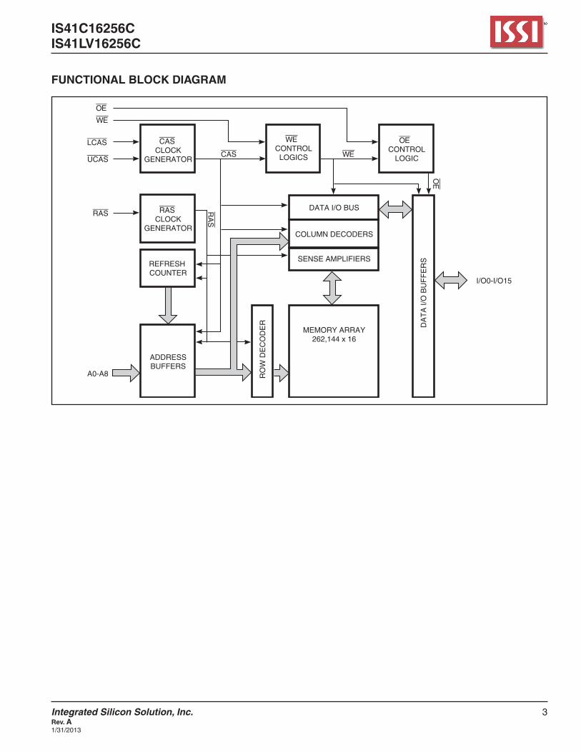
Memory CycleA memory cycle is initiated by bring RASLOWanditis terminated by returning both RAS and CAS HIGH. Toensuresproperdeviceoperationanddataintegrityany memory cycle, once initiated, must not be ended or aborted before the minimum tras time has expired. A new cycle must not be initiated until the minimum precharge time trp, tcp has elapsed. Read CycleA read cycle is initiated by the falling edge of CAS or OE, whichever occurs last, while holding WE HIGH. Thecolumnaddressmustbeheldforaminimumtimespecified by tar.DataOutbecomesvalidonlywhentrac, taa, tcac and toea are all satisfied. As a result, the access time is dependent on the timing relationships between these parameters.
Write CycleA write cycle is initiated by the falling edge of CAS and WE,whicheveroccurslast.Theinputdatamustbevalid at or before the falling edge of CAS or WE, which-ever occurs last.
Refresh CycleToretaindata,512refreshcyclesarerequiredineach 8msperiod.Therearetwowaystorefreshthememo-ry.1. Byclockingeachofthe512rowaddresses(A0throughA8)withRASatleastonceevery8ms.Anyread, write, read-modify-write or RAS-only cycle re-freshes the addressed row.2. Using a CAS-before-RAS refresh cycle. CAS-before-RAS refresh is activated by the falling edge of RAS, while holding CASLOW.InCAS-before-RAS refresh cycle, an internal 9-bit counter provides the row ad-dresses and the external address inputs are ignored.CAS-before-RAS is a refresh-only mode and no data accessordeviceselectionisallowed.Thus,theoutputremains in the High-Z state during the cycle.
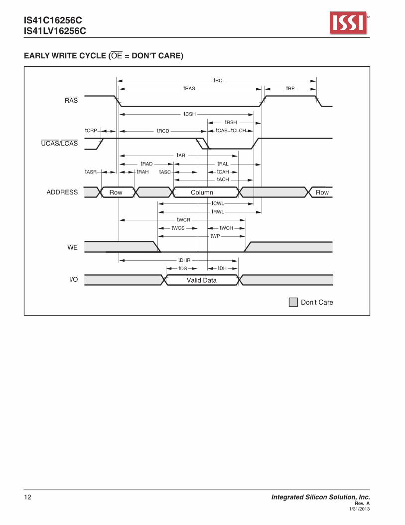
Extended Data Out Page ModeEDOpagemodeoperationpermitsall512columnswithin a selected row to be randomly accessed at a high data rate. InEDOpagemodereadcycle,thedata-outisheldtothe next CAS cycle’s falling edge, instead of the ris-ing edge. For this reason, the valid data output time inEDOpagemodeisextendedcomparedwiththefast page mode. In the fast page mode, the valid data output time becomes shorter as the CAS cycle time becomesshorter.Therefore,inEDOpagemode,thetiming margin in read cycle is larger than that of the fast page mode even if the CAS cycle time becomes shorter.InEDOpagemode,duetotheextendeddatafunction,the CAS cycle time can be shorter than in the fast page mode if the timing margin is the same. TheEDOpagemodeallowsbothreadandwriteopera-tions during one RAS cycle, but the performance is equivalent to that of the fast page mode in that case.
Power-OnDuringPower-on,RAS, CAS, UCAS, LCAS, and WE mustalltrackwithVdd (HIGH) to avoid current surges, and allow initialization to continue. An inital pause of 200 µs is required followed by a minimum of eight ini-tialization cycles (any combination of cycles containing a RAS signal).

6 Integrated Silicon Solution, Inc. Rev. A
1/31/2013
IS41C16256CIS41LV16256C
ABSOLUTE MAXIMUM RATINGS(1)
Symbol Parameters Rating Unit
Vt VoltageonAnyPinRelativetoGND 5V -1.0to+7.0 V 3.3V -0.5to+4.6 V Vdd SupplyVoltage 5V -1.0to+7.0 V 3.3V -0.5to+4.6 V Iout OutputCurrent 50 mA Pd PowerDissipation 1 W Ta OperationTemperature -40to+85 °C Tstg StorageTemperature –55to+125 °CNote:1. StressgreaterthanthoselistedunderABSOLUTEMAXIMUMRATINGSmaycausepermanent
damagetothedevice.Thisisastressratingonlyandfunctionaloperationofthedeviceattheseor any other conditions above those indicated in the operational sections of this specification is notimplied.Exposuretoabsolutemaximumratingconditionsforextendedperiodsmayaffectreliability.
CAPACITANCE(1,2)
Symbol Parameter Max. Unit
Cin1 InputCapacitance:A0-A8 5 pF
Cin2 Input Capacitance: RAS, UCAS, LCAS, WE, OE 7 pF
Cio DataInput/OutputCapacitance:I/O0-I/O15 7 pFNotes:1.Testedinitiallyandafteranydesignorprocesschangesthatmayaffecttheseparameters.2.Testconditions:Ta=25°C,f=1MHz,
RECOMMENDED OPERATING CONDITIONS (VoltagesarereferencedtoGND.)
Symbol Parameter Test Conditions Min. Typ. Max. Unit
Vdd SupplyVoltage 5V 4.5 5.0 5.5 V 3.3V 3.0 3.3 3.6 V Vih InputHighVoltage 5V 2.4 — Vdd +1.0 V 3.3V 2.0 — Vdd +0.3 V Vil InputLowVoltage 5V –1.0 — 0.8 V 3.3V –0.3 — 0.8 V iil InputLeakageCurrent Anyinput0V≤Vin ≤Vdd -5 5 µA Otherinputsnotundertest=0V
iio OutputLeakageCurrent Outputisdisabled(Hi-Z) -5 5 µA 0V≤ Vout ≤Vdd
Voh OutputHighVoltageLevel ioh=–5.0mA 5V 2.4 — V ioh=–2.0mA 3.3V 2.4 —
Vol OutputLowVoltageLevel iol=+4.2mA 5V — 0.4 V iol=+2.0mA 3.3V — 0.4

Integrated Silicon Solution, Inc. 7Rev. A1/31/2013
IS41C16256CIS41LV16256C
ELECTRICAL CHARACTERISTICS(1)
(RecommendedOperationConditionsunlessotherwisenoted.)
Symbol Parameter Test Condition VDD Max. Unit
idd1 Stand-byCurrent:TTL RAS, LCAS, UCAS ≥ Vih 5V 2 mA 3.3V 2 mA
idd2 Stand-byCurrent:CMOS RAS, LCAS, UCAS ≥ Vdd–0.2V 5V 1 mA 3.3V 1 mA
idd3 OperatingCurrent: RAS, LCAS, UCAS, 5V 150 mA RandomRead/Write(2,3,4) Address Cycling, trc = trc (min.) 3.3V 90 mA Average Power Supply Current
idd4 OperatingCurrent: RAS=Vil, LCAS, UCAS, 5V 60 mA EDOPageMode(2,3,4) Cycling tpc = tpc (min.) 3.3V 30 mA Average Power Supply Current
idd5 RefreshCurrent: RAS Cycling, LCAS, UCAS ≥ Vih 5V 90 mA RAS-Only(2,3) trc = trc (min.) 3.3V 60 mA Average Power Supply Current
idd6 RefreshCurrent: RAS, LCAS, UCASCycling 5V 90 mA CBR(2,3,5) trc = trc (min.) 3.3V 60 mA Average Power Supply Current Notes:1. An initial pause of 200 µs is required after power-up followed by eight RAS refresh cycles (RAS-OnlyorCBR)beforeproperdevice
operationisassured.TheeightRAS cycles wake-up should be repeated any time the tref refresh requirement is exceeded.2.Dependentoncyclerates.3. Specified values are obtained with minimum cycle time and the output open.4.Column-addressischangedonceeachEDOpagecycle.5.Enableson-chiprefreshandaddresscounters.

8 Integrated Silicon Solution, Inc. Rev. A
1/31/2013
IS41C16256CIS41LV16256C
AC CHARACTERISTICS(1,2,3,4,5,6)
(RecommendedOperatingConditionsunlessotherwisenoted.)
-35
Symbol Parameter Min. Max. Units
trc RandomREADorWRITECycleTime 70 — ns
trac AccessTimefromRAS(6,7) 35 — ns
tcac AccessTimefromCAS(6,8,15) — 13 ns
taa AccessTimefromColumn-Address(6) — 18 ns
tras RASPulseWidth 35 10K ns
trp RASPrechargeTime 25 — ns
tcas CASPulseWidth(26) 6 10K ns
tcp CASPrechargeTime(9,25) 6 — ns
tcsh CASHoldTime(21) 35 — ns
trcd RAS to CASDelayTime(10, 20) 13 22 ns
tasr Row-AddressSetupTime 0 — ns
trah Row-AddressHoldTime 6 — ns
tasc Column-AddressSetupTime(20) 0 — ns
tcah Column-AddressHoldTime(20) 6 — ns
tar Column-AddressHoldTime 30 — ns (referenced to RAS)
trad RAStoColumn-AddressDelayTime(11) 10 20 ns
tral Column-Address to RASLeadTime 18 — ns
trpc RAS to CASPrechargeTime 0 — ns
trsh RASHoldTime(27) 10 — ns
trhcp RASHoldTimefromCASPrecharge 35 — ns
tclz CAStoOutputinLow-Z(15,29) 3 — ns
tcrp CAS to RASPrechargeTime(21) 5 — ns
tod OutputDisableTime(19,28,29) 3 15 ns
toe / toea OutputEnableTime(15,16) 0 13 ns
toehc OEHIGHHoldTimefromCASHIGH 8 — ns
toep OEHIGHPulseWidth 8 — ns
toes OELOWtoCASHIGHSetupTime 5 — ns
trcs ReadCommandSetupTime(17,20) 0 — ns
trrh ReadCommandHoldTime 0 — ns (referenced to RAS)(12)
trch ReadCommandHoldTime 0 — ns (referenced to CAS)(12,17,21)
twch WriteCommandHoldTime(17,27) 5 — ns
twcr WriteCommandHoldTime 30 — ns (referenced to RAS)(17)

Integrated Silicon Solution, Inc. 9Rev. A1/31/2013
IS41C16256CIS41LV16256C
AC CHARACTERISTICS (Continued)(1,2,3,4,5,6)
(RecommendedOperatingConditionsunlessotherwisenoted.)
-35
Symbol Parameter Min. Max. Units
twp WriteCommandPulseWidth(17) 5 — ns
twpz WEPulseWidthstoDisableOutputs 10 — ns
trwl WriteCommandtoRASLeadTime(17) 10 — ns
tcwl WriteCommandtoCASLeadTime(17,21) 8 — ns
twcs WriteCommandSetupTime(14,17,20) 0 — ns
tdhr Data-inHoldTime(referencedtoRAS) 30 — ns
tach Column-AddressSetupTimetoCAS 15 — ns PrechargeduringWRITECycle
toeh OEHoldTimefromWEduring 8 — ns READ-MODIFY-WRITEcycle(18)
tds Data-InSetupTime(15,22) 0 — ns
tdh Data-InHoldTime(15,22) 6 — ns
trwc READ-MODIFY-WRITECycleTime 80 — ns
trwd RAS to WEDelayTimeduring 46 — ns READ-MODIFY-WRITECycle(14)
tcwd CAS to WEDelayTime(14,20) 25 — ns
tawd Column-Address to WEDelayTime(14) 30 — ns
tpc EDOPageModeREADorWRITE 14 — ns CycleTime(24)
trasp RASPulseWidthinEDOPageMode 35 100K ns
tcpa AccessTimefromCAS Precharge(15) — 20 ns
tprwc EDOPageModeREAD-WRITE 45 — ns CycleTime(24)
tcoh / tdoh DataOutputHoldafterCASLOW 5 — ns
toff OutputBufferTurn-OffDelayfrom 3 10 ns CAS or RAS(13,15,19,29)
twhz OutputDisableDelayfromWE 3 10 ns
tclch LastCASgoingLOWtoFirstCAS 10 — ns returning HIGH(23)
tcsr CASSetupTime(CBRREFRESH)(30, 20) 8 — ns
tchr CASHoldTime(CBRREFRESH)(30, 21) 8 — ns
tord OESetupTimepriortoRASduring 0 — ns HIDDENREFRESHCycle
twrp WE SetupTime(CBRRefresh) 5 — ns
twrh WE HoldTime(CBRRefresh) 8 — ns
tref RefreshPeriod(512Cycles) — 8 ns
tt TransitionTime(RiseorFall)(2, 3) 2 50 ns

10 Integrated Silicon Solution, Inc. Rev. A
1/31/2013
IS41C16256CIS41LV16256C
Notes:1. An initial pause of 200 µs is required after power-up followed by eight RAS refresh cycle (RAS-OnlyorCBR)beforeproperdevice
operationisassured.TheeightRAS cycles wake-up should be repeated any time the tref refresh requirement is exceeded.2. Vih(MIN)andVil(MAX)arereferencelevelsformeasuringtimingofinputsignals.Transitiontimes,aremeasuredbetweenVih
and Vil (or between Vil and Vih) and assume to be 1 ns for all inputs.3. In addition to meeting the transition rate specification, all input signals must transit between Vih and Vil (or between Vil and Vih)
in a monotonic manner.4. IfCAS and RAS = Vih, data output is High-Z.5. IfCAS = Vil,dataoutputmaycontaindatafromthelastvalidREADcycle.6. MeasuredwithaloadequivalenttooneTTLgateand50pF.7. Assumesthattrcd < trcd(MAX).Iftrcd is greater than the maximum recommended value shown in this table, trac will increase
by the amount that trcd exceeds the value shown.8. Assumesthattrcd ≥ trcd(MAX).9. If CASisLOWatthefallingedgeofRAS,dataoutwillbemaintainedfromthepreviouscycle.Toinitiateanewcycleandclearthe
data output buffer, CAS and RAS must be pulsed for tcp.10.Operationwiththetrcd(MAX)limitensuresthattrac(MAX)canbemet.trcd(MAX)isspecifiedasareferencepointonly;iftrcd
is greater than the specified trcd(MAX)limit,accesstimeiscontrolledexclusivelybytcac.11.Operationwithinthetrad(MAX)limitensuresthattrcd(MAX)canbemet.trad(MAX)isspecifiedasareferencepointonly;iftrad
is greater than the specified trad (MAX)limit,accesstimeiscontrolledexclusivelybytaa.12.Eithertrch or trrhmustbesatisfiedforaREADcycle.13. toff(MAX)definesthetimeatwhichtheoutputachievestheopencircuitcondition;itisnotareferencetoVoh or Vol.14.twcs, trwd, tawd and tcwdarerestrictiveoperatingparametersinLATEWRITEandREAD-MODIFY-WRITEcycleonly.Iftwcs ≥
twcs(MIN),thecycleisanEARLYWRITEcycleandthedataoutputwillremainopencircuitthroughouttheentirecycle.Iftrwd ≥ trwd(MIN),tawd ≥ tawd(MIN)andtcwd ≥ tcwd(MIN),thecycleisaREAD-WRITEcycleandthedataoutputwillcontaindatareadfromtheselectedcell.Ifneitheroftheaboveconditionsismet,thestateofI/O(ataccesstimeanduntilCAS and RAS or OE go back to Vih) is indeterminate. OE held HIGH and WEtakenLOWafterCASgoesLOWresultinaLATEWRITE(OE-controlled) cycle.
15.Outputparameter(I/O)isreferencedtocorrespondingCASinput,I/O0-I/O7byLCASandI/O8-I/O15byUCAS.16.DuringaREADcycle,ifOEisLOWthentakenHIGHbeforeCASgoesHIGH,I/Ogoesopen.IfOEistiedpermanentlyLOW,a
LATEWRITEorREAD-MODIFY-WRITEisnotpossible.17.WritecommandisdefinedasWE going low.18.LATEWRITEandREAD-MODIFY-WRITEcyclesmusthavebothtod and toeh met (OEHIGHduringWRITEcycle)inorderto
ensurethattheoutputbufferswillbeopenduringtheWRITEcycle.TheI/OswillprovidethepreviouslywrittendataifCAS remains LOWandOEistakenbacktoLOWaftertoeh is met.
19.TheI/OsareinopenduringREADcyclesoncetod or toff occur.20.ThefirstχCASedgetotransitionLOW.21.ThelastχCAS edge to transition HIGH.22.TheseparametersarereferencedtoCASleadingedgeinEARLYWRITEcyclesandWEleadingedgeinLATEWRITEorREAD-
MODIFY-WRITEcycles.23.LastfallingχCAS edge to first rising χCAS edge.24.LastrisingχCAS edge to next cycle’s last rising χCAS edge.25.LastrisingχCAS edge to first falling χCAS edge.26.EachχCAS must meet minimum pulse width.27.LastχCAStogoLOW.28.I/Oscontrolled,regardlessUCAS and LCAS.29.The3nsminimumisaparameterguaranteedbydesign.30.Enableson-chiprefreshandaddresscounters.
AC TEST CONDITIONSOutput load: Two TTL Loads and 100 pF (Vdd = 5.0V ±10%) One TTL Load and 50 pF (Vdd = 3.3V ±10%)
Input timing reference levels: Vih = 2.4V, Vil = 0.8V (Vdd = 5.0V ±10%); Vih = 2.0V, Vil = 0.8V (Vdd = 3.3V ±10%)
Output timing reference levels: Voh = 2.4V, Vol = 0.4V (Vdd = 5V ±10%, 3.3V ±10%)

Integrated Silicon Solution, Inc. 11Rev. A1/31/2013
IS41C16256CIS41LV16256C
READ CYCLE
Note: 1. toff is referenced from rising edge of RAS or CAS, whichever occurs last.
tRAS
tRC
tRP
tAR
tCAHtASC
tRAD tRAL
OE
I/O
WE
ADDRESS
UCAS/LCAS
RAS
Row Column Row
Open OpenValid Data
tCSH
tCAS
tRSH
tCRP tCLCHtRCD
tRAHtASR
tRRH
tRCHtRCS
tAA
tCAC tOFF(1)
tRAC
tCLC
tOES
tOE tOD
Don't Care
12 Integrated Silicon Solution, Inc. Rev. A
1/31/2013
IS41C16256CIS41LV16256C
EARLY WRITE CYCLE (OE = DON'T CARE)
tRAS
tRC
tRP
tAR
tCAHtASC
tRAD tRAL
tACH
I/O
WE
ADDRESS
UCAS/LCAS
RAS
Row Column Row
tCSH
tCAS
tRSH
tCRP tCLCHtRCD
tRAHtASR
tCWL
tWCR
tWCH
tRWL
tWP
tWCS
tDHtDS
tDHR
Valid Data
Don't Care

Integrated Silicon Solution, Inc. 13Rev. A1/31/2013
IS41C16256CIS41LV16256C
READ WRITE CYCLE (LATE WRITE and READ-MODIFY-WRITE Cycles)
tRAS
tRWC
tRP
tAR
tCAHtASC
tRAD tRAL
tACH
WE
OE
ADDRESS
UCAS/LCAS
RAS
Row Column Row
tCSH
tCAS
tRSH
tCRP tCLCHtRCD
tRAHtASR
tRWD tCWL
tCWD tRWL
tAWD tWP
tRCS
tCAC
tCLZ tDS tDH
tOEHtODtOE
tRAC
tAA
I/O Open OpenValid DOUT Valid DIN
Don't Care

14 Integrated Silicon Solution, Inc. Rev. A
1/31/2013
IS41C16256CIS41LV16256C
EDO-PAGE-MODE READ CYCLE
Note: 1. tpc can be measured from falling edge of CAS to falling edge of CAS, or from rising edge of CAS to rising edge of CAS. Both
measurements must meet the tpc specifications.
tRASP tRP
ADDRESS
UCAS/LCAS
RAS
Row Row
tCAS, tCLCH
tCRP tRCD
tCSH
tCP tCAS, tCLCH
tCAH
tCAS, tCLCH
tRAL
tRSH
tCPtCP
tPC(1)
tASR
tRAH
tRAD
tAR
Column Column
tCAHtCAH
Column
tASCtASC
OE
I/O
WE
Open OpenValid Data
tAA tAA
tCPA
tCAC tCAC
tRAC
tCOHtCLZ
tOEP
tOE
tOES tOES tOD
tOEtOEHC
Valid Data
tRCH
tRRH
tAA
tCPA
tCAC
tOFFtCLZ
Valid Data
tOD
tASC
tRCS
Don't Care

Integrated Silicon Solution, Inc. 15Rev. A1/31/2013
IS41C16256CIS41LV16256C
EDO-PAGE-MODE EARLY-WRITE CYCLE
tRASP tRP
ADDRESS
UCAS/LCAS
RAS
Row Row
tCAS, tCLCH
tCRP tRCD
tCSH
tCP tCAS, tCLCH
tCAH
tCAS, tCLCH
tRAL
tRSH
tCPtCP
tPC
tASR
tRAH
tRAD
tAR tACH
Column Column
tACHtACH
tCAHtCAH
Column
tASCtASC
OE
I/O
WE
Valid Data
tASC
tWCS
tWCH
tCWL
tWP
tWCS
tWCH
tCWL
tWP
tDS
tDH
tDHR
tWCR
tWCS
tWCH
tCWL
tWP
Valid Data
tDS
tDH
Valid Data
tDS
tRWL
tDH
Don't Care

16 Integrated Silicon Solution, Inc. Rev. A
1/31/2013
IS41C16256CIS41LV16256C
EDO-PAGE-MODE READ-WRITE CYCLE (LATE WRITE and READ-MODIFY WRITE Cycles)
Note: 1. tpc can be measured from falling edge of CAS to falling edge of CAS, or from rising edge of CAS to rising edge of CAS. Both
measurements must meet the tpc specifications.
tRASP tRP
ADDRESS
UCAS/LCAS
RAS
Row Row
tCRP tRCD
tCSH
tCP
tCAH
tCAS, tCLCH
tRAL
tRSH
tCPtCP
tRAH
tRAD
tAR
tASR
Column Column
tCAHtCAH
Column
tASCtASC
tCAS, tCLCHtCAS, tCLCH
OE
I/O
WE
tASC
tRWDtRCS tCWL
tWPtAWD
tCWD
tDHtDS
tCACtCLZ
tAWDtCWD
tCWLtWP
tAWDtCWD
tCWLtRWL
tWP
Open OpenDINDOUT
tOE tOE tOE tOD
tOEH
tOD tOD
tDHtDS
tCPAtAA
tCACtCLZ
DINDOUT
tDHtDS
tCACtCLZ
DINDOUT
tCPAtAA
tRACtAA
tPC / tPRWC(1)
Don't Care
Integrated Silicon Solution, Inc. 17Rev. A1/31/2013
IS41C16256CIS41LV16256C
EDO-PAGE-MODE READ-EARLY-WRITE CYCLE (Pseudo READ-MODIFY WRITE)
tRASP tRP
ADDRESS
UCAS/LCAS
RAS
Row Row
tCRP tRCD
tPC
tCSH
tCP
tCAH
tCAS
tRAL
tRSH
tCPtCP
tACH
tRAH
tRAD
tAR
tASR
Column (A) Column (N)
tCAHtCAH
Column (B)
tASCtASC
tCAS tCAS
OE
I/O
WE
tASC
tCAC
tRCH
tDH
Open OpenValid Data (A)
tOE
tWCS
tCACtCOH
DIN
tCPA
tWCH
tRACtAA
tPC
Valid Data (B)
tWHZ
tDS
tRCS
tAA
Don't Care

18 Integrated Silicon Solution, Inc. Rev. A
1/31/2013
IS41C16256CIS41LV16256C
AC WAVEFORMSREAD CYCLE (With WE-Controlled Disable)
RAS-ONLY REFRESH CYCLE (OE, WE = DON'T CARE)
tAR
tCAH tASCtASC
tRAD
OE
I/O
WE
ADDRESS
UCAS/LCAS
RAS
Row Column
Open OpenValid Data
tCSH
tCAStCRP tRCD tCP
tRAHtASR
tRCH tRCStRCS
tAA
tCAC
tWHZ
tRAC
tCLZtCLZ
tOE tOD
Column
tWPZ
tRAS
tRC
tRP
I/O
ADDRESS
UCAS/LCAS
RAS
Row Row
Open
tCRP
tRAHtASR
tRPC
Don't Care
Don't Care

Integrated Silicon Solution, Inc. 19Rev. A1/31/2013
IS41C16256CIS41LV16256C
HIDDEN REFRESH CYCLE (WE = HIGH; OE = LOW)(1)
CBR REFRESH CYCLE (Addresses; OE = DON'T CARE)
Notes: 1. AHiddenRefreshmayalsobeperformedafteraWriteCycle.Inthiscase,WE=LOWandOE = HIGH.2. toff is referenced from rising edge of RAS or CAS, whichever occurs last.
tRAS tRAStRP
UCAS/LCAS
RAS
tCRP tRCD tRSH tCHR
tAR
tASC
tRAD
ADDRESS Row Column
tRAHtASR
tRAL
tCAH
I/O Open OpenValid Data
tAA
tCAC
tRAC
tCLZ
tOFF(2)
OE
tOE
tORD
tOD
Don't Care
tRAS tRAStRP tRP
I/O
UCAS/LCAS
RAS
WE
Open
tCPtRPC
tCSRtCHR tRPC
tCSRtCHR
tWRP tWRPtWRH tWRH

20 Integrated Silicon Solution, Inc. Rev. A
1/31/2013
IS41C16256CIS41LV16256C
ORDERING INFORMATION : 3.3V
Industrial Range: -40oC to +85oC Speed (ns) Order Part No. Package
35 IS41LV16256C-35TI 400-milTSOP(TypeII) IS41LV16256C-35TLI 400-milTSOP(TypeII),Lead-free
ORDERING INFORMATION : 5V
Industrial Range: -40oC to +85oC Speed (ns) Order Part No. Package
35 IS41C16256C-35TI 400-milTSOP(TypeII) IS41C16256C-35TLI 400-milTSOP(TypeII),Lead-free
Note: The-35speedoptionsupports35nsand60nstimingspecifications.
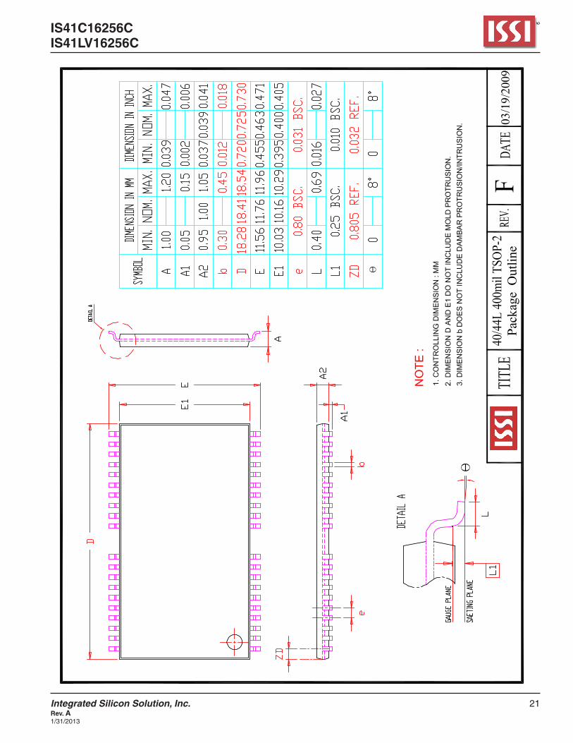
Integrated Silicon Solution, Inc. 21Rev. A1/31/2013
IS41C16256CIS41LV16256C