Embed Size (px)
Citation preview

Integrated Silicon Solution, Inc. — www.issi.com — 1-800-379-4774 1Rev. F08/25/2014
Copyright © 2014 Integrated Silicon Solution, Inc. All rights reserved. ISSI reserves the right to make changes to this specification and its products at any time without notice. ISSI assumes no liability arising out of the application or use of any information, products or services described herein. Customers are advised to obtain the lat-est version of this device specification before relying on any published information and before placing orders for products.
Integrated Silicon Solution, Inc. does not recommend the use of any of its products in life support applications where the failure or malfunction of the product can reason-ably be expected to cause failure of the life support system or to significantly affect its safety or effectiveness. Products are not authorized for use in such applications unless Integrated Silicon Solution, Inc. receives written assurance to its satisfaction, that:a.) the risk of injury or damage has been minimized;b.) the user assume all such risks; andc.) potential liability of Integrated Silicon Solution, Inc is adequately protected under the circumstances
IS62WV25616ALLIS62WV25616BLL256K x 16 LOW VOLTAGE, ULTRA LOW POWER CMOS STATIC SRAM FEATURES
• High-speedaccesstime:55ns,70ns
• CMOSlowpoweroperation
36 mW (typical) operating
9µW(typical)CMOSstandby
• TTLcompatibleinterfacelevels
• Singlepowersupply
1.65V--2.2V Vdd (IS62WV25616ALL)
2.5V--3.6V Vdd (IS62WV25616BLL)
• Fullystaticoperation:noclockorrefresh required
• Threestateoutputs
• Datacontrolforupperandlowerbytes
• Industrialtemperatureavailable
• Lead-freeavailable
DESCRIPTION
TheISSIIS62WV25616ALL/IS62WV25616BLLarehigh-speed,lowpower,4MbitSRAMsorganizedas256Kwordsby 16 bits. It is fabricated using ISSI's high-performance CMOStechnology.Thishighlyreliableprocesscoupledwithinnovative circuit design techniques, yields high-performance and low power consumption devices.
When CS1isHIGH(deselected)orwhen CS1 is LOW and both LB and UBareHIGH,thedeviceassumesastandbymode at which the power dissipation can be reduced down withCMOSinputlevels.
Easy memory expansion is provided by using Chip Enable andOutputEnableinputs.TheactiveLOWWriteEnable(WE) controls both writing and reading of the memory. A data byte allows Upper Byte (UB)andLowerByte(LB) access.
TheIS62WV25616ALL/IS62WV25616BLLarepackagedintheJEDECstandard44-PinTSOP(TYPEII) and 48-pin miniBGA(6mmx8mm).
FUNCTIONAL BLOCK DIAGRAM
AUGUST 2014
A0-A17
CS1OEWE
256K x 16MEMORY ARRAYDECODER
COLUMN I/O
CONTROLCIRCUIT
GND
VDD
I/ODATA
CIRCUIT
I/O0-I/O7Lower Byte
I/O8-I/O15Upper Byte
UBLB
2 Integrated Silicon Solution, Inc. — www.issi.com — 1-800-379-4774 Rev. F
08/25/2014
IS62WV25616ALL, IS62WV25616BLL
PIN DESCRIPTIONS
A0-A17 AddressInputs
I/O0-I/O15 DataInputs/Outputs
CS1, CS2 Chip Enable Input
OE OutputEnableInput
WE Write Enable Input
LB Lower-byteControl(I/O0-I/O7)
UB Upper-byteControl(I/O8-I/O15)
NC No Connection
Vdd Power
GND Ground
44-Pin mini TSOP (Type II)(Package Code T)
12345678910111213141516171819202122
44434241403938373635343332313029282726252423
A4A3A2A1A0CS1I/O0I/O1I/O2I/O3VDD
GNDI/O4I/O5I/O6I/O7WEA16A15A14A13A12
A5A6A7OEUBLBI/O15I/O14I/O13I/O12GNDVDD
I/O11I/O10I/O9I/O8NCA8A9A10A11A17
PIN CONFIGURATIONS48- ball mini BGA (6mm x 8mm)(Package Code B)
1 2 3 4 5 6
A
B
C
D
E
F
G
H
LB OE A0 A1 A2 NC
I/O8 UB A3 A4 CSI I/O0
I/O9 I/O10 A5 A6 I/O1 I/O2
GND I/O11 A17 A7 I/O3 VDD
VDD I/O12 NC A16 I/O4 GND
I/O14 I/O13 A14 A15 I/O5 I/O6
I/O15 NC A12 A13 WE I/O7
NC A8 A9 A10 A11 NC
44-Pin mini TSOP (Type II)2 Chip Enable Option(Package Code T2)
12345678910111213141516171819202122
44434241403938373635343332313029282726252423
A4A3A2A1A0CS1I/O0I/O1I/O2I/O3VDD
GNDI/O4I/O5I/O6I/O7WEA16A15A14A13A12
A5A6A7OEUBLBI/O15I/O14I/O13I/O12GNDVDD
I/O11I/O10I/O9I/O8CS2A8A9A10A11A17

Integrated Silicon Solution, Inc. — www.issi.com — 1-800-379-4774 3Rev. F08/25/2014
IS62WV25616ALL, IS62WV25616BLL
DC ELECTRICAL CHARACTERISTICS (OverOperatingRange) Symbol Parameter Test Conditions Vdd Min. Max. Unit
Voh OutputHIGHVoltage Ioh = -0.1 mA 1.65-2.2V 1.4 — V Ioh = -1 mA 2.5-3.6V 2.2 — V
Vol OutputLOWVoltage Iol = 0.1 mA 1.65-2.2V — 0.2 V Iol = 2.1 mA 2.5-3.6V — 0.4 V
VIh InputHIGHVoltage 1.65-2.2V 1.4 Vdd + 0.2 V 2.5-3.6V 2.2 Vdd + 0.3 V
VIl(1) InputLOWVoltage 1.65-2.2V –0.2 0.4 V 2.5-3.6V –0.2 0.8 V
IlI InputLeakage GND≤ VIn ≤ Vdd –1 1 µA
Ilo OutputLeakage GND≤ Vout ≤ Vdd, OutputsDisabled –1 1 µANotes: 1. VIl (min.) = –1.0V for pulse width less than 10 ns.
OPERATING RANGE (Vdd) Range Ambient Temperature IS62WV25616ALL IS62WV25616BLL
Commercial 0°Cto+70°C 1.65V-2.2V 2.5V-3.6V
Industrial –40°C to +85°C 1.65V - 2.2V 2.5V-3.6V
ABSOLUTE MAXIMUM RATINGS(1)
Symbol Parameter Value Unit
Vterm TerminalVoltagewithRespecttoGND –0.2toVdd+0.3 V
Vdd VddRelatedtoGND –0.2toVdd+0.3 V
tstg StorageTemperature –65to+150 °C
Pt PowerDissipation 1.0 WNote:1.StressgreaterthanthoselistedunderABSOLUTEMAXIMUMRATINGSmaycausepermanentdamagetothedevice.This
is a stress rating only and functional operation of the device at these or any other conditions above those indicated in the op-erational sections of this specification is not implied. Exposure to absolute maximum rating conditions for extended periods may affect reliability.
TRUTH TABLE I/O PIN Mode WE CS1 OE LB UB I/O0-I/O7 I/O8-I/O15 Vdd Current
NotSelected X H X X X High-Z High-Z Isb1, Isb2
X X X H H High-Z High-Z Isb1, Isb2
OutputDisabled H L H L X High-Z High-Z Icc H L H X L High-Z High-Z Icc
Read H L L L H dout High-Z Icc H L L H L High-Z dout h l l l l dout dout
Write L L X L H dIn High-Z Icc L L X H L High-Z dIn l l X l l dIn dIn
4 Integrated Silicon Solution, Inc. — www.issi.com — 1-800-379-4774 Rev. F
08/25/2014
IS62WV25616ALL, IS62WV25616BLL
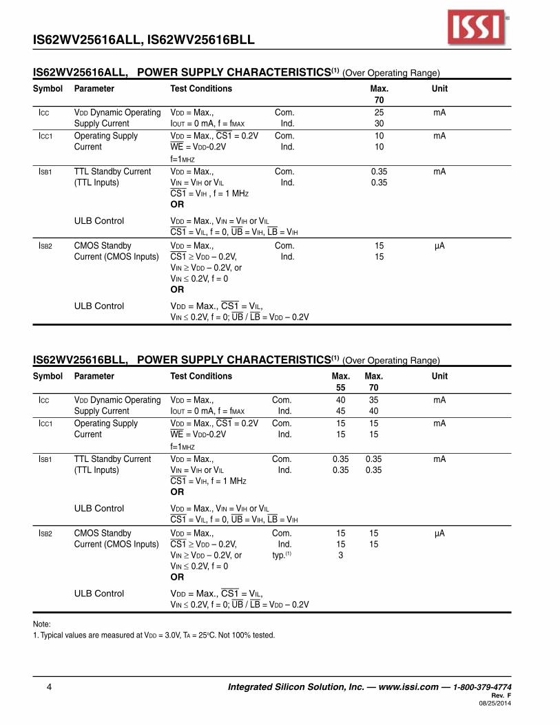
IS62WV25616ALL, POWER SUPPLY CHARACTERISTICS(1) (OverOperatingRange)
Symbol Parameter Test Conditions Max. Unit 70 Icc Vdd DynamicOperating Vdd = Max., Com. 25 mA Supply Current Iout = 0 mA, f = fmaX Ind. 30 Icc1 OperatingSupply Vdd = Max.,CS1 = 0.2V Com. 10 mA Current WE = Vdd-0.2V Ind. 10 f=1mhz
Isb1 TTLStandbyCurrent Vdd = Max., Com. 0.35 mA (TTLInputs) VIn = VIh or VIl Ind. 0.35 CS1 = VIh ,f=1MHz OR
ULBControl Vdd=Max.,VIn = VIh or VIl
CS1 = VIl, f = 0, UB = VIh, LB = VIh
Isb2 CMOSStandby Vdd = Max., Com. 15 µA Current(CMOSInputs) CS1 ≥ Vdd – 0.2V, Ind. 15 VIn ≥ Vdd – 0.2V, or VIn ≤ 0.2V, f = 0 OR
ULBControl Vdd=Max.,CS1 = VIl, VIn ≤ 0.2V, f = 0; UB / LB = Vdd – 0.2V
IS62WV25616BLL, POWER SUPPLY CHARACTERISTICS(1) (OverOperatingRange)
Symbol Parameter Test Conditions Max. Max. Unit 55 70 Icc VddDynamicOperating Vdd = Max., Com. 40 35 mA Supply Current Iout = 0 mA, f = fmaX Ind. 45 40 Icc1 OperatingSupply Vdd = Max.,CS1 = 0.2V Com. 15 15 mA Current WE = Vdd-0.2V Ind. 15 15 f=1mhz
Isb1 TTLStandbyCurrent Vdd = Max., Com. 0.35 0.35 mA (TTLInputs) VIn = VIh or VIl Ind. 0.35 0.35 CS1 = VIh,f=1MHz OR
ULBControl Vdd=Max.,VIn = VIh or VIl
CS1 = VIl, f = 0, UB = VIh, LB = VIh
Isb2 CMOSStandby Vdd = Max., Com. 15 15 µA Current(CMOSInputs) CS1 ≥ Vdd – 0.2V, Ind. 15 15 VIn ≥ Vdd – 0.2V, or typ.(1) 3 VIn ≤ 0.2V, f = 0 OR
ULBControl Vdd=Max.,CS1 = VIl, VIn ≤ 0.2V, f = 0; UB / LB = Vdd – 0.2V Note: 1.TypicalvaluesaremeasuredatVdd=3.0V,Ta = 25oC. Not 100% tested.

Integrated Silicon Solution, Inc. — www.issi.com — 1-800-379-4774 5Rev. F08/25/2014
IS62WV25616ALL, IS62WV25616BLL
AC TEST CONDITIONS
IS62WV25616ALL IS62WV25616BLL Parameter (Unit) (Unit)
InputPulseLevel 0.4VtoVdd-0.2V 0.4V to Vdd-0.3V
InputRiseandFallTimes 5ns 5ns
InputandOutputTiming Vref Vref andReferenceLevel
OutputLoad SeeFigures1and2 SeeFigures1and2
AC TEST LOADS
Figure 1 Figure 2
IS62WV25616ALL IS62WV25616BLL
1.65V-2.2V 2.5V - 3.6V
R1(Ω) 3070 3070
R2(Ω) 3150 3150
VRef 0.9V 1.5V
Vtm 1.8V 2.8V
R1
5 pFIncluding
jig andscope
R2
OUTPUT
VTMR1
30 pFIncluding
jig andscope
R2
OUTPUT
VTM
CAPACITANCE(1)
Symbol Parameter Conditions Max. Unit
cIn Input Capacitance VIn = 0V 8 pF
cout Input/OutputCapacitance Vout = 0V 10 pFNote:1.Testedinitiallyandafteranydesignorprocesschangesthatmayaffecttheseparameters.

6 Integrated Silicon Solution, Inc. — www.issi.com — 1-800-379-4774 Rev. F
08/25/2014
IS62WV25616ALL, IS62WV25616BLL
READ CYCLE SWITCHING CHARACTERISTICS(1) (OverOperatingRange)
55 ns 70 ns Symbol Parameter Min. Max. Min. Max. Unit
trc ReadCycleTime 55 — 70 — ns
taa AddressAccessTime — 55 — 70 ns
toha OutputHoldTime 10 — 10 — ns
tacs1 CS1AccessTime — 55 — 70 ns
tdoe OEAccessTime — 25 — 35 ns
thzoe(2) OEtoHigh-ZOutput — 20 — 25 ns
tlzoe(2) OEtoLow-ZOutput 5 — 5 — ns
thzcs1 CS1toHigh-ZOutput 0 20 0 25 ns
tlzcs1 CS1toLow-ZOutput 10 — 10 — ns
tba LB, UBAccessTime — 55 — 70 ns
thzb LB, UBtoHigh-ZOutput 0 20 0 25 ns
tlzb LB, UBtoLow-ZOutput 0 — 0 — nsNotes: 1. Testconditionsassumesignaltransitiontimesof5nsorless,timingreferencelevelsof0.9V/1.5V,inputpulselevelsof0.4to
Vdd-0.2V/Vdd-0.3VandoutputloadingspecifiedinFigure1.2. TestedwiththeloadinFigure2.Transitionismeasured±500mVfromsteady-statevoltage.Not100%tested.
Integrated Silicon Solution, Inc. — www.issi.com — 1-800-379-4774 7Rev. F08/25/2014
IS62WV25616ALL, IS62WV25616BLL
DATA VALIDPREVIOUS DATA VALID
tAA
tOHAtOHA
tRC
DOUT
ADDRESS
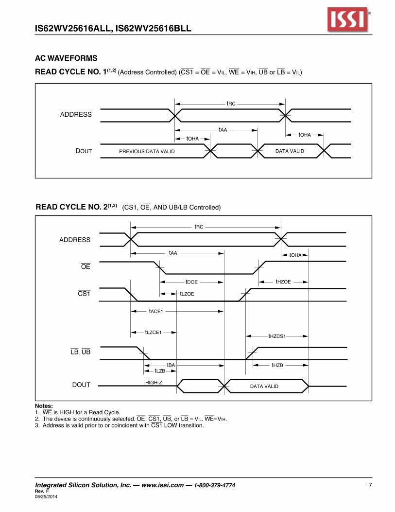
AC WAVEFORMS
READ CYCLE NO. 1(1,2) (Address Controlled) (CS1 = OE = VIl, WE = VIh, UB or LB = VIl)
tRC
tOHAtAA
tDOE
tLZOE
tACE1
tLZCE1
tHZOE
HIGH-ZDATA VALID
tHZCS1
ADDRESS
OE
CS1
DOUT
LB, UB
tHZBtBAtLZB
READ CYCLE NO. 2(1,3) (CS1, OE,ANDUB/LB Controlled)
Notes: 1. WEisHIGHforaReadCycle.2. Thedeviceiscontinuouslyselected.OE, CS1, UB, or LB = VIl. WE=VIh.3. Address is valid prior to or coincident with CS1LOWtransition.

8 Integrated Silicon Solution, Inc. — www.issi.com — 1-800-379-4774 Rev. F
08/25/2014
IS62WV25616ALL, IS62WV25616BLL
WRITE CYCLE SWITCHING CHARACTERISTICS(1,2)(OverOperatingRange)
55 ns 70 ns Symbol Parameter Min. Max. Min. Max. Unit twc WriteCycleTime 55 — 70 — ns
tscs1 CS1 to Write End 45 — 60 — ns
taw AddressSetupTimetoWriteEnd 45 — 60 — ns
tha AddressHoldfromWriteEnd 0 — 0 — ns
tsa AddressSetupTime 0 — 0 — ns
tPwb LB, UB Valid to End of Write 45 — 60 — ns
tPwe WE Pulse Width 40 — 50 — ns
tsd DataSetuptoWriteEnd 25 — 30 — ns
thd DataHoldfromWriteEnd 0 — 0 — ns
thzwe(3) WELOWtoHigh-ZOutput — 20 — 20 ns
tlzwe(3) WEHIGHtoLow-ZOutput 5 — 5 — ns
Notes:
1. Testconditionsassumesignaltransitiontimesof5nsorless,timingreferencelevelsof0.9V/1.5V,inputpulselevelsof0.4VtoVdd-0.2V/Vdd-0.3VandoutputloadingspecifiedinFigure1.
2. TheinternalwritetimeisdefinedbytheoverlapofCS1LOWandUB or LB, and WELOW.AllsignalsmustbeinvalidstatestoinitiateaWrite,butanyonecan go inactive to terminatetheWrite.TheDataInputSetupandHoldtimingarereferencedtotherisingorfallingedgeofthesignalthatterminatesthewrite.
3. TestedwiththeloadinFigure2.Transitionismeasured±500mVfromsteady-statevoltage.Not100%tested.

Integrated Silicon Solution, Inc. — www.issi.com — 1-800-379-4774 9Rev. F08/25/2014
IS62WV25616ALL, IS62WV25616BLL
WRITE CYCLE NO. 2 (WE Controlled: OEisHIGHDuringWriteCycle)
DATA-IN VALID
DATA UNDEFINED
tWC
tSCS1
tAW
tHA
t PWE
tHZWE
HIGH-Z
tLZWEtSA
tSD tHD
ADDRESS
OE
CS1
WE
LB, UB
DOUT
DIN
Notes: 1. WRITEisaninternallygeneratedsignalassertedduringanoverlapoftheLOWstatesontheCS1 and WE inputs and at
least one of the LB and UBinputsbeingintheLOWstate.2. WRITE=(CS1) [ (LB) = (UB) ] (WE).
AC WAVEFORMS
WRITE CYCLE NO. 1(1,2) (CS1 Controlled, OE=HIGHorLOW)
DATA-IN VALID
DATA UNDEFINED
tWC
tSCS1
tAW
tHA
tPWE
tHZWE
HIGH-Z
tLZWEtSA
tSD tHD
ADDRESS
CS1
WE
DOUT
DIN
LB, UBtPWB

10 Integrated Silicon Solution, Inc. — www.issi.com — 1-800-379-4774 Rev. F
08/25/2014
IS62WV25616ALL, IS62WV25616BLL
WRITE CYCLE NO. 4 (UB/LB Controlled)
DATA UNDEFINED
t WC
ADDRESS 1 ADDRESS 2
t WC
HIGH-Z
t PBW
WORD 1
LOW
WORD 2
t HD
t SA
t HZWE
ADDRESS
CS1
UB, LB
WE
DOUT
DIN
OE
DATAINVALID
t LZWE
t SD
t PBW
DATAINVALID
t SDt HD
t SA
t HA t HA
UB_CSWR4.eps
WRITE CYCLE NO. 3 (WE Controlled: OEisLOWDuringWriteCycle)
DATA-IN VALID
DATA UNDEFINED
tWC
tSCS1
tAW
tHA
tPWE
tHZWE
HIGH-Z
tLZWEtSA
tSD tHD
ADDRESS
OE
CS1
WE
LB, UB
DOUT
DIN

Integrated Silicon Solution, Inc. — www.issi.com — 1-800-379-4774 11Rev. F08/25/2014
IS62WV25616ALL, IS62WV25616BLL
DATA RETENTION WAVEFORM (CS1 Controlled)
VDD
CS1 ≥ VDD - 0.2V
tSDR tRDR
VDR
CS1GND
Data Retention Mode
DATA RETENTION SWITCHING CHARACTERISTICS Symbol Parameter Test Condition Min. Max. Unit Vdr VddforDataRetention SeeDataRetentionWaveform 1.2 3.6 V Idr DataRetentionCurrent Vdd = 1.2V, CS1 ≥ Vdd – 0.2V — 15 µA tsdr DataRetentionSetupTime SeeDataRetentionWaveform 0 — ns trdr RecoveryTime SeeDataRetentionWaveform trc — ns

12 Integrated Silicon Solution, Inc. — www.issi.com — 1-800-379-4774 Rev. F
08/25/2014
IS62WV25616ALL, IS62WV25616BLL
IS62WV25616BLL (2.5V - 3.6V)
Commercial Range: 0°C to +70°C Speed (ns) Order Part No. Package
55 IS62WV25616BLL-55T TSOP
70 IS62WV25616BLL-70T TSOP
Industrial Range: –40°C to +85°C Speed (ns) Order Part No. Package
55 IS62WV25616BLL-55TI TSOP
55 IS62WV25616BLL-55TLI TSOP,Lead-free
55 IS62WV25616BLL-55T2LI TSOP,Lead-free,2CSOption
55 IS62WV25616BLL-55BI miniBGA(6mmx8mm)
55 IS62WV25616BLL-55BLI miniBGA(6mmx8mm),Lead-free
ORDERING INFORMATION
IS62WV25616ALL (1.65V-2.2V)
Commercial Range: 0°C to +70°C Speed (ns) Order Part No. Package
70 IS62WV25616ALL-70T TSOP
Industrial Range: –40°C to +85°C Speed (ns) Order Part No. Package
70 IS62WV25616ALL-70TI TSOP
70 IS62WV25616ALL-70BI miniBGA(6mmx8mm)
70 IS62WV25616ALL-70BLI miniBGA(6mmx8mm),Lead-free
Integrated Silicon Solution, Inc. — www.issi.com — 1-800-379-4774 13Rev. F08/25/2014
IS62WV25616ALL, IS62WV25616BLL
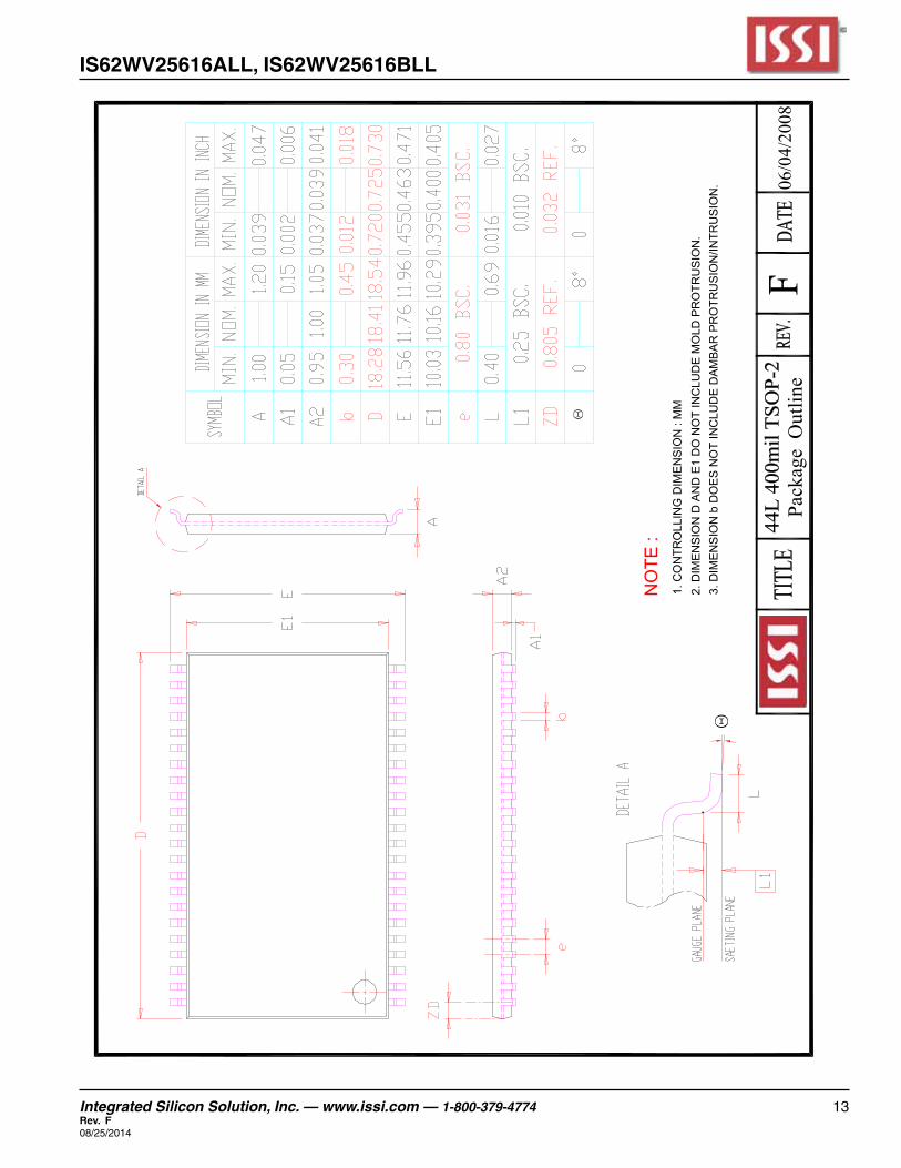
2. D
IMEN
SIO
N D
AN
D E
1 D
O N
OT
INC
LUD
E M
OLD
PR
OTR
USI
ON
.3.
DIM
EN
SIO
N b
DO
ES
NO
T IN
CLU
DE
DA
MB
AR
PR
OTR
US
ION
/INTR
US
ION
.
1. C
ON
TRO
LLIN
G D
IME
NS
ION
: M
M
NO
TE :
Θ
Θ
06/0
4/20
08Pa
ckag
e O
utlin
e

14 Integrated Silicon Solution, Inc. — www.issi.com — 1-800-379-4774 Rev. F
08/25/2014
IS62WV25616ALL, IS62WV25616BLL
2. R
efer
ence
doc
umen
t : J
EDEC
MO
-207
1. C
ON
TRO
LLIN
G D
IMEN
SIO
N :
MM
.
NO
TE :
08/1
2/20
08Pa
ckag
e O
utlin
e
![Untitled Document [] · to IC Unless otherwise indicated, all limits are specified for VDD = +2.7V to +5.5V, VSS = GND, TA = 25 °C, VCM = VDD/2, RL = 100kΩ to VDD/2, and VOUT ~](https://img.pdfslide.us/doc/110x75/5e7405a09fd2db4c0a486c73/untitled-document-to-ic-unless-otherwise-indicated-all-limits-are-specified.jpg)