Embed Size (px)
Citation preview
Arm® Cortex®-M55 ProcessorRevision: r0p2
Technical Reference Manual
Copyright © 2019, 2020 Arm Limited or its affiliates. All rights reserved.101051_0002_02_en
Arm® Cortex®-M55 ProcessorTechnical Reference ManualCopyright © 2019, 2020 Arm Limited or its affiliates. All rights reserved.
Release Information
Document History
Issue Date Confidentiality Change
0000-02 07 June 2019 Confidential First beta release for r0p0
0000-04 20 December 2019 Confidential First limited access release for r0p0
0001-05 31 March 2020 Non-Confidential First early access release for r0p1
0002-01 16 July 2020 Non-Confidential First release for r0p2
0002-02 30 October 2020 Non-Confidential Second release for r0p2
Non-Confidential Proprietary Notice
This document is protected by copyright and other related rights and the practice or implementation of the information contained inthis document may be protected by one or more patents or pending patent applications. No part of this document may bereproduced in any form by any means without the express prior written permission of Arm. No license, express or implied, byestoppel or otherwise to any intellectual property rights is granted by this document unless specifically stated.
Your access to the information in this document is conditional upon your acceptance that you will not use or permit others to usethe information for the purposes of determining whether implementations infringe any third party patents.
THIS DOCUMENT IS PROVIDED “AS IS”. ARM PROVIDES NO REPRESENTATIONS AND NO WARRANTIES,EXPRESS, IMPLIED OR STATUTORY, INCLUDING, WITHOUT LIMITATION, THE IMPLIED WARRANTIES OFMERCHANTABILITY, SATISFACTORY QUALITY, NON-INFRINGEMENT OR FITNESS FOR A PARTICULAR PURPOSEWITH RESPECT TO THE DOCUMENT. For the avoidance of doubt, Arm makes no representation with respect to, and hasundertaken no analysis to identify or understand the scope and content of, third party patents, copyrights, trade secrets, or otherrights.
This document may include technical inaccuracies or typographical errors.
TO THE EXTENT NOT PROHIBITED BY LAW, IN NO EVENT WILL ARM BE LIABLE FOR ANY DAMAGES,INCLUDING WITHOUT LIMITATION ANY DIRECT, INDIRECT, SPECIAL, INCIDENTAL, PUNITIVE, ORCONSEQUENTIAL DAMAGES, HOWEVER CAUSED AND REGARDLESS OF THE THEORY OF LIABILITY, ARISINGOUT OF ANY USE OF THIS DOCUMENT, EVEN IF ARM HAS BEEN ADVISED OF THE POSSIBILITY OF SUCHDAMAGES.
This document consists solely of commercial items. You shall be responsible for ensuring that any use, duplication or disclosure ofthis document complies fully with any relevant export laws and regulations to assure that this document or any portion thereof isnot exported, directly or indirectly, in violation of such export laws. Use of the word “partner” in reference to Arm’s customers isnot intended to create or refer to any partnership relationship with any other company. Arm may make changes to this document atany time and without notice.
If any of the provisions contained in these terms conflict with any of the provisions of any click through or signed writtenagreement covering this document with Arm, then the click through or signed written agreement prevails over and supersedes theconflicting provisions of these terms. This document may be translated into other languages for convenience, and you agree that ifthere is any conflict between the English version of this document and any translation, the terms of the English version of theAgreement shall prevail.
The Arm corporate logo and words marked with ® or ™ are registered trademarks or trademarks of Arm Limited (or itssubsidiaries) in the US and/or elsewhere. All rights reserved. Other brands and names mentioned in this document may be thetrademarks of their respective owners. Please follow Arm’s trademark usage guidelines at http://www.arm.com/company/policies/trademarks.
Copyright © 2019, 2020 Arm Limited (or its affiliates). All rights reserved.
Arm Limited. Company 02557590 registered in England.
Arm® Cortex®-M55 Processor
101051_0002_02_en Copyright © 2019, 2020 Arm Limited or its affiliates. All rightsreserved.
2
Non-Confidential
110 Fulbourn Road, Cambridge, England CB1 9NJ.
(LES-PRE-20349)
Confidentiality Status
This document is Non-Confidential. The right to use, copy and disclose this document may be subject to license restrictions inaccordance with the terms of the agreement entered into by Arm and the party that Arm delivered this document to.
Unrestricted Access is an Arm internal classification.
Product Status
The information in this document is Final, that is for a developed product.
Web Address
developer.arm.com
Arm® Cortex®-M55 Processor
101051_0002_02_en Copyright © 2019, 2020 Arm Limited or its affiliates. All rightsreserved.
3
Non-Confidential
ContentsArm® Cortex®-M55 Processor Technical ReferenceManual
PrefaceAbout this book ..................................................... ..................................................... 11Feedback .................................................................................................................... 15
Chapter 1 Introduction1.1 Cortex®-M55 processor overview ...................................... ...................................... 1-171.2 Cortex®-M55 features ............................................... ............................................... 1-181.3 Supported standards and specifications .................................................................. 1-211.4 Design tasks ............................................................................................................ 1-231.5 Documentation .................................................... .................................................... 1-241.6 Product revisions .................................................. .................................................. 1-25
Chapter 2 Technical overview2.1 Cortex®-M55 processor components ................................... ................................... 2-272.2 Interfaces ........................................................ ........................................................ 2-342.3 Security .................................................................................................................... 2-362.4 Reliability ........................................................ ........................................................ 2-372.5 Power intent ...................................................... ...................................................... 2-382.6 Cortex®-M55 implementation options ................................... ................................... 2-39
Chapter 3 Programmers model3.1 Security states, operation, and execution modes .................................................... 3-43
101051_0002_02_en Copyright © 2019, 2020 Arm Limited or its affiliates. All rightsreserved.
4
Non-Confidential
3.2 Instruction set summary ............................................. ............................................. 3-443.3 Exclusive monitor .................................................. .................................................. 3-453.4 Cortex®-M55 processor core registers summary .......................... .......................... 3-463.5 Architectural registers .............................................................................................. 3-483.6 Exceptions ....................................................... ....................................................... 3-49
Chapter 4 System registers4.1 System control register summary ............................................................................ 4-514.2 Identification register summary ................................................................................ 4-554.3 AFSR, Auxiliary Fault Status Register .................................. .................................. 4-594.4 CPUID, CPUID Base Register ........................................ ........................................ 4-614.5 Cache identification register summary .................................. .................................. 4-624.6 REVIDR, Revision ID Register ........................................ ........................................ 4-664.7 Implementation control register summary ............................... ............................... 4-674.8 ACTLR, Auxiliary Control Register ..................................... ..................................... 4-684.9 ICTR, Interrupt Controller Type Register ................................ ................................ 4-714.10 IMPLEMENTATION DEFINED registers summary .................................................. 4-724.11 Direct cache access registers .................................................................................. 4-754.12 Error bank registers ................................................ ................................................ 4-814.13 MSCR, Memory System Control Register ............................... ............................... 4-874.14 PAHBCR, P-AHB Control Register .......................................................................... 4-904.15 PFCR, Prefetcher Control Register .................................... .................................... 4-914.16 Power mode control registers .................................................................................. 4-924.17 Processor configuration information registers ............................ ............................ 4-954.18 ID_PFR0, Processor Feature Register 0 ............................... ............................... 4-1004.19 ITCMCR and DTCMCR, TCM Control Registers ......................... ......................... 4-1014.20 TCM security gate registers ......................................... ......................................... 4-1034.21 EWIC interrupt status access registers ................................ ................................ 4-108
Chapter 5 Initialization5.1 Initialization overview .............................................. .............................................. 5-1125.2 Initializing and reprogramming the MPU ................................................................ 5-1135.3 Initializing the EPU ................................................ ................................................ 5-1145.4 Programming the SAU ............................................. ............................................. 5-1155.5 Initializing the instruction and data cache .............................................................. 5-1165.6 Enabling the branch cache .......................................... .......................................... 5-1185.7 Enabling and preloading the TCM .................................... .................................... 5-1195.8 Enabling and locking the TCM security gates ........................... ........................... 5-1205.9 Enabling the P-AHB interface ................................................................................ 5-121
Chapter 6 Power management6.1 Power domains ...................................................................................................... 6-1236.2 Power states .......................................................................................................... 6-1256.3 Power and operating mode transitions .................................................................. 6-1266.4 Core P-Channel and power mode selection .......................................................... 6-1306.5 COREPACTIVE and required power mode ............................. ............................. 6-1326.6 PDCORE low-power requirements ........................................................................ 6-1356.7 PDEPU low-power requirements ..................................... ..................................... 6-1366.8 PDRAMS powerdown requirements ...................................................................... 6-1376.9 Warm reset power mode ........................................... ........................................... 6-138
101051_0002_02_en Copyright © 2019, 2020 Arm Limited or its affiliates. All rightsreserved.
5
Non-Confidential
6.10 Debug Q-Channel and PDDEBUG power domain ........................ ........................ 6-1406.11 Q-Channel clock control ........................................... ........................................... 6-1416.12 PWRDBGWAKEQACTIVE ......................................... ......................................... 6-142
Chapter 7 Memory model7.1 Memory map .......................................................................................................... 7-1447.2 Memory types ........................................................................................................ 7-1467.3 Private Peripheral Bus ............................................. ............................................. 7-1487.4 Unaligned accesses ............................................... ............................................... 7-1507.5 Access privilege level for Device and Normal memory .................... .................... 7-1527.6 Memory ordering and barriers ....................................... ....................................... 7-1537.7 Execute Only Memory ............................................. ............................................. 7-154
Chapter 8 Memory Authentication8.1 MAU features .................................................... .................................................... 8-1568.2 Security Attribution Unit ............................................ ............................................ 8-1578.3 Memory Protection Unit ............................................ ............................................ 8-1598.4 Implementation Defined Attribution Unit ................................................................ 8-1618.5 Memory regions not controlled by SAU and IDAU ........................ ........................ 8-1628.6 Security attribution signals .......................................... .......................................... 8-1638.7 TCM Gate Units .................................................. .................................................. 8-1648.8 TCM and P-AHB security access control ............................... ............................... 8-165
Chapter 9 Memory system9.1 Memory system features ........................................... ........................................... 9-1719.2 Memory system faults ............................................................................................ 9-1739.3 Memory system behavior ........................................... ........................................... 9-1759.4 Master-AXI interface .............................................................................................. 9-1799.5 Peripheral AHB interface ........................................... ........................................... 9-1859.6 S-AHB interface .................................................. .................................................. 9-1889.7 EPPB interface ................................................... ................................................... 9-1919.8 TCM interfaces ................................................... ................................................... 9-1929.9 Instruction and data cache .......................................... .......................................... 9-1969.10 Store buffer ............................................................................................................ 9-2049.11 Internal local exclusive access monitor ................................ ................................ 9-2069.12 M-AXI and P-AHB interaction with the global exclusive monitor ............. ............. 9-2079.13 MBIST .................................................................................................................... 9-208
Chapter 10 Reliability, Availability, and Serviceability Extension support10.1 Cortex®-M55 processor implementation of RAS .................................................. 10-21010.2 ECC memory protection behavior ................................... ................................... 10-21210.3 Interface protection behavior ....................................... ....................................... 10-21910.4 RAS memory barriers .......................................................................................... 10-22110.5 RAS Extension registers ...................................................................................... 10-222
Chapter 11 Nested Vectored Interrupt Controller11.1 NVIC features ................................................... ................................................... 11-23211.2 Registers associated with interrupt control and behavior .................. .................. 11-23311.3 NVIC register summary ........................................... ........................................... 11-23411.4 Software Interrupt Generation register summary ........................ ........................ 11-23511.5 SysTick Timer register summary .................................... .................................... 11-236
101051_0002_02_en Copyright © 2019, 2020 Arm Limited or its affiliates. All rightsreserved.
6
Non-Confidential
Chapter 12 External coprocessors12.1 External coprocessors features ..................................... ..................................... 12-23812.2 Operation ...................................................... ...................................................... 12-23912.3 Data transfer rates ............................................... ............................................... 12-24012.4 Coprocessor instruction restrictions .................................. .................................. 12-24112.5 Debug access to coprocessor registers usage constraints ................ ................ 12-24212.6 Exceptions and context switch ...................................... ...................................... 12-24312.7 Response to coprocessor errors .................................... .................................... 12-24412.8 Hazard between load and store instructions followed by coprocessor transactions ....
.............................................................................................................................. 12-245
Chapter 13 Floating-point and MVE support13.1 Floating-point and MVE operation ................................... ................................... 13-24713.2 Floating-point and MVE register summary ............................. ............................. 13-24913.3 FPDSCR and FPSCR register reset values ............................ ............................ 13-25013.4 Powering down the EPU ...................................................................................... 13-251
Chapter 14 Debug14.1 Debug functionality .............................................................................................. 14-25314.2 D-AHB interface ................................................. ................................................. 14-259
Chapter 15 Performance Monitoring Unit Extension15.1 PMU features ................................................... ................................................... 15-26615.2 PMU events .................................................... .................................................... 15-26715.3 PMU register summary ........................................................................................ 15-272
Chapter 16 Instrumentation Trace Macrocell16.1 ITM features .................................................... .................................................... 16-27516.2 ITM register summary ............................................ ............................................ 16-27716.3 ITM_TPR, ITM Trace Privilege Register .............................................................. 16-27916.4 ITM_ITCTRL, ITM Integration Mode Control Register .................... .................... 16-28016.5 ITM_ITWRITE, Integration Write Register ............................. ............................. 16-28116.6 ITM_ITREAD, Integration Read Register .............................. .............................. 16-282
Chapter 17 Data Watchpoint and Trace17.1 DWT features ................................................... ................................................... 17-28417.2 DWT debug access control ........................................ ........................................ 17-28617.3 DWT comparators ............................................... ............................................... 17-28817.4 Cycle counter and profiling counters ................................. ................................. 17-28917.5 DWT register summary ........................................................................................ 17-290
Chapter 18 Cross Trigger Interface18.1 CTI features .................................................... .................................................... 18-29418.2 CTI register summary .......................................................................................... 18-29618.3 CTI_CONTROL, CTI Control Register ................................ ................................ 18-29818.4 CTI_INACK, CTI Interrupt Acknowledge Register ....................... ....................... 18-29918.5 CTI_APPSET, CTI Application Channel Set Register .................... .................... 18-30018.6 CTI_APPCLR, CTI Application Channel Clear Register ...................................... 18-30118.7 CTI_APPPULSE, CTI Application Channel Pulse Register ................ ................ 18-30218.8 CTI_INEN<n>, n=0-5, CTI Trigger <n> to Channel Enable Register ......... ......... 18-30318.9 CTI_OUTEN<n>, n=0-7, CTI Channel <n> to Trigger Enable Register ....... ....... 18-304
101051_0002_02_en Copyright © 2019, 2020 Arm Limited or its affiliates. All rightsreserved.
7
Non-Confidential
18.10 CTI_TRIGINSTATUS, CTI Trigger Input Status Register .................. .................. 18-30618.11 CTI_TRIGOUTSTATUS, CTI Trigger Output Status Register .............................. 18-30718.12 CTI_CHINSTATUS, CTI Channel Input Status Register ...................................... 18-30818.13 CTI_CHOUTSTATUS, CTI Channel Output Status Register ............... ............... 18-30918.14 CTI_CHANNELGATE, CTI Channel Gate Register ...................... ...................... 18-31018.15 CTI_ITCHOUT, Integration Test Channel Output Register .................................. 18-31118.16 CTI_ITTRIGOUT, Integration Test Trigger Output Register ................ ................ 18-31218.17 CTI_ITCHIN, Integration Test Channel Input Register .................... .................... 18-31418.18 CTI_ITTRIGIN, Integration Test Trigger Input Register ................... ................... 18-31518.19 CTI_ITCONTROL, Integration Mode Control Register ........................................ 18-31618.20 CTI_DEVARCH, Device Architecture Register .................................................... 18-31718.21 CTI_DEVID, Device Configuration Register ........................................................ 18-31818.22 CTI_DEVTYPE, Device Type Identifier Register ........................ ........................ 18-31918.23 CTI_PIDR4, Peripheral Identification Register 4 ........................ ........................ 18-32018.24 CTI_PIDR5, Peripheral Identification Register 5 ........................ ........................ 18-32118.25 CTI_PIDR6, Peripheral Identification Register 6 ........................ ........................ 18-32218.26 CTI_PIDR7, Peripheral Identification Register 7 ........................ ........................ 18-32318.27 CTI_PIDR0, Peripheral Identification Register 0 ........................ ........................ 18-32418.28 CTI_PIDR1, Peripheral Identification Register 1 ........................ ........................ 18-32518.29 CTI_PIDR2, Peripheral Identification Register 2 ........................ ........................ 18-32618.30 CTI_PIDR3, Peripheral Identification Register 3 ........................ ........................ 18-32718.31 CTI_ CIDR0, Component Identification Register 0 .............................................. 18-32818.32 CTI_ CIDR1, Component Identification Register 1 .............................................. 18-32918.33 CTI_ CIDR2, Component Identification Register 2 .............................................. 18-33018.34 CTI_ CIDR3, Component Identification Register 3 .............................................. 18-331
Chapter 19 Breakpoint Unit19.1 BPU features ................................................... ................................................... 19-33319.2 BPU register summary ............................................ ............................................ 19-334
Appendix A External Wakeup Interrupt ControllerA.1 EWIC features .............................................. .............................................. Appx-A-337A.2 EWIC register summary ....................................... ....................................... Appx-A-338
Appendix B Trace Port Interface UnitB.1 TPIU features ............................................... ............................................... Appx-B-350B.2 TPIU register summary ................................................................................ Appx-B-353
Appendix C Signal descriptionsC.1 Clock and clock enable signals ................................. ................................. Appx-C-377C.2 Reset signals ............................................... ............................................... Appx-C-378C.3 Static configuration signals .......................................................................... Appx-C-379C.4 Reset configuration signals .................................... .................................... Appx-C-381C.5 Cache initialization signal ...................................... ...................................... Appx-C-382C.6 Instruction execution control signals ............................................................ Appx-C-383C.7 Instruction Tightly Coupled Memory interface signals ................ ................ Appx-C-384C.8 Data Tightly Coupled Memory interface signals .......................................... Appx-C-386C.9 M-AXI interface signals ................................................................................ Appx-C-388C.10 S-AHB interface signals ....................................... ....................................... Appx-C-392C.11 P-AHB interface signals ....................................... ....................................... Appx-C-394C.12 D-AHB interface signals ....................................... ....................................... Appx-C-396
101051_0002_02_en Copyright © 2019, 2020 Arm Limited or its affiliates. All rightsreserved.
8
Non-Confidential
C.13 EPPB interface signals ................................................................................ Appx-C-398C.14 External coprocessor interface signals ........................................................ Appx-C-399C.15 Debug interface signals ....................................... ....................................... Appx-C-400C.16 P-Channel and Q-Channel power control signals ................... ................... Appx-C-401C.17 Q-Channel clock control signals .................................................................. Appx-C-402C.18 Power compatibility control signals .............................................................. Appx-C-403C.19 ITM interface signals ......................................... ......................................... Appx-C-404C.20 ETM interface signals .................................................................................. Appx-C-405C.21 Trace synchronization and trigger signals ......................... ......................... Appx-C-406C.22 CTI interface signals .................................................................................... Appx-C-407C.23 Interrupt signals ............................................. ............................................. Appx-C-408C.24 WIC interface signals ......................................... ......................................... Appx-C-409C.25 Event signals ............................................... ............................................... Appx-C-411C.26 IDAU interface signals ........................................ ........................................ Appx-C-412C.27 Miscellaneous signals .................................................................................. Appx-C-413C.28 Error interface signals .................................................................................. Appx-C-417C.29 Floating-point exception signals ................................. ................................. Appx-C-418C.30 Test interface signals ......................................... ......................................... Appx-C-419C.31 Reserved signals ............................................ ............................................ Appx-C-420
Appendix D UNPREDICTABLE BehaviorsD.1 Use of instructions defined in architecture variants .................. .................. Appx-D-422D.2 Use of Program Counter - R15 encoding .......................... .......................... Appx-D-423D.3 Use of Stack Pointer - as a general-purpose register R13 ............ ............ Appx-D-424D.4 Register list in load and store multiple instructions ...................................... Appx-D-425D.5 Exception-continuable instructions .............................................................. Appx-D-426D.6 Stack limit checking .......................................... .......................................... Appx-D-427D.7 UNPREDICTABLE instructions within an IT block ................... ................... Appx-D-428D.8 Memory access and address space ............................................................ Appx-D-429D.9 MPU programming ........................................... ........................................... Appx-D-430D.10 Miscellaneous UNPREDICTABLE instruction behavior ............... ............... Appx-D-431
Appendix E RevisionsE.1 Revisions .................................................. .................................................. Appx-E-433
101051_0002_02_en Copyright © 2019, 2020 Arm Limited or its affiliates. All rightsreserved.
9
Non-Confidential
Preface
This preface introduces the Arm® Cortex®-M55 Processor Technical Reference Manual.
It contains the following:• About this book on page 11.• Feedback on page 15.
101051_0002_02_en Copyright © 2019, 2020 Arm Limited or its affiliates. All rightsreserved.
10
Non-Confidential
About this bookThis manual is for the Cortex®-M55 processor. It provides reference information and containsprogramming details for registers. It also describes the memory system, the interrupts, the debugfeatures, and other key features of the processor.
Product revision status
The rxpy identifier indicates the revision status of the product described in this book, for example, r1p2,where:
rx Identifies the major revision of the product, for example, r1.py Identifies the minor revision or modification status of the product, for example, p2.
Intended audience
This manual is written to help system designers, system integrators, verification engineers, and softwareprogrammers who are implementing a System on Chip (SoC) device based on the Cortex®-M55processor.
Using this book
This book is organized into the following chapters:
Chapter 1 IntroductionThis chapter provides an overview of the Cortex-M55 processor and its features.
Chapter 2 Technical overviewThis chapter describes the Cortex-M55 processor components and configuration options.
Chapter 3 Programmers modelThis chapter describes the Cortex-M55 processor register set, modes of operation, and providesinformation on programming the Cortex-M55 processor.
Chapter 4 System registersThis chapter describes the system registers for the Cortex-M55 processor.
Chapter 5 InitializationThis chapter describes how to initialize the Cortex-M55 processor and which registers to access toenable functionality before using the processor features.
Chapter 6 Power managementThis chapter introduces Cortex-M55 processor power management concepts.
Chapter 7 Memory modelThis chapter describes the Cortex-M55 processor memory model.
Chapter 8 Memory AuthenticationThis chapter describes the Memory Authentication Unit (MAU) responsible for controlling accessto memory.
Chapter 9 Memory systemThis chapter describes the Cortex-M55 processor memory system.
Chapter 10 Reliability, Availability, and Serviceability Extension supportThis chapter describes the Reliability, Availability, and Serviceability (RAS) features implementedin the Cortex-M55 processor.
Chapter 11 Nested Vectored Interrupt ControllerThis chapter describes the Nested Vectored Interrupt Controller (NVIC).
Chapter 12 External coprocessorsThis chapter describes the interface and programmer's model for connecting and using externalcoprocessors.
Preface About this book
101051_0002_02_en Copyright © 2019, 2020 Arm Limited or its affiliates. All rightsreserved.
11
Non-Confidential
Chapter 13 Floating-point and MVE supportThis chapter describes the Extension Processing Unit (EPU), which controls floating-point and M-profile Vector Extension (MVE) support.
Chapter 14 DebugThis chapter describes the debug system.
Chapter 15 Performance Monitoring Unit ExtensionThis chapter describes the Performance Monitoring Unit (PMU) Extension.
Chapter 16 Instrumentation Trace MacrocellThis chapter describes the Instrumentation Trace Macrocell (ITM).
Chapter 17 Data Watchpoint and TraceThis chapter describes the Data Watchpoint and Trace (DWT).
Chapter 18 Cross Trigger InterfaceThis chapter describes the Cross Trigger Interface (CTI).
Chapter 19 Breakpoint UnitThis chapter describes the Breakpoint Unit (BPU).
Appendix A External Wakeup Interrupt ControllerThis appendix describes the External Wakeup Interrupt Controller (EWIC) that can be used withthe Cortex-M55 processor.
Appendix B Trace Port Interface UnitThis appendix describes the Trace Port Interface Unit (TPIU) that can be used with the Cortex-M55 processor.
Appendix C Signal descriptionsThis appendix describes the Cortex-M55 processor signals.
Appendix D UNPREDICTABLE BehaviorsThis appendix summarizes the behavior of the Cortex-M55 processor in cases where theArmv8.1‑M architecture is UNPREDICTABLE.
Appendix E RevisionsThis appendix describes the technical changes between released issues of this book.
Glossary
The Arm® Glossary is a list of terms used in Arm documentation, together with definitions for thoseterms. The Arm Glossary does not contain terms that are industry standard unless the Arm meaningdiffers from the generally accepted meaning.
See the Arm® Glossary for more information.
Typographic conventions
italicIntroduces special terminology, denotes cross-references, and citations.
boldHighlights interface elements, such as menu names. Denotes signal names. Also used for termsin descriptive lists, where appropriate.
monospaceDenotes text that you can enter at the keyboard, such as commands, file and program names,and source code.
monospaceDenotes a permitted abbreviation for a command or option. You can enter the underlined textinstead of the full command or option name.
Preface About this book
101051_0002_02_en Copyright © 2019, 2020 Arm Limited or its affiliates. All rightsreserved.
12
Non-Confidential
monospace italicDenotes arguments to monospace text where the argument is to be replaced by a specific value.
monospace boldDenotes language keywords when used outside example code.
<and>Encloses replaceable terms for assembler syntax where they appear in code or code fragments.For example:
MRC p15, 0, <Rd>, <CRn>, <CRm>, <Opcode_2>
SMALL CAPITALS
Used in body text for a few terms that have specific technical meanings, that are defined in theArm® Glossary. For example, IMPLEMENTATION DEFINED, IMPLEMENTATION SPECIFIC, UNKNOWN, andUNPREDICTABLE.
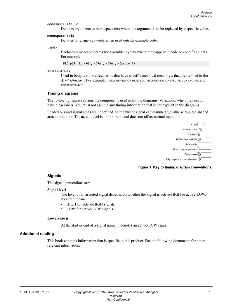
Timing diagrams
The following figure explains the components used in timing diagrams. Variations, when they occur,have clear labels. You must not assume any timing information that is not explicit in the diagrams.
Shaded bus and signal areas are undefined, so the bus or signal can assume any value within the shadedarea at that time. The actual level is unimportant and does not affect normal operation.
Clock
HIGH to LOW
Transient
HIGH/LOW to HIGH
Bus stable
Bus to high impedance
Bus change
High impedance to stable bus
Figure 1 Key to timing diagram conventions
Signals
The signal conventions are:
Signal levelThe level of an asserted signal depends on whether the signal is active-HIGH or active-LOW.Asserted means:• HIGH for active-HIGH signals.• LOW for active-LOW signals.
Lowercase n
At the start or end of a signal name, n denotes an active-LOW signal.
Additional reading
This book contains information that is specific to this product. See the following documents for otherrelevant information.
Preface About this book
101051_0002_02_en Copyright © 2019, 2020 Arm Limited or its affiliates. All rightsreserved.
13
Non-Confidential
Arm publications• Arm®v8-M Architecture Reference Manual (DDI 0553)• Arm® AMBA® 5 AHB Protocol Specification (IHI 0033)• AMBA® APB Protocol Version 2.0 Specification (IHI 0033)• AMBA® 4 ATB Protocol Specification (IHI 0032)• AMBA® AXI and ACE Protocol Specification (IHI 0022)• Arm® CoreSight™ System-on-Chip SoC-600 Technical Reference Manual (100806)• AMBA® Low Power Interface Specification Arm® Q-Channel and P-Channel Interfaces (IHI
0068)• Arm® Embedded Trace Macrocell Architecture Specification ETMv4 (ARM IHI 0064)• Arm® CoreSight™ Architecture Specification v3.0 (IHI 0029)• Arm® Debug Interface Architecture Specification, ADIv6.0 (IHI 0074)• Arm® Reliability, Availability, and Serviceability (RAS) Specification (DDI 0587)• Arm® CoreSight™ ETM‑M55 Technical Reference Manual (101053)• Arm®v8.1‑M Performance Monitoring User Guide Application Note
(ARM051-799564642-251 )
The following confidential book is only available to licensees:• Arm® Cortex®-M55 Processor Integration and Implementation Manual (101052)
Other publications• IEEE Std 1149.1-2001, Test Access Port and Boundary-Scan Architecture (JTAG)• ANSI/IEEE Std 754-2008, IEEE Standard for Binary Floating-Point Arithmetic
Preface About this book
101051_0002_02_en Copyright © 2019, 2020 Arm Limited or its affiliates. All rightsreserved.
14
Non-Confidential
Feedback
Feedback on this product
If you have any comments or suggestions about this product, contact your supplier and give:• The product name.• The product revision or version.• An explanation with as much information as you can provide. Include symptoms and diagnostic
procedures if appropriate.
Feedback on content
If you have comments on content then send an e-mail to [email protected]. Give:
• The title Arm Cortex-M55 Processor Technical Reference Manual.• The number 101051_0002_02_en.• If applicable, the page number(s) to which your comments refer.• A concise explanation of your comments.
Arm also welcomes general suggestions for additions and improvements. Note
Arm tests the PDF only in Adobe Acrobat and Acrobat Reader, and cannot guarantee the quality of therepresented document when used with any other PDF reader.
Preface Feedback
101051_0002_02_en Copyright © 2019, 2020 Arm Limited or its affiliates. All rightsreserved.
15
Non-Confidential
Chapter 1Introduction
This chapter provides an overview of the Cortex-M55 processor and its features.
It contains the following sections:• 1.1 Cortex®-M55 processor overview on page 1-17.• 1.2 Cortex®-M55 features on page 1-18.• 1.3 Supported standards and specifications on page 1-21.• 1.4 Design tasks on page 1-23.• 1.5 Documentation on page 1-24.• 1.6 Product revisions on page 1-25.
101051_0002_02_en Copyright © 2019, 2020 Arm Limited or its affiliates. All rightsreserved.
1-16
Non-Confidential
1.1 Cortex®-M55 processor overviewThe Cortex-M55 processor is a fully synthesizable mid-range microcontroller class processor thatimplements the Armv8.1‑M Mainline architecture that includes support for the M‑profile VectorExtension (MVE). The processor also supports previous Armv8‑M architectural features.
The design is focused on compute applications such as Digital Signal Processing (DSP) and machinelearning. The Cortex-M55 processor is energy efficient and achieves high compute performance acrossscalar and vector operations while maintaining low power consumption.
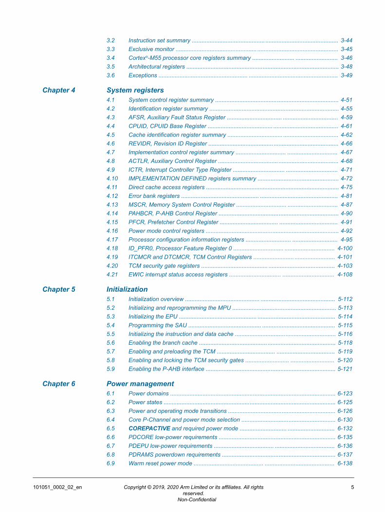
The following figure shows the Cortex-M55 processor in a typical system.
DMA
Processor
GPIO
SRAM
Peripherals
S-AHB
FLASH
P-AHBITCM DTCM M-AXI
External memory
AHB matrix
Figure 1-1 Example processor system
For more information on the processor-level components, see 2.1 Cortex®-M55 processor componentson page 2-27.
1 Introduction1.1 Cortex®-M55 processor overview
101051_0002_02_en Copyright © 2019, 2020 Arm Limited or its affiliates. All rightsreserved.
1-17
Non-Confidential
1.2 Cortex®-M55 featuresThe Cortex-M55 processor implements the Armv8.1‑M Mainline architecture and also supports previousArmv8‑M architectural features.
For more information on Armv8‑M and Armv8.1‑M features and variants information, see the Arm®v8‑Mvariants section in the Arm®v8-M Architecture Reference Manual.
Note
• The 'Optional' column indicates a feature that can be optionally included, either by:— Setting relevant RTL parameters. For example, if you include the Instrumentation Trace
Macrocell (ITM).— Being optionally licensed. For example, if you optionally license ETM-Cortex-M55.
• The 'Configurable' column indicates a feature that can be configured to any permitted value by settingrelevant RTL parameters. For example, you can configure the size of the instruction and data cache tobe 4KB, 8KB, 16KB, 32KB, or 64KB.
Table 1-1 Cortex-M55 processor features
Feature Architectureversion
Alwayspresent?
Optional? Configurable? Details
Arm PMSAv8 memorysystem architecture withmemory protection
- Yes - - -
Arm FPv5 hardwaresupporting scalar half, single,and double-precisionfloating-point operation thatis compliant withIEEE754-2008
Armv8‑M onwards - Yes - Optionally licensable component
DSP Extension Armv8‑M onwards Yes - - -
DSP Debug Extension Armv8.1‑M Yes - - -
Exception model Armv8‑M onwards Yes - - See 3.6 Exceptions on page 3-49for more information.
External ImplementationDefined Attribution Unit(IDAU)
- Yes - - Can be used only when theSecurity Extension is enabled
Level 1 (L1) instruction anddata cache.
Armv8‑M onwards - Yes Yes -
Main Extension Armv8.1‑M Yes - - Includes the 16-bit and 32-bitThumb instruction set
Memory Protection Unit(MPU)
Armv8‑M onwards - Yes Yes Supports up to 16 regions eachfor Secure and Non-secureapplications
1 Introduction1.2 Cortex®-M55 features
101051_0002_02_en Copyright © 2019, 2020 Arm Limited or its affiliates. All rightsreserved.
1-18
Non-Confidential
Table 1-1 Cortex-M55 processor features (continued)
Feature Architectureversion
Alwayspresent?
Optional? Configurable? Details
MVE, supporting SingleInstruction Multiple Data(SIMD) 128-bit vectoroperations
Armv8.1‑M - Yes - Supported data types are:• Integer• Half precision floating-point
(supported when floating-point functionality isincluded)
• Single precision floating-point (supported whenfloating-point functionality isincluded)
MVE is also referred to as ArmHelium™ technology
Support for DataIndependent Timing (DIT)operation
Armv8.1‑M Yes - - See the Arm®v8-M ArchitectureReference Manual.
Nested Vector InterruptController (NVIC)
Armv8‑M onwards Yes - Yes Supports up to 480 externalinterrupts with up to 256 prioritylevels
Reliability, Availability, andServiceability (RAS)Extension
Armv8.1‑M Yes - - -
Security Attribution Unit(SAU)
Armv8‑M onwards - Yes Yes Supports up to eight Non-secureor Non-secure Callable memoryregions
Security Extension Armv8‑M onwards - Yes - The Security Extension is animplementation of ArmTrustZone® technology
Unprivileged DebugExtension (UDE)
Armv8.1‑M Yes - - -
Debug and trace features
The following table shows the debug and trace features of the processor.
Table 1-2 Debug and trace features
Feature Architecture version Alwayspresent?
Optional? Configurable? Details
Breakpoint Unit (BPU)and comparator support
Armv8‑M onwards - Yes Yes Four or eight comparators aresupported
Data Watchpoint andTrace (DWT) unit andcomparator support
Armv8‑M onwards - Yes Yes Supports the PerformanceMonitoring Unit (PMU). Twoor four comparators aresupported
Embedded TraceMacrocell (ETM)
Arm (ETM) v4.5 - Yes - Optionally licensablecomponent.
1 Introduction1.2 Cortex®-M55 features
101051_0002_02_en Copyright © 2019, 2020 Arm Limited or its affiliates. All rightsreserved.
1-19
Non-Confidential
Table 1-2 Debug and trace features (continued)
Feature Architecture version Alwayspresent?
Optional? Configurable? Details
ITM Armv8‑M onwards - Yes -
PMU Armv8.1‑M - Yes - Present when the DWT isincluded
1 Introduction1.2 Cortex®-M55 features
101051_0002_02_en Copyright © 2019, 2020 Arm Limited or its affiliates. All rightsreserved.
1-20
Non-Confidential
1.3 Supported standards and specificationsThe Cortex-M55 processor complies with, or implements, the relevant Arm architectural standards andprotocols.
This book complements architecture reference manuals, architecture specifications, protocolspecifications, and relevant external standards. It does not duplicate information from these sources.
Arm architecture
The Cortex-M55 processor is compliant with the Armv8.1‑M Mainline architecture and also supportsprevious Armv8‑M architectural features. See 1.2 Cortex®-M55 features on page 1-18 for moreinformation.
Bus architecture
The Cortex-M55 processor implements AMBA 5 AXI-compliant Master AXI (M-AXI) interface for slowon-chip or off-chip memory and devices.
It also provides external interfaces that comply with the AMBA 5 AHB protocol.
Additionally, the Cortex-M55 processor implements interfaces for CoreSight and other debugcomponents using the AMBA 4 APB protocol (this is the same as APB protocol version 2.0) andATBv1.1 part of the AMBA 4 ATB protocol.
For more information, see the:• AMBA® AXI and ACE Protocol Specification• Arm® AMBA® 5 AHB Protocol Specification.• AMBA® APB Protocol Version 2.0 Specification.• AMBA® 4 ATB Protocol Specification.
The Cortex-M55 processor also provides P-Channel and Q-Channel interfaces for power and clockcontrol. See the AMBA® Low Power Interface Specification Arm® Q-Channel and P-Channel Interfaces.
For more overview information on bus interfaces, see 2.2 Interfaces on page 2-34.
Debug
The debug features of the Cortex-M55 processor implement the Arm Debug Interface v6.0 architecture.
See the Arm® Debug Interface Architecture Specification, ADIv6.0.
Embedded Trace Macrocell
The trace features of the Cortex-M55 processor implement the Arm Embedded Trace Macrocell (ETM)v4.5 architecture.
See the Arm® CoreSight™ ETM‑M55 Technical Reference Manual for more information on ETM-Cortex-M55 which is an optional component that you can license.
Extension Processing Unit
The Extension Processing Unit (EPU) performs scalar floating-point and vector operations.
The EPU is configured to include a scalar floating-point functionality, which supports half-precision,single-precision, and double-precision arithmetic as defined by the Arm FPv5 architecture.
The EPU implements MVE, which can support:• Half-precision, single-precision, and double-precision floating-point.• Integer, half-precision, and single-precision vector arithmetic.
See 2.6 Cortex®-M55 implementation options on page 2-39.
1 Introduction1.3 Supported standards and specifications
101051_0002_02_en Copyright © 2019, 2020 Arm Limited or its affiliates. All rightsreserved.
1-21
Non-Confidential

The Cortex-M55 processor provides floating-point computation functionality that is included withFloating-point and MVE, which is compliant with the ANSI/IEEE Std 754-2008, IEEE Standard forBinary Floating-Point Arithmetic.
1 Introduction1.3 Supported standards and specifications
101051_0002_02_en Copyright © 2019, 2020 Arm Limited or its affiliates. All rightsreserved.
1-22
Non-Confidential
1.4 Design tasksThe Cortex-M55 processor is delivered as synthesizable RTL that must go through implementation,integration, and programming processes before you can use it in a product.
The following definitions describe each top-level process in the design flow:
ImplementationThe implementer configures and synthesizes the RTL.
IntegrationThe integrator connects the Cortex-M55 processor into an SoC. This includes connecting it to amemory system and peripherals.
ProgrammingThe system programmer develops the software required to configure and initialize the Cortex-M55 processor and tests the required application software.
Implementation and integration choices affect the behavior and features of the Cortex-M55 processor.
The operation of the final device depends on:
Build configurationThe implementer chooses the options that affect how the RTL source files are pre-processed.These options usually include or exclude logic that affects one or more of the area, maximumfrequency, and features of the resulting macrocell.
Configuration inputsThe integrator configures some features of the Cortex-M55 processor by tying inputs to specificvalues. These configurations affect the start-up behavior before any software configuration ismade. They can also limit the options available to the software.
Software configurationThe programmer configures the Cortex-M55 processor by programming particular values intoregisters. This affects the behavior of the Cortex-M55 processor.
Note
This manual refers to IMPLEMENTATION-DEFINED features that are applicable to build configuration options.Reference to a feature that is included means that the appropriate build and signal configuration optionshave been selected. Reference to an enabled feature means that software has also configured the feature.
1 Introduction1.4 Design tasks
101051_0002_02_en Copyright © 2019, 2020 Arm Limited or its affiliates. All rightsreserved.
1-23
Non-Confidential
1.5 DocumentationThe Cortex-M55 processor documentation can help you complete the top-level processes ofimplementation, integration, and programming that are required to use the product correctly.
The Cortex-M55 processor documentation includes a Technical Reference Manual, an Integration andImplementation Manual, and User Guide Reference Material.
Technical Reference ManualThe Technical Reference Manual (TRM) describes the functionality and the effects of functionaloptions on the behavior of the Cortex-M55 processor. It is required at all stages of the designflow. Some behavior described in the TRM might not be relevant because of the way that theCortex-M55 processor is implemented and integrated. If you are programming the Cortex-M55processor, then contact the implementer to determine:• The build configuration of the implementation.• What integration, if any, was performed before implementing the Cortex-M55 processor.
Integration and Implementation ManualThe Integration and Implementation Manual (IIM) describes:• The available build configuration options and related issues in selecting them.• How to configure the Register Transfer Level (RTL) with the build configuration options.• How to integrate the Cortex-M55 processor into an SoC. This includes a description of the
integration kit and describes the pins that the integrator must tie off to configure themacrocell for the required integration.
• How to implement the Cortex-M55 processor into your design. This includes Memory Built-In Self Test (MBIST) and Design for Test (DFT) information, and information how toperform netlist dynamic verification on the Cortex-M55 processor.
• The processes to sign off the integration and implementation of the design.
The Arm product deliverables include reference scripts and information about using them toimplement your design.
Reference methodology documentation from your EDA tools vendor and the implementationReference Methodology (iRM) readme.txt provided by Arm complements the IIM.
The IIM is a confidential book that is only available to licensees.
User Guide Reference MaterialThis document provides reference material that Arm partners can configure and include in aUser Guide for an Arm Cortex-M55 processor. Typically:• Each chapter in this reference material might correspond to a section in the User Guide.• Each top-level section in this reference material might correspond to a chapter in the User
Guide.
However, you can organize this material in any way, subject to the conditions of the licenseagreement under which Arm supplied the material.
See the Additional reading on page 13 for more information about the books that are associated with theCortex-M55 processor.
1 Introduction1.5 Documentation
101051_0002_02_en Copyright © 2019, 2020 Arm Limited or its affiliates. All rightsreserved.
1-24
Non-Confidential
1.6 Product revisionsThe following product revisions have been released.
r0p0 First release for Beta r0p0.First limited access release for r0p0.
r0p1 First early access release for r0p1.r0p2 First release for r0p2.
Second release for r0p2.
1 Introduction1.6 Product revisions
101051_0002_02_en Copyright © 2019, 2020 Arm Limited or its affiliates. All rightsreserved.
1-25
Non-Confidential
Chapter 2Technical overview
This chapter describes the Cortex-M55 processor components and configuration options.
It contains the following sections:• 2.1 Cortex®-M55 processor components on page 2-27.• 2.2 Interfaces on page 2-34.• 2.3 Security on page 2-36.• 2.4 Reliability on page 2-37.• 2.5 Power intent on page 2-38.• 2.6 Cortex®-M55 implementation options on page 2-39.
101051_0002_02_en Copyright © 2019, 2020 Arm Limited or its affiliates. All rightsreserved.
2-26
Non-Confidential
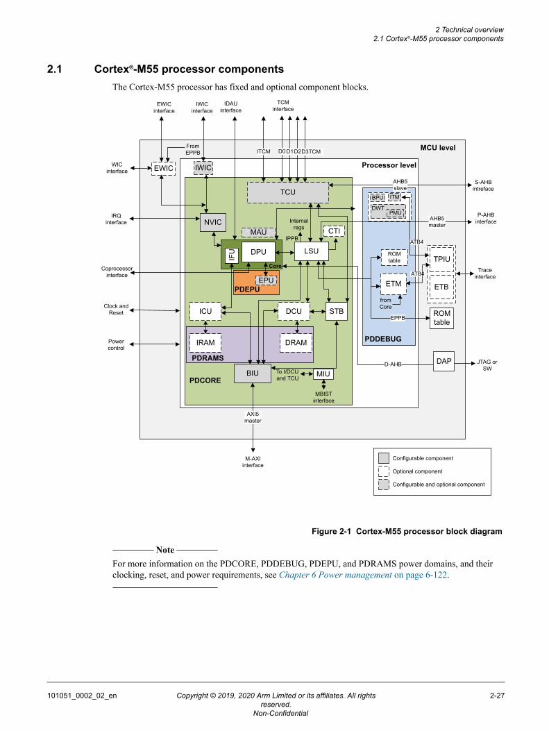
2.1 Cortex®-M55 processor componentsThe Cortex-M55 processor has fixed and optional component blocks.
PDRAMS
MBIST interface
TCU
LSU
PDEPUEPU
MAU
DPU
NVIC
ICU
IRAM
DCU
DRAM
BIU
STB
AHB5slave
AHB5master
AXI5master
ETM
CTI
ROM table
IPPB
IWIC
MIU
IFU
fromCore
Internalregs
DAP
TPIU
ROMtable
EPPB
WIC interface
JTAG or SW
IDAU interface
TCM interface
M-AXIinterface
Traceinterface
P-AHBinterface
S-AHBintreface
IRQinterface
Clock and Reset
Power control
MCU level
Processor level
ATB4
DWT
IWIC interface
EWIC
PDCORE
PDDEBUG
Core
ETB
ATB4Coprocessor
interface
ITMBPU
PMU
D-AHBPDRAMS
EWIC interface
ITCM D0 D1D2From EPPB TCMD3
To I/DCU and TCU
Configurable component
Optional component
Configurable and optional component
Figure 2-1 Cortex-M55 processor block diagram
Note
For more information on the PDCORE, PDDEBUG, PDEPU, and PDRAMS power domains, and theirclocking, reset, and power requirements, see Chapter 6 Power management on page 6-122.
2 Technical overview2.1 Cortex®-M55 processor components
101051_0002_02_en Copyright © 2019, 2020 Arm Limited or its affiliates. All rightsreserved.
2-27
Non-Confidential
The following table describes the various processor components shown in the processor block diagram.
Table 2-1 Processor components
Block Component
Processor core See 2.1.1 Cortex®-M55 processor core on page 2-29.
ExtensionProcessing Unit(EPU)
The EPU performs:• Scalar floating-point operations• M-class Vector Extension (MVE) operations
For more information, see 2.1.2 Extension Processing Unit on page 2-29. The EPU can be optionally included.
Memorycomponents
The memory components are:• Memory Authentication Unit (MAU). For more information on MAU, see Memory Authentication Unit
on page 2-30 . The MAU contains:— Security Attribution Unit (SAU)— TCM Gate Unit (TGU)— Secure MPU region, MPU_S, which is always optionally configured— Non-secure MPU region, MPU_N, which is always optionally configured
• Load Store Unit (LSU)• TCM Control Unit (TCU)• Data Cache Unit (DCU) and Data RAM (DRAM).• Instruction Cache Unit (ICU) and Instruction RAM (IRAM)• Bus Interface Unit (BIU)• Store Buffer (STB)• MBIST Interface Unit (MIU)
For more information on the memory system, see Memory system on page 2-31.
Interruptcomponents
The interrupt components are:• Nested Vectored Interrupt Controller (NVIC)• External Wakeup Interrupt Controller (EWIC), which can be optionally included• Internal Wakeup Interrupt Controller (IWIC), which can be optionally included
For more information on the interrupt-related components, see 2.1.4 Interrupt components on page 2-32.
Debug and tracecomponents
The debug and trace components are:• BreakPoint unit (BPU)• Cross Trigger Interface (CTI), which is optionally configured• CoreSight-compliant Debug Access Port (DAP), CoreSight DAP-Lite2, which is available for download when
you license Cortex-M55 processor IP.• Data Watchpoint and Trace (DWT) unit• Performance Monitoring Unit (PMU), which is located in the DWT• Embedded Trace Macrocell (ETM), which is an optional licensable component.• Instrumentation Trace Macrocell (ITM)• Trace Port Interface Unit (TPIU)• CoreSight-compliant Embedded Trace Buffer (ETB) functionality support. The ETB is not delivered as a part
of the IP deliverable. The ETB is an optional licensable component which is available when you license eitherthe CoreSight SoC-600 or CoreSight SoC-600M. The Cortex-M55 IP deliverable has a placeholder for ETBintegration.
For more information on the debug and trace related components, see 2.1.5 Debug and trace componentson page 2-32.
2 Technical overview2.1 Cortex®-M55 processor components
101051_0002_02_en Copyright © 2019, 2020 Arm Limited or its affiliates. All rightsreserved.
2-28
Non-Confidential
Note
• If the Cortex-M55 processor is configured with minimal debug, then the ETM and ITM cannot beincluded.
• If the Cortex-M55 processor is configured with reduced set or full set debug, then the ETM and ITMare optional.
• If the Cortex-M55 processor is configured with the reduced set or the full set debug, then the BPUand DWT are always included.
2.1.1 Cortex®-M55 processor core
The Cortex-M55 processor core has an Instruction Fetch Unit (IFU) that is closely coupled with the DataProcessing Unit (DPU).
The DPU contains the logic to:
• Decode and execute scalar integer instructions.• Handle the register transfer operations required for exception entry and exit.
The Cortex-M55 processor core has the following features:• An in-order four-stage integer pipeline with early completion of common arithmetic instructions.• Two Arithmetic Logic Units (ALUs):
— One ALU for regular shift and arithmetic operations, including limited support for dual-issue.— One ALU that can handle the SIMD operations included in the Digital Signal Processing (DSP)
Extension.• The core can handle up to two 32-bit vector load operations in parallel, when M‑profile Vector
Extension (MVE) is configured in the Cortex-M55 processor.• Harvard bus interfaces with vector fetch capability on the instruction side to optimize exception entry
for efficient operation of compute workloads.— 32-bit instruction fetch data width.— 64-bit load/store data width.
• Optimized set of integer register bank ports for energy-efficient operation.• Integer divide unit with support for operand-dependent early termination. In this context, early
termination refers to operations that terminate sooner than the expected number of cycles for theinteger divide unit. Early termination capabilities depend on the data that enters the pipeline.
• Single cycle branch latency in most instances, without a requirement for branch prediction.• Limited dual-issue of common 16-bit instruction pairs.• Support for exception-continuable load and store multiple accesses.• Instruction queue to decouple instruction fetching and instruction execution. This can also be used for
optimized vector processing when using the Low Overhead Branch (LOB) feature.• Data prefetch to minimize the effect of AXI latency when accessing consistent patterns of cacheable
data.
Note
The Cortex-M55 processor core works with the Extension Processing Unit (EPU), when configured toprovide full support for:• Integer and floating-point operations included in MVE.• Scalar half-precision, single-precision, and double-precision floating-point operations.
2.1.2 Extension Processing Unit
The Extension Processing Unit (EPU) includes support for all the instructions in the M‑profile VectorExtension (MVE) and half, single, and double-precision scalar FPv5 architecture.
2 Technical overview2.1 Cortex®-M55 processor components
101051_0002_02_en Copyright © 2019, 2020 Arm Limited or its affiliates. All rightsreserved.
2-29
Non-Confidential
The EPU has the following features:• MVE is implemented using a 64-bit arithmetic and load/store data-path in a two beats per tick
configuration. A beat is the execution of ¼ of an MVE instruction. Instructions can overlap to allowfull utilization of the logic with a sustained bandwidth of 64-bit Multiply ACcumulate (MAC) and 64-bit load/store per cycle. For more information on vector operation terminology, see Arm®v8-MArchitecture Reference Manual.
• Extended register file, which is optimized for efficient vector operations.• Floating-point MAC unit capable of a throughput of up to two single-precision or four-half precision
MAC instructions every cycle when MVE is included in the Cortex-M55 processor, or one single orhalf-precision MAC every cycle when only scalar floating-point is configured.
• Area optimized double-precision floating-point implementation.• Support for Security Extension including lazy context stacking.
2.1.3 Memory components
The Cortex-M55 processor memory components consist of the Memory Authentication Unit (MAU) andmemory system interfaces.
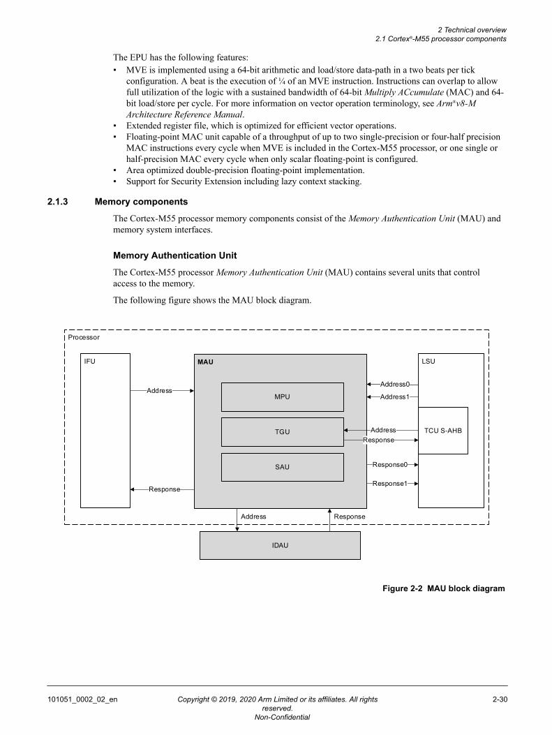
Memory Authentication Unit
The Cortex-M55 processor Memory Authentication Unit (MAU) contains several units that controlaccess to the memory.
The following figure shows the MAU block diagram.
Processor
MAU
MPU
TGU
SAU
IFU LSU
TCU S-AHB
IDAU
Address
Response
Address
Address1
Response
Response0
Response1
Address Response
Figure 2-2 MAU block diagram
2 Technical overview2.1 Cortex®-M55 processor components
101051_0002_02_en Copyright © 2019, 2020 Arm Limited or its affiliates. All rightsreserved.
2-30
Non-Confidential
Memory Protection UnitThe Memory Protection Unit (MPU) supports the Arm Protected Memory System Architecture(PMSA). Therefore, the MPU provides programmable support for memory protection usingmany software controllable regions. This unit defines the memory attributes that are associatedwith a particular memory region and the access permissions of addresses. Memory regions canbe programmed to generate faults when accessed inappropriately, for example, by unprivilegedsoftware, reducing the scope of incorrectly written application code. The architecture includesfault status registers to allow an exception handler to determine the source of the fault and toapply corrective action or notify the system.If the Security Extension is implemented, the entire MPU logic can be split into Secure andNon-secure MPU regions.
Security Attribution UnitThe Security Attribution Unit (SAU) defines and authenticates accesses to memory based on theSecurity state of the core or the debugger. These states can be any of the following:• Non-secure.• Secure and Non-secure Callable.• Secure.
TCM Gate UnitThe TCM Gate Unit (TGU) controls software and Slave AHB (S-AHB) accesses to the TCMsbased on the security attribute of the access.
Interface to the IDAUThe MAU contains an interface to the Implementation Defined Attribution Unit (IDAU), whichis present outside the core and not a part of the Cortex-M55 processor. This unit defines memoryregions as being either Secure, Non-secure, Non-secure Callable, or exempt from securitychecking. The final security mapping of memory regions is a combination of the response fromthe SAU and IDAU.
Memory system
The Cortex-M55 processor memory system provides the interface between the core and the caches,external memory interfaces, and internal memory-mapped registers.
The memory system includes:
• A single interface to an Instruction Tightly Coupled Memory (ITCM) and four interfaces to DataTightly Coupled Memories (DTCMs), D0TCM, D1TCM, D2TCM, and D3TCM
• A Master AXI (M-AXI) interface that can be used for on-chip or off-chip memory and devices• A Peripheral AHB (P-AHB) for access to external peripherals• A Slave AHB (S-AHB) for system access to the TCMs• An L1 instruction cache• An L1 data cache• An External PPB (EPPB) APB interface for CoreSight debug and trace components• A STore Buffer (STB) to hold store operations when they have left the load/store pipeline and the
DPU has committed them. From the STB, a store can do any of the following:— Request access to the cache RAM through the DCU— Request the Bus Interface Unit (BIU) to initiate linefills— Request the BIU to write data on the M-AXI interface
If there are several store transactions that are associated with the same 64-bit aligned doubleword, theSTB can merge these store transactions into a single transaction.
For more information, see:• Chapter 7 Memory model on page 7-143.• Memory system on page 2-31.
2 Technical overview2.1 Cortex®-M55 processor components
101051_0002_02_en Copyright © 2019, 2020 Arm Limited or its affiliates. All rightsreserved.
2-31
Non-Confidential
2.1.4 Interrupt components
The Cortex-M55 processor interrupt components are responsible for low-latency interrupt processing andenabling the Cortex-M55 processor to enter and wake up from low-power state.
NVIC features
The Cortex-M55 processor Nested Vectored Interrupt Controller (NVIC) is closely integrated with thecore to achieve low-latency interrupt processing.
The NVIC is responsible for:• Maintaining the current execution priority of the Cortex-M55 processor.• Maintaining the pending and active status of all exceptions that are supported.• Invoking preemption when a pending exception has priority.• Providing wakeup signals to wakeup the Cortex-M55 processor from deep sleep mode.• Providing support to the Internal Wakeup Interrupt Controller (IWIC) and External Wakeup Interrupt
Controller (EWIC).• Providing priority and exception information to other processor components.
The NVIC in the Cortex-M55 processor allows up to 496 exceptions, of which, 480 can be regularexternal interrupts.
Wakeup Interrupt Controller
The Cortex-M55 processor supports a Wakeup Interrupt Controller (WIC) unit that allows the Cortex-M55 processor to enter low-power state.
There are two WICs that are supported:
• An Internal Wakeup Interrupt Controller (IWIC) that is synchronous with the processor andcontained within the Cortex-M55 processor boundary.
• An External Wakeup Interrupt Controller (EWIC), which is a system-level component that can beasynchronous to the Cortex-M55 processor.
The Cortex-M55 processor supports any of the following:• No WIC.• IWIC only.• EWIC only.• Both IWIC and EWIC.
2.1.5 Debug and trace components
The Cortex-M55 processor has optional and configurable debug and trace components.
Breakpoint UnitA configurable Breakpoint Unit (BPU) for implementing breakpoints.
Data Watchpoint and TraceA configurable Data Watchpoint and Trace (DWT) unit for implementing watchpoints, datatracing, and system profiling.
Instrumentation Trace MacrocellAn optional Instrumentation Trace Macrocell (ITM) that supports printf() style debuggingusing instrumentation trace.
Performance Monitoring UnitA Performance Monitoring Unit (PMU) which enables software and debugger to gatherstatistics on events taking place on the Cortex-M55 processor. These statistics can be used forperformance analysis and system debug.The PMU is always present when the DWT is present.
2 Technical overview2.1 Cortex®-M55 processor components
101051_0002_02_en Copyright © 2019, 2020 Arm Limited or its affiliates. All rightsreserved.
2-32
Non-Confidential
ROM tablesROM tables allow debuggers to determine which CoreSight components are implemented in theCortex-M55 processor.
Debug and trace interfacesThese interfaces are suitable for:• Passing on-chip data through a Trace Port Interface Unit (TPIU) to a Trace Port Analyzer
(TPA), including Serial Wire Output (SWO) mode.• Integrating a Debug Access Port (DAP), which is a debug port that is used to control debug
functionality.• Integrating a CoreSight Embedded Trace Buffer (ETB), which is an optional licensable
component for trace data to be written to an external SRAM.
Cross Trigger InterfaceThe optional Cross Trigger Interface (CTI) enables the debug logic and Embedded TraceMacrocell (ETM) to interact with each other and with other CoreSight components.
Embedded Trace MacrocellThe optional ETM provides instruction-only trace capabilities. For more information, see theArm® CoreSight™ ETM‑M55 Technical Reference Manual.
2 Technical overview2.1 Cortex®-M55 processor components
101051_0002_02_en Copyright © 2019, 2020 Arm Limited or its affiliates. All rightsreserved.
2-33
Non-Confidential
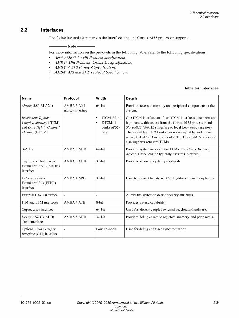
2.2 InterfacesThe following table summarizes the interfaces that the Cortex-M55 processor supports.
Note
For more information on the protocols in the following table, refer to the following specifications:• Arm® AMBA® 5 AHB Protocol Specification.• AMBA® APB Protocol Version 2.0 Specification.• AMBA® 4 ATB Protocol Specification.• AMBA® AXI and ACE Protocol Specification.
Table 2-2 Interfaces
Name Protocol Width Details
Master AXI (M-AXI) AMBA 5 AXImaster interface
64-bit Provides access to memory and peripheral components in thesystem.
Instruction TightlyCoupled Memory (ITCM)and Data Tightly CoupledMemory (DTCM)
- • ITCM: 32-bit• DTCM: 4
banks of 32-bits
One ITCM interface and four DTCM interfaces to support andhigh-bandwidth access from the Cortex-M55 processor andSlave AHB (S-AHB) interface to local low-latency memory.The size of both TCM instances is configurable, and in therange, 4KB-16MB in powers of 2. The Cortex-M55 processoralso supports zero size TCMs.
S-AHB AMBA 5 AHB 64-bit Provides system access to the TCMs. The Direct MemoryAccess (DMA) engine typically uses this interface.
Tightly coupled masterPeripheral AHB (P-AHB)interface
AMBA 5 AHB 32-bit Provides access to system peripherals.
External PrivatePeripheral Bus (EPPB)interface
AMBA 4 APB 32-bit Used to connect to external CoreSight-compliant peripherals.
External IDAU interface - - Allows the system to define security attributes.
ITM and ETM interfaces AMBA 4 ATB 8-bit Provides tracing capability.
Coprocessor interface - 64-bit Used for closely-coupled external accelerator hardware.
Debug AHB (D-AHB)slave interface
AMBA 5 AHB 32-bit Provides debug access to registers, memory, and peripherals.
Optional Cross TriggerInterface (CTI) interface
- Four channels Used for debug and trace synchronization.
2 Technical overview2.2 Interfaces
101051_0002_02_en Copyright © 2019, 2020 Arm Limited or its affiliates. All rightsreserved.
2-34
Non-Confidential
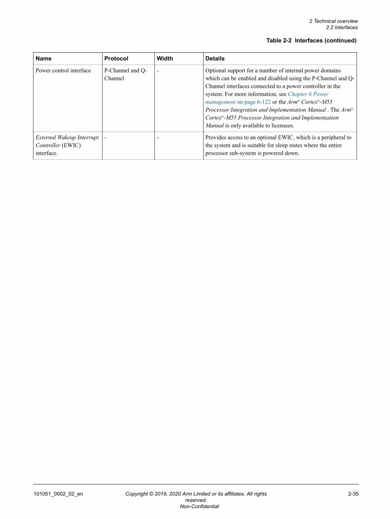
Table 2-2 Interfaces (continued)
Name Protocol Width Details
Power control interface P-Channel and Q-Channel
- Optional support for a number of internal power domainswhich can be enabled and disabled using the P-Channel and Q-Channel interfaces connected to a power controller in thesystem. For more information, see Chapter 6 Powermanagement on page 6-122 or the Arm® Cortex®-M55Processor Integration and Implementation Manual . The Arm®
Cortex®-M55 Processor Integration and ImplementationManual is only available to licensees.
External Wakeup InterruptController (EWIC)interface.
- - Provides access to an optional EWIC, which is a peripheral tothe system and is suitable for sleep states where the entireprocessor sub-system is powered down.
2 Technical overview2.2 Interfaces
101051_0002_02_en Copyright © 2019, 2020 Arm Limited or its affiliates. All rightsreserved.
2-35
Non-Confidential
2.3 SecurityArm TrustZone technology uses the Security Extension, which supports Secure and Non-secure states onall memory interfaces, including security gating on Tightly Coupled Memory (TCM) interfaces.
Memory and peripherals in the system can be marked as Secure, making them accessible only to codethat is running in the Secure state.
Interrupts can be marked as Secure indicating that they are handled by Secure handler code in the Secureworld.
Hardware protects all Secure resources, including firmware and sensitive data values from being visibleto Non-secure code and debug. If you are programming in Secure state, you can choose which Securefunctions can be called by Non-secure code, where the Secure functions can tightly control theparameters of such function calls.
2 Technical overview2.3 Security
101051_0002_02_en Copyright © 2019, 2020 Arm Limited or its affiliates. All rightsreserved.
2-36
Non-Confidential
2.4 ReliabilityThe Cortex-M55 processor reliability features include:
• L1 cache and TCM interfaces support optional internal Error Correcting Code (ECC). ECC errors arereported to the system on an external interface.
• Reliability, Availability, and Serviceability (RAS) Extension support.• Optional interface protection included on the M-AXI, S-AHB, P-AHB, Debug AHB (D-AHB), and
EPPB interfaces.
2 Technical overview2.4 Reliability
101051_0002_02_en Copyright © 2019, 2020 Arm Limited or its affiliates. All rightsreserved.
2-37
Non-Confidential
2.5 Power intentThe Cortex-M55 processor power intent features include:
• Support for multiple power domain State Retention Power Gating (SRPG) implementation throughUnified Power Format (UPF). The UPF files are IEEE 1801-2009 compliant.
• Power control based on the Arm standard P-Channel and Q-Channel interfaces. For information onthe P-Channel and Q-Channel logic interfaces, see AMBA® Low Power Interface Specification Arm®
Q-Channel and P-Channel Interfaces.• Support for an Internal Wakeup Interrupt Controller (IWIC) and an External Wakeup Interrupt
Controller (EWIC).
2 Technical overview2.5 Power intent
101051_0002_02_en Copyright © 2019, 2020 Arm Limited or its affiliates. All rightsreserved.
2-38
Non-Confidential
2.6 Cortex®-M55 implementation optionsThe Cortex-M55 processor has configurable options that the chip designer can set during theimplementation and integration stages to match your functional requirements.
The following table shows the Cortex-M55 processor configurable option available at implementationtime.
Table 2-3 Cortex-M55 processor configurable options
Feature Options
Floating-point and M‑profile Vector Extension(MVE) support
The floating-point and MVE features together specify the MVE functionality thatis supported on the Cortex-M55 processor.
Floating-point functionality can either be included or excluded.
If floating-point functionality is not included, then the MVE options can be eitherof the following:• MVE not included.• Integer subset of MVE included.
If floating-point functionality is included, then half-precision, single-precision,and double-precision floating-point operation is supported. The MVE options canbe any of the following:• MVE not included.• Integer subset of MVE included.• Integer, half-precision, and single-precision floating-point MVE are included.
Note
All other parameter combinations are invalid.
Inclusion of Security Extension No Security Extension present
Security Extension present
Coprocessor support No support for coprocessor hardware
Support for coprocessor hardware
Inclusion of Non-secure Memory Protection Unit(MPU)
0 region, 4 regions, 8 regions, 12 regions, or 16 regions
Inclusion of Secure Memory Protection Unit(MPU)
0 region, 4 regions, 8 regions, 12 regions, or 16 regions when the SecurityExtension is included.
Inclusion of Security Attribution Unit (SAU) 0 region, 4 regions, or 8 regions when the Security Extension is included.
Inclusion and size of instruction cache No Instruction Cache Unit (ICU)
ICU included and the size can be 4KB, 8KB, 16KB, 32KB, or 64KB
Inclusion and size of data cache Area optimized M-AXI interface, no Data Cache Unit (DCU)
DCU included and the size can be 4KB, 8KB, 16KB, 32KB, or 64KB
Inclusion of Error Correcting Code (ECC) No ECC on caches or TCMs
ECC on all implemented caches and TCMs
Number of interrupts 1-480 interrupts. To support non-contiguous mapping, you can remove individualinterrupts.
Number of exception priority bits 3-8 priority bits.
2 Technical overview2.6 Cortex®-M55 implementation options
101051_0002_02_en Copyright © 2019, 2020 Arm Limited or its affiliates. All rightsreserved.
2-39
Non-Confidential
Table 2-3 Cortex-M55 processor configurable options (continued)
Feature Options
Lowest interrupt latency interrupt numbers Specifies interrupt numbers which support the lowest interrupt latency and theinterrupt numbers which have one additional latency cycle.• 0 indicates lowest latency.• 1 indicates one additional latency cycle.
Disable support for individual interrupts When set to 1, support for individual interrupts is disabled, therefore, allowing arange of non-contiguous interrupts.
Debug resources included. This feature alsocontrols the number of Performance MonitoringUnit (PMU) counters that are present.
Minimal debug. No Halting debug or memory and peripheral access.
Reduced set. Two data watchpoint comparators and four breakpoint comparators.
Full set. Four data watchpoint comparators and eight breakpoint comparators.
Inclusion of Instrumentation Trace Macrocell(ITM) and Data Watchpoint and Trace (DWT)trace
No ITM or DWT trace
Complete ITM and DWT trace
Inclusion of Embedded Trace Macrocell (ETM) No ETM support
ETM instruction execution trace
Inclusion of Cross Trigger Interface (CTI) No CTI
CTI is included
Inclusion of Internal Wakeup Interrupt Controller(IWIC)
No IWIC
IWIC is included
Number of IRQ lines supported by the IWIC andEWIC
The value always includes the three internal events NMI, RXEV, Debug monitorevent, and at least one IRQ.
Inclusion of interface protection No interface protection
Interface protection is included. Interface protection provides parity bits to the businterface to help with fault coverage in functional safety applications.
Inclusion of ITCM security gating No ITCM security gate
ICTM security gate included
ITCM security gate block size in bytes 2(Instruction TCM Gate Unit (TGU) block size+5).
Number of ITCM security gate blocks 2Maximum number of instruction TGU blocks
Inclusion of DTCM security gating No DTCM security gate
DCTM security gate included
DTCM security gate block size in bytes 2(Data TGU block size+5)
Number of DTCM security gate blocks 2Maximum number of data TGU blocks
Reset all registers functionality Specifies whether all synchronous states or only the architecturally required statesare reset.• Only reset states that architecture requires.• Reset all synchronous states.
Note
• The parameter to control inclusion of the External Wakeup Interrupt Controller (EWIC) can beconfigured at the MCU level. The MCU level supports all the processor-level configuration and
2 Technical overview2.6 Cortex®-M55 implementation options
101051_0002_02_en Copyright © 2019, 2020 Arm Limited or its affiliates. All rightsreserved.
2-40
Non-Confidential
contains additional configuration parameters to configure the functionality that is specific toCoreSight components that are included in the system.
• Signal tie-offs determine the inclusion of the ITCM and DTCM.• Additionally, there are static and reset configuration signals. For more information, see C.3 Static
configuration signals on page Appx-C-379 and C.4 Reset configuration signals on page Appx-C-381.
2 Technical overview2.6 Cortex®-M55 implementation options
101051_0002_02_en Copyright © 2019, 2020 Arm Limited or its affiliates. All rightsreserved.
2-41
Non-Confidential
Chapter 3Programmers model
This chapter describes the Cortex-M55 processor register set, modes of operation, and providesinformation on programming the Cortex-M55 processor.
The Cortex-M55 programmers model is an implementation of the Main Extension architecture. For acomplete description of the programmers model, see the Arm®v8-M Architecture Reference Manual.
It contains the following sections:• 3.1 Security states, operation, and execution modes on page 3-43.• 3.2 Instruction set summary on page 3-44.• 3.3 Exclusive monitor on page 3-45.• 3.4 Cortex®-M55 processor core registers summary on page 3-46.• 3.5 Architectural registers on page 3-48.• 3.6 Exceptions on page 3-49.
101051_0002_02_en Copyright © 2019, 2020 Arm Limited or its affiliates. All rightsreserved.
3-42
Non-Confidential
3.1 Security states, operation, and execution modesThe Cortex-M55 processor supports Secure and Non-secure Security states, Thread and Handleroperating modes, and can run in either Thumb or Debug operating states. In addition, the Cortex-M55processor can limit or exclude access to some resources by executing code in privileged or unprivilegedmode.
See the Arm®v8-M Architecture Reference Manual for more information about the modes of operationand execution.
Security statesWhen the Security Extension is included in the Cortex-M55 processor, the programmers modelincludes two orthogonal Security states, Secure state and Non-secure state. This means theprocessor is in Secure or Non-secure state, but not both at the same time. When the SecurityExtension is implemented, the Cortex-M55 processor always resets into Secure state. When theSecurity Extension is not implemented, the Cortex-M55 processor resets into Non-secure state.Each Security state includes a set of independent operating modes and supports both privilegedand unprivileged user access. Registers in the System Control Space (SCS) are banked acrossSecure and Non-secure state, with the Non-secure register view available at an aliased address toSecure state.When the Security Extension is not included in the Cortex-M55 processor, the programmersmodel includes only the Non-secure state.
Operating modesFor each Security state, the Cortex-M55 processor can operate in Thread or Handler mode. Theconditions which cause the Cortex-M55 processor to enter Thread or Handler mode are asfollows:• The Cortex-M55 processor enters Thread mode on reset, or as a result of an exception return
to Thread mode. The Thread mode supports both privileged and unprivileged execution.• The Cortex-M55 processor enters Handler mode as a result of an exception. The Handler
mode only supports privileged execution.
The Cortex-M55 processor can change Security state on taking an exception. For example,when a Secure exception is taken from Non-secure state Thread or Handler mode, the Cortex-M55 processor enters the Secure state Handler mode.
The Cortex-M55 processor can also call Secure functions from Non-secure state and Non-securefunctions from Secure state. The Security Extension includes requirements for these calls toprevent secure data from being accessed in Non-secure state.
Operating statesThe Cortex-M55 processor can operate in T32 or Debug state:• T32 state is the state of normal execution running 16-bit and 32-bit halfword-aligned T32
instructions.• Debug state is the state when the Cortex-M55 processor is in Halting debug.
Privileged access and unprivileged user accessCode can execute as privileged or unprivileged. Unprivileged execution limits or excludesaccess to some resources appropriate to the current Security state. Privileged execution hasaccess to all resources available to the Security state. Handler mode is always privileged. Threadmode can be privileged or unprivileged.
3 Programmers model3.1 Security states, operation, and execution modes
101051_0002_02_en Copyright © 2019, 2020 Arm Limited or its affiliates. All rightsreserved.
3-43
Non-Confidential
3.2 Instruction set summaryThe Cortex-M55 processor implements the Armv8.1‑M instruction set.
These instructions include:• All base instructions• All instructions in the Main Extension• All instructions in the Digital Signal Processing (DSP) Extension• Optionally some of the coprocessor instructions. These are:
— CDP, CDP2— MCR, MCR2— MCRR, MCRR2— MRC, MRC2— MRRC, MRRC2
• Optionally all instructions in the Security Extension• Optionally all half-precision, single-precision, and double-precision instructions in the Floating-point
Extension• Optionally all vector operation instructions on integer operations in the M‑profile Vector Extension
(MVE)• Optionally all vector operation instructions on half-precision and single-precision floating-point
operations in MVE• Optionally all the Reliability, Availability, and Serviceability (RAS) Extension instructions
For more information about these instructions, see the Arm®v8-M Architecture Reference Manual.
3 Programmers model3.2 Instruction set summary
101051_0002_02_en Copyright © 2019, 2020 Arm Limited or its affiliates. All rightsreserved.
3-44
Non-Confidential
3.3 Exclusive monitorThe Cortex-M55 processor implements a local exclusive monitor contained in the Load Store Unit(LSU). The local monitor within the Cortex-M55 processor has been constructed not to hold any physicaladdress, but instead treats any store-exclusive access as matching the address of the previous load-exclusive.
This means that the implemented exclusives reservation granule is the entire memory address range. TheTCMs support a local exclusive monitor, but not shared or global exclusive monitors. This implies thatthe TCMs support for exclusive requests between threads running on the Cortex-M55 processor, but notexclusive requests between the Cortex-M55 processor and a DMA (through the S-AHB). If an exclusiveread access is carried out to a region which does not support a global monitor it must respondaccordingly with either HEXOKAY LOW or RRESP[1:0] OKAY. These responses result in thetransaction completing without setting the internal exclusive monitor. A subsequent exclusive storeinstruction does not carry out any memory transactions and sets the destination register to 1 indicatingthe exclusive access failed.
The external bus interfaces support a global exclusive monitor for address shared with other bus masters.
For more information about semaphores and the local exclusive monitor, see the Arm®v8-M ArchitectureReference Manual.
3 Programmers model3.3 Exclusive monitor
101051_0002_02_en Copyright © 2019, 2020 Arm Limited or its affiliates. All rightsreserved.
3-45
Non-Confidential
3.4 Cortex®-M55 processor core registers summaryThe Cortex-M55 processor core registers are 32 bits wide.
When the Security Extension is included, some of the registers are banked. The Secure view of theseregisters is available when the processor is in Secure state. The Non-secure view is available when theprocessor is in Non-secure and Secure state.
The following table shows the processor core register set summary. See the Arm®v8-M ArchitectureReference Manual for information about the Cortex-M55 processor core registers and their addresses,access types, and reset values.
Table 3-1 Processor core register set summary
Name Description
R0-R12 R0-R12 are general-purpose registers for data operations.
MSP (R13) The stack pointer, SP, is register R13. In Thread mode, the CONTROL register indicates the stack pointer touse, main stack pointer, MSP, or process stack pointer, PSP.
When the Security Extension is included, there are two MSP registers in the Cortex-M55 processor:
• MSP_NS for the Non-secure state.• MSP_S for the Secure state.
When the Security Extension is included, there are two PSP registers in the Cortex-M55 processor:• PSP_NS for the Non-secure state.• PSP_S for the Secure state.
PSP (R13)
MSPLIM The stack limit registers limit the extent to which the MSP and PSP registers can descend respectively.
When the Security Extension is included, there are two MSPLIM registers in the Cortex-M55 processor:
• MSPLIM_NS for the Non-secure state.• MSPLIM_S for the Secure state.
When the Security Extension is included, there are two PSPLIM registers in the Cortex-M55 processor:• PSPLIM_NS for the Non-secure state.• PSPLIM_S for the Secure state.
PSPLIM
LR (R14) The Link Register, LR, is register R14. It stores the return information for subroutines, function calls, andexceptions.
PC (R15) The Program Counter, PC, is register R15. It contains the current program address.
XPSR The Program Status Register, PSR, combines:• Application Program Status Register, APSR.• Interrupt Program Status Register, IPSR.• Execution Program Status Register, EPSR.
These registers provide different views of the PSR.
PRIMASK The PRIMASK register prevents activation of exceptions with configurable priority. For information about theException model the Cortex-M55 processor supports, see 3.6 Exceptions on page 3-49.
There are two PRIMASK registers in the Cortex-M55 processor:• PRIMASK_NS for the Non-secure state.• PRIMASK_S for the Secure state.
3 Programmers model3.4 Cortex®-M55 processor core registers summary
101051_0002_02_en Copyright © 2019, 2020 Arm Limited or its affiliates. All rightsreserved.
3-46
Non-Confidential
Table 3-1 Processor core register set summary (continued)
Name Description
BASEPRI The BASEPRI register defines the minimum priority for exception processing.
There are two BASEPRI registers in the Cortex-M55 processor:• BASEPRI_NS for the Non-secure state.• BASEPRI_S for the Secure state.
FAULTMASK The FAULTMASK register prevents activation of all exceptions except for non-maskable interrupt, NMI andoptionally Secure HardFault.
There are two FAULTMASK registers in the Cortex-M55 processor:• FAULTMASK_NS for the Non-secure state.• FAULTMASK_S for the Secure state.
LO_BRANCH_INFO Loop and branch tracking information. Software cannot access LO_BRANCH_INFO.
SP Current stack pointer register. SP_NS for the Non-secure state.
FPSCR Floating-point Status and Control Register
S0-S31 32 single-precision floating-point registers
D0-D15 16 double-precision floating-point registers
Q0-Q7 8 vector registers
VPR Vector Predication Status and Control Register
CONTROL The CONTROL register controls the stack that is used, and optionally the privilege level, when the Cortex-M55 processor is in Thread mode.
There are two CONTROL registers in the Cortex-M55 processor:• CONTROL_NS for the Non-secure state.• CONTROL_S for the Secure state.
3 Programmers model3.4 Cortex®-M55 processor core registers summary
101051_0002_02_en Copyright © 2019, 2020 Arm Limited or its affiliates. All rightsreserved.
3-47
Non-Confidential
3.5 Architectural registersArchitectural registers can be fully architectural or architectural with some IMPLEMENTATION DEFINED bitfields.
Information on fully architectural registers that are listed in this section, see the Arm®v8-M ArchitectureReference Manual. If registers are architectural with IMPLEMENTATION DEFINED bit fields, the registersummary table in this section links registers to their associated register description.
For more information on architectural registers, see:• 4.1 System control register summary on page 4-51.• 4.2 Identification register summary on page 4-55.• 4.5 Cache identification register summary on page 4-62
3 Programmers model3.5 Architectural registers
101051_0002_02_en Copyright © 2019, 2020 Arm Limited or its affiliates. All rightsreserved.
3-48
Non-Confidential
3.6 ExceptionsExceptions are handled and prioritized by the Cortex-M55 processor and the Nested Vectored InterruptController (NVIC). In addition to architecturally defined behavior, the Cortex-M55 processorimplements advanced exception and interrupt handling that reduces interrupt latency and includesIMPLEMENTATION DEFINED behavior.
3.6.1 Exception handling and prioritization
The Cortex-M55 processor core and the Nested Vectored Interrupt Controller (NVIC) together prioritizeand handle all exceptions.
When handling exceptions:
• All exceptions are handled in Handler mode.• Processor state is automatically stored to the stack on an exception, and automatically restored from
the stack at the end of the Interrupt Service Routine (ISR).• The vector is fetched in parallel to the state saving, enabling efficient interrupt entry.
The Cortex-M55 processor supports tail-chaining that enables back-to-back interrupts without theoverhead of state saving and restoration.
SoC designers configure the number of interrupts and bits of interrupt priority, during implementation.Software can choose only to enable a subset of the configured number of interrupts, and can choose howmany bits of the configured priorities to use.
When the Security Extension is included, exceptions can be programmed as either Secure or Non-secure.When an exception is taken, the Cortex-M55 processor switches to the associated Security state. Thepriority of Secure and Non-secure exceptions can be programmed independently. It is possible todeprioritize Non-secure configurable exceptions using AIRCR.PRIS to enable Secure interrupts to takepriority. When taking and returning from an exception, the register state is always stored using the stackpointer associated with the background Security state. When taking a Non-secure exception from Securestate, all the register states are stacked, and then the registers are cleared to prevent Secure data beingavailable to the Non-secure handler. The vector table base address is banked between Secure and Non-secure state. VTOR_S, contains the Secure vector table base address and VTOR_NS contains the Non-secure vector table base address. These registers can be programmed by software and also initialized atreset by the system.
If the Security Extension is not included all exceptions are Non-secure and only VTOR_NS is used todetermine the vector table base address.
Vector table entries are compatible with interworking between Arm and Thumb® instructions. Thiscauses bit[0] of the vector value to load into EPSR.T, on exception entry. All populated vectors in thevector table entries must have bit[0] set. Creating a vector table entry with bit[0] clear generates anINVSTATE (Invalid state flag) fault on the first instruction of the handler corresponding to this vector.
Input signals INITSVTOR[31:7] and INITNSVTOR[31:7] define the Secure and Non-secure vectortable base address, respectively. However, when the Security Extension is not implemented,INITNSVTOR[31:7] defines the vector table base address.
Note
• The Cortex-M55 processor abandons all multicycle instructions to take pending instructions.• Load Multiple and Store Multiple operations are interruptible.
3 Programmers model3.6 Exceptions
101051_0002_02_en Copyright © 2019, 2020 Arm Limited or its affiliates. All rightsreserved.
3-49
Non-Confidential
Chapter 4System registers
This chapter describes the system registers for the Cortex-M55 processor.
It contains the following sections:• 4.1 System control register summary on page 4-51.• 4.2 Identification register summary on page 4-55.• 4.3 AFSR, Auxiliary Fault Status Register on page 4-59.• 4.4 CPUID, CPUID Base Register on page 4-61.• 4.5 Cache identification register summary on page 4-62.• 4.6 REVIDR, Revision ID Register on page 4-66.• 4.7 Implementation control register summary on page 4-67.• 4.8 ACTLR, Auxiliary Control Register on page 4-68.• 4.9 ICTR, Interrupt Controller Type Register on page 4-71.• 4.10 IMPLEMENTATION DEFINED registers summary on page 4-72.• 4.11 Direct cache access registers on page 4-75.• 4.12 Error bank registers on page 4-81.• 4.13 MSCR, Memory System Control Register on page 4-87.• 4.14 PAHBCR, P-AHB Control Register on page 4-90.• 4.15 PFCR, Prefetcher Control Register on page 4-91.• 4.16 Power mode control registers on page 4-92.• 4.17 Processor configuration information registers on page 4-95.• 4.18 ID_PFR0, Processor Feature Register 0 on page 4-100.• 4.19 ITCMCR and DTCMCR, TCM Control Registers on page 4-101.• 4.20 TCM security gate registers on page 4-103.• 4.21 EWIC interrupt status access registers on page 4-108.
101051_0002_02_en Copyright © 2019, 2020 Arm Limited or its affiliates. All rightsreserved.
4-50
Non-Confidential
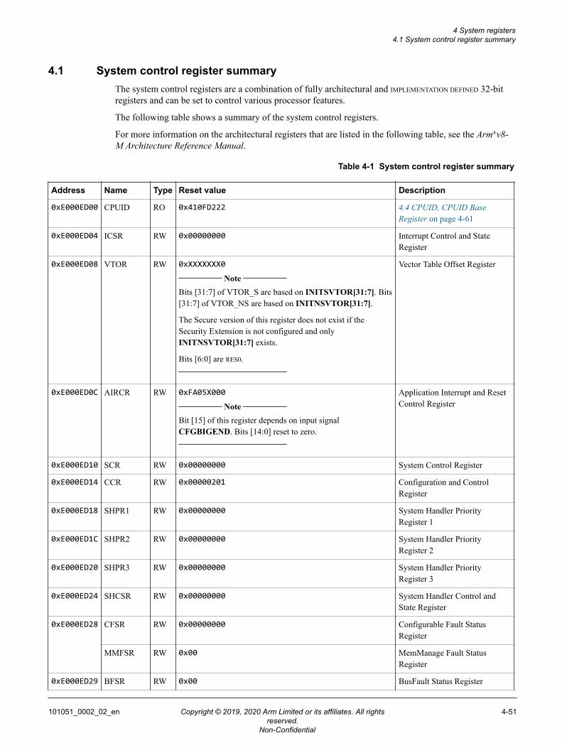
4.1 System control register summaryThe system control registers are a combination of fully architectural and IMPLEMENTATION DEFINED 32-bitregisters and can be set to control various processor features.
The following table shows a summary of the system control registers.
For more information on the architectural registers that are listed in the following table, see the Arm®v8-M Architecture Reference Manual.
Table 4-1 System control register summary
Address Name Type Reset value Description
0xE000ED00 CPUID RO 0x410FD222 4.4 CPUID, CPUID BaseRegister on page 4-61
0xE000ED04 ICSR RW 0x00000000 Interrupt Control and StateRegister
0xE000ED08 VTOR RW 0xXXXXXXX0 Note
Bits [31:7] of VTOR_S are based on INITSVTOR[31:7]. Bits[31:7] of VTOR_NS are based on INITNSVTOR[31:7].
The Secure version of this register does not exist if theSecurity Extension is not configured and onlyINITNSVTOR[31:7] exists.
Bits [6:0] are RES0.
Vector Table Offset Register
0xE000ED0C AIRCR RW 0xFA05X000 Note
Bit [15] of this register depends on input signalCFGBIGEND. Bits [14:0] reset to zero.
Application Interrupt and ResetControl Register
0xE000ED10 SCR RW 0x00000000 System Control Register
0xE000ED14 CCR RW 0x00000201 Configuration and ControlRegister
0xE000ED18 SHPR1 RW 0x00000000 System Handler PriorityRegister 1
0xE000ED1C SHPR2 RW 0x00000000 System Handler PriorityRegister 2
0xE000ED20 SHPR3 RW 0x00000000 System Handler PriorityRegister 3
0xE000ED24 SHCSR RW 0x00000000 System Handler Control andState Register
0xE000ED28 CFSR RW 0x00000000 Configurable Fault StatusRegister
MMFSR RW 0x00 MemManage Fault StatusRegister
0xE000ED29 BFSR RW 0x00 BusFault Status Register
4 System registers4.1 System control register summary
101051_0002_02_en Copyright © 2019, 2020 Arm Limited or its affiliates. All rightsreserved.
4-51
Non-Confidential
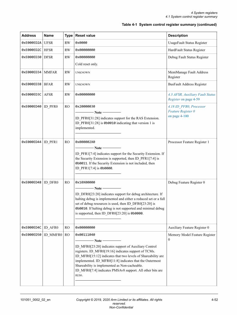
Table 4-1 System control register summary (continued)
Address Name Type Reset value Description
0xE000ED2A UFSR RW 0x0000 UsageFault Status Register
0xE000ED2C HFSR RW 0x00000000 HardFault Status Register
0xE000ED30 DFSR RW 0x00000000
Cold reset only.
Debug Fault Status Register
0xE000ED34 MMFAR RW UNKNOWN MemManage Fault AddressRegister
0xE000ED38 BFAR RW UNKNOWN BusFault Address Register
0xE000ED3C AFSR RW 0x00000000 4.3 AFSR, Auxiliary Fault StatusRegister on page 4-59
0xE000ED40 ID_PFR0 RO 0x20000030 Note
ID_PFR0[31:28] indicates support for the RAS Extension.ID_PFR0[31:28] is 0b0010 indicating that version 1 isimplemented.
4.18 ID_PFR0, ProcessorFeature Register 0on page 4-100
0xE000ED44 ID_PFR1 RO 0x000002X0 Note
ID_PFR1[7:4] indicates support for the Security Extension. Ifthe Security Extension is supported, then ID_PFR1[7:4] is0b0011. If the Security Extension is not included, thenID_PFR1[7:4] is 0b0000.
Processor Feature Register 1
0xE000ED48 ID_DFR0 RO 0x10X00000 Note
ID_DFR0[23:20] indicates support for debug architecture. Ifhalting debug is implemented and either a reduced set or a fullset of debug resources is used, then ID_DFR0[23:20] is0b0010. If halting debug is not supported and minimal debugis supported, then ID_DFR0[23:20] is 0b0000.
Debug Feature Register 0
0xE000ED4C ID_AFR0 RO 0x00000000 Auxiliary Feature Register 0
0xE000ED50 ID_MMFR0 RO 0x00111040 Note
ID_MFR0[23:20] indicates support of Auxiliary Controlregisters. ID_MFR0[19:16] indicates support of TCMs.ID_MFR0[15:12] indicates that two levels of Shareability areimplemented. ID_MFR0[11:8] indicates that the OutermostShareability is implemented as Non-cacheable.ID_MFR0[7:4] indicates PMSAv8 support. All other bits areRES0.
Memory Model Feature Register0
4 System registers4.1 System control register summary
101051_0002_02_en Copyright © 2019, 2020 Arm Limited or its affiliates. All rightsreserved.
4-52
Non-Confidential
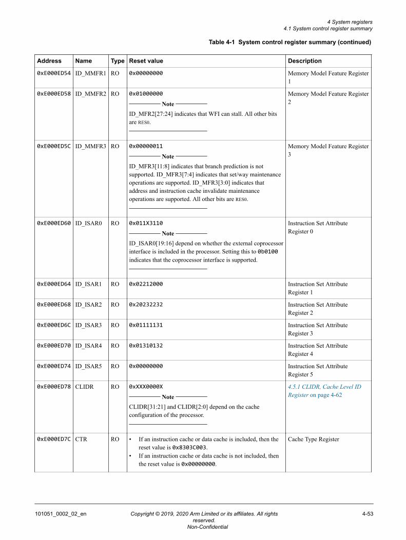
Table 4-1 System control register summary (continued)
Address Name Type Reset value Description
0xE000ED54 ID_MMFR1 RO 0x00000000 Memory Model Feature Register1
0xE000ED58 ID_MMFR2 RO 0x01000000 Note
ID_MFR2[27:24] indicates that WFI can stall. All other bitsare RES0.
Memory Model Feature Register2
0xE000ED5C ID_MMFR3 RO 0x00000011 Note
ID_MFR3[11:8] indicates that branch prediction is notsupported. ID_MFR3[7:4] indicates that set/way maintenanceoperations are supported. ID_MFR3[3:0] indicates thataddress and instruction cache invalidate maintenanceoperations are supported. All other bits are RES0.
Memory Model Feature Register3
0xE000ED60 ID_ISAR0 RO 0x011X3110 Note
ID_ISAR0[19:16] depend on whether the external coprocessorinterface is included in the processor. Setting this to 0b0100indicates that the coprocessor interface is supported.
Instruction Set AttributeRegister 0
0xE000ED64 ID_ISAR1 RO 0x02212000 Instruction Set AttributeRegister 1
0xE000ED68 ID_ISAR2 RO 0x20232232 Instruction Set AttributeRegister 2
0xE000ED6C ID_ISAR3 RO 0x01111131 Instruction Set AttributeRegister 3
0xE000ED70 ID_ISAR4 RO 0x01310132 Instruction Set AttributeRegister 4
0xE000ED74 ID_ISAR5 RO 0x00000000 Instruction Set AttributeRegister 5
0xE000ED78 CLIDR RO 0xXXX0000X Note
CLIDR[31:21] and CLIDR[2:0] depend on the cacheconfiguration of the processor.
4.5.1 CLIDR, Cache Level IDRegister on page 4-62
0xE000ED7C CTR RO • If an instruction cache or data cache is included, then thereset value is 0x8303C003.
• If an instruction cache or data cache is not included, thenthe reset value is 0x00000000.
Cache Type Register
4 System registers4.1 System control register summary
101051_0002_02_en Copyright © 2019, 2020 Arm Limited or its affiliates. All rightsreserved.
4-53
Non-Confidential
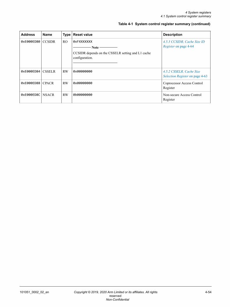
Table 4-1 System control register summary (continued)
Address Name Type Reset value Description
0xE000ED80 CCSIDR RO 0xFXXXXXXX Note
CCSIDR depends on the CSSELR setting and L1 cacheconfiguration.
4.5.3 CCSIDR, Cache Size IDRegister on page 4-64
0xE000ED84 CSSELR RW 0x00000000 4.5.2 CSSELR, Cache SizeSelection Register on page 4-63
0xE000ED88 CPACR RW 0x00000000 Coprocessor Access ControlRegister
0xE000ED8C NSACR RW 0b00000000 Non-secure Access ControlRegister
4 System registers4.1 System control register summary
101051_0002_02_en Copyright © 2019, 2020 Arm Limited or its affiliates. All rightsreserved.
4-54
Non-Confidential
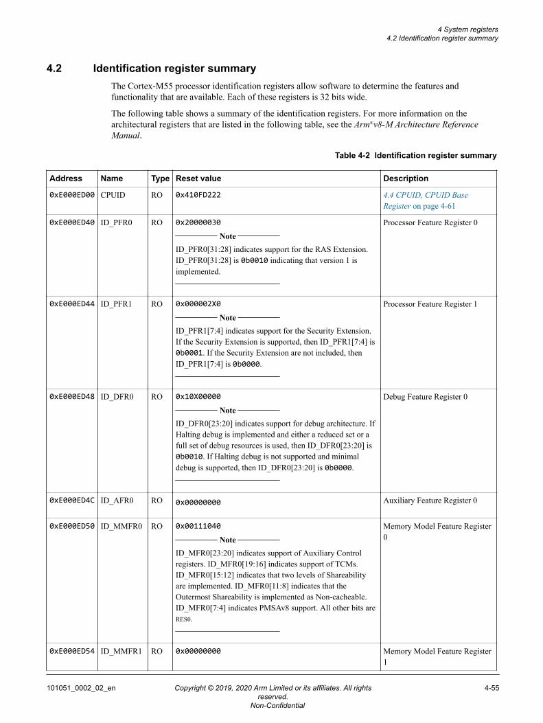
4.2 Identification register summaryThe Cortex-M55 processor identification registers allow software to determine the features andfunctionality that are available. Each of these registers is 32 bits wide.
The following table shows a summary of the identification registers. For more information on thearchitectural registers that are listed in the following table, see the Arm®v8-M Architecture ReferenceManual.
Table 4-2 Identification register summary
Address Name Type Reset value Description
0xE000ED00 CPUID RO 0x410FD222 4.4 CPUID, CPUID BaseRegister on page 4-61
0xE000ED40 ID_PFR0 RO 0x20000030 Note
ID_PFR0[31:28] indicates support for the RAS Extension.ID_PFR0[31:28] is 0b0010 indicating that version 1 isimplemented.
Processor Feature Register 0
0xE000ED44 ID_PFR1 RO 0x000002X0 Note
ID_PFR1[7:4] indicates support for the Security Extension.If the Security Extension is supported, then ID_PFR1[7:4] is0b0001. If the Security Extension are not included, thenID_PFR1[7:4] is 0b0000.
Processor Feature Register 1
0xE000ED48 ID_DFR0 RO 0x10X00000 Note
ID_DFR0[23:20] indicates support for debug architecture. IfHalting debug is implemented and either a reduced set or afull set of debug resources is used, then ID_DFR0[23:20] is0b0010. If Halting debug is not supported and minimaldebug is supported, then ID_DFR0[23:20] is 0b0000.
Debug Feature Register 0
0xE000ED4C ID_AFR0 RO 0x00000000 Auxiliary Feature Register 0
0xE000ED50 ID_MMFR0 RO 0x00111040 Note
ID_MFR0[23:20] indicates support of Auxiliary Controlregisters. ID_MFR0[19:16] indicates support of TCMs.ID_MFR0[15:12] indicates that two levels of Shareabilityare implemented. ID_MFR0[11:8] indicates that theOutermost Shareability is implemented as Non-cacheable.ID_MFR0[7:4] indicates PMSAv8 support. All other bits areRES0.
Memory Model Feature Register0
0xE000ED54 ID_MMFR1 RO 0x00000000 Memory Model Feature Register1
4 System registers4.2 Identification register summary
101051_0002_02_en Copyright © 2019, 2020 Arm Limited or its affiliates. All rightsreserved.
4-55
Non-Confidential
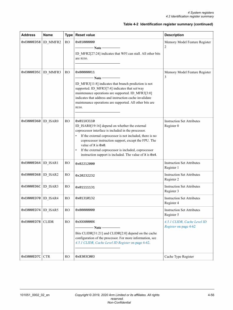
Table 4-2 Identification register summary (continued)
Address Name Type Reset value Description
0xE000ED58 ID_MMFR2 RO 0x01000000 Note
ID_MFR2[27:24] indicates that WFI can stall. All other bitsare RES0.
Memory Model Feature Register2
0xE000ED5C ID_MMFR3 RO 0x00000011 Note
ID_MFR3[11:8] indicates that branch prediction is notsupported. ID_MFR3[7:4] indicates that set/waymaintenance operations are supported. ID_MFR3[3:0]indicates that address and instruction cache invalidatemaintenance operations are supported. All other bits areRES0.
Memory Model Feature Register3
0xE000ED60 ID_ISAR0 RO 0x011X3110ID_ISAR0[19:16] depend on whether the externalcoprocessor interface is included in the processor.• If the external coprocessor is not included, there is no
coprocessor instruction support, except the FPU. Thevalue of X is 0x0.
• If the external coprocessor is included, coprocessorinstruction support is included. The value of X is 0x4.
Instruction Set AttributesRegister 0
0xE000ED64 ID_ISAR1 RO 0x02212000 Instruction Set AttributesRegister 1
0xE000ED68 ID_ISAR2 RO 0x20232232 Instruction Set AttributesRegister 2
0xE000ED6C ID_ISAR3 RO 0x01111131 Instruction Set AttributesRegister 3
0xE000ED70 ID_ISAR4 RO 0x01310132 Instruction Set AttributesRegister 4
0xE000ED74 ID_ISAR5 RO 0x00000000 Instruction Set AttributesRegister 5
0xE000ED78 CLIDR RO 0xXXX0000X Note
Bits CLIDR[31:21] and CLIDR[2:0] depend on the cacheconfiguration of the processor. For more information, see4.5.1 CLIDR, Cache Level ID Register on page 4-62.
4.5.1 CLIDR, Cache Level IDRegister on page 4-62
0xE000ED7C CTR RO 0x8303C003 Cache Type Register
4 System registers4.2 Identification register summary
101051_0002_02_en Copyright © 2019, 2020 Arm Limited or its affiliates. All rightsreserved.
4-56
Non-Confidential
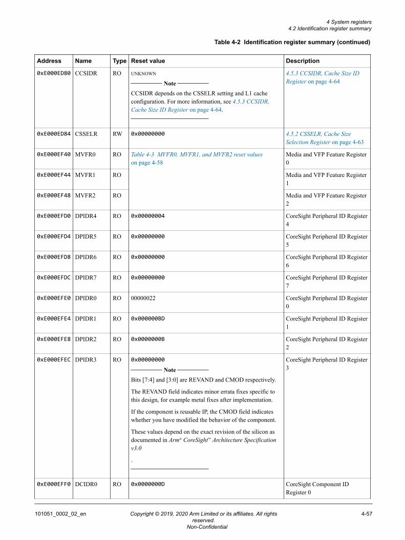
Table 4-2 Identification register summary (continued)
Address Name Type Reset value Description
0xE000ED80 CCSIDR RO UNKNOWN
Note
CCSIDR depends on the CSSELR setting and L1 cacheconfiguration. For more information, see 4.5.3 CCSIDR,Cache Size ID Register on page 4-64.
4.5.3 CCSIDR, Cache Size IDRegister on page 4-64
0xE000ED84 CSSELR RW 0x00000000 4.5.2 CSSELR, Cache SizeSelection Register on page 4-63
0xE000EF40 MVFR0 RO Table 4-3 MVFR0, MVFR1, and MVFR2 reset valueson page 4-58
Media and VFP Feature Register0
0xE000EF44 MVFR1 RO Media and VFP Feature Register1
0xE000EF48 MVFR2 RO Media and VFP Feature Register2
0xE000EFD0 DPIDR4 RO 0x00000004 CoreSight Peripheral ID Register4
0xE000EFD4 DPIDR5 RO 0x00000000 CoreSight Peripheral ID Register5
0xE000EFD8 DPIDR6 RO 0x00000000 CoreSight Peripheral ID Register6
0xE000EFDC DPIDR7 RO 0x00000000 CoreSight Peripheral ID Register7
0xE000EFE0 DPIDR0 RO 00000022 CoreSight Peripheral ID Register0
0xE000EFE4 DPIDR1 RO 0x000000BD CoreSight Peripheral ID Register1
0xE000EFE8 DPIDR2 RO 0x0000000B CoreSight Peripheral ID Register2
0xE000EFEC DPIDR3 RO 0x00000000 Note
Bits [7:4] and [3:0] are REVAND and CMOD respectively.
The REVAND field indicates minor errata fixes specific tothis design, for example metal fixes after implementation.
If the component is reusable IP, the CMOD field indicateswhether you have modified the behavior of the component.
These values depend on the exact revision of the silicon asdocumented in Arm® CoreSight™ Architecture Specificationv3.0
.
CoreSight Peripheral ID Register3
0xE000EFF0 DCIDR0 RO 0x0000000D CoreSight Component IDRegister 0
4 System registers4.2 Identification register summary
101051_0002_02_en Copyright © 2019, 2020 Arm Limited or its affiliates. All rightsreserved.
4-57
Non-Confidential
Table 4-2 Identification register summary (continued)
Address Name Type Reset value Description
0xE000EFF4 DCIDR1 RO 0x00000090 CoreSight Component IDRegister 1
0xE000EFF8 DCIDR2 RO 0x00000005 CoreSight Component IDRegister 2
0xE000EFFC DCIDR3 RO 0x000000B1 CoreSight Component IDRegister 3
0xE000EFBC DDEVARCH RO 0x47702A04 CoreSight Device ArchitectureRegister
0xE000ECFC REVIDR RO 0x00000000 Revision ID register
0xE0005FC8 ERRDEVID RO 0x00000001 Note
ERRDEVID[15:0] indicates the number of error records thatthe RAS Extension implementation supports. In the Cortex-M55 processor, this field reads 0x0001 indicating one errorrecord is supported.
This register is RAZ if any of the following conditions aretrue:• ECC protection is not configured.• ECC protection is configured but not enabled
Error Record Device ID Register.See 10.5.6 ERRDEVID, RASError Record Device ID Registeron page 10-229.
4.2.1 Media and VFP Feature Register reset values, MVFR0, MVFR1, and MVFR2 reset values
The MVFR0, MVFR1, and MVFR2 register reset values depend on the M‑profile Vector Extension(MVE) and floating-point functionality configuration. The MVE and floating-point functionalityoperation is configured using the MVE and FPU configuration parameters.
For more information, see 2.6 Cortex®-M55 implementation options on page 2-39.
The following table shows the MVFR0, MVFR1, and MVFR2 reset values based on the resetconfigurations.
Table 4-3 MVFR0, MVFR1, and MVFR2 reset values
Configuration MVFR0 MVFR1 MVFR2
MVE=0, FPU=0 0x00000000 0x00000000 0x00000000
MVE=1, FPU=0 0x00000001 0x00000100 0x00000000
MVE=0, FPU=1 0x10110221 0x12100011 0x00000040
MVE=1, FPU=1 0x10110221 0x12100111 0x00000040
MVE=2, FPU=1 0x10110221 0x12100211 0x00000040
4 System registers4.2 Identification register summary
101051_0002_02_en Copyright © 2019, 2020 Arm Limited or its affiliates. All rightsreserved.
4-58
Non-Confidential
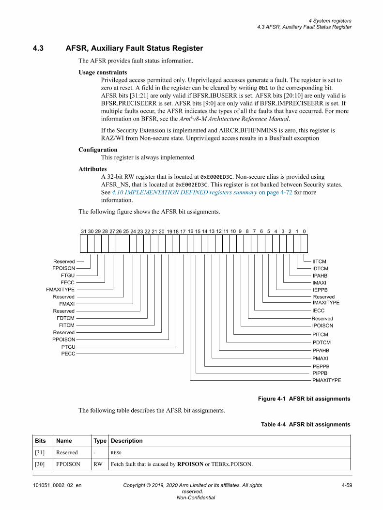
4.3 AFSR, Auxiliary Fault Status RegisterThe AFSR provides fault status information.
Usage constraintsPrivileged access permitted only. Unprivileged accesses generate a fault. The register is set tozero at reset. A field in the register can be cleared by writing 0b1 to the corresponding bit.AFSR bits [31:21] are only valid if BFSR.IBUSERR is set. AFSR bits [20:10] are only valid isBFSR.PRECISEERR is set. AFSR bits [9:0] are only valid if BFSR.IMPRECISEERR is set. Ifmultiple faults occur, the AFSR indicates the types of all the faults that have occurred. For moreinformation on BFSR, see the Arm®v8-M Architecture Reference Manual.
If the Security Extension is implemented and AIRCR.BFHFNMINS is zero, this register isRAZ/WI from Non-secure state. Unprivileged access results in a BusFault exception
ConfigurationThis register is always implemented.
AttributesA 32-bit RW register that is located at 0xE000ED3C. Non-secure alias is provided usingAFSR_NS, that is located at 0xE002ED3C. This register is not banked between Security states.See 4.10 IMPLEMENTATION DEFINED registers summary on page 4-72 for moreinformation.
The following figure shows the AFSR bit assignments.
31 16 15 4 3 0282930 14 13 12 11 10 9 8 7 6 5 2 1
ReservedFPOISON
27 26
FTGUFECC
FMAXITYPE
25
Reserved
24
FMAXI
23
Reserved
22
FDTCM
21
FITCM
20
Reserved
19
PPOISON
18
PTGU
17
PECC
IITCMIDTCMIPAHBIMAXIIEPPB
IMAXITYPEIECCReserved
PITCMPDTCMPPAHBPMAXIPEPPB
PMAXITYPE
Reserved
PIPPB
IPOISON
Figure 4-1 AFSR bit assignments
The following table describes the AFSR bit assignments.
Table 4-4 AFSR bit assignments
Bits Name Type Description
[31] Reserved - RES0
[30] FPOISON RW Fetch fault that is caused by RPOISON or TEBRx.POISON.
4 System registers4.3 AFSR, Auxiliary Fault Status Register
101051_0002_02_en Copyright © 2019, 2020 Arm Limited or its affiliates. All rightsreserved.
4-59
Non-Confidential
Table 4-4 AFSR bit assignments (continued)
Bits Name Type Description
[29] FTGU - Fetch fault that is caused by TCM Gate Unit (TGU) security violation.
[28] FECC RW Fetch fault that is caused by uncorrectable Error Correcting Code (ECC) error.
[27] FMAXITYPE RW AXI response that caused the fetch fault. Only valid when AFSR.FMAXI is 1.
0b0 SLVERR
0b1 DECERR
[26:25] Reserved - RES0
[24] FMAXI RW Fetch fault on Master AXI (M-AXI) interface.
[23] Reserved - RES0
[22] FDTCM RW Fetch fault on Data Tightly Coupled Memory (DTCM) interface.
[21] FITCM RW Fetch fault on Instruction Tightly Coupled Memory (ITCM) interface.
[20] Reserved - RES0
[19] PPOISON RW Precise fault that is caused by RPOISON or TEBRx.POISON.
[18] PTGU RW Precise fault that is caused by TGU security violation.
[17] PECC RW Precise fault that is caused by uncorrectable ECC error.
[16] PMAXITYPE RW AXI response that caused the precise fault. Only valid when AFSR.PMAXI is 1.
0b0 SLVERR
0b1 DECERR
[15] PIPPB RW Precise fault on Internal Private Peripheral Bus (IPPB) interface.
[14] PEPPB RW Precise fault on External Private Peripheral Bus (EPPB) interface.
[13] PMAXI RW Precise fault on M-AXI interface.
[12] PPAHB RW Precise fault on Peripheral AHB (P-AHB) interface.
[11] PDTCM RW Precise fault on DTCM interface.
[10] PITCM RW Precise fault on ITCM interface.
[9] IPOISON RW Imprecise BusFault because of RPOISON.
[8] Reserved - RES0
[7] IECC RW Imprecise fault that is caused by uncorrectable ECC error.
[6] IMAXITYPE RW AXI response that caused the imprecise fault. Only valid when AFSR.IMAXI is 1.
0b0 SLVERR
0b1 DECERR
[5] Reserved - RES0
[4] IEPPB RW Imprecise fault on EPPB interface.
[3] IMAXI RW Imprecise fault on M-AXI interface.
[2] IPAHB RW Imprecise fault on P-AHB interface.
[1] IDTCM RW Imprecise fault on DTCM interface.
[0] IITCM RW Imprecise fault on ITCM interface.
4 System registers4.3 AFSR, Auxiliary Fault Status Register
101051_0002_02_en Copyright © 2019, 2020 Arm Limited or its affiliates. All rightsreserved.
4-60
Non-Confidential
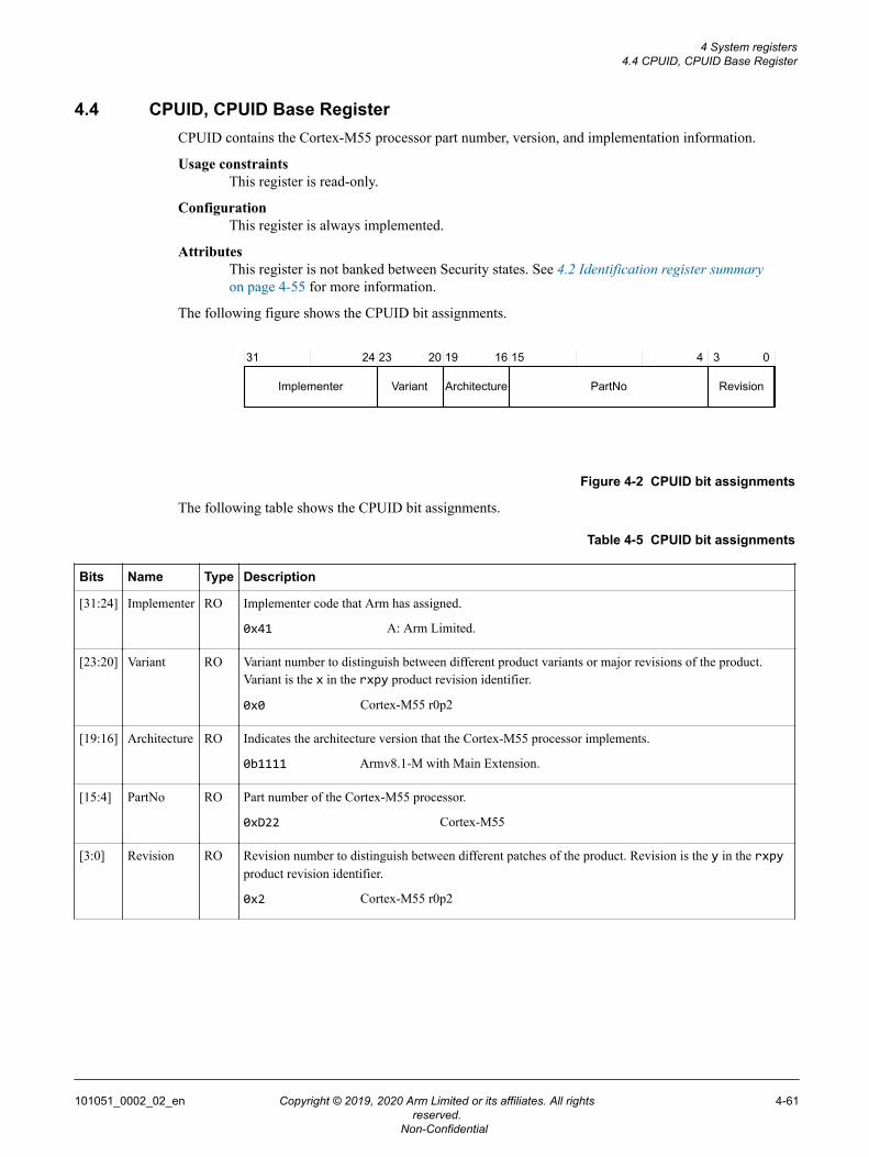
4.4 CPUID, CPUID Base RegisterCPUID contains the Cortex-M55 processor part number, version, and implementation information.
Usage constraintsThis register is read-only.
ConfigurationThis register is always implemented.
AttributesThis register is not banked between Security states. See 4.2 Identification register summaryon page 4-55 for more information.
The following figure shows the CPUID bit assignments.
Revision
31 24 23 20 19 16 15 4 3 0
PartNoArchitectureVariantImplementer
Figure 4-2 CPUID bit assignments
The following table shows the CPUID bit assignments.
Table 4-5 CPUID bit assignments
Bits Name Type Description
[31:24] Implementer RO Implementer code that Arm has assigned.
0x41 A: Arm Limited.
[23:20] Variant RO Variant number to distinguish between different product variants or major revisions of the product.Variant is the x in the rxpy product revision identifier.
0x0 Cortex-M55 r0p2
[19:16] Architecture RO Indicates the architecture version that the Cortex-M55 processor implements.
0b1111 Armv8.1‑M with Main Extension.
[15:4] PartNo RO Part number of the Cortex-M55 processor.
0xD22 Cortex-M55
[3:0] Revision RO Revision number to distinguish between different patches of the product. Revision is the y in the rxpyproduct revision identifier.
0x2 Cortex-M55 r0p2
4 System registers4.4 CPUID, CPUID Base Register
101051_0002_02_en Copyright © 2019, 2020 Arm Limited or its affiliates. All rightsreserved.
4-61
Non-Confidential
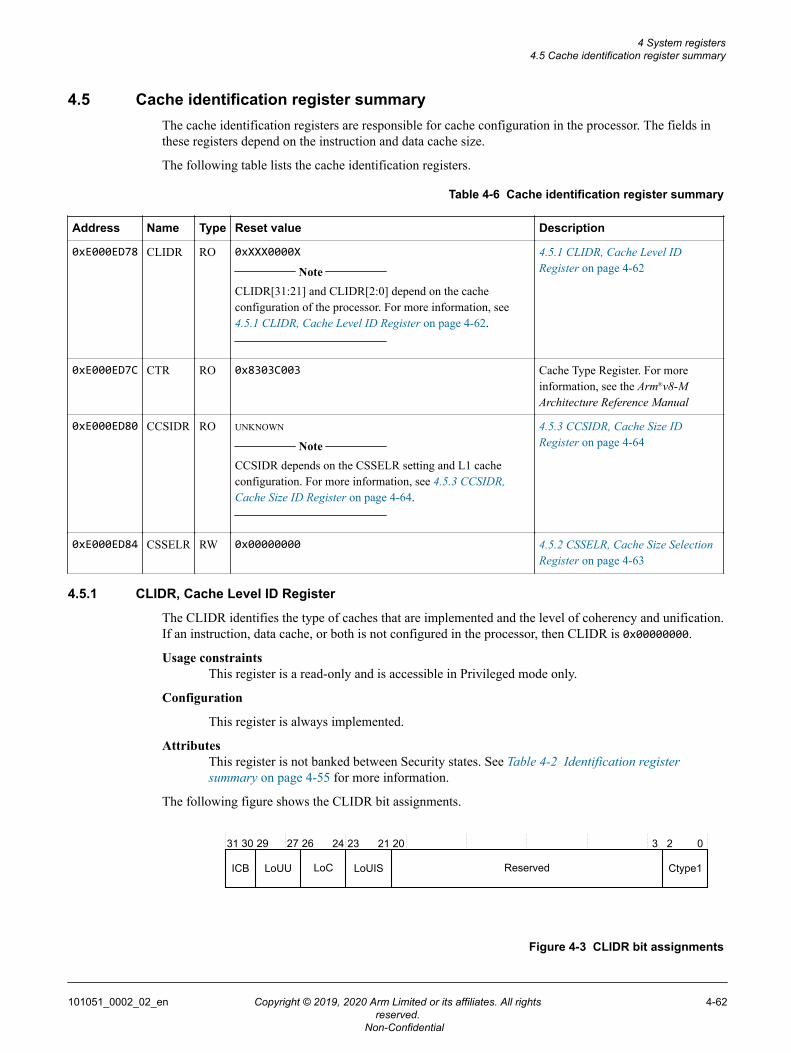
4.5 Cache identification register summaryThe cache identification registers are responsible for cache configuration in the processor. The fields inthese registers depend on the instruction and data cache size.
The following table lists the cache identification registers.
Table 4-6 Cache identification register summary
Address Name Type Reset value Description
0xE000ED78 CLIDR RO 0xXXX0000X Note
CLIDR[31:21] and CLIDR[2:0] depend on the cacheconfiguration of the processor. For more information, see4.5.1 CLIDR, Cache Level ID Register on page 4-62.
4.5.1 CLIDR, Cache Level IDRegister on page 4-62
0xE000ED7C CTR RO 0x8303C003 Cache Type Register. For moreinformation, see the Arm®v8-MArchitecture Reference Manual
0xE000ED80 CCSIDR RO UNKNOWN
Note
CCSIDR depends on the CSSELR setting and L1 cacheconfiguration. For more information, see 4.5.3 CCSIDR,Cache Size ID Register on page 4-64.
4.5.3 CCSIDR, Cache Size IDRegister on page 4-64
0xE000ED84 CSSELR RW 0x00000000 4.5.2 CSSELR, Cache Size SelectionRegister on page 4-63
4.5.1 CLIDR, Cache Level ID Register
The CLIDR identifies the type of caches that are implemented and the level of coherency and unification.If an instruction, data cache, or both is not configured in the processor, then CLIDR is 0x00000000.
Usage constraintsThis register is a read-only and is accessible in Privileged mode only.
Configuration
This register is always implemented.
AttributesThis register is not banked between Security states. See Table 4-2 Identification registersummary on page 4-55 for more information.
The following figure shows the CLIDR bit assignments.
31 3 024 23 2026272930 2
LoUU LoC LoUIS Reserved Ctype1ICB
21
Figure 4-3 CLIDR bit assignments
4 System registers4.5 Cache identification register summary
101051_0002_02_en Copyright © 2019, 2020 Arm Limited or its affiliates. All rightsreserved.
4-62
Non-Confidential
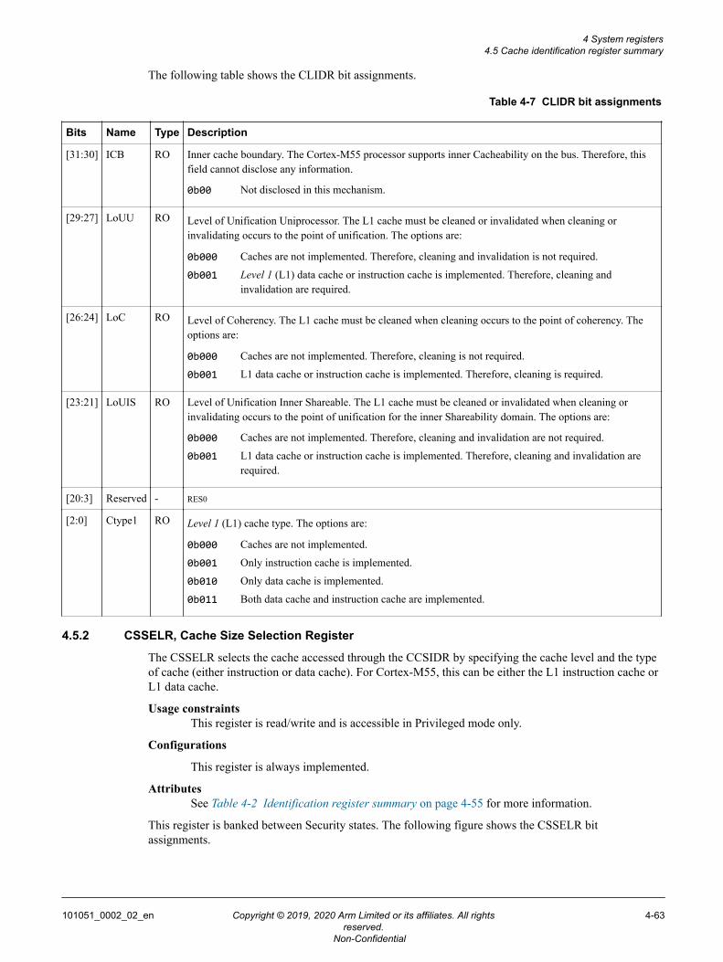
The following table shows the CLIDR bit assignments.
Table 4-7 CLIDR bit assignments
Bits Name Type Description
[31:30] ICB RO Inner cache boundary. The Cortex-M55 processor supports inner Cacheability on the bus. Therefore, thisfield cannot disclose any information.
0b00 Not disclosed in this mechanism.
[29:27] LoUU RO Level of Unification Uniprocessor. The L1 cache must be cleaned or invalidated when cleaning orinvalidating occurs to the point of unification. The options are:
0b000 Caches are not implemented. Therefore, cleaning and invalidation is not required.
0b001 Level 1 (L1) data cache or instruction cache is implemented. Therefore, cleaning andinvalidation are required.
[26:24] LoC RO Level of Coherency. The L1 cache must be cleaned when cleaning occurs to the point of coherency. Theoptions are:
0b000 Caches are not implemented. Therefore, cleaning is not required.
0b001 L1 data cache or instruction cache is implemented. Therefore, cleaning is required.
[23:21] LoUIS RO Level of Unification Inner Shareable. The L1 cache must be cleaned or invalidated when cleaning orinvalidating occurs to the point of unification for the inner Shareability domain. The options are:
0b000 Caches are not implemented. Therefore, cleaning and invalidation are not required.
0b001 L1 data cache or instruction cache is implemented. Therefore, cleaning and invalidation arerequired.
[20:3] Reserved - RES0
[2:0] Ctype1 RO Level 1 (L1) cache type. The options are:
0b000 Caches are not implemented.
0b001 Only instruction cache is implemented.
0b010 Only data cache is implemented.
0b011 Both data cache and instruction cache are implemented.
4.5.2 CSSELR, Cache Size Selection Register
The CSSELR selects the cache accessed through the CCSIDR by specifying the cache level and the typeof cache (either instruction or data cache). For Cortex-M55, this can be either the L1 instruction cache orL1 data cache.
Usage constraintsThis register is read/write and is accessible in Privileged mode only.
Configurations
This register is always implemented.
AttributesSee Table 4-2 Identification register summary on page 4-55 for more information.
This register is banked between Security states. The following figure shows the CSSELR bitassignments.
4 System registers4.5 Cache identification register summary
101051_0002_02_en Copyright © 2019, 2020 Arm Limited or its affiliates. All rightsreserved.
4-63
Non-Confidential
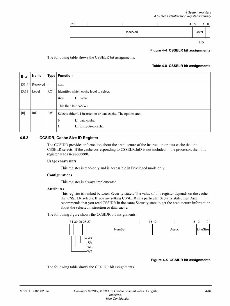
Reserved Level
4 3 1 0
InD
31
Figure 4-4 CSSELR bit assignments
The following table shows the CSSELR bit assignments.
Table 4-8 CSSELR bit assignments
Bits Name Type Function
[31:4] Reserved - RES0
[3:1] Level RO Identifies which cache level to select.
0x0 L1 cache.
This field is RAZ/WI.
[0] InD RW Selects either L1 instruction or data cache. The options are:
0 L1 data cache.
1 L1 instruction cache.
4.5.3 CCSIDR, Cache Size ID Register
The CCSIDR provides information about the architecture of the instruction or data cache that theCSSELR selects. If the cache corresponding to CSSELR.InD is not included in the processor, then thisregister reads 0x00000000.
Usage constraints
This register is read-only and is accessible in Privileged mode only.
Configurations
This register is always implemented.
AttributesThis register is banked between Security states. The value of this register depends on the cachethat CSSELR selects. If you are setting CSSELR in a particular Security state, then Armrecommends that you read CSSIDR in the same Security state to get the architecture informationabout the selected instruction or data cache.
The following figure shows the CCSIDR bit assignments.
AssocNumSet LineSize
31 3 2 030 29 28
RAWA
WB
121327
WT
Figure 4-5 CCSIDR bit assignments
The following table shows the CCSIDR bit assignments.
4 System registers4.5 Cache identification register summary
101051_0002_02_en Copyright © 2019, 2020 Arm Limited or its affiliates. All rightsreserved.
4-64
Non-Confidential
Table 4-9 CCSIDR bit assignments
Bits Name Type Function
[31] WT RO Indicates support available for Write-Through:
0b1 Write-Through support available.
[30] WB RO Indicates support available for Write-Back:
0b1 Write-Back support available.
[29] RA RO Indicates support available for read allocation:
0b1 Read allocation support available.
[28] WA RO Indicates support available for write allocation:
0b1 Write allocation support available.
[27:13] NumSet RO Indicates the number of sets.
Cache-size dependent.
[12:3] Assoc RO Indicates associativity. The value depends on the cache that CSSELR selects.
When CSSELR.InD=1 (L1 instruction cache):
0x1 2-way set associative instruction cache.
When CSSELR.InD=0 (L1 data cache):
0x3 4-way set associative data cache.
[2:0] LineSize RO Indicates the number of words in each cache line.
0b1 Represents 32 bytes.
The LineSize field is encoded as 2 less than log(2) of the number of words in the cache line. Forexample, a value of 0x0 indicates that there are four words in a cache line, that is the minimum size forthe cache. A value of 0x1 indicates that there are eight words in a cache line.
4 System registers4.5 Cache identification register summary
101051_0002_02_en Copyright © 2019, 2020 Arm Limited or its affiliates. All rightsreserved.
4-65
Non-Confidential
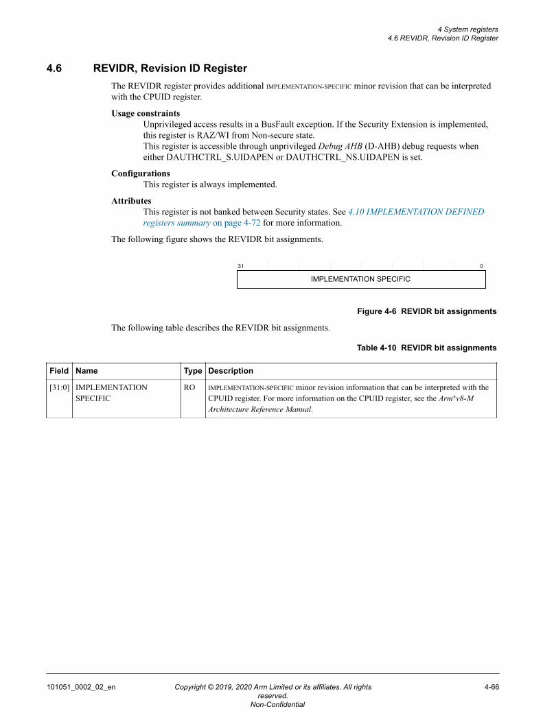
4.6 REVIDR, Revision ID RegisterThe REVIDR register provides additional IMPLEMENTATION-SPECIFIC minor revision that can be interpretedwith the CPUID register.
Usage constraintsUnprivileged access results in a BusFault exception. If the Security Extension is implemented,this register is RAZ/WI from Non-secure state.This register is accessible through unprivileged Debug AHB (D-AHB) debug requests wheneither DAUTHCTRL_S.UIDAPEN or DAUTHCTRL_NS.UIDAPEN is set.
ConfigurationsThis register is always implemented.
AttributesThis register is not banked between Security states. See 4.10 IMPLEMENTATION DEFINEDregisters summary on page 4-72 for more information.
The following figure shows the REVIDR bit assignments.
31 0
IMPLEMENTATION SPECIFIC
Figure 4-6 REVIDR bit assignments
The following table describes the REVIDR bit assignments.
Table 4-10 REVIDR bit assignments
Field Name Type Description
[31:0] IMPLEMENTATIONSPECIFIC
RO IMPLEMENTATION-SPECIFIC minor revision information that can be interpreted with theCPUID register. For more information on the CPUID register, see the Arm®v8-MArchitecture Reference Manual.
4 System registers4.6 REVIDR, Revision ID Register
101051_0002_02_en Copyright © 2019, 2020 Arm Limited or its affiliates. All rightsreserved.
4-66
Non-Confidential
4.7 Implementation control register summaryImplementation control registers are architecturally defined with values that control aspects of systemimplementation.
The following table shows a summary of the implementation control registers. For more information onthe architectural registers that are listed in the following table, see the Arm®v8-M Architecture ReferenceManual.
Table 4-11 Implementation control register summary
Address Name Type Reset value Description
0xE000E004 ICTR RO 0x0000000X Note
ICTR[3:0] depends on the number of interrupts that areincluded in the processor. Bits [31:4] are zero.
4.9 ICTR, Interrupt Controller TypeRegister on page 4-71
0xE000E008 ACTLR RW 0x00000000 4.8 ACTLR, Auxiliary Control Registeron page 4-68
0xE000E00C CPPWR RW 0x00000000 Coprocessor Power Control Register
4 System registers4.7 Implementation control register summary
101051_0002_02_en Copyright © 2019, 2020 Arm Limited or its affiliates. All rightsreserved.
4-67
Non-Confidential
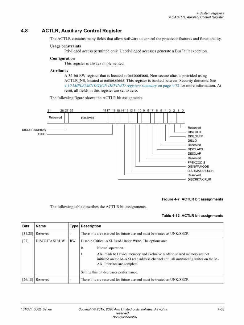
4.8 ACTLR, Auxiliary Control RegisterThe ACTLR contains many fields that allow software to control the processor features and functionality.
Usage constraintsPrivileged access permitted only. Unprivileged accesses generate a BusFault exception.
ConfigurationThis register is always implemented.
AttributesA 32-bit RW register that is located at 0xE000E008. Non-secure alias is provided usingACTLR_NS, located at 0xE002E008. This register is banked between Security domains. See4.10 IMPLEMENTATION DEFINED registers summary on page 4-72 for more information. Atreset, all fields in this register are set to zero.
The following figure shows the ACTLR bit assignments.
31 16 15 4 3 028 14 13 12 11 10 9 8 7 6 5 2 1
Reserved
ReservedDISITMATBFLUSH
ReservedDISFOLD
FPEXCODISDISNWAMODE
DISLOReservedDISOLAPSDISOLAPReserved
DISCRITAXIRUR
1727
DISCRITAXIRUW
26
Reserved
18
DISDIDISLOLEP
Figure 4-7 ACTLR bit assignments
The following table describes the ACTLR bit assignments.
Table 4-12 ACTLR bit assignments
Bits Name Type Description
[31:28] Reserved - These bits are reserved for future use and must be treated as UNK/SBZP.
[27] DISCRITAXIRUW RW Disable-Critical-AXI-Read-Under-Write. The options are:
0 Normal operation.
1 AXI reads to Device memory and exclusive reads to shared memory are notinitiated on the M-AXI read address channel until all outstanding writes on the M-AXI interface are complete.
Setting this bit decreases performance.
[26:18] Reserved - These bits are reserved for future use and must be treated as UNK/SBZP.
4 System registers4.8 ACTLR, Auxiliary Control Register
101051_0002_02_en Copyright © 2019, 2020 Arm Limited or its affiliates. All rightsreserved.
4-68
Non-Confidential
Table 4-12 ACTLR bit assignments (continued)
Bits Name Type Description
[17:16] DISDI RW Disable dual-issue features. The options for this bit are:
0b00 Full dual-issue, if DISFOLD is set to 0.
0b01 Disable dual-issue of arithmetic instructions.
0b10 Disable lane swapping
0b11 Disable dual-issue of arithmetic instructions and lane swapping.
[15] DISCRITAXIRUR RW Disable critical AXI Read-Under-Read. The options for this bit are:
0 Normal operation.
1 AXI reads to Device memory and exclusive reads to shared memory are notinitiated on the M-AXI read address channels if there are any outstanding reads onthe M-AXI. Transactions on the M-AXI cannot be interrupted.
This bit might reduce the time that these transactions are in progress and might improve worst-case interrupt latency. Setting this bit reduces performance.
[14:13] Reserved - These bits are reserved for future use and must be treated as UNK/SBZP.
[12] DISITMATBFLUSH RW This bit determines whether Instrumentation Trace Macrocell (ITM) or Data Watchpoint andTrace (DWT) ATB flush is disabled. The options for this bit are:
0 Normal operation.
1 ITM or DWT ATB flush is disabled.
When disabled, the AFVALID signal (trace flush request) is ignored and the AFREADY(trace flush ready) signal is held HIGH. This field only resets on Cold reset.
[11] DISNWAMODE RW This bit determines if no write allocate mode is disabled. The options for this bit are:
0 Normal operation.
1 No write allocate mode is disabled.
Setting this bit decreases performance. For more information on no write allocation mode, seeNo Write-Allocate mode on page 9-197.
[10] FPEXCODIS RW This bit determines if floating-point exception outputs are disabled. The options for this bit are:
0 Normal operation.
1 Floating-point exception outputs are disabled.
[9:8] Reserved - These bits are reserved for future use and must be treated as UNK/SBZP.
[7] DISOLAP RW Disable overlapping of all instructions.
[6] DISOLAPS RW Disable overlapping of scalar-only instructions.
[5] Reserved - UNK/SBZP
[4] DISLO RW Disable low overhead loops. The options are:
0 Low overhead loops enabled.
1 Low overhead loops disabled.
4 System registers4.8 ACTLR, Auxiliary Control Register
101051_0002_02_en Copyright © 2019, 2020 Arm Limited or its affiliates. All rightsreserved.
4-69
Non-Confidential
Table 4-12 ACTLR bit assignments (continued)
Bits Name Type Description
[3] DISLOLEP RW Disable end of loop prediction in for low overhead loops.
The options are:
0 Low overhead loop end prediction enabled
1 Low overhead loop end prediction disabled
Setting this bit decreases performance.
[2] DISFOLD RW This bit determines if dual-issue functionality is disabled. The options are:
0 Normal operation.
1 Dual-issue functionality is disabled.
Setting this bit decreases performance.
[1:0] Reserved - These bits are reserved for future use and must be treated as UNK/SBZP.
4 System registers4.8 ACTLR, Auxiliary Control Register
101051_0002_02_en Copyright © 2019, 2020 Arm Limited or its affiliates. All rightsreserved.
4-70
Non-Confidential
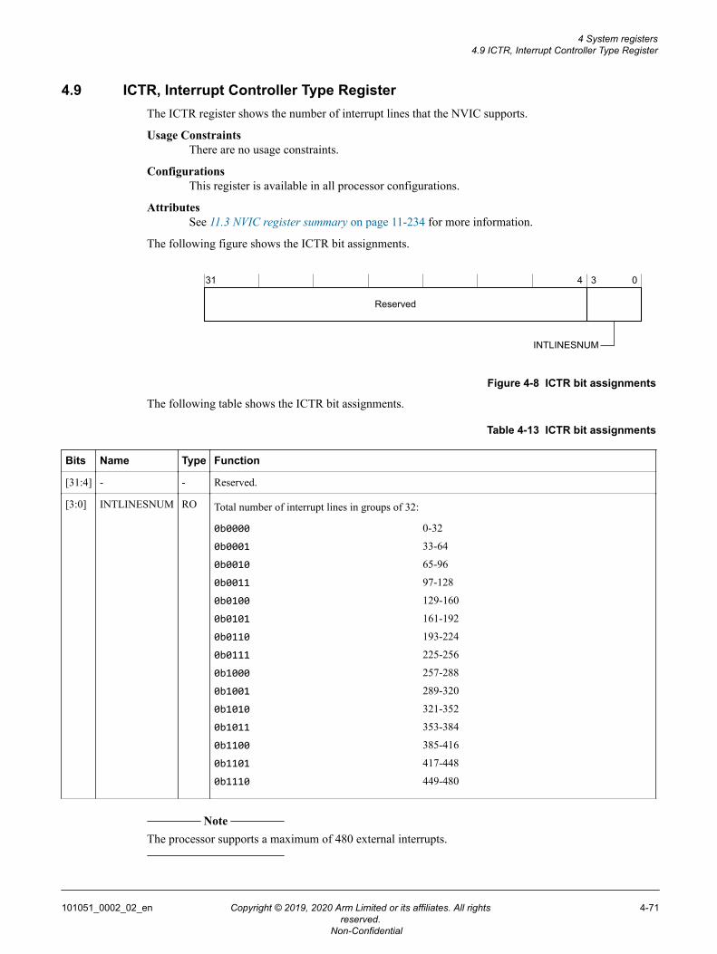
4.9 ICTR, Interrupt Controller Type RegisterThe ICTR register shows the number of interrupt lines that the NVIC supports.
Usage ConstraintsThere are no usage constraints.
ConfigurationsThis register is available in all processor configurations.
AttributesSee 11.3 NVIC register summary on page 11-234 for more information.
The following figure shows the ICTR bit assignments.
Reserved
31 4 3 0
INTLINESNUM
Figure 4-8 ICTR bit assignments
The following table shows the ICTR bit assignments.
Table 4-13 ICTR bit assignments
Bits Name Type Function
[31:4] - - Reserved.
[3:0] INTLINESNUM RO Total number of interrupt lines in groups of 32:
0b0000 0-32
0b0001 33-64
0b0010 65-96
0b0011 97-128
0b0100 129-160
0b0101 161-192
0b0110 193-224
0b0111 225-256
0b1000 257-288
0b1001 289-320
0b1010 321-352
0b1011 353-384
0b1100 385-416
0b1101 417-448
0b1110 449-480
Note
The processor supports a maximum of 480 external interrupts.
4 System registers4.9 ICTR, Interrupt Controller Type Register
101051_0002_02_en Copyright © 2019, 2020 Arm Limited or its affiliates. All rightsreserved.
4-71
Non-Confidential
4.10 IMPLEMENTATION DEFINED registers summaryThe 32-bit IMPLEMENTATION DEFINED registers provide memory configuration and access control, errorrecord information, interrupt control, and processor configuration information.
The following table lists the IMPLEMENTATION DEFINED registers for the Cortex-M55 processor.
Table 4-14 IMPLEMENTATION DEFINED registers summary
Address Name Type Reset value Description
0xE0005000 ERRFR0 RO 0x00000101 10.5.1 ERRFR0, RAS Error Record FeatureRegister on page 10-223
0xE0005008 ERRCTRL0 - - This register is RES0.
0xE0005010 ERRSTATUS0 RW 0xXXX000XX 10.5.2 ERRSTATUS0, RAS Error Record PrimaryStatus Register on page 10-223
0xE0005018 ERRADDR0 RO 0xXXXXXXXX 10.5.3 ERRADDR0 and ERRADDR20, RAS ErrorRecord Address Registers on page 10-225
0xE000501C ERRADDR20 RO 0xX0000000 10.5.3 ERRADDR0 and ERRADDR20, RAS ErrorRecord Address Registers on page 10-225
0xE0005020 ERRMISC00 - - This register is RES0.
0xE0005024 ERRMISC10 RO 0x0000000X 10.5.4 ERRMISC10, Error Record MiscellaneousRegister 10 on page 10-227
0xE0005028 ERRMISC20 - - This register is RES0.
0xE000502C ERRMISC30 - - This register is RES0.
0xE0005030 ERRMISC40 - - This register is RES0.
0xE0005034 ERRMISC50 - - This register is RES0.
0xE0005038 ERRMISC60 - - This register is RES0.
0xE000503C ERRMISC70 - - This register is RES0.
0xE0005E00 ERRGSR0 RO 0x00000000 10.5.5 ERRGSR0, RAS Fault Group StatusRegister on page 10-228
0xE000ECFC REVIDR RO 0x00000000 4.6 REVIDR, Revision ID Register on page 4-66
0xE0005FC8 ERRDEVID RO 0x00000001 10.5.6 ERRDEVID, RAS Error Record Device IDRegister on page 10-229
0xE000E008 ACTLR RW 0x00000000 4.8 ACTLR, Auxiliary Control Registeron page 4-68
0xE000ED3C AFSR RW 0x00000000 4.3 AFSR, Auxiliary Fault Status Registeron page 4-59
0xE000EF04 RFSR RW 0xXXXX000X 10.5.7 RFSR, RAS Fault Status Registeron page 10-229
4 System registers4.10 IMPLEMENTATION DEFINED registers summary
101051_0002_02_en Copyright © 2019, 2020 Arm Limited or its affiliates. All rightsreserved.
4-72
Non-Confidential
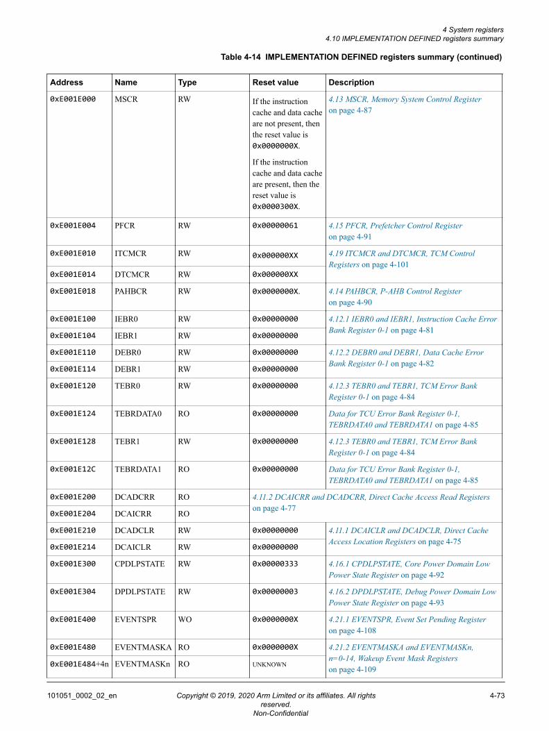
Table 4-14 IMPLEMENTATION DEFINED registers summary (continued)
Address Name Type Reset value Description
0xE001E000 MSCR RW If the instructioncache and data cacheare not present, thenthe reset value is0x0000000X.
If the instructioncache and data cacheare present, then thereset value is0x0000300X.
4.13 MSCR, Memory System Control Registeron page 4-87
0xE001E004 PFCR RW 0x00000061 4.15 PFCR, Prefetcher Control Registeron page 4-91
0xE001E010 ITCMCR RW 0x000000XX 4.19 ITCMCR and DTCMCR, TCM ControlRegisters on page 4-101
0xE001E014 DTCMCR RW 0x000000XX
0xE001E018 PAHBCR RW 0x0000000X. 4.14 PAHBCR, P-AHB Control Registeron page 4-90
0xE001E100 IEBR0 RW 0x00000000 4.12.1 IEBR0 and IEBR1, Instruction Cache ErrorBank Register 0-1 on page 4-81
0xE001E104 IEBR1 RW 0x00000000
0xE001E110 DEBR0 RW 0x00000000 4.12.2 DEBR0 and DEBR1, Data Cache ErrorBank Register 0-1 on page 4-82
0xE001E114 DEBR1 RW 0x00000000
0xE001E120 TEBR0 RW 0x00000000 4.12.3 TEBR0 and TEBR1, TCM Error BankRegister 0-1 on page 4-84
0xE001E124 TEBRDATA0 RO 0x00000000 Data for TCU Error Bank Register 0-1,TEBRDATA0 and TEBRDATA1 on page 4-85
0xE001E128 TEBR1 RW 0x00000000 4.12.3 TEBR0 and TEBR1, TCM Error BankRegister 0-1 on page 4-84
0xE001E12C TEBRDATA1 RO 0x00000000 Data for TCU Error Bank Register 0-1,TEBRDATA0 and TEBRDATA1 on page 4-85
0xE001E200 DCADCRR RO 4.11.2 DCAICRR and DCADCRR, Direct Cache Access Read Registerson page 4-77
0xE001E204 DCAICRR RO
0xE001E210 DCADCLR RW 0x00000000 4.11.1 DCAICLR and DCADCLR, Direct CacheAccess Location Registers on page 4-75
0xE001E214 DCAICLR RW 0x00000000
0xE001E300 CPDLPSTATE RW 0x00000333 4.16.1 CPDLPSTATE, Core Power Domain LowPower State Register on page 4-92
0xE001E304 DPDLPSTATE RW 0x00000003 4.16.2 DPDLPSTATE, Debug Power Domain LowPower State Register on page 4-93
0xE001E400 EVENTSPR WO 0x0000000X 4.21.1 EVENTSPR, Event Set Pending Registeron page 4-108
0xE001E480 EVENTMASKA RO 0x0000000X 4.21.2 EVENTMASKA and EVENTMASKn,n=0-14, Wakeup Event Mask Registerson page 4-1090xE001E484+4n EVENTMASKn RO UNKNOWN
4 System registers4.10 IMPLEMENTATION DEFINED registers summary
101051_0002_02_en Copyright © 2019, 2020 Arm Limited or its affiliates. All rightsreserved.
4-73
Non-Confidential
Table 4-14 IMPLEMENTATION DEFINED registers summary (continued)
Address Name Type Reset value Description
0xE001E500 ITGU_CTRL RW 0x00000003 4.20.1 ITGU_CTRL and DTGU_CTRL, ITGU andDTGU Control Registers on page 4-103
0xE001E504 ITGU_CFG RO 0xX0002X0X 4.20.2 ITGU_CFG and DTGU_CFG, ITGU andDTGU Configuration Registers on page 4-104
0xE001E510+4n ITGU_LUTn • RW if 32n+1<2Number of
ITGU blocks
• RO if 32n+1≥2Number of
ITGU blocks
0x00000000 4.20.3 ITGU_LUTn and DTGU_LUTn, ITGU andDTGU Look Up Table Registers on page 4-105
0xE001E600 DTGU_CTRL RW 0x00000003 4.20.1 ITGU_CTRL and DTGU_CTRL, ITGU andDTGU Control Registers on page 4-103
0xE001E604 DTGU_CFG RO 0xX0002X0X 4.20.2 ITGU_CFG and DTGU_CFG, ITGU andDTGU Configuration Registers on page 4-104
0xE001E610+4n DTGU_LUTn • RW if 32n+1<2Number of
DTGU blocks
• RO if 32n+1≥2Number of
DTGU blocks
0x00000000 4.20.3 ITGU_LUTn and DTGU_LUTn, ITGU andDTGU Look Up Table Registers on page 4-105
0xE001E700 CFGINFOSEL WO UNKNOWN 4.17.1 CFGINFOSEL, Processor configurationinformation selection register on page 4-95
0xE001E704 CFGINFORD RO UNKNOWN 4.17.2 CFGINFORD, Processor configurationinformation read data register on page 4-98
Note
The following registers are reset on Cold reset only. These reset values persist across a system reset orWarm reset.• 10.5.1 ERRFR0, RAS Error Record Feature Register on page 10-223.• 10.5.4 ERRMISC10, Error Record Miscellaneous Register 10 on page 10-227.• 10.5.3 ERRADDR0 and ERRADDR20, RAS Error Record Address Registers on page 10-225.• 10.5.2 ERRSTATUS0, RAS Error Record Primary Status Register on page 10-223.• 10.5.5 ERRGSR0, RAS Fault Group Status Register on page 10-228.
4 System registers4.10 IMPLEMENTATION DEFINED registers summary
101051_0002_02_en Copyright © 2019, 2020 Arm Limited or its affiliates. All rightsreserved.
4-74
Non-Confidential
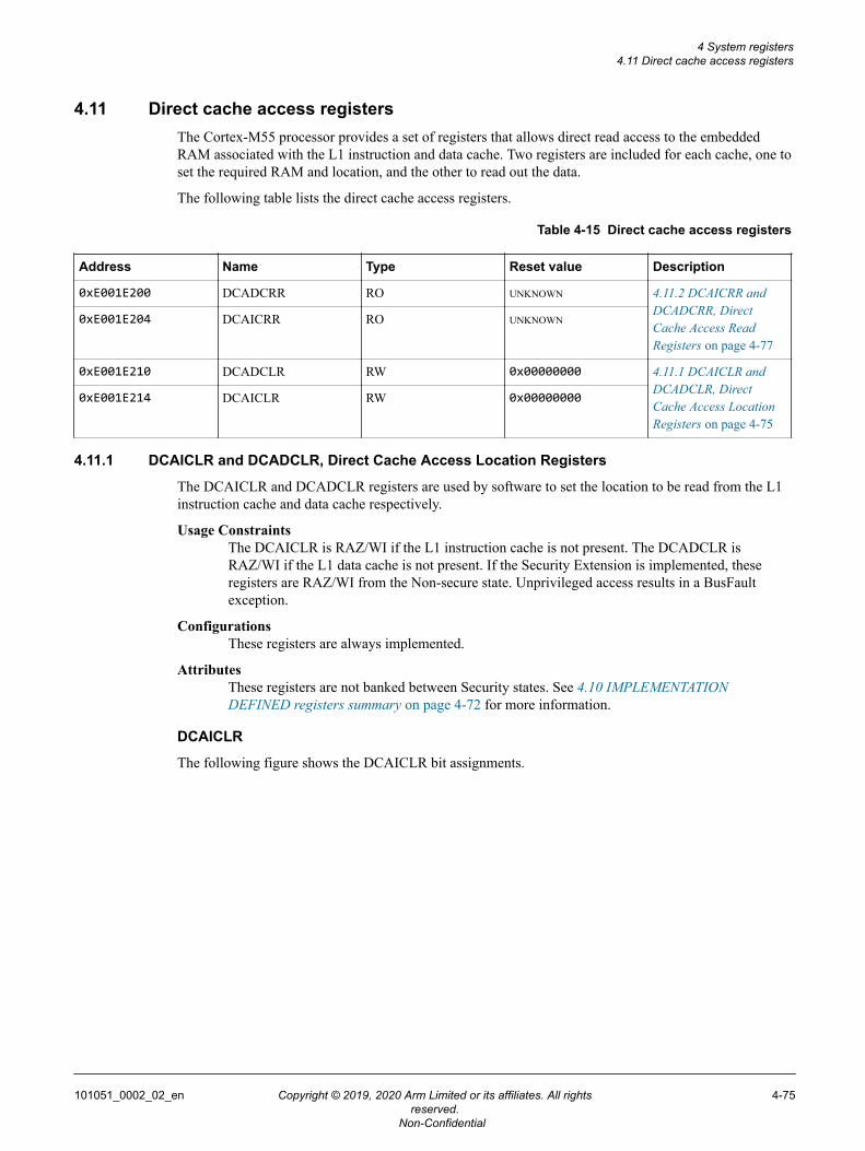
4.11 Direct cache access registersThe Cortex-M55 processor provides a set of registers that allows direct read access to the embeddedRAM associated with the L1 instruction and data cache. Two registers are included for each cache, one toset the required RAM and location, and the other to read out the data.
The following table lists the direct cache access registers.
Table 4-15 Direct cache access registers
Address Name Type Reset value Description
0xE001E200 DCADCRR RO UNKNOWN 4.11.2 DCAICRR andDCADCRR, DirectCache Access ReadRegisters on page 4-77
0xE001E204 DCAICRR RO UNKNOWN
0xE001E210 DCADCLR RW 0x00000000 4.11.1 DCAICLR andDCADCLR, DirectCache Access LocationRegisters on page 4-75
0xE001E214 DCAICLR RW 0x00000000
4.11.1 DCAICLR and DCADCLR, Direct Cache Access Location Registers
The DCAICLR and DCADCLR registers are used by software to set the location to be read from the L1instruction cache and data cache respectively.
Usage ConstraintsThe DCAICLR is RAZ/WI if the L1 instruction cache is not present. The DCADCLR isRAZ/WI if the L1 data cache is not present. If the Security Extension is implemented, theseregisters are RAZ/WI from the Non-secure state. Unprivileged access results in a BusFaultexception.
ConfigurationsThese registers are always implemented.
AttributesThese registers are not banked between Security states. See 4.10 IMPLEMENTATIONDEFINED registers summary on page 4-72 for more information.
DCAICLR
The following figure shows the DCAICLR bit assignments.
4 System registers4.11 Direct cache access registers
101051_0002_02_en Copyright © 2019, 2020 Arm Limited or its affiliates. All rightsreserved.
4-75
Non-Confidential
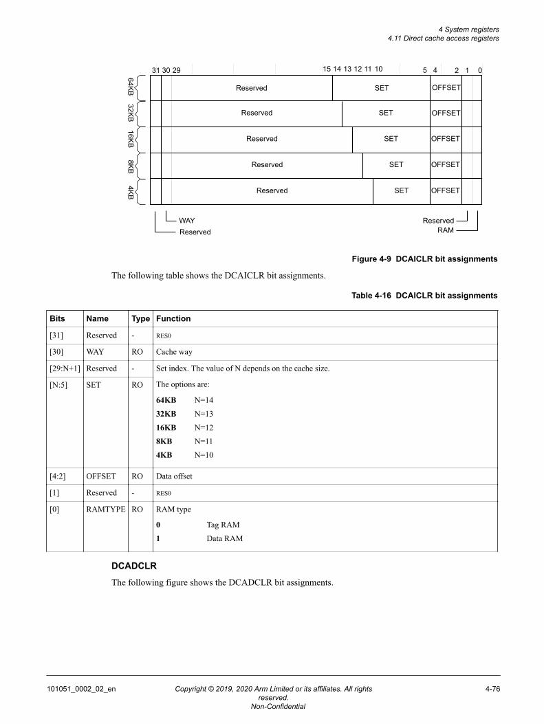
31 02930 5 4 1
WAY
Reserved SET OFFSET
2
ReservedRAMReserved
OFFSET
OFFSET
OFFSET
OFFSET
SET
SET
SET
SET
15 14 13 12 11 10
Reserved
Reserved
Reserved
Reserved
64KB
32KB
16KB
8KB
4KB
Figure 4-9 DCAICLR bit assignments
The following table shows the DCAICLR bit assignments.
Table 4-16 DCAICLR bit assignments
Bits Name Type Function
[31] Reserved - RES0
[30] WAY RO Cache way
[29:N+1] Reserved - Set index. The value of N depends on the cache size.
The options are:
64KB N=14
32KB N=13
16KB N=12
8KB N=11
4KB N=10
[N:5] SET RO
[4:2] OFFSET RO Data offset
[1] Reserved - RES0
[0] RAMTYPE RO RAM type
0 Tag RAM
1 Data RAM
DCADCLR
The following figure shows the DCADCLR bit assignments.
4 System registers4.11 Direct cache access registers
101051_0002_02_en Copyright © 2019, 2020 Arm Limited or its affiliates. All rightsreserved.
4-76
Non-Confidential
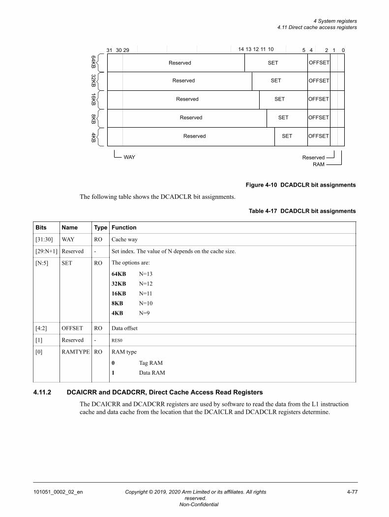
31 02930 5 4 1
WAY
Reserved SET OFFSET
2
ReservedRAM
OFFSET
OFFSET
OFFSET
OFFSET
SET
SET
SET
SET
14 13 12 11 10
Reserved
Reserved
Reserved
Reserved
64KB
32KB
16KB
8KB
4KB
Figure 4-10 DCADCLR bit assignments
The following table shows the DCADCLR bit assignments.
Table 4-17 DCADCLR bit assignments
Bits Name Type Function
[31:30] WAY RO Cache way
[29:N+1] Reserved - Set index. The value of N depends on the cache size.
The options are:
64KB N=13
32KB N=12
16KB N=11
8KB N=10
4KB N=9
[N:5] SET RO
[4:2] OFFSET RO Data offset
[1] Reserved - RES0
[0] RAMTYPE RO RAM type
0 Tag RAM
1 Data RAM
4.11.2 DCAICRR and DCADCRR, Direct Cache Access Read Registers
The DCAICRR and DCADCRR registers are used by software to read the data from the L1 instructioncache and data cache from the location that the DCAICLR and DCADCLR registers determine.
4 System registers4.11 Direct cache access registers
101051_0002_02_en Copyright © 2019, 2020 Arm Limited or its affiliates. All rightsreserved.
4-77
Non-Confidential
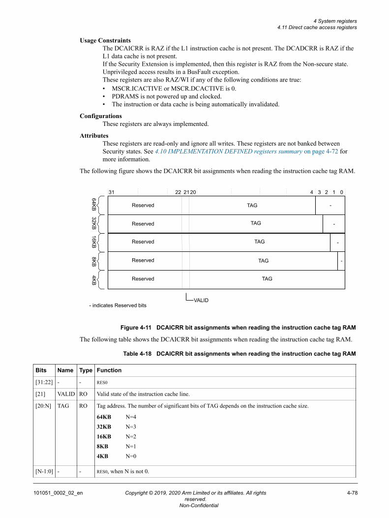
Usage ConstraintsThe DCAICRR is RAZ if the L1 instruction cache is not present. The DCADCRR is RAZ if theL1 data cache is not present.If the Security Extension is implemented, then this register is RAZ from the Non-secure state.Unprivileged access results in a BusFault exception.These registers are also RAZ/WI if any of the following conditions are true:• MSCR.ICACTIVE or MSCR.DCACTIVE is 0.• PDRAMS is not powered up and clocked.• The instruction or data cache is being automatically invalidated.
ConfigurationsThese registers are always implemented.
AttributesThese registers are read-only and ignore all writes. These registers are not banked betweenSecurity states. See 4.10 IMPLEMENTATION DEFINED registers summary on page 4-72 formore information.
The following figure shows the DCAICRR bit assignments when reading the instruction cache tag RAM.
31 04
VALID
Reserved TAG -
TAG
TAG
TAG
TAG
Reserved
Reserved
Reserved
Reserved
64KB
32KB
16KB
8KB
4KB
22 2120 3 2 1
-
-
-
- indicates Reserved bits
Figure 4-11 DCAICRR bit assignments when reading the instruction cache tag RAM
The following table shows the DCAICRR bit assignments when reading the instruction cache tag RAM.
Table 4-18 DCAICRR bit assignments when reading the instruction cache tag RAM
Bits Name Type Function
[31:22] - - RES0
[21] VALID RO Valid state of the instruction cache line.
[20:N] TAG RO Tag address. The number of significant bits of TAG depends on the instruction cache size.
64KB N=4
32KB N=3
16KB N=2
8KB N=1
4KB N=0
[N-1:0] - - RES0, when N is not 0.
4 System registers4.11 Direct cache access registers
101051_0002_02_en Copyright © 2019, 2020 Arm Limited or its affiliates. All rightsreserved.
4-78
Non-Confidential
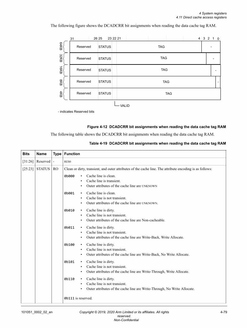
The following figure shows the DCADCRR bit assignments when reading the data cache tag RAM.
31 04
VALID
Reserved TAG -
TAG
TAG
TAG
Reserved
Reserved
Reserved
Reserved
64KB
32KB
16KB
8KB
4KB
23 22 21 3 2 1
-
-
-
- indicates Reserved bits
25
STATUS
TAG
26
STATUS
STATUS
STATUS
STATUS
Figure 4-12 DCADCRR bit assignments when reading the data cache tag RAM
The following table shows the DCADCRR bit assignments when reading the data cache tag RAM.
Table 4-19 DCADCRR bit assignments when reading the data cache tag RAM
Bits Name Type Function
[31:26] Reserved - RES0
[25:23] STATUS RO Clean or dirty, transient, and outer attributes of the cache line. The attribute encoding is as follows:
0b000 • Cache line is clean.• Cache line is transient.• Outer attributes of the cache line are UNKNOWN
0b001 • Cache line is clean.• Cache line is not transient.• Outer attributes of the cache line are UNKNOWN.
0b010 • Cache line is dirty.• Cache line is not transient.• Outer attributes of the cache line are Non-cacheable.
0b011 • Cache line is dirty.• Cache line is not transient.• Outer attributes of the cache line are Write-Back, Write Allocate.
0b100 • Cache line is dirty.• Cache line is not transient.• Outer attributes of the cache line are Write-Back, No Write Allocate.
0b101 • Cache line is dirty.• Cache line is not transient.• Outer attributes of the cache line are Write-Through, Write Allocate.
0b110 • Cache line is dirty.• Cache line is not transient.• Outer attributes of the cache line are Write-Through, No Write Allocate.
0b111 is reserved.
4 System registers4.11 Direct cache access registers
101051_0002_02_en Copyright © 2019, 2020 Arm Limited or its affiliates. All rightsreserved.
4-79
Non-Confidential
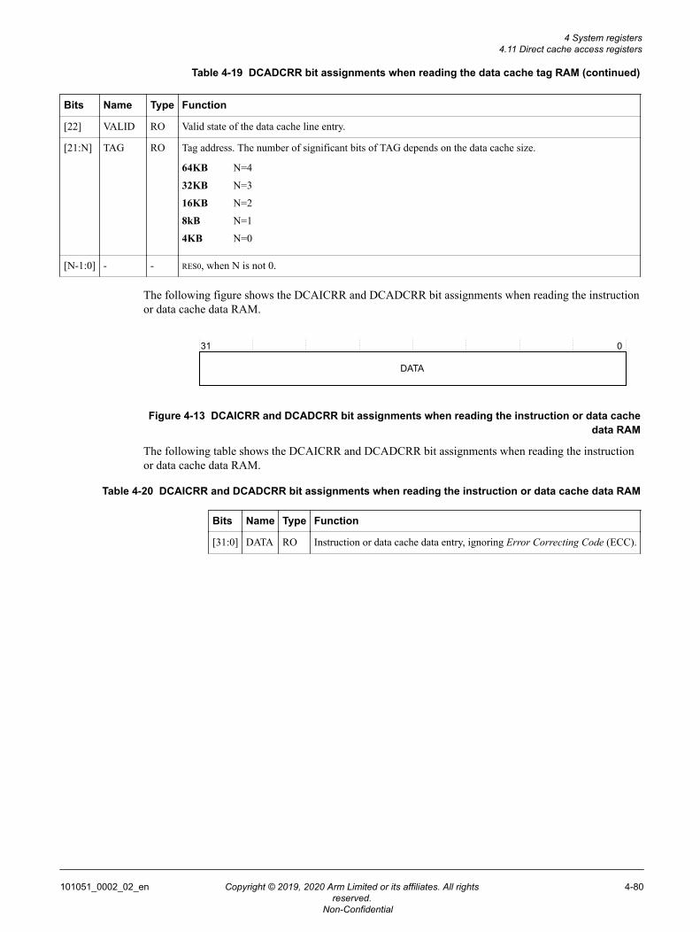
Table 4-19 DCADCRR bit assignments when reading the data cache tag RAM (continued)
Bits Name Type Function
[22] VALID RO Valid state of the data cache line entry.
[21:N] TAG RO Tag address. The number of significant bits of TAG depends on the data cache size.
64KB N=4
32KB N=3
16KB N=2
8kB N=1
4KB N=0
[N-1:0] - - RES0, when N is not 0.
The following figure shows the DCAICRR and DCADCRR bit assignments when reading the instructionor data cache data RAM.
31 0
DATA
Figure 4-13 DCAICRR and DCADCRR bit assignments when reading the instruction or data cachedata RAM
The following table shows the DCAICRR and DCADCRR bit assignments when reading the instructionor data cache data RAM.
Table 4-20 DCAICRR and DCADCRR bit assignments when reading the instruction or data cache data RAM
Bits Name Type Function
[31:0] DATA RO Instruction or data cache data entry, ignoring Error Correcting Code (ECC).
4 System registers4.11 Direct cache access registers
101051_0002_02_en Copyright © 2019, 2020 Arm Limited or its affiliates. All rightsreserved.
4-80
Non-Confidential
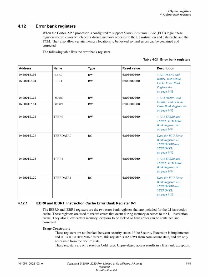
4.12 Error bank registersWhen the Cortex-M55 processor is configured to support Error Correcting Code (ECC) logic, theseregisters record errors which occur during memory accesses to the L1 instruction and data cache and theTCM. They also allow certain memory locations to be locked so hard errors can be contained andcorrected.
The following table lists the error bank registers.
Table 4-21 Error bank registers
Address Name Type Reset value Description
0xE001E100 IEBR0 RW 0x00000000 4.12.1 IEBR0 andIEBR1, InstructionCache Error BankRegister 0-1on page 4-81
0xE001E104 IEBR1 RW 0x00000000
0xE001E110 DEBR0 RW 0x00000000 4.12.2 DEBR0 andDEBR1, Data CacheError Bank Register 0-1on page 4-82
0xE001E114 DEBR1 RW 0x00000000
0xE001E120 TEBR0 RW 0x00000000 4.12.3 TEBR0 andTEBR1, TCM ErrorBank Register 0-1on page 4-84
0xE001E124 TEBRDATA0 RO 0x00000000 Data for TCU ErrorBank Register 0-1,TEBRDATA0 andTEBRDATA1on page 4-85
0xE001E128 TEBR1 RW 0x00000000 4.12.3 TEBR0 andTEBR1, TCM ErrorBank Register 0-1on page 4-84
0xE001E12C TEBRDATA1 RO 0x00000000 Data for TCU ErrorBank Register 0-1,TEBRDATA0 andTEBRDATA1on page 4-85
4.12.1 IEBR0 and IEBR1, Instruction Cache Error Bank Register 0-1
The IEBR0 and IEBR1 registers are the two error bank registers that are included for the L1 instructioncache. These registers are used to record errors that occur during memory accesses to the L1 instructioncache. They also allow certain memory locations to be locked so hard errors can be contained andcorrected.
Usage ConstraintsThese registers are not banked between security states. If the Security Extension is implementedand AIRCR.BFHFNMINS is zero, this register is RAZ/WI from Non-secure state, and are onlyaccessible from the Secure state.These registers are only reset on Cold reset. Unprivileged access results in a BusFault exception.
4 System registers4.12 Error bank registers
101051_0002_02_en Copyright © 2019, 2020 Arm Limited or its affiliates. All rightsreserved.
4-81
Non-Confidential
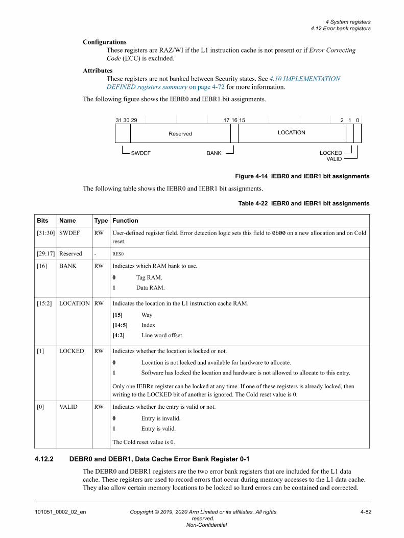
ConfigurationsThese registers are RAZ/WI if the L1 instruction cache is not present or if Error CorrectingCode (ECC) is excluded.
AttributesThese registers are not banked between Security states. See 4.10 IMPLEMENTATIONDEFINED registers summary on page 4-72 for more information.
The following figure shows the IEBR0 and IEBR1 bit assignments.
31 16 15 02930 17 2 1
LOCKEDVALID
LOCATION
BANK
Reserved
SWDEF
Figure 4-14 IEBR0 and IEBR1 bit assignments
The following table shows the IEBR0 and IEBR1 bit assignments.
Table 4-22 IEBR0 and IEBR1 bit assignments
Bits Name Type Function
[31:30] SWDEF RW User-defined register field. Error detection logic sets this field to 0b00 on a new allocation and on Coldreset.
[29:17] Reserved - RES0
[16] BANK RW Indicates which RAM bank to use.
0 Tag RAM.
1 Data RAM.
[15:2] LOCATION RW Indicates the location in the L1 instruction cache RAM.
[15] Way
[14:5] Index
[4:2] Line word offset.
[1] LOCKED RW Indicates whether the location is locked or not.
0 Location is not locked and available for hardware to allocate.
1 Software has locked the location and hardware is not allowed to allocate to this entry.
Only one IEBRn register can be locked at any time. If one of these registers is already locked, thenwriting to the LOCKED bit of another is ignored. The Cold reset value is 0.
[0] VALID RW Indicates whether the entry is valid or not.
0 Entry is invalid.
1 Entry is valid.
The Cold reset value is 0.
4.12.2 DEBR0 and DEBR1, Data Cache Error Bank Register 0-1
The DEBR0 and DEBR1 registers are the two error bank registers that are included for the L1 datacache. These registers are used to record errors that occur during memory accesses to the L1 data cache.They also allow certain memory locations to be locked so hard errors can be contained and corrected.
4 System registers4.12 Error bank registers
101051_0002_02_en Copyright © 2019, 2020 Arm Limited or its affiliates. All rightsreserved.
4-82
Non-Confidential
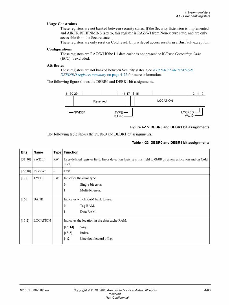
Usage ConstraintsThese registers are not banked between security states. If the Security Extension is implementedand AIRCR.BFHFNMINS is zero, this register is RAZ/WI from Non-secure state, and are onlyaccessible from the Secure state.These registers are only reset on Cold reset. Unprivileged access results in a BusFault exception.
ConfigurationsThese registers are RAZ/WI if the L1 data cache is not present or if Error Correcting Code(ECC) is excluded.
AttributesThese registers are not banked between Security states. See 4.10 IMPLEMENTATIONDEFINED registers summary on page 4-72 for more information.
The following figure shows the DEBR0 and DEBR1 bit assignments.
31 16 15 02930 17 2 1
LOCKEDVALID
LOCATION
BANK
Reserved
SWDEF
18
TYPE
Figure 4-15 DEBR0 and DEBR1 bit assignments
The following table shows the DEBR0 and DEBR1 bit assignments.
Table 4-23 DEBR0 and DEBR1 bit assignments
Bits Name Type Function
[31:30] SWDEF RW User-defined register field. Error detection logic sets this field to 0b00 on a new allocation and on Coldreset.
[29:18] Reserved - RES0
[17] TYPE RW Indicates the error type.
0 Single-bit error.
1 Multi-bit error.
[16] BANK Indicates which RAM bank to use.
0 Tag RAM.
1 Data RAM.
[15:2] LOCATION Indicates the location in the data cache RAM.
[15:14] Way.
[13:5] Index.
[4:2] Line doubleword offset.
4 System registers4.12 Error bank registers
101051_0002_02_en Copyright © 2019, 2020 Arm Limited or its affiliates. All rightsreserved.
4-83
Non-Confidential
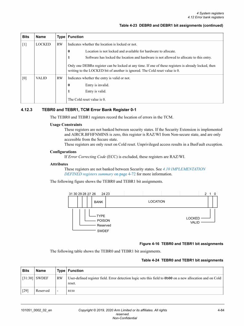
Table 4-23 DEBR0 and DEBR1 bit assignments (continued)
Bits Name Type Function
[1] LOCKED RW Indicates whether the location is locked or not.
0 Location is not locked and available for hardware to allocate.
1 Software has locked the location and hardware is not allowed to allocate to this entry.
Only one DEBRn register can be locked at any time. If one of these registers is already locked, thenwriting to the LOCKED bit of another is ignored. The Cold reset value is 0.
[0] VALID RW Indicates whether the entry is valid or not.
0 Entry is invalid.
1 Entry is valid.
The Cold reset value is 0.
4.12.3 TEBR0 and TEBR1, TCM Error Bank Register 0-1
The TEBR0 and TEBR1 registers record the location of errors in the TCM.
Usage ConstraintsThese registers are not banked between security states. If the Security Extension is implementedand AIRCR.BFHFNMINS is zero, this register is RAZ/WI from Non-secure state, and are onlyaccessible from the Secure state.These registers are only reset on Cold reset. Unprivileged access results in a BusFault exception.
ConfigurationsIf Error Correcting Code (ECC) is excluded, these registers are RAZ/WI.
AttributesThese registers are not banked between Security states. See 4.10 IMPLEMENTATIONDEFINED registers summary on page 4-72 for more information.
The following figure shows the TEBR0 and TEBR1 bit assignments.
31 02930 2 1
LOCKEDVALID
LOCATIONBANK
POISONReserved
SWDEF
28 27 26 24 23
TYPE
Figure 4-16 TEBR0 and TEBR1 bit assignments
The following table shows the TEBR0 and TEBR1 bit assignments.
Table 4-24 TEBR0 and TEBR1 bit assignments
Bits Name Type Function
[31:30] SWDEF RW User-defined register field. Error detection logic sets this field to 0b00 on a new allocation and on Coldreset.
[29] Reserved - RES0
4 System registers4.12 Error bank registers
101051_0002_02_en Copyright © 2019, 2020 Arm Limited or its affiliates. All rightsreserved.
4-84
Non-Confidential
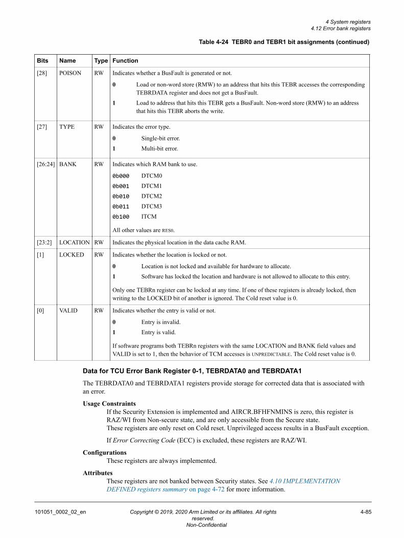
Table 4-24 TEBR0 and TEBR1 bit assignments (continued)
Bits Name Type Function
[28] POISON RW Indicates whether a BusFault is generated or not.
0 Load or non-word store (RMW) to an address that hits this TEBR accesses the correspondingTEBRDATA register and does not get a BusFault.
1 Load to address that hits this TEBR gets a BusFault. Non-word store (RMW) to an addressthat hits this TEBR aborts the write.
[27] TYPE RW Indicates the error type.
0 Single-bit error.
1 Multi-bit error.
[26:24] BANK RW Indicates which RAM bank to use.
0b000 DTCM0
0b001 DTCM1
0b010 DTCM2
0b011 DTCM3
0b100 ITCM
All other values are RES0.
[23:2] LOCATION RW Indicates the physical location in the data cache RAM.
[1] LOCKED RW Indicates whether the location is locked or not.
0 Location is not locked and available for hardware to allocate.
1 Software has locked the location and hardware is not allowed to allocate to this entry.
Only one TEBRn register can be locked at any time. If one of these registers is already locked, thenwriting to the LOCKED bit of another is ignored. The Cold reset value is 0.
[0] VALID RW Indicates whether the entry is valid or not.
0 Entry is invalid.
1 Entry is valid.
If software programs both TEBRn registers with the same LOCATION and BANK field values andVALID is set to 1, then the behavior of TCM accesses is UNPREDICTABLE. The Cold reset value is 0.
Data for TCU Error Bank Register 0-1, TEBRDATA0 and TEBRDATA1
The TEBRDATA0 and TEBRDATA1 registers provide storage for corrected data that is associated withan error.
Usage ConstraintsIf the Security Extension is implemented and AIRCR.BFHFNMINS is zero, this register isRAZ/WI from Non-secure state, and are only accessible from the Secure state.These registers are only reset on Cold reset. Unprivileged access results in a BusFault exception.
If Error Correcting Code (ECC) is excluded, these registers are RAZ/WI.
ConfigurationsThese registers are always implemented.
AttributesThese registers are not banked between Security states. See 4.10 IMPLEMENTATIONDEFINED registers summary on page 4-72 for more information.
4 System registers4.12 Error bank registers
101051_0002_02_en Copyright © 2019, 2020 Arm Limited or its affiliates. All rightsreserved.
4-85
Non-Confidential
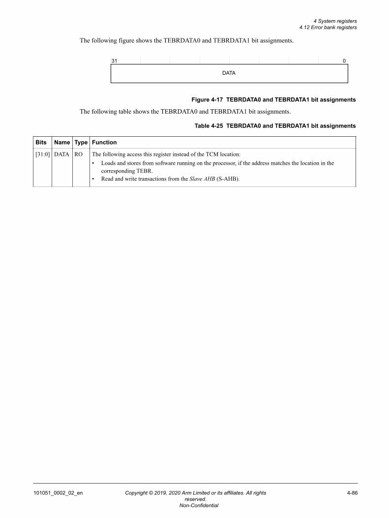
The following figure shows the TEBRDATA0 and TEBRDATA1 bit assignments.
31 0
DATA
Figure 4-17 TEBRDATA0 and TEBRDATA1 bit assignments
The following table shows the TEBRDATA0 and TEBRDATA1 bit assignments.
Table 4-25 TEBRDATA0 and TEBRDATA1 bit assignments
Bits Name Type Function
[31:0] DATA RO The following access this register instead of the TCM location:• Loads and stores from software running on the processor, if the address matches the location in the
corresponding TEBR.• Read and write transactions from the Slave AHB (S-AHB).
4 System registers4.12 Error bank registers
101051_0002_02_en Copyright © 2019, 2020 Arm Limited or its affiliates. All rightsreserved.
4-86
Non-Confidential
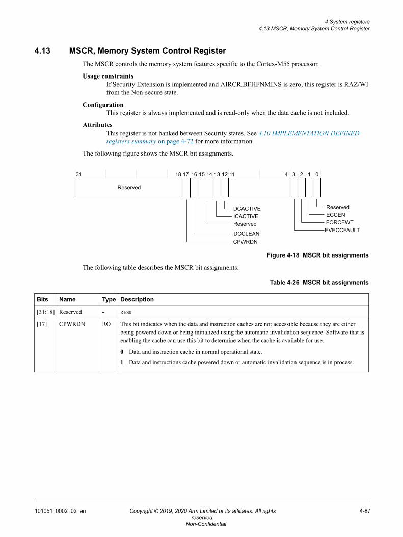
4.13 MSCR, Memory System Control RegisterThe MSCR controls the memory system features specific to the Cortex-M55 processor.
Usage constraintsIf Security Extension is implemented and AIRCR.BFHFNMINS is zero, this register is RAZ/WIfrom the Non-secure state.
ConfigurationThis register is always implemented and is read-only when the data cache is not included.
AttributesThis register is not banked between Security states. See 4.10 IMPLEMENTATION DEFINEDregisters summary on page 4-72 for more information.
The following figure shows the MSCR bit assignments.
31 16 15 4 3 014 13 12 11 2 117
ReservedECCENFORCEWTEVECCFAULT
DCACTIVEICACTIVE
DCCLEAN
Reserved
Reserved
CPWRDN
18
Figure 4-18 MSCR bit assignments
The following table describes the MSCR bit assignments.
Table 4-26 MSCR bit assignments
Bits Name Type Description
[31:18] Reserved - RES0
[17] CPWRDN RO This bit indicates when the data and instruction caches are not accessible because they are eitherbeing powered down or being initialized using the automatic invalidation sequence. Software that isenabling the cache can use this bit to determine when the cache is available for use.
0 Data and instruction cache in normal operational state.
1 Data and instructions cache powered down or automatic invalidation sequence is in process.
4 System registers4.13 MSCR, Memory System Control Register
101051_0002_02_en Copyright © 2019, 2020 Arm Limited or its affiliates. All rightsreserved.
4-87
Non-Confidential
Table 4-26 MSCR bit assignments (continued)
Bits Name Type Description
[16] DCCLEAN RW This bit indicates whether the data cache contains any dirty lines. The options are:
0 L1 data cache contains at least one dirty line.
1 L1 data cache does not contain any dirty lines.
It is cleared to 0 on any write to the L1 data cache that sets the dirty bit.
It is cleared to 1 at the end of any automatic L1 data cache invalidate all.
Software must only modify this register if it is restoring the state from before the core enteredpowerdown with the L1 data cache in retention.
This field is not updated when a dirty line is evicted, therefore, MCSR.DCCLEAN can be 0, if thecache is currently clean but previously contained dirty data since the last time it was automaticallyinvalidated.
The reset value is 0.
If the data cache is not included, this field is RAZ/WI.
[15:14] Reserved - RES0
[13] ICACTIVE RW This bit indicates whether the L1 instruction cache is active. The options are:
0 L1 instruction cache is inactive. There is no allocation or lookups. Cache maintenanceand direct cache access operations are treated as NOPs.
1 L1 instruction cache is active. This implies normal behavior.
The reset value is 1.
If the L1 instruction cache is not included, this field is RAZ/WI.
[12] DCACTIVE RW This bit indicates whether the L1 data cache is active. The options are:
0 L1 data cache is inactive. There is no allocation or lookups. Cache maintenance anddirect cache access operations are treated as NOPs.
1 L1 data cache is active. This implies normal behavior.
The reset value is 1.
If the L1 data cache is not included, this field is RAZ/WI.
[11:4] Reserved - RES0
[3] EVECCFAULT RW Enables asynchronous BusFault exceptions when data is lost on evictions. The options are:
0 Asynchronous BusFaults are not generated when evicting lines with multi-bit errors inthe data.
1 Asynchronous aborts are generated when evicting lines with multi-errors in the data.
This is intended for use in systems that do not support the AXI xPOISON signals. The reset value is1.
If ECC is not included, this field is RAZ/WI.
4 System registers4.13 MSCR, Memory System Control Register
101051_0002_02_en Copyright © 2019, 2020 Arm Limited or its affiliates. All rightsreserved.
4-88
Non-Confidential
Table 4-26 MSCR bit assignments (continued)
Bits Name Type Description
[2] FORCEWT RW Enables Forced Write-Through in the L1 data cache. The options are:
0 Force Write-Through is disabled.
1 Force Write-Through is enabled. All Cacheable memory regions are treated as Write-Through.
The reset value is 0.
If the L1 data cache is not included, this field is RAZ/WI.
[1] ECCEN RO Indicates whether Error Correcting Code (ECC) is present and enabled. The options are:
0 ECC not present or not enabled.
1 ECC present and enabled.
The reset value depends on the ECC Verilog parameter and the external input signal INITECCEN.For more information on ECC Verilog parameter, see the RTL configuration section in the Arm®
Cortex®-M55 Processor Integration and Implementation Manual.
If ECC is not included, this field is RAZ/WI.
[0] Reserved - RES0.
4 System registers4.13 MSCR, Memory System Control Register
101051_0002_02_en Copyright © 2019, 2020 Arm Limited or its affiliates. All rightsreserved.
4-89
Non-Confidential
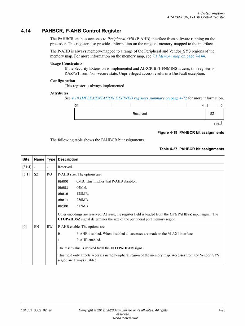
4.14 PAHBCR, P-AHB Control RegisterThe PAHBCR enables accesses to Peripheral AHB (P-AHB) interface from software running on theprocessor. This register also provides information on the range of memory-mapped to the interface.
The P-AHB is always memory-mapped to a range of the Peripheral and Vendor_SYS regions of thememory map. For more information on the memory map, see 7.1 Memory map on page 7-144.
Usage ConstraintsIf the Security Extension is implemented and AIRCR.BFHFNMINS is zero, this register isRAZ/WI from Non-secure state. Unprivileged access results in a BusFault exception.
ConfigurationThis register is always implemented.
AttributesSee 4.10 IMPLEMENTATION DEFINED registers summary on page 4-72 for more information.
Reserved
31 3 1 0
SZ
EN
4
Figure 4-19 PAHBCR bit assignments
The following table shows the PAHBCR bit assignments.
Table 4-27 PAHBCR bit assignments
Bits Name Type Description
[31:4] - - Reserved.
[3:1] SZ RO P-AHB size. The options are:
0b000 0MB. This implies that P-AHB disabled.
0b001 64MB.
0b010 128MB.
0b011 256MB.
0b100 512MB.
Other encodings are reserved. At reset, the register field is loaded from the CFGPAHBSZ input signal. TheCFGPAHBSZ signal determines the size of the peripheral port memory region.
[0] EN RW P-AHB enable. The options are:
0 P-AHB disabled. When disabled all accesses are made to the M-AXI interface.
1 P-AHB enabled.
The reset value is derived from the INITPAHBEN signal.
This field only affects accesses in the Peripheral region of the memory map. Accesses from the Vendor_SYSregion are always enabled.
4 System registers4.14 PAHBCR, P-AHB Control Register
101051_0002_02_en Copyright © 2019, 2020 Arm Limited or its affiliates. All rightsreserved.
4-90
Non-Confidential
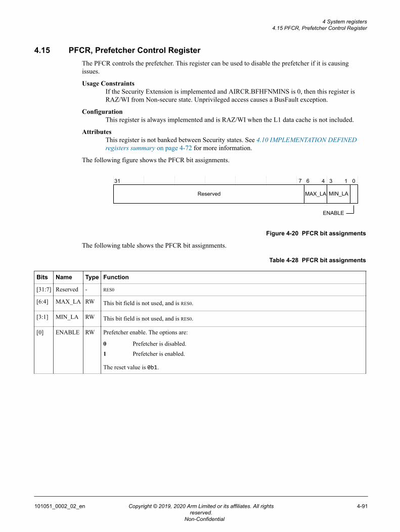
4.15 PFCR, Prefetcher Control RegisterThe PFCR controls the prefetcher. This register can be used to disable the prefetcher if it is causingissues.
Usage ConstraintsIf the Security Extension is implemented and AIRCR.BFHFNMINS is 0, then this register isRAZ/WI from Non-secure state. Unprivileged access causes a BusFault exception.
ConfigurationThis register is always implemented and is RAZ/WI when the L1 data cache is not included.
AttributesThis register is not banked between Security states. See 4.10 IMPLEMENTATION DEFINEDregisters summary on page 4-72 for more information.
The following figure shows the PFCR bit assignments.
31 4 3 07 6 1
ENABLE
Reserved MAX_LA MIN_LA
Figure 4-20 PFCR bit assignments
The following table shows the PFCR bit assignments.
Table 4-28 PFCR bit assignments
Bits Name Type Function
[31:7] Reserved - RES0
[6:4] MAX_LA RW This bit field is not used, and is RES0.
[3:1] MIN_LA RW This bit field is not used, and is RES0.
[0] ENABLE RW Prefetcher enable. The options are:
0 Prefetcher is disabled.
1 Prefetcher is enabled.
The reset value is 0b1.
4 System registers4.15 PFCR, Prefetcher Control Register
101051_0002_02_en Copyright © 2019, 2020 Arm Limited or its affiliates. All rightsreserved.
4-91
Non-Confidential
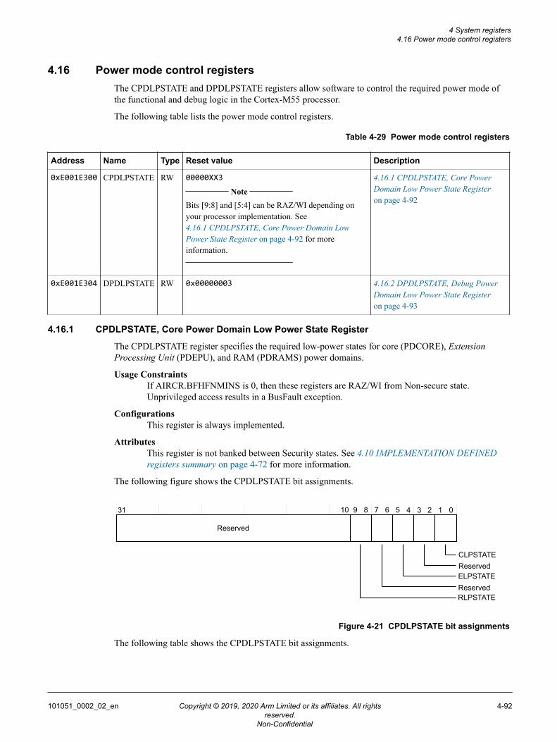
4.16 Power mode control registersThe CPDLPSTATE and DPDLPSTATE registers allow software to control the required power mode ofthe functional and debug logic in the Cortex-M55 processor.
The following table lists the power mode control registers.
Table 4-29 Power mode control registers
Address Name Type Reset value Description
0xE001E300 CPDLPSTATE RW 00000XX3 Note
Bits [9:8] and [5:4] can be RAZ/WI depending onyour processor implementation. See4.16.1 CPDLPSTATE, Core Power Domain LowPower State Register on page 4-92 for moreinformation.
4.16.1 CPDLPSTATE, Core PowerDomain Low Power State Registeron page 4-92
0xE001E304 DPDLPSTATE RW 0x00000003 4.16.2 DPDLPSTATE, Debug PowerDomain Low Power State Registeron page 4-93
4.16.1 CPDLPSTATE, Core Power Domain Low Power State Register
The CPDLPSTATE register specifies the required low-power states for core (PDCORE), ExtensionProcessing Unit (PDEPU), and RAM (PDRAMS) power domains.
Usage ConstraintsIf AIRCR.BFHFNMINS is 0, then these registers are RAZ/WI from Non-secure state.Unprivileged access results in a BusFault exception.
ConfigurationsThis register is always implemented.
AttributesThis register is not banked between Security states. See 4.10 IMPLEMENTATION DEFINEDregisters summary on page 4-72 for more information.
The following figure shows the CPDLPSTATE bit assignments.
31 4 3 010 9 8 7 6 5 2 1
Reserved
CLPSTATEReserved
ReservedELPSTATE
RLPSTATE
Figure 4-21 CPDLPSTATE bit assignments
The following table shows the CPDLPSTATE bit assignments.
4 System registers4.16 Power mode control registers
101051_0002_02_en Copyright © 2019, 2020 Arm Limited or its affiliates. All rightsreserved.
4-92
Non-Confidential
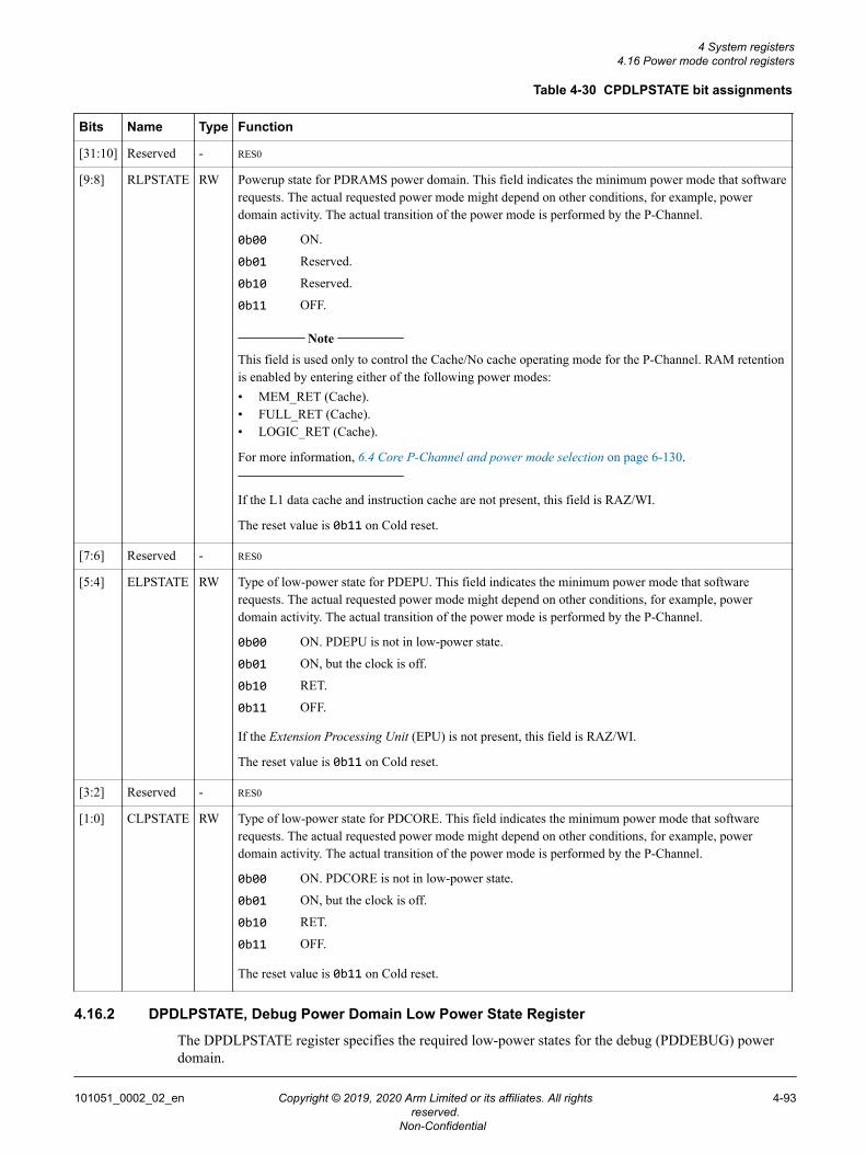
Table 4-30 CPDLPSTATE bit assignments
Bits Name Type Function
[31:10] Reserved - RES0
[9:8] RLPSTATE RW Powerup state for PDRAMS power domain. This field indicates the minimum power mode that softwarerequests. The actual requested power mode might depend on other conditions, for example, powerdomain activity. The actual transition of the power mode is performed by the P-Channel.
0b00 ON.
0b01 Reserved.
0b10 Reserved.
0b11 OFF.
Note
This field is used only to control the Cache/No cache operating mode for the P-Channel. RAM retentionis enabled by entering either of the following power modes:• MEM_RET (Cache).• FULL_RET (Cache).• LOGIC_RET (Cache).
For more information, 6.4 Core P-Channel and power mode selection on page 6-130.
If the L1 data cache and instruction cache are not present, this field is RAZ/WI.
The reset value is 0b11 on Cold reset.
[7:6] Reserved - RES0
[5:4] ELPSTATE RW Type of low-power state for PDEPU. This field indicates the minimum power mode that softwarerequests. The actual requested power mode might depend on other conditions, for example, powerdomain activity. The actual transition of the power mode is performed by the P-Channel.
0b00 ON. PDEPU is not in low-power state.
0b01 ON, but the clock is off.
0b10 RET.
0b11 OFF.
If the Extension Processing Unit (EPU) is not present, this field is RAZ/WI.
The reset value is 0b11 on Cold reset.
[3:2] Reserved - RES0
[1:0] CLPSTATE RW Type of low-power state for PDCORE. This field indicates the minimum power mode that softwarerequests. The actual requested power mode might depend on other conditions, for example, powerdomain activity. The actual transition of the power mode is performed by the P-Channel.
0b00 ON. PDCORE is not in low-power state.
0b01 ON, but the clock is off.
0b10 RET.
0b11 OFF.
The reset value is 0b11 on Cold reset.
4.16.2 DPDLPSTATE, Debug Power Domain Low Power State Register
The DPDLPSTATE register specifies the required low-power states for the debug (PDDEBUG) powerdomain.
4 System registers4.16 Power mode control registers
101051_0002_02_en Copyright © 2019, 2020 Arm Limited or its affiliates. All rightsreserved.
4-93
Non-Confidential
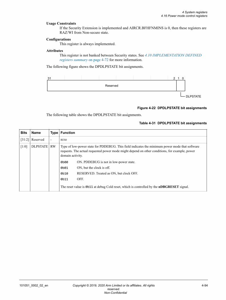
Usage ConstraintsIf the Security Extension is implemented and AIRCR.BFHFNMINS is 0, then these registers areRAZ/WI from Non-secure state.
ConfigurationsThis register is always implemented.
AttributesThis register is not banked between Security states. See 4.10 IMPLEMENTATION DEFINEDregisters summary on page 4-72 for more information.
The following figure shows the DPDLPSTATE bit assignments.
31 02 1
Reserved
DLPSTATE
Figure 4-22 DPDLPSTATE bit assignments
The following table shows the DPDLPSTATE bit assignments.
Table 4-31 DPDLPSTATE bit assignments
Bits Name Type Function
[31:2] Reserved - RES0
[1:0] DLPSTATE RW Type of low-power state for PDDEBUG. This field indicates the minimum power mode that softwarerequests. The actual requested power mode might depend on other conditions, for example, powerdomain activity.
0b00 ON. PDDEBUG is not in low-power state.
0b01 ON, but the clock is off.
0b10 RESERVED. Treated as ON, but clock OFF.
0b11 OFF.
The reset value is 0b11 at debug Cold reset, which is controlled by the nDBGRESET signal.
4 System registers4.16 Power mode control registers
101051_0002_02_en Copyright © 2019, 2020 Arm Limited or its affiliates. All rightsreserved.
4-94
Non-Confidential
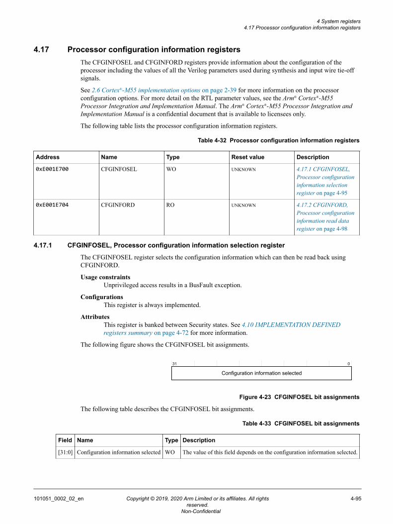
4.17 Processor configuration information registersThe CFGINFOSEL and CFGINFORD registers provide information about the configuration of theprocessor including the values of all the Verilog parameters used during synthesis and input wire tie-offsignals.
See 2.6 Cortex®-M55 implementation options on page 2-39 for more information on the processorconfiguration options. For more detail on the RTL parameter values, see the Arm® Cortex®-M55Processor Integration and Implementation Manual. The Arm® Cortex®-M55 Processor Integration andImplementation Manual is a confidential document that is available to licensees only.
The following table lists the processor configuration information registers.
Table 4-32 Processor configuration information registers
Address Name Type Reset value Description
0xE001E700 CFGINFOSEL WO UNKNOWN 4.17.1 CFGINFOSEL,Processor configurationinformation selectionregister on page 4-95
0xE001E704 CFGINFORD RO UNKNOWN 4.17.2 CFGINFORD,Processor configurationinformation read dataregister on page 4-98
4.17.1 CFGINFOSEL, Processor configuration information selection register
The CFGINFOSEL register selects the configuration information which can then be read back usingCFGINFORD.
Usage constraintsUnprivileged access results in a BusFault exception.
ConfigurationsThis register is always implemented.
AttributesThis register is banked between Security states. See 4.10 IMPLEMENTATION DEFINEDregisters summary on page 4-72 for more information.
The following figure shows the CFGINFOSEL bit assignments.
31 0
Configuration information selected
Figure 4-23 CFGINFOSEL bit assignments
The following table describes the CFGINFOSEL bit assignments.
Table 4-33 CFGINFOSEL bit assignments
Field Name Type Description
[31:0] Configuration information selected WO The value of this field depends on the configuration information selected.
4 System registers4.17 Processor configuration information registers
101051_0002_02_en Copyright © 2019, 2020 Arm Limited or its affiliates. All rightsreserved.
4-95
Non-Confidential
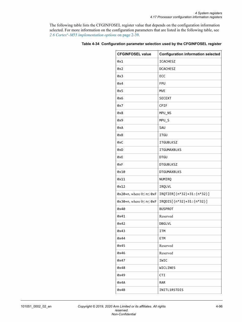
The following table lists the CFGINFOSEL register value that depends on the configuration informationselected. For more information on the configuration parameters that are listed in the following table, see2.6 Cortex®-M55 implementation options on page 2-39.
Table 4-34 Configuration parameter selection used by the CFGINFOSEL register
CFGINFOSEL value Configuration information selected
0x1 ICACHESZ
0x2 DCACHESZ
0x3 ECC
0x4 FPU
0x5 MVE
0x6 SECEXT
0x7 CPIF
0x8 MPU_NS
0x9 MPU_S
0xA SAU
0xB ITGU
0xC ITGUBLKSZ
0xD ITGUMAXBLKS
0xE DTGU
0xF DTGUBLKSZ
0x10 DTGUMAXBLKS
0x11 NUMIRQ
0x12 IRQLVL
0x20+n, where 0≤ n≤ 0xF IRQTIER[(n*32)+31:(n*32)]
0x30+n, where 0≤ n≤ 0xF IRQDIS[(n*32)+31:(n*32)]
0x40 BUSPROT
0x41 Reserved
0x42 DBGLVL
0x43 ITM
0x44 ETM
0x45 Reserved
0x46 Reserved
0x47 IWIC
0x48 WICLINES
0x49 CTI
0x4A RAR
0x4B INITL1RSTDIS
4 System registers4.17 Processor configuration information registers
101051_0002_02_en Copyright © 2019, 2020 Arm Limited or its affiliates. All rightsreserved.
4-96
Non-Confidential
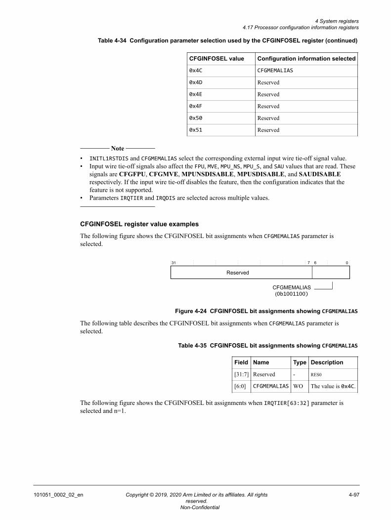
Table 4-34 Configuration parameter selection used by the CFGINFOSEL register (continued)
CFGINFOSEL value Configuration information selected
0x4C CFGMEMALIAS
0x4D Reserved
0x4E Reserved
0x4F Reserved
0x50 Reserved
0x51 Reserved
Note
• INITL1RSTDIS and CFGMEMALIAS select the corresponding external input wire tie-off signal value.• Input wire tie-off signals also affect the FPU, MVE, MPU_NS, MPU_S, and SAU values that are read. These
signals are CFGFPU, CFGMVE, MPUNSDISABLE, MPUSDISABLE, and SAUDISABLErespectively. If the input wire tie-off disables the feature, then the configuration indicates that thefeature is not supported.
• Parameters IRQTIER and IRQDIS are selected across multiple values.
CFGINFOSEL register value examples
The following figure shows the CFGINFOSEL bit assignments when CFGMEMALIAS parameter isselected.
31 0
CFGMEMALIAS (0b1001100)
67
Reserved
Figure 4-24 CFGINFOSEL bit assignments showing CFGMEMALIAS
The following table describes the CFGINFOSEL bit assignments when CFGMEMALIAS parameter isselected.
Table 4-35 CFGINFOSEL bit assignments showing CFGMEMALIAS
Field Name Type Description
[31:7] Reserved - RES0
[6:0] CFGMEMALIAS WO The value is 0x4C.
The following figure shows the CFGINFOSEL bit assignments when IRQTIER[63:32] parameter isselected and n=1.
4 System registers4.17 Processor configuration information registers
101051_0002_02_en Copyright © 2019, 2020 Arm Limited or its affiliates. All rightsreserved.
4-97
Non-Confidential
31 6 5 0
ReservedIRQTIER
(0b100001)
Figure 4-25 CFGINFOSEL bit assignments showing IRQTIER when n=1
The following table describes the CFGINFOSEL bit assignments showing IRQTIER[63:32] when n=1.
Table 4-36 CFGINFOSEL bit assignments showing IRQTIER when n=1
Field Name Type Description
[31:6] Reserved - RES0
[5:0] IRQTIER WO The value is 0x21, indicating IRQTIER[63:32] .
4.17.2 CFGINFORD, Processor configuration information read data register
The CFGINFORD register can be used to display the configuration information that the CFGINFOSELregister selects.
Usage constraintsUnprivileged access results in a BusFault exception.
ConfigurationsThis register is always implemented.
AttributesThis register is banked between Security states. See 4.10 IMPLEMENTATION DEFINEDregisters summary on page 4-72 for more information.
The following figure shows the CFGINFORD bit assignments.
31 0
Configuration information displayed
Figure 4-26 CFGINFORD bit assignments
The following table describes the CFGINFORD bit assignments.
Table 4-37 CFGINFORD bit assignments
Field Name Type Description
[31:0] Configuration information displayed RO The value of this field depends on the configuration information selected.
CFGINFORD register value examples
The following figure shows the CFGINFORD bit assignments when the CFGINFOSEL register selectsthe CFGMEMALIAS parameter.
4 System registers4.17 Processor configuration information registers
101051_0002_02_en Copyright © 2019, 2020 Arm Limited or its affiliates. All rightsreserved.
4-98
Non-Confidential
31 0
CFGMEMALIAS(0b10000)
45
RES0
Figure 4-27 CFGINFORD bit assignments showing CFGMEMALIAS
The following table describes the CFGINFORD bit assignments when CFGMEMALIAS configurationinput signal is selected and the alias bit selected is 28.
Table 4-38 CFGINFORD bit assignments showing CFGMEMALIAS
Field Name Type Description
[31:5] Reserved - RES0
[4:0] CFGMEMALIAS RO The value that is displayed is 0b10000 to indicate that alias bit 28 has been selected.
The following figure shows the CFGINFORD bit assignments when IRQTIER parameter is selected andn=1.
63 32
IRQTIER
Figure 4-28 CFGINFORD bit assignments showing IRQTIER when n=1
The following table describes the CFGINFOSEL bit assignments showing IRQTIER[63:32] when n=1.For this example, we are assuming that IRQTIER[63:32] is 0 for all interrupts, indicating lowest latencyfor IRQ32 to IRQ63.
Table 4-39 CFGINFORD bit assignments showing IRQTIER when n=1
Field Name Type Description
[63:32] IRQTIER RO 0x00000000
4 System registers4.17 Processor configuration information registers
101051_0002_02_en Copyright © 2019, 2020 Arm Limited or its affiliates. All rightsreserved.
4-99
Non-Confidential
4.18 ID_PFR0, Processor Feature Register 0The ID_PFR0 register contains a field that indicates the version of the Reliability, Availability, andServiceability (RAS) extension supported.
Usage constraintsUnprivileged access results in a BusFault exception.This register is accessible through unprivileged Debug AHB (D-AHB) debug requests wheneither DAUTHCTRL_S.UIDAPEN or DAUTHCTRL_NS.UIDAPEN is set.
ConfigurationsThis register is always implemented.
AttributesThis register is not banked between Security states. See 4.10 IMPLEMENTATION DEFINEDregisters summary on page 4-72 for more information.
The following figure shows the ID_PFR0 bit assignments.
31 0
RAS
8 7
Reserved State0
28 27 4 3
State1
Figure 4-29 ID_PFR0 bit assignments
The following table describes the ID_PFR0 bit assignments.
Table 4-40 ID_PFR0 bit assignments
Field Name Type Description
[31:28] RAS RO Identifies which version of the RAS architecture is implemented.
0b0010 Version 1.
[27:8] Reserved - RES0
[7:4] State1 RO T32 instruction set support.
0b0011 T32 instruction set including Thumb-2 technology is implemented.
[3:0] State0 RO A32 instruction set support.
0b0000 A32 instruction set is not implemented.
4 System registers4.18 ID_PFR0, Processor Feature Register 0
101051_0002_02_en Copyright © 2019, 2020 Arm Limited or its affiliates. All rightsreserved.
4-100
Non-Confidential
4.19 ITCMCR and DTCMCR, TCM Control RegistersThe ITCMCR and DTCMCR registers enable access to the Tightly Coupled Memories (TCMs) bysoftware running on the processor. These registers also provide information on the physical size of thememory connected.
Usage ConstraintsIf the Security Extension is implemented and AIRCR.BFHFNMINS is 0, then these registers areRAZ/WI from Non-secure state. Unprivileged access results in a BusFault exception.If the external input signal, LOCKTCM is asserted, these registers are read-only. For moreinformation on LOCKTCM, see C.27 Miscellaneous signals on page Appx-C-413.
ConfigurationThese registers are always implemented.
AttributesThese registers are not banked between Security states. See 4.10 IMPLEMENTATIONDEFINED registers summary on page 4-72 for more information.
The following figure shows the ITCMCR and DTCMCR bit assignments.
31 7 6 3 2 1 0
Reserved SZ
Reseved
EN
Figure 4-30 ITCMCR and DTCMCR bit assignments
The following table shows the ITCMCR and DTCMCR bit assignments.
4 System registers4.19 ITCMCR and DTCMCR, TCM Control Registers
101051_0002_02_en Copyright © 2019, 2020 Arm Limited or its affiliates. All rightsreserved.
4-101
Non-Confidential
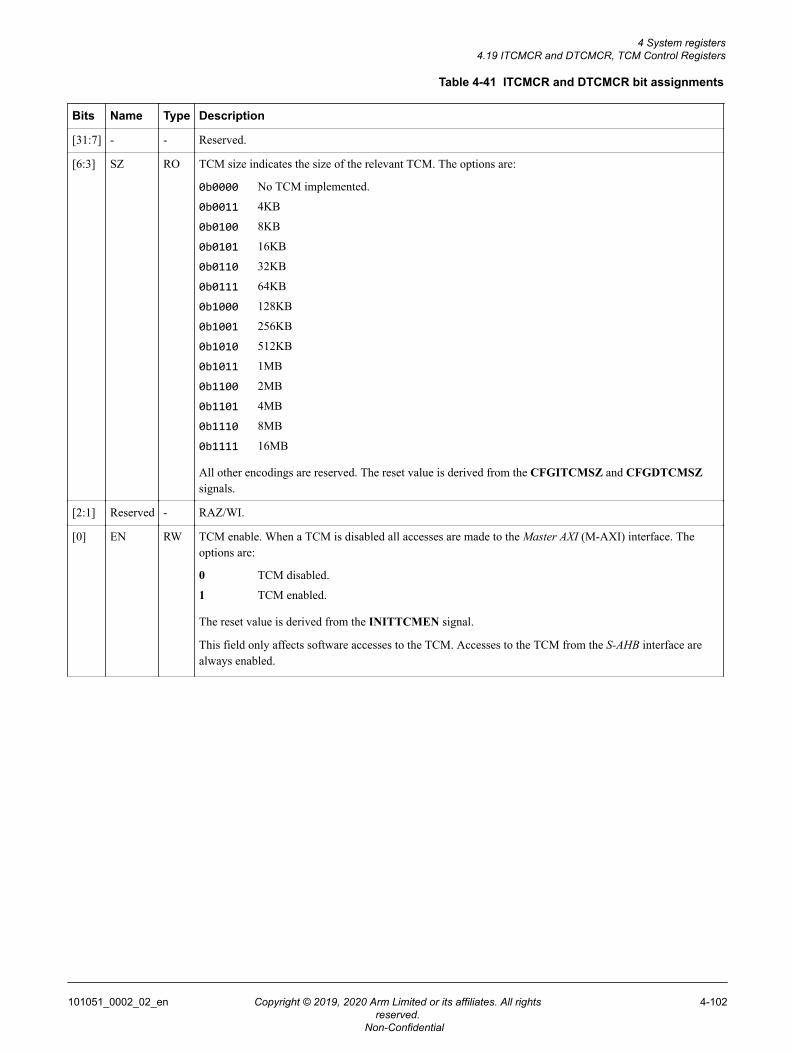
Table 4-41 ITCMCR and DTCMCR bit assignments
Bits Name Type Description
[31:7] - - Reserved.
[6:3] SZ RO TCM size indicates the size of the relevant TCM. The options are:
0b0000 No TCM implemented.
0b0011 4KB
0b0100 8KB
0b0101 16KB
0b0110 32KB
0b0111 64KB
0b1000 128KB
0b1001 256KB
0b1010 512KB
0b1011 1MB
0b1100 2MB
0b1101 4MB
0b1110 8MB
0b1111 16MB
All other encodings are reserved. The reset value is derived from the CFGITCMSZ and CFGDTCMSZsignals.
[2:1] Reserved - RAZ/WI.
[0] EN RW TCM enable. When a TCM is disabled all accesses are made to the Master AXI (M-AXI) interface. Theoptions are:
0 TCM disabled.
1 TCM enabled.
The reset value is derived from the INITTCMEN signal.
This field only affects software accesses to the TCM. Accesses to the TCM from the S-AHB interface arealways enabled.
4 System registers4.19 ITCMCR and DTCMCR, TCM Control Registers
101051_0002_02_en Copyright © 2019, 2020 Arm Limited or its affiliates. All rightsreserved.
4-102
Non-Confidential
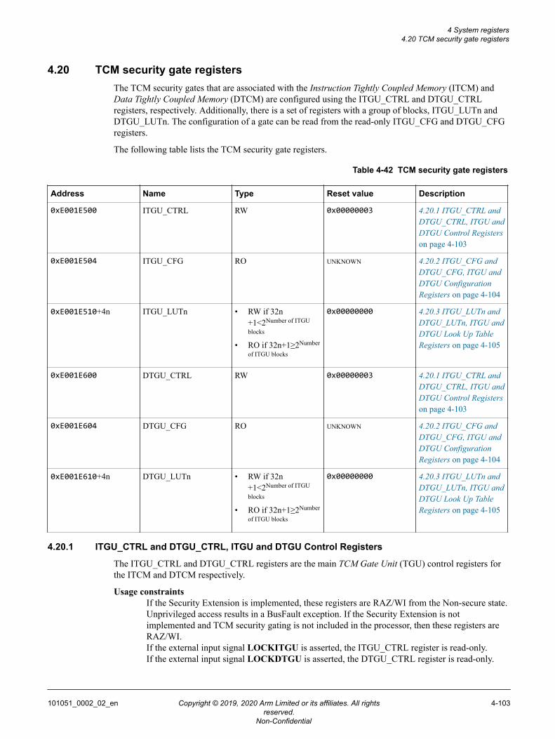
4.20 TCM security gate registersThe TCM security gates that are associated with the Instruction Tightly Coupled Memory (ITCM) andData Tightly Coupled Memory (DTCM) are configured using the ITGU_CTRL and DTGU_CTRLregisters, respectively. Additionally, there is a set of registers with a group of blocks, ITGU_LUTn andDTGU_LUTn. The configuration of a gate can be read from the read-only ITGU_CFG and DTGU_CFGregisters.
The following table lists the TCM security gate registers.
Table 4-42 TCM security gate registers
Address Name Type Reset value Description
0xE001E500 ITGU_CTRL RW 0x00000003 4.20.1 ITGU_CTRL andDTGU_CTRL, ITGU andDTGU Control Registerson page 4-103
0xE001E504 ITGU_CFG RO UNKNOWN 4.20.2 ITGU_CFG andDTGU_CFG, ITGU andDTGU ConfigurationRegisters on page 4-104
0xE001E510+4n ITGU_LUTn • RW if 32n+1<2Number of ITGU
blocks
• RO if 32n+1≥2Number
of ITGU blocks
0x00000000 4.20.3 ITGU_LUTn andDTGU_LUTn, ITGU andDTGU Look Up TableRegisters on page 4-105
0xE001E600 DTGU_CTRL RW 0x00000003 4.20.1 ITGU_CTRL andDTGU_CTRL, ITGU andDTGU Control Registerson page 4-103
0xE001E604 DTGU_CFG RO UNKNOWN 4.20.2 ITGU_CFG andDTGU_CFG, ITGU andDTGU ConfigurationRegisters on page 4-104
0xE001E610+4n DTGU_LUTn • RW if 32n+1<2Number of ITGU
blocks
• RO if 32n+1≥2Number
of ITGU blocks
0x00000000 4.20.3 ITGU_LUTn andDTGU_LUTn, ITGU andDTGU Look Up TableRegisters on page 4-105
4.20.1 ITGU_CTRL and DTGU_CTRL, ITGU and DTGU Control Registers
The ITGU_CTRL and DTGU_CTRL registers are the main TCM Gate Unit (TGU) control registers forthe ITCM and DTCM respectively.
Usage constraintsIf the Security Extension is implemented, these registers are RAZ/WI from the Non-secure state.Unprivileged access results in a BusFault exception. If the Security Extension is notimplemented and TCM security gating is not included in the processor, then these registers areRAZ/WI.If the external input signal LOCKITGU is asserted, the ITGU_CTRL register is read-only.If the external input signal LOCKDTGU is asserted, the DTGU_CTRL register is read-only.
4 System registers4.20 TCM security gate registers
101051_0002_02_en Copyright © 2019, 2020 Arm Limited or its affiliates. All rightsreserved.
4-103
Non-Confidential
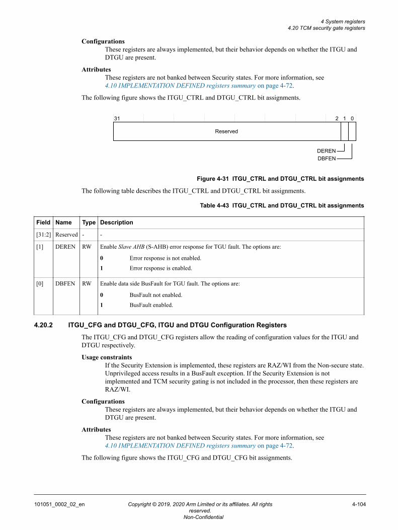
ConfigurationsThese registers are always implemented, but their behavior depends on whether the ITGU andDTGU are present.
AttributesThese registers are not banked between Security states. For more information, see4.10 IMPLEMENTATION DEFINED registers summary on page 4-72.
The following figure shows the ITGU_CTRL and DTGU_CTRL bit assignments.
31 02 1
DERENDBFEN
Reserved
Figure 4-31 ITGU_CTRL and DTGU_CTRL bit assignments
The following table describes the ITGU_CTRL and DTGU_CTRL bit assignments.
Table 4-43 ITGU_CTRL and DTGU_CTRL bit assignments
Field Name Type Description
[31:2] Reserved - -
[1] DEREN RW Enable Slave AHB (S-AHB) error response for TGU fault. The options are:
0 Error response is not enabled.
1 Error response is enabled.
[0] DBFEN RW Enable data side BusFault for TGU fault. The options are:
0 BusFault not enabled.
1 BusFault enabled.
4.20.2 ITGU_CFG and DTGU_CFG, ITGU and DTGU Configuration Registers
The ITGU_CFG and DTGU_CFG registers allow the reading of configuration values for the ITGU andDTGU respectively.
Usage constraintsIf the Security Extension is implemented, these registers are RAZ/WI from the Non-secure state.Unprivileged access results in a BusFault exception. If the Security Extension is notimplemented and TCM security gating is not included in the processor, then these registers areRAZ/WI.
ConfigurationsThese registers are always implemented, but their behavior depends on whether the ITGU andDTGU are present.
AttributesThese registers are not banked between Security states. For more information, see4.10 IMPLEMENTATION DEFINED registers summary on page 4-72.
The following figure shows the ITGU_CFG and DTGU_CFG bit assignments.
4 System registers4.20 TCM security gate registers
101051_0002_02_en Copyright © 2019, 2020 Arm Limited or its affiliates. All rightsreserved.
4-104
Non-Confidential
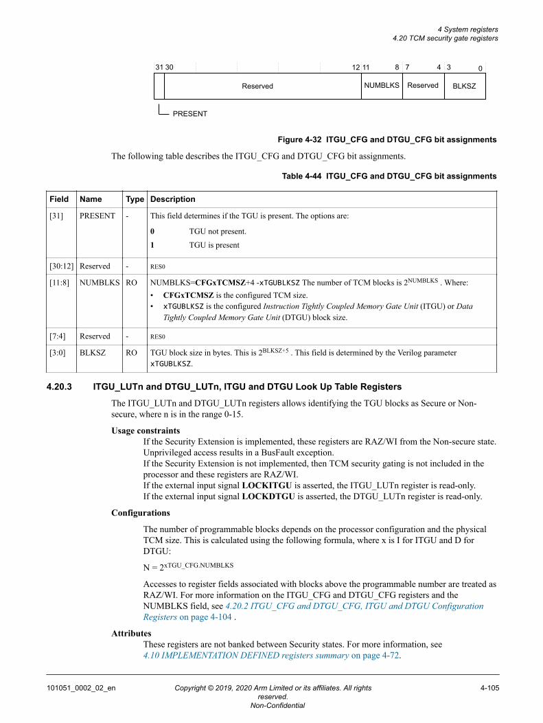
31 4 0
Reserved NUMBLKS BLKSZ
PRESENT
30 12 11 8 7 3
Reserved
Figure 4-32 ITGU_CFG and DTGU_CFG bit assignments
The following table describes the ITGU_CFG and DTGU_CFG bit assignments.
Table 4-44 ITGU_CFG and DTGU_CFG bit assignments
Field Name Type Description
[31] PRESENT - This field determines if the TGU is present. The options are:
0 TGU not present.
1 TGU is present
[30:12] Reserved - RES0
[11:8] NUMBLKS RO NUMBLKS=CFGxTCMSZ+4 -xTGUBLKSZ The number of TCM blocks is 2NUMBLKS . Where:• CFGxTCMSZ is the configured TCM size.• xTGUBLKSZ is the configured Instruction Tightly Coupled Memory Gate Unit (ITGU) or Data
Tightly Coupled Memory Gate Unit (DTGU) block size.
[7:4] Reserved - RES0
[3:0] BLKSZ RO TGU block size in bytes. This is 2BLKSZ+5 . This field is determined by the Verilog parameterxTGUBLKSZ.
4.20.3 ITGU_LUTn and DTGU_LUTn, ITGU and DTGU Look Up Table Registers
The ITGU_LUTn and DTGU_LUTn registers allows identifying the TGU blocks as Secure or Non-secure, where n is in the range 0-15.
Usage constraintsIf the Security Extension is implemented, these registers are RAZ/WI from the Non-secure state.Unprivileged access results in a BusFault exception.If the Security Extension is not implemented, then TCM security gating is not included in theprocessor and these registers are RAZ/WI.If the external input signal LOCKITGU is asserted, the ITGU_LUTn register is read-only.If the external input signal LOCKDTGU is asserted, the DTGU_LUTn register is read-only.
Configurations
The number of programmable blocks depends on the processor configuration and the physicalTCM size. This is calculated using the following formula, where x is I for ITGU and D forDTGU:
N = 2xTGU_CFG.NUMBLKS
Accesses to register fields associated with blocks above the programmable number are treated asRAZ/WI. For more information on the ITGU_CFG and DTGU_CFG registers and theNUMBLKS field, see 4.20.2 ITGU_CFG and DTGU_CFG, ITGU and DTGU ConfigurationRegisters on page 4-104 .
AttributesThese registers are not banked between Security states. For more information, see4.10 IMPLEMENTATION DEFINED registers summary on page 4-72.
4 System registers4.20 TCM security gate registers
101051_0002_02_en Copyright © 2019, 2020 Arm Limited or its affiliates. All rightsreserved.
4-105
Non-Confidential
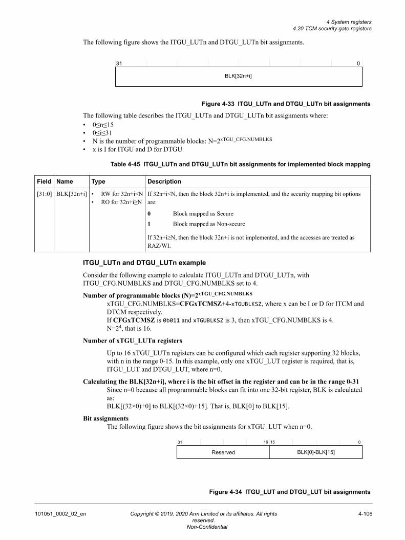
The following figure shows the ITGU_LUTn and DTGU_LUTn bit assignments.
31 0
BLK[32n+i]
Figure 4-33 ITGU_LUTn and DTGU_LUTn bit assignments
The following table describes the ITGU_LUTn and DTGU_LUTn bit assignments where:• 0≤n≤15• 0≤i≤31• N is the number of programmable blocks: N=2xTGU_CFG.NUMBLKS
• x is I for ITGU and D for DTGU
Table 4-45 ITGU_LUTn and DTGU_LUTn bit assignments for implemented block mapping
Field Name Type Description
[31:0] BLK[32n+i] • RW for 32n+i<N• RO for 32n+i≥N
If 32n+i<N, then the block 32n+i is implemented, and the security mapping bit optionsare:
0 Block mapped as Secure
1 Block mapped as Non-secure
If 32n+i≥N, then the block 32n+i is not implemented, and the accesses are treated asRAZ/WI.
ITGU_LUTn and DTGU_LUTn example
Consider the following example to calculate ITGU_LUTn and DTGU_LUTn, withITGU_CFG.NUMBLKS and DTGU_CFG.NUMBLKS set to 4.
Number of programmable blocks (N)=2xTGU_CFG.NUMBLKS
xTGU_CFG.NUMBLKS=CFGxTCMSZ+4-xTGUBLKSZ, where x can be I or D for ITCM andDTCM respectively.If CFGxTCMSZ is 0b011 and xTGUBLKSZ is 3, then xTGU_CFG.NUMBLKS is 4.N=24, that is 16.
Number of xTGU_LUTn registers
Up to 16 xTGU_LUTn registers can be configured which each register supporting 32 blocks,with n in the range 0-15. In this example, only one xTGU_LUT register is required, that is,ITGU_LUT and DTGU_LUT, where n=0.
Calculating the BLK[32n+i], where i is the bit offset in the register and can be in the range 0-31Since n=0 because all programmable blocks can fit into one 32-bit register, BLK is calculatedas:BLK[(32×0)+0] to BLK[(32×0)+15]. That is, BLK[0] to BLK[15].
Bit assignmentsThe following figure shows the bit assignments for xTGU_LUT when n=0.
31 0
BLK[0]-BLK[15]
1516
Reserved
Figure 4-34 ITGU_LUT and DTGU_LUT bit assignments
4 System registers4.20 TCM security gate registers
101051_0002_02_en Copyright © 2019, 2020 Arm Limited or its affiliates. All rightsreserved.
4-106
Non-Confidential
The following table describes the bit assignments.
Table 4-46 ITGU_LUTn and DTGU_LUTn bit assignments for implemented block mapping
Field Name Type Description
[31:16] - RO RAZ/WI.
[15:0] BLK[0] to BLK[15] RW If 32n+i<N, then the implemented block 32n+i security mapping bit options are:
0 Block mapped as Secure.1 Block mapped as Non-secure.
4 System registers4.20 TCM security gate registers
101051_0002_02_en Copyright © 2019, 2020 Arm Limited or its affiliates. All rightsreserved.
4-107
Non-Confidential
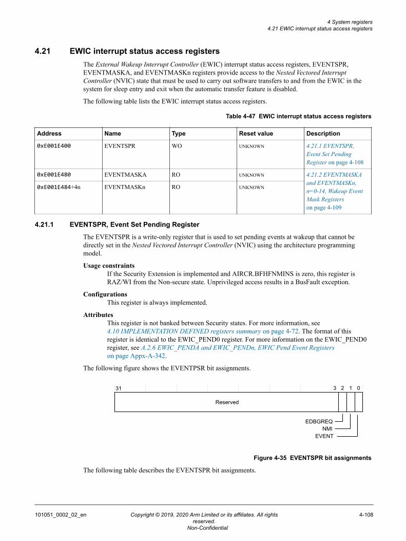
4.21 EWIC interrupt status access registersThe External Wakeup Interrupt Controller (EWIC) interrupt status access registers, EVENTSPR,EVENTMASKA, and EVENTMASKn registers provide access to the Nested Vectored InterruptController (NVIC) state that must be used to carry out software transfers to and from the EWIC in thesystem for sleep entry and exit when the automatic transfer feature is disabled.
The following table lists the EWIC interrupt status access registers.
Table 4-47 EWIC interrupt status access registers
Address Name Type Reset value Description
0xE001E400 EVENTSPR WO UNKNOWN 4.21.1 EVENTSPR,Event Set PendingRegister on page 4-108
0xE001E480 EVENTMASKA RO UNKNOWN 4.21.2 EVENTMASKAand EVENTMASKn,n=0-14, Wakeup EventMask Registerson page 4-109
0xE001E484+4n EVENTMASKn RO UNKNOWN
4.21.1 EVENTSPR, Event Set Pending Register
The EVENTSPR is a write-only register that is used to set pending events at wakeup that cannot bedirectly set in the Nested Vectored Interrupt Controller (NVIC) using the architecture programmingmodel.
Usage constraintsIf the Security Extension is implemented and AIRCR.BFHFNMINS is zero, this register isRAZ/WI from the Non-secure state. Unprivileged access results in a BusFault exception.
ConfigurationsThis register is always implemented.
AttributesThis register is not banked between Security states. For more information, see4.10 IMPLEMENTATION DEFINED registers summary on page 4-72. The format of thisregister is identical to the EWIC_PEND0 register. For more information on the EWIC_PEND0register, see A.2.6 EWIC_PENDA and EWIC_PENDn, EWIC Pend Event Registerson page Appx-A-342.
The following figure shows the EVENTPSR bit assignments.
31 0
Reserved
1
EDBGREQ
23
NMIEVENT
Figure 4-35 EVENTSPR bit assignments
The following table describes the EVENTSPR bit assignments.
4 System registers4.21 EWIC interrupt status access registers
101051_0002_02_en Copyright © 2019, 2020 Arm Limited or its affiliates. All rightsreserved.
4-108
Non-Confidential
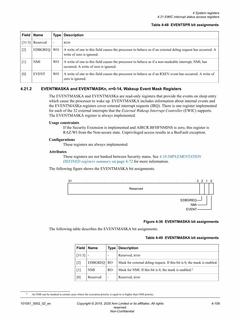
Table 4-48 EVENTSPR bit assignments
Field Name Type Description
[31:3] Reserved - RES0
[2] EDBGREQ WO A write of one to this field causes the processor to behave as if an external debug request has occurred. Awrite of zero is ignored.
[1] NMI WO A write of one to this field causes the processor to behave as if a non-maskable interrupt, NMI, hasoccurred. A write of zero is ignored.
[0] EVENT WO A write of one to this field causes the processor to behave as if an RXEV event has occurred. A write ofzero is ignored.
4.21.2 EVENTMASKA and EVENTMASKn, n=0-14, Wakeup Event Mask Registers
The EVENTMASKA and EVENTMASKn are read-only registers that provide the events on sleep entrywhich cause the processor to wake up. EVENTMASKA includes information about internal events andthe EVENTMASKn registers cover external interrupt requests (IRQ). There is one register implementedfor each of the 32 external interrupts that the External Wakeup Interrupt Controller (EWIC) supports.The EVENTMASKA register is always implemented.
Usage constraintsIf the Security Extension is implemented and AIRCR.BFHFNMINS is zero, this register isRAZ/WI from the Non-secure state. Unprivileged access results in a BusFault exception.
ConfigurationsThese registers are always implemented.
AttributesThese registers are not banked between Security states. See 4.10 IMPLEMENTATIONDEFINED registers summary on page 4-72 for more information.
The following figure shows the EVENTMASKA bit assignments.
31 01
EDBGREQ
Reserved
23
NMIEVENT
Figure 4-36 EVENTMASKA bit assignments
The following table describes the EVENTMASKA bit assignments.
Table 4-49 EVENTMASKA bit assignments
Field Name Type Description
[31:3] - - Reserved, RES0
[2] EDBGREQ RO Mask for external debug request. If this bit is 0, the mask is enabled.
[1] NMI RO Mask for NMI. If this bit is 0, the mask is enabled.a
[0] Reserved - Reserved, RES0
a An NMI can be masked in certain cases where the execution priority is equal to or higher than NMI priority.
4 System registers4.21 EWIC interrupt status access registers
101051_0002_02_en Copyright © 2019, 2020 Arm Limited or its affiliates. All rightsreserved.
4-109
Non-Confidential
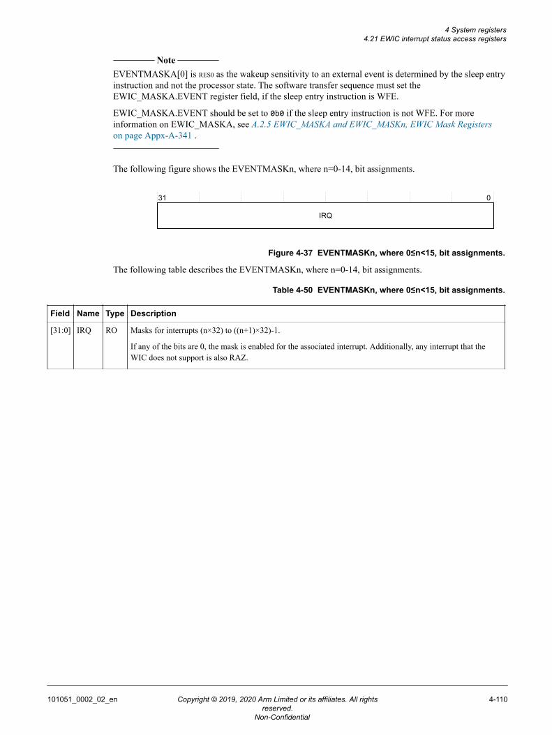
Note
EVENTMASKA[0] is RES0 as the wakeup sensitivity to an external event is determined by the sleep entryinstruction and not the processor state. The software transfer sequence must set theEWIC_MASKA.EVENT register field, if the sleep entry instruction is WFE.
EWIC_MASKA.EVENT should be set to 0b0 if the sleep entry instruction is not WFE. For moreinformation on EWIC_MASKA, see A.2.5 EWIC_MASKA and EWIC_MASKn, EWIC Mask Registerson page Appx-A-341 .
The following figure shows the EVENTMASKn, where n=0-14, bit assignments.
31 0
IRQ
Figure 4-37 EVENTMASKn, where 0≤n<15, bit assignments.
The following table describes the EVENTMASKn, where n=0-14, bit assignments.
Table 4-50 EVENTMASKn, where 0≤n<15, bit assignments.
Field Name Type Description
[31:0] IRQ RO Masks for interrupts (n×32) to ((n+1)×32)-1.
If any of the bits are 0, the mask is enabled for the associated interrupt. Additionally, any interrupt that theWIC does not support is also RAZ.
4 System registers4.21 EWIC interrupt status access registers
101051_0002_02_en Copyright © 2019, 2020 Arm Limited or its affiliates. All rightsreserved.
4-110
Non-Confidential
Chapter 5Initialization
This chapter describes how to initialize the Cortex-M55 processor and which registers to access to enablefunctionality before using the processor features.
It contains the following sections:• 5.1 Initialization overview on page 5-112.• 5.2 Initializing and reprogramming the MPU on page 5-113.• 5.3 Initializing the EPU on page 5-114.• 5.4 Programming the SAU on page 5-115.• 5.5 Initializing the instruction and data cache on page 5-116.• 5.6 Enabling the branch cache on page 5-118.• 5.7 Enabling and preloading the TCM on page 5-119.• 5.8 Enabling and locking the TCM security gates on page 5-120.• 5.9 Enabling the P-AHB interface on page 5-121.
101051_0002_02_en Copyright © 2019, 2020 Arm Limited or its affiliates. All rightsreserved.
5-111
Non-Confidential
5.1 Initialization overviewBefore your run your application, you might want to program values into registers and memory andenable certain processor features.
This chapter describes other initialization requirements, some of which are optional depending on thefeatures you have implemented in the Cortex-M55 processor.
5 Initialization5.1 Initialization overview
101051_0002_02_en Copyright © 2019, 2020 Arm Limited or its affiliates. All rightsreserved.
5-112
Non-Confidential
5.2 Initializing and reprogramming the MPUThe Cortex-M55 processor can be configured to include the Memory Protection Unit (MPU), which is anoptional component that is primarily used for memory region protection.
If the Security Extension is included in the Cortex-M55 processor, memory protection logic can be splitbetween Secure and Non-secure MPU (MPU_S and MPU_NS).
Memory protection logic can be split between Secure and Non-secure MPU (MPU_S and MPU_NS).
The MPU_CTRL.ENABLE must be set to 1 to enable the MPU.
If the Security Extension is included, then MPU_CTRL_NS is the Non-secure version of this register,and can be used to enable the Non-secure MPU region. For more information on MPU_CTRL, see theArm®v8-M Architecture Reference Manual.
Note
For more information on the MPU, see 8.3 Memory Protection Unit on page 8-159.
Reprogramming the MPUWhen setting up the MPU, and if it has been previously programmed, disable unused regions to preventany old settings from affecting the latest MPU setup.1. Execute a DSB instruction, to drain out any existing memory transactions.2. Write to the MPU registers. For a complete list, see 8.3.1 Memory Protection Unit register summary
on page 8-159.3. Execute a DSB instruction and then an ISB instruction, to ensure that all subsequent memory accesses
see the updated MPU setup. Remember
Additionally, if any memory is converted from Cacheable to Non-cacheable or Device, and any write hasbeen performed to that memory, you must perform data cache clean and invalidate operations (DCIMVAC)each of these cachelines.
For more information on these operations, see the Arm®v8-M Architecture Reference Manual.
5 Initialization5.2 Initializing and reprogramming the MPU
101051_0002_02_en Copyright © 2019, 2020 Arm Limited or its affiliates. All rightsreserved.
5-113
Non-Confidential
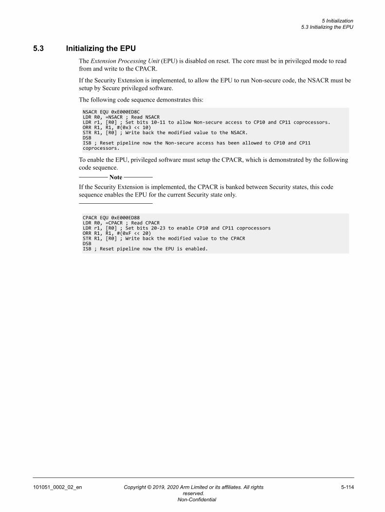
5.3 Initializing the EPUThe Extension Processing Unit (EPU) is disabled on reset. The core must be in privileged mode to readfrom and write to the CPACR.
If the Security Extension is implemented, to allow the EPU to run Non-secure code, the NSACR must besetup by Secure privileged software.
The following code sequence demonstrates this:
NSACR EQU 0xE000ED8CLDR R0, =NSACR ; Read NSACRLDR r1, [R0] ; Set bits 10-11 to allow Non-secure access to CP10 and CP11 coprocessors.ORR R1, R1, #(0x3 << 10)STR R1, [R0] ; Write back the modified value to the NSACR.DSBISB ; Reset pipeline now the Non-secure access has been allowed to CP10 and CP11 coprocessors.
To enable the EPU, privileged software must setup the CPACR, which is demonstrated by the followingcode sequence.
Note
If the Security Extension is implemented, the CPACR is banked between Security states, this codesequence enables the EPU for the current Security state only.
CPACR EQU 0xE000ED88LDR R0, =CPACR ; Read CPACRLDR r1, [R0] ; Set bits 20-23 to enable CP10 and CP11 coprocessorsORR R1, R1, #(0xF << 20)STR R1, [R0] ; Write back the modified value to the CPACRDSBISB ; Reset pipeline now the EPU is enabled.
5 Initialization5.3 Initializing the EPU
101051_0002_02_en Copyright © 2019, 2020 Arm Limited or its affiliates. All rightsreserved.
5-114
Non-Confidential
5.4 Programming the SAUIf the Security Extension is included in the processor, the Security Attribution Unit (SAU) is available.
At reset, before any SAU regions are programmed, the default internal security level is selected using theSAU_CTRL.ALLNS register. In the Cortex-M55 processor, this register always resets to zero, settingmost of the memory (except some regions in the PPB space) to Secure, and preventing anImplementation Defined Attribution Unit (IDAU) from overriding the security level.
However, after reset, Secure software can allow an IDAU to specify the security level for all memoryregions by disabling all the SAU regions and setting SAU_CTRL.ALLNS to one.
To enable the SAU, Secure software must:
1. Program the regions that are required into the SAU_RBAR and SAU_RLAR registers. To change anSAU region, you must clean and invalidate any addresses from the previous configuration from thecache.
2. Set the SAU_CTRL.ENABLE bit to 1.
For more information on these registers, see Arm®v8-M Architecture Reference Manual.
The LOCKSAU signal prevents software accesses to the SAU registers. For more information onLOCKSAU, see C.27 Miscellaneous signals on page Appx-C-413.
Note
For more information on the SAU and IDAU, see 8.2 Security Attribution Unit on page 8-157 and8.4 Implementation Defined Attribution Unit on page 8-161
5 Initialization5.4 Programming the SAU
101051_0002_02_en Copyright © 2019, 2020 Arm Limited or its affiliates. All rightsreserved.
5-115
Non-Confidential
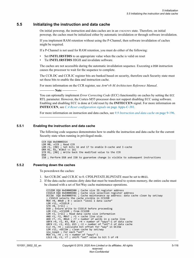
5.5 Initializing the instruction and data cacheOn initial powerup, the instruction and data caches are in an UNKNOWN state. Therefore, on initialpowerup, the caches must be initialized either by automatic invalidation or through software invalidation.
If you implement RAM retention without using the P-Channel, then software invalidation of cachesmight be required.
If a P-Channel is not used for RAM retention, you must do either of the following:
• Set INITL1RSTDIS to an appropriate value when the cache is valid on reset• Tie INITL1RSTDIS HIGH and invalidate software.
The caches are not accessible during the automatic invalidation sequence. Executing a DSB instructioncauses the processor to wait for the sequence to complete.
The CCR.DC and CCR.IC register bits are banked based on security, therefore each Security state mustset these bits to enable the data and instruction cache.
For more information on the CCR register, see Arm®v8-M Architecture Reference Manual. Note
You can optionally implement Error Correcting Code (ECC) functionality on caches by setting the ECCRTL parameter. However, the Cortex-M55 processor does not support disabling ECC using software.Enabling and disabling ECC is done at Cold reset by the INITECCEN signal. For more information onINITECCEN, see C.4 Reset configuration signals on page Appx-C-381.
For more information on instruction and data caches, see 9.9 Instruction and data cache on page 9-196.
5.5.1 Enabling the instruction and data cache
The following code sequence demonstrates how to enable the instruction and data cache for the currentSecurity state when running in privileged mode.
CCR EQU 0xE000ED14LDR R0, =CCR ; Read CCRLDR r1, [R0] ; Set bits 16 and 17 to enable D-cache and I-cacheORR R1, R1, #(0x3 << 16)STR R1, [R0] ; Write back the modified value to the CCRDSBISB ; Perform DSB and ISB to guarantee change is visible to subsequent instructions
5.5.2 Powering down the caches
To powerdown the caches:
1. Set CCR.DC and CCR.IC to 0. CPDLPSTATE.RLPSTATE must be set to 0b11.2. If the data cache contains dirty data that must be transferred to system memory, the entire cache must
be cleaned with a set of Set/Way cache maintenance operations.
CCSIDR EQU 0xE000ED80 ; Cache size ID register addressCSSELR EQU 0xE000ED84 ; Cache size selection register addressDCCSW EQU 0xE000EF6C ; Cache maintenance op address: data cache clean by set/way; CSSELR selects the cache visible in CCSIDRMOV r0, #0x0 ; 0 = select “level 1 data cache”LDR r11, =CSSELR ;STR r0, [r11] ;DSB ; Ensure write to CSSELR before proceedingLDR r11, =CCSIDR ; From CCSIDRLDR r2, [r11] ; Read data cache size informationAND r1, r2, #0x7 ; r1 = cache line sizeADD r7, r1, #0x4 ; r7 = number of words in a cache lineUBFX r4, r2, #3, #10 ; r4 = number of “ways”-1 of data cacheUBFX r2, r2, #13, #15 ; r2 = number of “set”-1 of data cacheCLZ r6, r4 ; calculate bit offset for “way” in DCISWLDR r11, =DCCSW ; clean cache by set/wayinv_loop1 ; For each “set”MOV r1, r4 ; r1 = number of “ways”-1LSLS r8, r2, r7 ; shift “set” value to bit 5 of r8
5 Initialization5.5 Initializing the instruction and data cache
101051_0002_02_en Copyright © 2019, 2020 Arm Limited or its affiliates. All rightsreserved.
5-116
Non-Confidential
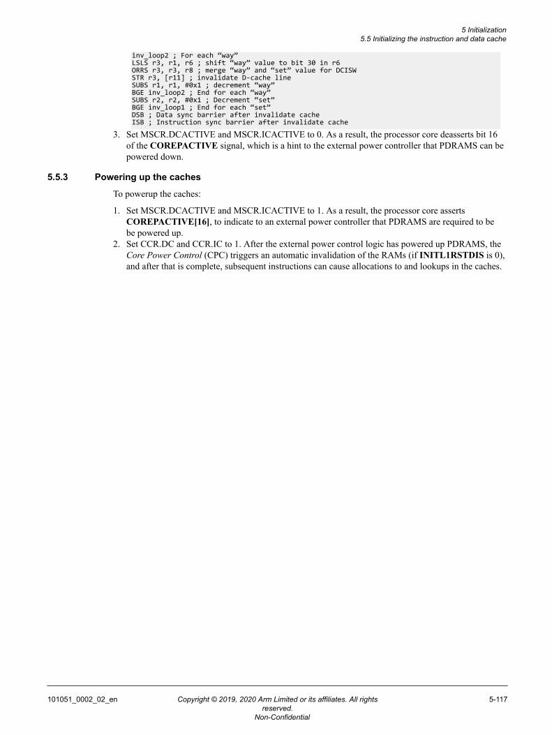
inv_loop2 ; For each “way”LSLS r3, r1, r6 ; shift “way” value to bit 30 in r6ORRS r3, r3, r8 ; merge “way” and “set” value for DCISWSTR r3, [r11] ; invalidate D-cache lineSUBS r1, r1, #0x1 ; decrement “way”BGE inv_loop2 ; End for each “way”SUBS r2, r2, #0x1 ; Decrement “set”BGE inv_loop1 ; End for each “set”DSB ; Data sync barrier after invalidate cacheISB ; Instruction sync barrier after invalidate cache
3. Set MSCR.DCACTIVE and MSCR.ICACTIVE to 0. As a result, the processor core deasserts bit 16of the COREPACTIVE signal, which is a hint to the external power controller that PDRAMS can bepowered down.
5.5.3 Powering up the caches
To powerup the caches:
1. Set MSCR.DCACTIVE and MSCR.ICACTIVE to 1. As a result, the processor core assertsCOREPACTIVE[16], to indicate to an external power controller that PDRAMS are required to bebe powered up.
2. Set CCR.DC and CCR.IC to 1. After the external power control logic has powered up PDRAMS, theCore Power Control (CPC) triggers an automatic invalidation of the RAMs (if INITL1RSTDIS is 0),and after that is complete, subsequent instructions can cause allocations to and lookups in the caches.
5 Initialization5.5 Initializing the instruction and data cache
101051_0002_02_en Copyright © 2019, 2020 Arm Limited or its affiliates. All rightsreserved.
5-117
Non-Confidential
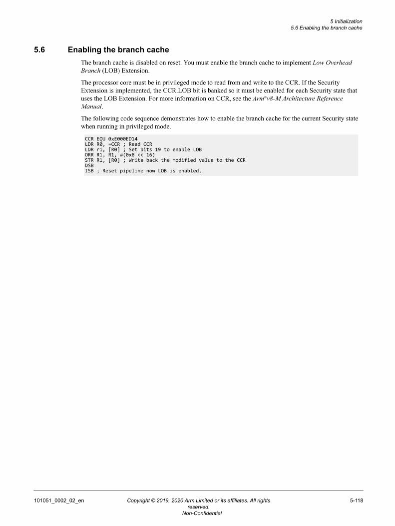
5.6 Enabling the branch cacheThe branch cache is disabled on reset. You must enable the branch cache to implement Low OverheadBranch (LOB) Extension.
The processor core must be in privileged mode to read from and write to the CCR. If the SecurityExtension is implemented, the CCR.LOB bit is banked so it must be enabled for each Security state thatuses the LOB Extension. For more information on CCR, see the Arm®v8-M Architecture ReferenceManual.
The following code sequence demonstrates how to enable the branch cache for the current Security statewhen running in privileged mode.
CCR EQU 0xE000ED14LDR R0, =CCR ; Read CCRLDR r1, [R0] ; Set bits 19 to enable LOBORR R1, R1, #(0x8 << 16)STR R1, [R0] ; Write back the modified value to the CCRDSBISB ; Reset pipeline now LOB is enabled.
5 Initialization5.6 Enabling the branch cache
101051_0002_02_en Copyright © 2019, 2020 Arm Limited or its affiliates. All rightsreserved.
5-118
Non-Confidential
5.7 Enabling and preloading the TCMThe Cortex-M55 processor can optionally include Tightly Coupled Memories (TCMs).
Enabling the TCMs
For more information, see 9.8 TCM interfaces on page 9-192.
Software must set the ITCMCR.EN and DTCMCR.EN fields to enable access to the Instruction TightlyCoupled Memory (ITCM) and Data Tightly Coupled Memory (DTCM) respectively. For moreinformation on these registers, see 4.19 ITCMCR and DTCMCR, TCM Control Registers on page 4-101.
Alternatively, if the INITTCMEN[1:0] signal is asserted on Cold or Warm reset, then software does notneed to write to these registers. For more information on the INITTCMEN[1:0] signal, see C.4 Resetconfiguration signals on page Appx-C-381.
Preloading the TCMs
The methods to preload the TCMs are:
Memory copy with running boot codeWhen boot code includes a memory copy routine that reads data from a ROM and writes it intothe appropriate TCM, you must enable the TCM to perform this operation. This bootcode mustbe run from an address outside the TCM region.
DMA into TCMYou can use a Direct Memory Access (DMA) device that reads data from a ROM and writes it tothe TCMs through the Slave AHB (S-AHB) interface. This method can be used to preload theTCM so they can be used by the processor from reset.
Using the TCM from resetIf the TCM interface is configured to enable the TCMs at reset and the reset vector address isinside the TCM memory region, then the processor boots from TCM. The system must ensurethat the bootcode software is present in the appropriate memory region before execution starts.This can be accomplished by either initializing the memory before reset or by transferring thedata after reset using the S-AHB interface and asserting the CPUWAIT input signal. Assertingthis signal stops the processor fetching or executing instructions after reset. When theCPUWAIT signal is deasserted the processor starts fetching instructions from the reset vectoraddress in the normal way.
Note
Asserting CPUWAIT only takes effect when the processor is under processor reset or Coldreset, that is, nSYSRESET or nPORESET is asserted. The processor does not halt ifCPUWAIT is asserted while the processor is running.
The ITCM and DTCM can be locked from software access using the external input signal, LOCKTCM.When this signal is asserted. it disables writes to registers that are associated with the TCM region fromsoftware or from a debug agent connected to the processor.
• ITCMCR.• DTCMCR.
Asserting this signal prevents changes to the TCM configuration. All writes to the registers are ignored. Note
When ECC is enabled, before performing a byte, halfword, or unaligned word write to a TCM locationwhich causes an RMW, you must initialize the location first by performing an aligned word ordoubleword write to the location. Arm recommends that all TCM locations are initialized in this mannerby boot code.
5 Initialization5.7 Enabling and preloading the TCM
101051_0002_02_en Copyright © 2019, 2020 Arm Limited or its affiliates. All rightsreserved.
5-119
Non-Confidential
5.8 Enabling and locking the TCM security gatesTCM gating is enabled by tying the external input signal CFGMEMALIAS to a non-zero value.
The TCM Gate Unit (TGU) can be locked from software access using the external input signalsLOCKITGU and LOCKDTGU. When these signals are asserted the corresponding TGU registersbecome read-only. This allows a TGU configuration to be programmed and then locked from furtherchanges by software. For more information on TCM security gating, see 8.7 TCM Gate Unitson page 8-164.
5 Initialization5.8 Enabling and locking the TCM security gates
101051_0002_02_en Copyright © 2019, 2020 Arm Limited or its affiliates. All rightsreserved.
5-120
Non-Confidential
5.9 Enabling the P-AHB interfaceSoftware can enable the Peripheral AHB (P-AHB) interface by writing to the PAHBCR.EN register.
For more information on PAHBCR, see 4.14 PAHBCR, P-AHB Control Register on page 4-90.
Alternatively, you can assert INITPAHBEN HIGH at Cold or Warm reset, to enable the P-AHBinterface. If you do this, there is no need for a software write to PAHBCR.EN. For more information onINITPAHBEN, see C.4 Reset configuration signals on page Appx-C-381.
The P-AHB can be locked from software access using the external input signal, LOCKPAHB. Whenthis signal is asserted, writes to PAHBCR register from software or from a debug agent connected to theprocessor are disabled and the register becomes read-only. Asserting this signal prevents changes to P-AHB port enable status in PAHBCR.EN.
5 Initialization5.9 Enabling the P-AHB interface
101051_0002_02_en Copyright © 2019, 2020 Arm Limited or its affiliates. All rightsreserved.
5-121
Non-Confidential

Chapter 6Power management
This chapter introduces Cortex-M55 processor power management concepts.
It contains the following sections:• 6.1 Power domains on page 6-123.• 6.2 Power states on page 6-125.• 6.3 Power and operating mode transitions on page 6-126.• 6.4 Core P-Channel and power mode selection on page 6-130.• 6.5 COREPACTIVE and required power mode on page 6-132.• 6.6 PDCORE low-power requirements on page 6-135.• 6.7 PDEPU low-power requirements on page 6-136.• 6.8 PDRAMS powerdown requirements on page 6-137.• 6.9 Warm reset power mode on page 6-138.• 6.10 Debug Q-Channel and PDDEBUG power domain on page 6-140.• 6.11 Q-Channel clock control on page 6-141.• 6.12 PWRDBGWAKEQACTIVE on page 6-142.
101051_0002_02_en Copyright © 2019, 2020 Arm Limited or its affiliates. All rightsreserved.
6-122
Non-Confidential
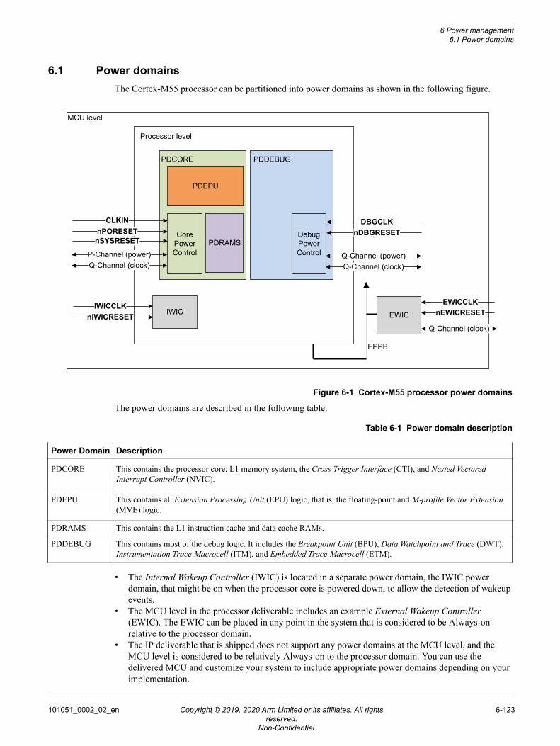
6.1 Power domainsThe Cortex-M55 processor can be partitioned into power domains as shown in the following figure.
MCU level
IWIC
PDEPU
Core Power Control
Processor level
PDCORE PDDEBUG
EWIC
Q-Channel (clock)P-Channel (power)
CLKINnPORESET
nSYSRESETDebug Power Control
Q-Channel (clock)Q-Channel (power)
DBGCLKnDBGRESET
IWICCLKnIWICRESET
EPPB
Q-Channel (clock)
EWICCLKnEWICRESET
PDRAMS
Figure 6-1 Cortex-M55 processor power domains
The power domains are described in the following table.
Table 6-1 Power domain description
Power Domain Description
PDCORE This contains the processor core, L1 memory system, the Cross Trigger Interface (CTI), and Nested VectoredInterrupt Controller (NVIC).
PDEPU This contains all Extension Processing Unit (EPU) logic, that is, the floating-point and M‑profile Vector Extension(MVE) logic.
PDRAMS This contains the L1 instruction cache and data cache RAMs.
PDDEBUG This contains most of the debug logic. It includes the Breakpoint Unit (BPU), Data Watchpoint and Trace (DWT),Instrumentation Trace Macrocell (ITM), and Embedded Trace Macrocell (ETM).
• The Internal Wakeup Controller (IWIC) is located in a separate power domain, the IWIC powerdomain, that might be on when the processor core is powered down, to allow the detection of wakeupevents.
• The MCU level in the processor deliverable includes an example External Wakeup Controller(EWIC). The EWIC can be placed in any point in the system that is considered to be Always-onrelative to the processor domain.
• The IP deliverable that is shipped does not support any power domains at the MCU level, and theMCU level is considered to be relatively Always-on to the processor domain. You can use thedelivered MCU and customize your system to include appropriate power domains depending on yourimplementation.
6 Power management6.1 Power domains
101051_0002_02_en Copyright © 2019, 2020 Arm Limited or its affiliates. All rightsreserved.
6-123
Non-Confidential
Note
For more information on the MCU level, see the Arm® Cortex®-M55 Processor Integration andImplementation Manual. The Arm® Cortex®-M55 Processor Integration and Implementation Manual is aconfidential document that is available to licensees only.
6 Power management6.1 Power domains
101051_0002_02_en Copyright © 2019, 2020 Arm Limited or its affiliates. All rightsreserved.
6-124
Non-Confidential
6.2 Power statesThe power domains in the Cortex-M55 processor can be in ON, OFF, or RET power states. The RETpower state requires the processor logic to be implemented with state retention.
The following table shows the supported power states.
Table 6-2 Supported power states
Power state Clocks running Processor logic powered Register and RAM contents retained Reset asserted
ON Yes/No Yes Yes No
RET No No Yes No
OFF No No No Yes
The following table shows the permitted Cortex-M55 processor power states for the power domains.
Table 6-3 Permitted power states for Cortex-M55 processor power domains
Power state PDCORE PDEPU PDDEBUG PDRAMS
ON Permitted Permitted Permitted Permitted
RET Permitted Permitted Not permitted Permittedb
OFF Permitted Permitted Permitted Permitted
Not all power state combinations are permitted. The combination of PDCORE, PDRAMS, and PDEPUpower states is called the power mode. PDDEBUG is independent of the other power domains. It caneither be ON or OFF, regardless of the processor power mode.
Note
When a power domain is in the ON power state, if the clock is not running, then the domain isconsidered to be in low-power state.
b Retention in the PDRAMS domain is only supported when the processor is in the MEM_RET (Cache), FULL_RET (Cache), or LOGIC_RET (Cache) powermodes.
6 Power management6.2 Power states
101051_0002_02_en Copyright © 2019, 2020 Arm Limited or its affiliates. All rightsreserved.
6-125
Non-Confidential
6.3 Power and operating mode transitionsThe Cortex-M55 processor power modes are based on the Arm standard modes and encodings. Thepower modes are extended with operating modes, which control whether the L1 instruction and datacaches in the PDRAMS domain are enabled.
The Arm standard modes and encodings are defined in the Arm® Power Control System Architecturespecification. The Arm® Power Control System Architecture specification is a confidential document thatis only available to licensees.
An external power controller controls the processor power and operating mode through the P-Channel.An external clock controller controls the Q-Channel allowing system-level clock gating. The P-Channeland the clock control Q-Channel are connected to the Core Power Control (CPC) in the PDCOREdomain. The CPC manages the internal clocking and reset of the PDCORE, PDRAMS, and PDEPUdomains. It supports the clock and reset signals that are described in C.1 Clock and clock enable signalson page Appx-C-377 and C.2 Reset signals on page Appx-C-378, and system-level clock gating. Theprocessor indicates the minimum required power mode according to its state and internal controlregisters using the COREPACTIVE signal. For more information on COREPACTIVE, see C.16 P-Channel and Q-Channel power control signals on page Appx-C-401 and 6.5.1 COREPACTIVE signalencoding on page 6-133.
An external power controller controls the debug power mode through the debug domain power controlQ-Channel. The debug domain power control Q-Channel is connected to the Debug Power Control(DPC) in the PDDEBUG domain. A clock control Q-Channel is also available to support high-levelclock gating.
Only certain transitions between power and operating modes are allowed. Figure 6-2 Permitted powerand operating modes and transitions on page 6-127 shows these permitted transitions. If an externalpower controller request is made to move between two modes which are not directly connected, then therequest is denied (using COREPDENY).
Retention in the PDRAMS domain depends on the overall power and operating mode. RAM retention isselected by entering any of the following:
• MEM_RET (Cache).• FULL_RET (Cache).• LOGIC_RET (Cache).
In other power modes, the PDRAMS state depends on the operating mode.
6 Power management6.3 Power and operating mode transitions
101051_0002_02_en Copyright © 2019, 2020 Arm Limited or its affiliates. All rightsreserved.
6-126
Non-Confidential
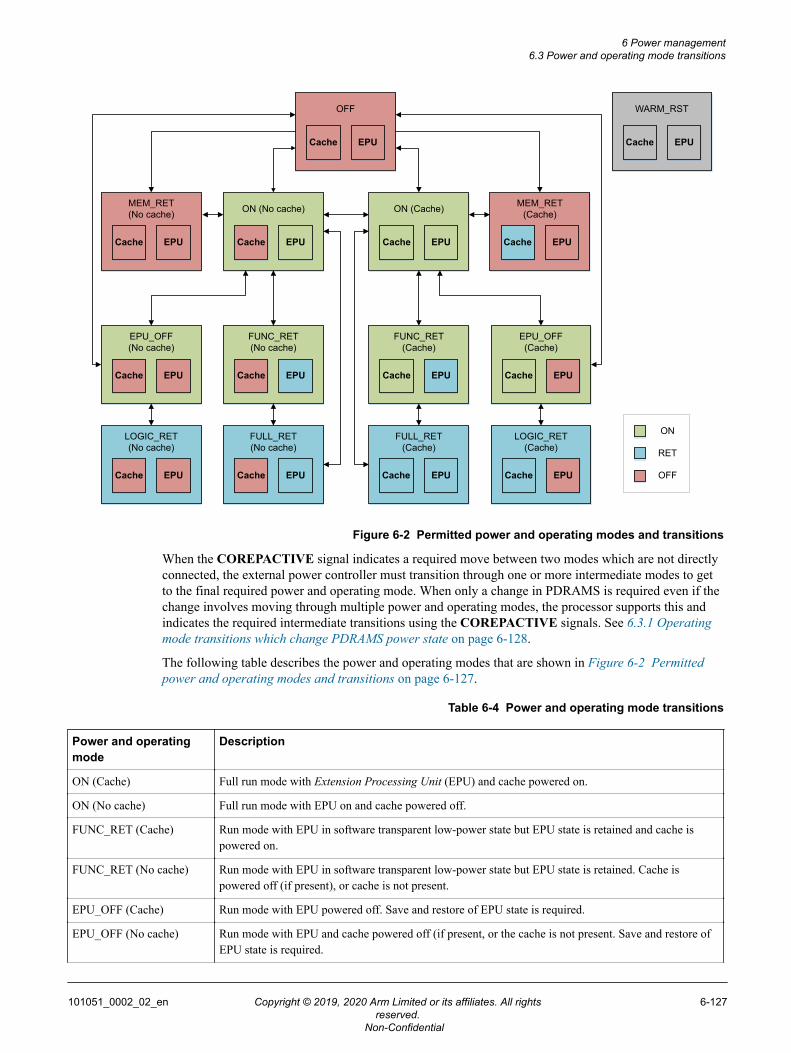
Cache EPU
ON (No cache)
Cache EPU
EPU_OFF (No cache)
Cache EPU
FUNC_RET(No cache)
Cache EPU
LOGIC_RET(No cache)
Cache EPU
FULL_RET(No cache)
Cache EPU
EPU_OFF (Cache)
Cache EPU
FUNC_RET (Cache)
Cache EPU
LOGIC_RET (Cache)
Cache EPU
FULL_RET (Cache)
Cache EPU
ON (Cache)
Cache EPU
OFF
Cache EPU
MEM_RET (Cache)
ON
RET
OFF
Cache EPU
WARM_RST
Cache EPU
MEM_RET (No cache)
Figure 6-2 Permitted power and operating modes and transitions
When the COREPACTIVE signal indicates a required move between two modes which are not directlyconnected, the external power controller must transition through one or more intermediate modes to getto the final required power and operating mode. When only a change in PDRAMS is required even if thechange involves moving through multiple power and operating modes, the processor supports this andindicates the required intermediate transitions using the COREPACTIVE signals. See 6.3.1 Operatingmode transitions which change PDRAMS power state on page 6-128.
The following table describes the power and operating modes that are shown in Figure 6-2 Permittedpower and operating modes and transitions on page 6-127.
Table 6-4 Power and operating mode transitions
Power and operatingmode
Description
ON (Cache) Full run mode with Extension Processing Unit (EPU) and cache powered on.
ON (No cache) Full run mode with EPU on and cache powered off.
FUNC_RET (Cache) Run mode with EPU in software transparent low-power state but EPU state is retained and cache ispowered on.
FUNC_RET (No cache) Run mode with EPU in software transparent low-power state but EPU state is retained. Cache ispowered off (if present), or cache is not present.
EPU_OFF (Cache) Run mode with EPU powered off. Save and restore of EPU state is required.
EPU_OFF (No cache) Run mode with EPU and cache powered off (if present, or the cache is not present. Save and restore ofEPU state is required.
6 Power management6.3 Power and operating mode transitions
101051_0002_02_en Copyright © 2019, 2020 Arm Limited or its affiliates. All rightsreserved.
6-127
Non-Confidential
Table 6-4 Power and operating mode transitions (continued)
Power and operatingmode
Description
FULL_RET (Cache) All functional logic and cache in retention. This is software transparent powerdown.
FULL_RET (No cache) All functional logic in retention with cache powered off (if present), or the cache is not present. This issoftware transparent powerdown.
LOGIC_RET (Cache) This is partially software-transparent powerdown. EPU has been powered off.
LOGIC_RET (No cache) This is partially software-transparent powerdown. EPU has been powered off. Cache is powered off (ifpresent), or cache is not present.
MEM_RET (Cache) All functional logic is powered off, RAMs in retention.
MEM_RET (No cache) MEM_RET (No cache) is functionally identical to OFF. The power mode and associated transitions areincluded for compatibility with the Arm CoreLink™ PCK‑600 Power Control Kit PPU. The Cortex-M55processor never requests this state using the P-Channel COREPACTIVE output signal.
OFF Powered off, Shutdown mode.
WARM_RST Warm reset.
In Table 6-4 Power and operating mode transitions on page 6-127, the No cache operating mode impliesthat if your system configuration includes caches, then the cache is present, but disabled and poweredOFF. The following register bits are set to appropriate values:• MSCR.ICACTIVE and MSCR.DCACTIVE are 0.• CPDLPSTATE.RLPSTATE is 0b11.
Note
• A transition from OFF to MEM_RET is allowed. Arm recommends this as being required for fullcompatibility with the Arm CoreLink PCK‑600 Power Control Kit Power Policy Unit (PPU).Transitions from MEM_RET to OFF are not allowed. The system is responsible for maintainingpower in the RAMs to ensure that processor cache content is preserved when entering MEM_RET.
• A transition from OFF to MEM_RET or MEM_RET to ON does not invalidate the cache even whenINITL1RSTDIS is set to 0.
• MEM_RET (No cache) is functionally identical to OFF. The state and associated transitions areincluded for compatibility with current Arm CoreLink PCK‑600 Power Control Kit Power PolicyUnit (PPU). The Cortex-M55 processor never requests this state using the P-ChannelCOREPACTIVE output signal.
• A request on the P-Channel to transition to the current power mode is always accepted.
6.3.1 Operating mode transitions which change PDRAMS power state
The processor supports transitions between operating modes where the PDRAMS domain is enabled ordisabled.
For example, if the operating mode is ON (No cache) the processor can request to enable PDRAMS.This request results in COREPACTIVE[16] being asserted, requesting a transition to ON (Cache), butthe other bits on COREPACTIVE remain static. The transition between ON (Cache) and ON (Nocache) is called a change of operating mode.
The CoreLink PCK‑600 Power Control Kit only supports dynamic transitions between operating modeswhen in the ON power mode. Therefore, when there is a request to change the operating mode (enable ordisable the cache) for other active power modes like EPU_OFF and FUNC_RET, the processor drivesCOREPACTIVE to ON and the power controller transitions to ON. This allows the operating modetransition to occur. The Core Power Control (CPC) logic includes a secondary state-machine which
6 Power management6.3 Power and operating mode transitions
101051_0002_02_en Copyright © 2019, 2020 Arm Limited or its affiliates. All rightsreserved.
6-128
Non-Confidential
transitions COREPACTIVE through the ON power mode to allow the external power controller toenable or disable PDRAMS.
For example, to transition from EPU_OFF (No cache) to EPU_OFF (Cache) the following steps need totake place. In this example, the processor starts in EPU_OFF(No Cache) mode, with COREPACTIVE[6]set HIGH indicating this is the current minimum required power mode. When the cache is enabled, thefollowing steps need to be followed for the transition to take place:1. The CPC drives COREPACTIVE[8] and COREPACTIVE[16] HIGH.2. The external power controller responds with COREPREQ and COREPSTATE = ON (No cache).
COREPACTIVE[16] is ignored because an operating mode transition cannot occur unless the powermode is ON.
3. The processor transitions the power mode from EPU_OFF (No cache) to ON (No cache).4. The CPC continues to drive COREPACTIVE[8] and COREPACTIVE[16] HIGH.5. The external power controller responds with COREPREQ and COREPSTATE = ON (Cache), and
requests a change in operating mode in the ON power mode.6. The processor transitions the power mode from ON (No cache) to ON (Cache).7. The CPC deasserts COREPACTIVE[8], meaning COREPACTIVE[6] is now the highest
COREPACTIVE bit set and the minimum required power mode.8. The external power controller responds with COREPREQ and COREPSTATE = EPU_OFF
(Cache).9. The processor transitions the power mode from ON (Cache) to EPU_OFF (Cache) and continues to
assert COREPACTIVE[6] and COREPACTIVE[16] HIGH. Tip
For more information on the COREPACTIVE output signal encoding, see 6.5.1 COREPACTIVEsignal encoding on page 6-133.
6 Power management6.3 Power and operating mode transitions
101051_0002_02_en Copyright © 2019, 2020 Arm Limited or its affiliates. All rightsreserved.
6-129
Non-Confidential
6.4 Core P-Channel and power mode selectionThe power modes are based on the power state of the PDCORE, PDEPU, and PDRAMS domains.
The requested power mode is defined according to the lowest achievable mode based on the processorlogic state, external conditions, and the corresponding CPDLPSTATE register fields. The resulting powermode is driven on the P-Channel COREPACTIVE output signal.
Tip
For more information on COREPACTIVE signal encoding, see 6.5.1 COREPACTIVE signalencoding on page 6-133.
The following table shows the resultant overall power mode that is based on the requests from eachindividual processor power domain.
Table 6-5 Requested domain power states and resultant power and operating mode
Requested domain power states Resultant power and operating mode
PDCORE PDEPU PDRAMS
ON ON ON ON (Cache)
ON ON OFF ON (No cache)
ON RET ON FUNC_RET (Cache)
ON RET OFF FUNC_RET (No cache)
ON OFF ON EPU_OFF (Cache)
ON OFF OFF EPU_OFF (No cache)
RET RET/ON ON FULL_RET (Cache)
RET RET/ON OFF FULL_RET (No cache)
RET OFF ON LOGIC_RET (Cache)
RET OFF OFF LOGIC_RET (No cache)
OFF ON ON ON (Cache)
OFF ON OFF ON (No cache)
OFF RET ON FULL_RET (Cache)
OFF RET OFF FULL_RET (No cache)
OFF OFF ON MEM_RET (Cache)
OFF OFF OFF OFF
- - - WARM_RST
Some combinations of power domain states do not map directly onto a power mode:
• Requesting ON for PDEPU when PDCORE is RET always results in a power mode with the EPU inretention.
• If PDEPU is required to be ON or RET, the selected power mode always retains EPU state.• The lowest possible power mode is selected which matches the requested PDRAMS power state.
At Cold reset, the internal power mode is OFF and the P-Channel COREPACTIVE signal is also drivenOFF. Before fetching the reset vector or starting to execute instructions, the processor waits for thesystem to request or initialize an operational state for the PDCORE domain.
6 Power management6.4 Core P-Channel and power mode selection
101051_0002_02_en Copyright © 2019, 2020 Arm Limited or its affiliates. All rightsreserved.
6-130
Non-Confidential
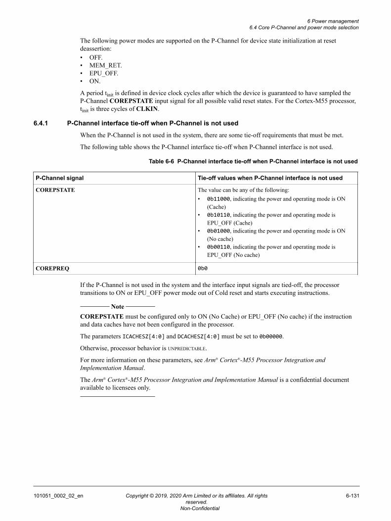
The following power modes are supported on the P-Channel for device state initialization at resetdeassertion:• OFF.• MEM_RET.• EPU_OFF.• ON.
A period tinit is defined in device clock cycles after which the device is guaranteed to have sampled theP-Channel COREPSTATE input signal for all possible valid reset states. For the Cortex-M55 processor,tinit is three cycles of CLKIN.
6.4.1 P-Channel interface tie-off when P-Channel is not used
When the P-Channel is not used in the system, there are some tie-off requirements that must be met.
The following table shows the P-Channel interface tie-off when P-Channel interface is not used.
Table 6-6 P-Channel interface tie-off when P-Channel interface is not used
P-Channel signal Tie-off values when P-Channel interface is not used
COREPSTATE The value can be any of the following:• 0b11000, indicating the power and operating mode is ON
(Cache)• 0b10110, indicating the power and operating mode is
EPU_OFF (Cache)• 0b01000, indicating the power and operating mode is ON
(No cache)• 0b00110, indicating the power and operating mode is
EPU_OFF (No cache)
COREPREQ 0b0
If the P-Channel is not used in the system and the interface input signals are tied-off, the processortransitions to ON or EPU_OFF power mode out of Cold reset and starts executing instructions.
Note
COREPSTATE must be configured only to ON (No Cache) or EPU_OFF (No cache) if the instructionand data caches have not been configured in the processor.
The parameters ICACHESZ[4:0] and DCACHESZ[4:0] must be set to 0b00000.
Otherwise, processor behavior is UNPREDICTABLE.
For more information on these parameters, see Arm® Cortex®-M55 Processor Integration andImplementation Manual.
The Arm® Cortex®-M55 Processor Integration and Implementation Manual is a confidential documentavailable to licensees only.
6 Power management6.4 Core P-Channel and power mode selection
101051_0002_02_en Copyright © 2019, 2020 Arm Limited or its affiliates. All rightsreserved.
6-131
Non-Confidential
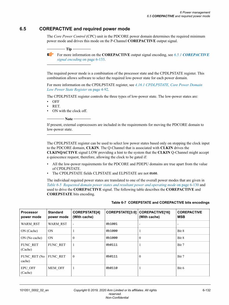
6.5 COREPACTIVE and required power modeThe Core Power Control (CPC) unit in the PDCORE power domain determines the required minimumpower mode and drives this mode on the P-Channel COREPACTIVE output signal.
Tip
For more information on the COREPACTIVE output signal encoding, see 6.5.1 COREPACTIVEsignal encoding on page 6-133.
The required power mode is a combination of the processor state and the CPDLPSTATE register. Thiscombination allows software to select the required low-power state for each power domain.
For more information on the CPDLPSTATE register, see 4.16.1 CPDLPSTATE, Core Power DomainLow Power State Register on page 4-92.
The CPDLPSTATE register controls the three types of low-power state. The low-power states are:• OFF• RET.• ON with the clock off.
Note
If present, external coprocessors are included in the requirements for moving the PDCORE domain tolow-power state.
The CPDLPSTATE register can be used to select low power states based only on stopping the clock inputto the PDCORE domain, CLKIN. The Q-Channel that is associated with CLKIN drives theCLKINQACTIVE signal LOW providing a hint to the system that the CLKIN Q-Channel might accepta quiescence request, therefore, allowing the clock to be gated if:
• All the low-power requirements for the PDCORE and PDEPU domains are true apart from the valueof CPDLPSTATE.
• The CPDLPSTATE fields CLPSTATE and ELPSTATE are not 0b00.
The individual required power states are translated to one of the overall power modes that are given inTable 6-5 Requested domain power states and resultant power and operating mode on page 6-130 andused to drive the COREPACTIVE signal. The following table describes the COREPACTIVE andCOREPSTATE bits encoding.
Table 6-7 COREPSTATE and COREPACTIVE bits encodings
Processorpower mode
Standardpower mode
COREPSTATE[4](With cache)
COREPSTATE[3:0] COREPACTIVE[16](With cache)
COREPACTIVEMSB
WARM_RST WARM_RST - 0b1001 - -
ON (Cache) ON 1 0b1000 1 Bit 8
ON (No cache) ON 0 0b1000 0 Bit 8
FUNC_RET(Cache)
FUNC_RET 1 0b0111 1 Bit 7
FUNC_RET (Nocache)
FUNC_RET 0 0b0111 0 Bit 7
EPU_OFF(Cache)
MEM_OFF 1 0b0110 1 Bit 6
6 Power management6.5 COREPACTIVE and required power mode
101051_0002_02_en Copyright © 2019, 2020 Arm Limited or its affiliates. All rightsreserved.
6-132
Non-Confidential
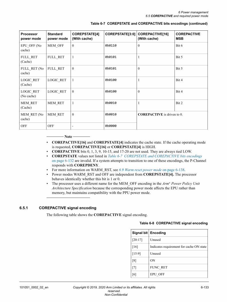
Table 6-7 COREPSTATE and COREPACTIVE bits encodings (continued)
Processorpower mode
Standardpower mode
COREPSTATE[4](With cache)
COREPSTATE[3:0] COREPACTIVE[16](With cache)
COREPACTIVEMSB
EPU_OFF (Nocache)
MEM_OFF 0 0b0110 0 Bit 6
FULL_RET(Cache)
FULL_RET 1 0b0101 1 Bit 5
FULL_RET (Nocache)
FULL_RET 0 0b0101 0 Bit 5
LOGIC_RET(Cache)
LOGIC_RET 1 0b0100 1 Bit 4
LOGIC_RET(No cache)
LOGIC_RET 0 0b0100 0 Bit 4
MEM_RET(Cache)
MEM_RET 1 0b0010 1 Bit 2
MEM_RET (Nocache)
MEM_RET 0 0b0010 COREPACTIVE is driven to 0.
OFF OFF - 0b0000
Note
• COREPACTIVE[16] and COREPSTATE[4] indicates the cache state. If the cache operating modeis requested, COREPACTIVE[16] or COREPSTATE[4] is HIGH.
• COREPACTIVE bits 0, 1, 3, 9, 10-15, and 17-20 are not used. They are always tied LOW.• COREPSTATE values not listed in Table 6-7 COREPSTATE and COREPACTIVE bits encodings
on page 6-132 are invalid. If a system attempts to transition to one of these encodings, the P-Channelresponds with COREPDENY.
• For more information on WARM_RST, see 6.9 Warm reset power mode on page 6-138.• Power modes WARM_RST and OFF are independent from COREPSTATE[4]. The processor
behaves identically whether this bit is 1 or 0.• The processor uses a different name for the MEM_OFF encoding in the Arm® Power Policy Unit
Architecture Specification because the corresponding power mode affects the EPU rather thanmemory, but maintains compatibility with the PPU power mode.
6.5.1 COREPACTIVE signal encoding
The following table shows the COREPACTIVE signal encoding.
Table 6-8 COREPACTIVE signal encoding
Signal bit Encoding
[20:17] Unused
[16] Indicates requirement for cache ON state
[15:9] Unused
[8] ON
[7] FUNC_RET
[6] EPU_OFF
6 Power management6.5 COREPACTIVE and required power mode
101051_0002_02_en Copyright © 2019, 2020 Arm Limited or its affiliates. All rightsreserved.
6-133
Non-Confidential
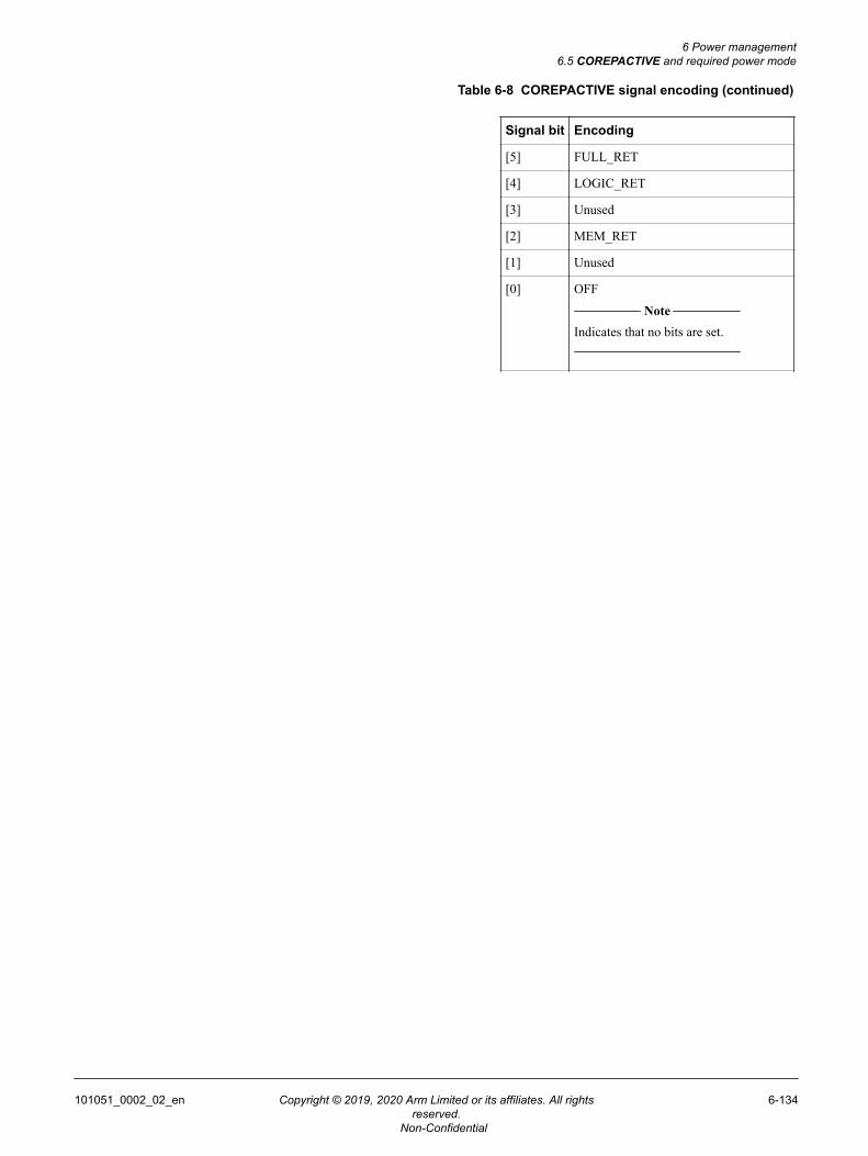
Table 6-8 COREPACTIVE signal encoding (continued)
Signal bit Encoding
[5] FULL_RET
[4] LOGIC_RET
[3] Unused
[2] MEM_RET
[1] Unused
[0] OFF Note
Indicates that no bits are set.
6 Power management6.5 COREPACTIVE and required power mode
101051_0002_02_en Copyright © 2019, 2020 Arm Limited or its affiliates. All rightsreserved.
6-134
Non-Confidential
6.6 PDCORE low-power requirementsThe following conditions must be true to request a PDCORE low-power state on the COREPACTIVEsignal using the P-Channel:
• The processor is in sleep mode.• SCR.SLEEPDEEP is set.• WICCONTROL[0] is asserted so that DEEPSLEEP means Wakeup Interrupt Controller (WIC)
sleep.• If External Wakeup Interrupt Controller (EWIC) is configured, any automatic WIC loading must be
completed.• The Slave AHB (S-AHB) interface is inactive.• The Debug AHB (D-AHB) interface is inactive.• The core is not halted.• CPDLPSTATE.CLPSTATE is equal to 0b10 or 0b11.• No MBIST operation is in progress.• The CTI is not included or disabled, or if the CTI is included and enabled, there is no valid mapping
that is set up for an external cross trigger to be passed onto the processor, or CTI integration mode isenabled in CTI_ITCONTROL .
When the PDCORE low-power requirements are met, CPDLPSTATE.CLPSTATE selects the low-powerstate.
Note
• If the Security Extension is included in the processor:— The input signal, CPSPRESENT[n] indicates that coprocessor n is included— CPACR_S.CPn and CPACR_NS.CPn indicate that coprocessor n is enabled and needs power.
If the Security Extension is not included in the processor:— The input signal, CPNSPRESENT[n] indicates that coprocessor n is included— CPACR_NS.CPn indicates that coprocessor n is enabled and needs power.
For more information on CPACR, see the Arm®v8-M Architecture Reference Manual.• If a coprocessor CPn that is included in the system is indicating that the state cannot be lost
(CPSPRESENT[n]&&CPPWR.SUn=0b0), then a request to powerdown inCPDLPSTATE.CLPSTATE is converted to RET to preserve the coprocessor state. For moreinformation on CPPWR, see the Arm®v8-M Architecture Reference Manual.
• To request a PDCORE low-power state using clock gating only, CPDLPSTATE.CLPSTATE must be0b01.
6 Power management6.6 PDCORE low-power requirements
101051_0002_02_en Copyright © 2019, 2020 Arm Limited or its affiliates. All rightsreserved.
6-135
Non-Confidential
6.7 PDEPU low-power requirementsThe following conditions must be true to request a PDEPU low-power state on the COREPACTIVEsignal using the P-Channel:
• The processor core is not halted.• There are no scalar floating-point or M-profile Vector Extension (MVE) instructions in progress.• CPDLPSTATE.ELPSTATE is equal to 0b10 or 0b11.
When the PDEPU low-power requirements are met, CPDLPSTATE.ELPSTATE selects the low-powerstate.
Note
• If CPPWR.SU10 is 0b0, then selecting OFF in CPDLPSTATE.ELPSTATE results in RET state beingselected to prevent the state from becoming UNKNOWN. For more information on CPPWR, see theArm®v8-M Architecture Reference Manual.
• To request a PDEPU low-power state using clock gating only, CPDLPSTATE.ELPSTATE must be0b01.
6 Power management6.7 PDEPU low-power requirements
101051_0002_02_en Copyright © 2019, 2020 Arm Limited or its affiliates. All rightsreserved.
6-136
Non-Confidential
6.8 PDRAMS powerdown requirementsThe following conditions must be true to powerdown PDRAMS:
• MSCR.DCACTIVE is equal to 0b0. This field is ignored for transparent retention of the RAMs.• MSCR.ICACTIVE is equal to 0b0. This field is ignored for transparent retention of the RAMs.• CPDLPSTATE.RLPSTATE is equal to 0b11.• No cache maintenance operation is in progress.• Automatic cache invalidation is not in progress.• No MBIST operation is in progress to the instruction cache or data cache.
6 Power management6.8 PDRAMS powerdown requirements
101051_0002_02_en Copyright © 2019, 2020 Arm Limited or its affiliates. All rightsreserved.
6-137
Non-Confidential
6.9 Warm reset power modeThe WARM_RST power mode is used when external control logic requires the processor to be put in asafe state for Warm reset.
Asserting nSYSRESET when the PDCORE is powered off or in a retention state, or if the EPU ispowered off or in retention state (power modes OFF, EPU_OFF, MEM_RET, LOGIC_RET, FUNC_RET,or FULL RET) has an UNPREDICTABLE effect on the operation of the processor.
Asserting nSYSRESET when PDCORE is in an active state and not in WARM_RST state might resultin system deadlock.
Entering WARM_RST
WARM_RST can only be entered from the ON power mode. Requesting WARM_RST from any otherpower mode results in COREPDENY being asserted.
The processor asserts COREPACCEPT when PDCORE is transitioning to a quiescent state, and is heldasserted until core quiescence is achieved. Therefore, it is only safe to assert nSYSRESET after the P-Channel transition to WARM_RST is completed.
This core quiescence requires that there are no outstanding transactions on the Master-AXI (M-AXI),Peripheral AHB (P-AHB), External Private Peripheral Bus (EPPB), Debug AHB (D-AHB) and SlaveAHB (S-AHB) interfaces. If a request is made on the S-AHB interface while the processor is inWARM_RST power mode it is ignored. Therefore, the system is responsible for ensuring that noaccesses are made on the S-AHB slave interface until the processor leaves WARM_RST whether or notreset is asserted in the power mode.
If a debug access is made on D-AHB while in WARM_RST it is captured on the slave interface andpended until the power mode is switched back out of WARM_RST, at which point the access is made tothe processor. If the D-AHB access is to state which has been reset while in WARM_RST then the resultcould be UNPREDICTABLE.
The processor ensures that all the outputs of the PDCORE domain are set to their reset values. Therefore,when nSYSRESET is asserted these values do not change, which helps to prevent reset domain crossingissues.
In particular, the AIRCR.SYSRESETREQ is cleared on entry to WARM_RST, so that theSYSRESETREQ output signal is driven to 0 matching the reset condition.
Warm reset can always be applied safely when the processor is in a low-power sleep state with all powerdomains powered-on and no requests are active on the S-AHB or D-AHB interfaces.
If your system has a P-Channel interface for power control, then it is only safe to assert nSYSRESETwhen the processor is in any of the following modes:• WARM_RST, which is advantageous because it does not require software support• OFF• MEM_RET
If your system does not use a P-Channel interface for power control, then Arm recommends that youassert nSYSRESET when the processor core is in sleep mode, all the power domains are powered up,and there are no S-AHB or D-AHB requests.
The Warm reset request does not require that any of the power domains change power state. Thecombination of power states remains unchanged from when the processor entered the WARM_RSTpower mode.
Exiting WARM_RST
The processor can exit WARM_RST mode, whether or not nSYSRESET has been asserted to reset thePDCORE power domain. If no reset has occurred program execution continues from where it was beforeWARM_RST was requested. The processor asserts COREPACCEPT for any request to transition from
6 Power management6.9 Warm reset power mode
101051_0002_02_en Copyright © 2019, 2020 Arm Limited or its affiliates. All rightsreserved.
6-138
Non-Confidential
WARM_RST to the ON and FUNC_RET power modes. Requests to transition from WARM_RST to anyother power mode results in COREPDENY being asserted.
The WARM_RST request does not require that any of the power domains change power state. Thecombination of power states when in the WARM_RST power mode will be the same as before it enteredthat power mode. The COREPACTIVE output signal will remain the same value as it was beforeCOREPACCEPT was asserted for COREPSTATE indicating WARM_RST entry.
Note
The Cortex-M55 processor has internal logic that deals with any metastability caused by either of thefollowing asynchronous resets:• Asserting nSYSRESET while the processor core is in the WARM_RST, OFF, or MEM_RET power
modes.• Resetting any power domain because of entry to a power state that is controlled by the P-Channel or
Q-Channel.
6 Power management6.9 Warm reset power mode
101051_0002_02_en Copyright © 2019, 2020 Arm Limited or its affiliates. All rightsreserved.
6-139
Non-Confidential
6.10 Debug Q-Channel and PDDEBUG power domainA Q-Channel interface controls the PDDEBUG power domain.
The PDDEBUG power domain logic drives the PWRDBGQACTIVE signal HIGH to indicate that thedomain is active if any of the following conditions are met:• Trace is enabled, DEMCR.TRCENA=1.• If configured, the Embedded Trace Macrocell (ETM) is enabled, TRCPDCR.PU=1.• There is outstanding trace data in the ETM, Instrumentation Trace Macrocell (ITM), or Data
Watchpoint and Trace (DWT).• There is an outstanding access to any of the registers in PDDEBUG from software or from a debug
request on Debug AHB (D-AHB).• The BreakPoint Unit (BPU) is enabled, FP_CTRL.ENABLE=1.• DPDLPSTATE.DLPSTATE is 0b00 or 0b01.
Note
• Setting DPDLPSTATE.DLPSTATE to 0b01 indicates that DBGCLK can be gated when the domainis idle. This results in the DBGCLKQACTIVE signal being set LOW when the PDDEBUG domainis idle.
• For more information on the DPDLPSTATE register, see 4.16.2 DPDLPSTATE, Debug PowerDomain Low Power State Register on page 4-93.
• For more information on TRCPDCR, see Arm® CoreSight™ ETM‑M55 Technical Reference Manual.• For more information on the FP_CTRL and DEMCR, see the Arm®v8-M Architecture Reference
Manual.• For more information on the Q-Channel interface and its signals, see the AMBA® Low Power
Interface Specification Arm® Q-Channel and P-Channel Interfaces.
6 Power management6.10 Debug Q-Channel and PDDEBUG power domain
101051_0002_02_en Copyright © 2019, 2020 Arm Limited or its affiliates. All rightsreserved.
6-140
Non-Confidential
6.11 Q-Channel clock controlTo optimize power usage, the Cortex-M55 processor includes Q-Channel interfaces which allow thesystem to gate the clocks that are associated with the PDCORE and PDDEBUG power domains at a highlevel in the clock tree.
The PDCORE clock signal, CLKIN, is controlled using:
• CLKINQREQn.• CLKINQACCEPTn.• CLKINQDENY.• CLKINQACTIVE.
The PDDEBUG clock signal, DBGCLK, is controlled using:
• DBGCLKQREQn.• DBGCLKQACCEPTn.• DBGCLKQDENY.• DBGCLKQACTIVE.
The following rules apply for PDCORE and PDDEBUG clock signals:• If both CLKIN and DBGCLK are running, they must be fully synchronous to each other.• CLKINQACTIVE is asserted when PDCORE requires a clock.• DBGCLKQACTIVE is asserted when PDDEBUG requires a clock.• CLKIN can only be gated when its clock control Q-Channel is in the Q_STOPPED state or when the
PDCORE P-Channel is in LOGIC_RET, FULL_RET, MEM_RET, or OFF.• DBGCLK can only be gated when its clock control Q-Channel is in Q_STOPPED state or when the
PDDEBUG power control Q-Channel is in Q_STOPPED.
6 Power management6.11 Q-Channel clock control
101051_0002_02_en Copyright © 2019, 2020 Arm Limited or its affiliates. All rightsreserved.
6-141
Non-Confidential
6.12 PWRDBGWAKEQACTIVEThe PDCORE domain asserts the PWRDBGWAKEQACTIVE output signal for the following cases.
• When there is an access to a register located in the PDDEBUG domain, either from software runningon the processor or from a request on the Debug AHB (D-AHB) interface.
• When there is a request to any EPPB address which is not a part of the External Wakeup InterruptController (EWIC) address space starting from 0xE0047000.
This signal must be routed to the external power controller and used to power up the PDDEBUG domain.The processor uses an internal signal to determine when the debug domain is active and when it is safe toperform the access. The PWRDBGWAKEQACTIVE signal can be OR gated with thePWRDBGQACTIVE signal to indicate to the external power controller that the PDDEBUG domainmust be activated.
6 Power management6.12 PWRDBGWAKEQACTIVE
101051_0002_02_en Copyright © 2019, 2020 Arm Limited or its affiliates. All rightsreserved.
6-142
Non-Confidential

Chapter 7Memory model
This chapter describes the Cortex-M55 processor memory model.
It contains the following sections:• 7.1 Memory map on page 7-144.• 7.2 Memory types on page 7-146.• 7.3 Private Peripheral Bus on page 7-148.• 7.4 Unaligned accesses on page 7-150.• 7.5 Access privilege level for Device and Normal memory on page 7-152.• 7.6 Memory ordering and barriers on page 7-153.• 7.7 Execute Only Memory on page 7-154.
101051_0002_02_en Copyright © 2019, 2020 Arm Limited or its affiliates. All rightsreserved.
7-143
Non-Confidential
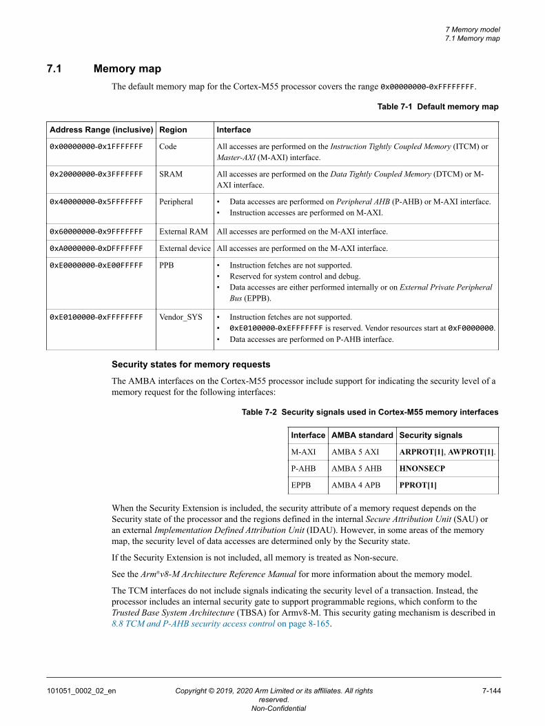
7.1 Memory mapThe default memory map for the Cortex-M55 processor covers the range 0x00000000-0xFFFFFFFF.
Table 7-1 Default memory map
Address Range (inclusive) Region Interface
0x00000000-0x1FFFFFFF Code All accesses are performed on the Instruction Tightly Coupled Memory (ITCM) orMaster-AXI (M-AXI) interface.
0x20000000-0x3FFFFFFF SRAM All accesses are performed on the Data Tightly Coupled Memory (DTCM) or M-AXI interface.
0x40000000-0x5FFFFFFF Peripheral • Data accesses are performed on Peripheral AHB (P-AHB) or M-AXI interface.• Instruction accesses are performed on M-AXI.
0x60000000-0x9FFFFFFF External RAM All accesses are performed on the M-AXI interface.
0xA0000000-0xDFFFFFFF External device All accesses are performed on the M-AXI interface.
0xE0000000-0xE00FFFFF PPB • Instruction fetches are not supported.• Reserved for system control and debug.• Data accesses are either performed internally or on External Private Peripheral
Bus (EPPB).
0xE0100000-0xFFFFFFFF Vendor_SYS • Instruction fetches are not supported.• 0xE0100000-0xEFFFFFFF is reserved. Vendor resources start at 0xF0000000.• Data accesses are performed on P-AHB interface.
Security states for memory requests
The AMBA interfaces on the Cortex-M55 processor include support for indicating the security level of amemory request for the following interfaces:
Table 7-2 Security signals used in Cortex-M55 memory interfaces
Interface AMBA standard Security signals
M-AXI AMBA 5 AXI ARPROT[1], AWPROT[1].
P-AHB AMBA 5 AHB HNONSECP
EPPB AMBA 4 APB PPROT[1]
When the Security Extension is included, the security attribute of a memory request depends on theSecurity state of the processor and the regions defined in the internal Secure Attribution Unit (SAU) oran external Implementation Defined Attribution Unit (IDAU). However, in some areas of the memorymap, the security level of data accesses are determined only by the Security state.
If the Security Extension is not included, all memory is treated as Non-secure.
See the Arm®v8-M Architecture Reference Manual for more information about the memory model.
The TCM interfaces do not include signals indicating the security level of a transaction. Instead, theprocessor includes an internal security gate to support programmable regions, which conform to theTrusted Base System Architecture (TBSA) for Armv8‑M. This security gating mechanism is described in8.8 TCM and P-AHB security access control on page 8-165.
7 Memory model7.1 Memory map
101051_0002_02_en Copyright © 2019, 2020 Arm Limited or its affiliates. All rightsreserved.
7-144
Non-Confidential

Bit-banding
This feature is not supported on the Cortex-M55 processor unless your system includes additionalhardware to perform the appropriate mapping. If bit-banding support is required, Arm recommends thatperipherals are memory mapped to alias their bits to byte, halfword, or words.
7 Memory model7.1 Memory map
101051_0002_02_en Copyright © 2019, 2020 Arm Limited or its affiliates. All rightsreserved.
7-145
Non-Confidential
7.2 Memory typesEach address in the memory map has a memory type which is determined by the default memory map orthe Memory Protection Unit (MPU).
The memory types are:
Normal memoryBy default, half of the memory space is classified as Normal memory. Normal memory hasmany attributes, including Cacheability (Non-cacheable, Write-Through Cacheable, Write-BackCacheable) and Shareability (Inner Shareability and outer Shareability), that impacts how datacan be used in the system. Unaligned accesses to this memory type are allowed. However, undersoftware control, the processor can fault on Unaligned accesses to Normal memory.
Device memoryDevice memory is not idempotent and it is generally used by peripherals.Architecturally, memory locations that are idempotent have the following properties:• Read accesses can be repeated with no side-effects.• Repeated read accesses return the last value that is written to the resource being read.• Read accesses can fetch additional memory locations with no side-effects.• Write accesses can be repeated with no side-effects, if the contents of the location that is
accessed are unchanged between the repeated writes or as the result of an exception.• Unaligned accesses can be supported.• Accesses can be merged before accessing the target memory system.
For more information, see the Arm®v8-M Architecture Reference Manual.There are restrictions on how Device memory can be ordered, merged, or speculated. Theserestrictions subdivide Device memory into the following subtypes.
Gathering, G and nGGathering, G, is the capability to gather and merge requests together into a singletransaction. nG represents the non-Gathering attribute.
Reordering, R and nRReordering, R, is the capability to reorder transactions. nR represents the non-Reordering attribute.
Early Write Acknowledgment, E and nEEarly Write Acknowledgment, E, is the capability to accept early acknowledgment oftransactions from the interconnect. nE represents the non-Early WriteAcknowledgement attribute, indicating that buffering is not permitted. For the Cortex-M55 processor, nE Device transactions are buffered inside the processor itself. Thisattribute is then passed to the external interface to ensure that the response is receivedappropriately.
The Cortex-M55 processor treats the different types of Device memory identically. However, for MVEinstructions, regardless of the Gathering attribute, multiple requests might be merged into onetransaction. For Device memory:• Data accesses are coherent for all system observers.• All accesses must be aligned to the data type specified in the instruction. Unaligned accesses generate
an Alignment fault.
RemappingThe default memory map defines the Peripheral, External device, PPB, and Vendor_SYS regions asDevice and the rest of the memory regions as Normal.• Normal memory can be changed to Device.• Device memory can be changed to Normal except for the following cases.
7 Memory model7.2 Memory types
101051_0002_02_en Copyright © 2019, 2020 Arm Limited or its affiliates. All rightsreserved.
7-146
Non-Confidential

— The PPB region is always Device-nGnRnE.— The Vendor_SYS region is Device-nGnRE and can be changed to Device-nGnRnE.— Mapping the Vendor_SYS region from Device to Normal results in UNPREDICTABLE behavior.
For more information on memory types and their attributes, see the Arm®v8-M Architecture ReferenceManual.
7 Memory model7.2 Memory types
101051_0002_02_en Copyright © 2019, 2020 Arm Limited or its affiliates. All rightsreserved.
7-147
Non-Confidential
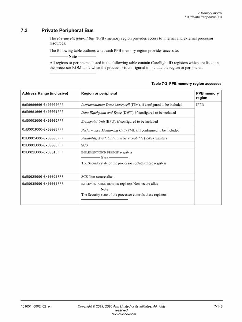
7.3 Private Peripheral BusThe Private Peripheral Bus (PPB) memory region provides access to internal and external processorresources.
The following table outlines what each PPB memory region provides access to. Note
All regions or peripherals listed in the following table contain CoreSight ID registers which are listed inthe processor ROM table when the processor is configured to include the region or peripheral.
Table 7-3 PPB memory region accesses
Address Range (inclusive) Region or peripheral PPB memoryregion
0xE0000000-0xE0000FFF Instrumentation Trace Macrocell (ITM), if configured to be included IPPB
0xE0001000-0xE0001FFF Data Watchpoint and Trace (DWT), if configured to be included
0xE0002000-0xE0002FFF Breakpoint Unit (BPU), if configured to be included
0xE0003000-0xE0003FFF Performance Monitoring Unit (PMU), if configured to be included
0xE0005000-0xE0005FFF Reliability, Availability, and Serviceability (RAS) registers
0xE000E000-0xE000EFFF SCS
0xE001E000-0xE001EFFF IMPLEMENTATION DEFINED registers Note
The Security state of the processor controls these registers.
0xE002E000-0xE002EFFF SCS Non-secure alias
0xE003E000-0xE003EFFF IMPLEMENTATION DEFINED registers Non-secure alias Note
The Security state of the processor controls these registers.
7 Memory model7.3 Private Peripheral Bus
101051_0002_02_en Copyright © 2019, 2020 Arm Limited or its affiliates. All rightsreserved.
7-148
Non-Confidential
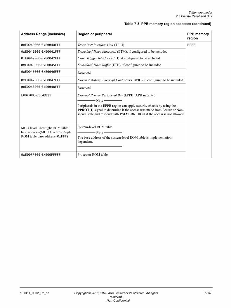
Table 7-3 PPB memory region accesses (continued)
Address Range (inclusive) Region or peripheral PPB memoryregion
0xE0040000-0xE0040FFF Trace Port Interface Unit (TPIU) EPPB
0xE0041000-0xE0041FFF Embedded Trace Macrocell (ETM), if configured to be included
0xE0042000-0xE0042FFF Cross Trigger Interface (CTI), if configured to be included
0xE0045000-0xE0045FFF Embedded Trace Buffer (ETB), if configured to be included
0xE0046000-0xE0046FFF Reserved
0xE0047000-0xE0047FFF External Wakeup Interrupt Controller (EWIC), if configured to be included
0xE0048000-0xE0048FFF Reserved
E0049000-E0049FFF External Private Peripheral Bus (EPPB) APB interface Note
Peripherals in the EPPB region can apply security checks by using thePPROT[1] signal to determine if the access was made from Secure or Non-secure state and respond with PSLVERR HIGH if the access is not allowed.
MCU level CoreSight ROM tablebase address-(MCU level CoreSightROM table base address+0xFFF)
System-level ROM table Note
The base address of the system-level ROM table is implementation-dependent.
0xE00FF000-0xE00FFFFF Processor ROM table
7 Memory model7.3 Private Peripheral Bus
101051_0002_02_en Copyright © 2019, 2020 Arm Limited or its affiliates. All rightsreserved.
7-149
Non-Confidential
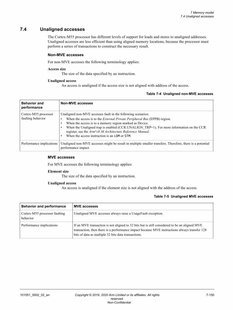
7.4 Unaligned accessesThe Cortex-M55 processor has different levels of support for loads and stores to unaligned addresses.Unaligned accesses are less efficient than using aligned memory locations, because the processor mustperform a series of transactions to construct the necessary result.
Non-MVE accesses
For non-MVE accesses the following terminology applies:
Access sizeThe size of the data specified by an instruction.
Unaligned accessAn access is unaligned if the access size is not aligned with address of the access.
Table 7-4 Unaligned non-MVE accesses
Behavior andperformance
Non-MVE accesses
Cortex-M55 processorfaulting behavior
Unaligned non-MVE accesses fault in the following scenarios:• When the access is to the External Private Peripheral Bus (EPPB) region.• When the access is to a memory region marked as Device.• When the Unaligned trap is enabled (CCR.UNALIGN_TRP=1). For more information on the CCR
register, see the Arm®v8-M Architecture Reference Manual.• When the access instruction is an LDM or STM.
Performance implications Unaligned non-MVE accesses might be result in multiple smaller transfers. Therefore, there is a potentialperformance impact.
MVE accesses
For MVE accesses the following terminology applies:
Element sizeThe size of the data specified by an instruction.
Unaligned accessAn access is unaligned if the element size is not aligned with the address of the access.
Table 7-5 Unaligned MVE accesses
Behavior and performance MVE accesses
Cortex-M55 processor faultingbehavior
Unaligned MVE accesses always raise a UsageFault exception.
Performance implications If an MVE transaction is not aligned to 32 bits but is still considered to be an aligned MVEtransaction, then there is a performance impact because MVE instructions always transfer 128bits of data as multiple 32 bits data transactions.
7 Memory model7.4 Unaligned accesses
101051_0002_02_en Copyright © 2019, 2020 Arm Limited or its affiliates. All rightsreserved.
7-150
Non-Confidential
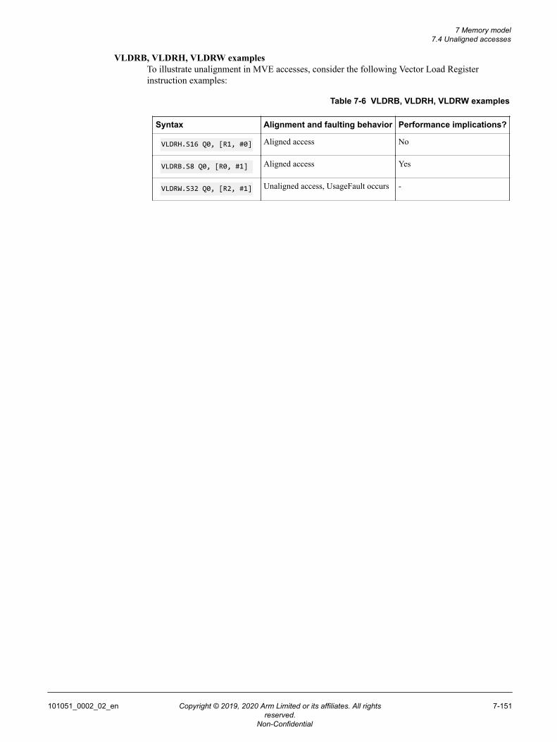
VLDRB, VLDRH, VLDRW examplesTo illustrate unalignment in MVE accesses, consider the following Vector Load Registerinstruction examples:
Table 7-6 VLDRB, VLDRH, VLDRW examples
Syntax Alignment and faulting behavior Performance implications?
VLDRH.S16 Q0, [R1, #0] Aligned access No
VLDRB.S8 Q0, [R0, #1] Aligned access Yes
VLDRW.S32 Q0, [R2, #1] Unaligned access, UsageFault occurs -
7 Memory model7.4 Unaligned accesses
101051_0002_02_en Copyright © 2019, 2020 Arm Limited or its affiliates. All rightsreserved.
7-151
Non-Confidential
7.5 Access privilege level for Device and Normal memoryThe AMBA 5 AXI, AMBA 5 AHB, and AMBA 4 APB protocols include signals that allow the privilegelevel of an access to be reported to the system.
The Cortex-M55 processor supports these signals across the Master AXI (M-AXI), Peripheral AHB (P-AHB), and External Private Peripheral Bus (EPPB) interfaces for Device memory. It also supportsprivilege reporting for Normal memory on P-AHB. However, accesses to Normal memory on M-AXIcan be buffered and cached so memory read and write requests and instruction fetches from bothprivileged and unprivileged software can be merged. For these transactions, the AXI signalsARPROT[0] and AWPROT[0] are always 1 indicating a privileged access. Access permission to aregion of memory can always be restricted to software running in privileged mode by using the MemoryProtection Unit (MPU).
The Instruction Tightly Coupled Memory (ITCM) and Data Tightly Coupled Memory (DTCM) interfacesprovide signals ITCMPRIV, D0TCMPRIV, D1TCMPRIV, D2TCMPRIV, and D3TCMPRIV toindicate the privilege of all memory accesses.
For more information on these signals, see the C.7 Instruction Tightly Coupled Memory interface signalson page Appx-C-384 and C.8 Data Tightly Coupled Memory interface signals on page Appx-C-386.
7 Memory model7.5 Access privilege level for Device and Normal memory
101051_0002_02_en Copyright © 2019, 2020 Arm Limited or its affiliates. All rightsreserved.
7-152
Non-Confidential
7.6 Memory ordering and barriersTransactions that are performed on different interfaces can be reordered relative to one another, even ifone or more of them is to Device memory.
In this context, the Internal Private Peripheral Bus (IPPB) region must be considered as a distinctinterface. Therefore, PPB accesses can be reordered relative to Device accesses performed on thePeripheral AHB (P-AHB) or Master AXI (M-AXI).
This is consistent with the architectural memory ordering requirements as defined in the Arm®v8-MArchitecture Reference Manual based on the assumption that the same peripheral is never mapped ontomultiple interfaces.
If stricter ordering is required between two transactions to different interfaces, a DMB or DSB instructionmust be inserted between them. For transactions to the same interface, two transactions to Devicememory are always performed in program order.
TCMs are always implicitly Normal memory and any attempt to enforce stricter requirements bychanging Memory Protection Unit (MPU) attributes are ignored.
The Armv8.1‑M architecture includes the load-acquire and store-release instructions. These can be usedto implement hardware-level support for the C++11 standard library atomic operations.
ISB instructions are required to guarantee the effect of instructions during context changes because theprocessor can prefetch several instructions before they are executed.
7 Memory model7.6 Memory ordering and barriers
101051_0002_02_en Copyright © 2019, 2020 Arm Limited or its affiliates. All rightsreserved.
7-153
Non-Confidential
7.7 Execute Only MemoryThe Cortex-M55 processor supports system level use of eXecute Only Memory (XOM) on the MasterAXI (M-AXI) and Tightly Coupled Memory (TCM) interfaces. The system integrator is responsible foradding relevant system design logic to support use of XOM.
In an XOM configuration, memory that is designated as execute-only cannot be read directly orindirectly by software running on the processor, or by the debugger. XOM operation requires thatsoftware is compiled so that literals are constructed through instruction fetches rather than explicit loadsfrom memory. For example, using the MOVT and MOVW instructions.
XOM on the TCM interfaces is supported by the xTCMMASTER output signal which is set to 0b0000for instruction fetches from software running on the processor. Any access to an XOM region which isnot recognized as an instruction fetch can be aborted by asserting the xTCMERR signal. XOM regionsprotected in this way can never be accessed by Slave AHB (S-AHB) as a read on the slave interface willalways result in a TCM access with xTCMMASTER set to 0b0011.
XOM on the AXI interface requires that instruction fetches can be identified on the AXI interface. Thiscan be done by checking the AXI read ID, ARPROT[2] which is only asserted for instruction fetchrequests. The processor supports direct access to the cache RAM, therefore, access to the L1 instructioncache must also be restricted. This can be achieved by asserting the external input signal LOCKDCAIC.
For more information on XOM, see the Arm®v8-M Architecture Reference Manual.
7 Memory model7.7 Execute Only Memory
101051_0002_02_en Copyright © 2019, 2020 Arm Limited or its affiliates. All rightsreserved.
7-154
Non-Confidential
Chapter 8Memory Authentication
This chapter describes the Memory Authentication Unit (MAU) responsible for controlling access tomemory.
It contains the following sections:• 8.1 MAU features on page 8-156.• 8.2 Security Attribution Unit on page 8-157.• 8.3 Memory Protection Unit on page 8-159.• 8.4 Implementation Defined Attribution Unit on page 8-161.• 8.5 Memory regions not controlled by SAU and IDAU on page 8-162.• 8.6 Security attribution signals on page 8-163.• 8.7 TCM Gate Units on page 8-164.• 8.8 TCM and P-AHB security access control on page 8-165.
101051_0002_02_en Copyright © 2019, 2020 Arm Limited or its affiliates. All rightsreserved.
8-155
Non-Confidential
8.1 MAU featuresThe Memory Authentication Unit (MAU) receives requests from units that perform memory accesses,and the MAU returns responses to these units. These responses are a combination of all the responsesfrom the Memory Protection Unit (MPU), Security Attribution Unit (SAU), Implementation DefinedAttribution Unit (IDAU), and TCM Gate Unit (TGU). The MAU contains the following units orinterfaces to units.
• MPU. For more information, see the 8.3 Memory Protection Unit on page 8-159.• TGU. For more information, see the 8.7 TCM Gate Units on page 8-164.• SAU. For more information, see the 8.2 Security Attribution Unit on page 8-157.• Interface to the IDAU. For more information, see the 8.4 Implementation Defined Attribution Unit
on page 8-161.• Interface to the Load Store Unit (LSU) from the MAU. The LSU makes MAU lookup requests for
loads, stores, and Preload Data (PLD), linefills, evictions, stacking, and unstacking.• Interface to the TCMs from the TGU. The TCMs make TGU requests through the Slave AHB (S-
AHB) interface for Direct Memory Accesses (DMAs), unstacking requests, instruction fetches, andloads and stores from the processor. For more information, see the 9.8 TCM interfaces on page 9-192.
• Interface to the Instruction Fetch Unit (IFU) from the MAU. The IFU makes lookup requests forinstructions and vector fetches.
Note
When changing security attribution of an address by either reprogramming the SAU or changing theexternal IDAU mappings, cache maintenance is required.
8 Memory Authentication8.1 MAU features
101051_0002_02_en Copyright © 2019, 2020 Arm Limited or its affiliates. All rightsreserved.
8-156
Non-Confidential
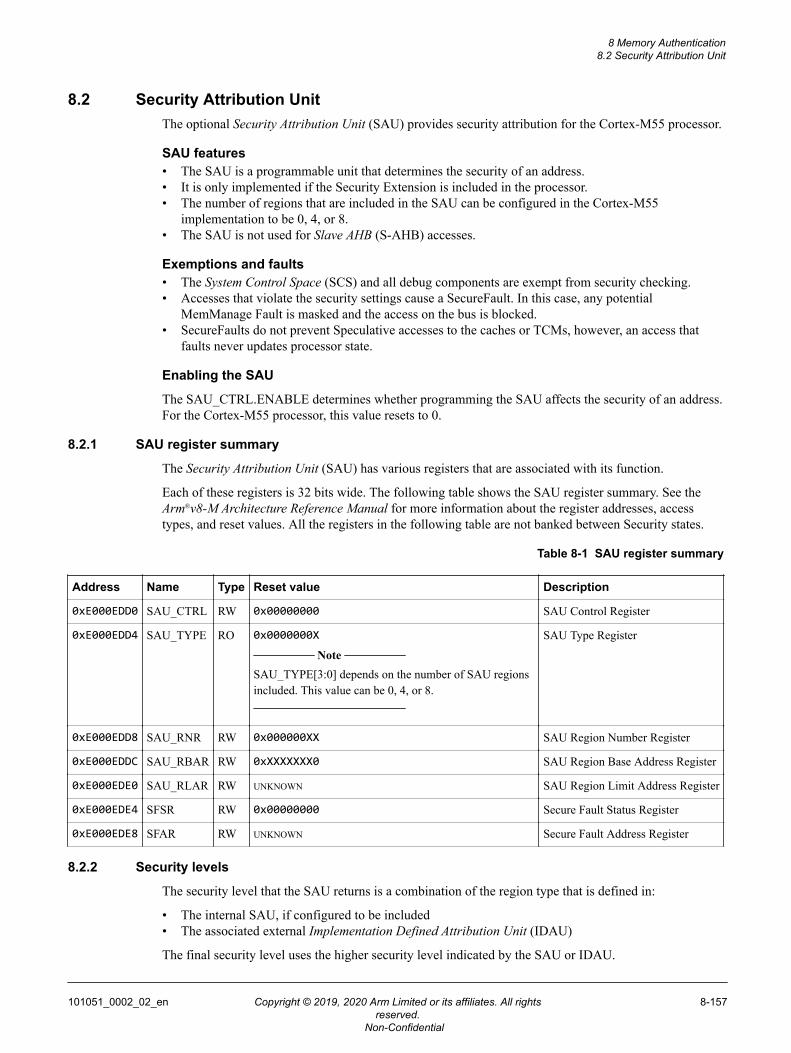
8.2 Security Attribution UnitThe optional Security Attribution Unit (SAU) provides security attribution for the Cortex-M55 processor.
SAU features• The SAU is a programmable unit that determines the security of an address.• It is only implemented if the Security Extension is included in the processor.• The number of regions that are included in the SAU can be configured in the Cortex-M55
implementation to be 0, 4, or 8.• The SAU is not used for Slave AHB (S-AHB) accesses.
Exemptions and faults• The System Control Space (SCS) and all debug components are exempt from security checking.• Accesses that violate the security settings cause a SecureFault. In this case, any potential
MemManage Fault is masked and the access on the bus is blocked.• SecureFaults do not prevent Speculative accesses to the caches or TCMs, however, an access that
faults never updates processor state.
Enabling the SAU
The SAU_CTRL.ENABLE determines whether programming the SAU affects the security of an address.For the Cortex-M55 processor, this value resets to 0.
8.2.1 SAU register summary
The Security Attribution Unit (SAU) has various registers that are associated with its function.
Each of these registers is 32 bits wide. The following table shows the SAU register summary. See theArm®v8-M Architecture Reference Manual for more information about the register addresses, accesstypes, and reset values. All the registers in the following table are not banked between Security states.
Table 8-1 SAU register summary
Address Name Type Reset value Description
0xE000EDD0 SAU_CTRL RW 0x00000000 SAU Control Register
0xE000EDD4 SAU_TYPE RO 0x0000000X Note
SAU_TYPE[3:0] depends on the number of SAU regionsincluded. This value can be 0, 4, or 8.
SAU Type Register
0xE000EDD8 SAU_RNR RW 0x000000XX SAU Region Number Register
0xE000EDDC SAU_RBAR RW 0xXXXXXXX0 SAU Region Base Address Register
0xE000EDE0 SAU_RLAR RW UNKNOWN SAU Region Limit Address Register
0xE000EDE4 SFSR RW 0x00000000 Secure Fault Status Register
0xE000EDE8 SFAR RW UNKNOWN Secure Fault Address Register
8.2.2 Security levels
The security level that the SAU returns is a combination of the region type that is defined in:
• The internal SAU, if configured to be included• The associated external Implementation Defined Attribution Unit (IDAU)
The final security level uses the higher security level indicated by the SAU or IDAU.
8 Memory Authentication8.2 Security Attribution Unit
101051_0002_02_en Copyright © 2019, 2020 Arm Limited or its affiliates. All rightsreserved.
8-157
Non-Confidential
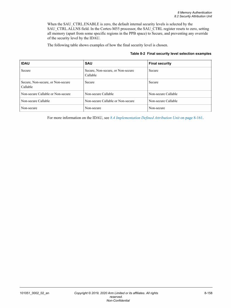
When the SAU_CTRL.ENABLE is zero, the default internal security levels is selected by theSAU_CTRL.ALLNS field. In the Cortex-M55 processor, the SAU_CTRL register resets to zero, settingall memory (apart from some specific regions in the PPB space) to Secure, and preventing any overrideof the security level by the IDAU.
The following table shows examples of how the final security level is chosen.
Table 8-2 Final security level selection examples
IDAU SAU Final security
Secure Secure, Non-secure, or Non-secureCallable
Secure
Secure, Non-secure, or Non-secureCallable
Secure Secure
Non-secure Callable or Non-secure Non-secure Callable Non-secure Callable
Non-secure Callable Non-secure Callable or Non-secure Non-secure Callable
Non-secure Non-secure Non-secure
For more information on the IDAU, see 8.4 Implementation Defined Attribution Unit on page 8-161.
8 Memory Authentication8.2 Security Attribution Unit
101051_0002_02_en Copyright © 2019, 2020 Arm Limited or its affiliates. All rightsreserved.
8-158
Non-Confidential
8.3 Memory Protection UnitThe Cortex-M55 processor supports Arm Protected Memory System Architecture (PMSA). The MemoryProtection Unit (MPU) is an optional component that is primarily used for memory region protection.
MPU featuresThe MPU features include:• Memory region protection.• Access permissions.• Exporting memory attributes to the system.• The MPU is not used for Slave AHB (S-AHB) accesses.• You can use the MPU to:
— Enforce privilege rules.— Separate processes.— Manage memory attributes.
Permission and access violations
MPU mismatches and permission violations invoke the MemManage Fault handler. These violationsresult in MemManage Faults and the access on the bus is blocked. For more information on MemManageFaults, see the Arm®v8-M Architecture Reference Manual. MemManage Faults do not preventSpeculative accesses to the caches or TCMs, however, an access that faults never updates processor state.
MPU configuration
The MPU can be configured to support 0, 4, 8, 12, or 16 memory regions.
If the Security Extension is included in the Cortex-M55 processor, memory protection can be duplicatedbetween Secure and Non-secure MPU (MPU_S and MPU_NS).
The number of regions in the Secure and Non-secure MPU can be configured independently, and eachcan be programmed to protect memory for the associated Security state.
8.3.1 Memory Protection Unit register summary
The Memory Protection Unit (MPU) has various registers that are associated with its function.
Each of these registers is 32 bits wide. If the MPU is not present in the implementation, then all of theseregisters Read-As-Zero (RAZ). The following table shows the MPU register summary.
Each of these registers is 32 bits wide. The following table shows the MPU register summary.
See the Arm®v8-M Architecture Reference Manual for more information about the register addresses,access types, and reset values. All the registers in the following table are banked between Security states.
Table 8-3 MPU register summary
Address Name Type Reset value Description
0xE000ED90 MPU_TYPE RO 0x0000xx00 Note
MPU_TYPE[15:8] depends on the number ofMPU regions configured. This value can be 0, 4,8, 12, or 16.
MPU Type Register
0xE000ED94 MPU_CTRL RW 0x00000000 MPU ControlRegister
8 Memory Authentication8.3 Memory Protection Unit
101051_0002_02_en Copyright © 2019, 2020 Arm Limited or its affiliates. All rightsreserved.
8-159
Non-Confidential
Table 8-3 MPU register summary (continued)
Address Name Type Reset value Description
0xE000ED98 MPU_RNR RW 0x000000XX MPU RegionNumber Register
0xE000ED9C MPU_RBAR RW UNKNOWN MPU Region BaseAddress Register
0xE000EDA0 MPU_RLAR RW UNKNOWN, bit [0] resets to 0. MPU Region LimitAddress Register
0xE000EDA4 MPU_RBAR_A1 RW UNKNOWN MPU Region BaseAddress RegisterAlias 1
0xE000EDA8 MPU_RLAR_A1 RW UNKNOWN MPU Region LimitAddress RegisterAlias 1
0xE000EDAC MPU_RBAR_A2 RW UNKNOWN MPU Region BaseAddress RegisterAlias 2
0xE000EDB0 MPU_RLAR_A2 RW UNKNOWN MPU Region LimitAddress RegisterAlias 2
0xE000EDB4 MPU_RBAR_A3 RW UNKNOWN MPU Region BaseAddress RegisterAlias 3
0xE000EDB8 MPU_RLAR_A3 RW UNKNOWN MPU Region LimitAddress RegisterAlias 3
0xE000EDC0 MPU_MAIR0 RW UNKNOWN MPU MemoryAttribute IndirectionRegister 0
0xE000EDC4 MPU_MAIR1 RW UNKNOWN MPU MemoryAttribute IndirectionRegister 1
8 Memory Authentication8.3 Memory Protection Unit
101051_0002_02_en Copyright © 2019, 2020 Arm Limited or its affiliates. All rightsreserved.
8-160
Non-Confidential
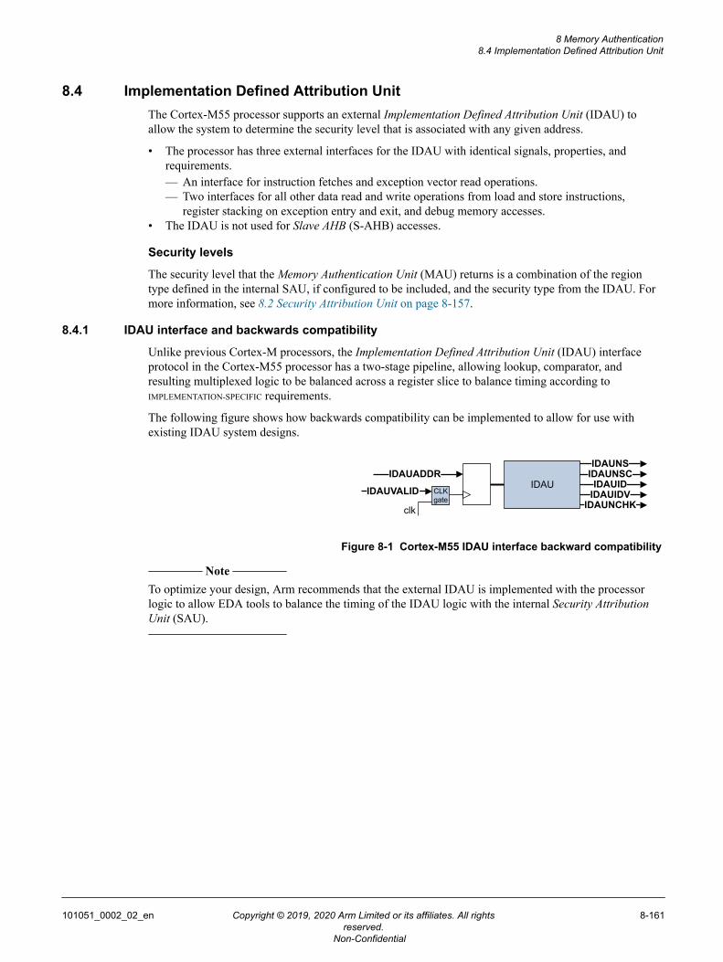
8.4 Implementation Defined Attribution UnitThe Cortex-M55 processor supports an external Implementation Defined Attribution Unit (IDAU) toallow the system to determine the security level that is associated with any given address.
• The processor has three external interfaces for the IDAU with identical signals, properties, andrequirements.— An interface for instruction fetches and exception vector read operations.— Two interfaces for all other data read and write operations from load and store instructions,
register stacking on exception entry and exit, and debug memory accesses.• The IDAU is not used for Slave AHB (S-AHB) accesses.
Security levels
The security level that the Memory Authentication Unit (MAU) returns is a combination of the regiontype defined in the internal SAU, if configured to be included, and the security type from the IDAU. Formore information, see 8.2 Security Attribution Unit on page 8-157.
8.4.1 IDAU interface and backwards compatibility
Unlike previous Cortex‑M processors, the Implementation Defined Attribution Unit (IDAU) interfaceprotocol in the Cortex-M55 processor has a two-stage pipeline, allowing lookup, comparator, andresulting multiplexed logic to be balanced across a register slice to balance timing according toIMPLEMENTATION-SPECIFIC requirements.
The following figure shows how backwards compatibility can be implemented to allow for use withexisting IDAU system designs.
IDAUIDAUADDR
IDAUNSIDAUNSCIDAUID
IDAUIDVIDAUNCHK
CLK gate
IDAUVALID
clk
Figure 8-1 Cortex-M55 IDAU interface backward compatibility
Note
To optimize your design, Arm recommends that the external IDAU is implemented with the processorlogic to allow EDA tools to balance the timing of the IDAU logic with the internal Security AttributionUnit (SAU).
8 Memory Authentication8.4 Implementation Defined Attribution Unit
101051_0002_02_en Copyright © 2019, 2020 Arm Limited or its affiliates. All rightsreserved.
8-161
Non-Confidential
8.5 Memory regions not controlled by SAU and IDAUThe entire IPPB and EPPB region of the memory map is not controlled by the Security Attribution Unit(SAU) and Implementation Defined Attribution Unit (IDAU). Additionally, IMPLEMENTATION-DEFINED
registers (0xE001E000-0xE001FFFF) and IMPLEMENTATION-DEFINED Non-secure alias registers(0xE003E000-0xE003FFFF) are not controlled by the SAU and IDAU. These regions are only controlledby the Security state of the processor.
For more information on these regions, see 7.3 Private Peripheral Bus on page 7-148.
8 Memory Authentication8.5 Memory regions not controlled by SAU and IDAU
101051_0002_02_en Copyright © 2019, 2020 Arm Limited or its affiliates. All rightsreserved.
8-162
Non-Confidential
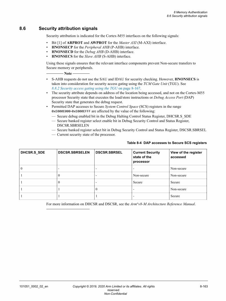
8.6 Security attribution signalsSecurity attribution is indicated for the Cortex-M55 interfaces on the following signals:
• Bit [1] of ARPROT and AWPROT for the Master AXI (M-AXI) interface.• HNONSECP for the Peripheral AHB (P-AHB) interface.• HNONSECD for the Debug AHB (D-AHB) interface.• HNONSECS for the Slave AHB (S-AHB) interface.
Using these signals ensures that the relevant interface components prevent Non-secure transfers toSecure memory or peripherals.
Note
• S-AHB requests do not use the SAU and IDAU for security checking. However, HNONSECS istaken into consideration for security access gating using the TCM Gate Unit (TGU). See8.8.2 Security access gating using the TGU on page 8-167.
• The security attribute depends on address of the location being accessed, and not on the Cortex-M55processor Security state that executes the load/store instructions or Debug Access Port (DAP)Security state that generates the debug request.
• Permitted DAP accesses to Secure System Control Space (SCS) registers in the range0xE000E000-0xE000EFFF are affected by the value of the following:— Secure debug enabled bit in the Debug Halting Control Status Register, DHCSR.S_SDE— Secure banked register select enable bit in Debug Security Control and Status Register,
DSCSR.SBRSELEN— Secure banked register select bit in Debug Security Control and Status Register, DSCSR.SBRSEL— Current security state of the processor.
Table 8-4 DAP accesses to Secure SCS registers
DHCSR.S_SDE DSCSR.SBRSELEN DSCSR.SBRSEL Current Securitystate of theprocessor
View of the registeraccessed
0 - - - Non-secure
1 0 - Non-secure Non-secure
1 0 - Secure Secure
1 1 0 - Non-secure
1 1 1 - Secure
For more information on DHCSR and DSCSR, see the Arm®v8-M Architecture Reference Manual.
8 Memory Authentication8.6 Security attribution signals
101051_0002_02_en Copyright © 2019, 2020 Arm Limited or its affiliates. All rightsreserved.
8-163
Non-Confidential
8.7 TCM Gate UnitsThere are two TCM Gate Units (TGUs), one for Instruction Tightly Coupled Memory (ITCM) accesses(ITGU), and one for Data Tightly Coupled Memory (DTCM) accesses (DTGU), that are responsible forTCM security gating and control.
For more information on how the TGUs are responsible for security access control, see 8.8 TCM and P-AHB security access control on page 8-165.
8 Memory Authentication8.7 TCM Gate Units
101051_0002_02_en Copyright © 2019, 2020 Arm Limited or its affiliates. All rightsreserved.
8-164
Non-Confidential
8.8 TCM and P-AHB security access controlThe Cortex-M55 processor provides a mechanism to support further or a more fine-grained securityaccess control on the TCM and Peripheral AHB (P-AHB) interfaces than provided by the SAU andIDAU.
This mechanism is compatible with the external gating mechanism described in Arm® Platform SecurityArchitecture Trusted Base System Architecture for Arm®v6‑M, Arm®v7‑M, and Arm®v8‑M.
To achieve additional security access control, you must use memory aliasing, configure theImplementation Defined Attribution Unit (IDAU) or Security Attribution Unit (SAU), and implementsecurity gating.
Memory aliasing and IDAU and SAU configurationMemory aliasing can be applied to the TCM and P-AHB interfaces. Memory aliasing is aduplication of all memory-mapped components in Secure and Non-secure address regions.These regions must be defined as Secure and Non-secure using the IDAU or SAU. For moreinformation, see 8.8.1 Memory aliasing and IDAU/SAU configuration on page 8-165.
For more information on the SAU and IDAU, see 8.2 Security Attribution Unit on page 8-157and 8.4 Implementation Defined Attribution Unit on page 8-161 respectively.
Security gatingThe TCM Gate Unit (TGU) provides security gating for TCM accesses only. For moreinformation on TGU security gating, see 8.8.2 Security access gating using the TGUon page 8-167.
To implement memory aliasing with the TCMs, you must use the TGU to maximize the benefitsof the additional level of security that it provides.
If memory aliasing is not enabled (using the CFGMEMALIAS signal), the TGU is not used.
Accesses to the P-AHB require you to include your own external security gating logic.
Note
Additionally, memory aliasing can be done for the AXI interface, and all gating must be implementedexternally. Therefore, the description of this behavior is outside the scope of this document. For moreinformation, see the Arm® Platform Security Architecture Trusted Base System Architecture forArm®v6‑M, Arm®v7‑M, and Arm®v8‑M.
8.8.1 Memory aliasing and IDAU/SAU configuration
In normal operation, the TCM and Peripheral AHB (P-AHB) interfaces are mapped to regions in thememory map.
Code region Base address 0x00000000 is used for Instruction Tightly Couple Memory (ITCM).SRAM region Base address 0x20000000 is used for Data Tightly Couple Memory (DTCM).Peripheral region Base address 0x40000000 is used for P-AHB.
The TCM regions extend from their base to a limit that is defined by the physical size (in bytes) of theTCM set by the input signals CFGITCMSZ and CFGDTCMSZ. The P-AHB region extends from thebase to its region size (in bytes) defined by the CFGPAHBSZ input signal.
Memory aliasing is enabled by tying the external input signal CFGMEMALIAS[4:0] to a non-zerovalue. The aliased address bit can be set from bit [24] to bit [28] using the CFGMEMALIAS[4:0]signal. The address bit that is used for memory alias is determined by the following options:
• 0b00001, indicating that the alias bit is bit[24].• 0b00010, indicating that the alias bit is bit[25].• 0b00100, indicating that the alias bit is bit[26].
8 Memory Authentication8.8 TCM and P-AHB security access control
101051_0002_02_en Copyright © 2019, 2020 Arm Limited or its affiliates. All rightsreserved.
8-165
Non-Confidential
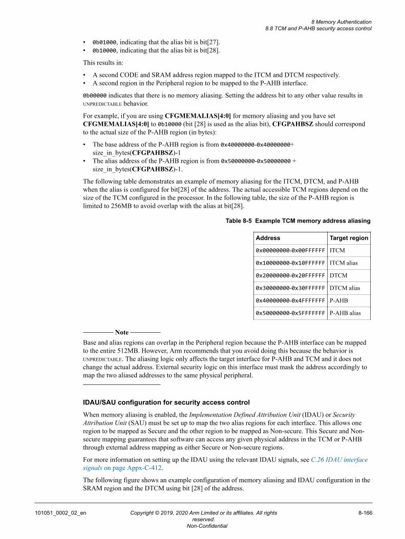
• 0b01000, indicating that the alias bit is bit[27].• 0b10000, indicating that the alias bit is bit[28].
This results in:
• A second CODE and SRAM address region mapped to the ITCM and DTCM respectively.• A second region in the Peripheral region to be mapped to the P-AHB interface.
0b00000 indicates that there is no memory aliasing. Setting the address bit to any other value results inUNPREDICTABLE behavior.
For example, if you are using CFGMEMALIAS[4:0] for memory aliasing and you have setCFGMEMALIAS[4:0] to 0b10000 (bit [28] is used as the alias bit), CFGPAHBSZ should correspondto the actual size of the P-AHB region (in bytes):
• The base address of the P-AHB region is from 0x40000000-0x40000000+size_in_bytes(CFGPAHBSZ)-1
• The alias address of the P-AHB region is from 0x50000000-0x50000000 +size_in_bytes(CFGPAHBSZ)-1.
The following table demonstrates an example of memory aliasing for the ITCM, DTCM, and P-AHBwhen the alias is configured for bit[28] of the address. The actual accessible TCM regions depend on thesize of the TCM configured in the processor. In the following table, the size of the P-AHB region islimited to 256MB to avoid overlap with the alias at bit[28].
Table 8-5 Example TCM memory address aliasing
Address Target region
0x00000000-0x00FFFFFF ITCM
0x10000000-0x10FFFFFF ITCM alias
0x20000000-0x20FFFFFF DTCM
0x30000000-0x30FFFFFF DTCM alias
0x40000000-0x4FFFFFFF P-AHB
0x50000000-0x5FFFFFFF P-AHB alias
Note
Base and alias regions can overlap in the Peripheral region because the P-AHB interface can be mappedto the entire 512MB. However, Arm recommends that you avoid doing this because the behavior isUNPREDICTABLE. The aliasing logic only affects the target interface for P-AHB and TCM and it does notchange the actual address. External security logic on this interface must mask the address accordingly tomap the two aliased addresses to the same physical peripheral.
IDAU/SAU configuration for security access control
When memory aliasing is enabled, the Implementation Defined Attribution Unit (IDAU) or SecurityAttribution Unit (SAU) must be set up to map the two alias regions for each interface. This allows oneregion to be mapped as Secure and the other region to be mapped as Non-secure. This Secure and Non-secure mapping guarantees that software can access any given physical address in the TCM or P-AHBthrough external address mapping as either Secure or Non-secure regions.
For more information on setting up the IDAU using the relevant IDAU signals, see C.26 IDAU interfacesignals on page Appx-C-412.
The following figure shows an example configuration of memory aliasing and IDAU configuration in theSRAM region and the DTCM using bit [28] of the address.
8 Memory Authentication8.8 TCM and P-AHB security access control
101051_0002_02_en Copyright © 2019, 2020 Arm Limited or its affiliates. All rightsreserved.
8-166
Non-Confidential
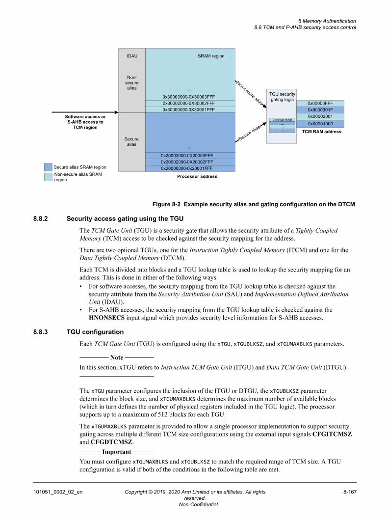
...
...
0x30003000-0X30003FFF0x30002000-0X30002FFF0x30000000-0X30001FFF
0x20003000-0X20003FFF0x20002000-0X20002FFF0x20000000-0x20001FFF
Secure alias
Non-secure alias
IDAU SRAM region
TGU security gating logic
Non-secure alias
Secure alias
Processor address
TCM RAM address
0x00002001
0x00003FFF0x0000301F
0x00001000...
Lookup table...
...
Software access or S-AHB access to
TCM region
Secure alias SRAM regionNon-secure alias SRAM region
Figure 8-2 Example security alias and gating configuration on the DTCM
8.8.2 Security access gating using the TGU
The TCM Gate Unit (TGU) is a security gate that allows the security attribute of a Tightly CoupledMemory (TCM) access to be checked against the security mapping for the address.
There are two optional TGUs, one for the Instruction Tightly Coupled Memory (ITCM) and one for theData Tightly Coupled Memory (DTCM).
Each TCM is divided into blocks and a TGU lookup table is used to lookup the security mapping for anaddress. This is done in either of the following ways:• For software accesses, the security mapping from the TGU lookup table is checked against the
security attribute from the Security Attribution Unit (SAU) and Implementation Defined AttributionUnit (IDAU).
• For S-AHB accesses, the security mapping from the TGU lookup table is checked against theHNONSECS input signal which provides security level information for S-AHB accesses.
8.8.3 TGU configuration
Each TCM Gate Unit (TGU) is configured using the xTGU, xTGUBLKSZ, and xTGUMAXBLKS parameters.
Note
In this section, xTGU refers to Instruction TCM Gate Unit (ITGU) and Data TCM Gate Unit (DTGU).
The xTGU parameter configures the inclusion of the ITGU or DTGU, the xTGUBLKSZ parameterdetermines the block size, and xTGUMAXBLKS determines the maximum number of available blocks(which in turn defines the number of physical registers included in the TGU logic). The processorsupports up to a maximum of 512 blocks for each TGU.
The xTGUMAXBLKS parameter is provided to allow a single processor implementation to support securitygating across multiple different TCM size configurations using the external input signals CFGITCMSZand CFGDTCMSZ.
Important
You must configure xTGUMAXBLKS and xTGUBLKSZ to match the required range of TCM size. A TGUconfiguration is valid if both of the conditions in the following table are met.
8 Memory Authentication8.8 TCM and P-AHB security access control
101051_0002_02_en Copyright © 2019, 2020 Arm Limited or its affiliates. All rightsreserved.
8-167
Non-Confidential
Table 8-6 TGU configuration conditional validity
Condition Formula
Block size * Maximum number of blocks = Maximum physicalsize of the TCM
xTGUBLKSZ + xTGUMAXBLKS = CFGxTCMSZmax + 4.
Block size < Minimum physical size of the TCM xTGUBLKSZ < CFGxTCMSZmin + 4
This ensures that there are enough blocks to cover the largest TCM size and that at least two blocks coverthe minimum TCM size. If these parameters are configured incorrectly, the TGU behavior becomesUNPREDICTABLE.
For a given processor implementation and integration, reading the xTGU_CFG.NUMBLKS andxTGU_CFG.BLKSZ register bitfields determines the number of available blocks in the lookup table andthe block size respectively. For more information on these registers, see 4.20.2 ITGU_CFG andDTGU_CFG, ITGU and DTGU Configuration Registers on page 4-104 .
When TCM gating is enabled, the Code and SRAM region of the processor memory map is aliased sothat two regions map onto the same physical TCM address. These two regions should be mapped todifferent security levels. The security level attributed to the logical address used by software is alwaysused to control the TGU. The two alias regions always map to the same physical address in the TCMmemory.
The following table shows an example configuration where the processor ITGU is configured with 1KBblocks and supports a maximum ITCM size of 64KB and a minimum ITCM size of 4KB. In this case,ITGUMAXBLKS must be configured to 0b0110 or 64 blocks.
Table 8-7 Example TGU configuration for 1KB block size
ITCM size CFGITCMSZ ITGUBLKSZ ITGUMAXBLKS ITGU_CFG.NUMBLKS ITGU_CFG.BLKSZ
4KB 0b0011 0b0101 0b0110 0b0010 0b0101
8KB 0b0100 0b0101 0b0110 0b0011 0b0101
16KB 0b0101 0b0101 0b0110 0b0100 0b0101
32KB 0b0110 0b0101 0b0110 0b0101 0b0101
64KB 0b0111 0b0101 0b0110 0b0110 0b0101
TGU block lookup table
Each block entry in the lookup table can be accessed by software using the xTGU_LUTn registers. Eachregister contains up to 32 block entries. For a valid block, the entry bit determines the required securitylevel. All blocks reset to 0, therefore, at reset, all TCM memory is considered as Secure.
Any unused block entries in the lookup table, due to the configuration, do not affect the operation of thesecurity gate and the corresponding xTGU_LUTn bitfield is RAZ/WI when accessed by software.
TGU enable and locking
TCM gating is enabled by tying the external input signal CFGMEMALIAS to a non-zero value.
The TGU can be locked from software access using the external input signals LOCKITGU andLOCKDTGU. When these signals are asserted the corresponding TGU registers become read-only. Thisallows a TGU configuration to be programmed and then locked from further changes by software.
8 Memory Authentication8.8 TCM and P-AHB security access control
101051_0002_02_en Copyright © 2019, 2020 Arm Limited or its affiliates. All rightsreserved.
8-168
Non-Confidential
8.8.4 Security check and fault response
Accesses to a memory region that the TGU protects only proceed if the security level of the requestmatches the programmed security of the block. At reset, all blocks are Secure.
• Read requests on the external TCM interfaces are always Speculative, regardless of whether theaccess passes the security check in the TGU. Data from the RAM is always ignored if the check failsand the processor state is never updated.
• If the security check fails, write requests are always ignored and never carried out on the TCMinterface.
The result of a security check mismatch in the TGU depends on the type of the access and theconfiguration of the ITGU_CTRL or DTGU_CTRL registers. The access is either ignored or generates afault:• A security check mismatch on an instruction fetch always results in a BusFault. The fault is recorded
in AFSR.FTGU.• If ITGU_CTRL.DBFEN or DTGU_CTRL.DBFEN is set, a security check mismatch on a data read
or write results in a precise BusFault. The fault is recorded in AFSR.PTGU. If ITGU_CTRL.DBFENor DTGU_CTRL.DBFEN is not set, no exception is raised.
• If ITGU_CTRL.DBGEN or DTGU_CTRL.DBEN is set, then a security check mismatch on a debugrequest causes HRESP to be asserted on the Debug AHB (D-AHB) interface. AFSR.PTGU is notupdated on a security check mismatch from a debug request.
• If ITGU_CTRL.DEREN or DTGU_CTRL.DEREN is set, a security check mismatch on a read orwrite to the TCM from the S-AHB signals an error on the interface. For all mismatched readaccesses, zero is returned to prevent any leaks of Secure data.
Note
If a data read access on the TCM returns an error on the interface (ITCMERR or DTCMERR inputsignal is asserted) for an address which fails the TGU security check and ITGU_CTRL.DBFEN orDTGU_CTRL.DBFEN is not set, then the overall behavior is RAZ/WI instead of raising a BusFault.This is consistent with a security fault response from the Memory Authentication Unit (MAU).
8 Memory Authentication8.8 TCM and P-AHB security access control
101051_0002_02_en Copyright © 2019, 2020 Arm Limited or its affiliates. All rightsreserved.
8-169
Non-Confidential
Chapter 9Memory system
This chapter describes the Cortex-M55 processor memory system.
It contains the following sections:• 9.1 Memory system features on page 9-171.• 9.2 Memory system faults on page 9-173.• 9.3 Memory system behavior on page 9-175.• 9.4 Master-AXI interface on page 9-179.• 9.5 Peripheral AHB interface on page 9-185.• 9.6 S-AHB interface on page 9-188.• 9.7 EPPB interface on page 9-191.• 9.8 TCM interfaces on page 9-192.• 9.9 Instruction and data cache on page 9-196.• 9.10 Store buffer on page 9-204.• 9.11 Internal local exclusive access monitor on page 9-206.• 9.12 M-AXI and P-AHB interaction with the global exclusive monitor on page 9-207.• 9.13 MBIST on page 9-208.
101051_0002_02_en Copyright © 2019, 2020 Arm Limited or its affiliates. All rightsreserved.
9-170
Non-Confidential
9.1 Memory system featuresThe Cortex-M55 processor memory system is an interface between the processor core and the cacheRAMs, external memory interfaces and memory-mapped registers.
Note
For more information on how these units and interfaces interact with each other, see the Figure 2-1 Cortex-M55 processor block diagram on page 2-27.
Load Store UnitThe Load Store Unit (LSU) receives load and store accesses from the Data Processing Unit(DPU) and distributes these requests to the correct unit and returns any data or responses to theDPU. The LSU contains the Peripheral Interface Unit (PIU) which handles all the loads andstores to internal and external peripherals.
Peripheral Interface UnitThe Peripheral Interface Unit (PIU) is responsible for the handling of stores to peripheral unitsEPPB, IPPB, and P-AHB. The PIU coordinates the following accesses to the peripheral busses.• Loads from the LSU• Stores from the STB
TCM Control UnitThe TCM Control Unit (TCU) arbitrates requests between the LSU and Instruction Fetch Unit(IFU), accesses the TCMs, and returns any data or responses to the requesting unit. The TCUcontains a write queue for Slave-AHB (S-AHB) writes and a read prefetcher to improve theperformance of 32-bit and 64-bit incrementing reads.The TCU contains a small buffer for software stores to the TCM.
Tightly Coupled MemoriesThe Cortex-M55 processor has two TCM memory types, the Instruction Tightly CoupledMemory (ITCM) and Data Tightly Coupled Memory (DTCM). There is one ITCM interface andfour DTCM interfaces (D0TCM, D1TCM, D2TCM, and D3TCM respectively).All the TCM interfaces are 39 bits wide (32 bits for data and 7 bits for Error Correcting Code(ECC)).ECC generation and correction logic can optionally be included for each TCM interface and anECC error indication interface.
Memory accesses to the TCM, required for fetching instructions and for data transferinstructions, are performed if the address is in an enabled TCM region. Accesses that are notserviced by the TCM region are passed through the Master-AXI (M-AXI) interface or one of theperipheral interfaces.
Data Cache UnitThe Data Cache Unit (DCU) contains a four-way set-associative data cache and handles allaccesses to this cache. These accesses include loads, stores, cache maintenance operations,evictions, and ECC error detection and correction.The DCU can be configured to include logic to detect and process ECC errors.
Instruction Cache UnitThe Instruction Cache Unit (ICU) contains a two-way set-associative instruction cache, and itaccepts instruction fetch requests from the IFU and returns data from either the instructioncache, the linefill buffer, or the BIU.The ICU can be configured to include logic to detect and process ECC errors.
9 Memory system9.1 Memory system features
101051_0002_02_en Copyright © 2019, 2020 Arm Limited or its affiliates. All rightsreserved.
9-171
Non-Confidential
Store BufferThe Store Buffer (STB) has five 64-bit slots that buffer stores to the AXI bus.• For Cacheable stores, the STB sends a lookup request to the DCU to see if the target address
is in the cache. If it is, then the data is written directly to the cache. If the target address isnot in the cache and the access has a Write-Allocate hint, then the DCU makes a linefillrequest to the Bus Interface Unit (BIU) and writes the data into the BIU linefill buffer. If thetarget address is not in the cache and it does not have a Write-Allocate hint, then the store iswritten out to the AXI bus.
• For Non-cacheable data, the data is written to the BIU write buffer.• Write-Through stores are written out to the AXI bus even if they have been written into the
cache.
Bus Interface UnitThe BIU contains one 32-byte write buffer and two 32-byte linefill buffers.The BIU coordinates the following accesses to the M-AXI interface.• Loads from the LSU.• Stores from the STB.• Evictions from the DCU.• Fetches from the IFU.• Linefills triggered by PLD instructions.• Speculative linefills triggered by the data prefetcher.
Non-cacheable loads go directly to the AXI bus. Stores are buffered internally with the intentionof being combined in a burst on the AXI. Cacheable Read-Allocate loads and Cacheable Write-Allocate stores trigger linefills and the data from the AXI bus is buffered in the linefill bufferuntil the line is complete and it can be allocated in the DCU.
The linefill buffers also buffer load data from Non-cacheable bursts.
MBIST Interface UnitThe MBIST Interface Unit (MIU) provides the Memory Built-In Self Test (MBIST) interface.The MBIST interface supports production MBIST.
M-AXI interfaceThe M-AXI interface is 64 bits wide and connects to the external memory system.
Peripheral-AHB interfaceThe PIU includes a 32-bit Peripheral-AHB (P-AHB) interface for accessing externalperipherals.
Slave-AHB interfaceThe S-AHB interface is 64 bits wide and allows system accesses in and out of the TCMs.
PPB interfacesThe PIU includes the Internal Private Peripheral Bus (IPPB) interface to access internal PPBregisters, and the External PPB (EPPB) APB interface to access external PPB registers.
9 Memory system9.1 Memory system features
101051_0002_02_en Copyright © 2019, 2020 Arm Limited or its affiliates. All rightsreserved.
9-172
Non-Confidential
9.2 Memory system faultsMemory system faults can occur on instruction fetches and data accesses.
Faults can occur on instruction fetches for the following reasons:
• Memory Protection Unit (MPU) MemManage fault.• Security Attribution Unit (SAU) or Implementation Defined Attribution Unit (IDAU) SecureFault.• BusFaults that are caused by an external AXI slave error (SLVERR), an external AXI decode error
(DECERR), or corrupted transactions (RPOISON).• TCM external error.• Uncorrectable Error Correcting Code (ECC) errors in the TCM.• Breakpoints and vector catch events.• TCM Gate Unit (TGU) faults.
Faults can occur on data accesses for the following reasons:• MPU MemManage fault.• Alignment UsageFault.• SAU or IDAU SecureFault.• BusFaults that are caused by an external AXI slave error (SLVERR), an external AXI decode error
(DECERR), or corrupted read data (RPOISON).• BusFaults because of errors on the External Private Peripheral Bus (EPPB) APB interface.• External AHB error from the Peripheral-AHB (P-AHB) interface.• TCM external error.• Uncorrectable ECC errors in the TCM or L1 data cache.• Watchpoints.• M‑profile Vector Extension (MVE) transactions, stacking, or unstacking to the PPB space.• TGU faults.• Unprivileged accesses to system registers which only privileged code can access.
9.2.1 Classes of fault
Faults can be classified as MemManage Faults, BusFaults, SecureFaults, and UsageFaults.
MemManage faults
The Memory Protection Unit (MPU) can generate a fault for various reasons.
For more information on MemManage Faults, see Permission and access violations on page 8-159 .
Bus faults
A memory access or instruction fetch performed through the Master-AXI (M-AXI) interface can generatedifferent types of responses:
• Slave error (SLVERR).• Decode error (DECERR).
AXI bus errors cause precise or imprecise BusFaults. Additionally, if the AMBA 5 AXI signal,RPOISON, is asserted, an AXI read can generate a BusFault.
A memory access performed through the Peripheral AHB (P-AHB) interface can generate a single errorresponse. The processor manages this in the same way as a response of SLVERR from the AXI interface.
Whether a memory or instruction fetch access on the TCM interface can be performed or not relies onthe TCM Gate Unit (TGU), if implemented. Depending on the programming of the TGU, TGU faults cangenerate errors.
• For loads or stores, errors cause synchronous BusFaults.• For read and write accesses from the Slave AHB (S-AHB) interface, an error causes an AHB slave
error response on HRESPS. For writes, only TCM interface errors on ITCMERR or DTCMERRresult in an imprecise error response on S-AHB through SAHBWABORT.
9 Memory system9.2 Memory system faults
101051_0002_02_en Copyright © 2019, 2020 Arm Limited or its affiliates. All rightsreserved.
9-173
Non-Confidential
Synchronous BusFaults are generated in the following cases
• Instruction fetches.• Data loads.• Stores that generate a TGU fault.• Stores to PPB that cause a privilege violation.• M‑profile Vector Extension (MVE) stores and stacking to the PPB space.• Uncorrectable Error Correcting Code (ECC) errors.
Asynchronous BusFaults are generated in the following cases:• All stores except those that generate synchronous BusFaults.• Dirty linefills that cause an AXI bus error.• Unprivileged access to registers that can be accessed by privileged code only.
SecureFaults
If accesses do not pass the security attribution checks that the Memory Authentication Unit (MAU)performs, then a SecureFault is raised.
For more information on security attribution, see Memory Authentication Unit on page 2-30.
Note
In most of the memory regions, debugger accesses are subject to validation and attribution. That is, thefinal Security state of an access on the Master AXI (M-AXI), indicated on ARPROT[1] andAWPROT[1] signals, the Peripheral AHB (P-AHB) interface, indicated on HNONSECP signal, or theExternal Private Peripheral Bus (EPPB) APB interface, indicated on PPROT[1] signal, is set by theSecurity Attribution Unit (SAU) in the same way as software generated accesses. The SAU blocksmemory accesses which do not have the required permissions. For example, accesses to memory markedas Secure in the SAU when DHCSR.S_SDE is 0 or HNONSECD is HIGH. This results in an errorresponse on the Debug AHB (D-AHB) interface, but unlike accesses that originate from software, aSecureFault is not raised.
Usage faults
UsageFault exceptions occur in the following cases:
• Any unaligned access when CCR.UNALIGN_TRP is set results in an UNALIGNED UsageFaultexception. For more information on CCR, see the Arm®v8-M Architecture Reference Manual.
• Unaligned accesses to Device memory regions are not supported and result in an UNALIGNEDUsageFault exception.
• Unaligned accesses from an instruction that does not support unaligned accesses result in anUNALIGNED UsageFault exception. For more information on these instructions, see the Alignmentbehavior section in the Arm®v8-M Architecture Reference Manual
• For M‑profile Vector Extension (MVE) operations, a load or store access is considered unaligned ifthe address is not aligned to the specified element size. Using an address for an MVE load or storewhich is not aligned to the element size results in an UNALIGNED UsageFault being raised. Formore information on MVE and elements, see the Arm®v8-M Architecture Reference Manual.
• Accessing a coprocessor that does not exist results in a NOCP UsageFault.
Note
For more information on external coprocessors, see Chapter 12 External coprocessors on page 12-237.Additionally, for more usage restriction information, see 12.4 Coprocessor instruction restrictionson page 12-241.
9 Memory system9.2 Memory system faults
101051_0002_02_en Copyright © 2019, 2020 Arm Limited or its affiliates. All rightsreserved.
9-174
Non-Confidential
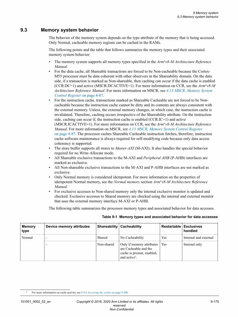
9.3 Memory system behaviorThe behavior of the memory system depends on the type attribute of the memory that is being accessed.Only Normal, cacheable memory regions can be cached in the RAMs.
The following points and the table that follows summarize the memory types and their associatedmemory system behavior:
• The memory system supports all memory types specified in the Arm®v8-M Architecture ReferenceManual.
• For the data cache, all Shareable transactions are forced to be Non-cacheable because the Cortex-M55 processor must be data coherent with other observers in the Shareability domain. On the dataside, if a transaction is marked as Non-shareable, then caching can occur if the data cache is enabled(CCR.DC=1) and active (MSCR.DCACTIVE=1). For more information on CCR, see the Arm®v8-MArchitecture Reference Manual. For more information on MSCR, see 4.13 MSCR, Memory SystemControl Register on page 4-87.
• For the instruction cache, transactions marked as Shareable Cacheable are not forced to be Non-cacheable because the instruction cache cannot be dirty and its contents are always consistent withthe external memory. Unless, the external memory changes, in which case, the instruction cache isinvalidated. Therefore, caching occurs irrespective of the Shareability attribute. On the instructionside, caching can occur if, the instruction cache is enabled (CCR.IC=1) and active(MSCR.ICACTIVE=1). For more information on CCR, see the Arm®v8-M Architecture ReferenceManual. For more information on MSCR, see 4.13 MSCR, Memory System Control Registeron page 4-87. The processor caches Shareable Cacheable instruction fetches, therefore, instructioncache software maintenance is always required for self-modifying code because only data accesscoherency is supported.
• The store buffer supports all stores to Master-AXI (M-AXI). It also handles the special behaviorrequired for no Write-Allocate mode.
• All Shareable exclusive transactions to the M-AXI and Peripheral AHB (P-AHB) interfaces aremarked as exclusive.
• All Non-shareable exclusive transactions to the M-AXI and P-AHB interfaces are not marked asexclusive.
• Only Normal memory is considered idempotent. For more information on the properties ofidempotent Normal memory, see the Normal memory section Arm®v8-M Architecture ReferenceManual.
• For exclusive accesses to Non-shared memory only the internal exclusive monitor is updated andchecked. Exclusive accesses to Shared memory are checked using the internal and external monitorthat uses the external memory interface M-AXI or P-AHB.
The following table summarizes the processor memory types and associated behavior for data accesses.
Table 9-1 Memory types and associated behavior for data accesses
Memorytype
Device memory attributes Shareability Cacheability Restartable Exclusiveshandled
Normal - Shared No Cacheability Yes Internal and external
- Non-shared Only if memory attributesare Cacheable and thecache is present, enabled,and activec.
Yes Internal only
c For more information on cache activity, see 9.9.6 Accessing the caches on page 9-200
9 Memory system9.3 Memory system behavior
101051_0002_02_en Copyright © 2019, 2020 Arm Limited or its affiliates. All rightsreserved.
9-175
Non-Confidential
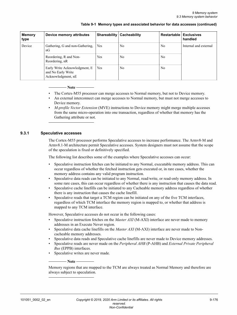
Table 9-1 Memory types and associated behavior for data accesses (continued)
Memorytype
Device memory attributes Shareability Cacheability Restartable Exclusiveshandled
Device Gathering, G and non-Gathering,nG
Yes No No Internal and external
Reordering, R and Non-Reordering, nR
Yes No No
Early Write Acknowledgment, Eand No Early WriteAcknowledgment, nE
Yes No No
Note
• The Cortex-M55 processor can merge accesses to Normal memory, but not to Device memory.• An external interconnect can merge accesses to Normal memory, but must not merge accesses to
Device memory.• M-profile Vector Extension (MVE) instructions to Device memory might merge multiple accesses
from the same micro-operation into one transaction, regardless of whether that memory has theGathering attribute or not.
9.3.1 Speculative accesses
The Cortex-M55 processor performs Speculative accesses to increase performance. The Armv8‑M andArmv8.1‑M architecture permit Speculative accesses. System designers must not assume that the scopeof the speculation is fixed or definitively specified.
The following list describes some of the examples where Speculative accesses can occur:
• Speculative instruction fetches can be initiated to any Normal, executable memory address. This canoccur regardless of whether the fetched instruction gets executed or, in rare cases, whether thememory address contains any valid program instruction.
• Speculative data reads can be initiated to any Normal, read/write, or read-only memory address. Insome rare cases, this can occur regardless of whether there is any instruction that causes the data read.
• Speculative cache linefills can be initiated to any Cacheable memory address regardless of whetherthere is any instruction that causes the cache linefill.
• Speculative reads that target a TCM region can be initiated on any of the five TCM interfaces,regardless of which TCM interface the memory region is mapped to, or whether that address ismapped to any TCM interface.
However, Speculative accesses do not occur in the following cases:• Speculative instruction fetches on the Master AXI (M-AXI) interface are never made to memory
addresses in an Execute Never region.• Speculative data cache linefills on the Master AXI (M-AXI) interface are never made to Non-
cacheable memory addresses.• Speculative data reads and Speculative cache linefills are never made to Device memory addresses.• Speculative reads are never made on the Peripheral AHB (P-AHB) and External Private Peripheral
Bus (EPPB) interfaces.• Speculative writes are never made.
Note
Memory regions that are mapped to the TCM are always treated as Normal Memory and therefore arealways subject to speculation.
9 Memory system9.3 Memory system behavior
101051_0002_02_en Copyright © 2019, 2020 Arm Limited or its affiliates. All rightsreserved.
9-176
Non-Confidential
Considerations for system design
The system designer must ensure that the system is robust enough to handle Speculative accesses, and allexecutable and Normal type memory regions are safe to access.
Preventing Speculative accesses
Speculative accesses do not cause any processor faults. The processor is aware whether anaccess is Speculative, and ignores any error response that the system signals because of theSpeculative access. However, the system in which the processor is integrated in cannotdistinguish between Speculative accesses and Non-speculative accesses. Therefore, the systemdesigner is required to ensure that the system is robust enough to handle Speculative accesses,regardless of whether they are initiated to unexpected memory addresses.
Alternatively, if there are memory regions that are not mapped to the TCMs and to whichSpeculative access should not be initiated, Arm recommends setting those regions to have thefollowing attributes with the Memory Protection Unit (MPU):• Device• Execute-never
Speculative accesses are never initiated on the Master AXI (M-AXI) or Peripheral AHB (P-AHB) interfaces to Device execute-never memory regions. The External Private Peripheral Bus(EPPB) is always treated as Device execute-never memory, and therefore, Speculative accessesare never initiated.
The TCMs are always treated as Normal memory. Therefore, they are always subject tospeculation.
MPU violation behaviorOn the M-AXI, P-AHB, or EPPB interfaces, an MPU violation is guaranteed to cause a faultand the access is not initiated on the interface. On the TCM interface, an MPU violation isguaranteed to cause a fault. However, a read access is still initiated, and in this case, theprocessor ignores the read data that is returned from the TCM.
9.3.2 Access privilege level for Device and Normal memory
The AMBA 5 AXI, AMBA 5 AHB, and AMBA 4 APB protocols all include signals which allow theprivilege level of an access to be reported to the system. The Cortex-M55 processor supports thesesignals across the Master AXI (M-AXI), Peripheral AHB (P-AHB), and External Private Peripheral Bus(EPPB) interfaces for Device memory.
The Cortex-M55 processor also supports privilege reporting for Normal memory on P-AHB. However,M-AXI accesses to Normal memory can be buffered and cached so memory read and write requests andinstruction fetches from both privileged and unprivileged software can be merged. All M-AXI accessesto Normal memory are marked as privileged. For all M-AXI transactions, the AXI signals ARPROT[0]and AWPROT[0] are always 1 indicating a privileged access. Access permission to a region of memorycan always be restricted to software running in privileged mode by using the Memory Protection Unit(MPU).
The following table shows the processor mode and privilege level values of the read channel protectionsignal. The security attributes of the transaction are stored in bit 1 of the ARPROT and AWPROTsignal.
Table 9-2 Cortex-M55 processor mode and read and write channel protection signal privilege information
Processor mode Memory type Value
- Normal Cacheable Always marked as Privileged
- Normal Non-cacheable
9 Memory system9.3 Memory system behavior
101051_0002_02_en Copyright © 2019, 2020 Arm Limited or its affiliates. All rightsreserved.
9-177
Non-Confidential
Table 9-2 Cortex-M55 processor mode and read and write channel protection signal privilege information (continued)
Processor mode Memory type Value
Unprivileged Device Unprivileged
Privileged Privileged
The instruction and data TCM interfaces provide signals ITCMPRIV and D*TCMPRIV to indicate theprivilege of all memory accesses.
For more information on how security attributes are generated and determined, see MemoryAuthentication Unit on page 2-30 .
9 Memory system9.3 Memory system behavior
101051_0002_02_en Copyright © 2019, 2020 Arm Limited or its affiliates. All rightsreserved.
9-178
Non-Confidential
9.4 Master-AXI interfaceThe Master-AXI (M-AXI) interface is a single 64-bit AMBA 5 AXI interface for on-chip or off-chipmemory and devices. The interface serves the memory regions that the TCM, Peripheral AHB (P-AHB),Internal Private Peripheral Bus (IPPB), and External Private Peripheral Bus (EPPB) interfaces do notcover.
The M-AXI interface can have either of the following configurations:
• High performance configuration.• Area optimized configuration.
Both M-AXI configurations provide a store-buffer that supports data merging, reordering, andforwarding for Normal memory to minimize the number of AXI write transactions that are sent out to thesystem.
Note
Implementing the L1 data cache results in the high-performance M-AXI configuration. When the L1 datacache is not present, the M-AXI defaults to the area optimized configuration.
9.4.1 High performance M-AXI configuration
The high performance M-AXI configuration supports extensive buffering and multiple outstanding AXItransactions to optimize memory system performance, even in the presence of large latencies.
This configuration includes a 4-way set associative L1 data cache that supports:• Read-allocation.• Write-allocation.• Write-Back.• Write-Through.• Transient.
The cache supports automatic data prefetching that can be used for compute tasks that require large datasets that the TCMs cannot accommodate.
High performance configuration M-AXI attributes and transactions
The high performance configuration is designed to be used with a native AXI system with high memorybandwidth and support for multiple outstanding transactions. The following table shows the AXIattributes and transactions that the high performance M-AXI configuration supports.
Table 9-3 High performance configuration M-AXI attributes and transactions
AXI attribute Value Details
Write issuing capability 39 • 15 writes to Device memory.• 24 writes to Normal memory, that can be evictions, write bursts, or single writes.
Read issuing capability 5 • 2 data linefills, including linefills that the data prefetcher requests.• 2 Non-cacheable data reads.• 1 instruction fetch or instruction linefill.
Write ID capability 4 • 1 reserved for Device memory.• 1 reserved for Normal Non-cacheable writes and exclusive writes.• 1 reserved for Normal cacheable writes.• 1 reserved for cache line evictions.
9 Memory system9.4 Master-AXI interface
101051_0002_02_en Copyright © 2019, 2020 Arm Limited or its affiliates. All rightsreserved.
9-179
Non-Confidential
Table 9-3 High performance configuration M-AXI attributes and transactions (continued)
AXI attribute Value Details
Read ID capability 4 • 1 reserved for Normal Non-cacheable and Device memory.• 2 reserved for data cache linefills.• 1 reserved for instruction fetch or instruction linefill.
Combined issuing capability 48 • 39 outstanding writes.• 9 reads from data linefills, Non-cacheable reads, and instructions fetches.
Only a subset of all possible AXI transactions can be generated. These are:• For Normal, Cacheable memory:
— WRAP4 64-bit reads, for load, data prefetch and store linefills, and instruction linefills.— INCR4 64-bit writes, for evictions.— INCR N 64-bit or smaller writes with N=1-4 for combined individual no-write allocate stores or if
in no Write-Allocate mode.— INCR N 64-bit reads with N=1-4, for instruction fetches when the L1 instruction cache is
disabled.• For Normal, Non-cacheable memory:
— INCR N 64-bit reads with N=1-4 for load multiplies and vector loads.— INCR N 64-bit writes with N=1-4 for combined individual stores and store multiples.— INCR N 64-bit reads with N=1-4 for instruction fetches.— INCR 1 reads of any size, for individual loads.
• For Device memory:— INCR 1 32-bit reads for individual load and load multiples.— INCR N 32-bit writes with N=1-2 for store multiple and store doubles.— INCR 1 8-bit, 16-bit reads and writes for individual subword loads and stores.
• INCR 1 8-bit, 16-bit, and 32-bit exclusive reads and writes for shared exclusives.• No FIXED bursts are used.• Write bursts to Normal memory can use the following optimizations that are allowed on AXI but
have implications for bridging to AHB.— Entire beats with no strobes set.— Non-contiguous strobes per beat.
Note
• INCR is an incrementing burst, where the address for each transfer in the burst is an increment of theaddress for the previous transfer.
• WRAP is a wrapping burst that is similar to an incrementing burst, except the address wraps aroundto a lower address if an upper address limit is reached.
• FIXED bursts, which are not used, have the same address for every transfer in the burst.• For more information on burst types, see the AMBA® AXI and ACE Protocol Specification.
Data prefetching
In the high performance Master-AXI (M-AXI) configuration, the Cortex-M55 processor looks at linefilladdresses for L1 data cache misses. It does this to identify patterns that indicate a data stream that thesoftware is accessing.
The data prefetcher uses the pattern information to predict where linefills might be required. It alsoattempts to fetch the data from the system into the L1 data cache before the data is required. This featureimproves the overall performance of the processor by hiding load latency from the instructions that areexecuting on the processor.
The prefetcher can only detect streams with a constant stride. Only strides of -2, -1, +1, and +2 aresupported. To reduce area and power, a prefetch stream cannot cross a 4KB prefetch granule boundary.
9 Memory system9.4 Master-AXI interface
101051_0002_02_en Copyright © 2019, 2020 Arm Limited or its affiliates. All rightsreserved.
9-180
Non-Confidential
For more information on how to control the prefetcher, see 4.15 PFCR, Prefetcher Control Registeron page 4-91.
9.4.2 Area optimized M-AXI configuration
The area optimized Master AXI (M-AXI) configuration supports reduced buffering and minimizes thenumber of outstanding AXI transactions to support a low-cost memory system without the significantarea impact of a L1 data cache.
The performance for this configuration is expected to be significantly lower than the configurationdescribed in 9.4.1 High performance M-AXI configuration on page 9-179, and this configuration isoptimized for area alone, where practical.
Area optimized configuration M-AXI attributes and transactions
The area optimized configuration is intended to be integrated into a low-cost AXI system or bridged toAHB and is suitable for connection to a low-bandwidth memory system. For example, off-chip memory.The following table shows the AXI attributes and transactions that the area optimized M-AXIconfiguration supports.
Table 9-4 Area optimized configuration M-AXI attributes and transactions
AXI attribute Value Details
Write issuing capability 32 • 15 writes to Device memory.• 17 writes to Normal memory.
Read issuing capability 3 • 2 data reads.• 1 instruction fetch or instruction linefill.
Write ID capability 3 • 1 reserved for Device memory.• 1 reserved for Normal memory Non-cacheable writes and exclusive writes.• 1 reserved for Normal cacheable writes.
Read ID capability 2 • 1 reserved for Normal Non-cacheable and Device memory.• 1 reserved for instruction fetch or instruction linefill.
Combined issuing capability 35 • 32 outstanding writes.• 3 reads from data and instructions fetches.
Only a subset of all possible AXI transactions can be generated. These are:• For Normal memory:
— WRAP4 64-bit reads, for instruction linefills, if a L1 instruction cache is included.— INCR N 64-bit reads with N=1-4 for individual loads and load multiples.— INCR 1 8-bit, 16-bit, and 32-bit reads for individual loads.— INCR N 64-bit writes with N=1-4 for combined individual stores and store multiples.— INCR N 64-bit reads with N=1-4, for Non-cacheable instruction fetches or all instruction fetches
with no L1 instruction cache.• For Device memory:
— INCR 1 32-bit reads for double load multiple instructions.— INCR 1 8-bit, 16-bit, and 32-bit reads for individual loads.— INCR N 32-bit writes with N=1-2 for individual stores and store multiples.— INCR 1 8-bit, 16-bit, and 32-bit writes for individual stores.
• INCR 1 8-bit, 16-bit, and 32-bit exclusive reads and writes for shared exclusives.• No FIXED bursts are used.• Write bursts to Normal memory can use the following optimizations that are allowed on AXI but
have implications for bridging to AHB.— Entire beats with no strobes set.— Non-contiguous strobes per beat.
9 Memory system9.4 Master-AXI interface
101051_0002_02_en Copyright © 2019, 2020 Arm Limited or its affiliates. All rightsreserved.
9-181
Non-Confidential
Note
• INCR is an incrementing burst, where the address for each transfer in the burst is an increment of theaddress for the previous transfer.
• WRAP is a wrapping burst that is similar to an incrementing burst, except the address wraps aroundto a lower address if an upper address limit is reached.
• FIXED bursts, which are not used, have the same address for every transfer in the burst.• For more information on burst types, see the AMBA® AXI and ACE Protocol Specification.
9.4.3 Bridging to AHB
The high performance Master AXI (M-AXI) configuration is optimized for a native AXI system and notfor AHB. The AHB protocol only allows one outstanding transaction. Therefore, this impliesserialization of all outstanding transactions that the M-AXI can support. For acceptable levels ofperformance, Arm recommends that at least two AHB interfaces are used in this configuration, one forinstructions and one for data.
The area optimized M-AXI configuration can be bridged to a single AHB interface if the resultingperformance is acceptable.
Both M-AXI configurations support the following features that need special consideration when bridgingto AHB:
Sparse write strobesAHB does not support write strobes and therefore must split AXI beats with sparse write strobesinto smaller AHB transactions. This implies that AHB write bursts can be used only when thebridge is capable of buffering an entire AXI burst and evaluating the strobes before decidinghow to perform the AHB access.
To avoid this issue, the processor provides a sparse write strobe signal. Transactions can use thissignal to allow AXI bursts that do not use sparse strobes to be identified before all the write datais provided. Therefore, these accesses can be performed as AHB bursts efficiently. This signal isguaranteed to be valid, but in some cases it might be asserted for transactions that do not havesparse strobes.
Exclusive accessesAMBA AHB protocols prior to AMBA 5 AHB do not support exclusive accesses. Armrecommends all AHB infrastructure used with the Cortex-M55 processor is based onAMBA 5 AHB.
The Arm CoreLink AXI5 to AHB5 XHB-500 bridge, which is included in the ArmCorstone-300 Foundation IP, can be used with Cortex-M55, and also supports the sparse writestrobes signal.
9.4.4 Write response
It is a requirement of the systems using the AMBA 5 AXI protocol that the slave does not return a writeresponse until it has received the write address.
9.4.5 Memory system implications for AXI accesses
The attributes of the memory being accessed can affect an AXI access.
The memory system can cache any cacheable Normal memory address that has either the Read-Allocateor Write-Allocate hint.
9 Memory system9.4 Master-AXI interface
101051_0002_02_en Copyright © 2019, 2020 Arm Limited or its affiliates. All rightsreserved.
9-182
Non-Confidential
However, Device is always Non-cacheable and Outer Shareable. Normal Non-cacheable memory canalso be Outer Shareable and any unaligned access to Device memory generates an UNALIGNEDUsageFault exception and therefore does not cause an AXI transfer.
Note
Memory regions marked as Non-Cacheable Normal must not be used to access read-sensitive peripheralsin a system. This is because read transactions to these regions from the processor can be repeatedmultiple times if the originating load instruction is interrupted.
9.4.6 Master-AXI interface transfers
The Master-AXI (M-AXI) interface does not generate the following types of transactions:
• An AXI slave device connected to the M-AXI interface must be capable of handling every kind oftransaction that the AMBA® AXI and ACE Protocol Specification permits, except where there is anexplicit statement in this chapter that such a transaction is not generated. You must not infer anyadditional restrictions from the example tables given.
• Non-cacheable load instructions might not result in an AXI transfer if they forward from an internalbuffer.
• Non-cacheable store instructions always result in an AXI transfer, but multiple stores might getmerged into one AXI transaction.
• If the processor is powered up, the buffered write response ready signals, BREADY is alwaysasserted. You must not make any other assumptions about the AXI handshaking signals, except thatthey conform to the AMBA® AXI and ACE Protocol Specification.
9 Memory system9.4 Master-AXI interface
101051_0002_02_en Copyright © 2019, 2020 Arm Limited or its affiliates. All rightsreserved.
9-183
Non-Confidential
Restrictions on AXI transfers
The Master-AXI (M-AXI) interface applies restrictions to the AXI transactions it generates.
These restrictions are:• A burst never transfers more than 32 bytes.• The burst length is never more than four transfers.• The maximum length of a Device write burst is two transfers. Device reads are always a single
transfer.• No transaction ever crosses a 32-byte boundary in memory.• FIXED bursts are never used.• The write address channel always issues INCR type bursts, and never WRAP or FIXED.• If the transfer size is 8 or 16 bits then the burst length is always one transfer.• The transfer size is never greater than 64 bits, because it is a 64-bit AXI bus.• Instruction fetches are always a 64-bit transfer size, and never locked or exclusive.• Exclusive accesses are always to addresses that are aligned for the transfer size.• Only exclusive accesses to shared memory result in exclusive accesses on the M-AXI. Exclusive
accesses to non-shared memory are marked as non-exclusive accesses on the bus.• For high-performance M-AXI configurations, to observe the maximum number of outstanding
accesses, the M-AXI interface must be very slow so that the following sequence can be performedbefore any write response for an access in the sequence occurs:1. Execute a DSB instruction.2. Trigger seven evictions through cache maintenance operations. This requires prior allocation of
seven cache lines into the data cache and making these cache lines dirty with store transactions.3. Perform seven data cache clean operations, that is, one to each of the cache lines.4. Execute 15 byte stores to Device memory.5. Execute seven byte stores to Cacheable, No-write Allocate memory. Each store must be to a
separate cache line.6. Execute 10 byte stores to Non-cacheable memory. Each store must be to a separate cache line.7. Perform two PLD instructions to Read-Allocate Cacheable memory. Each PLD instruction must be
to separate cache lines. Neither cache line must be already in the cache.8. Perform an unaligned word load transaction from Non-cacheable memory so the load transaction
crosses a doubleword boundary.9. Trigger an instruction side fetch from an address that is Cacheable and not already in the
instruction cache.10. Execute a DSB instruction.
• For area-optimized M-AXI configurations, to observe the maximum number of outstanding accesses,the M-AXI interface must be very slow so that the following sequence can be performed before anywrite response for an access in the sequence occurs:1. Execute a DSB instruction.2. Execute 15 byte stores to Device memory.3. Execute 10 byte stores to Non-cacheable memory. Each store must be to a separate cache line.4. Perform an unaligned word load transaction from Non-cacheable memory so the load transaction
crosses a doubleword boundary.5. Trigger an instruction side fetch from an address that is Cacheable and not already in the
instruction cache.6. Execute a DSB instruction.
9 Memory system9.4 Master-AXI interface
101051_0002_02_en Copyright © 2019, 2020 Arm Limited or its affiliates. All rightsreserved.
9-184
Non-Confidential
9.5 Peripheral AHB interfaceThe Peripheral AHB (P-AHB) interface is a single 32-bit wide interface that conforms to theAMBA 5 AHB protocol. It is designed for deterministic, data-only access to fast on-chip peripherals.
9.5.1 P-AHB interface transfers
For each clock cycle, the Peripheral AHB (P-AHB) interface supports one aligned 32-bit access or any 8-bit or 16-bit access that can fit inside an aligned 32-bit access. Unaligned accesses that cross a 32-bitboundary are split into multiple accesses.
Memory region typeBy default, the memory regions mapped to the P-AHB interface are Device, however, it ispossible to map regions as Normal using the Memory Protection Unit (MPU). Although Normalmemory is supported on the P-AHB interface, Normal memory-specific optimization is notallowed. This implies that the interface is generally unsuitable for high-bandwidth requirements,and for such a requirement, the Tightly Coupled Memory (TCM) or Master AXI (M-AXI)interface must be used instead.
Unaligned request supportThe P-AHB can accommodate unaligned requests to Normal memory by breaking down therequest into a set of aligned transactions that is suitable for its protocol. In most cases, thenumber of accesses to complete an unaligned write is greater than an equivalent read because ifrequired, Normal memory can be excessively read, but the P-AHB interface does not supportpartial writes.Table 9-5 Unaligned memory access timing on page 9-186 lists the number ofindividual read and write transactions that are generated for the unaligned transactions.
Instruction execution and vector fetches supportInstruction execution and vector fetches are not supported on this interface. The P-AHB istargeted at on-chip peripherals only. Instruction and vector fetches to P-AHB are sent on the M-AXI interface.
Transactions supportedNew transactions cannot be started on the bus until all outstanding transactions are completed.This implies all transactions to this interface are in-order. Loads can only start on the bus afterall buffered writes are drained.The P-AHB does not support burst transactions. This implies that, the P-AHB interface onlyuses one transfer and all bursts are single.The P-AHB does not support Speculative accesses, write merging, and forwarding of bufferedstore data for reads. No transaction ever crosses a 4-byte boundary in memory. The transfer typeis never SEQUENTIAL.Exclusive accesses are supported in the P-AHB interface, and these accesses are always toaddresses that are aligned for the transfer size. Exclusive transactions are only generated forShareable memory regions.The P-AHB interface can also break down sparse reads and writes that are associated with theM‑profile Vector Extension (MVE) Load and Store instructions.Multiple write transactions can be buffered more than once, therefore, more than one impreciseBusFault exception can be raised because of external errors. The exceptions are always raised inthe same order of the store instructions which generated the transactions.
9 Memory system9.5 Peripheral AHB interface
101051_0002_02_en Copyright © 2019, 2020 Arm Limited or its affiliates. All rightsreserved.
9-185
Non-Confidential
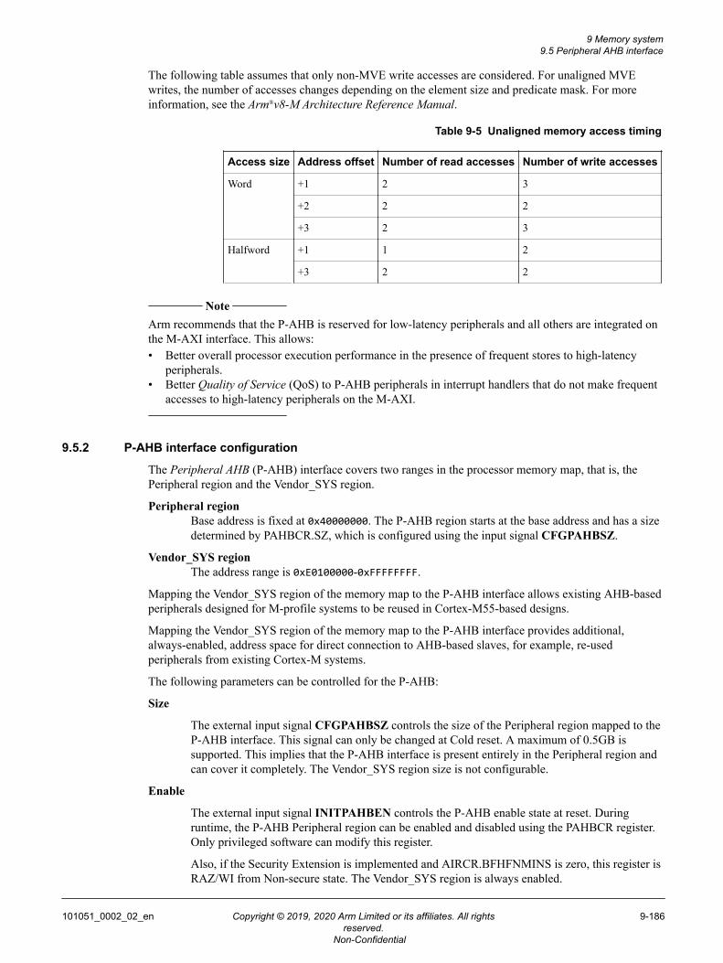
The following table assumes that only non-MVE write accesses are considered. For unaligned MVEwrites, the number of accesses changes depending on the element size and predicate mask. For moreinformation, see the Arm®v8-M Architecture Reference Manual.
Table 9-5 Unaligned memory access timing
Access size Address offset Number of read accesses Number of write accesses
Word +1 2 3
+2 2 2
+3 2 3
Halfword +1 1 2
+3 2 2
Note
Arm recommends that the P-AHB is reserved for low-latency peripherals and all others are integrated onthe M-AXI interface. This allows:• Better overall processor execution performance in the presence of frequent stores to high-latency
peripherals.• Better Quality of Service (QoS) to P-AHB peripherals in interrupt handlers that do not make frequent
accesses to high-latency peripherals on the M-AXI.
9.5.2 P-AHB interface configuration
The Peripheral AHB (P-AHB) interface covers two ranges in the processor memory map, that is, thePeripheral region and the Vendor_SYS region.
Peripheral regionBase address is fixed at 0x40000000. The P-AHB region starts at the base address and has a sizedetermined by PAHBCR.SZ, which is configured using the input signal CFGPAHBSZ.
Vendor_SYS regionThe address range is 0xE0100000-0xFFFFFFFF.
Mapping the Vendor_SYS region of the memory map to the P-AHB interface allows existing AHB-basedperipherals designed for M-profile systems to be reused in Cortex-M55-based designs.
Mapping the Vendor_SYS region of the memory map to the P-AHB interface provides additional,always-enabled, address space for direct connection to AHB-based slaves, for example, re-usedperipherals from existing Cortex‑M systems.
The following parameters can be controlled for the P-AHB:
Size
The external input signal CFGPAHBSZ controls the size of the Peripheral region mapped to theP-AHB interface. This signal can only be changed at Cold reset. A maximum of 0.5GB issupported. This implies that the P-AHB interface is present entirely in the Peripheral region andcan cover it completely. The Vendor_SYS region size is not configurable.
Enable
The external input signal INITPAHBEN controls the P-AHB enable state at reset. Duringruntime, the P-AHB Peripheral region can be enabled and disabled using the PAHBCR register.Only privileged software can modify this register.
Also, if the Security Extension is implemented and AIRCR.BFHFNMINS is zero, this register isRAZ/WI from Non-secure state. The Vendor_SYS region is always enabled.
9 Memory system9.5 Peripheral AHB interface
101051_0002_02_en Copyright © 2019, 2020 Arm Limited or its affiliates. All rightsreserved.
9-186
Non-Confidential
Alias
The P-AHB interface supports the ability to alias two logical addresses in the Peripheral regiononto the P-AHB interface. This feature is used with an external security gate to support fine-grain Secure and Non-secure regions in the Peripheral region. The alias bit in the logical addresscan be configured from bit[24] to bit[28] using the external input signal CFGMEMALIAS.This signal can only be changed at reset.
Data accesses to the P-AHB Peripheral region are performed on the Master AXI (M-AXI) interface whenthe P-AHB interface is disabled. Accesses to the Peripheral region above the P-AHB size limit is alsoperformed on the M-AXI interface.
Instruction accesses made to the Peripheral region, where executable, are always performed on the M-AXI interface. For code portability, Arm recommends that the P-AHB region is programmed as ExecuteNever (XN) in the Memory Protection Unit (MPU) to prevent instruction execution. This is consistentwith the default memory map. The Vendor_SYS region is permanently XN.
9.5.3 P-AHB considerations
Normal memory is supported on the Peripheral AHB (P-AHB) interface. However, no Normal-specificoptimizations are made. This means the interface is generally not suitable for high-bandwidthrequirements, and the Tightly Coupled Memory (TCM) or Master AXI (M-AXI) interfaces must be usedinstead.
Instruction execution and vector fetches are not supported on this interface. The P-AHB is targeted at on-chip peripherals only.
The amount of buffering resource is intentionally limited to provide a balance between load accesslatency and store throughput. The implications of this limited buffering are:• Individual stores to the P-AHB interface are visible to the Device memory in minimal and
deterministic time relative to the store instruction being executed. This is relevant, for example, whenan interrupt handler must perform a critical device access.
• There is limited hiding of store latency from the pipeline. This means that high-latency peripheralscan stall the pipeline on a store instruction for extended periods of time. However, it affects theoverall processor execution performance.
• Loads to the P-AHB interface are inherently higher latency than stores and must wait for all bufferedstores to drain before they can be started on the bus. The limited buffering means that this latency isminimized but can still be significant for high-latency peripherals. The pipeline cannot flush a loadthat has started on the bus. Therefore, interrupt latency is affected by wait-states on loads. However,loads that have not yet started on the bus can be safely flushed. Therefore, the impact of load wait-states on interrupt latency is limited to the wait-states on a single access.
• Load access throughput is limited. There is no support for bursts on load multiples and no support forpipelined loads in general.
• Store throughput is acceptable for zero wait state systems, but it is degraded when wait states areused.
9 Memory system9.5 Peripheral AHB interface
101051_0002_02_en Copyright © 2019, 2020 Arm Limited or its affiliates. All rightsreserved.
9-187
Non-Confidential
9.6 S-AHB interfaceThe 64-bit Slave-AHB (S-AHB) interface provides system access to the Tightly Coupled Memories(TCMs). Typically, a Direct Memory Access (DMA) controller uses this interface to transfer data in andout of the processor for software computation. It includes arbitration logic to support simultaneoussystem and processor TCM access requests. The S-AHB interface implements the AMBA 5 AHBprotocol.
If there is no contention with software access to TCM and the TCM uses zero wait states, then writebuffering and the read prefetcher allows the S-AHB interface to indefinitely sustain back-to-back writeand read transactions.
Write buffering
Writes are buffered in the S-AHB interface to improve system performance and to provide storage forsplitting 64-bit writes into two separate 32-bit transactions to the TCM interfaces.
Read access latency is inherently larger than write access latency because the AHB interface can onlysupport a single outstanding transaction. To minimize this latency, reads can overtake buffered writes.However, if there is a data dependency between a read and a buffered write, then hazarding logic stallsthe read and attempts to drain the buffer until there are no longer any dependencies. Writes are alwayscarried out in-order and hazarding is performed at byte granularity.
Additional hazarding is included to fully serialize read accesses to the TCM from the S-AHB interfaceand software running on the processor. This allows both masters to access the TCM coherently. For moreinformation on how data can be shared between software running on the processor and system-leveldevices that are connected on the S-AHB interface, see 9.8.5 System access to TCM through the S-AHBDMA interface on page 9-194.
Read prefetcherThe S-AHB interface also supports a read prefetcher to improve the performance of the processor whilereading bursts of data from the TCM to the system. The prefetcher supports the following 64-bit and 32-bit read transfers:• INCR.• INCR4.• INCR8.• INCR16.
If there is no contention or wait states on the TCM banks being accessed, the prefetcher generatesinternal transactions so that read data can be returned on consecutive clock cycles on the S-AHBinterface.
Note
• The S-AHB interface supports an extension to the AHB5 protocol using byte-lane strobe signals toefficiently handle data with non-contiguous write-data in a beat, similar to that supported on AMBAAXI interfaces. This allows for efficient bridging from an AXI-based DMA controller.
• All S-AHB accesses are treated as being the same endianness as memory. No data swizzling isperformed for reads or writes.
• The S-AHB interface can be used even if the processor is in sleep mode.
9.6.1 S-AHB memory map
The memory map that is presented on the Slave-AHB (S-AHB) interface is consistent with the memorymap that is presented to software running on the processor. Only the Tightly Coupled Memory (TCM)address range can be accessed. Any other addresses cause an AHB fault response.
9 Memory system9.6 S-AHB interface
101051_0002_02_en Copyright © 2019, 2020 Arm Limited or its affiliates. All rightsreserved.
9-188
Non-Confidential
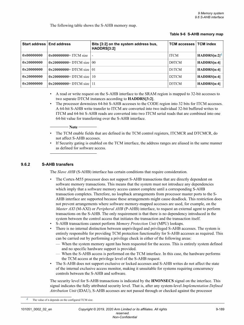
The following table shows the S-AHB memory map.
Table 9-6 S-AHB memory map
Start address End address Bits [3:2] on the system address bus,HADDRS[3:2]
TCM accesses TCM index
0x00000000 0x00000000+ ITCM size - ITCM HADDRS[n:2]d
0x20000000 0x20000000+ DTCM size 00 D0TCM HADDRS[n:4]
0x20000000 0x20000000+ DTCM size 01 D1TCM HADDRS[n:4]
0x20000000 0x20000000+ DTCM size 10 D2TCM HADDRS[n:4]
0x20000000 0x20000000+ DTCM size 11 D3TCM HADDRS[n:4]
• A read or write request on the S-AHB interface to the SRAM region is mapped to 32-bit accesses totwo separate DTCM instances according to HADDRS[3:2].
• The processor downsizes 64-bit S-AHB accesses to the CODE region into 32 bits for ITCM accesses.A 64-bit S-AHB write transfer to ITCM are converted into two individual 32-bit buffered writes toITCM and 64-bit S-AHB reads are converted into two ITCM serial reads that are combined into one64-bit value for transferring over the S-AHB interface.
Note
• The TCM enable fields that are defined in the TCM control registers, ITCMCR and DTCMCR, donot affect S-AHB accesses.
• If Security gating is enabled on the TCM interface, the address ranges are aliased in the same manneras defined for software access.
9.6.2 S-AHB transfers
The Slave AHB (S-AHB) interface has certain conditions that require consideration.
• The Cortex-M55 processor does not support S-AHB transactions that are directly dependent onsoftware memory transactions. This means that the system must not introduce any dependencieswhich imply that a software memory access cannot complete until a corresponding S-AHBtransaction completes. Therefore, no loopback arrangements from processor master ports to the S-AHB interface are supported because these arrangements might cause deadlock. This restriction doesnot prevent arrangements where software memory-mapped accesses are used, for example, on theMaster AXI (M-AXI) or Peripheral AHB (P-AHB) interface, to request an external agent to performtransactions on the S-AHB. The only requirement is that there is no dependency introduced in thesystem between the control access that initiates the transaction and the transaction itself.
• S-AHB transactions cannot perform Memory Protection Unit (MPU) lookups.• There is no internal distinction between unprivileged and privileged S-AHB accesses. The system is
entirely responsible for providing TCM protection functionality for S-AHB accesses as required. Thiscan be carried out by performing a privilege check in either of the following areas:— When the system memory agent has been requested for the access. This is entirely system defined
and no specific hardware support is provided.— When the S-AHB access is performed on the TCM interface. In this case, the hardware performs
the TCM access at the privilege level of the S-AHB request.• The S-AHB does not support exclusive or locked accesses and S-AHB writes do not affect the state
of the internal exclusive access monitor, making it unsuitable for systems requiring concurrencycontrols between the S-AHB and software.
The security level for S-AHB transactions is indicated by the HNONSECS signal on the interface. Thissignal indicates the fully attributed security level. That is, after any system-level Implementation DefinedAttribution Unit (IDAU), S-AHB accesses are not passed through or checked against the processor
d The value of n depends on the configured TCM size.
9 Memory system9.6 S-AHB interface
101051_0002_02_en Copyright © 2019, 2020 Arm Limited or its affiliates. All rightsreserved.
9-189
Non-Confidential
IDAU or Security Attribution Unit (SAU). The TCM security gate can be used to control access to theTCM based on the transaction security level.
Note
• INCR is an incrementing burst, where the address for each transfer in the burst is an increment of theaddress for the previous transfer.
• For more information on burst types, see the Arm® AMBA® 5 AHB Protocol Specification.
For more information on TCM security gating, see 8.8 TCM and P-AHB security access controlon page 8-165.
9.6.3 S-AHB interface arbitration
In normal operation, there is enough bandwidth across the four Data Tightly Coupled Memory (DTCM)interfaces to allow accesses from software and the Slave AHB (S-AHB) interface to sustain theirmaximum throughput and the Instruction Tightly Coupled Memory (ITCM) is normally only used forinstruction fetch. This means contention for resource should be rare and so the S-AHB is usually thelowest priority with no impact on the performance of data transfer from the system to the TCM.
However, there might be cases when a source makes large numbers of accesses to the same TCM bank.To prevent the S-AHB interface from getting less bandwidth, the priority of a request on the interface isautomatically boosted when there is contention with a software access. When this occurs, a round robinscheme is used to share the bandwidth to a TCM bank roughly equally between S-AHB accesses andsoftware accesses. This also allows the TCM bandwidth to be split evenly between software and S-AHBtransactions if contention occurs.
9.6.4 S-AHB availability and low power states
The following conditions are required for the S-AHB to accept transactions:
• The processor power domain (PDCORE) is active and not in reset.• CLKIN is running.
The S-AHB sub-system and the TCMs are in a separate internal clock domain to the rest of theprocessor. However, they are in the same reset and power domains. Therefore, S-AHB transactions canbe performed without the main internal processor clock running. This allows TCM data transfers to beoffloaded to a low-power system agent while the processor is in any of its sleep modes. The TCM clockis gated inside the processor to minimize the power used when no transactions are in progress from eitherthe processor or S-AHB. Asserting HTRANSS automatically starts the clock if it is gated and the clockis stopped after all outstanding transactions have completed. For more information on HTRANSS, seeC.10 S-AHB interface signals on page Appx-C-392
Note
From a system perspective, you are responsible to ensure that CLKIN is running when a transaction isstarted on S-AHB by considering the requirements of any master components which can access the slaveinterface, for example a DMA, and enabling system level clock gating accordingly. This might meanoverriding the current CLKINQACTIVE state if the processor is in sleep and so not requesting CLKIN.
9 Memory system9.6 S-AHB interface
101051_0002_02_en Copyright © 2019, 2020 Arm Limited or its affiliates. All rightsreserved.
9-190
Non-Confidential
9.7 EPPB interfaceThe External Private Peripheral Bus (EPPB) interface is a 32-bit AMBA 4 APB interface designed forintegration with CoreSight debug and trace components.
It is used for data accesses to the memory region 0xE0040000-0xE00FEFFF. Instruction accesses to thisregion cause a fault, and are permanently disabled in the Armv8.1‑M architecture.
The interface is not intended for general peripheral usage and has both higher latency and lower averagethroughput than the Master AXI (M-AXI) or Peripheral AHB (P-AHB) interfaces. Additionally, it has thefollowing limitations that make it unsuitable for general-purpose use:
• Only little-endian accesses are supported. This indicates that the processor endianness is ignored.• All accesses are treated as Device transactions.• Only aligned accesses are supported. Unaligned accesses to the EPPB interface cause an
UNALIGNED UsageFault.• Exclusive accesses are not supported.• Only Privileged accesses are supported. Unprivileged accesses take a BusFault exception.
Arm recommends that all non-debug peripherals are integrated on the M-AXI or P-AHB interface.
The EPPB interface can perform debugger-initiated transactions during processor reset. The EPPBinterface can also be extended to support interface protection between the processor and the interconnect.For more information on interface protection, see 10.3 Interface protection behavior on page 10-219.
For more information, see 14.2.4 Debug during reset and before code execution commenceson page 14-263.
Additionally, for more information on EPPB peripherals, see 7.3 Private Peripheral Bus on page 7-148.
The EPPB interface is also used to transfer Nested Vectored Interrupt Controller (NVIC) state to anExternal Wakeup Interrupt Controller (EWIC) on sleep entry and exit. For more information on EWICsleep entry and exit, see the Arm® Cortex®-M55 Processor Integration and Implementation Manual.
Note
The Arm® Cortex®-M55 Processor Integration and Implementation Manual is a confidential documentthat is only available to Cortex-M55 processor IP licensees.
9 Memory system9.7 EPPB interface
101051_0002_02_en Copyright © 2019, 2020 Arm Limited or its affiliates. All rightsreserved.
9-191
Non-Confidential
9.8 TCM interfacesThe Tightly Coupled Memory (TCM) interfaces are tightly coupled into the processor for optimumperformance from fast on-chip memory.
The Cortex-M55 processor supports two separate interface groups:
ITCMSingle 32-bit interface that is intended for instruction memory based on SRAM or potentiallyflash memory with system prefetch or acceleration.
DTCMFour 32-bit interfaces intended for use with data memory that is expected to be based on SRAM.The Cortex-M55 processor performs address filtering that is based on bits[3:2] of the address.• Addresses with bit[3:2]=0b00 are performed on the D0TCM interface.• Addresses with bit[3:2]=0b01 are performed on the D1TCM interface.• Addresses with bit[3:2]=0b10 are performed on the D2TCM interface.• Addresses with bit[3:2]=0b11 are performed on the D3TCM interface.
This configuration requires that the DTCM RAM is logically arranged into four separate addressbanks. This allows:• Up to 128 bits of total bandwidth for software reads and writes, and Direct Memory Access
(DMA) traffic through the Slave AHB (S-AHB) interface with a probabilistic reduction ofcontention. This is essential for compute performance because the Cortex-M55 processorcan sustain a data throughput of 64 bits per cycle using the M-class Vector Extension (MVE)instructions.
• A 64-bit bandwidth for contiguous accesses that are 32-bit aligned from the software andDMA. A 64-bit bandwidth for contiguous accesses is essential for both overall performanceand interrupt latency.
• Dual-issuing of 32-bit (or lower) aligned read or write transactions to the DTCM fromsoftware, where the two addresses do not contend. The MVE scatter gather load/storeinstructions can generate these operations.
Note
• The Cortex-M55 processor does not provide software control over address filtering.• All TCM interfaces support wait and error response from external memory. For systems where
functional safety or Reliability, Availability, and Serviceability (RAS) are required, the Cortex-M55processor also optionally supports a Single Error Correction and Double Error Detection (SECDED)scheme that is based on the Error Correcting Code (ECC) for all accesses in the ITCM and DTCMregions.
9.8.1 TCM configuration
The TCM interface has fixed and configurable parameters.
The base address of each TCM is fixed:
ITCM0x00000000. This is the base address of the Code region.
DTCM0x20000000. This is the base address of the SRAM region.
The following parameters can be separately controlled for each of the TCMs:
9 Memory system9.8 TCM interfaces
101051_0002_02_en Copyright © 2019, 2020 Arm Limited or its affiliates. All rightsreserved.
9-192
Non-Confidential
Size External configuration input signals control the size of each TCM region. These signals canonly be changed at Cold reset. A maximum of 16MB for each TCM is supported. This impliesthat the ITCM and DTCM are present entirely in the Code and SRAM regions of the memorymap respectively.
Enable An external input signal controls the TCM enable state at reset. During runtime the TCM canbe enabled and disabled using the ITCMCR and DTCMCR registers. Only privileged softwarecan modify these registers. If the Security Extension is implemented and AIRCR.BFHFNMINSis zero, these registers are RAZ/WI from Non-secure state.
Alias The TCM controller can alias two logical addresses in the Code and SRAM regions onto theITC and DTCM interface respectively. This feature is used with the TCM security gate tosupport fine-grain Secure and Non-secure regions in TCM memory. The alias bit in the logicaladdress can be configured from bit[24] to bit[28] using the external input signalCFGMEMALIAS. This signal can only be changed at Cold reset.
Note
• For more information on ITCMCR and DTCMCR registers, see 4.19 ITCMCR and DTCMCR, TCMControl Registers on page 4-101.
• For more information on AIRCR, see the Arm®v8-M Architecture Reference Manual.• Address aliasing and security gating are described in 8.8 TCM and P-AHB security access control
on page 8-165.
9.8.2 TCM transactions
TCM regions are implicitly Normal, Non-shareable, Non-cacheable memory.
For TCM memory regions, the Cortex-M55 processor:
• Ignores the Memory Protection Unit (MPU) memory type attributes that software assigns. The MPUprotection settings are always considered.
• Initiates Speculative reads. You must not assume that the scope of this speculation is fixed, or that itcan be definitively specified. For example, speculation might occur:— For instruction prefetching, depending on the recent execution stream.— For data reads that are performed before the Security or MPU protection settings are evaluated.
Although the access might be performed speculatively, an abort is subsequently raised if requiredby the Security or MPU protection settings.
— For data reads in branch shadows.• Buffers data on writes. Read transactions always hazard against outstanding buffered write
transactions to the same address. Writes transactions are never Speculative.
This behavior makes TCMs unsuitable for peripherals or any memory that has implications for readtransactions. Devices of this type must be integrated on the Peripheral AHB (P-AHB) or Master-AXI (M-AXI) interfaces. These interfaces support the Device memory type. Additionally, the following accessesare performed on the M-AXI interface instead of the TCM interfaces:• Accesses to TCM regions when the relevant TCM is disabled.• Accesses to the Code and SRAM regions above the TCM size limit, regardless of the TCM enable.
For code portability to other Arm processors or systems, Arm recommends that TCM regions are alwaysdefined as Normal, Non-shareable memory in the MPU.
This is consistent with the default memory map attributes which apply when the MPU is either disabledor not implemented.
9.8.3 Booting from TCM
The Cortex-M55 processor provides support for booting from volatile TCM memory that must beinitialized at reset.
9 Memory system9.8 TCM interfaces
101051_0002_02_en Copyright © 2019, 2020 Arm Limited or its affiliates. All rightsreserved.
9-193
Non-Confidential
The TCMs can be enabled out of reset without software programming. When the CPUWAIT signal thatstalls the core is HIGH out of reset, it prevents the processor from executing any software at the resetvector. This allows the TCMs to be loaded by the system before the processor performs any TCMaccesses. When the TCM loading sequence is complete, this signal can be deasserted to allow theprocessor to boot up. The Slave AHB (S-AHB) Direct Memory Access (DMA) interface is functionalwhen the CPUWAIT signal that stalls the core is asserted out of reset and can therefore servicetransactions that the system initiates to load the TCMs. This avoids the need for external hardware on theTCM interface for boot-time initialization.
Note
Asserting CPUWAIT prevents the processor from reading the stack pointer (SP) or initial programcounter (PC) from the reset vector. Therefore, it is safe to load the vector table, code, and data into theTCM. Alternatively, the external input signals INITSVTOR and INITNSVTOR can be used to set thevector table address in non-volatile memory.
When ECC is enabled, before performing a byte, halfword, or unaligned word write to a TCM locationwhich causes an RMW, you must initialize the location first by performing an aligned word ordoubleword write to the location. Arm recommends that all TCM locations are initialized in this mannerby boot code.
9.8.4 Integration with flash memory
The Cortex-M55 processor can support the use of flash memory connected to Tightly Coupled Memory(TCM). The Instruction Tightly Coupled Memory (ITCM) interface is most suitable for this arrangement.
The system must take into account the fetch bandwidth requirements for efficient code execution by theprocessor. The processor can consume up to 32 bits of instruction data per cycle using both 32-bit Thumband 16-bit Thumb instructions, because the 16-bit Thumb instructions can be dual-issued. The overallbandwidth is specific to your application but for general-purpose products, it must be assumed that 32bits per cycle might be required. The instruction memory system needs to sustain this for maximumperformance. Arm recommends that if flash memory is integrated on the ITCM, some system cache orFlash accelerator is used to meet these fetch bandwidth requirements.
Alternatively, flash memory can be integrated on the Master AXI (M-AXI) and the processor can beconfigured to include an L1 instruction cache.
9.8.5 System access to TCM through the S-AHB DMA interface
The 64-bit Slave-AHB (S-AHB) interface provides system access to the Tightly Coupled Memory (TCM)even when the Cortex-M55 processor is running.
Typically, this feature is used with a Direct Memory Access (DMA) controller to transfer data to andfrom the processor for compute applications. Arbitration between processor access from software and S-AHB requests to TCM is fully supported with no requirement for external TCM interface logic. For moreinformation on this arbitration logic, see 9.6.3 S-AHB interface arbitration on page 9-190.
There is no hardware support for concurrency control between software and S-AHB access to TCM.Particularly, software exclusive accesses to TCM are only subject to the internal exclusive monitor whichdoes not take S-AHB accesses into consideration. This implies that the system must not perform S-AHBaccesses to any regions of TCM memory that are used with software exclusive accesses. However, it ispossible in software to share data coherently between the executing thread and the S-AHB interface. Theprocessor makes the following hardware guarantees to share data coherently:• Appropriate writes to the TCM by software and S-AHB are never repeated. Store double instructions,
floating-point store multiple instructions storing double-precision values, M‑profile Vector Extension(MVE) stores, and unaligned single stores can be repeated on exception return. Therefore, these
9 Memory system9.8 TCM interfaces
101051_0002_02_en Copyright © 2019, 2020 Arm Limited or its affiliates. All rightsreserved.
9-194
Non-Confidential
transactions are exempt from this guarantee and unsuitable for software synchronization. Theprocessor guarantees that no single-copy-atomic access is repeated.
• Software and S-AHB writes to the TCM have a single point of serialization which is the TCMControl Unit (TCU). This means that when a write is observable by one master, it is guaranteed to beobservable by the other.
• When a write on the S-AHB interface is accepted, the processor assumes responsibility for thecoherent observation of that data. Any read by any master interface that is initiated after the S-AHBwrite completed returns the updated data.
Note
• TCMs are implicitly Normal memory, therefore, write buffering is permitted.• All TCU buffers are drained before the processor enters a low-power sleep state.
The following table shows an example software sequence for message passing between coherentcomponents in a system.
Table 9-7 Example software sequence for message passing between coherent components in a system
Data generator Data consumer
STR <data> LDR <valid>
STL <valid> : Store-release LOOP until <valid> set
LDA <data> : Load acquire
The S-AHB interface always performs writes in-order, and therefore, it does not need a barrier whengenerating data into the TCM.
Interrupt-based synchronization is also possible in the Cortex-M55 processor when the S-AHB is thedata generator. In this model, an interrupt is generated when the last data transfer completes on theexternal interface. The first instruction in the Interrupt Service Routine (ISR) is guaranteed to observeany data items that are stored before or on this transfer. In this case, the completion of the last S-AHBaccess is used to indicate global observability instead of performing a software read of the location andwaiting until it has been updated.
For more information on the S-AHB interface, see 9.6 S-AHB interface on page 9-188.
9 Memory system9.8 TCM interfaces
101051_0002_02_en Copyright © 2019, 2020 Arm Limited or its affiliates. All rightsreserved.
9-195
Non-Confidential
9.9 Instruction and data cacheThe Cortex-M55 processor supports optional, internal L1 Harvard caches for high performance operationusing on-chip or external memory.
Only the Master-AXI (M-AXI) interface accesses can be cached. TCM and Peripheral AHB (P-AHB)interface transactions or accesses cannot be cached.
To enable software to appropriately deal with different levels of cache, the cache maintenance operationscan perform up to the following points:
Point of Unification (PoU)This is the point at which the instruction and data caches can see the same copy of a memorylocation. For the Cortex-M55 processor:• When either an L1 data cache or an instruction cache is included, the PoU is always at the
system level, therefore, cache maintenance operations by address always act on the L1cache. This is indicated by CLIDR.LoUU and CLIDR.LoUIS bitfields. This implies that thedata and instruction cache accesses are unified at the system level.
• When the data cache and instruction cache are excluded, the CLIDR.LoUU andCLIDR.LoUIS bits are 0b000.
Point of Coherency (PoC)This is the point at which all components that can access memory can see the same copy of amemory location. For the Cortex-M55 processor:• When either an L1 data cache or instruction cache is included, the PoC is always at the
system level, therefore, cache maintenance operations by address always act on the L1cache. This is indicated by CLIDR.LoC bit field. This implies that data accesses are coherentat the system level or beyond the system level.
• When the L1 data cache and instruction cache are excluded, the CLIDR.LoC bit is 0b000.
For more information on the CLIDR register, see 4.5.1 CLIDR, Cache Level ID Register on page 4-62.
Each cache can be independently configured within the following range:• 4KB• 8KB• 16KB• 32KB• 64KB
Both the L1 instruction cache and data caches store the valid bits for each cache line in RAM. TheCortex-M55 processor provides a hardware mechanism to invalidate the cache at reset. This mechanismcan be disabled to maintain valid cache state across reset, for example, where the RAM supports dataretention and the processor logic is reset after powerup.
The automatic invalidation sequence can take a large number of cycles and executes independently of theinstructions that are running on the processor. While the automatic invalidation sequence is in progress,any cache maintenance operation is treated as a NOP and instructions and data accesses do not look up inthe cache. A DSB instruction waits for all automatic cache invalidate sequences to complete.
Software can also be used to perform a complete invalidation before enabling the data cache on reset.The L1 instruction cache can be invalidated by a single instruction but the L1 data cache needs a loopiterating through all entries.
The architecture specifies the cache maintenance operations which can be used by software. The Cortex-M55 processor includes memory-mapped registers that allow software to examine the content of thecache tag and data RAMs directly. This can be used for profiling or debugging the cache content. See4.11 Direct cache access registers on page 4-75 for more information. The Direct Cache Access registersare only accessible in Secure state. Therefore, there is no requirement to restrict cache readability. Theprocessor supports direct access to the cache RAM, therefore, access to the L1 instruction cache must
9 Memory system9.9 Instruction and data cache
101051_0002_02_en Copyright © 2019, 2020 Arm Limited or its affiliates. All rightsreserved.
9-196
Non-Confidential
also be restricted. This can be achieved by asserting the external input signal LOCKDCAIC. For moreinformation on LOCKDCAIC, see C.27 Miscellaneous signals on page Appx-C-413.
Dirty data must be written back to external memory before the processor and RAM are powered downbecause the L1 data cache supports write-back operation.
All cache RAMs are standard single-ported RAMs and can be generated using standard RAM compilers.
9.9.1 L1 data cache
The Cortex-M55 processor L1 data cache has the following features:
• It is a four-way set-associative cache.• It has a cache line size of 32 bytes.• It supports the following inner memory attributes and allocation hints for Non-shareable memory:
— Write-Back and Write-Through Cacheable.— Read-Allocate and No Read-Allocate.— Write-Allocate and No Write-Allocate.— Transient and Non-transient. Clean cache lines that are associated with Transient memory are
prioritized for eviction over lines that are associated with Non-transient memory.
Allocation into the L1 data cache depends on inner memory attributes only.• The outer and inner memory attributes are exported on the Master AXI (M-AXI) interface to support
further system-level caching.• The Shareability attribute forces the region to be treated as Non-cacheable, regardless of the inner
memory attributes. This enables maintaining coherency at the system-level.
Software or a debugger might use the direct cache access registers to read the contents of RAM arrays.The data cache is logically organized into two sets of RAM arrays. The dimensions of these RAM arraysvary with the cache size and the inclusion of Error Correcting Code (ECC) logic.
Table 9-8 Data cache RAM organization
Array Number ofcacheinstances
Datastored
Writegranularity
Array widthexcluding ECC(bits)
Array widthincluding ECC(bits)
Array depth(number of entries)
4KB 64KB 4KB 64KB 4KB 64KB
Tag 4 Tag, valid,line status
RAM word 26 22 33 29 32 512
Data 8 Data Byte 32 32 39 39 128 2048
No Write-Allocate mode
When a memory region is marked as Cacheable Write-Allocate, it normally allocates a cache line on awrite miss. However, there are some situations where allocating on writes is undesirable, such asexecuting the C standard library memset() function to clear a large block of memory to a known value.
Writing large blocks of data like this can pollute the cache with unnecessary data. It can also waste powerand performance if a linefill must be performed only to discard the linefill data because the entire linewas subsequently written by the memset().
To prevent this, the Cortex-M55 data cache includes logic to automatically disable data cache allocationon a write miss when streaming behavior is detected. When in this mode, writes are buffered and thenwritten directly out to the external system through the Master-AXI (M-AXI) interface even if they arecacheable.
9 Memory system9.9 Instruction and data cache
101051_0002_02_en Copyright © 2019, 2020 Arm Limited or its affiliates. All rightsreserved.
9-197
Non-Confidential
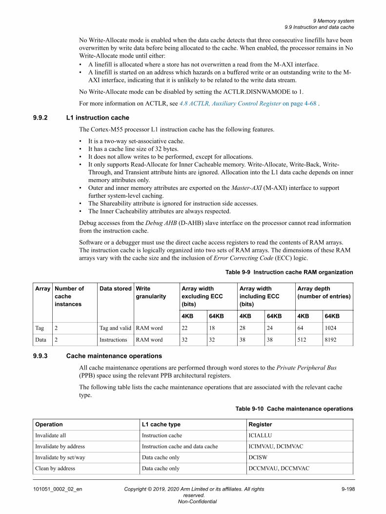
No Write-Allocate mode is enabled when the data cache detects that three consecutive linefills have beenoverwritten by write data before being allocated to the cache. When enabled, the processor remains in NoWrite-Allocate mode until either:• A linefill is allocated where a store has not overwritten a read from the M-AXI interface.• A linefill is started on an address which hazards on a buffered write or an outstanding write to the M-
AXI interface, indicating that it is unlikely to be related to the write data stream.
No Write-Allocate mode can be disabled by setting the ACTLR.DISNWAMODE to 1.
For more information on ACTLR, see 4.8 ACTLR, Auxiliary Control Register on page 4-68 .
9.9.2 L1 instruction cache
The Cortex-M55 processor L1 instruction cache has the following features.
• It is a two-way set-associative cache.• It has a cache line size of 32 bytes.• It does not allow writes to be performed, except for allocations.• It only supports Read-Allocate for Inner Cacheable memory. Write-Allocate, Write-Back, Write-
Through, and Transient attribute hints are ignored. Allocation into the L1 data cache depends on innermemory attributes only.
• Outer and inner memory attributes are exported on the Master-AXI (M-AXI) interface to supportfurther system-level caching.
• The Shareability attribute is ignored for instruction side accesses.• The Inner Cacheability attributes are always respected.
Debug accesses from the Debug AHB (D-AHB) slave interface on the processor cannot read informationfrom the instruction cache.
Software or a debugger must use the direct cache access registers to read the contents of RAM arrays.The instruction cache is logically organized into two sets of RAM arrays. The dimensions of these RAMarrays vary with the cache size and the inclusion of Error Correcting Code (ECC) logic.
Table 9-9 Instruction cache RAM organization
Array Number ofcacheinstances
Data stored Writegranularity
Array widthexcluding ECC(bits)
Array widthincluding ECC(bits)
Array depth(number of entries)
4KB 64KB 4KB 64KB 4KB 64KB
Tag 2 Tag and valid RAM word 22 18 28 24 64 1024
Data 2 Instructions RAM word 32 32 38 38 512 8192
9.9.3 Cache maintenance operations
All cache maintenance operations are performed through word stores to the Private Peripheral Bus(PPB) space using the relevant PPB architectural registers.
The following table lists the cache maintenance operations that are associated with the relevant cachetype.
Table 9-10 Cache maintenance operations
Operation L1 cache type Register
Invalidate all Instruction cache ICIALLU
Invalidate by address Instruction cache and data cache ICIMVAU, DCIMVAC
Invalidate by set/way Data cache only DCISW
Clean by address Data cache only DCCMVAU, DCCMVAC
9 Memory system9.9 Instruction and data cache
101051_0002_02_en Copyright © 2019, 2020 Arm Limited or its affiliates. All rightsreserved.
9-198
Non-Confidential
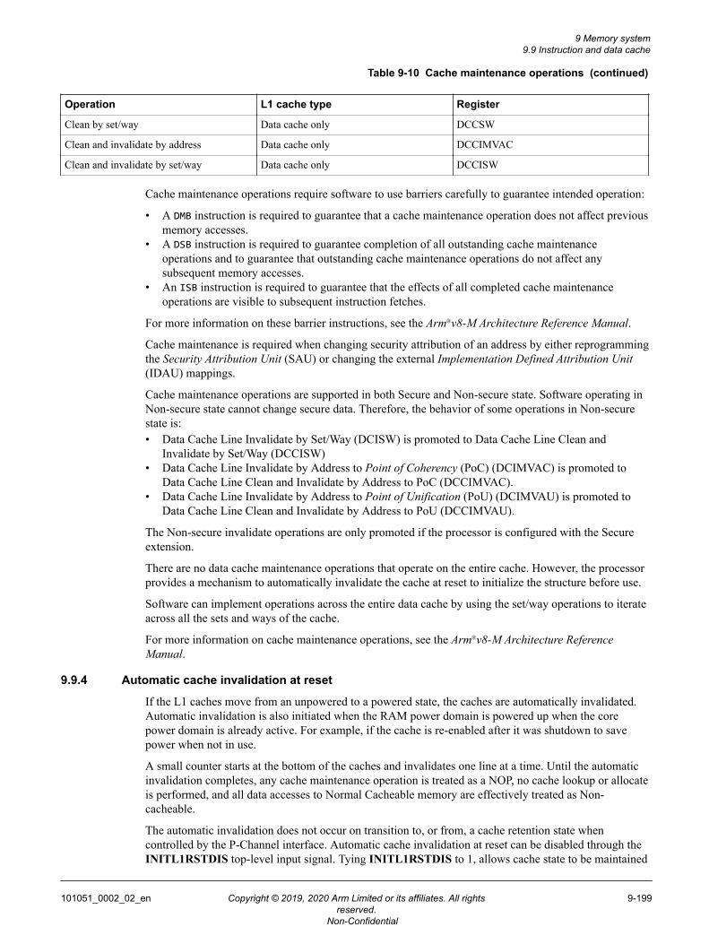
Table 9-10 Cache maintenance operations (continued)
Operation L1 cache type Register
Clean by set/way Data cache only DCCSW
Clean and invalidate by address Data cache only DCCIMVAC
Clean and invalidate by set/way Data cache only DCCISW
Cache maintenance operations require software to use barriers carefully to guarantee intended operation:
• A DMB instruction is required to guarantee that a cache maintenance operation does not affect previousmemory accesses.
• A DSB instruction is required to guarantee completion of all outstanding cache maintenanceoperations and to guarantee that outstanding cache maintenance operations do not affect anysubsequent memory accesses.
• An ISB instruction is required to guarantee that the effects of all completed cache maintenanceoperations are visible to subsequent instruction fetches.
For more information on these barrier instructions, see the Arm®v8-M Architecture Reference Manual.
Cache maintenance is required when changing security attribution of an address by either reprogrammingthe Security Attribution Unit (SAU) or changing the external Implementation Defined Attribution Unit(IDAU) mappings.
Cache maintenance operations are supported in both Secure and Non-secure state. Software operating inNon-secure state cannot change secure data. Therefore, the behavior of some operations in Non-securestate is:• Data Cache Line Invalidate by Set/Way (DCISW) is promoted to Data Cache Line Clean and
Invalidate by Set/Way (DCCISW)• Data Cache Line Invalidate by Address to Point of Coherency (PoC) (DCIMVAC) is promoted to
Data Cache Line Clean and Invalidate by Address to PoC (DCCIMVAC).• Data Cache Line Invalidate by Address to Point of Unification (PoU) (DCIMVAU) is promoted to
Data Cache Line Clean and Invalidate by Address to PoU (DCCIMVAU).
The Non-secure invalidate operations are only promoted if the processor is configured with the Secureextension.
There are no data cache maintenance operations that operate on the entire cache. However, the processorprovides a mechanism to automatically invalidate the cache at reset to initialize the structure before use.
Software can implement operations across the entire data cache by using the set/way operations to iterateacross all the sets and ways of the cache.
For more information on cache maintenance operations, see the Arm®v8-M Architecture ReferenceManual.
9.9.4 Automatic cache invalidation at reset
If the L1 caches move from an unpowered to a powered state, the caches are automatically invalidated.Automatic invalidation is also initiated when the RAM power domain is powered up when the corepower domain is already active. For example, if the cache is re-enabled after it was shutdown to savepower when not in use.
A small counter starts at the bottom of the caches and invalidates one line at a time. Until the automaticinvalidation completes, any cache maintenance operation is treated as a NOP, no cache lookup or allocateis performed, and all data accesses to Normal Cacheable memory are effectively treated as Non-cacheable.
The automatic invalidation does not occur on transition to, or from, a cache retention state whencontrolled by the P-Channel interface. Automatic cache invalidation at reset can be disabled through theINITL1RSTDIS top-level input signal. Tying INITL1RSTDIS to 1, allows cache state to be maintained
9 Memory system9.9 Instruction and data cache
101051_0002_02_en Copyright © 2019, 2020 Arm Limited or its affiliates. All rightsreserved.
9-199
Non-Confidential
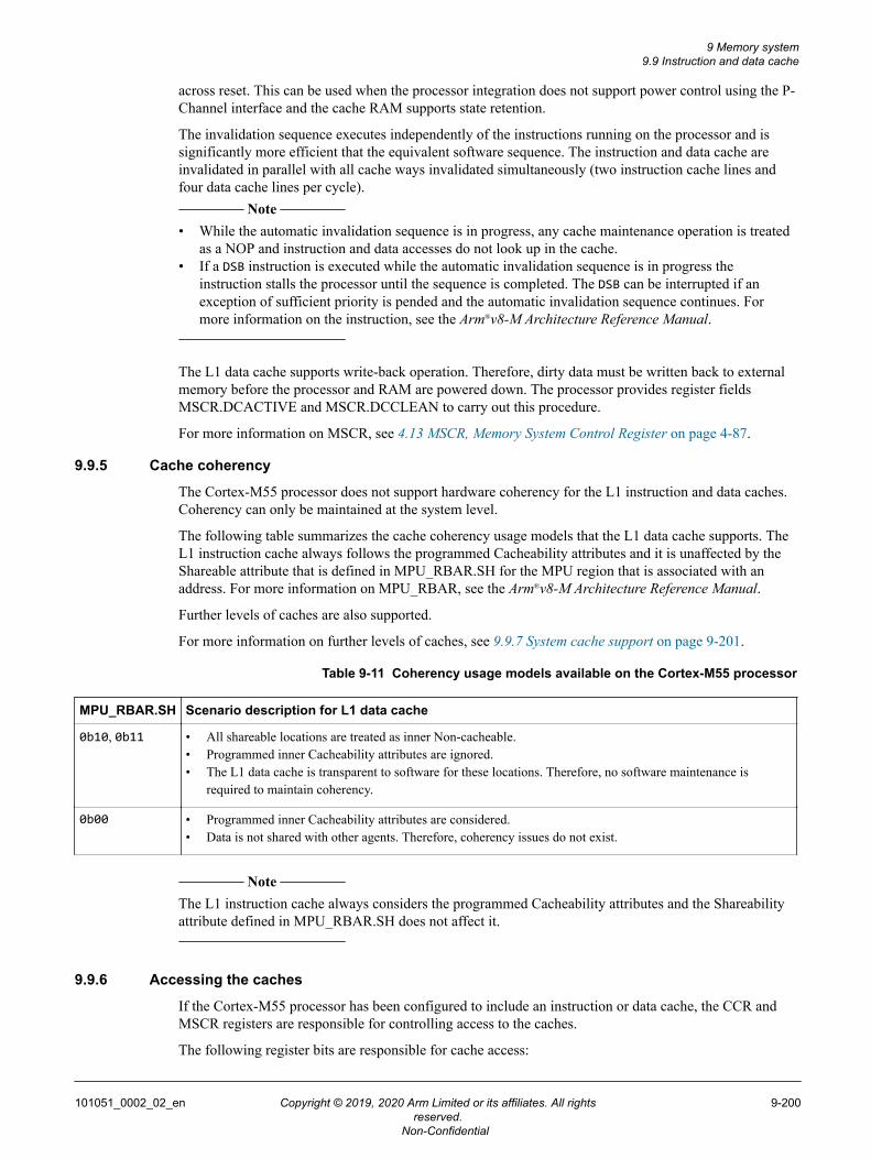
across reset. This can be used when the processor integration does not support power control using the P-Channel interface and the cache RAM supports state retention.
The invalidation sequence executes independently of the instructions running on the processor and issignificantly more efficient that the equivalent software sequence. The instruction and data cache areinvalidated in parallel with all cache ways invalidated simultaneously (two instruction cache lines andfour data cache lines per cycle).
Note
• While the automatic invalidation sequence is in progress, any cache maintenance operation is treatedas a NOP and instruction and data accesses do not look up in the cache.
• If a DSB instruction is executed while the automatic invalidation sequence is in progress theinstruction stalls the processor until the sequence is completed. The DSB can be interrupted if anexception of sufficient priority is pended and the automatic invalidation sequence continues. Formore information on the instruction, see the Arm®v8-M Architecture Reference Manual.
The L1 data cache supports write-back operation. Therefore, dirty data must be written back to externalmemory before the processor and RAM are powered down. The processor provides register fieldsMSCR.DCACTIVE and MSCR.DCCLEAN to carry out this procedure.
For more information on MSCR, see 4.13 MSCR, Memory System Control Register on page 4-87.
9.9.5 Cache coherency
The Cortex-M55 processor does not support hardware coherency for the L1 instruction and data caches.Coherency can only be maintained at the system level.
The following table summarizes the cache coherency usage models that the L1 data cache supports. TheL1 instruction cache always follows the programmed Cacheability attributes and it is unaffected by theShareable attribute that is defined in MPU_RBAR.SH for the MPU region that is associated with anaddress. For more information on MPU_RBAR, see the Arm®v8-M Architecture Reference Manual.
Further levels of caches are also supported.
For more information on further levels of caches, see 9.9.7 System cache support on page 9-201.
Table 9-11 Coherency usage models available on the Cortex-M55 processor
MPU_RBAR.SH Scenario description for L1 data cache
0b10, 0b11 • All shareable locations are treated as inner Non-cacheable.• Programmed inner Cacheability attributes are ignored.• The L1 data cache is transparent to software for these locations. Therefore, no software maintenance is
required to maintain coherency.
0b00 • Programmed inner Cacheability attributes are considered.• Data is not shared with other agents. Therefore, coherency issues do not exist.
Note
The L1 instruction cache always considers the programmed Cacheability attributes and the Shareabilityattribute defined in MPU_RBAR.SH does not affect it.
9.9.6 Accessing the caches
If the Cortex-M55 processor has been configured to include an instruction or data cache, the CCR andMSCR registers are responsible for controlling access to the caches.
The following register bits are responsible for cache access:
9 Memory system9.9 Instruction and data cache
101051_0002_02_en Copyright © 2019, 2020 Arm Limited or its affiliates. All rightsreserved.
9-200
Non-Confidential
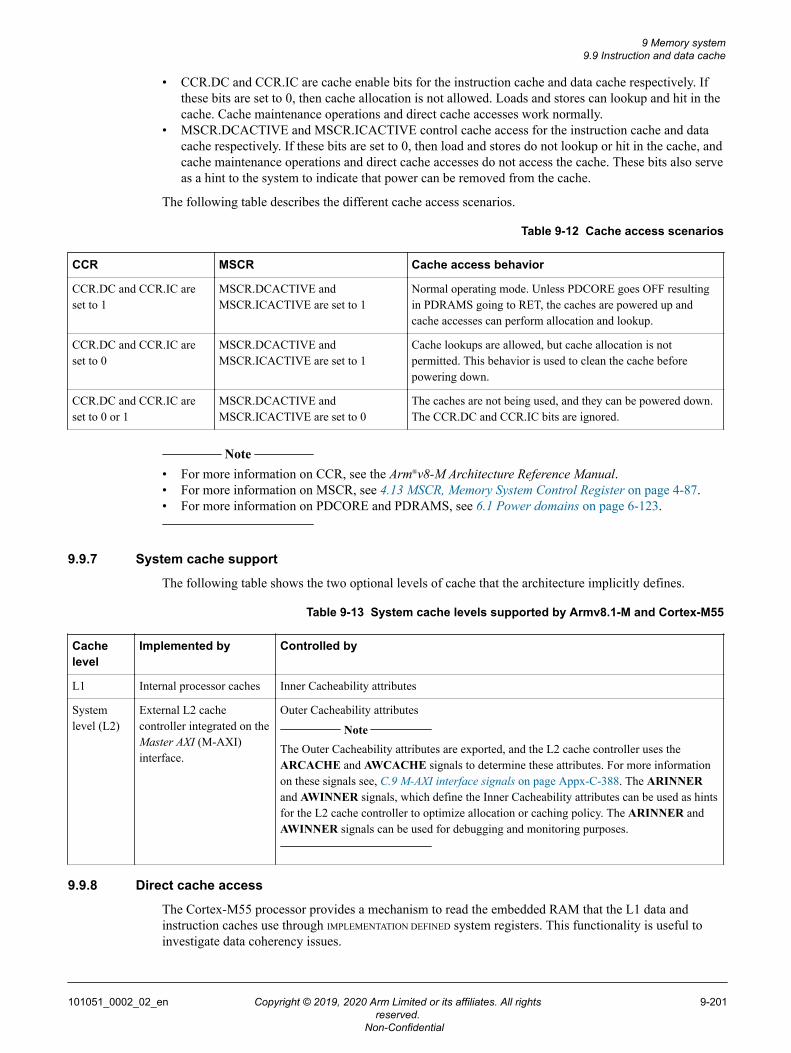
• CCR.DC and CCR.IC are cache enable bits for the instruction cache and data cache respectively. Ifthese bits are set to 0, then cache allocation is not allowed. Loads and stores can lookup and hit in thecache. Cache maintenance operations and direct cache accesses work normally.
• MSCR.DCACTIVE and MSCR.ICACTIVE control cache access for the instruction cache and datacache respectively. If these bits are set to 0, then load and stores do not lookup or hit in the cache, andcache maintenance operations and direct cache accesses do not access the cache. These bits also serveas a hint to the system to indicate that power can be removed from the cache.
The following table describes the different cache access scenarios.
Table 9-12 Cache access scenarios
CCR MSCR Cache access behavior
CCR.DC and CCR.IC areset to 1
MSCR.DCACTIVE andMSCR.ICACTIVE are set to 1
Normal operating mode. Unless PDCORE goes OFF resultingin PDRAMS going to RET, the caches are powered up andcache accesses can perform allocation and lookup.
CCR.DC and CCR.IC areset to 0
MSCR.DCACTIVE andMSCR.ICACTIVE are set to 1
Cache lookups are allowed, but cache allocation is notpermitted. This behavior is used to clean the cache beforepowering down.
CCR.DC and CCR.IC areset to 0 or 1
MSCR.DCACTIVE andMSCR.ICACTIVE are set to 0
The caches are not being used, and they can be powered down.The CCR.DC and CCR.IC bits are ignored.
Note
• For more information on CCR, see the Arm®v8-M Architecture Reference Manual.• For more information on MSCR, see 4.13 MSCR, Memory System Control Register on page 4-87.• For more information on PDCORE and PDRAMS, see 6.1 Power domains on page 6-123.
9.9.7 System cache support
The following table shows the two optional levels of cache that the architecture implicitly defines.
Table 9-13 System cache levels supported by Armv8.1-M and Cortex-M55
Cachelevel
Implemented by Controlled by
L1 Internal processor caches Inner Cacheability attributes
Systemlevel (L2)
External L2 cachecontroller integrated on theMaster AXI (M-AXI)interface.
Outer Cacheability attributes Note
The Outer Cacheability attributes are exported, and the L2 cache controller uses theARCACHE and AWCACHE signals to determine these attributes. For more informationon these signals see, C.9 M-AXI interface signals on page Appx-C-388. The ARINNERand AWINNER signals, which define the Inner Cacheability attributes can be used as hintsfor the L2 cache controller to optimize allocation or caching policy. The ARINNER andAWINNER signals can be used for debugging and monitoring purposes.
9.9.8 Direct cache access
The Cortex-M55 processor provides a mechanism to read the embedded RAM that the L1 data andinstruction caches use through IMPLEMENTATION DEFINED system registers. This functionality is useful toinvestigate data coherency issues.
9 Memory system9.9 Instruction and data cache
101051_0002_02_en Copyright © 2019, 2020 Arm Limited or its affiliates. All rightsreserved.
9-201
Non-Confidential
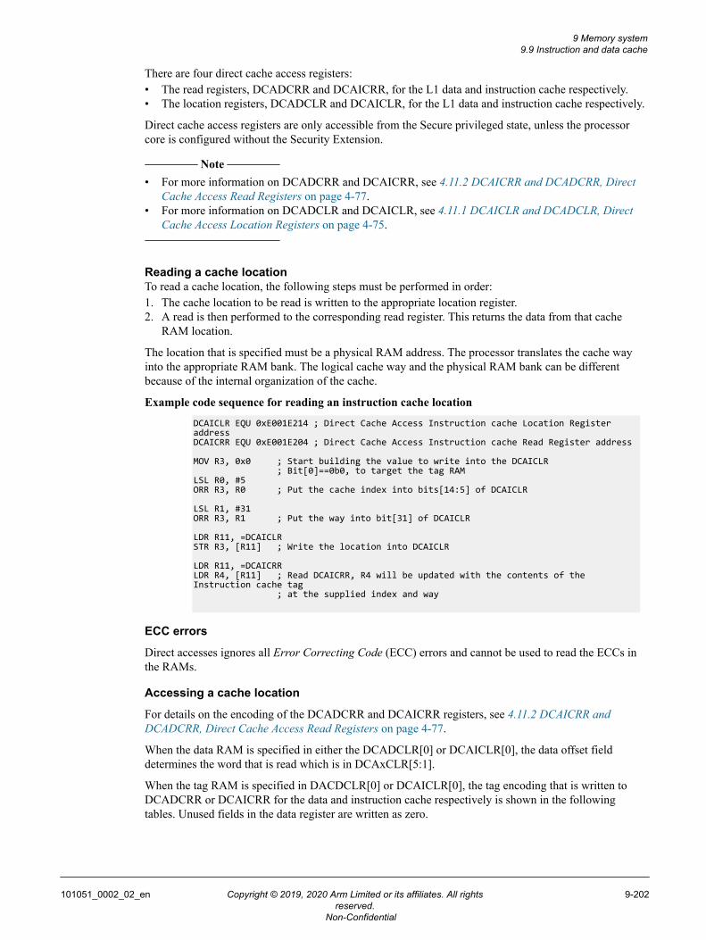
There are four direct cache access registers:• The read registers, DCADCRR and DCAICRR, for the L1 data and instruction cache respectively.• The location registers, DCADCLR and DCAICLR, for the L1 data and instruction cache respectively.
Direct cache access registers are only accessible from the Secure privileged state, unless the processorcore is configured without the Security Extension.
Note
• For more information on DCADCRR and DCAICRR, see 4.11.2 DCAICRR and DCADCRR, DirectCache Access Read Registers on page 4-77.
• For more information on DCADCLR and DCAICLR, see 4.11.1 DCAICLR and DCADCLR, DirectCache Access Location Registers on page 4-75.
Reading a cache locationTo read a cache location, the following steps must be performed in order:1. The cache location to be read is written to the appropriate location register.2. A read is then performed to the corresponding read register. This returns the data from that cache
RAM location.
The location that is specified must be a physical RAM address. The processor translates the cache wayinto the appropriate RAM bank. The logical cache way and the physical RAM bank can be differentbecause of the internal organization of the cache.
Example code sequence for reading an instruction cache location
DCAICLR EQU 0xE001E214 ; Direct Cache Access Instruction cache Location Register addressDCAICRR EQU 0xE001E204 ; Direct Cache Access Instruction cache Read Register address
MOV R3, 0x0 ; Start building the value to write into the DCAICLR ; Bit[0]==0b0, to target the tag RAMLSL R0, #5 ORR R3, R0 ; Put the cache index into bits[14:5] of DCAICLR
LSL R1, #31ORR R3, R1 ; Put the way into bit[31] of DCAICLR
LDR R11, =DCAICLRSTR R3, [R11] ; Write the location into DCAICLR
LDR R11, =DCAICRRLDR R4, [R11] ; Read DCAICRR, R4 will be updated with the contents of the Instruction cache tag ; at the supplied index and way
ECC errors
Direct accesses ignores all Error Correcting Code (ECC) errors and cannot be used to read the ECCs inthe RAMs.
Accessing a cache location
For details on the encoding of the DCADCRR and DCAICRR registers, see 4.11.2 DCAICRR andDCADCRR, Direct Cache Access Read Registers on page 4-77.
When the data RAM is specified in either the DCADCLR[0] or DCAICLR[0], the data offset fielddetermines the word that is read which is in DCAxCLR[5:1].
When the tag RAM is specified in DACDCLR[0] or DCAICLR[0], the tag encoding that is written toDCADCRR or DCAICRR for the data and instruction cache respectively is shown in the followingtables. Unused fields in the data register are written as zero.
9 Memory system9.9 Instruction and data cache
101051_0002_02_en Copyright © 2019, 2020 Arm Limited or its affiliates. All rightsreserved.
9-202
Non-Confidential
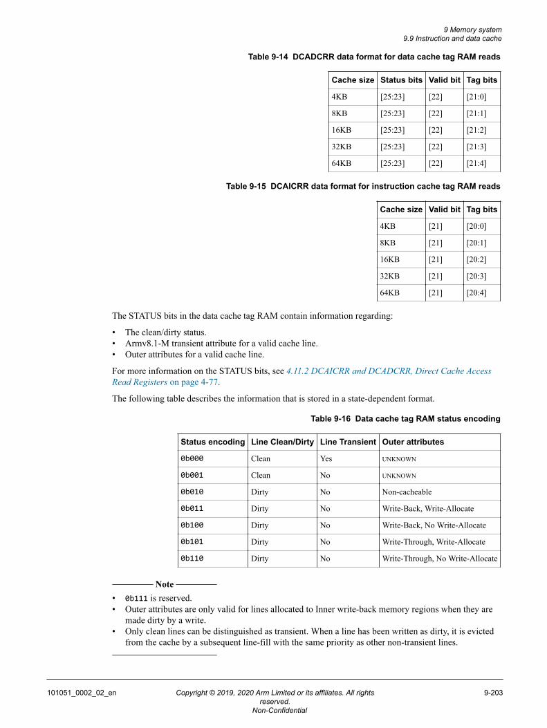
Table 9-14 DCADCRR data format for data cache tag RAM reads
Cache size Status bits Valid bit Tag bits
4KB [25:23] [22] [21:0]
8KB [25:23] [22] [21:1]
16KB [25:23] [22] [21:2]
32KB [25:23] [22] [21:3]
64KB [25:23] [22] [21:4]
Table 9-15 DCAICRR data format for instruction cache tag RAM reads
Cache size Valid bit Tag bits
4KB [21] [20:0]
8KB [21] [20:1]
16KB [21] [20:2]
32KB [21] [20:3]
64KB [21] [20:4]
The STATUS bits in the data cache tag RAM contain information regarding:
• The clean/dirty status.• Armv8.1‑M transient attribute for a valid cache line.• Outer attributes for a valid cache line.
For more information on the STATUS bits, see 4.11.2 DCAICRR and DCADCRR, Direct Cache AccessRead Registers on page 4-77.
The following table describes the information that is stored in a state-dependent format.
Table 9-16 Data cache tag RAM status encoding
Status encoding Line Clean/Dirty Line Transient Outer attributes
0b000 Clean Yes UNKNOWN
0b001 Clean No UNKNOWN
0b010 Dirty No Non-cacheable
0b011 Dirty No Write-Back, Write-Allocate
0b100 Dirty No Write-Back, No Write-Allocate
0b101 Dirty No Write-Through, Write-Allocate
0b110 Dirty No Write-Through, No Write-Allocate
Note
• 0b111 is reserved.• Outer attributes are only valid for lines allocated to Inner write-back memory regions when they are
made dirty by a write.• Only clean lines can be distinguished as transient. When a line has been written as dirty, it is evicted
from the cache by a subsequent line-fill with the same priority as other non-transient lines.
9 Memory system9.9 Instruction and data cache
101051_0002_02_en Copyright © 2019, 2020 Arm Limited or its affiliates. All rightsreserved.
9-203
Non-Confidential
9.10 Store bufferThe memory system includes a Store Buffer (STB) to hold data before it is written to the cache RAMs orpassed to the Master-AXI (M-AXI) interface. All store instructions to Normal memory regions that arenot the TCM, PPB, or Peripheral-AHB (P-AHB) interface must pass through the STB.
The STB has five identical slots which hold the address, up to 64 bits of data, and other attributes of storetransactions.
9.10.1 Store buffer merging
The Store Buffer (STB) has merging capabilities. If a previous write access has updated an entry, otherwrite accesses on the same doubleword can merge into this entry. Merging is only possible for stores toNormal memory.
Merging is not possible if:• The access is to Device memory.• The first access leaves the STB, either on the AXI or to the cache, before the second access reaches
the STB.• There is an attribute or security mismatch.• Either access is a Store-Exclusive.• The second access is a Store-Release.
9.10.2 Store buffer behavior
The Store Buffer (STB) directs cacheable write requests to the cache controller and Master-AXI (M-AXI)interface blocks.
Cache controller for cacheable write hitsThe store buffer sends a cache lookup to check that the cache hits in the specified line, and if so,the store buffer merges its data into the cache when the entry is drained.
M-AXI interfaceFor Non-cacheable, and Cacheable No Write-Allocate stores that miss in the L1 data cache, awrite access is performed on the M-AXI interface.For Cacheable Write-Allocate stores that miss in the data cache, a linefill is started using eitherof the two linefill buffers. The store data is sent to the linefill buffer first, and then the AXI datais merged.
9.10.3 Store buffer ordering
The Store Buffer (STB) has ordering capabilities and must maintain ordering between some stores.
The STB ordering is compulsory for the following stores:• All Device stores must occur in order with respect to other Device accesses.• Stores after a load-acquire must occur after the load-acquire.• Stores before a store-release must occur before the store-release.
9.10.4 Store buffer draining
The Store Buffer (STB) is drained of all stores to Device memory before a load is performed from Devicememory.
Slots that are Non-mergeable drain quickly because there is no benefit in being present in the STB.Mergeable slots might wait for future stores to merge into them and reduce the number of cache writesrequired.
A store buffer entry is drained if:• There is a cache maintenance operation pending.• There is a store that cannot enter the STB because of the current contents of the STB.
9 Memory system9.10 Store buffer
101051_0002_02_en Copyright © 2019, 2020 Arm Limited or its affiliates. All rightsreserved.
9-204
Non-Confidential
• There is a DSB, DMB, ESB, WFI, or WFE instruction.• There are debug events.
9 Memory system9.10 Store buffer
101051_0002_02_en Copyright © 2019, 2020 Arm Limited or its affiliates. All rightsreserved.
9-205
Non-Confidential
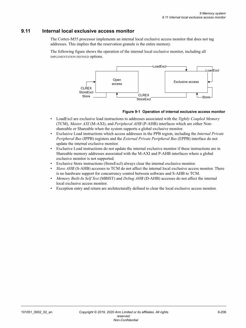
9.11 Internal local exclusive access monitorThe Cortex-M55 processor implements an internal local exclusive access monitor that does not tagaddresses. This implies that the reservation granule is the entire memory.
The following figure shows the operation of the internal local exclusive monitor, including allIMPLEMENTATION DEFINED options.
Exclusive accessOpen access
LoadExclLoadExcl
StoreCLREXStoreExcl
CLREXStoreExcl
Store
Figure 9-1 Operation of internal exclusive access monitor
• LoadExcl are exclusive load instructions to addresses associated with the Tightly Coupled Memory(TCM), Master AXI (M-AXI), and Peripheral AHB (P-AHB) interfaces which are either Non-shareable or Shareable when the system supports a global exclusive monitor.
• Exclusive Load instructions which access addresses in the PPB region, including the Internal PrivatePeripheral Bus (IPPB) registers and the External Private Peripheral Bus (EPPB) interface do notupdate the internal exclusive monitor.
• Exclusive Load instructions do not update the internal exclusive monitor if these instructions are inShareable memory addresses associated with the M-AXI and P-AHB interfaces where a globalexclusive monitor is not supported.
• Exclusive Store instructions (StoreExcl) always clear the internal exclusive monitor.• Slave AHB (S-AHB) accesses to TCM do not affect the internal local exclusive access monitor. There
is no hardware support for concurrency control between software and S-AHB to TCM.• Memory Built-In Self Test (MBIST) and Debug AHB (D-AHB) accesses do not affect the internal
local exclusive access monitor.• Exception entry and return are architecturally defined to clear the local exclusive access monitor.
9 Memory system9.11 Internal local exclusive access monitor
101051_0002_02_en Copyright © 2019, 2020 Arm Limited or its affiliates. All rightsreserved.
9-206
Non-Confidential
9.12 M-AXI and P-AHB interaction with the global exclusive monitorThe Master AXI (M-AXI) and Peripheral AHB (P-AHB) interfaces support systems that include a globalexclusive monitor by using the interface signals that conform to the AMBA 5 AXI and AMBA 5 AHBprotocols respectively.
Accesses associated with load and store exclusive instructions are only handled as exclusive on the M-AXI and P-AHB interfaces if they are either of the following:
• Device memory.• Normal memory marked as Shareable in the associated Memory Protection Unit (MPU) region.
Exclusive accesses to Normal Shareable memory are always treated as Shareable Non-cacheable by theprocessor.
Only the internal exclusive access monitor handles accesses to Non-shareable memory.
If an Exclusive read access is carried out to a region that does not support a global exclusive monitor, theslave must respond in either of the following ways:• An OKAY response for AXI.• The HEXOKAYP response must be deasserted for P-AHB.
These responses do not result in the processor taking an exception, but they do ensure that the STREXdoes not pass. This kind of livelock behavior can be trapped using a Watchdog unit.
Note
The default memory map includes only Non-shareable Normal memory regions. Therefore, Cortex-M55processor configurations without an MPU can only generate external exclusive load and store operationsfrom Device memory in either the Peripheral region, External Device region or Vendor_SYS region. Formore information on the memory map, see 7.1 Memory map on page 7-144
9 Memory system9.12 M-AXI and P-AHB interaction with the global exclusive monitor
101051_0002_02_en Copyright © 2019, 2020 Arm Limited or its affiliates. All rightsreserved.
9-207
Non-Confidential
9.13 MBISTThe Cortex-M55 processor supports the production Memory Built-In Self-Test (MBIST) use model.
This allows memory testing during manufacture. This use model requires that a production MBISTcontroller is inserted into the processor and connected to the internal MBIST interface. This can beautomatically carried out by EDA tools using configuration information that is delivered with theprocessor.
Note
The Cortex-M55 processor does not support an external MBIST interface.
9 Memory system9.13 MBIST
101051_0002_02_en Copyright © 2019, 2020 Arm Limited or its affiliates. All rightsreserved.
9-208
Non-Confidential
Chapter 10Reliability, Availability, and Serviceability Extensionsupport
This chapter describes the Reliability, Availability, and Serviceability (RAS) features implemented in theCortex-M55 processor.
It contains the following sections:• 10.1 Cortex®-M55 processor implementation of RAS on page 10-210.• 10.2 ECC memory protection behavior on page 10-212.• 10.3 Interface protection behavior on page 10-219.• 10.4 RAS memory barriers on page 10-221.• 10.5 RAS Extension registers on page 10-222.
101051_0002_02_en Copyright © 2019, 2020 Arm Limited or its affiliates. All rightsreserved.
10-209
Non-Confidential
10.1 Cortex®-M55 processor implementation of RASThe Cortex-M55 processor implements the Reliability, Availability, and Serviceability (RAS) features toensure correct operation in environments where functional safety and high-availability are critical. TheRAS Extension is always included in the Cortex-M55 processor, however most of the features are onlysupported when Error Correcting Code (ECC) is configured and enabled.
The Cortex-M55 processor standardizes the software interface for fault detection and analysis bysupporting the RAS Extension. The RAS features supported are Error Correcting Code (ECC) for the L1instruction cache and data cache, and TCMs.
Errors are reported to the system through:• Output signals on the processor. For more information, see C.28 Error interface signals
on page Appx-C-417• Error bank registers which can be used to mitigate hard errors that cannot be corrected by writing
back to the RAM. For more information, see 4.12 Error bank registers on page 4-81.• The architectural registers that are defined by the RAS Extension. For more information, see
10.5 RAS Extension registers on page 10-222
Supported RAS architectural featuresThe RAS architecture contains:• An Error Synchronization Barrier (ESB) instruction.• An implicit ESB operation that is inserted after exception entry, exception return, and lazy stacking.
This feature is enabled by setting AIRCR.IESB. For more information on AIRCR, see the Arm®v8-MArchitecture Reference Manual.
• Two ID registers, ERRDEVID and ID_PFR0. For more information on these registers, see theArm®v8-M Architecture Reference Manual.
• A fault status register, RFSR, that is dedicated to RAS events. For more information on:— RAS events, see 10.1.1 Cortex®-M55 RAS events on page 10-210.— RFSR, see 10.5.7 RFSR, RAS Fault Status Register on page 10-229.
• A summary register indicating the nodes that have detected RAS events, ERRGSR. For moreinformation on this register, see 10.5.5 ERRGSR0, RAS Fault Group Status Register on page 10-228.A node is a unit that can detect RAS events, and for Cortex-M55, a node is the entire processor.Therefore, all RAS events are logged in the same location and the processor supports a single errorrecord.
• Each node has one set of Error Record Registers that can store information about the last RAS eventthat the node has detected.
The RAS Error Record Registers are independent of the Error Bank Registers, although they havesome common behavior. Either or both of the register types can be used by system software that ishandling errors. However, for compatibility across other devices and systems that implement the RASExtension, the RAS programmers' model must be considered. The RAS Error Record Registers aredescribed in 10.5 RAS Extension registers on page 10-222 and the Error Bank Registers are describedin 4.12 Error bank registers on page 4-81.
Tip
For a complete description of RAS error types and the information on RAS errors that areproduced at the node, see the Arm® Reliability, Availability, and Serviceability (RAS) Specification.
This section contains the following subsection:• 10.1.1 Cortex®-M55 RAS events on page 10-210.
10.1.1 Cortex®-M55 RAS events
The Reliability, Availability, and Serviceability (RAS) Extension provides a standard model for recordingand reporting errors which might occur during the operation of a system.
10 Reliability, Availability, and Serviceability Extension support10.1 Cortex®-M55 processor implementation of RAS
101051_0002_02_en Copyright © 2019, 2020 Arm Limited or its affiliates. All rightsreserved.
10-210
Non-Confidential
In the Cortex-M55 processor, the following are considered as RAS events:• L1 instruction cache Error Correcting Code (ECC) errors.• L1 data cache ECC errors.• TCM ECC errors.
Note
For more information on how these RAS events are detected and handled in the Cortex-M55 processor,see 10.2 ECC memory protection behavior on page 10-212 to get an overview on how instruction cache,data cache, and TCM ECC errors are handled.
10 Reliability, Availability, and Serviceability Extension support10.1 Cortex®-M55 processor implementation of RAS
101051_0002_02_en Copyright © 2019, 2020 Arm Limited or its affiliates. All rightsreserved.
10-211
Non-Confidential
10.2 ECC memory protection behaviorError Correcting Code (ECC) memory protection is optional. At implementation, you can configure theCortex-M55 processor to include ECC or not using the Verilog parameter, ECC. At Cold reset, if theCortex-M55 processor is configured with ECC, you can control whether ECC is enabled or not using thestatic configuration signal INITECCEN. INITECCEN must only be changed when the processor ispowered down and in Cold or Warm reset.
ECC memory protection includes the following protection features:• Data protection• Address decoder protection, which involves detecting some of the errors that might occur because of
a failure in the address decoder in a RAM instance• White noise protection, which involves protection against faults in the RAM that might also result in
no entry being selected and therefore, resulting in reading either all zeros or all ones
Note
In the case when a fault in a RAM address decoder circuit results in the wrong RAM entry being selected(typically contains data and ECC that are self-consistent), address decoder protection is not supportedand an ECC error is not generated. In this case, the wrong data is read from the RAM.
10.2.1 ECC schemes and error type terminology
The Cortex-M55 processor supports two Error Correcting Code (ECC) schemes to detect errors.
ECC schemes
SECDEDSingle Error Correct Double Error Detect (SECDED) is used on the L1 data cache and TCMRAMs. The SECDED scheme also provides information on how to correct the error.
DEDDouble Error Detect (DED) is used on the L1 instruction cache RAMs. The DED schemedetects single bit and double bit errors. The instruction cache does not need a correctionmechanism or scheme because the contents must always be consistent with external memory.Therefore, you can always invalidate the instruction cache RAM to correct its contents.
In the Cortex-M55 processor, the ECC schemes can also support detection of some multi-bit errors wheremore than two bits are incorrect. Where possible, RAM location information is included in the ECC codeto allow fault detection in the RAM decoder logic.
Error type terminology
The following error type terminology is used in this manual in the context of ECC:
Single-bit errorAn error where only one bit of the data or ECC code is incorrect. These errors can usually becorrected.
Note
If an error bit is located in an ECC code field that is associated with the RAM location, thisindicates that the read has been carried out from the wrong address in the block. These errors aremulti-bit errors because the incorrect line has been read and all of the data is wrong.
Multi-bit errorAn error in which more than one bit of data or ECC code is incorrect, or a single-bit error isreported in an ECC code field that is associated with the RAM location.
10 Reliability, Availability, and Serviceability Extension support10.2 ECC memory protection behavior
101051_0002_02_en Copyright © 2019, 2020 Arm Limited or its affiliates. All rightsreserved.
10-212
Non-Confidential
Corrected error (CE)An ECC error that is detected by hardware and that hardware can correct. These are:• Single bit errors, which can be corrected inline by flipping the faulty bit.• All errors which can be corrected by refetching the data from external memory. This
includes all instruction cache errors and all data cache errors when the cache line can beguaranteed to be clean.
For more information on Corrected errors (CEs), see Arm® Reliability, Availability, andServiceability (RAS) Specification.
Uncorrected error (UE)An ECC error that cannot be corrected or deferred. These are multi-bit errors:• From the TCMs.• In an L1 dirty data cache data RAM where it is not guaranteed that the cache line is clean.
This includes the case where the ECC indicates that the RAM location is incorrect.• In an L1 dirty data cache tag RAM where it is not guaranteed that the cache is clean. This
includes the case where the ECC indicates that the RAM location is incorrect.
For more information on Uncorrected errors (UEs), see Arm® Reliability, Availability, andServiceability (RAS) Specification.
10.2.2 Enabling ECC
If configured in the processor, Error Correcting Code (ECC) is enabled at reset using the input signalINITECCEN.
For more information on INITECCEN, see C.4 Reset configuration signals on page Appx-C-381. Formore information on MSCR, see 4.13 MSCR, Memory System Control Register on page 4-87.
If ECC is enabled out of reset, the L1 cache must be invalidated before it is enabled to avoid spuriousECC errors being detected because of a mismatch between the data and ECC in the RAM. Automaticinstruction and data cache invalidation can be enabled at reset by tying the input signal INITL1RSTDISLOW. For more information on INITL1RSTDIS, see C.4 Reset configuration signalson page Appx-C-381. For more information on automatic cache invalidation, see 9.9.4 Automatic cacheinvalidation at reset on page 9-199 .
Note
Software can determine whether ECC is configured and enabled by reading MSCR.ECCEN. However,software cannot enable ECC.
10.2.3 Error detection and processing
The Cortex-M55 processor core is responsible for error detection and processing. Multiple errors canoccur simultaneously, therefore, the processor prioritizes the error processing based on the source.
The following figure shows the prioritization of error processing that occurs in the order of decreasingpriority.
10 Reliability, Availability, and Serviceability Extension support10.2 ECC memory protection behavior
101051_0002_02_en Copyright © 2019, 2020 Arm Limited or its affiliates. All rightsreserved.
10-213
Non-Confidential
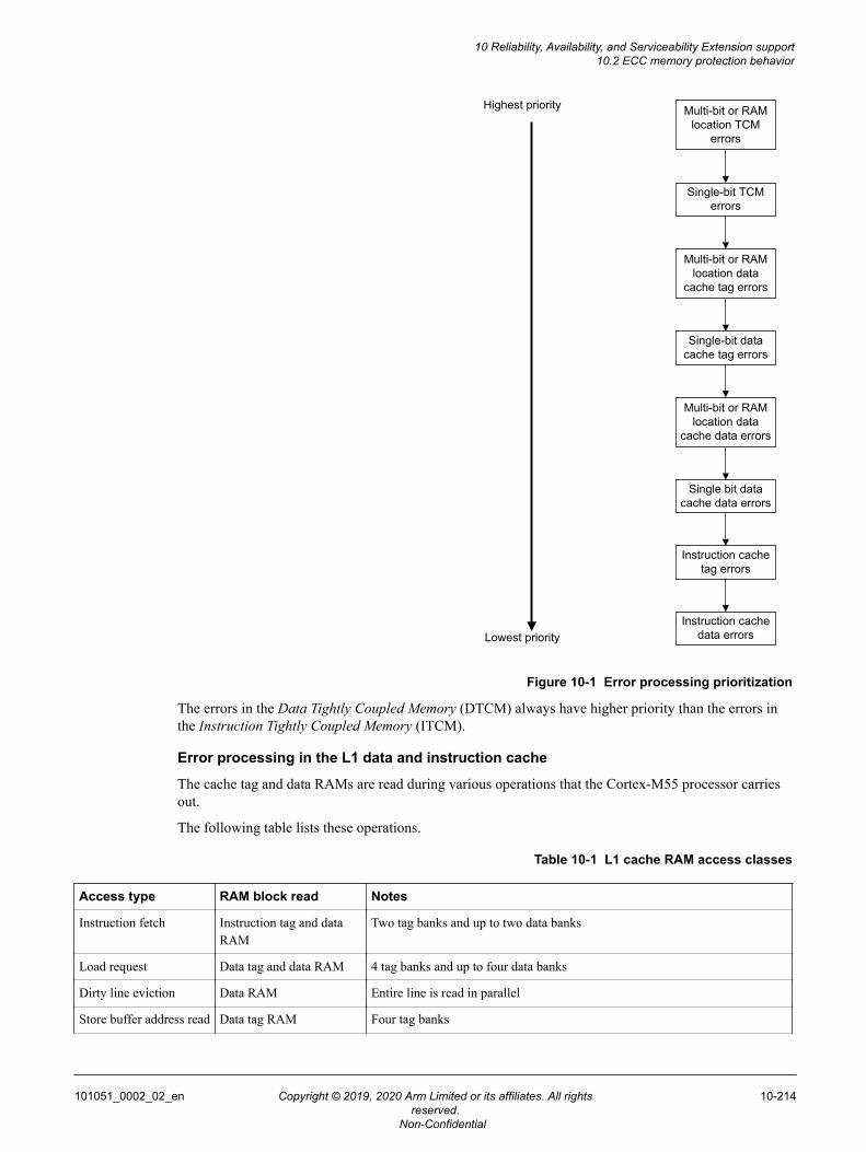
Multi-bit or RAM location TCM
errors
Single-bit TCM errors
Multi-bit or RAM location data
cache tag errors
Single-bit data cache tag errors
Multi-bit or RAM location data
cache data errors
Single bit data cache data errors
Instruction cache tag errors
Instruction cache data errors
Highest priority
Lowest priority
Figure 10-1 Error processing prioritization
The errors in the Data Tightly Coupled Memory (DTCM) always have higher priority than the errors inthe Instruction Tightly Coupled Memory (ITCM).
Error processing in the L1 data and instruction cache
The cache tag and data RAMs are read during various operations that the Cortex-M55 processor carriesout.
The following table lists these operations.
Table 10-1 L1 cache RAM access classes
Access type RAM block read Notes
Instruction fetch Instruction tag and dataRAM
Two tag banks and up to two data banks
Load request Data tag and data RAM 4 tag banks and up to four data banks
Dirty line eviction Data RAM Entire line is read in parallel
Store buffer address read Data tag RAM Four tag banks
10 Reliability, Availability, and Serviceability Extension support10.2 ECC memory protection behavior
101051_0002_02_en Copyright © 2019, 2020 Arm Limited or its affiliates. All rightsreserved.
10-214
Non-Confidential
Table 10-1 L1 cache RAM access classes (continued)
Access type RAM block read Notes
Store buffer data read Data data RAM Only used for Read-Modify-Write (RMW). RMW is used when the processorwrites a partial word when ECC is enabled. Store operations to a cache line,which are less that 64 bits of data must read the data RAM to construct theECC to write back. This is based on the combination of the current and newdata. This read operation can result in an error being detected in the data RAM.
Data cache maintenance Tag RAM and data RAM Tag RAM read for address-based and clean operations.
Data RAM read for clean evictions.
The error processing operations are:
Instruction fetchAll Error Correcting Code (ECC) errors on instruction fetches are processed by invalidating thetag RAM and refetching the line from external memory.
Corrected errors in the L1 data cache for load and store operationsCorrected errors (CE) in the L1 data cache that are detected on load, store, and cachemaintenance operations are processed by cleaning (if required) and invalidating the location.For load operations, the data is corrected by replaying, which is refetching and executing theinstruction, causing a data cache miss on the invalidated location and reading the correct datafrom external memory.Store operations to Write-Allocate memory request a linefill after the error has been processedand then merge the write data into the line as it is allocated to the cache. Store operations to aline in the cache which write less than 64 bits of data must read the data RAM to construct theECC to write-back, based on a combination of the current and new data. This read operation canresult in an error being detected in the data RAM.
Cache maintenance operations
Data cache maintenance operations which operate on an address read all four tag RAMs tocheck for a match. Instruction cache maintenance operations which operate on an address readtwo tag RAMs to check for a match. Therefore, they can potentially detect multiple errorsunrelated to the requested location. The operation automatically cleans and invalidates alldetected errors in sequence. Cache maintenance invalidate by set/way location carried out byNon-secure code always reads the tag because it might contain a dirty line associated with aSecure address, and therefore, it must be cleaned to prevent data loss before being invalidated.The behavior of cache maintenance operations in Non-secure state is described in 9.9.3 Cachemaintenance operations on page 9-198.
Dirty line evictionIn all cases where a line is evicted, the data RAM associated with the entire line is read out ofthe cache. Any error detected in this read is corrected inline before being written back to theexternal memory through the Master AXI (M-AXI) interface. If a multi-bit error is detected inthe data, the line is marked as poisoned and an imprecise BusFault is raised ifMSCR.EVECCFAULT is set.
Multiple errors are processed according to the priority listed in 10.2.3 Error detection and processingon page 10-213 . Errors during load operations are handled by replaying the instruction, therefore, it ispossible for errors found in multiple cache ways to not be processed if the original lookup is notrepeated. For example, if the replayed load is interrupted.
10 Reliability, Availability, and Serviceability Extension support10.2 ECC memory protection behavior
101051_0002_02_en Copyright © 2019, 2020 Arm Limited or its affiliates. All rightsreserved.
10-215
Non-Confidential
If data is lost because of a multi-bit ECC error, then an Imprecise BusFault is generated under thefollowing conditions:• If a data cache eviction is performed, and a multi-bit error is detected in the data RAM and
MSCR.EVECCFAULT is set.• If a data cache line is invalidated because of a multi-bit error detected in the Tag RAM, and
MSCR.DCCLEAN is not set.
Although loads do not directly cause BusFaults, they cause ECC maintenance behavior that triggers aBusFault if data is lost. Additionally, if any load sees an ECC error the pipe is flushed, and the loadcannot progress until the ECC maintenance has finished. This guarantees that the core does not consumeerroneous data until an Imprecise BusFault has been generated.
A multi-bit error on the data cache tag when MSCR.DCCLEAN is asserted is always correctable as thecorresponding cache line cannot contain any dirty data.
A multi-bit error on the data cache data when MSCR.EVECCFAULT is deasserted is consideredDeferred (DE), because when that line is evicted, it is marked as poisoned. MSCR.EVECCFAULT beingdeasserted implies that the system supports poisoning.
Any other case of multi-bit errors in the data cache is considered Uncorrected.
Error processing in the TCMs
Error detection and correction are carried out on each of the individual TCMS, that is, ITCM, D0TCM,D1TCM, D2TCM, and D3TCM. Accesses to each of the interfaces are treated in the following way:
• Correctable errors detected during instruction fetch and load operations result in the read beingrepeated either by refetching the instruction address or replaying the load instruction. The correcteddata is written back to the TCM.
• Correctable errors from read requests on the Slave AHB (S-AHB) are corrected inline and returned tothe system on completion of the transaction.
• Write requests to the TCM with an access size smaller than a complete word or with non-contiguousbytes from S-AHB or M‑profile Vector Extension (MVE) operations must carry out a Read-Modify-Write (RMW) sequence to the TCM. Correctable errors detected during the sequence are correctedinline before the complete store word is written back to the TCM. Uncorrectable errors that aredetected on the read phase of an RMW sequence cause the write phase to be abandoned, and theaddress is marked as poisoned in the error bank register. If the location is read again, a preciseBusFault is raised.
• When ECC is enabled, an instruction fetch or load operations might raise a precise BusFaultexception, if an Uncorrected error (UE) is detected.
Note
When ECC is enabled, before performing a byte, halfword, or unaligned word write to a TCM locationwhich causes an RMW, you must initialize the location first by performing an aligned word ordoubleword write to the location. Arm recommends that all TCM locations are initialized in this mannerby boot code.
10.2.4 Error reporting
Error reporting is done using both registers and output signals.
Corrected errors
Corrected errors (CE) are always transparent to program flow. For more information on Corrected errors(CEs), see Arm® Reliability, Availability, and Serviceability (RAS) Specification.
Uncorrected errors
Uncorrected errors (UEs) can result in a precise or imprecise BusFault. If an exception occurs, the sourceof the error can be determined using the AFSR and RFSR.
10 Reliability, Availability, and Serviceability Extension support10.2 ECC memory protection behavior
101051_0002_02_en Copyright © 2019, 2020 Arm Limited or its affiliates. All rightsreserved.
10-216
Non-Confidential
An imprecise BusFault is raised when a UE is found in the data cache data RAM during an eviction. Ifthe system supports poisoning, clearing MSCR.EVECCFAULT disables this error. An impreciseBusFault is also raised when a UE is found in the data cache tag RAM and MCSR.DCCLEAN is not setand this type of BusFault cannot be disabled. For more information on Uncorrected errors (UEs), seeArm® Reliability, Availability, and Serviceability (RAS) Specification.
Errors detected on accesses to the TCMs never result in an imprecise BusFault.
Errors on the L1 instruction cache, L1 data cache, and TCMs
Errors detected in the L1 instruction cache, L1 data cache, and TCMs are reported on the followingexternal error interface output signals:
• DMEV0• DMEV1• DMEV2• DMEL0[2:0]• DMEL1[2:0]• DMEI0[25:0]• DMEI1[25:0]
Up to two errors can be reported on the same cycle. If multiple simultaneous errors occur, the priorityscheme for reporting is followed. The reporting priority is described in 10.2.3 Error detection andprocessing on page 10-213. If up to two errors occur, the location and error class is indicated in DMELnand DMEIn respectively, and DMEVn is asserted. If more than two errors occur, then only informationabout the two highest priority errors are reported and DMEV2 is asserted to indicate further informationis not available.
For more information on the error interface signals, see C.28 Error interface signalson page Appx-C-417
Note
A particular ECC error might be reported multiple times on the DME bus.
Error bank registers
The processor includes internal error bank registers which do the following:
• Record the two most recent errors detected.• Isolate the system from hard errors in the RAM which cannot be corrected by invalidating or
overwriting with correct data.
Two error bank registers are included for each source of errors:• IEBR0 and IEBR1 for the L1 instruction cache.• DEBR0 and DEBR1 for the L1 data cache.• TEBR0, TEBR1, TEBRDATA0, and TEBRDATA1 that are shared across the ITCM and DTCM.
Error bank behavior
When an error bank contains a valid entry, any errors detected from the associated RAM address areignored.
L1 instruction and data cache
For the L1 instruction and data cache, the RAM addresses are masked on a cache lookup and nolonger used for allocating a line on a miss, isolating the processor from any potential hard errorsin the RAM which could cause incorrect behavior even if corrected data is written from externalmemory.
10 Reliability, Availability, and Serviceability Extension support10.2 ECC memory protection behavior
101051_0002_02_en Copyright © 2019, 2020 Arm Limited or its affiliates. All rightsreserved.
10-217
Non-Confidential
TCMs
For TCMs, each TCM error bank contains a 32-bit data register TEBRDATAn. When a single-bit TCM fault is detected and the error bank is allocated, the corrected data is written to the dataregister and the TCM memory. Any subsequent read returns the result directly fromTEBRDATAn. Writes to an address associated with a valid TCM Error bank is written to boththe TEBRDATAn and the TCM RAM to maintain consistency if the error bank is reallocated orcleared by software. If a multi-bit error is detected on a read from the TCM RAM, the errorbank TEBRn.POISON field is set. When this field has been set any subsequent read requests tothe TCM which matches the error bank address, it will result in an error. A precise BusFault willbe raised for a load request from the processor and HRESP is asserted on a read on the SlaveAHB (S-AHB) interface.
Write accesses from store instructions or S-AHB to TCM that match an error bank register withTEBRn.POISON set do not raise a fault. The TEBRn.POISON field is cleared by an aligned 32-bit write to the address associated with the TCM error bank register. The behavior of the poisonfeature in the TCM error bank register allows hard multi-bit errors to be patched by software.For example:1. Load from the TCM at an address detects a multi-bit Error Correcting Code (ECC) error.
TEBRn is allocated, TEBRn.POISON is set, and a fault is raised.2. Patch write data of 32 bits is stored to the TCM at that address. TEBRDATAn and TCM
memory are updated and TEBRn.POISON is cleared.3. Subsequent read and write transactions to that address are completed as expected.
If this sequence is applied, the failing TCM RAM entry is isolated and normal execution cancontinue when the write is applied, even when the error is Hard and so cannot be cleared by apatch directly to the RAM. Between steps 1 and 2, read and write transactions with size lessthan a word continue to raise a fault because the address has not been patched.
The error bank registers are updated when an ECC error from the associated RAM controller has beenprocessed and remains valid until either a subsequent error is detected and processed, or a direct softwarewrite to the bank is carried out to clear the data.
Invalid error banks are always allocated in preference to valid error banks. If both error banks containvalid data new errors are allocated using a round-robin approach. Error banks can be locked from beingoverwritten by writing to the LOCKED field in the error bank register.
The error bank registers are only cleared on Cold reset and retain their content on system reset.
10.2.5 Address decoder protection and white noise protection
The Cortex-M55 processor includes address decoder protection and white noise protection.
Address decoder protectionAddress decoder protection detects some of the errors that might occur because of a failure inthe address decoder in a RAM instance. A fault in a RAM address decoder circuit might resultin the wrong RAM entry being selected, which typically contains data and ECC that are self-consistent. Therefore, an ECC error on the data is not generated in this case, but the wrong datais read from the RAM.
White noise protectionA fault in a RAM might result in no entry being selected, which might result in reading either allzeros or all ones. Protection against such faults is white noise protection.
10 Reliability, Availability, and Serviceability Extension support10.2 ECC memory protection behavior
101051_0002_02_en Copyright © 2019, 2020 Arm Limited or its affiliates. All rightsreserved.
10-218
Non-Confidential
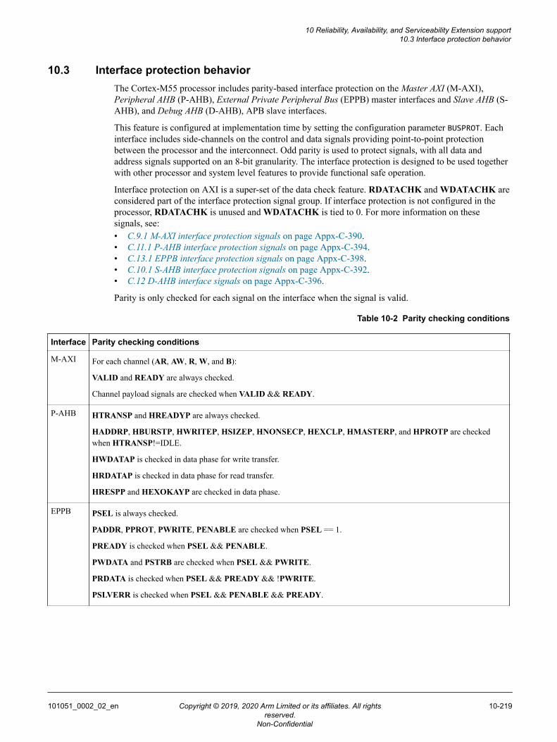
10.3 Interface protection behaviorThe Cortex-M55 processor includes parity-based interface protection on the Master AXI (M-AXI),Peripheral AHB (P-AHB), External Private Peripheral Bus (EPPB) master interfaces and Slave AHB (S-AHB), and Debug AHB (D-AHB), APB slave interfaces.
This feature is configured at implementation time by setting the configuration parameter BUSPROT. Eachinterface includes side-channels on the control and data signals providing point-to-point protectionbetween the processor and the interconnect. Odd parity is used to protect signals, with all data andaddress signals supported on an 8-bit granularity. The interface protection is designed to be used togetherwith other processor and system level features to provide functional safe operation.
Interface protection on AXI is a super-set of the data check feature. RDATACHK and WDATACHK areconsidered part of the interface protection signal group. If interface protection is not configured in theprocessor, RDATACHK is unused and WDATACHK is tied to 0. For more information on thesesignals, see:• C.9.1 M-AXI interface protection signals on page Appx-C-390.• C.11.1 P-AHB interface protection signals on page Appx-C-394.• C.13.1 EPPB interface protection signals on page Appx-C-398.• C.10.1 S-AHB interface protection signals on page Appx-C-392.• C.12 D-AHB interface signals on page Appx-C-396.
Parity is only checked for each signal on the interface when the signal is valid.
Table 10-2 Parity checking conditions
Interface Parity checking conditions
M-AXI For each channel (AR, AW, R, W, and B):
VALID and READY are always checked.
Channel payload signals are checked when VALID && READY.
P-AHB HTRANSP and HREADYP are always checked.
HADDRP, HBURSTP, HWRITEP, HSIZEP, HNONSECP, HEXCLP, HMASTERP, and HPROTP are checkedwhen HTRANSP!=IDLE.
HWDATAP is checked in data phase for write transfer.
HRDATAP is checked in data phase for read transfer.
HRESPP and HEXOKAYP are checked in data phase.
EPPB PSEL is always checked.
PADDR, PPROT, PWRITE, PENABLE are checked when PSEL == 1.
PREADY is checked when PSEL && PENABLE.
PWDATA and PSTRB are checked when PSEL && PWRITE.
PRDATA is checked when PSEL && PREADY && !PWRITE.
PSLVERR is checked when PSEL && PENABLE && PREADY.
10 Reliability, Availability, and Serviceability Extension support10.3 Interface protection behavior
101051_0002_02_en Copyright © 2019, 2020 Arm Limited or its affiliates. All rightsreserved.
10-219
Non-Confidential
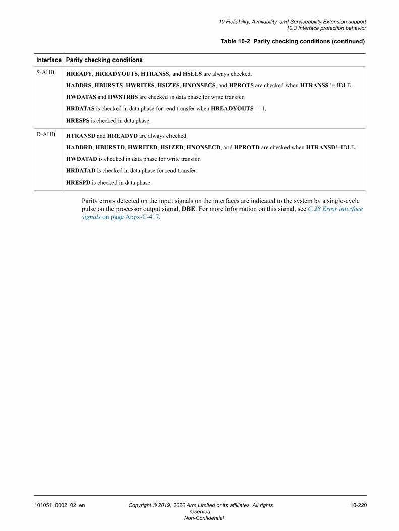
Table 10-2 Parity checking conditions (continued)
Interface Parity checking conditions
S-AHB HREADY, HREADYOUTS, HTRANSS, and HSELS are always checked.
HADDRS, HBURSTS, HWRITES, HSIZES, HNONSECS, and HPROTS are checked when HTRANSS != IDLE.
HWDATAS and HWSTRBS are checked in data phase for write transfer.
HRDATAS is checked in data phase for read transfer when HREADYOUTS ==1.
HRESPS is checked in data phase.
D-AHB HTRANSD and HREADYD are always checked.
HADDRD, HBURSTD, HWRITED, HSIZED, HNONSECD, and HPROTD are checked when HTRANSD!=IDLE.
HWDATAD is checked in data phase for write transfer.
HRDATAD is checked in data phase for read transfer.
HRESPD is checked in data phase.
Parity errors detected on the input signals on the interfaces are indicated to the system by a single-cyclepulse on the processor output signal, DBE. For more information on this signal, see C.28 Error interfacesignals on page Appx-C-417.
10 Reliability, Availability, and Serviceability Extension support10.3 Interface protection behavior
101051_0002_02_en Copyright © 2019, 2020 Arm Limited or its affiliates. All rightsreserved.
10-220
Non-Confidential
10.4 RAS memory barriersThe Reliability, Availability, and Serviceability (RAS) extension supports the Error SynchronizationBarrier (ESB) instruction.
When this instruction is executed, all outstanding errors which have been detected but not reported arevisible to the software running on the system. In the Cortex-M55 processor, this instruction behaves inthe same way as the Data Synchronization Barrier (DSB) instruction. When executed, all outstandingrequests in the memory system are completed before the ESB instruction completes and any requiredBusFault exceptions are raised.
The RAS architecture supports another Error Synchronization Barrier (ESB) operation, which isimplicit, that is, the Implicit Error Synchronization Barrier (IESB) operation. This feature is enabled bysetting the AIRCR.IESB bit. When enabled, a barrier is inserted after the end of any register stacking orunstacking sequence associated with exception entry, exit, or floating-point register lazy stacking.Execution is halted in the processor until all outstanding transactions, including the stacking sequencehave completed and any errors have been reported. The implicit barrier allows software to isolate anerror during context switches, with RAS events always being reported in the old context.
Caution
Use IESB carefully because waiting for outstanding transactions to complete on exception entry canincrease interrupt latency, particularly if an AXI access associated with the interrupted context takesmany cycles to complete. The feature is disabled by default, with AIRCR.IESB set to 0 out of reset.
For more information on AIRCR, see the Arm®v8-M Architecture Reference Manual.
10 Reliability, Availability, and Serviceability Extension support10.4 RAS memory barriers
101051_0002_02_en Copyright © 2019, 2020 Arm Limited or its affiliates. All rightsreserved.
10-221
Non-Confidential
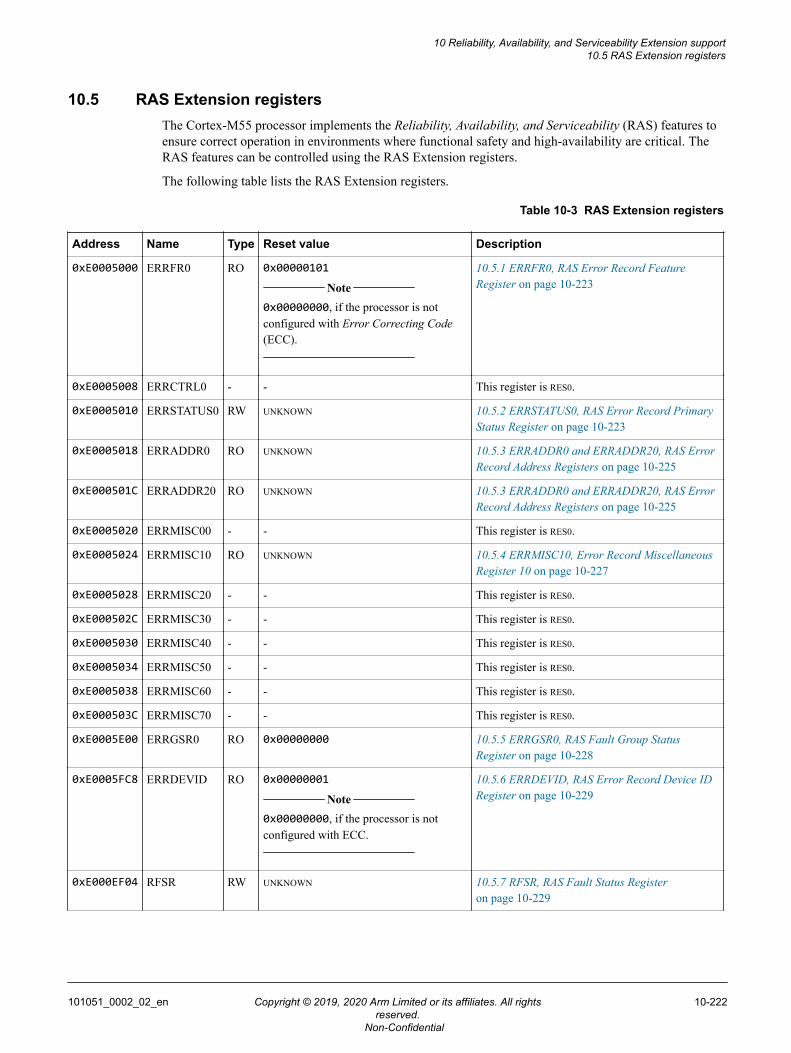
10.5 RAS Extension registersThe Cortex-M55 processor implements the Reliability, Availability, and Serviceability (RAS) features toensure correct operation in environments where functional safety and high-availability are critical. TheRAS features can be controlled using the RAS Extension registers.
The following table lists the RAS Extension registers.
Table 10-3 RAS Extension registers
Address Name Type Reset value Description
0xE0005000 ERRFR0 RO 0x00000101 Note
0x00000000, if the processor is notconfigured with Error Correcting Code(ECC).
10.5.1 ERRFR0, RAS Error Record FeatureRegister on page 10-223
0xE0005008 ERRCTRL0 - - This register is RES0.
0xE0005010 ERRSTATUS0 RW UNKNOWN 10.5.2 ERRSTATUS0, RAS Error Record PrimaryStatus Register on page 10-223
0xE0005018 ERRADDR0 RO UNKNOWN 10.5.3 ERRADDR0 and ERRADDR20, RAS ErrorRecord Address Registers on page 10-225
0xE000501C ERRADDR20 RO UNKNOWN 10.5.3 ERRADDR0 and ERRADDR20, RAS ErrorRecord Address Registers on page 10-225
0xE0005020 ERRMISC00 - - This register is RES0.
0xE0005024 ERRMISC10 RO UNKNOWN 10.5.4 ERRMISC10, Error Record MiscellaneousRegister 10 on page 10-227
0xE0005028 ERRMISC20 - - This register is RES0.
0xE000502C ERRMISC30 - - This register is RES0.
0xE0005030 ERRMISC40 - - This register is RES0.
0xE0005034 ERRMISC50 - - This register is RES0.
0xE0005038 ERRMISC60 - - This register is RES0.
0xE000503C ERRMISC70 - - This register is RES0.
0xE0005E00 ERRGSR0 RO 0x00000000 10.5.5 ERRGSR0, RAS Fault Group StatusRegister on page 10-228
0xE0005FC8 ERRDEVID RO 0x00000001 Note
0x00000000, if the processor is notconfigured with ECC.
10.5.6 ERRDEVID, RAS Error Record Device IDRegister on page 10-229
0xE000EF04 RFSR RW UNKNOWN 10.5.7 RFSR, RAS Fault Status Registeron page 10-229
10 Reliability, Availability, and Serviceability Extension support10.5 RAS Extension registers
101051_0002_02_en Copyright © 2019, 2020 Arm Limited or its affiliates. All rightsreserved.
10-222
Non-Confidential
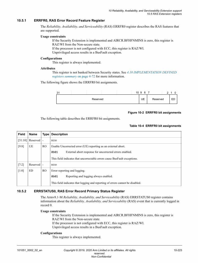
10.5.1 ERRFR0, RAS Error Record Feature Register
The Reliability, Availability, and Serviceability (RAS) ERRFR0 register describes the RAS features thatare supported.
Usage constraintsIf the Security Extension is implemented and AIRCR.BFHFNMINS is zero, this register isRAZ/WI from the Non-secure state.If the processor is not configured with ECC, this register is RAZ/WI.Unprivileged access results in a BusFault exception.
ConfigurationsThis register is always implemented.
AttributesThis register is not banked between Security states. See 4.10 IMPLEMENTATION DEFINEDregisters summary on page 4-72 for more information.
The following figure shows the ERRFR0 bit assignments.
31 02 1
Reserved
10 9 8 7
UE Reserved ED
Figure 10-2 ERRFR0 bit assignments
The following table describes the ERRFR0 bit assignments.
Table 10-4 ERRFR0 bit assignments
Field Name Type Description
[31:10] Reserved - RES0
[9:8] UE RO Enable Uncorrected error (UE) reporting as an external abort.
0b01 External abort response for uncorrected errors enabled.
This field indicates that uncorrectable errors cause BusFault exceptions.
[7:2] Reserved - RES0
[1:0] ED RO Error reporting and logging.
0b01 Reporting and logging always enabled.
This field indicates that logging and reporting of errors cannot be disabled.
10.5.2 ERRSTATUS0, RAS Error Record Primary Status Register
The Armv8.1‑M Reliability, Availability, and Serviceability (RAS) ERRSTATUS0 register containsinformation about the Reliability, Availability, and Serviceability (RAS) event that is currently logged inrecord 0.
Usage constraintsIf the Security Extension is implemented and AIRCR.BFHFNMINS is zero, this register isRAZ/WI from the Non-secure state.If the processor is not configured with ECC, this register is RAZ/WI.Unprivileged access results in a BusFault exception.
ConfigurationsThis register is always implemented.
10 Reliability, Availability, and Serviceability Extension support10.5 RAS Extension registers
101051_0002_02_en Copyright © 2019, 2020 Arm Limited or its affiliates. All rightsreserved.
10-223
Non-Confidential
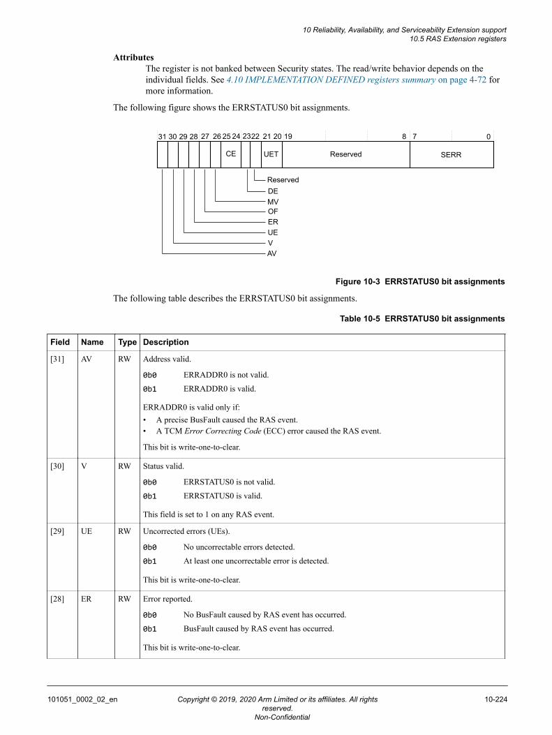
AttributesThe register is not banked between Security states. The read/write behavior depends on theindividual fields. See 4.10 IMPLEMENTATION DEFINED registers summary on page 4-72 formore information.
The following figure shows the ERRSTATUS0 bit assignments.
31 0282930 8 7
Reserved
Reserved
27 26 19
UET SERR
20212225 24 23
CE
DEMVOFERUEVAV
Figure 10-3 ERRSTATUS0 bit assignments
The following table describes the ERRSTATUS0 bit assignments.
Table 10-5 ERRSTATUS0 bit assignments
Field Name Type Description
[31] AV RW Address valid.
0b0 ERRADDR0 is not valid.
0b1 ERRADDR0 is valid.
ERRADDR0 is valid only if:• A precise BusFault caused the RAS event.• A TCM Error Correcting Code (ECC) error caused the RAS event.
This bit is write-one-to-clear.
[30] V RW Status valid.
0b0 ERRSTATUS0 is not valid.
0b1 ERRSTATUS0 is valid.
This field is set to 1 on any RAS event.
[29] UE RW Uncorrected errors (UEs).
0b0 No uncorrectable errors detected.
0b1 At least one uncorrectable error is detected.
This bit is write-one-to-clear.
[28] ER RW Error reported.
0b0 No BusFault caused by RAS event has occurred.
0b1 BusFault caused by RAS event has occurred.
This bit is write-one-to-clear.
10 Reliability, Availability, and Serviceability Extension support10.5 RAS Extension registers
101051_0002_02_en Copyright © 2019, 2020 Arm Limited or its affiliates. All rightsreserved.
10-224
Non-Confidential
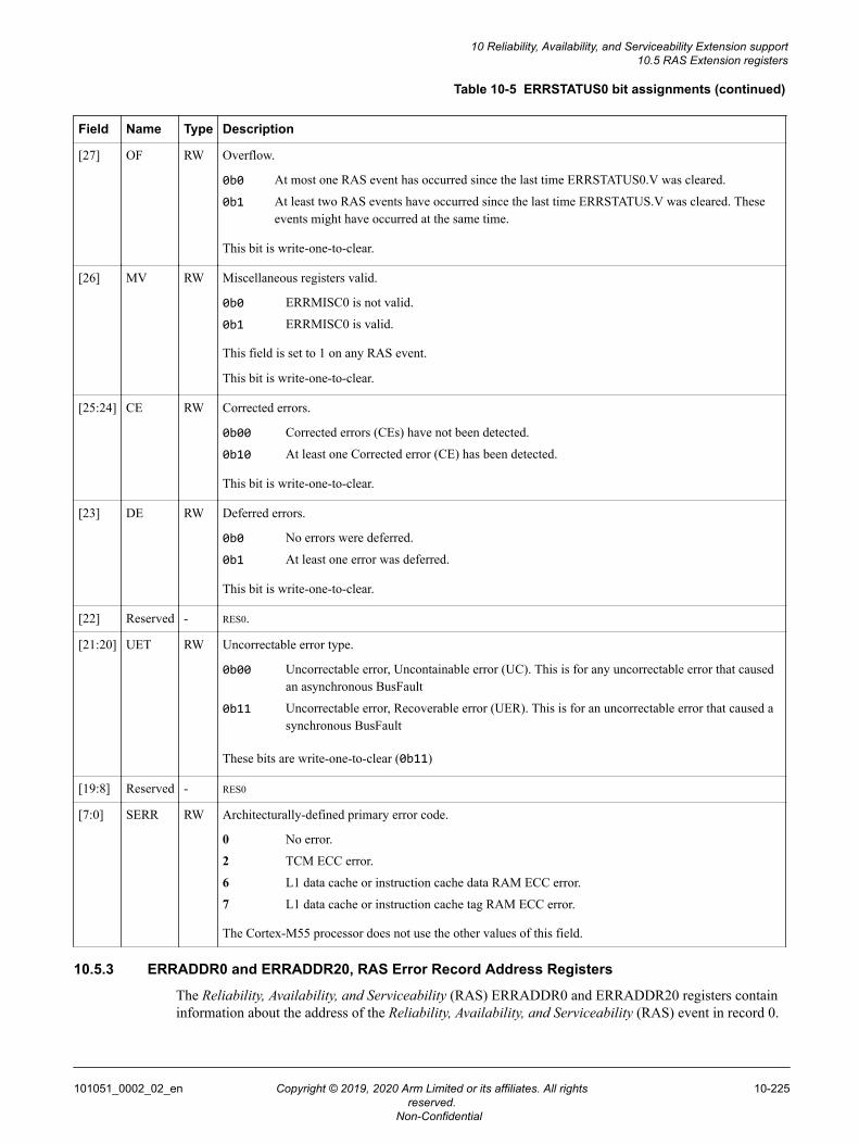
Table 10-5 ERRSTATUS0 bit assignments (continued)
Field Name Type Description
[27] OF RW Overflow.
0b0 At most one RAS event has occurred since the last time ERRSTATUS0.V was cleared.
0b1 At least two RAS events have occurred since the last time ERRSTATUS.V was cleared. Theseevents might have occurred at the same time.
This bit is write-one-to-clear.
[26] MV RW Miscellaneous registers valid.
0b0 ERRMISC0 is not valid.
0b1 ERRMISC0 is valid.
This field is set to 1 on any RAS event.
This bit is write-one-to-clear.
[25:24] CE RW Corrected errors.
0b00 Corrected errors (CEs) have not been detected.
0b10 At least one Corrected error (CE) has been detected.
This bit is write-one-to-clear.
[23] DE RW Deferred errors.
0b0 No errors were deferred.
0b1 At least one error was deferred.
This bit is write-one-to-clear.
[22] Reserved - RES0.
[21:20] UET RW Uncorrectable error type.
0b00 Uncorrectable error, Uncontainable error (UC). This is for any uncorrectable error that causedan asynchronous BusFault
0b11 Uncorrectable error, Recoverable error (UER). This is for an uncorrectable error that caused asynchronous BusFault
These bits are write-one-to-clear (0b11)
[19:8] Reserved - RES0
[7:0] SERR RW Architecturally-defined primary error code.
0 No error.
2 TCM ECC error.
6 L1 data cache or instruction cache data RAM ECC error.
7 L1 data cache or instruction cache tag RAM ECC error.
The Cortex-M55 processor does not use the other values of this field.
10.5.3 ERRADDR0 and ERRADDR20, RAS Error Record Address Registers
The Reliability, Availability, and Serviceability (RAS) ERRADDR0 and ERRADDR20 registers containinformation about the address of the Reliability, Availability, and Serviceability (RAS) event in record 0.
10 Reliability, Availability, and Serviceability Extension support10.5 RAS Extension registers
101051_0002_02_en Copyright © 2019, 2020 Arm Limited or its affiliates. All rightsreserved.
10-225
Non-Confidential
Usage constraintsIf the Security Extension is implemented and AIRCR.BFHFNMINS is zero, this register isRAZ/WI from the Non-secure state.If the processor is not configured with ECC, this register is RAZ/WI.Unprivileged access results in a BusFault exception.This register ignores writes if ERRSTATUS0.AV is set to 1.
ConfigurationsThese registers are always implemented.
AttributesThese registers are not banked between Security states. See 4.10 IMPLEMENTATIONDEFINED registers summary on page 4-72 for more information.
The following figure shows the ERRADDR0 bit assignments.
31 0
PADDR
Figure 10-4 ERRADDR0 bit assignments
The following table describes the ERRADDR0 bit assignments.
Table 10-6 ERRADDR0 bit assignments
Field Name Type Description
[31:0] PADDR RW Address of the RAS event. This is the address associated with the memory access that observed ErrorCorrecting Code (ECC) error. This field is not valid if ERRADDR20.AI is 0b1.
The following figure shows the ERRADDR20 bit assignments.
31 0
RES0
RES1AISIReserved
30 29 28
Figure 10-5 ERRADDR20 bit assignments
The following table describes the ERRADDR20 bit assignments.
Table 10-7 ERRADDR20 bit assignments
Field Name Type Description
[31] Reserved - RES0
[30] SI RO Security information incorrect.
0b1 NS bit is not valid.
The security information is never guaranteed to be correct.
10 Reliability, Availability, and Serviceability Extension support10.5 RAS Extension registers
101051_0002_02_en Copyright © 2019, 2020 Arm Limited or its affiliates. All rightsreserved.
10-226
Non-Confidential
Table 10-7 ERRADDR20 bit assignments (continued)
Field Name Type Description
[29] AI RO Address incorrect.
0b0 PADDR is valid.
0b1 PADDR is not valid.
PADDR is valid only if:• The RAS event was a precise BusFault.• The RAS event was associated with a TCM ECC error.
Note
If software clears ERRSTATUS.AV, then ERRADDR20.AI is set to 0b1 to invalidate the address.
[28] Reserved - RES1
[27:0] Reserved - RES0
10.5.4 ERRMISC10, Error Record Miscellaneous Register 10
The ERRMISC10 register is an IMPLEMENTATION DEFINED error syndrome register for the event in record 0.
Usage constraintsIf the Security Extension is implemented and AIRCR.BFHFNMINS is zero, this register isRAZ/WI from the Non-secure state.If the processor is not configured with Error Correcting Code (ECC), this register is RAZ/WI.Unprivileged access results in a BusFault exception.
ConfigurationsThis register is always implemented.
AttributesThis register is not banked between Security states. See 4.10 IMPLEMENTATION DEFINEDregisters summary on page 4-72 for more information.
The following figure shows the ERRMISC10 bit assignments.
31 0
Reserved TYPE
12
Figure 10-6 ERRMISC10 bit assignments
10 Reliability, Availability, and Serviceability Extension support10.5 RAS Extension registers
101051_0002_02_en Copyright © 2019, 2020 Arm Limited or its affiliates. All rightsreserved.
10-227
Non-Confidential
The following table describes the ERRMISC10 bit assignments.
Table 10-8 ERRMISC10 bit assignments
Field Name Type Description
[31:2] Reserved - RES0
[1:0] TYPE RO Indicates the type of Reliability, Availability, and Serviceability (RAS) event logged.
0b00 L1 instruction cache ECC.
0b01 L1 data cache ECC.
0b10 TCM ECC found by load or store executed by the processor.
0b11 TCM ECC found by access from Slave AHB (S-AHB).
Note
In the Cortex-M55 processor, only ERRMISC10 is implemented. ERRMISC00 and ERRMISC20-ERRMISC70 are RES0.
10.5.5 ERRGSR0, RAS Fault Group Status Register
The ERRGSR0 register summarizes the valid error records. The Cortex-M55 processor only supportsone error record, therefore, only one bit of ERRGSR is active.
Usage constraintsIf the Security Extension is implemented and AIRCR.BFHFNMINS is zero, this register isRAZ/WI from the Non-secure state.If the processor is not configured with Error Correcting Code (ECC), this register is RAZ/WI.Unprivileged access results in a BusFault exception.
ConfigurationsThis register is always implemented.
AttributesThis register is not banked between Security states. See 4.10 IMPLEMENTATION DEFINEDregisters summary on page 4-72 for more information.
The following figure shows the ERRGSR0 bit assignments.
31 0
Reserved
ERR0
1
Figure 10-7 ERRGSR0 bit assignments
The following table describes the ERRGSR0 bit assignments.
Table 10-9 ERRGSR0 bit assignments
Field Name Type Description
[31:1] Reserved - RES0
[0] ERR0 RO Error record 0 is valid.
10 Reliability, Availability, and Serviceability Extension support10.5 RAS Extension registers
101051_0002_02_en Copyright © 2019, 2020 Arm Limited or its affiliates. All rightsreserved.
10-228
Non-Confidential
10.5.6 ERRDEVID, RAS Error Record Device ID Register
The Reliability, Availability, and Serviceability (RAS) ERRDEVID register contains the number of errorrecords that an implementation supports. The Cortex-M55 processor supports a single error record withindex 0 if Error Correcting Code (ECC) is configured or there are no error records.
Usage constraintsUnprivileged access results in a BusFault exception.This register is accessible through unprivileged Debug AHB (D-AHB) debug requests wheneither DAUTHCTRL_S.UIDAPEN or DAUTHCTRL_NS.UIDAPEN is set.
ConfigurationsThis register is always implemented.
AttributesThis register is not banked between Security states. See 4.10 IMPLEMENTATION DEFINEDregisters summary on page 4-72 for more information.
The following figure shows the ERRDEVID bit assignments.
31 0
Reserved NUM
16 15
Figure 10-8 ERRDEVID bit assignments
The following table describes the ERRDEVID bit assignments.
Table 10-10 ERRDEVID bit assignments
Field Name Type Description
[31:16] Reserved - RES0
[15:0] NUM RO Maximum Error Record Index+1
0x0001 If ECC is configured, then one error record with index 0.
0x0000 If ECC is not configured, then there are no error record registers.
10.5.7 RFSR, RAS Fault Status Register
The RFSR reports the fault status of Reliability, Availability, and Serviceability (RAS) related faults fromError Correcting Code (ECC) errors that are detected in the L1 instruction cache, data cache, and TCM.
Usage constraintsIf the Security Extension is implemented and AIRCR.BFHFNMINS is zero, this register isRAZ/WI from Non-secure state.If the processor is not configured with Error Correcting Code (ECC), this register is RAZ/WI.Unprivileged access results in a BusFault exception.
ConfigurationsThis register is always implemented.
AttributesThis is register are not banked between Security states. See 4.10 IMPLEMENTATIONDEFINED registers summary on page 4-72 for more information.
The following figure shows the RFSR bit assignments.
10 Reliability, Availability, and Serviceability Extension support10.5 RAS Extension registers
101051_0002_02_en Copyright © 2019, 2020 Arm Limited or its affiliates. All rightsreserved.
10-229
Non-Confidential
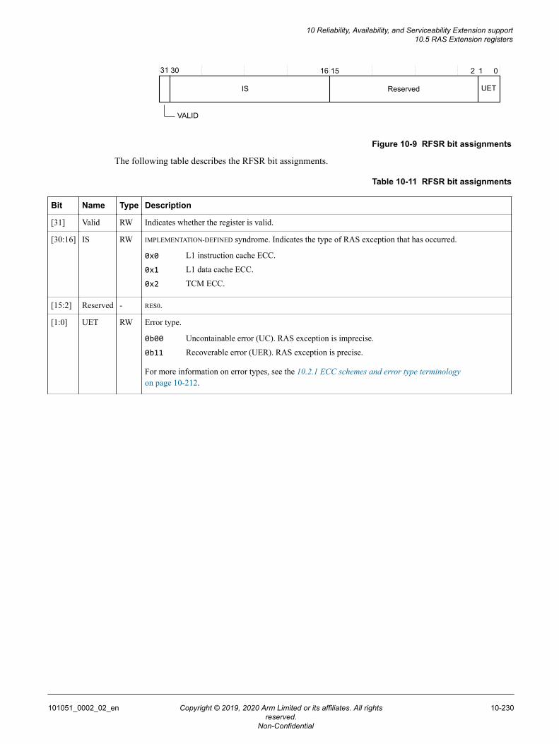
31 16 15 0
ReservedIS
30
VALID
1
UET
2
Figure 10-9 RFSR bit assignments
The following table describes the RFSR bit assignments.
Table 10-11 RFSR bit assignments
Bit Name Type Description
[31] Valid RW Indicates whether the register is valid.
[30:16] IS RW IMPLEMENTATION-DEFINED syndrome. Indicates the type of RAS exception that has occurred.
0x0 L1 instruction cache ECC.
0x1 L1 data cache ECC.
0x2 TCM ECC.
[15:2] Reserved - RES0.
[1:0] UET RW Error type.
0b00 Uncontainable error (UC). RAS exception is imprecise.
0b11 Recoverable error (UER). RAS exception is precise.
For more information on error types, see the 10.2.1 ECC schemes and error type terminologyon page 10-212.
10 Reliability, Availability, and Serviceability Extension support10.5 RAS Extension registers
101051_0002_02_en Copyright © 2019, 2020 Arm Limited or its affiliates. All rightsreserved.
10-230
Non-Confidential
Chapter 11Nested Vectored Interrupt Controller
This chapter describes the Nested Vectored Interrupt Controller (NVIC).
It contains the following sections:• 11.1 NVIC features on page 11-232.• 11.2 Registers associated with interrupt control and behavior on page 11-233.• 11.3 NVIC register summary on page 11-234.• 11.4 Software Interrupt Generation register summary on page 11-235.• 11.5 SysTick Timer register summary on page 11-236.
101051_0002_02_en Copyright © 2019, 2020 Arm Limited or its affiliates. All rightsreserved.
11-231
Non-Confidential
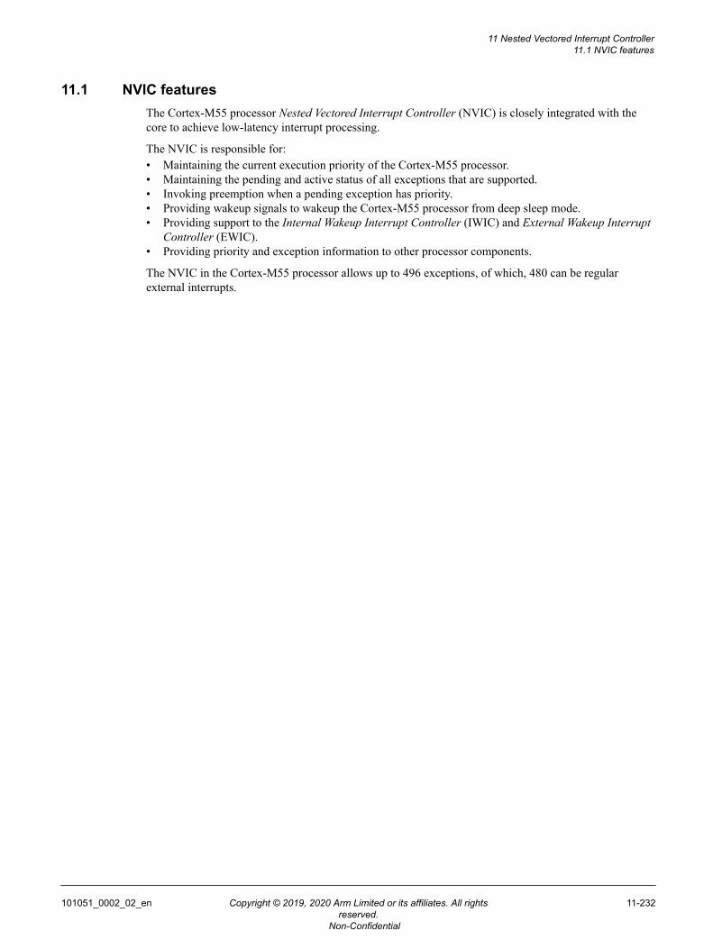
11.1 NVIC featuresThe Cortex-M55 processor Nested Vectored Interrupt Controller (NVIC) is closely integrated with thecore to achieve low-latency interrupt processing.
The NVIC is responsible for:• Maintaining the current execution priority of the Cortex-M55 processor.• Maintaining the pending and active status of all exceptions that are supported.• Invoking preemption when a pending exception has priority.• Providing wakeup signals to wakeup the Cortex-M55 processor from deep sleep mode.• Providing support to the Internal Wakeup Interrupt Controller (IWIC) and External Wakeup Interrupt
Controller (EWIC).• Providing priority and exception information to other processor components.
The NVIC in the Cortex-M55 processor allows up to 496 exceptions, of which, 480 can be regularexternal interrupts.
11 Nested Vectored Interrupt Controller11.1 NVIC features
101051_0002_02_en Copyright © 2019, 2020 Arm Limited or its affiliates. All rightsreserved.
11-232
Non-Confidential
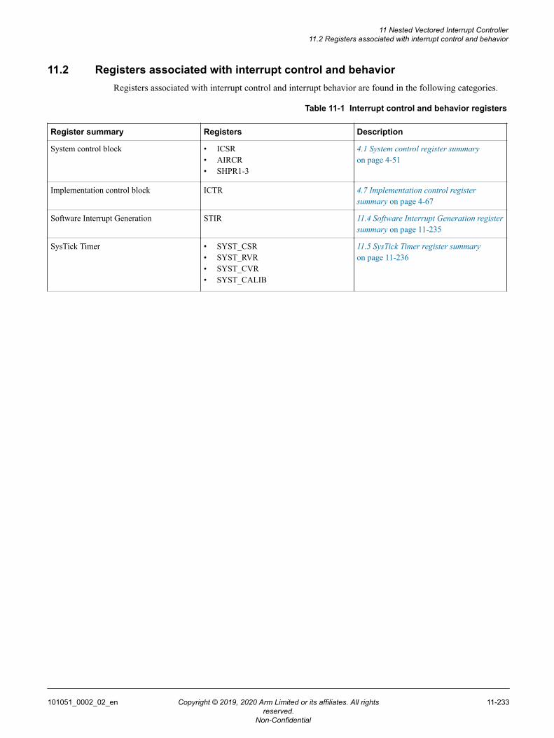
11.2 Registers associated with interrupt control and behaviorRegisters associated with interrupt control and interrupt behavior are found in the following categories.
Table 11-1 Interrupt control and behavior registers
Register summary Registers Description
System control block • ICSR• AIRCR• SHPR1-3
4.1 System control register summaryon page 4-51
Implementation control block ICTR 4.7 Implementation control registersummary on page 4-67
Software Interrupt Generation STIR 11.4 Software Interrupt Generation registersummary on page 11-235
SysTick Timer • SYST_CSR• SYST_RVR• SYST_CVR• SYST_CALIB
11.5 SysTick Timer register summaryon page 11-236
11 Nested Vectored Interrupt Controller11.2 Registers associated with interrupt control and behavior
101051_0002_02_en Copyright © 2019, 2020 Arm Limited or its affiliates. All rightsreserved.
11-233
Non-Confidential
11.3 NVIC register summaryThe Nested Vectored Interrupt Controller (NVIC) registers can be accesses through the Internal PrivatePeripheral Bus (IPPB) interface. Each of the NVIC registers is 32 bits wide.
The NVIC_ISERn, NVIC_ICERn, NVIC_ISPRn, NVIC_ICPRn, NVIC_IABRn, and NVIC_IPRnregisters are not banked between Security states. If an interrupt is configured as Secure in theNVIC_ITNSn register, any access to the corresponding NVIC_ISERn, NVIC_ICERn, NVIC_ISPRn,NVIC_ICPRn, NVIC_IABRn, or NVIC_IPRn registers from Non-secure are treated as RAZ/WI.
For more information on the NVIC registers listed in the following table, see Arm®v8-M ArchitectureReference Manual.
Table 11-2 NVIC register summary
Address offset Name Type Reset value Description
0xE000E100-0xE000E13C NVIC_ISER0-NVIC_ISER15
RW 0x00000000 Interrupt Set-Enable Registers
0xE000E180-0xE000E1BC NVIC_ICER0-NVIC_ICER15
RW 0x00000000 Interrupt Clear-Enable Registers
0xE000E200-0xE000E23C NVIC_ISPR0-NVIC_ISPR15
RW 0x00000000 Interrupt Set-Pending Registers
0xE000E280-0xE000E2BC NVIC_ICPR0-NVIC_ICPR15
RW 0x00000000 Interrupt Clear-Pending Registers
0xE000E300-0xE000E33C NVIC_IABR0-NVIC_IABR15
RO 0x00000000 Interrupt Active Bit Register
0xE000E380-0xE000E3BC NVIC_ITNS0-NVIC_ITNS15
RW 0x00000000 Interrupt Target Non-secure Registers Note
These registers are Secure only. They are RAZ/WIwhen accessed from Non-secure state.
0xE000E400-0xE000E5DC NVIC_IPR0-NVIC_IPR119
RW 0x00000000 Interrupt Priority Registers
11 Nested Vectored Interrupt Controller11.3 NVIC register summary
101051_0002_02_en Copyright © 2019, 2020 Arm Limited or its affiliates. All rightsreserved.
11-234
Non-Confidential
11.4 Software Interrupt Generation register summaryThe following table shows the architecturally defined Software Interrupt Generation register.
Table 11-3 Software Interrupt Generation register summary
Address offset Name Type Reset value Description
0xE000EF00 STIR WO 0x00000000 Software Triggered Interrupt Register. For more information, see Arm®v8-MArchitecture Reference Manual.
11 Nested Vectored Interrupt Controller11.4 Software Interrupt Generation register summary
101051_0002_02_en Copyright © 2019, 2020 Arm Limited or its affiliates. All rightsreserved.
11-235
Non-Confidential
11.5 SysTick Timer register summaryThe following table shows the architecturally defined SysTick Timer registers.
Note
For more information on the architectural registers listed in the following table, see the Arm®v8-MArchitecture Reference Manual.
Table 11-4 SysTick Timer register summary
Address offset Name Type Reset value Description
0xE000E010 SYST_CSR RW 0x00000000 SysTick Control and Status Register
0xE000E014 SYST_RVR RW 0x00000000 SysTick Reload Value Register
0xE000E018 SYST_CVR RW 0x00000000 SysTick Current Value Register
0xE000E01C SYST_CALIB RO 0x00000000 SysTick Calibration Value Register
11 Nested Vectored Interrupt Controller11.5 SysTick Timer register summary
101051_0002_02_en Copyright © 2019, 2020 Arm Limited or its affiliates. All rightsreserved.
11-236
Non-Confidential
Chapter 12External coprocessors
This chapter describes the interface and programmer's model for connecting and using externalcoprocessors.
It contains the following sections:• 12.1 External coprocessors features on page 12-238.• 12.2 Operation on page 12-239.• 12.3 Data transfer rates on page 12-240.• 12.4 Coprocessor instruction restrictions on page 12-241.• 12.5 Debug access to coprocessor registers usage constraints on page 12-242.• 12.6 Exceptions and context switch on page 12-243.• 12.7 Response to coprocessor errors on page 12-244.• 12.8 Hazard between load and store instructions followed by coprocessor transactions
on page 12-245.
101051_0002_02_en Copyright © 2019, 2020 Arm Limited or its affiliates. All rightsreserved.
12-237
Non-Confidential
12.1 External coprocessors featuresThe Cortex-M55 processor supports an external coprocessor interface which allows the integration oftightly coupled accelerator hardware with the processor. The programmers model allows software tocommunicate with the hardware by using architectural coprocessor instructions.
The external coprocessor interface:• Supports low-latency data transfer from the processor to and from the accelerator components.• Provides a mechanism for you to extend the capabilities of the Cortex-M55 processor.• Supports up to eight separate coprocessors, CP0-CP7, depending on your implementation. The
remaining coprocessor numbers, CP8-CP15, are reserved. CP10 and CP11 are always reserved forfloating-point or M‑profile Vector Extension (MVE) functionality. For more information, see theArm®v8-M Architecture Reference Manual. The Cortex-M55 processor system can configure whichcoprocessor is included in Secure and Non-secure states.
12 External coprocessors12.1 External coprocessors features
101051_0002_02_en Copyright © 2019, 2020 Arm Limited or its affiliates. All rightsreserved.
12-238
Non-Confidential
12.2 OperationThe external coprocessor interface provides control and data channels for up to eight separatecoprocessors. The external devices are provided with information about privilege and Security state ofthe processor with the instruction type and associate register and operation fields that the architecturedefines. The following instruction types are supported:
• Register transfer from the Cortex-M55 processor to the coprocessor MCR, MCRR, MCR2, MCRR2.• Register transfer from the coprocessor to the Cortex-M55 processor MRC, MRRC, MRC2, MRRC2.• Data processing instructions CDP, CDP2.
The interface provides a handshake mechanism to indicate to the coprocessor that an instruction has beencommitted in the processor and can no longer be interrupted. Additionally, it can stall the processor in away that it can always be interrupted (BUSYWAIT) and to indicate that an error has occurred whilewaiting for an UNDEFINSTR UsageFault.
Note
• The regular and extension forms of the coprocessor instructions for example, MCR and MCRR2, have thesame functionality but different encodings. The two encoding values differ by a single bit, bit [12].For more information, see the Arm®v8-M Architecture Reference Manual.
• The MRC and MRC2 instructions support the transfer of APSR.NZVC flags when the processor registerfield is set to PC, for example Rt == 0xF.
12 External coprocessors12.2 Operation
101051_0002_02_en Copyright © 2019, 2020 Arm Limited or its affiliates. All rightsreserved.
12-239
Non-Confidential
12.3 Data transfer ratesThe following table lists the ideal data transfer rates for the coprocessor interface. This means that thecoprocessor responds to an instruction immediately and does not BUSYWAIT. The ideal data transferrates are sustainable if the corresponding coprocessor instructions are executed consecutively.
Table 12-1 Ideal data transfer rates for the coprocessor interface
Instructions Direction Ideal data rate
MCR, MCR2 Processor to coprocessor 32 bits per cycle
MRC, MRC2 Coprocessor to processor 32 bits per cycle
MCRR, MCRR2 Processor to coprocessor 64 bits per cycle
MRRC, MRRC2 Coprocessor to processor 64 bits per cycle
12 External coprocessors12.3 Data transfer rates
101051_0002_02_en Copyright © 2019, 2020 Arm Limited or its affiliates. All rightsreserved.
12-240
Non-Confidential
12.4 Coprocessor instruction restrictionsThe following restrictions apply when the Cortex-M55 processor uses coprocessor instructions:
• The LDC(2) or STC(2) instructions are not supported. If these are included in software with the<coproc> field set to a value between 0-7 and the coprocessor is present and enabled in theappropriate fields in the CPACR or NSACR, the Cortex-M55 processor always attempts to take anUndefined instruction (UNDEFINSTR) UsageFault exception.
• The processor register fields for data transfer instructions must not include the stack pointer (Rt =0xD), this encoding is UNPREDICTABLE in the Armv8.1‑M architecture and results in an UNDEFINSTRUsageFault exception in the Cortex-M55 processor if the coprocessor is present and enabled in theCPACR or NSACR.
• If any coprocessor instruction is executed when the corresponding coprocessor is either not present ordisabled in the CPACR or NSACR, the Cortex-M55 processor always attempts to take a Nocoprocessor (NOCP) UsageFault exception.
For more information on the CPACR and NSACR, see the Arm®v8-M Architecture Reference Manual.
12 External coprocessors12.4 Coprocessor instruction restrictions
101051_0002_02_en Copyright © 2019, 2020 Arm Limited or its affiliates. All rightsreserved.
12-241
Non-Confidential
12.5 Debug access to coprocessor registers usage constraintsThe Cortex-M55 processor does not support a mechanism to read and write registers located in externalcoprocessors.
Arm recommends that you implement a coprocessor with a dedicated AHB or APB slave interface forthe system to access the registers. If the debug view of the coprocessor is located in the PPB region ofthe memory map, you can use this interface to connect to the External Private Peripheral Bus (EPPB)interface of the Cortex-M55 processor.
If Secure debug is disabled, you must ensure the Secure information in the coprocessors is protected andnot accessible when using a Non-secure debugger.
If the debug slave interface to the coprocessor is connected to the processor Master AXI (M-AXI) orPeripheral AHB (P-AHB) master interfaces or the EPPB interface, you can use the ARPROT[1],AWPROT[1], HNONSEC, and PPROT[2] signals on the M-AXI and P-AHB, and APB interfacesrespectively. This is because the security level of the debug requests routed through the processor fromthe D-AHB interface are subject to the debug access and authentication checks.
If the coprocessor state is memory-mapped, then software can also access the information using load andstore instructions. If your implementation uses this functionality, you must ensure the appropriate barrierinstructions are included to guarantee ordering between coprocessor instructions and load/storeoperations to the same state.
12 External coprocessors12.5 Debug access to coprocessor registers usage constraints
101051_0002_02_en Copyright © 2019, 2020 Arm Limited or its affiliates. All rightsreserved.
12-242
Non-Confidential
12.6 Exceptions and context switchThe Cortex-M55 processor does not include support for automatic save and restore of coprocessorregisters on entry and exit to exceptions, unlike the internal processor integer and floating-point registers.Any coprocessor state that must be maintained across a context switch must be carried out by thesoftware that is aware of the coprocessor requirements.
You must ensure that when the coprocessor contains Secure data, it cannot be accessed by softwarerunning in a Non-secure exception handler.
12 External coprocessors12.6 Exceptions and context switch
101051_0002_02_en Copyright © 2019, 2020 Arm Limited or its affiliates. All rightsreserved.
12-243
Non-Confidential
12.7 Response to coprocessor errorsThe coprocessor must not rely on a synchronous exception that is taken when asserting a CPERRORresponse to a coprocessor transaction, because the UNDEFINSTR UsageFault might be preempted by ahigher priority interrupt in the Cortex-M55 processor. There is no guarantee that there are no side effectsfrom the erroneous instruction.
12 External coprocessors12.7 Response to coprocessor errors
101051_0002_02_en Copyright © 2019, 2020 Arm Limited or its affiliates. All rightsreserved.
12-244
Non-Confidential
12.8 Hazard between load and store instructions followed by coprocessortransactions
A possible hazard exists when a load and store instruction is followed by coprocessor transactions.
To decouple the data side TCMWAIT input signal from the CPVALID output signal, a coprocessorinstruction following a load or store instruction the processor always stalls for a clock cycle after the loador store completes.
This does not add any additional stall cycles to the data hazard that is already included in the mostcommon case where the result of a load is consumed by a coprocessor data transfer instruction.
12 External coprocessors12.8 Hazard between load and store instructions followed by coprocessor transactions
101051_0002_02_en Copyright © 2019, 2020 Arm Limited or its affiliates. All rightsreserved.
12-245
Non-Confidential
Chapter 13Floating-point and MVE support
This chapter describes the Extension Processing Unit (EPU), which controls floating-point and M-profileVector Extension (MVE) support.
It contains the following sections:• 13.1 Floating-point and MVE operation on page 13-247.• 13.2 Floating-point and MVE register summary on page 13-249.• 13.3 FPDSCR and FPSCR register reset values on page 13-250.• 13.4 Powering down the EPU on page 13-251.
101051_0002_02_en Copyright © 2019, 2020 Arm Limited or its affiliates. All rightsreserved.
13-246
Non-Confidential
13.1 Floating-point and MVE operationThe Extension Processing Unit (EPU) can be configured to perform floating-point and M‑profile VectorExtension (MVE) operations.
Scalar floating-point operationThe Cortex-M55 processor can be configured to provide scalar half, single, and double-precision floating-point operation. The floating-point operation is an implementation of thescalar half, single, and double-precision variants of the Floating-point Extension, FPv5architecture. Configuring the processor to include floating-point supports all half, single, anddouble-precision data-processing instructions and data types described in the Arm®v8-MArchitecture Reference Manual.The processor supports scalar half, single, and double-precision add, subtract, multiply, divide,multiply and accumulate, and square root operations. The floating-point functionality that theprocessor supports also provides conversions between fixed-point and floating-point dataformats, and floating-point constant instructions.
M-profile Vector Extension operationThe Cortex-M55 processor can be configured to provide MVE operation. The MVEfunctionality that is supported depends on the inclusion of floating-point functionality.• If floating-point functionality is not included, the processor can be configured to any of the
following:— Not include MVE.— Include the integer subset of MVE only (MVE-I). MVE-I operates on 8-bit, 16-bit, and
32-bit data types.
• If floating-point functionality is included, the processor can be configured to any of thefollowing:— Not include MVE.— Include the integer subset of MVE only (MVE-I). MVE-I operates on 8-bit, 16-bit, and
32-bit data types.— Include the integer, half-precision, and single-precision floating-point MVE (MVE-F).
MVE-F operates on half-precision and single-precision floating-point values. MVE-Falso includes support for MVE-I.
Vector instructions operate on a fixed vector width of 128 bits. The lane width of an operation tobe performed is specified by the instruction that is being executed. And an element refers to thedata that is put into a lane. Multiple lanes can be executed per beat. There are four beats pervector instruction.
For more information on the MVE extension and terminology, see Arm®v8-M ArchitectureReference Manual.
Note
• The Cortex-M55 processor provides floating-point computation functionality included with the MVEand Floating-point Extension, which is compliant with the ANSI/IEEE Std 754-2008, IEEE Standardfor Binary Floating-Point Arithmetic.
• The scalar Floating-point Extension can be implemented with or without M‑profile Vector Extension -floating-point (MVE-F).
13.1.1 EPU views of the register bank
The Extension Processing Unit (EPU) provides an extension register file with registers that can beviewed as:
• Thirty-two 32-bit single-word registers, S0-S31.• Sixteen 64-bit doubleword registers, D0-D15.
13 Floating-point and MVE support13.1 Floating-point and MVE operation
101051_0002_02_en Copyright © 2019, 2020 Arm Limited or its affiliates. All rightsreserved.
13-247
Non-Confidential
• Eight 128-bit vector registers, Q0-Q7.• A combination of registers from these views.
13.1.2 Modes of operation
The Cortex-M55 processor supports the following modes of operation:
• Flush to-zero• Half-precision flush to-zero• Default NaN
For more information on these modes, see the Arm®v8-M Architecture Reference Manual.
13.1.3 Compliance with the IEEE 754 standard
The Cortex-M55 processor provides floating-point computation functionality included with the MVEand Floating-point Extension, which is compliant with the ANSI/IEEE Std 754-2008, IEEE Standard forBinary Floating-Point Arithmetic. No support code is required to achieve this compliance.
13.1.4 Exceptions
The Extension Processing Unit (EPU) sets the cumulative exception status flag in the FPSCR register asrequired for each instruction, in accordance with the FPv5 architecture. The EPU does not supportexception traps.
The processor also has six output pins, each pin reflects the status of one of the cumulative exceptionflags:• Inexact result.• The input is denormal.• Overflow.• Underflow.• Divide-by-zero.• Invalid operation
13 Floating-point and MVE support13.1 Floating-point and MVE operation
101051_0002_02_en Copyright © 2019, 2020 Arm Limited or its affiliates. All rightsreserved.
13-248
Non-Confidential
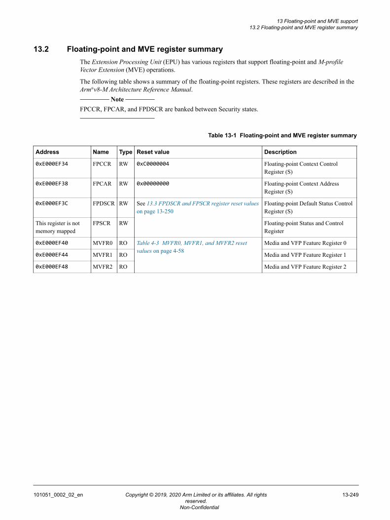
13.2 Floating-point and MVE register summaryThe Extension Processing Unit (EPU) has various registers that support floating-point and M-profileVector Extension (MVE) operations.
The following table shows a summary of the floating-point registers. These registers are described in theArm®v8-M Architecture Reference Manual.
Note
FPCCR, FPCAR, and FPDSCR are banked between Security states.
Table 13-1 Floating-point and MVE register summary
Address Name Type Reset value Description
0xE000EF34 FPCCR RW 0xC0000004 Floating-point Context ControlRegister (S)
0xE000EF38 FPCAR RW 0x00000000 Floating-point Context AddressRegister (S)
0xE000EF3C FPDSCR RW See 13.3 FPDSCR and FPSCR register reset valueson page 13-250
Floating-point Default Status ControlRegister (S)
This register is notmemory mapped
FPSCR RW Floating-point Status and ControlRegister
0xE000EF40 MVFR0 RO Table 4-3 MVFR0, MVFR1, and MVFR2 resetvalues on page 4-58
Media and VFP Feature Register 0
0xE000EF44 MVFR1 RO Media and VFP Feature Register 1
0xE000EF48 MVFR2 RO Media and VFP Feature Register 2
13 Floating-point and MVE support13.2 Floating-point and MVE register summary
101051_0002_02_en Copyright © 2019, 2020 Arm Limited or its affiliates. All rightsreserved.
13-249
Non-Confidential
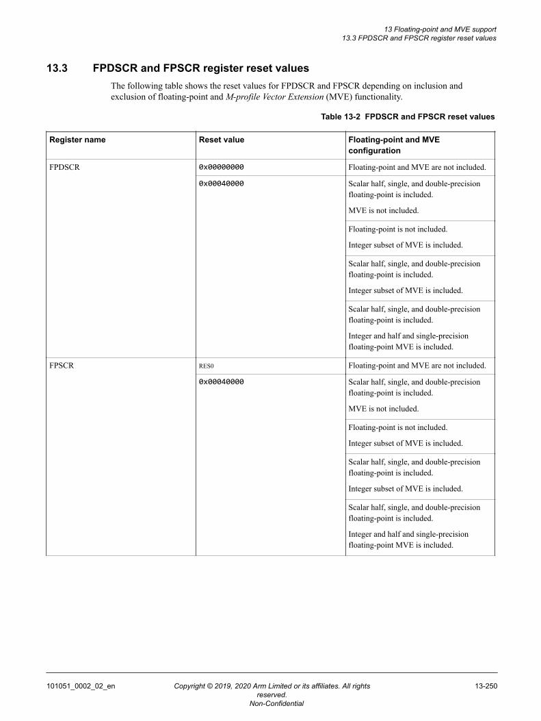
13.3 FPDSCR and FPSCR register reset valuesThe following table shows the reset values for FPDSCR and FPSCR depending on inclusion andexclusion of floating-point and M-profile Vector Extension (MVE) functionality.
Table 13-2 FPDSCR and FPSCR reset values
Register name Reset value Floating-point and MVEconfiguration
FPDSCR 0x00000000 Floating-point and MVE are not included.
0x00040000 Scalar half, single, and double-precisionfloating-point is included.
MVE is not included.
Floating-point is not included.
Integer subset of MVE is included.
Scalar half, single, and double-precisionfloating-point is included.
Integer subset of MVE is included.
Scalar half, single, and double-precisionfloating-point is included.
Integer and half and single-precisionfloating-point MVE is included.
FPSCR RES0 Floating-point and MVE are not included.
0x00040000 Scalar half, single, and double-precisionfloating-point is included.
MVE is not included.
Floating-point is not included.
Integer subset of MVE is included.
Scalar half, single, and double-precisionfloating-point is included.
Integer subset of MVE is included.
Scalar half, single, and double-precisionfloating-point is included.
Integer and half and single-precisionfloating-point MVE is included.
13 Floating-point and MVE support13.3 FPDSCR and FPSCR register reset values
101051_0002_02_en Copyright © 2019, 2020 Arm Limited or its affiliates. All rightsreserved.
13-250
Non-Confidential
13.4 Powering down the EPUDepending on your implementation, the Extension Processing Unit (EPU) can be in a separate powerdomain, PDEPU. The way the EPU power domain is powered down depends on whether the EPUdomain includes state retention logic.
For more information on powering down the EPU, see 6.7 PDEPU low-power requirementson page 6-136.
13 Floating-point and MVE support13.4 Powering down the EPU
101051_0002_02_en Copyright © 2019, 2020 Arm Limited or its affiliates. All rightsreserved.
13-251
Non-Confidential
Chapter 14Debug
This chapter describes the debug system.
It contains the following sections:• 14.1 Debug functionality on page 14-253.• 14.2 D-AHB interface on page 14-259.
101051_0002_02_en Copyright © 2019, 2020 Arm Limited or its affiliates. All rightsreserved.
14-252
Non-Confidential
14.1 Debug functionalityThe Cortex-M55 processor debug functionality includes Armv8‑M, Armv8.1‑M, and CoreSight featuresthat are designed to support debug and trace of software running on the processor.
These features include:• A Breakpoint Unit (BPU) which can be configured to support four or eight hardware breakpoints.• A Data Watchpoint and Trace (DWT) unit which can be configured to support two or four hardware
comparators that can match both address and data values.• Support for the Digital Signal Processing (DSP) debug extension for analysis of signal processing
and compute-based software.• Monitor mode exception for self-hosted debug.• Full access to the memory map and registers through a 32-bit Debug AHB (D-AHB) interface.• An Instrumentation Trace Macrocell (ITM) for software-driven printf debugging which can be
linked to the DWT.• An implementation of the Performance Monitoring Unit (PMU).• An Embedded Trace Macrocell (ETM) which supports complete instruction trace. It implements the
ETMv4.5 architecture, including support for tracing the M‑profile Vector Extension (MVE) features.Data trace is not supported. For more information on the ETM, see the Arm® CoreSight™ ETM‑M55Technical Reference Manual.
• Access control that prevents unauthorized debug or trace of Secure state or memory, includingsupport for the Unprivileged Debug Extension for fine-grain control of debug access to the processor.
Note
• Except for debug monitor mode, all other debug and trace functionality on the Cortex-M55 processoris optional.
• The Cortex-M55 processor is also supplied with an optional Trace Port Interface Unit (TPIU). Formore information, see Appendix B Trace Port Interface Unit on page Appx-B-349.
14.1.1 CoreSight™ discovery
Arm recommends that a debugger identifies and connects to the debug components using the CoreSightdebug infrastructure.
See the Arm® CoreSight™ System-on-Chip SoC-600 Technical Reference Manual for more information.
Arm recommends that a debugger follows the flow in the following figure to discover the componentspresent in the CoreSight debug infrastructure. In this case, for each CoreSight component in theCoreSight system, a debugger reads:
• The peripheral and component ID registers.• The DEVARCH and DEVTYPE registers.
14 Debug14.1 Debug functionality
101051_0002_02_en Copyright © 2019, 2020 Arm Limited or its affiliates. All rightsreserved.
14-253
Non-Confidential
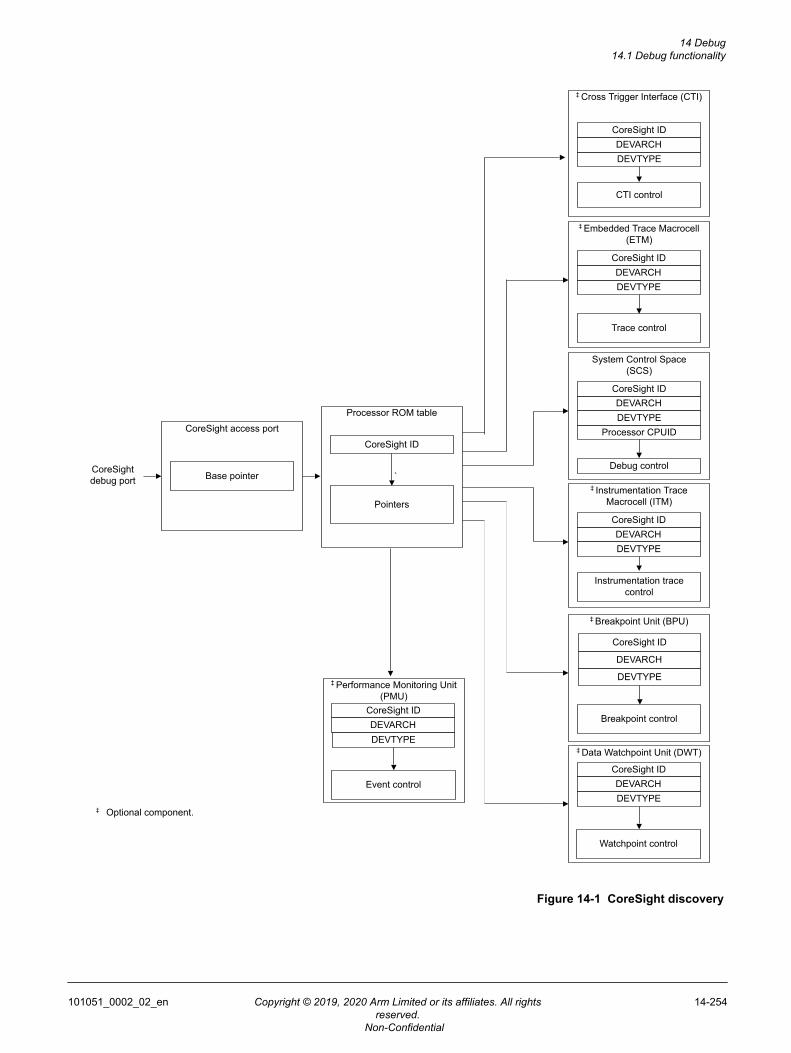
‡ Optional component.
Instrumentation tracecontrol
System Control Space(SCS)
CoreSight ID
Processor CPUID
Debug control
‡ Instrumentation Trace Macrocell (ITM)
Breakpoint control
‡ Breakpoint Unit (BPU)
Watchpoint control
‡ Data Watchpoint Unit (DWT)
‡ Embedded Trace Macrocell (ETM)
Trace control
CoreSight debug port
CoreSight access port
Base pointer
Processor ROM table
Pointers
CoreSight ID
CoreSight IDDEVARCHDEVTYPE
DEVARCHDEVTYPE
CoreSight IDDEVARCHDEVTYPE
CoreSight ID
DEVARCH
DEVTYPE
CoreSight IDDEVARCHDEVTYPE
`
Event control
‡ Performance Monitoring Unit (PMU)
CoreSight IDDEVARCHDEVTYPE
‡ Cross Trigger Interface (CTI)
CoreSight ID
CTI control
DEVARCHDEVTYPE
Figure 14-1 CoreSight discovery
14 Debug14.1 Debug functionality
101051_0002_02_en Copyright © 2019, 2020 Arm Limited or its affiliates. All rightsreserved.
14-254
Non-Confidential
To identify the Cortex-M55 processor and debug components within the CoreSight system, Armrecommends that a debugger performs the following actions:1. Locate and identify the Cortex-M55 processor ROM table using its CoreSight identification.2. Follow the pointers in the Cortex-M55 processor ROM table to identify the presence of the following
components:a. Cross Trigger Interface (CTI)b. Embedded Trace Macrocell (ETM)c. System Control Space (SCS)d. Instrumentation Trace Macrocell (ITM)e. Breakpoint Unit (BPU)f. Data Watchpoint and Trace (DWT) unitg. Performance Monitoring Unit (PMU)
14.1.2 Debugger actions for identifying the processor
When a debugger identifies the System Control Space (SCS) from its CoreSight identification, it canidentify the processor and its revision number from the CPUID register in the SCS at address0xE000ED00.
A debugger cannot rely on the Cortex-M55 processor ROM table being the first ROM table encountered.One or more system ROM tables might be included between the access port and the processor ROMtable if other CoreSight components are in the system. If a system ROM table is present, it can include aunique identifier for the implementation.
14.1.3 Processor ROM table identification and entries
The ROM table identification registers and its values that the following table shows allow debuggers toidentify the processor and its debug capabilities.
The following table shows the CoreSight components that the Cortex-M55 processor ROM table pointsto.
Table 14-1 Cortex-M55 processor ROM table components
Address Component Reset value Description
0xE00FF000 System Control Space(SCS)
0xFFF0F003 See 14.1.4 Debug identification blockregister summary on page 14-257
0xE00FF004 Data Watchpoint andTrace (DWT)
• If DWT is configured,0xFFF02003.
• If DWT is not implemented,0xFFF02002
See Chapter 17 Data Watchpoint and Traceon page 17-283
0xE00FF008 Breakpoint Unit (BPU) • If BPU is implemented,0xFFF03003.
• If BPU is not implemented,0xFFF03002.
See Chapter 19 Breakpoint Uniton page 19-332
0xE00FF00C Instrumentation TraceMacrocell (ITM)
• If ITM is implemented,0xFFF01003.
• If ITM is not implemented,0xFFF01002
See Chapter 16 Instrumentation TraceMacrocell on page 16-274
0xE00FF010 Reserved 0x00000000 -
0xE00FF014 Embedded TraceMacrocell (ETM)
• If ETM is implemented,0xFFF42003.
• If ETM is not implemented,0xFFF42002.
See the Arm® CoreSight™ ETM‑M55Technical Reference Manual
14 Debug14.1 Debug functionality
101051_0002_02_en Copyright © 2019, 2020 Arm Limited or its affiliates. All rightsreserved.
14-255
Non-Confidential
Table 14-1 Cortex-M55 processor ROM table components (continued)
Address Component Reset value Description
0xE00FF018 PerformanceMonitoring Unit(PMU)
• If PMU is implemented,0xFFF03003.
• If PMU is not implemented,0xFFF03002.
See Chapter 15 Performance MonitoringUnit Extension on page 15-265
0xE00FF01C Cross TriggerInterface (CTI)
• If CTI is implemented,0xFFF43003.
• If CTI is not implemented,0xFFF43002.
See Chapter 18 Cross Trigger Interfaceon page 18-292
0xE00FF020 Reserved 0x00000000 -
0xE00FF024-0xE00FFFC8 Reserved TPIU not implemented,0xFFF41002
-
0xE00FFFCC SYSTEM ACCESS 0x00000001 See the Arm® CoreSight™ ArchitectureSpecification v3.0
0xE00FFFD0-0xE00FFFEC Peripheral ID registers Table 14-2 Cortex-M55 processor ROM table identification valueson page 14-256.
0xE00FFFF0-0xE00FFFCC Component IDregisters
The Cortex-M55 processor ROM table entries point to the debug components of the processor. The offsetfor each entry is the offset of that component from the ROM table base address, 0xE00FF000.
See the Arm® CoreSight™ Architecture Specification v3.0 for more information about the ROM table IDand component registers, and access types.
Table 14-2 Cortex-M55 processor ROM table identification values
Address Name Type Reset value Description
0xE00FFFD0 PIDR4 RO 0x00000004 See Arm®v8-M Architecture Reference Manual for more information.0xE00FFFD4 PIDR5 RO 0x00000000
0xE00FFFD8 PIDR6 RO 0x00000000
0xE00FFFDC PIDR7 RO 0x00000000
0xE00FFFE0 PIDR0 RO 0x000000D2
0xE00FFFE4 PIDR1 RO 0x000000B4
0xE00FFFE8 PIDR2 RO 0x0000000B
0xE00FFFEC PIDR3 RO 0x00000000
0xE00FFFF0 CIDR0 RO 0x0000000D
0xE00FFFF4 CIDR1 RO 0x00000010
0xE00FFFF8 CIDR2 RO 0x00000005
0xE00FFFFC CIDR3 RO 0x000000B1
These values for the Peripheral ID registers identify this as the Cortex-M55 processor ROM table. TheComponent ID registers identify this as a CoreSight ROM table.
Note
The Cortex-M55 processor ROM table only supports word-size transactions.
14 Debug14.1 Debug functionality
101051_0002_02_en Copyright © 2019, 2020 Arm Limited or its affiliates. All rightsreserved.
14-256
Non-Confidential
14.1.4 Debug identification block register summary
The System Control Space (SCS) provides a set of debug identification registers which can be used fordebug-related peripheral and component identification.
The following table shows the debug identification registers and values for debugger detection. For moreinformation, see the Arm®v8-M Architecture Reference Manual.
Table 14-3 Debug identification values
Address offset Name Type Reset value Description
0xE000EFD0 DPIDR4 RO 0x00000004 SCS Peripheral IdentificationRegister 4
0xE000EFD4 DPIDR5 RO 0x00000000 SCS Peripheral IdentificationRegister 5
0xE000EFD8 DPIDR6 RO 0x00000000 SCS Peripheral IdentificationRegister 6
0xE000EFDC DPIDR7 RO 0x00000000 SCS Peripheral IdentificationRegister 7
0xE000EFE0 DPIDR0 RO 0x00000022 SCS Peripheral IdentificationRegister 0
0xE000EFE4 DPIDR1 RO 0x000000BD SCS Peripheral IdentificationRegister 1
0xE000EFE8 DPIDR2 RO 0x0000000B SCS Peripheral IdentificationRegister 2
0xE000EFEC DPIDR3 RO 0x00000000 Note
Bits [7:4] and [3:0] are REVAND and CMODrespectively.
The REVAND field indicates minor errata fixes specificto this design, for example metal fixes afterimplementation.
If the component is reusable IP, the CMOD fieldindicates whether you have modified the behavior of thecomponent.
These values depend on the exact revision of the siliconas documented in Arm® CoreSight™ ArchitectureSpecification v3.0
SCS Peripheral IdentificationRegister 3
0xE000EFF0 DCIDR0 RO 0x0000000D SCS Component IdentificationRegister 0
0xE000EFF4 DCIDR1 RO 0x00000090 SCS Component IdentificationRegister 1
0xE000EFF8 DCIDR2 RO 0x00000005 SCS Component IdentificationRegister 2
0xE000EFFC DCIDR3 RO 0x000000B1 SCS Component IdentificationRegister 3
0xE000EFBC DDEVARCH RO 0x47702A04 SCS Device Architecture Register
0xE000EFCC DDEVTYPE RO 0x00000000 SCS Device Type Register
14 Debug14.1 Debug functionality
101051_0002_02_en Copyright © 2019, 2020 Arm Limited or its affiliates. All rightsreserved.
14-257
Non-Confidential
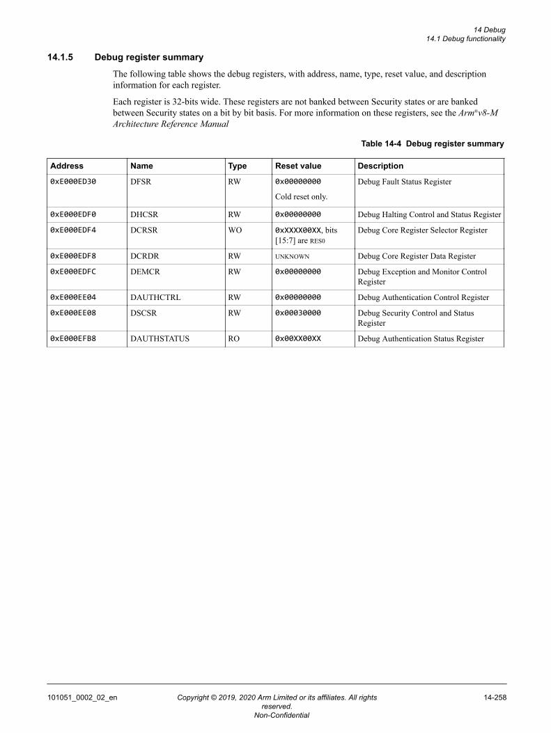
14.1.5 Debug register summary
The following table shows the debug registers, with address, name, type, reset value, and descriptioninformation for each register.
Each register is 32-bits wide. These registers are not banked between Security states or are bankedbetween Security states on a bit by bit basis. For more information on these registers, see the Arm®v8-MArchitecture Reference Manual
Table 14-4 Debug register summary
Address Name Type Reset value Description
0xE000ED30 DFSR RW 0x00000000
Cold reset only.
Debug Fault Status Register
0xE000EDF0 DHCSR RW 0x00000000 Debug Halting Control and Status Register
0xE000EDF4 DCRSR WO 0xXXXX00XX, bits[15:7] are RES0
Debug Core Register Selector Register
0xE000EDF8 DCRDR RW UNKNOWN Debug Core Register Data Register
0xE000EDFC DEMCR RW 0x00000000 Debug Exception and Monitor ControlRegister
0xE000EE04 DAUTHCTRL RW 0x00000000 Debug Authentication Control Register
0xE000EE08 DSCSR RW 0x00030000 Debug Security Control and StatusRegister
0xE000EFB8 DAUTHSTATUS RO 0x00XX00XX Debug Authentication Status Register
14 Debug14.1 Debug functionality
101051_0002_02_en Copyright © 2019, 2020 Arm Limited or its affiliates. All rightsreserved.
14-258
Non-Confidential
14.2 D-AHB interfaceThe 32-bit Debug AHB (D-AHB) interface implements the AMBA 5 AHB protocol. It can be used with aCoreSight AHB-AP to provide debugger access to all processor control and debug resources, and a viewof memory that is consistent with that observed by load and store operations.
Accesses on the D-AHB interface are always little-endian.
Debugger accesses are distributed to the appropriate internal and external resource according to theaddress of the request. Accesses on the D-AHB are reflected on the TCM, Master AXI (M-AXI),Peripheral AHB (P-AHB), and External Private Peripheral Bus (EPPB) as appropriate.
14.2.1 Debug memory access
The Cortex-M55 processor implements external debug interaction through a 32-bit AMBA 5 AHB debuginterface.
This interface can be integrated with a suitable CoreSight AHB-AP interface and provides debuggeraccess to:
• All processor control and debug resources.• A view of memory, which is consistent with the view that software load and store operations observe.
Accesses on the D-AHB interface always ignore the endianness attribute and do not pass through thedata swizzling logic in the processor used for load and store requests. Therefore, accesses to addressesoutside the PPB region observe data in the downstream memory endian format and accesses in the PPBregion observe data in little-endian format.• Debug AHB (D-AHB) accesses undergo security attribution and security access checks. The debug
Security state depends on DHCSR.S_SDE and the D-AHB input signal, HNONSECD, whichindicates the security level that a debug access requests. If this signal is asserted, this indicates thatthe transfer is Non-secure.
• D-AHB accesses are not checked against the Memory Protection Unit (MPU) for memory attributechecks unless the Unprivileged Debug is enabled for a debug Security state.— Unprivileged Debug is enabled for the secure debug state when DHCSR.S_SUIDE is set.— Unprivileged Debug is enabled for the Non-secure debug state when DHCSR.S_NSUIDE is set.
• If unprivileged debug is enabled, then the access is always treated as unprivileged, regardless of thevalue of the D-AHB signal bit HPROTD[1] and reported on the D-AHB interface.— If the debug Security state is Secure, then the D-AHB access is subject to permission checks
based on regions that are defined in the Secure MPU.— If the debug Security state is Non-secure, then the D-AHB access is subject to permission checks
based on regions that are defined in the Non-secure MPU.• D-AHB accesses to the EPPB memory region (0xE0040000-0xE00FEFFF) must be marked as
privileged, HPROT[1] HIGH, unless unprivileged invasive Debug Access Port (DAP) access isenabled by setting DAUTHCTRL.UIDAPEN for the debug security state. WhenDAUTHCTRL.UIDAPEN is set all the peripherals in the EPPB region can be accessed by non-privileged debug accesses through D-AHB except for the:— External Wakeup Interrupt Controller (EWIC) located at 0xE0047000-0xE0047FFF.— Reserved regions at 0xE0046000-0xE0046FFF and 0xE0048000-0xE0048FFF
These regions can only be accessed with Secure privileged requests. Any non-privileged accessesreturns an error on D-AHB.
• D-AHB accesses to the internal PPB region must be marked as privileged, unless unprivilegedinvasive DAP access is enabled by setting DAUTHCTRL.UIDAPEN for the debug Security state.— When DAUTHCTRL.UIDAPEN is set, many of the registers in the internal PPB region can be
accessed. The exceptions are those registers which are normally accessible by unprivileged code.For example, some of the Instrumentation Trace Macrocell (ITM) registers and the STIR. For
14 Debug14.2 D-AHB interface
101051_0002_02_en Copyright © 2019, 2020 Arm Limited or its affiliates. All rightsreserved.
14-259
Non-Confidential
more information on the ITM registers, see 16.2 ITM register summary on page 16-277. For moreinformation on STIR, see Arm®v8-M Architecture Reference Manual.
— When DAUTHCTRL.UIDAPEN is not set and the debug access is unprivileged, then almost allaccesses to the PPB registers get an error response. However, the registers which are normallyaccessible by unprivileged code cannot be accessed. For example, some of the InstrumentationTrace Macrocell (ITM) registers and the STIR. For more information on the ITM registers, see16.2 ITM register summary on page 16-277. For more information on STIR, see Arm®v8-MArchitecture Reference Manual.
• The security of a debug transaction on one of the external interfaces is determined by all of thefollowing:— The access control signals.— The mapping of the address in the Security Attribution Unit (SAU) and Implementation Defined
Attribution Unit (IDAU).— The internal debug state of the processor.— The HNONSECD signal value that is associated with the D-AHB debug request.
Note
• For more information on the DHCSR and DAUTHCTRL registers, see the Arm®v8-M ArchitectureReference Manual.
• For more information on all the AMBA 5 AHB-compliant D-AHB signals mentioned in this section,see the Arm® AMBA® 5 AHB Protocol Specification.
14.2.2 Debugger access memory attributes and data cache access
The memory attributes associated with debugger accesses on Debug AHB (D-AHB) depend on the debugaccess mode.
Unprivileged Debug is not enabled
If Unprivileged Debug is not enabled, debugger accesses are not subject to the memory attributes definedby the Memory Protection Unit (MPU). Instead, the memory attributes used to perform a debuggeraccess are derived from the HPROTD signal on D-AHB. The attributes are used differently dependingon the memory region that is associated with the address.
The following table shows the behavior of debug accesses and dependency on HPROTD for bothinternal and externally memory-mapped regions when Unprivileged Debug is not enabled.
14 Debug14.2 D-AHB interface
101051_0002_02_en Copyright © 2019, 2020 Arm Limited or its affiliates. All rightsreserved.
14-260
Non-Confidential
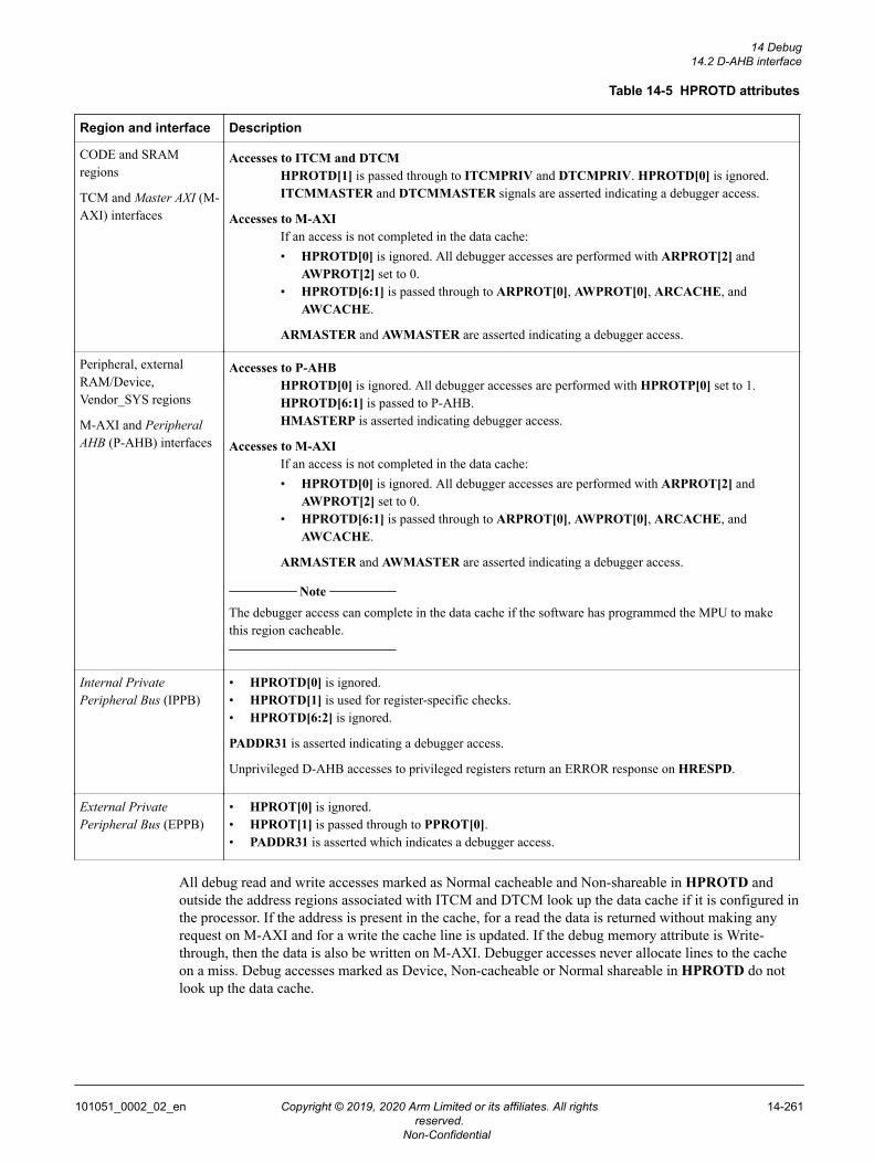
Table 14-5 HPROTD attributes
Region and interface Description
CODE and SRAMregions
TCM and Master AXI (M-AXI) interfaces
Accesses to ITCM and DTCMHPROTD[1] is passed through to ITCMPRIV and DTCMPRIV. HPROTD[0] is ignored.ITCMMASTER and DTCMMASTER signals are asserted indicating a debugger access.
Accesses to M-AXIIf an access is not completed in the data cache:• HPROTD[0] is ignored. All debugger accesses are performed with ARPROT[2] and
AWPROT[2] set to 0.• HPROTD[6:1] is passed through to ARPROT[0], AWPROT[0], ARCACHE, and
AWCACHE.
ARMASTER and AWMASTER are asserted indicating a debugger access.
Peripheral, externalRAM/Device,Vendor_SYS regions
M-AXI and PeripheralAHB (P-AHB) interfaces
Accesses to P-AHBHPROTD[0] is ignored. All debugger accesses are performed with HPROTP[0] set to 1.HPROTD[6:1] is passed to P-AHB.HMASTERP is asserted indicating debugger access.
Accesses to M-AXIIf an access is not completed in the data cache:• HPROTD[0] is ignored. All debugger accesses are performed with ARPROT[2] and
AWPROT[2] set to 0.• HPROTD[6:1] is passed through to ARPROT[0], AWPROT[0], ARCACHE, and
AWCACHE.
ARMASTER and AWMASTER are asserted indicating a debugger access.
Note
The debugger access can complete in the data cache if the software has programmed the MPU to makethis region cacheable.
Internal PrivatePeripheral Bus (IPPB)
• HPROTD[0] is ignored.• HPROTD[1] is used for register-specific checks.• HPROTD[6:2] is ignored.
PADDR31 is asserted indicating a debugger access.
Unprivileged D-AHB accesses to privileged registers return an ERROR response on HRESPD.
External PrivatePeripheral Bus (EPPB)
• HPROT[0] is ignored.• HPROT[1] is passed through to PPROT[0].• PADDR31 is asserted which indicates a debugger access.
All debug read and write accesses marked as Normal cacheable and Non-shareable in HPROTD andoutside the address regions associated with ITCM and DTCM look up the data cache if it is configured inthe processor. If the address is present in the cache, for a read the data is returned without making anyrequest on M-AXI and for a write the cache line is updated. If the debug memory attribute is Write-through, then the data is also be written on M-AXI. Debugger accesses never allocate lines to the cacheon a miss. Debug accesses marked as Device, Non-cacheable or Normal shareable in HPROTD do notlook up the data cache.
14 Debug14.2 D-AHB interface
101051_0002_02_en Copyright © 2019, 2020 Arm Limited or its affiliates. All rightsreserved.
14-261
Non-Confidential
Unprivileged Debug is enabled
If Unprivileged Debug is enabled, the Memory Protection Unit (MPU) determines whether an access isallowed according to the privilege set in HPROTD[1] and the memory attributes associated with thememory access. The value HPROTD[6:2] is ignored.
Table 14-6 Memory attributes
Region and interface Description
CODE and SRAM regions
TCM and Master AXI (M-AXI) interfaces
Accesses to ITCM and DTCMHPROTD[1] is passed through to ITCMPRIV and DTCMPRIV.ITCMMASTER and DTCMMASTER signals have been asserted indicating a debuggeraccess.
Accesses to M-AXIIf an access is not completed in the data cache:• All debugger accesses are performed with ARPROT[2] and AWPROT[2] set to 0.• The memory attributes are passed through to ARPROT[0], AWPROT[0], ARCACHE,
and AWCACHE.
ARMASTER and AWMASTER are asserted indicating a debugger access.
Peripheral, external RAM/Device, Vendor_SYS regions
M-AXI and Peripheral AHB(P-AHB) interfaces
Accesses to P-AHBAll debugger accesses are performed with HPROTP[0] set to 1.The memory attributes are passed to P-AHB.HMASTERP is asserted indicating debugger access.
Accesses to M-AXIIf an access is not completed in the data cache:• All debugger accesses are performed with ARPROT[2] and AWPROT[2] set to 0.• The memory attributes are passed through to ARPROT[0], AWPROT[0], ARCACHE,
and AWCACHE.
ARMASTER and AWMASTER are asserted indicating a debugger access.
Internal Private PeripheralBus (IPPB)
PADDR31 is asserted indicating a debugger access.
Unprivileged access in some registers is allowed when DAUTHCTRL.UIDAPEN is set. ifUnprivileged access is not allowed, an error response is returned on HRESPD.
External Private PeripheralBus (EPPB)
PADDR31 is asserted which indicates a debugger access.
14.2.3 Debug access security and attributes
Debugger accesses to memory and any memory-mapped registers are subject to the same security checksas data accesses generated by software running on the processor, with the security attributes set as thefollowing:
• Request is Secure if the DHCSR.S_SDE register field is 1 indicating secure debug is enabled andHNONSECD is LOW.
• Otherwise the request is Non-secure.
The state of DHCSR.S_SDE depends on the context of the debug request. If the processor is halted whenit was in Secure state, then DHCSR.S_SDE is 1, otherwise the value of the field depends on the secureaccess control input signal. This implies access to the secure state and memory is only available if secureinvasive debug is permitted in the system.
In most of the memory regions, debugger accesses are subject to validation and attribution. This impliesthat the final security state of an access on the Master AXI (M-AXI), Peripheral AHB (P-AHB), and
14 Debug14.2 D-AHB interface
101051_0002_02_en Copyright © 2019, 2020 Arm Limited or its affiliates. All rightsreserved.
14-262
Non-Confidential
External Private Peripheral Bus (EPPB) interfaces are set by the Security Attribution Unit (SAU) in thesame way as software generated accesses. The SAU blocks memory accesses which do not have therequired permissions. For example, accesses to memory regions marked as Secure in the SAU ifDHCSR.S_SDE is 0 or HNONSECD is HIGH. This results in an error response on the Debug AHB (D-AHB) interface, but unlike accesses originating from software, a SecureFault is not raised.
There are a number of address regions associated with the System Control Space (SCS) and debugperipherals where the security state of the access is determined only by the HNONSECD signal andDHCSR.S_SDE. For more information on these address regions, see 8.5 Memory regions not controlledby SAU and IDAU on page 8-162.
If the security extensions are not included in the processor, DHCSR.S_SDE behaves as RAZ/WI,therefore all debug accesses are considered to be Non-secure.
Note
For more information on the DHCSR register, see the Arm®v8-M Architecture Reference Manual. Formore information on all the AMBA 5 AHB-compliant HNONSECD signal, see the Arm® AMBA® 5 AHBProtocol Specification.
14.2.4 Debug during reset and before code execution commences
The Cortex-M55 processor supports access to the debug and trace resource from a debug agentconnected to the Debug AHB (D-AHB) interface when the device is in processor reset. This can be usefulfor setting up the debug and trace environment before any code has executed on the processor.
The following table lists the memory regions which can be accessed during processor reset. Accesscontrol and security level are determined in the same manner as debug accesses during code execution orwhen halted based on the authentication signals and the default SAU/IDAU regions. Any component onthe EPPB, which cannot be accessed during reset, must ensure the APB PREADY and PSLVERRsignals are HIGH in response to a request from the processor.
Access to all other memory areas during processor reset is UNPREDICTABLE.
Table 14-7 Debug and trace registers accessible during processor reset
Memory address range Group Description
0xE000E000-0xE000E00F System Control and ID registers Includes the ICTR and ACTLR registers. For more information onthe ICTR register, see the Arm®v8-M Architecture Reference Manualand for more information on the ACTLR register, see 4.8 ACTLR,Auxiliary Control Register on page 4-68.
0xE000ED00-0xE000ED8F System Control Block (SCB) registers. For more information, see theArm®v8-M Architecture Reference Manual.
0xE000EDF0-0xE000EEFF Debug registers in the System Control Space (SCS). For moreinformation, see the Arm®v8-M Architecture Reference Manual.
0xE000EF00-0xE000EF8F Includes the STIR register. For more information, see the Arm®v8-MArchitecture Reference Manual.
0xE000E010-0xE00E01F SysTick Timer SysTick Timer registers. For more information, see the Arm®v8-MArchitecture Reference Manual.
0xE000E100-0xE000E7BF Nested Vectored InterruptController (NVIC)
11.3 NVIC register summary on page 11-234
0xE0000000-0xE0000FFF Instrumentation Trace Macrocell(ITM)
16.2 ITM register summary on page 16-277
14 Debug14.2 D-AHB interface
101051_0002_02_en Copyright © 2019, 2020 Arm Limited or its affiliates. All rightsreserved.
14-263
Non-Confidential
Table 14-7 Debug and trace registers accessible during processor reset (continued)
Memory address range Group Description
0xE0001000-0xE0001FFF Data Watchpoint and Trace(DWT)
17.5 DWT register summary on page 17-290
0xE0002000-0xE0002FFF Breakpoint Unit (BPU) 19.2 BPU register summary on page 19-334
0xE0003000-0xE0003FFF Performance Monitoring Unit(PMU)
Chapter 15 Performance Monitoring Unit Extension on page 15-265
0xE0041000-0xE0041FFF Embedded Trace Macrocell(ETM)
For more information, see the Arm® CoreSight™ ETM‑M55 TechnicalReference Manual
0xE0042000-0xE0042FFF Cross Trigger Interface (CTI) 18.2 CTI register summary on page 18-296
0xE0046000-0xE0046FFF Reserved -
0xE0044000-0xE00FFFFF External Private Peripheral Bus(EPPB)
Access directed to Cortex-M55 EPPB APB interface.
14.2.5 Advanced DSP debug capabilities
The Cortex-M55 processor supports the Digital Signal Processing (DSP) Debug Extension to provideadditional features for analyzing signal processing and compute software using the Data Watchpoint andTrace (DWT) and Performance Monitoring Unit (PMU).
For more information on the DSP Debug Extension, see the Arm®v8-M Architecture Reference Manualand include the following additional functionality to the processor.
The DSP debug capabilities supported are:
DWT value mask
Value matching using the DWT comparators, DWT_COMPn, is extended to use a mask registerDWT_VMASKn. This allows events to be selected based on sub-word values or arbitrarybitfields. This is useful for analyzing data where only part of the data word is valid.
Halt request on PMU overflow
The processor can be configured to enter debug Halt when a PMU counter, which is configuredto generate an interrupt overflow. This can be used to set up a hardware watchpoint which istriggered after a number of events have been observed in a system.
Extended PMU events
The DSP Debug Extension defines additional PMU events specific to M-profile debug and traceoperation TRCEXTOUT, CTI_TRIGOUT and DWT_CMPMATCH. For more information onthese events, see 15.2 PMU events on page 15-267.
14 Debug14.2 D-AHB interface
101051_0002_02_en Copyright © 2019, 2020 Arm Limited or its affiliates. All rightsreserved.
14-264
Non-Confidential
Chapter 15Performance Monitoring Unit Extension
This chapter describes the Performance Monitoring Unit (PMU) Extension.
It contains the following sections:• 15.1 PMU features on page 15-266.• 15.2 PMU events on page 15-267.• 15.3 PMU register summary on page 15-272.
101051_0002_02_en Copyright © 2019, 2020 Arm Limited or its affiliates. All rightsreserved.
15-265
Non-Confidential
15.1 PMU featuresThe Cortex-M55 processor Data Watchpoint and Trace (DWT) implements the Performance MonitoringUnit (PMU). This enables software to get information about events that are taking place in the processorand can be used for performance analysis and system debug.
The PMU supports eight 16-bit event counters and one 32-bit cycle counter. Each event counter cancount one event from a list comprising both architectural and IMPLEMENTATION DEFINED events. For moreinformation on PMU events, see 15.2 PMU events on page 15-267. The PMU also supports a chainfunction which allows the PMU to cascade two of the 16-bit counters into one 32-bit counter. Only oddevent counters support the chain feature. PMU counters increment if the appropriate bit inPMU_CNTENSET register is set.
The Armv8.1‑M architecture specifies that operation of the PMU counters and DWT profiling countersis mutually exclusive. The Cortex-M55 processor uses this requirement to share the state used for thecounters.
The PMU cycle counter PMU_CCNTR is an alias of the DWT_CYCCNT register. All derived functionsof the counter are available whenever either the DWT or the PMU enables the cycle counter. If the DWTis included in the processor, DWT_CTRL.NOCYCCNT is RAZ.
Generating interrupts
If a counter is configured to generate an interrupt when it overflows, DEMCR.MON_PEND is set to 1 tomake a Debug Monitor exception pended with DFSR.PMU set to 1. The associated overflow bitprogrammed by PMU_OVSSET and PMU_OVSCLR indicates which counter triggered the exception.The interrupts are enabled if their corresponding bit programmed by PMU_INTENSET andPMU_INTENCLR is set and DEMCR.MON_EN is 1.
Exporting trace
The PMU can export trace whenever the lower 8 bits of the counters overflow. The PMU issues an eventcounter packet with the appropriate counter flag set to 1. This occurs on counter increment only, not onsoftware or debugger write. For each counter n, if the lower 8 bits of that counter overflows, theassociated OVn bit of the event counter packet is set. If multiple counters overflow during the sameperiod, multiple bits might be set.
The PMU can serve as an event source for the Cross Trigger Interface (CTI).
For more information on the registers mentioned in this section, see the Arm®v8-M ArchitectureReference Manual.
Note
The Performance Monitoring Unit (PMU) is included if the Data Watchpoint and Trace (DWT) isincluded in the processor. For more information on performance monitoring, see the Arm®v8.1‑MPerformance Monitoring User Guide Application Note.
15 Performance Monitoring Unit Extension15.1 PMU features
101051_0002_02_en Copyright © 2019, 2020 Arm Limited or its affiliates. All rightsreserved.
15-266
Non-Confidential
15.2 PMU eventsThe following table shows the events that are generated and the numbers that the PerformanceMonitoring Unit (PMU) uses to reference the events.
Table 15-1 PMU events
Eventnumber
Event mnemonic PMUeventbus bit
Event name
0x0000 SW_INCR 0 Instruction architecturally executed, conditioncode check pass, software increment
0x0001 L1I_CACHE_REFILL 1 L1 instruction cache linefill
0x0003 L1D_CACHE_REFILL 2 L1 data cache linefill
0x0004 L1D_CACHE 3 L1 data cache access
0x0006 LD_RETIRED 4 Instruction architecturally executed, conditioncode check pass, load
0x0007 ST_RETIRED 5 Instruction architecturally executed, conditioncode check pass, store
0x0008 INST_RETIRED 6 Instruction architecturally executed.
0x0009 EXC_TAKEN 7 Exception taken.
0x000A EXC_RETURN 8 Instruction architecturally executed, conditioncode check pass, exception return.
0x000C PC_WRITE_RETIRED 9 Instruction architecturally executed, conditioncode check pass, software change of the PC.
0x000D BR_IMMED_RETIRED 10 Instruction architecturally executed, immediatebranch.
0x000E BR_RETURN_RETIRED 11 Instruction architecturally executed, conditioncode check pass, procedure return.
0x000F UNALIGNED_LDST_RETIRED 12 Instruction architecturally executed, conditioncode check pass, unaligned load or store.
0x0011 CPU_CYCLES 14 Cycle.
0x0013 MEM_ACCESS 16 Data memory access.
0x0014 L1I_CACHE 17 L1 instruction cache access.
0x0015 L1D_CACHE_WB 18 L1 data cache write-back
0x0019 BUS_ACCESS 19 Any beat access to the M-AXI read interface, M-AXI write interface and any access to P-AHBinterface
0x001A MEMORY_ERROR 20 ECC error for TCMs and caches.
0x001D BUS_CYCLES 22 Counts the number of cycles on which the M-AXI interface is clocked.
15 Performance Monitoring Unit Extension15.2 PMU events
101051_0002_02_en Copyright © 2019, 2020 Arm Limited or its affiliates. All rightsreserved.
15-267
Non-Confidential
Table 15-1 PMU events (continued)
Eventnumber
Event mnemonic PMUeventbus bit
Event name
0x001E CHAIN 23 For an odd-numbered counter, increments whenan overflow occurs on the preceding even-numbered counter on the same PE.
0x0021 BR_RETIRED 25 Instruction architecturally executed, branch.
0x0022 BR_MIS_PRED_RETIRED 26 Instruction architecturally executed,mispredicted branch.
0x0023 STALL_FRONTEND 27 If there are no instructions available from thefetch stage of the processor pipeline, theprocessor considers the front-end of theprocessor pipeline as being stalled.
0x0024 STALL_BACKEND 28 If there is an instruction available from the fetchstage of the pipeline but it cannot be accepted bythe decode stage of the processor pipeline, theprocessor considers the back-end of theprocessor pipeline as being stalled.
0x0036 LL_CACHE_RD 29 L1 data cache read. For the Cortex-M55processor, this event is the same asL1_CACHE_RD.
0x0037 LL_CACHE_MISS_RD 30 L1 data cache read miss. For the Cortex-M55processor, this event is the same asL1D_CACHE_MISS_RD.
0x0039 L1D_CACHE_MISS_RD 31 L1 data cache read miss. For the Cortex-M55processor, this event is the same asLL_CACHE_MISS_RD.
0x003C STALL 34 No operation sent for execution.
0x0040 L1D_CACHE_RD 38 L1 data cache read. For the Cortex-M55processor, this event is the same asLL_CACHE_RD.
0x0100 LE_RETIRED 39 Loop end instruction architecturally executed,entry registered in the LO_BRANCH_INFOcache.
0x0108 LE_CANCEL 43 LO_BRANCH_INFO cache containing a validloop entry cleared while not in the last iterationof the loop.
0x0114 SE_CALL_S 45 Call to secure function, resulting in security statechange.
0x0115 SE_CALL_NS 46 Call to Non-secure function, resulting in securitystate change
0x0118 DWT_CMPMATCH0 47 Data Watchpoint and Trace (DWT) comparator 0match
15 Performance Monitoring Unit Extension15.2 PMU events
101051_0002_02_en Copyright © 2019, 2020 Arm Limited or its affiliates. All rightsreserved.
15-268
Non-Confidential
Table 15-1 PMU events (continued)
Eventnumber
Event mnemonic PMUeventbus bit
Event name
0x0119 DWT_CMPMATCH1 48 DWT comparator 1 match
0x011A DWT_CMPMATCH2 49 DWT comparator 2 match
0x011B DWT_CMPMATCH3 50 DWT comparator 3 match
0x0200 MVE_INST_RETIRED 51 M‑profile Vector Extension (MVE) instructionarchitecturally executed
0x0204 MVE_FP_RETIRED 53 MVE floating-point instruction architecturallyexecuted.
0x0208 MVE_FP_HP_RETIRED 55 MVE half-precision floating-point instructionarchitecturally executed
0x020C MVE_FP_SP_RETIRED 57 MVE single-precision floating-point instructionarchitecturally executed
0x0214 MVE_FP_MAC_RETIRED 59 MVE floating-point multiply or multiplyaccumulate instruction architecturally executed
0x0224 MVE_INT_RETIRED 61 MVE integer instruction architecturally executed
0x0228 MVE_INT_MAC_RETIRED 63 MVE integer multiply or multiply-accumulateinstruction architecturally executed
0x0238 MVE_LDST_RETIRED 65 MVE load or store instruction architecturallyexecuted
0x023C MVE_LD_RETIRED 67 MVE load instruction architecturally executed
0x0240 MVE_ST_RETIRED 69 MVE store instruction architecturally executed
0x0244 MVE_LDST_CONTIG_RETIRED 71 MVE contiguous load or store instructionarchitecturally executed
0x0248 MVE_LD_CONTIG_RETIRED 73 MVE contiguous load instruction architecturallyexecuted
0x024C MVE_ST_CONTIG_RETIRED 75 MVE contiguous store instruction architecturallyexecuted
0x0250 MVE_LDST_NONCONTIG_RETIRED 77 MVE non-contiguous load or store instructionarchitecturally executed
0x0254 MVE_LD_NONCONTIG_RETIRED 79 MVE non-contiguous load instructionarchitecturally executed
0x0258 MVE_ST_NONCONTIG_RETIRED 81 MVE non-contiguous store instructionarchitecturally executed
0x025C MVE_LDST_MULTI_RETIRED 83 MVE memory instruction targeting multipleregisters architecturally executed
0x0260 MVE_LD_MULTI_RETIRED 85 MVE memory load instruction targeting multipleregisters architecturally executed
0x0264 MVE_ST_MULTI_RETIRED 87 MVE memory store instruction targetingmultiple registers architecturally executed
15 Performance Monitoring Unit Extension15.2 PMU events
101051_0002_02_en Copyright © 2019, 2020 Arm Limited or its affiliates. All rightsreserved.
15-269
Non-Confidential
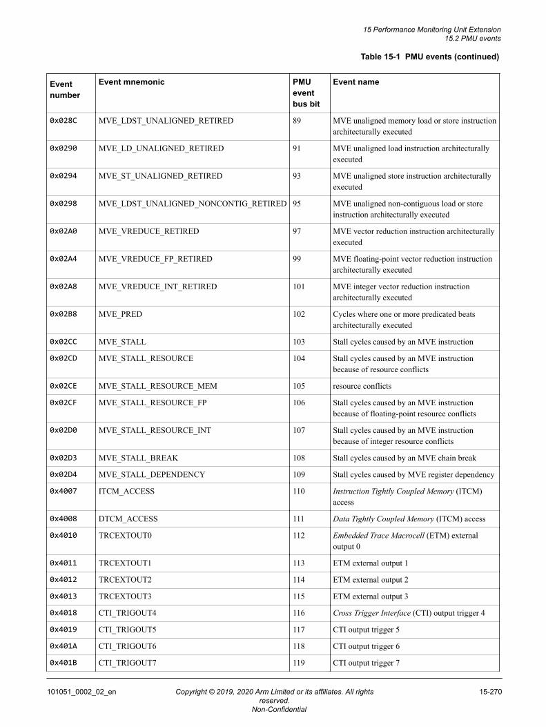
Table 15-1 PMU events (continued)
Eventnumber
Event mnemonic PMUeventbus bit
Event name
0x028C MVE_LDST_UNALIGNED_RETIRED 89 MVE unaligned memory load or store instructionarchitecturally executed
0x0290 MVE_LD_UNALIGNED_RETIRED 91 MVE unaligned load instruction architecturallyexecuted
0x0294 MVE_ST_UNALIGNED_RETIRED 93 MVE unaligned store instruction architecturallyexecuted
0x0298 MVE_LDST_UNALIGNED_NONCONTIG_RETIRED 95 MVE unaligned non-contiguous load or storeinstruction architecturally executed
0x02A0 MVE_VREDUCE_RETIRED 97 MVE vector reduction instruction architecturallyexecuted
0x02A4 MVE_VREDUCE_FP_RETIRED 99 MVE floating-point vector reduction instructionarchitecturally executed
0x02A8 MVE_VREDUCE_INT_RETIRED 101 MVE integer vector reduction instructionarchitecturally executed
0x02B8 MVE_PRED 102 Cycles where one or more predicated beatsarchitecturally executed
0x02CC MVE_STALL 103 Stall cycles caused by an MVE instruction
0x02CD MVE_STALL_RESOURCE 104 Stall cycles caused by an MVE instructionbecause of resource conflicts
0x02CE MVE_STALL_RESOURCE_MEM 105 resource conflicts
0x02CF MVE_STALL_RESOURCE_FP 106 Stall cycles caused by an MVE instructionbecause of floating-point resource conflicts
0x02D0 MVE_STALL_RESOURCE_INT 107 Stall cycles caused by an MVE instructionbecause of integer resource conflicts
0x02D3 MVE_STALL_BREAK 108 Stall cycles caused by an MVE chain break
0x02D4 MVE_STALL_DEPENDENCY 109 Stall cycles caused by MVE register dependency
0x4007 ITCM_ACCESS 110 Instruction Tightly Coupled Memory (ITCM)access
0x4008 DTCM_ACCESS 111 Data Tightly Coupled Memory (ITCM) access
0x4010 TRCEXTOUT0 112 Embedded Trace Macrocell (ETM) externaloutput 0
0x4011 TRCEXTOUT1 113 ETM external output 1
0x4012 TRCEXTOUT2 114 ETM external output 2
0x4013 TRCEXTOUT3 115 ETM external output 3
0x4018 CTI_TRIGOUT4 116 Cross Trigger Interface (CTI) output trigger 4
0x4019 CTI_TRIGOUT5 117 CTI output trigger 5
0x401A CTI_TRIGOUT6 118 CTI output trigger 6
0x401B CTI_TRIGOUT7 119 CTI output trigger 7
15 Performance Monitoring Unit Extension15.2 PMU events
101051_0002_02_en Copyright © 2019, 2020 Arm Limited or its affiliates. All rightsreserved.
15-270
Non-Confidential
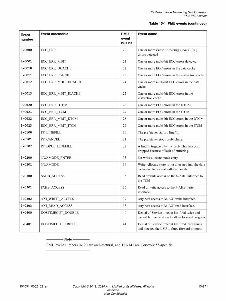
Table 15-1 PMU events (continued)
Eventnumber
Event mnemonic PMUeventbus bit
Event name
0xC000 ECC_ERR 120 One or more Error Correcting Code (ECC)errors detected
0xC001 ECC_ERR_MBIT 121 One or more multi-bit ECC errors detected
0xC010 ECC_ERR_DCACHE 122 One or more ECC errors in the data cache
0xC011 ECC_ERR_ICACHE 123 One or more ECC errors in the instruction cache
0xC012 ECC_ERR_MBIT_DCACHE 124 One or more multi-bit ECC errors in the datacache
0xC013 ECC_ERR_MBIT_ICACHE 125 One or more multi-bit ECC errors in theinstruction cache
0xC020 ECC_ERR_DTCM 126 One or more ECC errors in the DTCM
0xC021 ECC_ERR_ITCM 127 One or more ECC errors in the ITCM
0xC022 ECC_ERR_MBIT_DTCM 128 One or more multi-bit ECC errors in the DTCM
0xC023 ECC_ERR_MBIT_ITCM 129 One or more multi-bit ECC errors in the ITCM
0xC100 PF_LINEFILL 130 The prefetcher starts a linefill.
0xC101 PF_CANCEL 131 The prefetcher stops prefetching.
0xC102 PF_DROP_LINEFILL 132 A linefill triggered by the prefetcher has beendropped because of lack of buffering.
0xC200 NWAMODE_ENTER 133 No-write allocate mode entry
0xC201 NWAMODE 134 Write-Allocate store is not allocated into the datacache due to no-write-allocate mode
0xC300 SAHB_ACCESS 135 Read or write access on the S-AHB interface tothe TCM
0xC301 PAHB_ACCESS 136 Read or write access to the P-AHB writeinterface
0xC302 AXI_WRITE_ACCESS 137 Any beat access to M-AXI write interface.
0xC303 AXI_READ_ACCESS 138 Any beat access to M-AXI read interface.
0xC400 DOSTIMEOUT_DOUBLE 140 Denial of Service timeout has fired twice andcaused buffers to drain to allow forward progress
0xC401 DOSTIMEOUT_TRIPLE 141 Denial of Service timeout has fired three timesand blocked the LSU to force forward progress
Note
PMU event numbers 0-120 are architectural, and 121-141 are Cortex-M55-specific.
15 Performance Monitoring Unit Extension15.2 PMU events
101051_0002_02_en Copyright © 2019, 2020 Arm Limited or its affiliates. All rightsreserved.
15-271
Non-Confidential
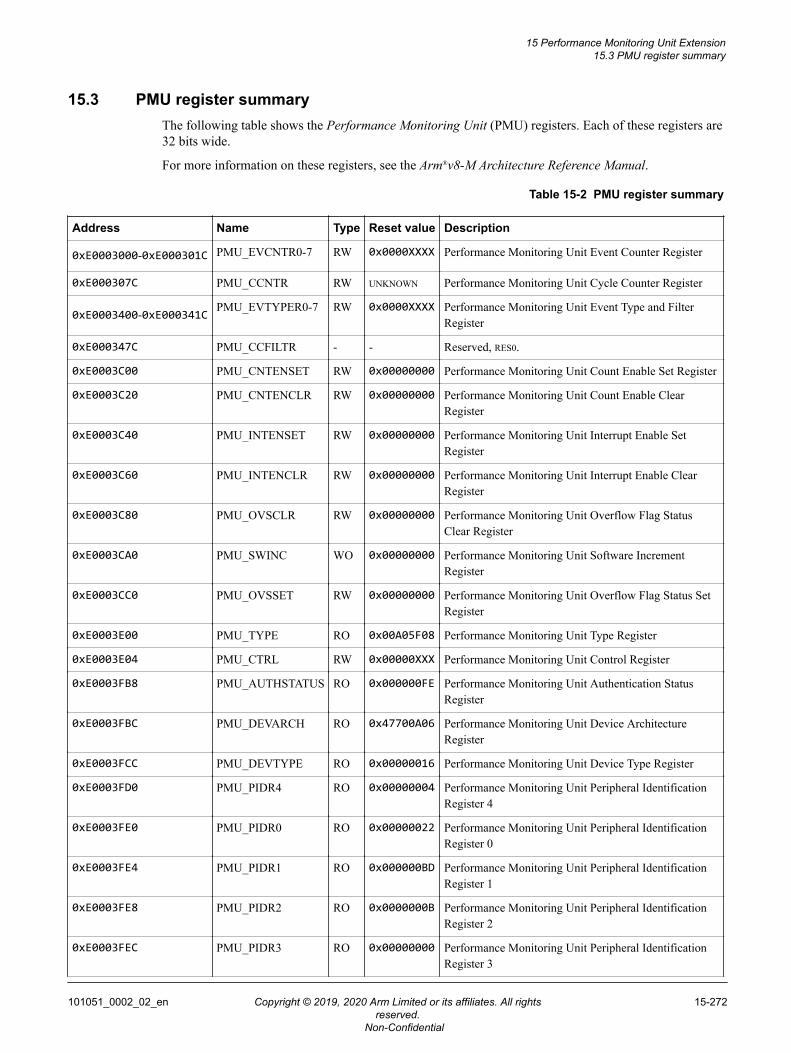
15.3 PMU register summaryThe following table shows the Performance Monitoring Unit (PMU) registers. Each of these registers are32 bits wide.
For more information on these registers, see the Arm®v8-M Architecture Reference Manual.
Table 15-2 PMU register summary
Address Name Type Reset value Description
0xE0003000-0xE000301C PMU_EVCNTR0-7 RW 0x0000XXXX Performance Monitoring Unit Event Counter Register
0xE000307C PMU_CCNTR RW UNKNOWN Performance Monitoring Unit Cycle Counter Register
0xE0003400-0xE000341C PMU_EVTYPER0-7 RW 0x0000XXXX Performance Monitoring Unit Event Type and FilterRegister
0xE000347C PMU_CCFILTR - - Reserved, RES0.
0xE0003C00 PMU_CNTENSET RW 0x00000000 Performance Monitoring Unit Count Enable Set Register
0xE0003C20 PMU_CNTENCLR RW 0x00000000 Performance Monitoring Unit Count Enable ClearRegister
0xE0003C40 PMU_INTENSET RW 0x00000000 Performance Monitoring Unit Interrupt Enable SetRegister
0xE0003C60 PMU_INTENCLR RW 0x00000000 Performance Monitoring Unit Interrupt Enable ClearRegister
0xE0003C80 PMU_OVSCLR RW 0x00000000 Performance Monitoring Unit Overflow Flag StatusClear Register
0xE0003CA0 PMU_SWINC WO 0x00000000 Performance Monitoring Unit Software IncrementRegister
0xE0003CC0 PMU_OVSSET RW 0x00000000 Performance Monitoring Unit Overflow Flag Status SetRegister
0xE0003E00 PMU_TYPE RO 0x00A05F08 Performance Monitoring Unit Type Register
0xE0003E04 PMU_CTRL RW 0x00000XXX Performance Monitoring Unit Control Register
0xE0003FB8 PMU_AUTHSTATUS RO 0x000000FE Performance Monitoring Unit Authentication StatusRegister
0xE0003FBC PMU_DEVARCH RO 0x47700A06 Performance Monitoring Unit Device ArchitectureRegister
0xE0003FCC PMU_DEVTYPE RO 0x00000016 Performance Monitoring Unit Device Type Register
0xE0003FD0 PMU_PIDR4 RO 0x00000004 Performance Monitoring Unit Peripheral IdentificationRegister 4
0xE0003FE0 PMU_PIDR0 RO 0x00000022 Performance Monitoring Unit Peripheral IdentificationRegister 0
0xE0003FE4 PMU_PIDR1 RO 0x000000BD Performance Monitoring Unit Peripheral IdentificationRegister 1
0xE0003FE8 PMU_PIDR2 RO 0x0000000B Performance Monitoring Unit Peripheral IdentificationRegister 2
0xE0003FEC PMU_PIDR3 RO 0x00000000 Performance Monitoring Unit Peripheral IdentificationRegister 3
15 Performance Monitoring Unit Extension15.3 PMU register summary
101051_0002_02_en Copyright © 2019, 2020 Arm Limited or its affiliates. All rightsreserved.
15-272
Non-Confidential
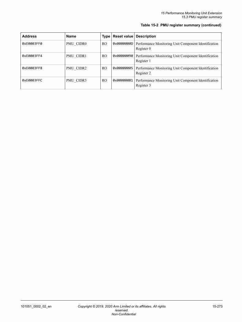
Table 15-2 PMU register summary (continued)
Address Name Type Reset value Description
0xE0003FF0 PMU_CIDR0 RO 0x0000000D Performance Monitoring Unit Component IdentificationRegister 0
0xE0003FF4 PMU_CIDR1 RO 0x00000090 Performance Monitoring Unit Component IdentificationRegister 1
0xE0003FF8 PMU_CIDR2 RO 0x00000005 Performance Monitoring Unit Component IdentificationRegister 2
0xE0003FFC PMU_CIDR3 RO 0x000000B1 Performance Monitoring Unit Component IdentificationRegister 3
15 Performance Monitoring Unit Extension15.3 PMU register summary
101051_0002_02_en Copyright © 2019, 2020 Arm Limited or its affiliates. All rightsreserved.
15-273
Non-Confidential
Chapter 16Instrumentation Trace Macrocell
This chapter describes the Instrumentation Trace Macrocell (ITM).
It contains the following sections:• 16.1 ITM features on page 16-275.• 16.2 ITM register summary on page 16-277.• 16.3 ITM_TPR, ITM Trace Privilege Register on page 16-279.• 16.4 ITM_ITCTRL, ITM Integration Mode Control Register on page 16-280.• 16.5 ITM_ITWRITE, Integration Write Register on page 16-281.• 16.6 ITM_ITREAD, Integration Read Register on page 16-282.
101051_0002_02_en Copyright © 2019, 2020 Arm Limited or its affiliates. All rightsreserved.
16-274
Non-Confidential
16.1 ITM featuresThe Cortex-M55 processor optionally implements the Instrumentation Trace Macrocell (ITM) which hasthe following features.
• Trace data generation. This includes:— printf style debugging using the stimulus port registers which generate instrumentation packets.— Global and local timestamp packet generation.— Synchronization packet generation.
• Arbitration between trace packets, that is, prioritizing multiple sources and selecting a single sourceat a time.— External Data Watchpoint and Trace (DWT) packets and internally generated packets.— This arbitration is done using a fixed priority scheme of the order:
1. Synchronization requests.2. Stimulus.3. DWT.4. Local and global timestamps.
• Buffering packets in the FIFO before sending them to a trace sink over an AMBA ATB interface,which is typically a CoreSight Trace Port Interface Unit (TPIU).
• Trace flush requests from the ATB interface.
The ITM functionality is predominantly architecturally defined. However, there are some IMPLEMENTATION
SPECIFIC features.
For information on the architecturally-defined ITM functionality, see the Arm®v8-M ArchitectureReference Manual.
The IMPLEMENTATION SPECIFIC information for the Cortex-M55 ITM is detailed in this section.
Stimulus Ports
The ITM has 32 stimulus ports, the ITM_STIMn registers. This implies one ITM_TER registeris included and ITM_TPR[31:4] is RAZ/WI. For more information on these registers, see theArm®v8-M Architecture Reference Manual.
The Security Extension does not require that any configuration registers are banked. The onlyrequirement is that the trace is filtered appropriately. Therefore, the following apply.• Both Security states share the same stimulus and configuration registers.• No trace messages are generated when non-invasive debug is disabled.• Secure trace messages are only generated when secure non-invasive debug is enabled.
DWT packets
The ITM arbitrates the various packets that are generated before inserting them into the FIFO.The only exception to this are the global timestamps. Data Watchpoint and Trace (DWT)packets are taken one at a time in the order that DWT arbitration determines. A bus similar to anATB bus is used between the DWT and ITM.
The DWT and ITM can generate ITM synchronization packets, global timestamps, and DSYNCpulses for synchronizing the trace stream. These are generated when ITM_TCR.SYNCENA isfirst enabled and then periodically generated using the DWT synchronization packet timer. Formore information on the ITM_TCR registers, see the Arm®v8-M Architecture Reference Manual.The DSYNC pulse causes frame synchronization within the Cortex-M55 Trace Port InterfaceUnit (TPIU) when connected to the DSYNC input on the unit. For more information on TPIUframe synchronization, see the Arm® CoreSight™ Architecture Specification v3.0.
It is also possible for a downstream CoreSight trace component to control when synchronizationpackets are generated by the ITM on ATB using the input SYNCREQI signal.
16 Instrumentation Trace Macrocell16.1 ITM features
101051_0002_02_en Copyright © 2019, 2020 Arm Limited or its affiliates. All rightsreserved.
16-275
Non-Confidential
Local timestamp, LTS
The local timestamp counter is used to create a time delta between each LTS message.
Global timestamp, GTS64-bit global timestamp packets can be generated from an external timer source.
Busy flag conditionsThe ITM_TCR register includes BUSY status bit that indicates when the ITM is processingevents, including all internally generated and DWT packets.For more information on the ITM_TCR register, see Arm®v8-M Architecture Reference Manual.
Stimulus disabled bitOn read transactions, the ITM_STIMn.FIFOREADY indicates whether the local stimulus FIFOor buffer is ready to accept data. For more information on the ITM_STIMn register, see theArm®v8-M Architecture Reference Manual.
Processor stalling for guaranteed traceIn some cases, the processor might need to be stalled to ensure that no trace data is lost becauseof FIFO overflow. This optional architectural feature can be enabled or disabled using theITCM_TCR.STALLENA field. Using this feature might affect processor performance.
16 Instrumentation Trace Macrocell16.1 ITM features
101051_0002_02_en Copyright © 2019, 2020 Arm Limited or its affiliates. All rightsreserved.
16-276
Non-Confidential
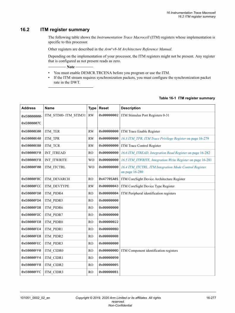
16.2 ITM register summaryThe following table shows the Instrumentation Trace Macrocell (ITM) registers whose implementation isspecific to this processor.
Other registers are described in the Arm®v8-M Architecture Reference Manual.
Depending on the implementation of your processor, the ITM registers might not be present. Any registerthat is configured as not present reads as zero.
Note
• You must enable DEMCR.TRCENA before you program or use the ITM.• If the ITM stream requires synchronization packets, you must configure the synchronization packet
rate in the DWT.
Table 16-1 ITM register summary
Address Name Type Reset Description
0xE0000000-
0xE000007C
ITM_STIM0- ITM_STIM31 RW 0x00000002 ITM Stimulus Port Registers 0-31
0xE0000E00 ITM_TER RW 0x00000000 ITM Trace Enable Register
0xE0000E40 ITM_TPR RW 0x00000000 16.3 ITM_TPR, ITM Trace Privilege Register on page 16-279
0xE0000E80 ITM_TCR RW 0x00000000 ITM Trace Control Register
0xE0000EF0 INT_ITREAD RO 0x00000000 16.6 ITM_ITREAD, Integration Read Register on page 16-282
0xE0000EF8 INT_ITWRITE WO 0x00000000 16.5 ITM_ITWRITE, Integration Write Register on page 16-281
0xE0000F00 ITM_ITCTRL WO 0x00000000 16.4 ITM_ITCTRL, ITM Integration Mode Control Registeron page 16-280
0xE0000FBC ITM_DEVARCH RO 0x47701A01 ITM CoreSight Device Architecture Register
0xE0000FCC ITM_DEVTYPE RW 0x00000043 ITM CoreSight Device Type Register
0xE0000FD0 ITM_PIDR4 RO 0x00000004 ITM Peripheral identification registers
0xE0000FD4 ITM_PIDR5 RO 0x00000000
0xE0000FD8 ITM_PIDR6 RO 0x00000000
0xE0000FDC ITM_PIDR7 RO 0x00000000
0xE0000FE0 ITM_PIDR0 RO 0x00000022
0xE0000FE4 ITM_PIDR1 RO 0x000000BD
0xE0000FE8 ITM_PIDR2 RO 0x0000000B
0xE0000FEC ITM_PIDR3 RO 0x00000000
0xE0000FF0 ITM_CIDR0 RO 0x0000000D ITM Component identification registers
0xE0000FF4 ITM_CIDR1 RO 0x00000090
0xE0000FF8 ITM_CIDR2 RO 0x00000005
0xE0000FFC ITM_CIDR3 RO 0x000000B1
16 Instrumentation Trace Macrocell16.2 ITM register summary
101051_0002_02_en Copyright © 2019, 2020 Arm Limited or its affiliates. All rightsreserved.
16-277
Non-Confidential

Note
ITM registers are fully accessible in privileged mode.
In user mode:• All registers can be read.• Only the Stimulus registers and Trace Enable registers can be written, and only when the
corresponding Trace Privilege Register bit is set.• Writes to registers other than the Stimulus registers and Trace Enable registers are invalid and they
are ignored.
When the Security Extension is included in the Cortex-M55 processor and if Secure non-invasive debugauthentication is not enabled, writes to the Stimulus registers from the software running in Secure stateare ignored.
16 Instrumentation Trace Macrocell16.2 ITM register summary
101051_0002_02_en Copyright © 2019, 2020 Arm Limited or its affiliates. All rightsreserved.
16-278
Non-Confidential
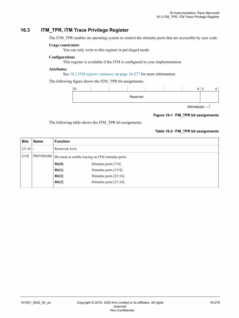
16.3 ITM_TPR, ITM Trace Privilege RegisterThe ITM_TPR enables an operating system to control the stimulus ports that are accessible by user code.
Usage constraintsYou can only write to this register in privileged mode.
ConfigurationsThis register is available if the ITM is configured in your implementation.
AttributesSee 16.2 ITM register summary on page 16-277 for more information.
The following figure shows the ITM_TPR bit assignments.
Reserved
31 4 3 0
PRIVMASK
Figure 16-1 ITM_TPR bit assignments
The following table shows the ITM_TPR bit assignments.
Table 16-2 ITM_TPR bit assignments
Bits Name Function
[31:4] - Reserved, RES0.
[3:0] PRIVMASK Bit mask to enable tracing on ITM stimulus ports:
Bit[0] Stimulus ports [7:0].
Bit[1] Stimulus ports [15:8].
Bit[2] Stimulus ports [23:16].
Bit[3] Stimulus ports [31:24].
16 Instrumentation Trace Macrocell16.3 ITM_TPR, ITM Trace Privilege Register
101051_0002_02_en Copyright © 2019, 2020 Arm Limited or its affiliates. All rightsreserved.
16-279
Non-Confidential
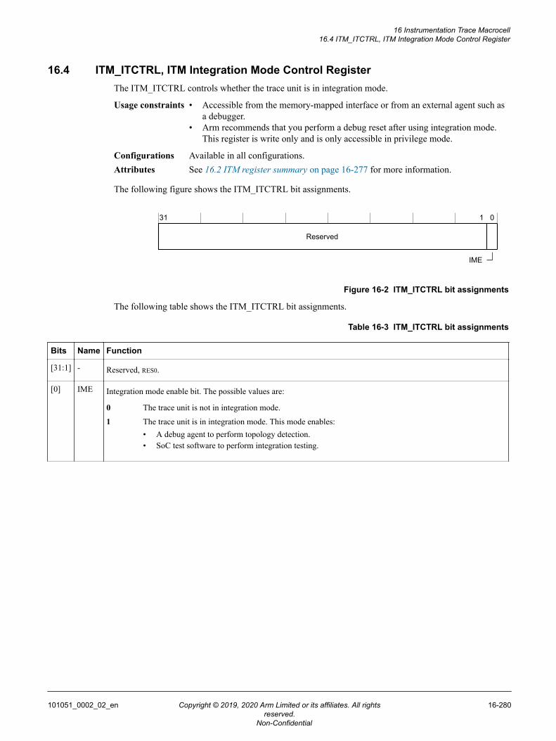
16.4 ITM_ITCTRL, ITM Integration Mode Control RegisterThe ITM_ITCTRL controls whether the trace unit is in integration mode.
Usage constraints • Accessible from the memory-mapped interface or from an external agent such asa debugger.
• Arm recommends that you perform a debug reset after using integration mode.This register is write only and is only accessible in privilege mode.
Configurations Available in all configurations.Attributes See 16.2 ITM register summary on page 16-277 for more information.
The following figure shows the ITM_ITCTRL bit assignments.
31 0
IME
1
Reserved
Figure 16-2 ITM_ITCTRL bit assignments
The following table shows the ITM_ITCTRL bit assignments.
Table 16-3 ITM_ITCTRL bit assignments
Bits Name Function
[31:1] - Reserved, RES0.
[0] IME Integration mode enable bit. The possible values are:
0 The trace unit is not in integration mode.
1 The trace unit is in integration mode. This mode enables:• A debug agent to perform topology detection.• SoC test software to perform integration testing.
16 Instrumentation Trace Macrocell16.4 ITM_ITCTRL, ITM Integration Mode Control Register
101051_0002_02_en Copyright © 2019, 2020 Arm Limited or its affiliates. All rightsreserved.
16-280
Non-Confidential
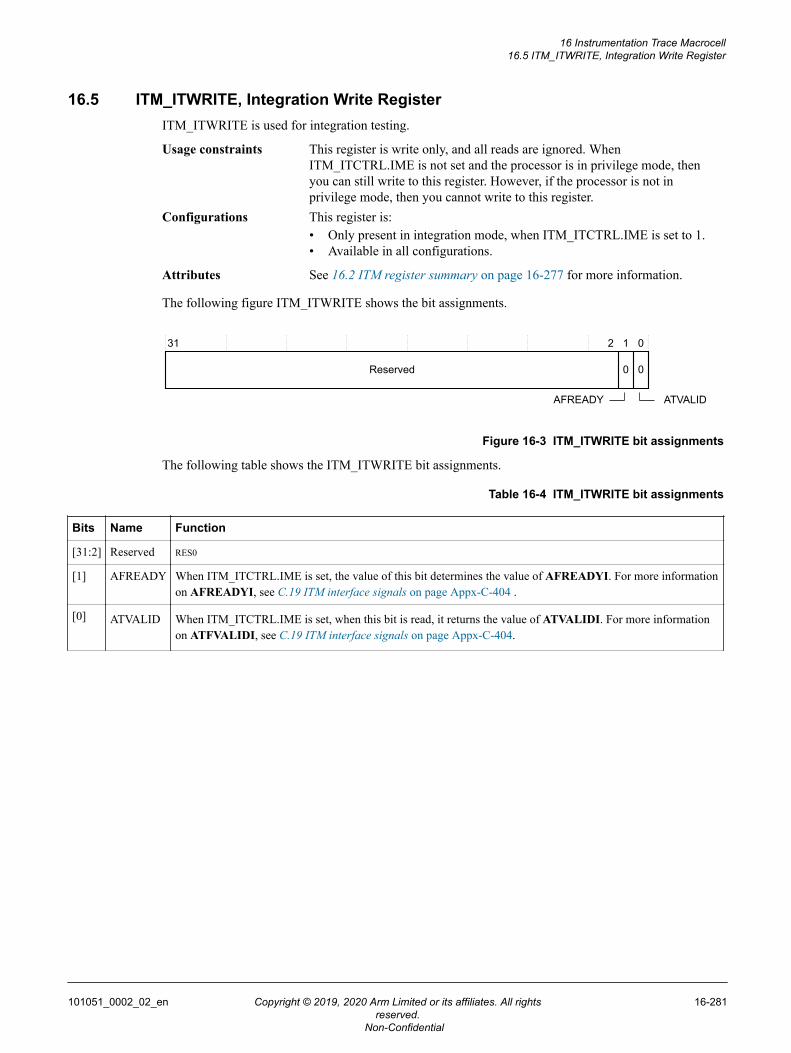
16.5 ITM_ITWRITE, Integration Write RegisterITM_ITWRITE is used for integration testing.
Usage constraints This register is write only, and all reads are ignored. WhenITM_ITCTRL.IME is not set and the processor is in privilege mode, thenyou can still write to this register. However, if the processor is not inprivilege mode, then you cannot write to this register.
Configurations This register is:• Only present in integration mode, when ITM_ITCTRL.IME is set to 1.• Available in all configurations.
Attributes See 16.2 ITM register summary on page 16-277 for more information.
The following figure ITM_ITWRITE shows the bit assignments.
0
31 2 1 0
0Reserved
AFREADY ATVALID
Figure 16-3 ITM_ITWRITE bit assignments
The following table shows the ITM_ITWRITE bit assignments.
Table 16-4 ITM_ITWRITE bit assignments
Bits Name Function
[31:2] Reserved RES0
[1] AFREADY When ITM_ITCTRL.IME is set, the value of this bit determines the value of AFREADYI. For more informationon AFREADYI, see C.19 ITM interface signals on page Appx-C-404 .
[0] ATVALID When ITM_ITCTRL.IME is set, when this bit is read, it returns the value of ATVALIDI. For more informationon ATFVALIDI, see C.19 ITM interface signals on page Appx-C-404.
16 Instrumentation Trace Macrocell16.5 ITM_ITWRITE, Integration Write Register
101051_0002_02_en Copyright © 2019, 2020 Arm Limited or its affiliates. All rightsreserved.
16-281
Non-Confidential
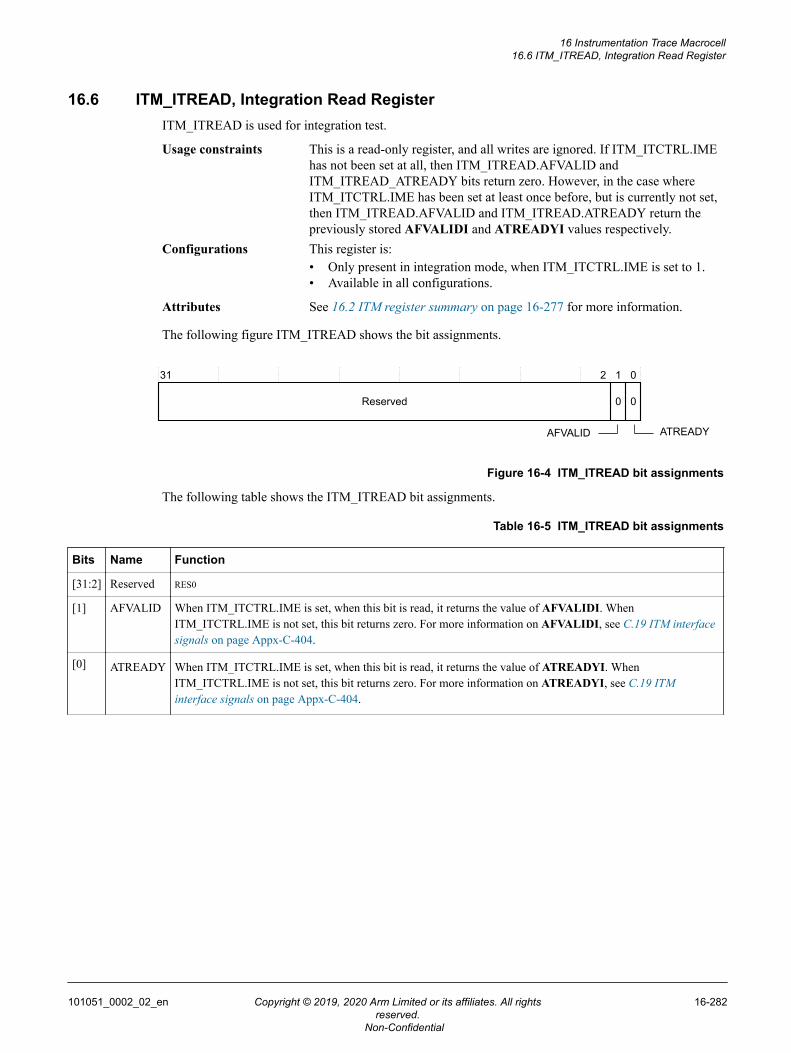
16.6 ITM_ITREAD, Integration Read RegisterITM_ITREAD is used for integration test.
Usage constraints This is a read-only register, and all writes are ignored. If ITM_ITCTRL.IMEhas not been set at all, then ITM_ITREAD.AFVALID andITM_ITREAD_ATREADY bits return zero. However, in the case whereITM_ITCTRL.IME has been set at least once before, but is currently not set,then ITM_ITREAD.AFVALID and ITM_ITREAD.ATREADY return thepreviously stored AFVALIDI and ATREADYI values respectively.
Configurations This register is:• Only present in integration mode, when ITM_ITCTRL.IME is set to 1.• Available in all configurations.
Attributes See 16.2 ITM register summary on page 16-277 for more information.
The following figure ITM_ITREAD shows the bit assignments.
0
31 2 1 0
0Reserved
AFVALID ATREADY
Figure 16-4 ITM_ITREAD bit assignments
The following table shows the ITM_ITREAD bit assignments.
Table 16-5 ITM_ITREAD bit assignments
Bits Name Function
[31:2] Reserved RES0
[1] AFVALID When ITM_ITCTRL.IME is set, when this bit is read, it returns the value of AFVALIDI. WhenITM_ITCTRL.IME is not set, this bit returns zero. For more information on AFVALIDI, see C.19 ITM interfacesignals on page Appx-C-404.
[0] ATREADY When ITM_ITCTRL.IME is set, when this bit is read, it returns the value of ATREADYI. WhenITM_ITCTRL.IME is not set, this bit returns zero. For more information on ATREADYI, see C.19 ITMinterface signals on page Appx-C-404.
16 Instrumentation Trace Macrocell16.6 ITM_ITREAD, Integration Read Register
101051_0002_02_en Copyright © 2019, 2020 Arm Limited or its affiliates. All rightsreserved.
16-282
Non-Confidential
Chapter 17Data Watchpoint and Trace
This chapter describes the Data Watchpoint and Trace (DWT).
It contains the following sections:• 17.1 DWT features on page 17-284.• 17.2 DWT debug access control on page 17-286.• 17.3 DWT comparators on page 17-288.• 17.4 Cycle counter and profiling counters on page 17-289.• 17.5 DWT register summary on page 17-290.
101051_0002_02_en Copyright © 2019, 2020 Arm Limited or its affiliates. All rightsreserved.
17-283
Non-Confidential
17.1 DWT featuresThe Cortex-M55 processor Data Watchpoint and Trace (DWT) unit has the following features:
• Watchpoints• Data tracing• Trace control signaling based on comparator match which can be used to control the optional
Embedded Trace Macrocell (ETM) and Cross Trigger Interface (CTI) if they are configured in theprocessor
• Program Counter (PC) tracing• Cycle count matching• Additional PC sampling:
— PC sample trace output as a result of a cycle count event— External PC sampling using a PC sample register
• Exception tracing• Match event tracing• Performance profiling counters• An implementation of the Performance Monitoring Unit (PMU), sharing the event counters with the
regular Cortex‑M profiling counters. PMU events can be traced through the Instrumentation TraceMacrocell (ITM) and can be used to raise interrupts
• Support for the Digital Signal Processing (DSP) extension
The DWT receives data transactions and instruction execution information from the processor core.Exception information and core profiling information is also delivered to the DWT from the processorcore. The DWT comparators can be configured for two simultaneous data value comparisons.
The DWT compares instruction and data information using the comparators that are programmedaccording to the debug architecture. The results of these comparisons and any profiling counter andexception information are passed to the packet generator so it can generate, buffer, and arbitrate packetsto be sent to the ITM.
Additional functionality includes ETM triggers using the CMPMATCH signals and invasive watchpointdebugging.
According to the architecture, all DWT debug events are asynchronous and are not recognized on theinstruction which caused the event. Therefore the DWT PC-matching functionality cannot be used toimplement breakpoints in the processor.
The Cortex-M55 processor DWT supports tracing of exceptions using an interface to the processor. Theexception state information is determined from the processor core exception control signals whichindicate the following events:
• Idle.• Exception entry.• Exception exit.• Exception return.
When exception trace is enabled in DWT_CTRL.EXCTRCENA, these events cause the DWT to outputexception packets to the ITM.
Important
Data Trace Data Address packets are generated when there is a data address range match and if thecomparator pair has been programmed accordingly. For more information on Data Trace Data Addresspackets, see the Arm®v8-M Architecture Reference Manual.
When there is a data address range match where the address of the first access is below the lower limit ofthe programmed address range, the Data Trace Data Address packet that is generated contains the
17 Data Watchpoint and Trace17.1 DWT features
101051_0002_02_en Copyright © 2019, 2020 Arm Limited or its affiliates. All rightsreserved.
17-284
Non-Confidential
address of the first access instead of the address of the first matching access. In this case, however,debugger tools can reconstruct the address of the first matching access by considering the following:• A Data Trace Data Address packet has been generated, implying that there is a data address range
match.• The data address that is stored in the Data Trace Data Address packet is lower than the programmed
lower range limit.
Therefore, the debugger tool can reconstruct the address of the first matching access to be equal to theprogrammed lower limit value of the address range.
17 Data Watchpoint and Trace17.1 DWT features
101051_0002_02_en Copyright © 2019, 2020 Arm Limited or its affiliates. All rightsreserved.
17-285
Non-Confidential
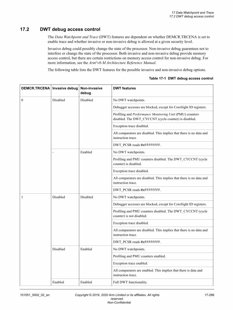
17.2 DWT debug access controlThe Data Watchpoint and Trace (DWT) features are dependent on whether DEMCR.TRCENA is set toenable trace and whether invasive or non-invasive debug is allowed at a given security level.
Invasive debug could possibly change the state of the processor. Non-invasive debug guarantees not tointerfere or change the state of the processor. Both invasive and non-invasive debug provide memoryaccess control, but there are certain restrictions on memory access control for non-invasive debug. Formore information, see the Arm®v8-M Architecture Reference Manual.
The following table lists the DWT features for the possible invasive and non-invasive debug options.
Table 17-1 DWT debug access control
DEMCR.TRCENA Invasive debug Non-invasivedebug
DWT features
0 Disabled Disabled No DWT watchpoints.
Debugger accesses are blocked, except for CoreSight ID registers.
Profiling and Performance Monitoring Unit (PMU) countersdisabled. The DWT_CYCCNT (cycle counter) is disabled.
Exception trace disabled.
All comparators are disabled. This implies that there is no data andinstruction trace.
DWT_PCSR reads 0xFFFFFFFF.
- Enabled No DWT watchpoints.
Profiling and PMU counters disabled. The DWT_CYCCNT (cyclecounter) is disabled.
Exception trace disabled.
All comparators are disabled. This implies that there is no data andinstruction trace.
DWT_PCSR reads 0xFFFFFFFF.
1 Disabled Disabled No DWT watchpoints.
Debugger accesses are blocked, except for CoreSight ID registers.
Profiling and PMU counters disabled. The DWT_CYCCNT (cyclecounter) is not disabled.
Exception trace disabled.
All comparators are disabled. This implies that there is no data andinstruction trace.
DWT_PCSR reads 0xFFFFFFFF.
Disabled Enabled No DWT watchpoints.
Profiling and PMU counters enabled.
Exception trace enabled.
All comparators are enabled. This implies that there is data andinstruction trace.
Enabled Enabled Full DWT functionality.
17 Data Watchpoint and Trace17.2 DWT debug access control
101051_0002_02_en Copyright © 2019, 2020 Arm Limited or its affiliates. All rightsreserved.
17-286
Non-Confidential

Note
For a description of DEMCR and DWT_PCSR, see the Arm®v8-M Architecture Reference Manual.
17 Data Watchpoint and Trace17.2 DWT debug access control
101051_0002_02_en Copyright © 2019, 2020 Arm Limited or its affiliates. All rightsreserved.
17-287
Non-Confidential
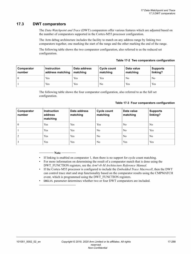
17.3 DWT comparatorsThe Data Watchpoint and Trace (DWT) comparators offer various features which are adjusted based onthe number of comparators supported in the Cortex-M55 processor configuration.
The Arm debug architecture includes the facility to match on any address range by linking twocomparators together, one marking the start of the range and the other marking the end of the range.
The following table shows the two comparator configuration, also referred to as the reduced setconfiguration.
Table 17-2 Two comparators configuration
Comparatornumber
Instructionaddress matching
Data addressmatching
Cycle countmatching
Data valuematching
Supportslinking?
0 Yes Yes Yes No No
1 Yes Yes No Yes Yes
The following table shows the four comparator configuration, also referred to as the full setconfiguration.
Table 17-3 Four comparators configuration
Comparatornumber
Instructionaddressmatching
Data addressmatching
Cycle countmatching
Data valuematching
Supportslinking?
0 Yes Yes Yes No No
1 Yes Yes No No Yes
2 Yes Yes No No No
3 Yes Yes No Yes Yes
Note
• If linking is enabled on comparator 1, then there is no support for cycle count matching.• For more information on determining the result of a comparator match that is done using the
DWT_FUNCTION registers, see the Arm®v8-M Architecture Reference Manual.• If the Cortex-M55 processor is configured to include the Embedded Trace Macrocell, then the DWT
can control trace start and stop functionality based on the comparator results using the CMPMATCHevent, which is programmed using the DWT_FUNCTION registers.
• DBGLVL parameter determines whether two or four DWT comparators are included.
17 Data Watchpoint and Trace17.3 DWT comparators
101051_0002_02_en Copyright © 2019, 2020 Arm Limited or its affiliates. All rightsreserved.
17-288
Non-Confidential
17.4 Cycle counter and profiling countersThe Cortex-M55 DWT supports a cycle counter and profiling counters.
Cycle counter
When enabled in DWT_CTRL, the 32-bit cycle counter, DWT_CYCCNT, increments each cycle unlessthe processor is in debug halt state. When the cycle counter is disabled, all functionality associated withthe cycle counter is also disabled.
If the processor includes support for the Security Extension then the DWT_CTRL.CYCDISS bit fielddisables the cycle counter increment when the processor is executing secure code. This can be useful forgenerating CPI measurements for Non-secure applications.
Profiling counters
The profiling counters can be configured to generate events on overflow using DWT_CTRL fields.
CPI Counter (DWT_CPICNT)
The 8-bit CPI counter is incremented for every additional cycle, that is, greater than one taken toexecute a non-load or store instruction. This counter must also be incremented for every cyclewhere fetch is stalled.
Exception Overhead Counter (DWT_EXCCNT)
The 8-bit Exception Overhead Counter is incremented for every cycle associated with exceptionentry and return. This includes stacking, unstacking, and preemption and tail-chaining, in caseswhere additional registers must be stacked due to a change in Security state between exceptions.Register stacking associated with floating-point lazy context saving is also included in thiscounter.
Sleep Overhead Counter (DWT_SLEEPCNT)
The 8-bit Sleep Overhead Counter is incremented for every cycle associated for power saving.For example, WFI and WFE exceptions.
Load-Store Counter (DWT_LSUCNT)
The 8-bit Load-Store Counter is incremented for every additional cycle that is greater than onetaken to execute a load-store instruction.
Fold Counter (DWT_FOLDCNT)
The 8-bit Fold Counter counts folded instructions and increments for every instruction executedin zero cycles. All folded instructions are dual-issued. For example, for a dual-issued pair ofinstructions, the counter increments by one to reflect this.
17 Data Watchpoint and Trace17.4 Cycle counter and profiling counters
101051_0002_02_en Copyright © 2019, 2020 Arm Limited or its affiliates. All rightsreserved.
17-289
Non-Confidential
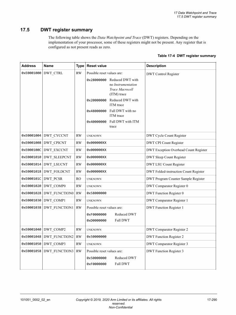
17.5 DWT register summaryThe following table shows the Data Watchpoint and Trace (DWT) registers. Depending on theimplementation of your processor, some of these registers might not be present. Any register that isconfigured as not present reads as zero.
Table 17-4 DWT register summary
Address Name Type Reset value Description
0xE0001000 DWT_CTRL RW Possible reset values are:
0x28000000 Reduced DWT withno InstrumentationTrace Macrocell(ITM) trace
0x20000000 Reduced DWT withITM trace
0x48000000 Full DWT with noITM trace
0x40000000 Full DWT with ITMtrace
DWT Control Register
0xE0001004 DWT_CYCCNT RW UNKNOWN DWT Cycle Count Register
0xE0001008 DWT_CPICNT RW 0x000000XX DWT CPI Count Register
0xE000100C DWT_EXCCNT RW 0x000000XX DWT Exception Overhead Count Register
0xE0001010 DWT_SLEEPCNT RW 0x000000XX DWT Sleep Count Register
0xE0001014 DWT_LSUCNT RW 0x000000XX DWT LSU Count Register
0xE0001018 DWT_FOLDCNT RW 0x000000XX DWT Folded-instruction Count Register
0xE000101C DWT_PCSR RO UNKNOWN DWT Program Counter Sample Register
0xE0001020 DWT_COMP0 RW UNKNOWN DWT Comparator Register 0
0xE0001028 DWT_FUNCTION0 RW 0x58000000 DWT Function Register 0
0xE0001030 DWT_COMP1 RW UNKNOWN DWT Comparator Register 1
0xE0001038 DWT_FUNCTION1 RW Possible reset values are:
0xF0000000 Reduced DWT
0xD0000000 Full DWT
DWT Function Register 1
0xE0001040 DWT_COMP2 RW UNKNOWN DWT Comparator Register 2
0xE0001048 DWT_FUNCTION2 RW 0x50000000 DWT Function Register 2
0xE0001050 DWT_COMP3 RW UNKNOWN DWT Comparator Register 3
0xE0001058 DWT_FUNCTION3 RW Possible reset values are:
0x50000000 Reduced DWT
0xF0000000 Full DWT
DWT Function Register 3
17 Data Watchpoint and Trace17.5 DWT register summary
101051_0002_02_en Copyright © 2019, 2020 Arm Limited or its affiliates. All rightsreserved.
17-290
Non-Confidential
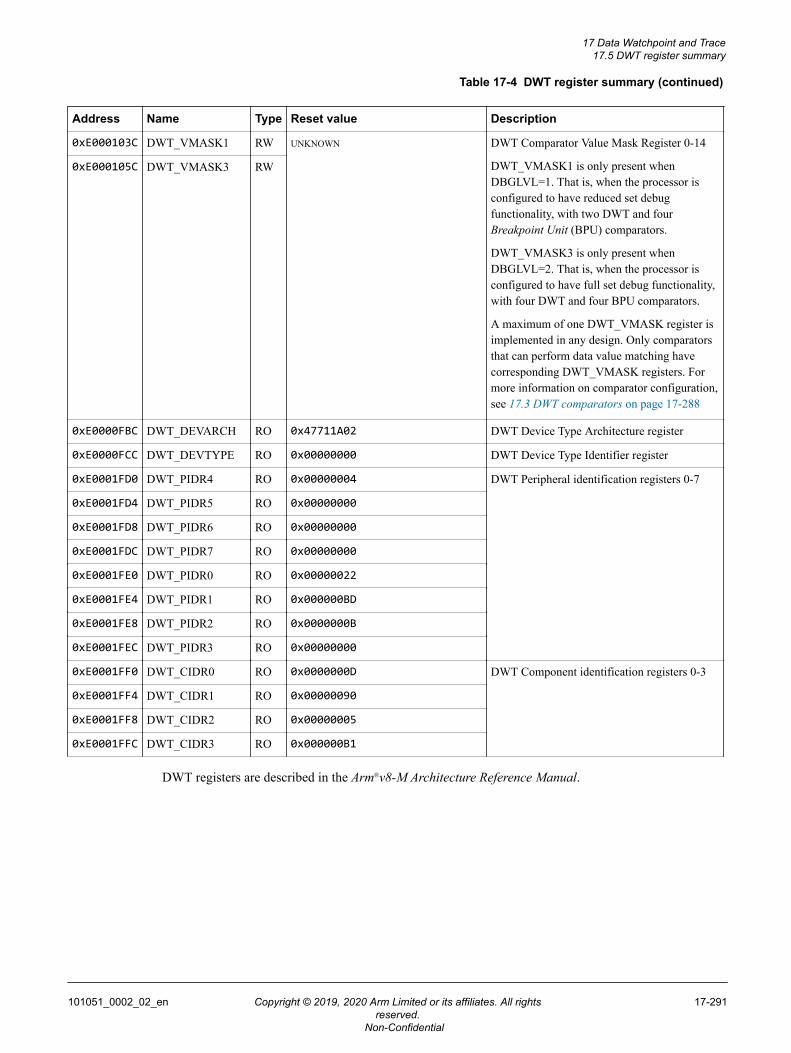
Table 17-4 DWT register summary (continued)
Address Name Type Reset value Description
0xE000103C DWT_VMASK1 RW UNKNOWN DWT Comparator Value Mask Register 0-14
DWT_VMASK1 is only present whenDBGLVL=1. That is, when the processor isconfigured to have reduced set debugfunctionality, with two DWT and fourBreakpoint Unit (BPU) comparators.
DWT_VMASK3 is only present whenDBGLVL=2. That is, when the processor isconfigured to have full set debug functionality,with four DWT and four BPU comparators.
A maximum of one DWT_VMASK register isimplemented in any design. Only comparatorsthat can perform data value matching havecorresponding DWT_VMASK registers. Formore information on comparator configuration,see 17.3 DWT comparators on page 17-288
0xE000105C DWT_VMASK3 RW
0xE0000FBC DWT_DEVARCH RO 0x47711A02 DWT Device Type Architecture register
0xE0000FCC DWT_DEVTYPE RO 0x00000000 DWT Device Type Identifier register
0xE0001FD0 DWT_PIDR4 RO 0x00000004 DWT Peripheral identification registers 0-7
0xE0001FD4 DWT_PIDR5 RO 0x00000000
0xE0001FD8 DWT_PIDR6 RO 0x00000000
0xE0001FDC DWT_PIDR7 RO 0x00000000
0xE0001FE0 DWT_PIDR0 RO 0x00000022
0xE0001FE4 DWT_PIDR1 RO 0x000000BD
0xE0001FE8 DWT_PIDR2 RO 0x0000000B
0xE0001FEC DWT_PIDR3 RO 0x00000000
0xE0001FF0 DWT_CIDR0 RO 0x0000000D DWT Component identification registers 0-3
0xE0001FF4 DWT_CIDR1 RO 0x00000090
0xE0001FF8 DWT_CIDR2 RO 0x00000005
0xE0001FFC DWT_CIDR3 RO 0x000000B1
DWT registers are described in the Arm®v8-M Architecture Reference Manual.
17 Data Watchpoint and Trace17.5 DWT register summary
101051_0002_02_en Copyright © 2019, 2020 Arm Limited or its affiliates. All rightsreserved.
17-291
Non-Confidential
Chapter 18Cross Trigger Interface
This chapter describes the Cross Trigger Interface (CTI).
It contains the following sections:• 18.1 CTI features on page 18-294.• 18.2 CTI register summary on page 18-296.• 18.3 CTI_CONTROL, CTI Control Register on page 18-298.• 18.4 CTI_INACK, CTI Interrupt Acknowledge Register on page 18-299.• 18.5 CTI_APPSET, CTI Application Channel Set Register on page 18-300.• 18.6 CTI_APPCLR, CTI Application Channel Clear Register on page 18-301.• 18.7 CTI_APPPULSE, CTI Application Channel Pulse Register on page 18-302.• 18.8 CTI_INEN<n>, n=0-5, CTI Trigger <n> to Channel Enable Register on page 18-303.• 18.9 CTI_OUTEN<n>, n=0-7, CTI Channel <n> to Trigger Enable Register on page 18-304.• 18.10 CTI_TRIGINSTATUS, CTI Trigger Input Status Register on page 18-306.• 18.11 CTI_TRIGOUTSTATUS, CTI Trigger Output Status Register on page 18-307.• 18.12 CTI_CHINSTATUS, CTI Channel Input Status Register on page 18-308.• 18.13 CTI_CHOUTSTATUS, CTI Channel Output Status Register on page 18-309.• 18.14 CTI_CHANNELGATE, CTI Channel Gate Register on page 18-310.• 18.15 CTI_ITCHOUT, Integration Test Channel Output Register on page 18-311.• 18.16 CTI_ITTRIGOUT, Integration Test Trigger Output Register on page 18-312.• 18.17 CTI_ITCHIN, Integration Test Channel Input Register on page 18-314.• 18.18 CTI_ITTRIGIN, Integration Test Trigger Input Register on page 18-315.• 18.19 CTI_ITCONTROL, Integration Mode Control Register on page 18-316.• 18.20 CTI_DEVARCH, Device Architecture Register on page 18-317.• 18.21 CTI_DEVID, Device Configuration Register on page 18-318.• 18.22 CTI_DEVTYPE, Device Type Identifier Register on page 18-319.• 18.23 CTI_PIDR4, Peripheral Identification Register 4 on page 18-320.
101051_0002_02_en Copyright © 2019, 2020 Arm Limited or its affiliates. All rightsreserved.
18-292
Non-Confidential
• 18.24 CTI_PIDR5, Peripheral Identification Register 5 on page 18-321.• 18.25 CTI_PIDR6, Peripheral Identification Register 6 on page 18-322.• 18.26 CTI_PIDR7, Peripheral Identification Register 7 on page 18-323.• 18.27 CTI_PIDR0, Peripheral Identification Register 0 on page 18-324.• 18.28 CTI_PIDR1, Peripheral Identification Register 1 on page 18-325.• 18.29 CTI_PIDR2, Peripheral Identification Register 2 on page 18-326.• 18.30 CTI_PIDR3, Peripheral Identification Register 3 on page 18-327.• 18.31 CTI_ CIDR0, Component Identification Register 0 on page 18-328.• 18.32 CTI_ CIDR1, Component Identification Register 1 on page 18-329.• 18.33 CTI_ CIDR2, Component Identification Register 2 on page 18-330.• 18.34 CTI_ CIDR3, Component Identification Register 3 on page 18-331.
18 Cross Trigger Interface
101051_0002_02_en Copyright © 2019, 2020 Arm Limited or its affiliates. All rightsreserved.
18-293
Non-Confidential
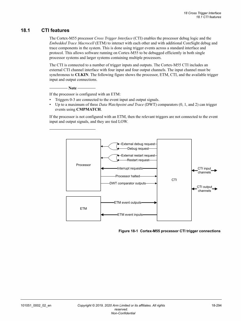
18.1 CTI featuresThe Cortex-M55 processor Cross Trigger Interface (CTI) enables the processor debug logic and theEmbedded Trace Macrocell (ETM) to interact with each other and with additional CoreSight debug andtrace components in the system. This is done using trigger events across a standard interface andprotocol. This allows software running on Cortex-M55 to be debugged efficiently in both singleprocessor systems and larger systems containing multiple processors.
The CTI is connected to a number of trigger inputs and outputs. The Cortex-M55 CTI includes anexternal CTI channel interface with four input and four output channels. The input channel must besynchronous to CLKIN. The following figure shows the processor, ETM, CTI, and the available triggerinput and output connections.
Note
If the processor is configured with an ETM:• Triggers 0-3 are connected to the event input and output signals.• Up to a maximum of three Data Watchpoint and Trace (DWT) comparators (0, 1, and 2) can trigger
events using CMPMATCH.
If the processor is not configured with an ETM, then the relevant triggers are not connected to the eventinput and output signals, and they are tied LOW.
Processor
ETM
CTI
External debug requestDebug request
External restart requestRestart request
Interrupt requests
Processor halted
DWT comparator outputs
ETM event outputs
ETM event inputs
CTI input channels
CTI output channels
Figure 18-1 Cortex-M55 processor CTI trigger connections
18 Cross Trigger Interface18.1 CTI features
101051_0002_02_en Copyright © 2019, 2020 Arm Limited or its affiliates. All rightsreserved.
18-294
Non-Confidential
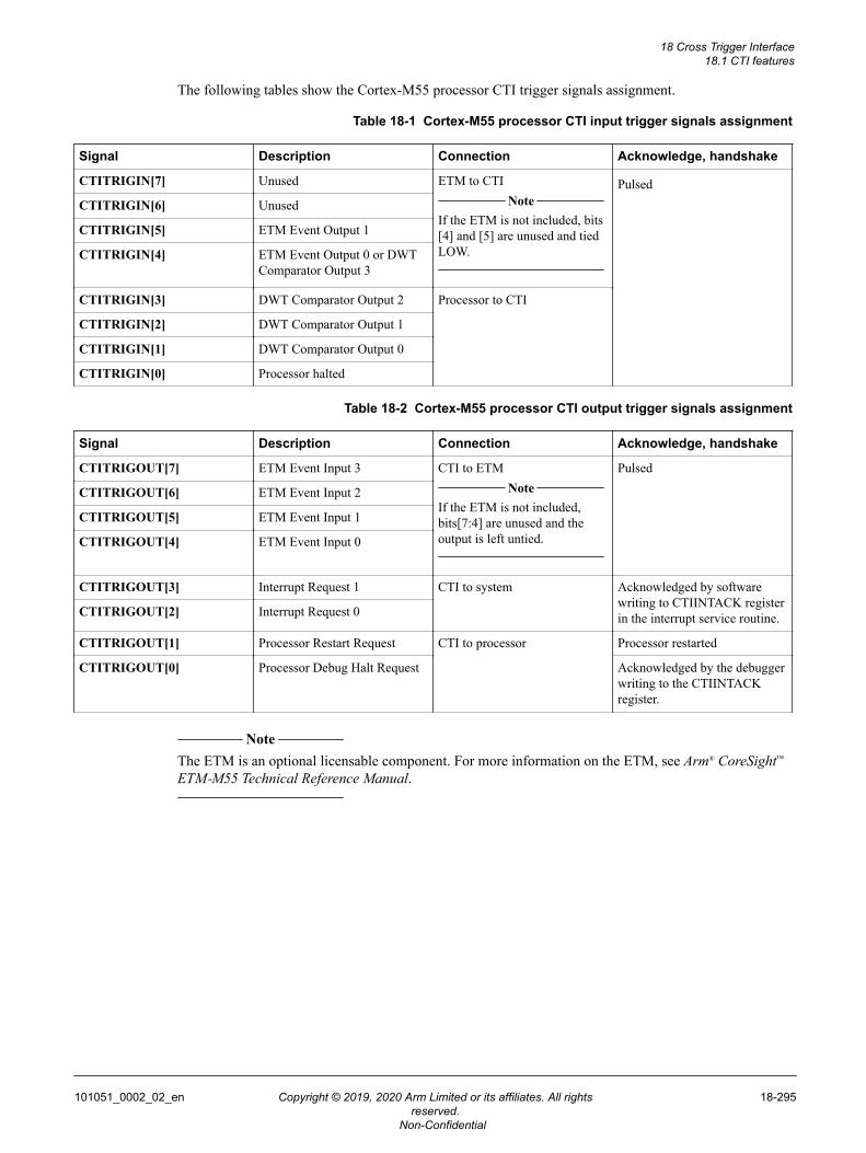
The following tables show the Cortex-M55 processor CTI trigger signals assignment.
Table 18-1 Cortex-M55 processor CTI input trigger signals assignment
Signal Description Connection Acknowledge, handshake
CTITRIGIN[7] Unused ETM to CTI Note
If the ETM is not included, bits[4] and [5] are unused and tiedLOW.
PulsedCTITRIGIN[6] Unused
CTITRIGIN[5] ETM Event Output 1
CTITRIGIN[4] ETM Event Output 0 or DWTComparator Output 3
CTITRIGIN[3] DWT Comparator Output 2 Processor to CTI
CTITRIGIN[2] DWT Comparator Output 1
CTITRIGIN[1] DWT Comparator Output 0
CTITRIGIN[0] Processor halted
Table 18-2 Cortex-M55 processor CTI output trigger signals assignment
Signal Description Connection Acknowledge, handshake
CTITRIGOUT[7] ETM Event Input 3 CTI to ETM Note
If the ETM is not included,bits[7:4] are unused and theoutput is left untied.
Pulsed
CTITRIGOUT[6] ETM Event Input 2
CTITRIGOUT[5] ETM Event Input 1
CTITRIGOUT[4] ETM Event Input 0
CTITRIGOUT[3] Interrupt Request 1 CTI to system Acknowledged by softwarewriting to CTIINTACK registerin the interrupt service routine.CTITRIGOUT[2] Interrupt Request 0
CTITRIGOUT[1] Processor Restart Request CTI to processor Processor restarted
CTITRIGOUT[0] Processor Debug Halt Request Acknowledged by the debuggerwriting to the CTIINTACKregister.
Note
The ETM is an optional licensable component. For more information on the ETM, see Arm® CoreSight™
ETM‑M55 Technical Reference Manual.
18 Cross Trigger Interface18.1 CTI features
101051_0002_02_en Copyright © 2019, 2020 Arm Limited or its affiliates. All rightsreserved.
18-295
Non-Confidential
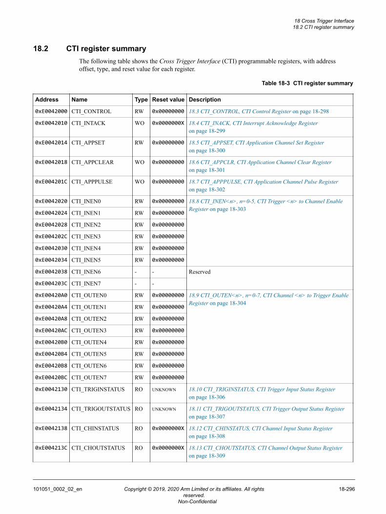
18.2 CTI register summaryThe following table shows the Cross Trigger Interface (CTI) programmable registers, with addressoffset, type, and reset value for each register.
Table 18-3 CTI register summary
Address Name Type Reset value Description
0xE0042000 CTI_CONTROL RW 0x00000000 18.3 CTI_CONTROL, CTI Control Register on page 18-298
0xE0042010 CTI_INTACK WO 0x0000000X 18.4 CTI_INACK, CTI Interrupt Acknowledge Registeron page 18-299
0xE0042014 CTI_APPSET RW 0x00000000 18.5 CTI_APPSET, CTI Application Channel Set Registeron page 18-300
0xE0042018 CTI_APPCLEAR WO 0x00000000 18.6 CTI_APPCLR, CTI Application Channel Clear Registeron page 18-301
0xE004201C CTI_APPPULSE WO 0x00000000 18.7 CTI_APPPULSE, CTI Application Channel Pulse Registeron page 18-302
0xE0042020 CTI_INEN0 RW 0x00000000 18.8 CTI_INEN<n>, n=0-5, CTI Trigger <n> to Channel EnableRegister on page 18-303
0xE0042024 CTI_INEN1 RW 0x00000000
0xE0042028 CTI_INEN2 RW 0x00000000
0xE004202C CTI_INEN3 RW 0x00000000
0xE0042030 CTI_INEN4 RW 0x00000000
0xE0042034 CTI_INEN5 RW 0x00000000
0xE0042038 CTI_INEN6 - - Reserved
0xE004203C CTI_INEN7 - -
0xE00420A0 CTI_OUTEN0 RW 0x00000000 18.9 CTI_OUTEN<n>, n=0-7, CTI Channel <n> to Trigger EnableRegister on page 18-304
0xE00420A4 CTI_OUTEN1 RW 0x00000000
0xE00420A8 CTI_OUTEN2 RW 0x00000000
0xE00420AC CTI_OUTEN3 RW 0x00000000
0xE00420B0 CTI_OUTEN4 RW 0x00000000
0xE00420B4 CTI_OUTEN5 RW 0x00000000
0xE00420B8 CTI_OUTEN6 RW 0x00000000
0xE00420BC CTI_OUTEN7 RW 0x00000000
0xE0042130 CTI_TRIGINSTATUS RO UNKNOWN 18.10 CTI_TRIGINSTATUS, CTI Trigger Input Status Registeron page 18-306
0xE0042134 CTI_TRIGOUTSTATUS RO UNKNOWN 18.11 CTI_TRIGOUTSTATUS, CTI Trigger Output Status Registeron page 18-307
0xE0042138 CTI_CHINSTATUS RO 0x0000000X 18.12 CTI_CHINSTATUS, CTI Channel Input Status Registeron page 18-308
0xE004213C CTI_CHOUTSTATUS RO 0x0000000X 18.13 CTI_CHOUTSTATUS, CTI Channel Output Status Registeron page 18-309
18 Cross Trigger Interface18.2 CTI register summary
101051_0002_02_en Copyright © 2019, 2020 Arm Limited or its affiliates. All rightsreserved.
18-296
Non-Confidential
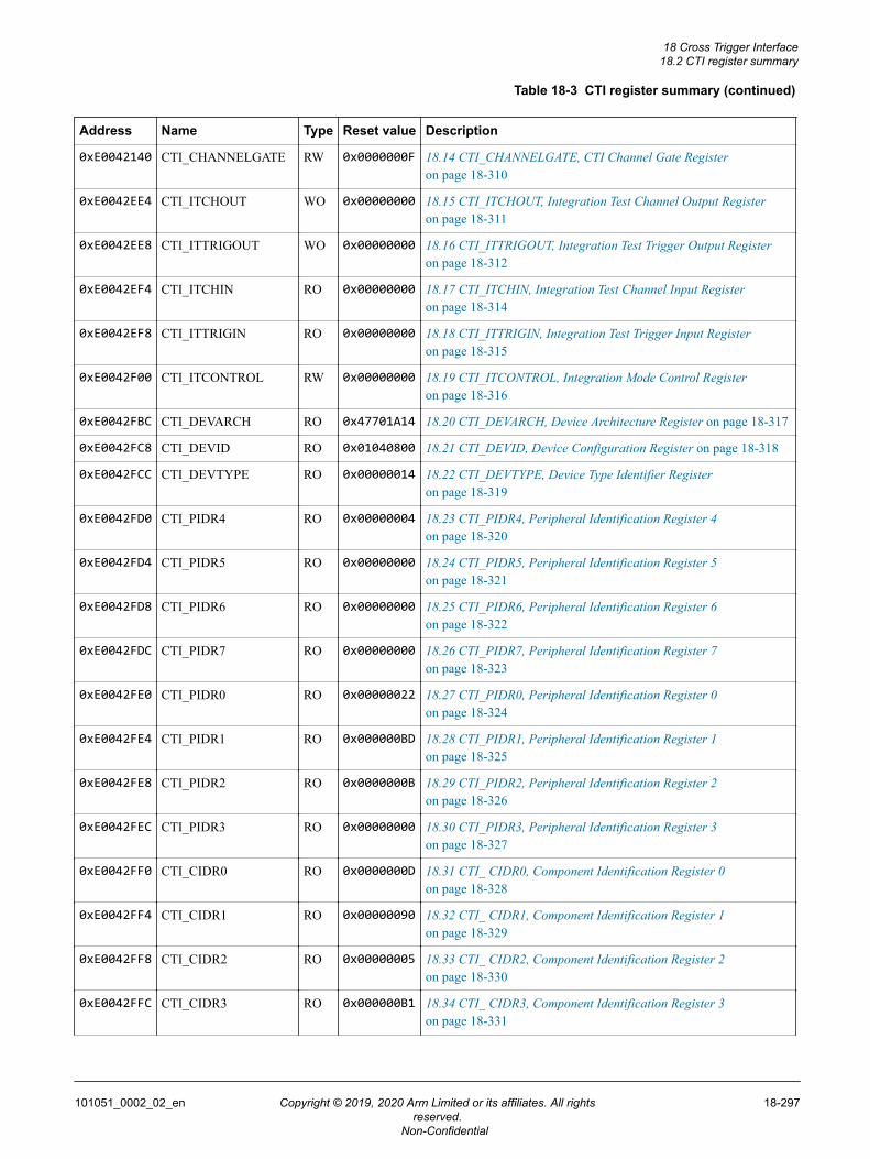
Table 18-3 CTI register summary (continued)
Address Name Type Reset value Description
0xE0042140 CTI_CHANNELGATE RW 0x0000000F 18.14 CTI_CHANNELGATE, CTI Channel Gate Registeron page 18-310
0xE0042EE4 CTI_ITCHOUT WO 0x00000000 18.15 CTI_ITCHOUT, Integration Test Channel Output Registeron page 18-311
0xE0042EE8 CTI_ITTRIGOUT WO 0x00000000 18.16 CTI_ITTRIGOUT, Integration Test Trigger Output Registeron page 18-312
0xE0042EF4 CTI_ITCHIN RO 0x00000000 18.17 CTI_ITCHIN, Integration Test Channel Input Registeron page 18-314
0xE0042EF8 CTI_ITTRIGIN RO 0x00000000 18.18 CTI_ITTRIGIN, Integration Test Trigger Input Registeron page 18-315
0xE0042F00 CTI_ITCONTROL RW 0x00000000 18.19 CTI_ITCONTROL, Integration Mode Control Registeron page 18-316
0xE0042FBC CTI_DEVARCH RO 0x47701A14 18.20 CTI_DEVARCH, Device Architecture Register on page 18-317
0xE0042FC8 CTI_DEVID RO 0x01040800 18.21 CTI_DEVID, Device Configuration Register on page 18-318
0xE0042FCC CTI_DEVTYPE RO 0x00000014 18.22 CTI_DEVTYPE, Device Type Identifier Registeron page 18-319
0xE0042FD0 CTI_PIDR4 RO 0x00000004 18.23 CTI_PIDR4, Peripheral Identification Register 4on page 18-320
0xE0042FD4 CTI_PIDR5 RO 0x00000000 18.24 CTI_PIDR5, Peripheral Identification Register 5on page 18-321
0xE0042FD8 CTI_PIDR6 RO 0x00000000 18.25 CTI_PIDR6, Peripheral Identification Register 6on page 18-322
0xE0042FDC CTI_PIDR7 RO 0x00000000 18.26 CTI_PIDR7, Peripheral Identification Register 7on page 18-323
0xE0042FE0 CTI_PIDR0 RO 0x00000022 18.27 CTI_PIDR0, Peripheral Identification Register 0on page 18-324
0xE0042FE4 CTI_PIDR1 RO 0x000000BD 18.28 CTI_PIDR1, Peripheral Identification Register 1on page 18-325
0xE0042FE8 CTI_PIDR2 RO 0x0000000B 18.29 CTI_PIDR2, Peripheral Identification Register 2on page 18-326
0xE0042FEC CTI_PIDR3 RO 0x00000000 18.30 CTI_PIDR3, Peripheral Identification Register 3on page 18-327
0xE0042FF0 CTI_CIDR0 RO 0x0000000D 18.31 CTI_ CIDR0, Component Identification Register 0on page 18-328
0xE0042FF4 CTI_CIDR1 RO 0x00000090 18.32 CTI_ CIDR1, Component Identification Register 1on page 18-329
0xE0042FF8 CTI_CIDR2 RO 0x00000005 18.33 CTI_ CIDR2, Component Identification Register 2on page 18-330
0xE0042FFC CTI_CIDR3 RO 0x000000B1 18.34 CTI_ CIDR3, Component Identification Register 3on page 18-331
18 Cross Trigger Interface18.2 CTI register summary
101051_0002_02_en Copyright © 2019, 2020 Arm Limited or its affiliates. All rightsreserved.
18-297
Non-Confidential
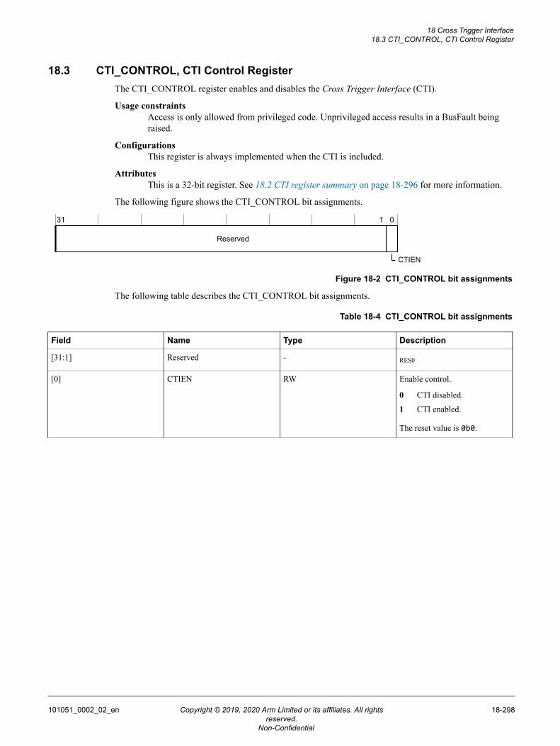
18.3 CTI_CONTROL, CTI Control RegisterThe CTI_CONTROL register enables and disables the Cross Trigger Interface (CTI).
Usage constraintsAccess is only allowed from privileged code. Unprivileged access results in a BusFault beingraised.
ConfigurationsThis register is always implemented when the CTI is included.
AttributesThis is a 32-bit register. See 18.2 CTI register summary on page 18-296 for more information.
The following figure shows the CTI_CONTROL bit assignments.
31 1 0
Reserved
CTIEN
Figure 18-2 CTI_CONTROL bit assignments
The following table describes the CTI_CONTROL bit assignments.
Table 18-4 CTI_CONTROL bit assignments
Field Name Type Description
[31:1] Reserved - RES0
[0] CTIEN RW Enable control.
0 CTI disabled.
1 CTI enabled.
The reset value is 0b0.
18 Cross Trigger Interface18.3 CTI_CONTROL, CTI Control Register
101051_0002_02_en Copyright © 2019, 2020 Arm Limited or its affiliates. All rightsreserved.
18-298
Non-Confidential
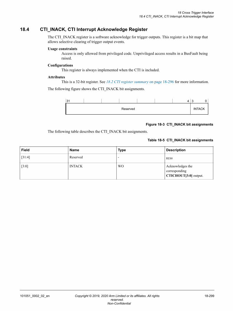
18.4 CTI_INACK, CTI Interrupt Acknowledge RegisterThe CTI_INACK register is a software acknowledge for trigger outputs. This register is a bit map thatallows selective clearing of trigger output events.
Usage constraintsAccess is only allowed from privileged code. Unprivileged access results in a BusFault beingraised.
ConfigurationsThis register is always implemented when the CTI is included.
AttributesThis is a 32-bit register. See 18.2 CTI register summary on page 18-296 for more information.
The following figure shows the CTI_INACK bit assignments.
31 0
INTACK
3
Reserved
4
Figure 18-3 CTI_INACK bit assignments
The following table describes the CTI_INACK bit assignments.
Table 18-5 CTI_INACK bit assignments
Field Name Type Description
[31:4] Reserved - RES0
[3:0] INTACK WO Acknowledges thecorrespondingCTICHOUT[3:0] output.
18 Cross Trigger Interface18.4 CTI_INACK, CTI Interrupt Acknowledge Register
101051_0002_02_en Copyright © 2019, 2020 Arm Limited or its affiliates. All rightsreserved.
18-299
Non-Confidential
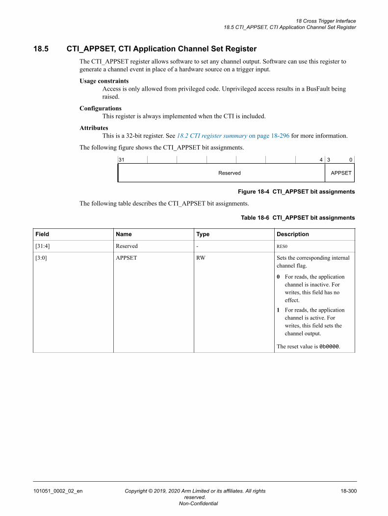
18.5 CTI_APPSET, CTI Application Channel Set RegisterThe CTI_APPSET register allows software to set any channel output. Software can use this register togenerate a channel event in place of a hardware source on a trigger input.
Usage constraintsAccess is only allowed from privileged code. Unprivileged access results in a BusFault beingraised.
ConfigurationsThis register is always implemented when the CTI is included.
AttributesThis is a 32-bit register. See 18.2 CTI register summary on page 18-296 for more information.
The following figure shows the CTI_APPSET bit assignments.
31 4 3 0
APPSETReserved
Figure 18-4 CTI_APPSET bit assignments
The following table describes the CTI_APPSET bit assignments.
Table 18-6 CTI_APPSET bit assignments
Field Name Type Description
[31:4] Reserved - RES0
[3:0] APPSET RW Sets the corresponding internalchannel flag.
0 For reads, the applicationchannel is inactive. Forwrites, this field has noeffect.
1 For reads, the applicationchannel is active. Forwrites, this field sets thechannel output.
The reset value is 0b0000.
18 Cross Trigger Interface18.5 CTI_APPSET, CTI Application Channel Set Register
101051_0002_02_en Copyright © 2019, 2020 Arm Limited or its affiliates. All rightsreserved.
18-300
Non-Confidential
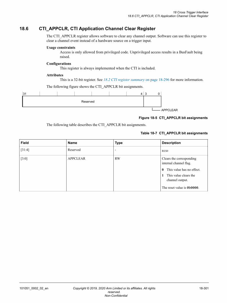
18.6 CTI_APPCLR, CTI Application Channel Clear RegisterThe CTI_APPCLR register allows software to clear any channel output. Software can use this register toclear a channel event instead of a hardware source on a trigger input.
Usage constraintsAccess is only allowed from privileged code. Unprivileged access results in a BusFault beingraised.
ConfigurationsThis register is always implemented when the CTI is included.
AttributesThis is a 32-bit register. See 18.2 CTI register summary on page 18-296 for more information.
The following figure shows the CTI_APPCLR bit assignments.
31 4 3 0
Reserved
APPCLEAR
Figure 18-5 CTI_APPCLR bit assignments
The following table describes the CTI_APPCLR bit assignments.
Table 18-7 CTI_APPCLR bit assignments
Field Name Type Description
[31:4] Reserved - RES0
[3:0] APPCLEAR RW Clears the correspondinginternal channel flag.
0 This value has no effect.
1 This value clears thechannel output.
The reset value is 0b0000.
18 Cross Trigger Interface18.6 CTI_APPCLR, CTI Application Channel Clear Register
101051_0002_02_en Copyright © 2019, 2020 Arm Limited or its affiliates. All rightsreserved.
18-301
Non-Confidential
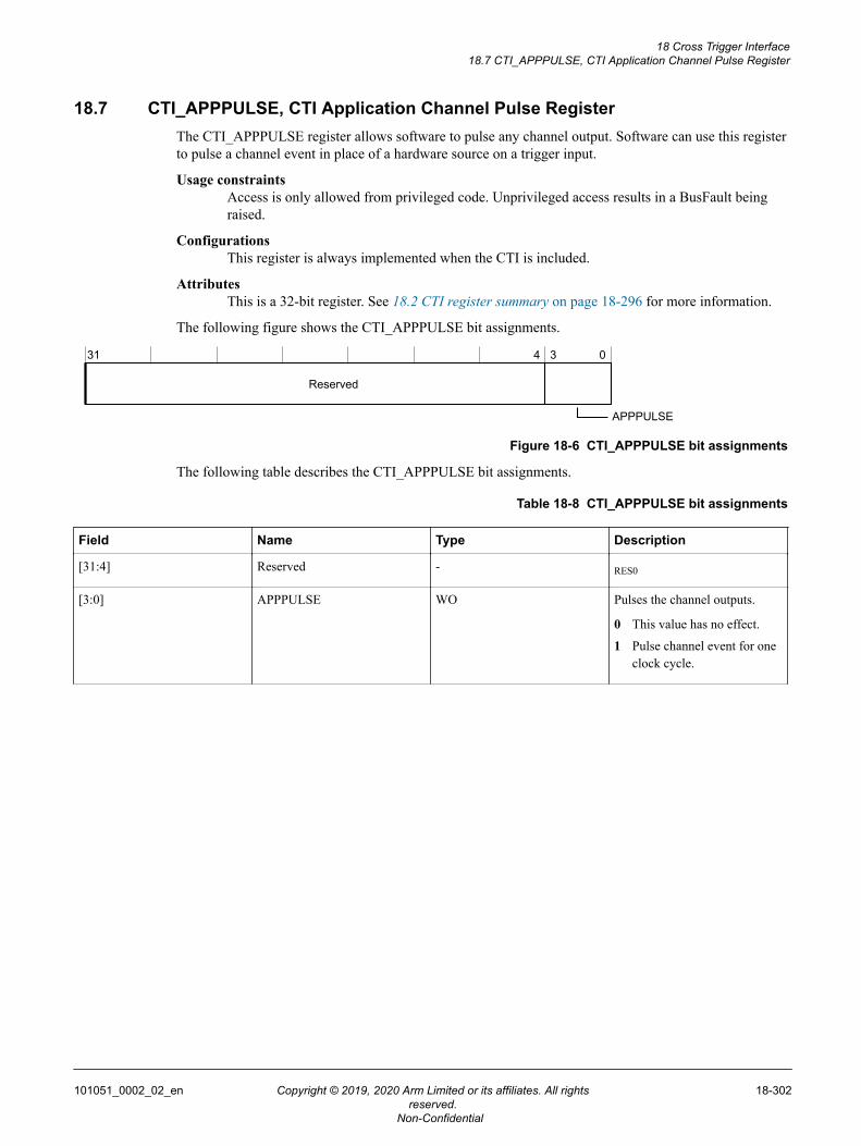
18.7 CTI_APPPULSE, CTI Application Channel Pulse RegisterThe CTI_APPPULSE register allows software to pulse any channel output. Software can use this registerto pulse a channel event in place of a hardware source on a trigger input.
Usage constraintsAccess is only allowed from privileged code. Unprivileged access results in a BusFault beingraised.
ConfigurationsThis register is always implemented when the CTI is included.
AttributesThis is a 32-bit register. See 18.2 CTI register summary on page 18-296 for more information.
The following figure shows the CTI_APPPULSE bit assignments.
31 4 3 0
Reserved
APPPULSE
Figure 18-6 CTI_APPPULSE bit assignments
The following table describes the CTI_APPPULSE bit assignments.
Table 18-8 CTI_APPPULSE bit assignments
Field Name Type Description
[31:4] Reserved - RES0
[3:0] APPPULSE WO Pulses the channel outputs.
0 This value has no effect.
1 Pulse channel event for oneclock cycle.
18 Cross Trigger Interface18.7 CTI_APPPULSE, CTI Application Channel Pulse Register
101051_0002_02_en Copyright © 2019, 2020 Arm Limited or its affiliates. All rightsreserved.
18-302
Non-Confidential
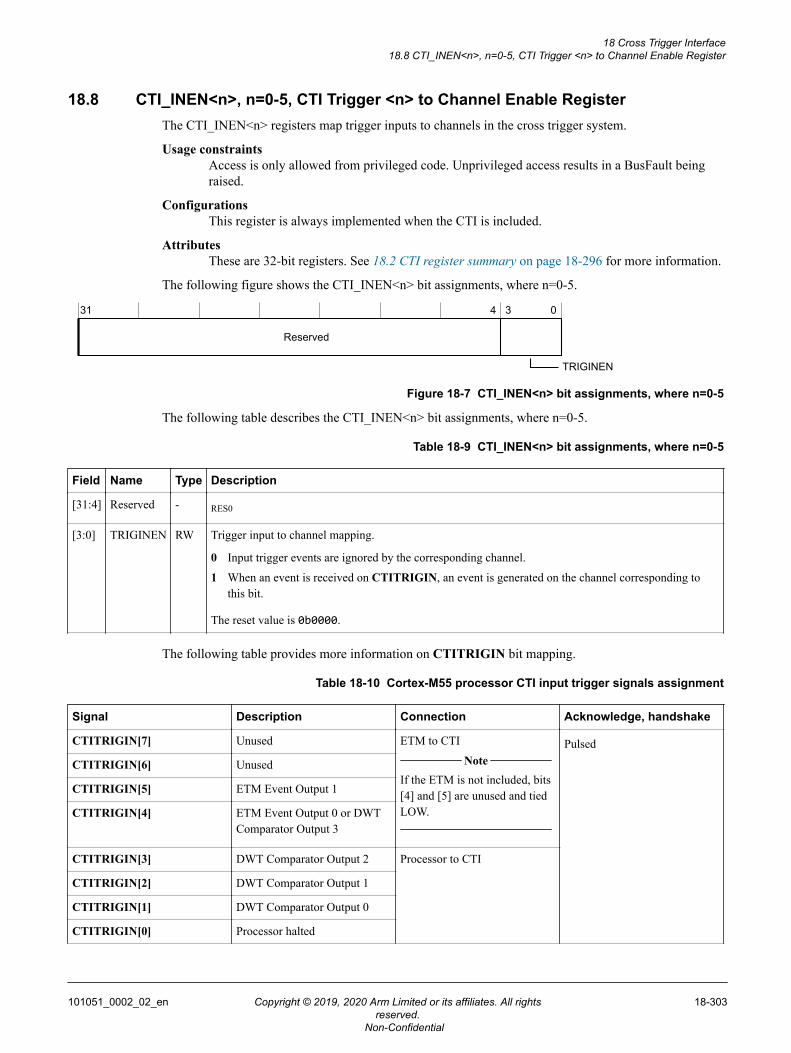
18.8 CTI_INEN<n>, n=0-5, CTI Trigger <n> to Channel Enable RegisterThe CTI_INEN<n> registers map trigger inputs to channels in the cross trigger system.
Usage constraintsAccess is only allowed from privileged code. Unprivileged access results in a BusFault beingraised.
ConfigurationsThis register is always implemented when the CTI is included.
AttributesThese are 32-bit registers. See 18.2 CTI register summary on page 18-296 for more information.
The following figure shows the CTI_INEN<n> bit assignments, where n=0-5.
31 4 3 0
Reserved
TRIGINEN
Figure 18-7 CTI_INEN<n> bit assignments, where n=0-5
The following table describes the CTI_INEN<n> bit assignments, where n=0-5.
Table 18-9 CTI_INEN<n> bit assignments, where n=0-5
Field Name Type Description
[31:4] Reserved - RES0
[3:0] TRIGINEN RW Trigger input to channel mapping.
0 Input trigger events are ignored by the corresponding channel.
1 When an event is received on CTITRIGIN, an event is generated on the channel corresponding tothis bit.
The reset value is 0b0000.
The following table provides more information on CTITRIGIN bit mapping.
Table 18-10 Cortex-M55 processor CTI input trigger signals assignment
Signal Description Connection Acknowledge, handshake
CTITRIGIN[7] Unused ETM to CTI Note
If the ETM is not included, bits[4] and [5] are unused and tiedLOW.
Pulsed
CTITRIGIN[6] Unused
CTITRIGIN[5] ETM Event Output 1
CTITRIGIN[4] ETM Event Output 0 or DWTComparator Output 3
CTITRIGIN[3] DWT Comparator Output 2 Processor to CTI
CTITRIGIN[2] DWT Comparator Output 1
CTITRIGIN[1] DWT Comparator Output 0
CTITRIGIN[0] Processor halted
18 Cross Trigger Interface18.8 CTI_INEN<n>, n=0-5, CTI Trigger <n> to Channel Enable Register
101051_0002_02_en Copyright © 2019, 2020 Arm Limited or its affiliates. All rightsreserved.
18-303
Non-Confidential
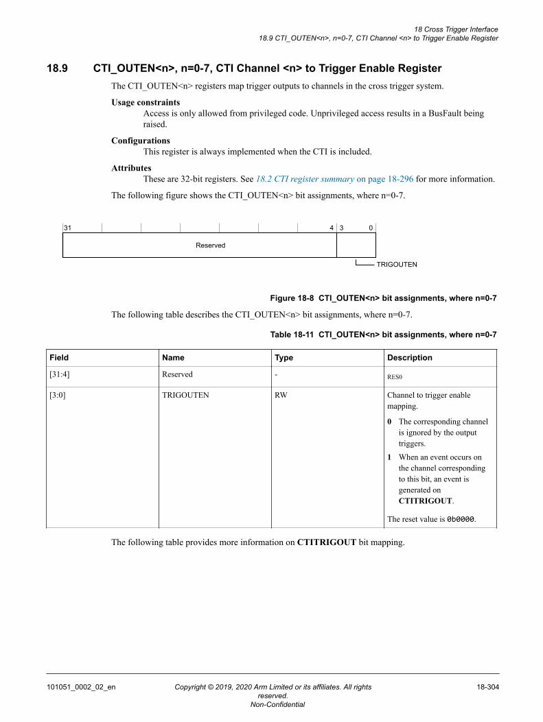
18.9 CTI_OUTEN<n>, n=0-7, CTI Channel <n> to Trigger Enable RegisterThe CTI_OUTEN<n> registers map trigger outputs to channels in the cross trigger system.
Usage constraintsAccess is only allowed from privileged code. Unprivileged access results in a BusFault beingraised.
ConfigurationsThis register is always implemented when the CTI is included.
AttributesThese are 32-bit registers. See 18.2 CTI register summary on page 18-296 for more information.
The following figure shows the CTI_OUTEN<n> bit assignments, where n=0-7.
31 4 3 0
Reserved
TRIGOUTEN
Figure 18-8 CTI_OUTEN<n> bit assignments, where n=0-7
The following table describes the CTI_OUTEN<n> bit assignments, where n=0-7.
Table 18-11 CTI_OUTEN<n> bit assignments, where n=0-7
Field Name Type Description
[31:4] Reserved - RES0
[3:0] TRIGOUTEN RW Channel to trigger enablemapping.
0 The corresponding channelis ignored by the outputtriggers.
1 When an event occurs onthe channel correspondingto this bit, an event isgenerated onCTITRIGOUT.
The reset value is 0b0000.
The following table provides more information on CTITRIGOUT bit mapping.
18 Cross Trigger Interface18.9 CTI_OUTEN<n>, n=0-7, CTI Channel <n> to Trigger Enable Register
101051_0002_02_en Copyright © 2019, 2020 Arm Limited or its affiliates. All rightsreserved.
18-304
Non-Confidential
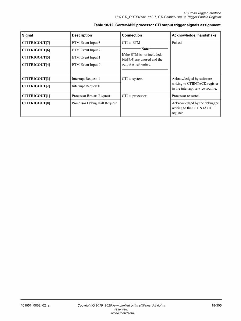
Table 18-12 Cortex-M55 processor CTI output trigger signals assignment
Signal Description Connection Acknowledge, handshake
CTITRIGOUT[7] ETM Event Input 3 CTI to ETM Note
If the ETM is not included,bits[7:4] are unused and theoutput is left untied.
Pulsed
CTITRIGOUT[6] ETM Event Input 2
CTITRIGOUT[5] ETM Event Input 1
CTITRIGOUT[4] ETM Event Input 0
CTITRIGOUT[3] Interrupt Request 1 CTI to system Acknowledged by softwarewriting to CTIINTACK registerin the interrupt service routine.CTITRIGOUT[2] Interrupt Request 0
CTITRIGOUT[1] Processor Restart Request CTI to processor Processor restarted
CTITRIGOUT[0] Processor Debug Halt Request Acknowledged by the debuggerwriting to the CTIINTACKregister.
18 Cross Trigger Interface18.9 CTI_OUTEN<n>, n=0-7, CTI Channel <n> to Trigger Enable Register
101051_0002_02_en Copyright © 2019, 2020 Arm Limited or its affiliates. All rightsreserved.
18-305
Non-Confidential
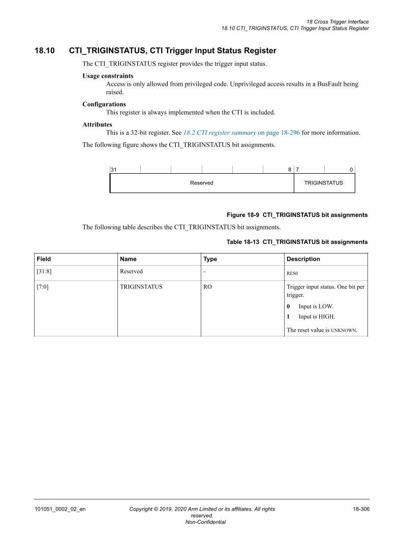
18.10 CTI_TRIGINSTATUS, CTI Trigger Input Status RegisterThe CTI_TRIGINSTATUS register provides the trigger input status.
Usage constraintsAccess is only allowed from privileged code. Unprivileged access results in a BusFault beingraised.
ConfigurationsThis register is always implemented when the CTI is included.
AttributesThis is a 32-bit register. See 18.2 CTI register summary on page 18-296 for more information.
The following figure shows the CTI_TRIGINSTATUS bit assignments.
31 8 7 0
Reserved TRIGINSTATUS
Figure 18-9 CTI_TRIGINSTATUS bit assignments
The following table describes the CTI_TRIGINSTATUS bit assignments.
Table 18-13 CTI_TRIGINSTATUS bit assignments
Field Name Type Description
[31:8] Reserved - RES0
[7:0] TRIGINSTATUS RO Trigger input status. One bit pertrigger.
0 Input is LOW.
1 Input is HIGH.
The reset value is UNKNOWN.
18 Cross Trigger Interface18.10 CTI_TRIGINSTATUS, CTI Trigger Input Status Register
101051_0002_02_en Copyright © 2019, 2020 Arm Limited or its affiliates. All rightsreserved.
18-306
Non-Confidential
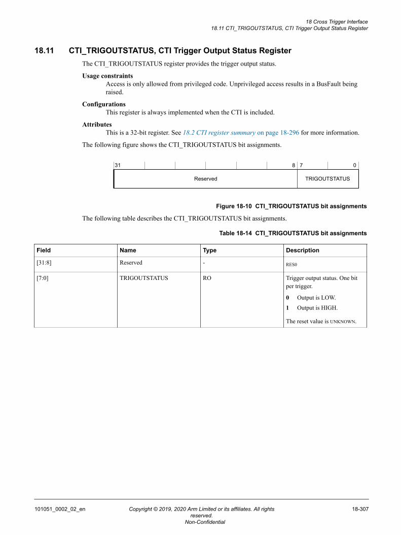
18.11 CTI_TRIGOUTSTATUS, CTI Trigger Output Status RegisterThe CTI_TRIGOUTSTATUS register provides the trigger output status.
Usage constraintsAccess is only allowed from privileged code. Unprivileged access results in a BusFault beingraised.
ConfigurationsThis register is always implemented when the CTI is included.
AttributesThis is a 32-bit register. See 18.2 CTI register summary on page 18-296 for more information.
The following figure shows the CTI_TRIGOUTSTATUS bit assignments.
31 07
Reserved
8
TRIGOUTSTATUS
Figure 18-10 CTI_TRIGOUTSTATUS bit assignments
The following table describes the CTI_TRIGOUTSTATUS bit assignments.
Table 18-14 CTI_TRIGOUTSTATUS bit assignments
Field Name Type Description
[31:8] Reserved - RES0
[7:0] TRIGOUTSTATUS RO Trigger output status. One bitper trigger.
0 Output is LOW.
1 Output is HIGH.
The reset value is UNKNOWN.
18 Cross Trigger Interface18.11 CTI_TRIGOUTSTATUS, CTI Trigger Output Status Register
101051_0002_02_en Copyright © 2019, 2020 Arm Limited or its affiliates. All rightsreserved.
18-307
Non-Confidential
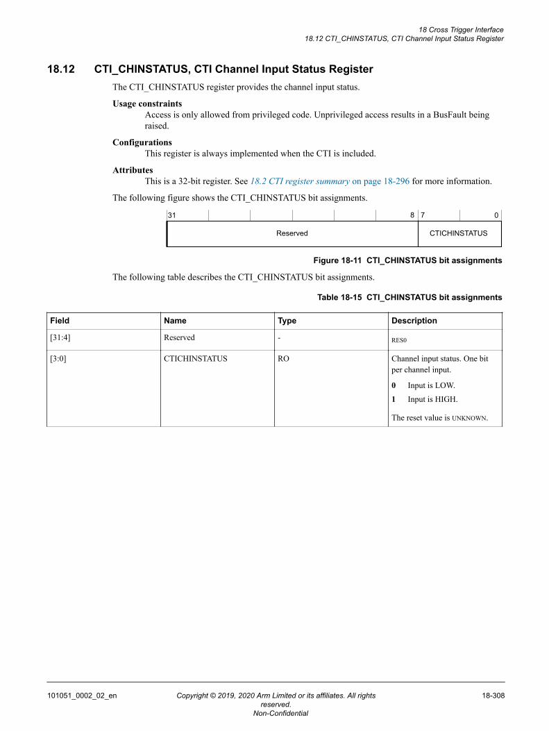
18.12 CTI_CHINSTATUS, CTI Channel Input Status RegisterThe CTI_CHINSTATUS register provides the channel input status.
Usage constraintsAccess is only allowed from privileged code. Unprivileged access results in a BusFault beingraised.
ConfigurationsThis register is always implemented when the CTI is included.
AttributesThis is a 32-bit register. See 18.2 CTI register summary on page 18-296 for more information.
The following figure shows the CTI_CHINSTATUS bit assignments.
31 8 7 0
Reserved CTICHINSTATUS
Figure 18-11 CTI_CHINSTATUS bit assignments
The following table describes the CTI_CHINSTATUS bit assignments.
Table 18-15 CTI_CHINSTATUS bit assignments
Field Name Type Description
[31:4] Reserved - RES0
[3:0] CTICHINSTATUS RO Channel input status. One bitper channel input.
0 Input is LOW.
1 Input is HIGH.
The reset value is UNKNOWN.
18 Cross Trigger Interface18.12 CTI_CHINSTATUS, CTI Channel Input Status Register
101051_0002_02_en Copyright © 2019, 2020 Arm Limited or its affiliates. All rightsreserved.
18-308
Non-Confidential
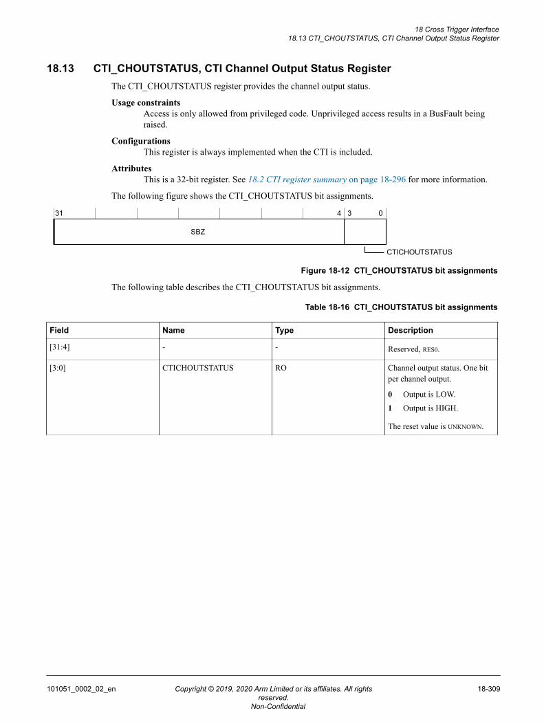
18.13 CTI_CHOUTSTATUS, CTI Channel Output Status RegisterThe CTI_CHOUTSTATUS register provides the channel output status.
Usage constraintsAccess is only allowed from privileged code. Unprivileged access results in a BusFault beingraised.
ConfigurationsThis register is always implemented when the CTI is included.
AttributesThis is a 32-bit register. See 18.2 CTI register summary on page 18-296 for more information.
The following figure shows the CTI_CHOUTSTATUS bit assignments.
31 4 3 0
SBZ
CTICHOUTSTATUS
Figure 18-12 CTI_CHOUTSTATUS bit assignments
The following table describes the CTI_CHOUTSTATUS bit assignments.
Table 18-16 CTI_CHOUTSTATUS bit assignments
Field Name Type Description
[31:4] - - Reserved, RES0.
[3:0] CTICHOUTSTATUS RO Channel output status. One bitper channel output.
0 Output is LOW.
1 Output is HIGH.
The reset value is UNKNOWN.
18 Cross Trigger Interface18.13 CTI_CHOUTSTATUS, CTI Channel Output Status Register
101051_0002_02_en Copyright © 2019, 2020 Arm Limited or its affiliates. All rightsreserved.
18-309
Non-Confidential
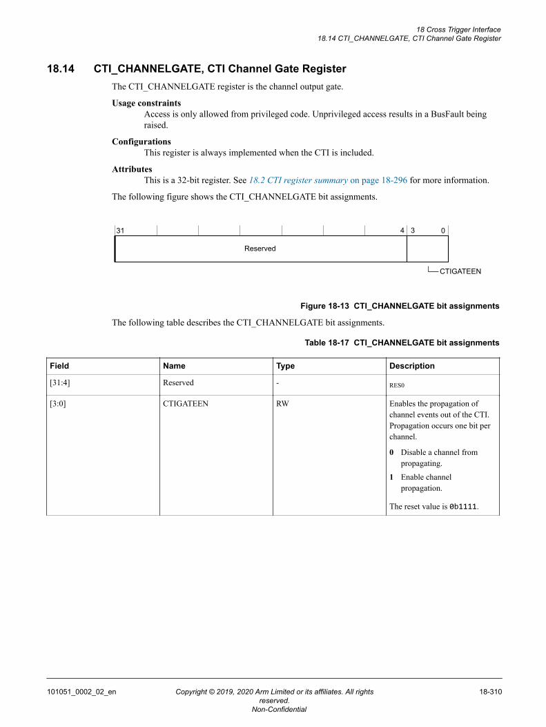
18.14 CTI_CHANNELGATE, CTI Channel Gate RegisterThe CTI_CHANNELGATE register is the channel output gate.
Usage constraintsAccess is only allowed from privileged code. Unprivileged access results in a BusFault beingraised.
ConfigurationsThis register is always implemented when the CTI is included.
AttributesThis is a 32-bit register. See 18.2 CTI register summary on page 18-296 for more information.
The following figure shows the CTI_CHANNELGATE bit assignments.
31 4 3 0
Reserved
CTIGATEEN
Figure 18-13 CTI_CHANNELGATE bit assignments
The following table describes the CTI_CHANNELGATE bit assignments.
Table 18-17 CTI_CHANNELGATE bit assignments
Field Name Type Description
[31:4] Reserved - RES0
[3:0] CTIGATEEN RW Enables the propagation ofchannel events out of the CTI.Propagation occurs one bit perchannel.
0 Disable a channel frompropagating.
1 Enable channelpropagation.
The reset value is 0b1111.
18 Cross Trigger Interface18.14 CTI_CHANNELGATE, CTI Channel Gate Register
101051_0002_02_en Copyright © 2019, 2020 Arm Limited or its affiliates. All rightsreserved.
18-310
Non-Confidential
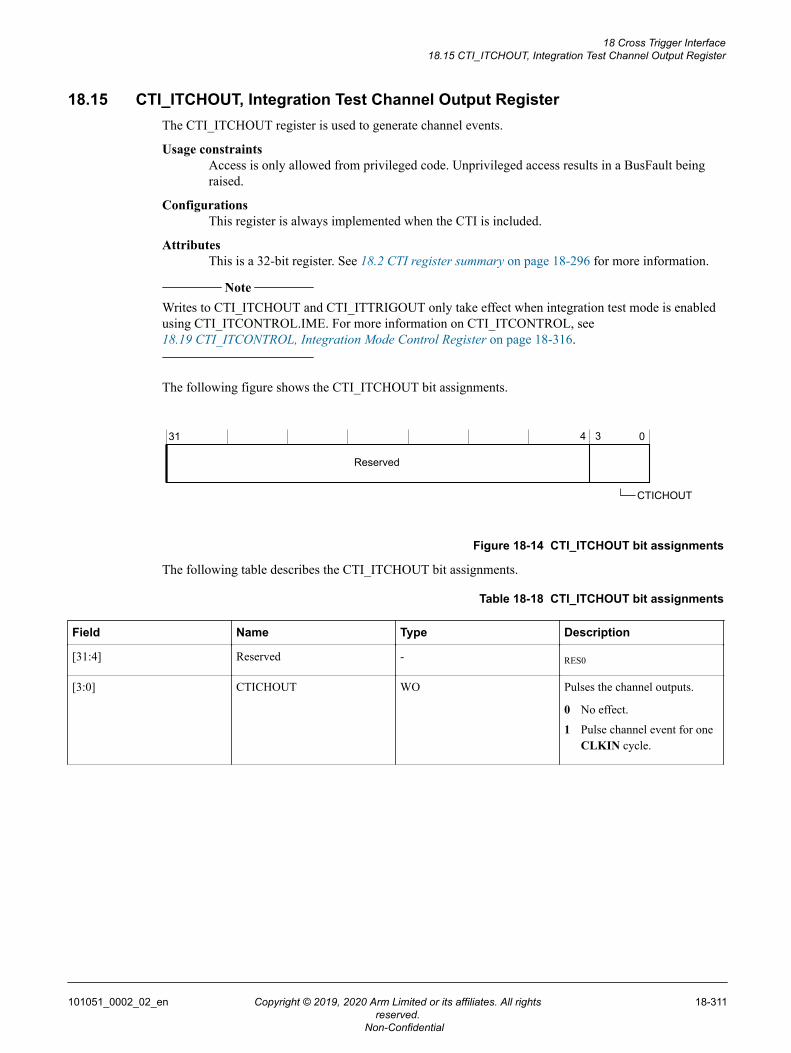
18.15 CTI_ITCHOUT, Integration Test Channel Output RegisterThe CTI_ITCHOUT register is used to generate channel events.
Usage constraintsAccess is only allowed from privileged code. Unprivileged access results in a BusFault beingraised.
ConfigurationsThis register is always implemented when the CTI is included.
AttributesThis is a 32-bit register. See 18.2 CTI register summary on page 18-296 for more information.
Note
Writes to CTI_ITCHOUT and CTI_ITTRIGOUT only take effect when integration test mode is enabledusing CTI_ITCONTROL.IME. For more information on CTI_ITCONTROL, see18.19 CTI_ITCONTROL, Integration Mode Control Register on page 18-316.
The following figure shows the CTI_ITCHOUT bit assignments.
31 4 3 0
Reserved
CTICHOUT
Figure 18-14 CTI_ITCHOUT bit assignments
The following table describes the CTI_ITCHOUT bit assignments.
Table 18-18 CTI_ITCHOUT bit assignments
Field Name Type Description
[31:4] Reserved - RES0
[3:0] CTICHOUT WO Pulses the channel outputs.
0 No effect.
1 Pulse channel event for oneCLKIN cycle.
18 Cross Trigger Interface18.15 CTI_ITCHOUT, Integration Test Channel Output Register
101051_0002_02_en Copyright © 2019, 2020 Arm Limited or its affiliates. All rightsreserved.
18-311
Non-Confidential
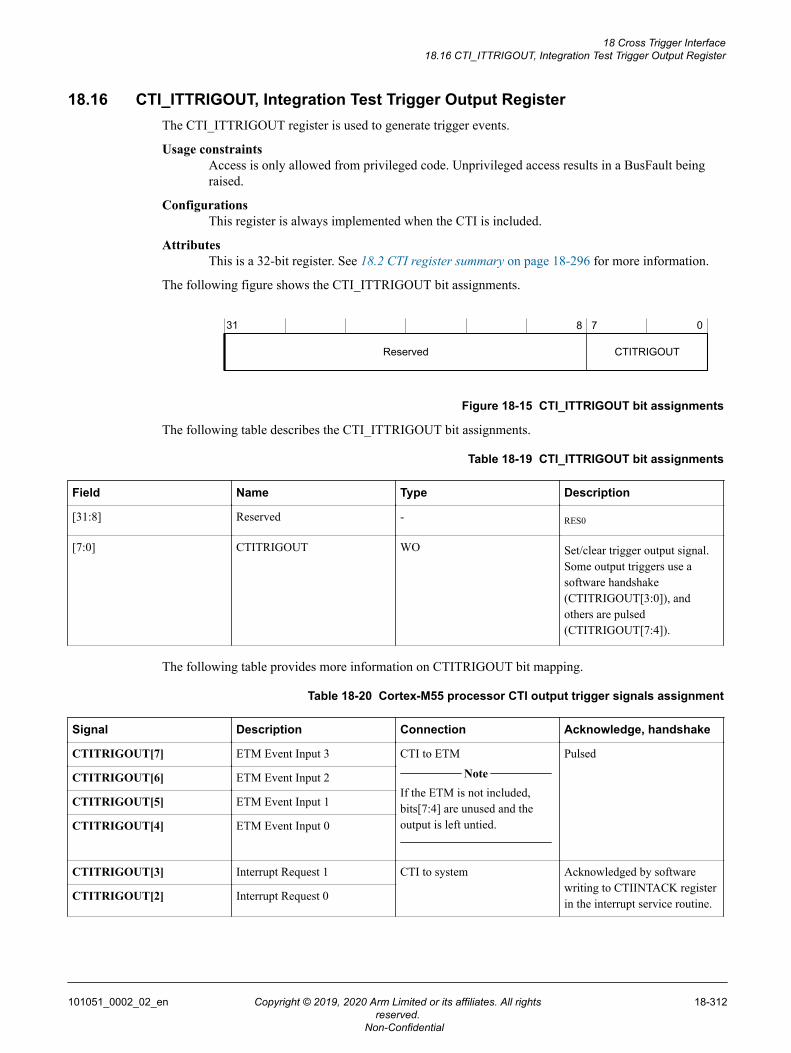
18.16 CTI_ITTRIGOUT, Integration Test Trigger Output RegisterThe CTI_ITTRIGOUT register is used to generate trigger events.
Usage constraintsAccess is only allowed from privileged code. Unprivileged access results in a BusFault beingraised.
ConfigurationsThis register is always implemented when the CTI is included.
AttributesThis is a 32-bit register. See 18.2 CTI register summary on page 18-296 for more information.
The following figure shows the CTI_ITTRIGOUT bit assignments.
31 07
Reserved
8
CTITRIGOUT
Figure 18-15 CTI_ITTRIGOUT bit assignments
The following table describes the CTI_ITTRIGOUT bit assignments.
Table 18-19 CTI_ITTRIGOUT bit assignments
Field Name Type Description
[31:8] Reserved - RES0
[7:0] CTITRIGOUT WO Set/clear trigger output signal.Some output triggers use asoftware handshake(CTITRIGOUT[3:0]), andothers are pulsed(CTITRIGOUT[7:4]).
The following table provides more information on CTITRIGOUT bit mapping.
Table 18-20 Cortex-M55 processor CTI output trigger signals assignment
Signal Description Connection Acknowledge, handshake
CTITRIGOUT[7] ETM Event Input 3 CTI to ETM Note
If the ETM is not included,bits[7:4] are unused and theoutput is left untied.
Pulsed
CTITRIGOUT[6] ETM Event Input 2
CTITRIGOUT[5] ETM Event Input 1
CTITRIGOUT[4] ETM Event Input 0
CTITRIGOUT[3] Interrupt Request 1 CTI to system Acknowledged by softwarewriting to CTIINTACK registerin the interrupt service routine.CTITRIGOUT[2] Interrupt Request 0
18 Cross Trigger Interface18.16 CTI_ITTRIGOUT, Integration Test Trigger Output Register
101051_0002_02_en Copyright © 2019, 2020 Arm Limited or its affiliates. All rightsreserved.
18-312
Non-Confidential
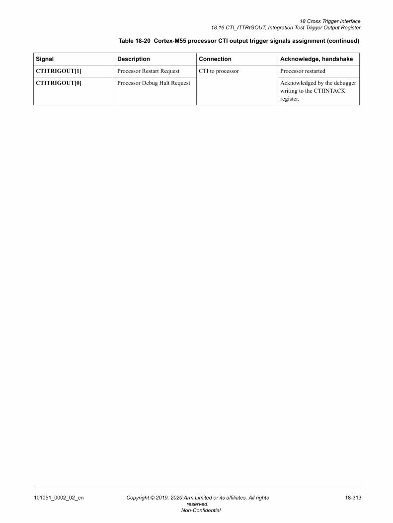
Table 18-20 Cortex-M55 processor CTI output trigger signals assignment (continued)
Signal Description Connection Acknowledge, handshake
CTITRIGOUT[1] Processor Restart Request CTI to processor Processor restarted
CTITRIGOUT[0] Processor Debug Halt Request Acknowledged by the debuggerwriting to the CTIINTACKregister.
18 Cross Trigger Interface18.16 CTI_ITTRIGOUT, Integration Test Trigger Output Register
101051_0002_02_en Copyright © 2019, 2020 Arm Limited or its affiliates. All rightsreserved.
18-313
Non-Confidential
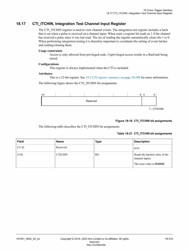
18.17 CTI_ITCHIN, Integration Test Channel Input RegisterThe CTI_ITCHIN register is used to view channel events. The integration test register includes a latchthat is set when a pulse is received on a channel input. When read, a register bit reads as 1 if the channelhas received a pulse since it was last read. The act of reading the register automatically clears the 1 to 0.When performing integration testing it is therefore important to coordinate the setting of event latchesand reading/clearing them.
Usage constraintsAccess is only allowed from privileged code. Unprivileged access results in a BusFault beingraised.
ConfigurationsThis register is always implemented when the CTI is included.
AttributesThis is a 32-bit register. See 18.2 CTI register summary on page 18-296 for more information.
The following figure shows the CTI_ITCHIN bit assignments.
31 4 3 0
Reserved
CTICHIN
Figure 18-16 CTI_ITCHIN bit assignments
The following table describes the CTI_ITCHIN bit assignments.
Table 18-21 CTI_ITCHIN bit assignments
Field Name Type Description
[31:4] Reserved - RES0
[3:0] CTICHIN RO Reads the latched value of thechannel inputs.
The reset value is 0b0000.
18 Cross Trigger Interface18.17 CTI_ITCHIN, Integration Test Channel Input Register
101051_0002_02_en Copyright © 2019, 2020 Arm Limited or its affiliates. All rightsreserved.
18-314
Non-Confidential
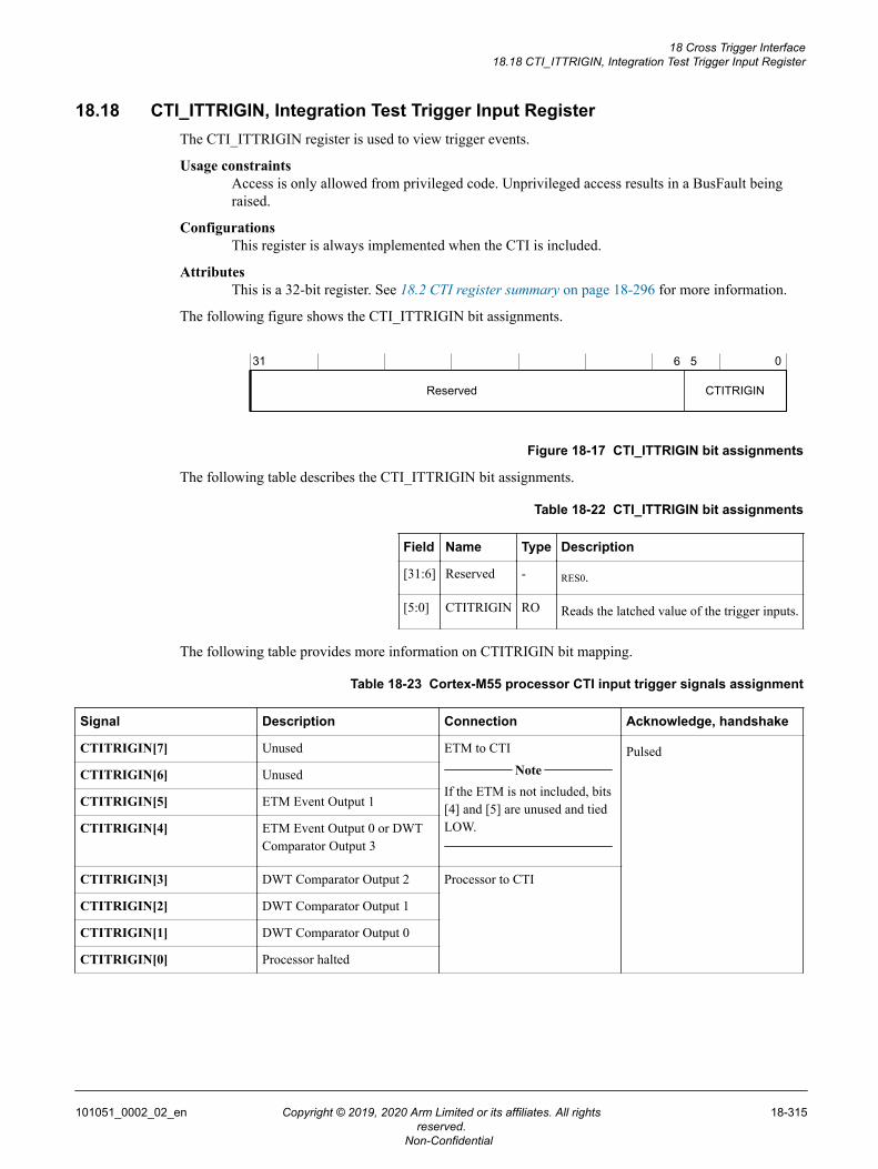
18.18 CTI_ITTRIGIN, Integration Test Trigger Input RegisterThe CTI_ITTRIGIN register is used to view trigger events.
Usage constraintsAccess is only allowed from privileged code. Unprivileged access results in a BusFault beingraised.
ConfigurationsThis register is always implemented when the CTI is included.
AttributesThis is a 32-bit register. See 18.2 CTI register summary on page 18-296 for more information.
The following figure shows the CTI_ITTRIGIN bit assignments.
31 05
Reserved
6
CTITRIGIN
Figure 18-17 CTI_ITTRIGIN bit assignments
The following table describes the CTI_ITTRIGIN bit assignments.
Table 18-22 CTI_ITTRIGIN bit assignments
Field Name Type Description
[31:6] Reserved - RES0.
[5:0] CTITRIGIN RO Reads the latched value of the trigger inputs.
The following table provides more information on CTITRIGIN bit mapping.
Table 18-23 Cortex-M55 processor CTI input trigger signals assignment
Signal Description Connection Acknowledge, handshake
CTITRIGIN[7] Unused ETM to CTI Note
If the ETM is not included, bits[4] and [5] are unused and tiedLOW.
Pulsed
CTITRIGIN[6] Unused
CTITRIGIN[5] ETM Event Output 1
CTITRIGIN[4] ETM Event Output 0 or DWTComparator Output 3
CTITRIGIN[3] DWT Comparator Output 2 Processor to CTI
CTITRIGIN[2] DWT Comparator Output 1
CTITRIGIN[1] DWT Comparator Output 0
CTITRIGIN[0] Processor halted
18 Cross Trigger Interface18.18 CTI_ITTRIGIN, Integration Test Trigger Input Register
101051_0002_02_en Copyright © 2019, 2020 Arm Limited or its affiliates. All rightsreserved.
18-315
Non-Confidential
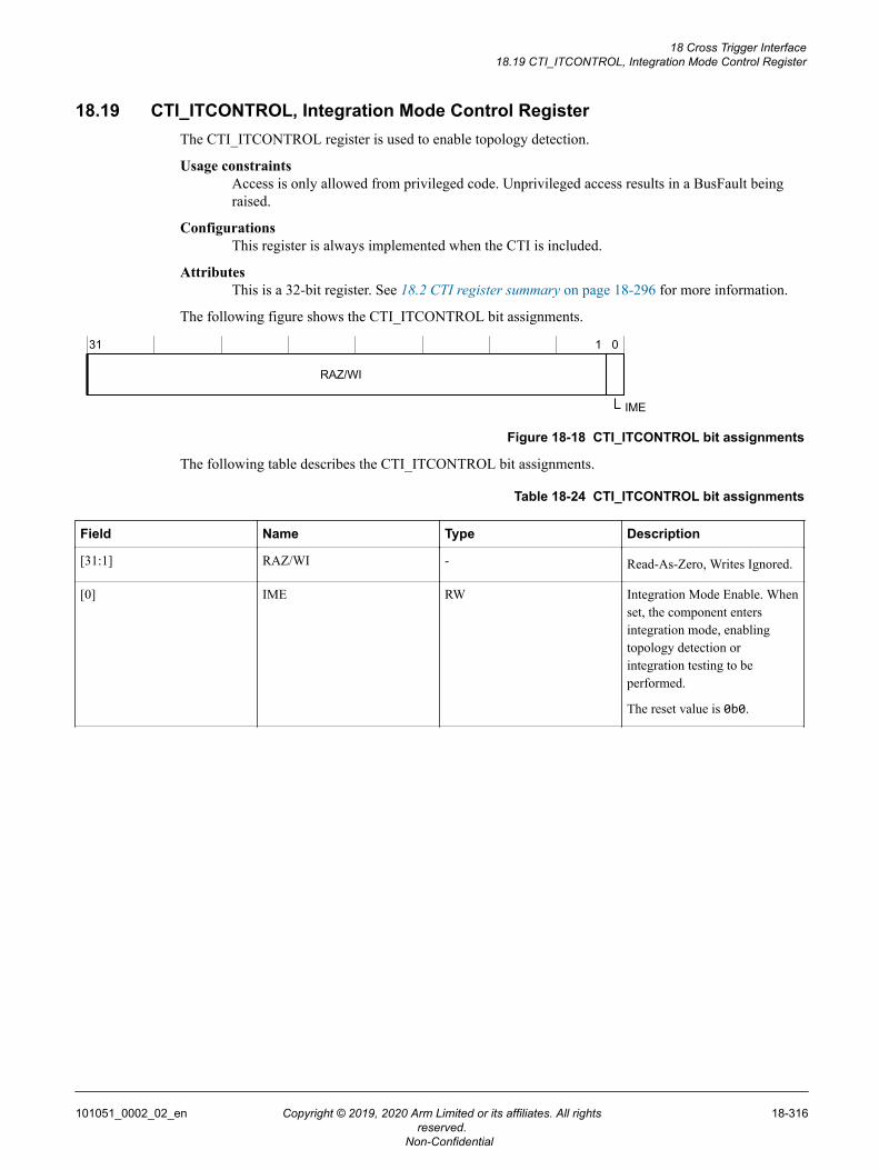
18.19 CTI_ITCONTROL, Integration Mode Control RegisterThe CTI_ITCONTROL register is used to enable topology detection.
Usage constraintsAccess is only allowed from privileged code. Unprivileged access results in a BusFault beingraised.
ConfigurationsThis register is always implemented when the CTI is included.
AttributesThis is a 32-bit register. See 18.2 CTI register summary on page 18-296 for more information.
The following figure shows the CTI_ITCONTROL bit assignments.
31 1 0
RAZ/WI
IME
Figure 18-18 CTI_ITCONTROL bit assignments
The following table describes the CTI_ITCONTROL bit assignments.
Table 18-24 CTI_ITCONTROL bit assignments
Field Name Type Description
[31:1] RAZ/WI - Read-As-Zero, Writes Ignored.
[0] IME RW Integration Mode Enable. Whenset, the component entersintegration mode, enablingtopology detection orintegration testing to beperformed.
The reset value is 0b0.
18 Cross Trigger Interface18.19 CTI_ITCONTROL, Integration Mode Control Register
101051_0002_02_en Copyright © 2019, 2020 Arm Limited or its affiliates. All rightsreserved.
18-316
Non-Confidential
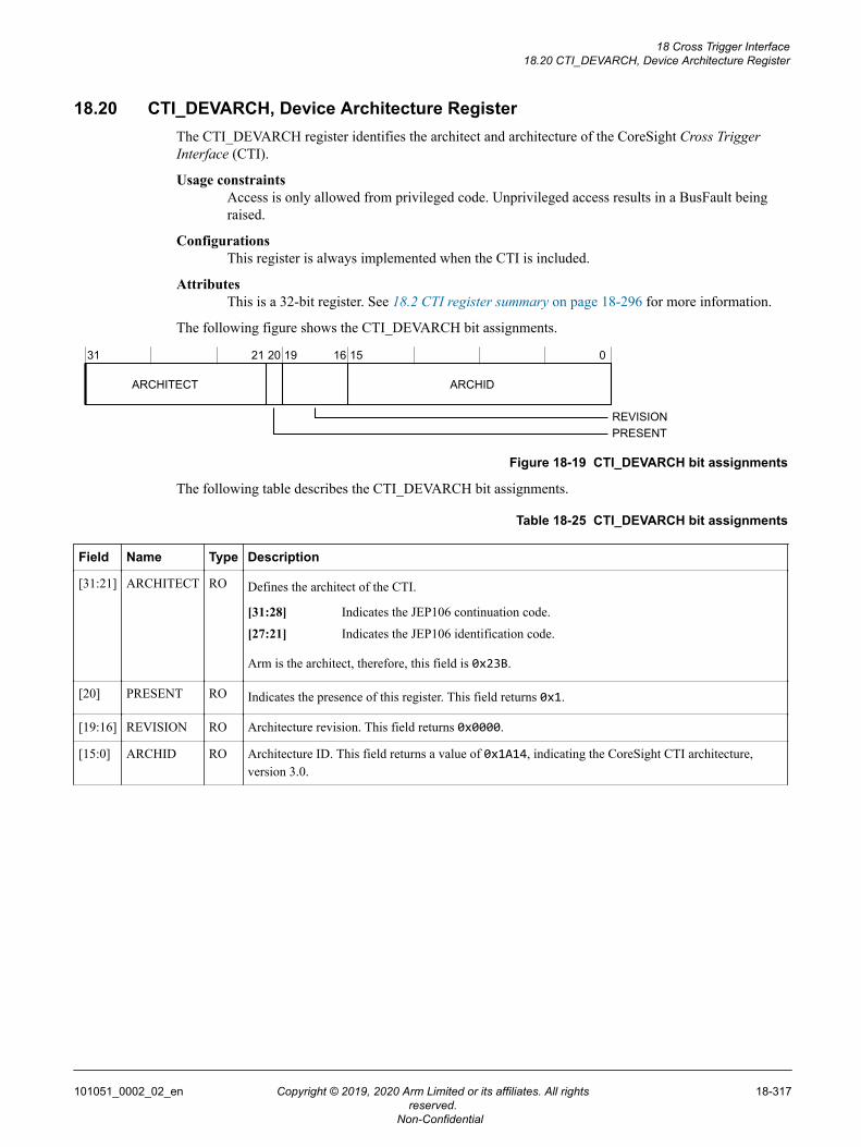
18.20 CTI_DEVARCH, Device Architecture RegisterThe CTI_DEVARCH register identifies the architect and architecture of the CoreSight Cross TriggerInterface (CTI).
Usage constraintsAccess is only allowed from privileged code. Unprivileged access results in a BusFault beingraised.
ConfigurationsThis register is always implemented when the CTI is included.
AttributesThis is a 32-bit register. See 18.2 CTI register summary on page 18-296 for more information.
The following figure shows the CTI_DEVARCH bit assignments.
31 21 20 19 16 15 0
ARCHIDARCHITECT
PRESENTREVISION
Figure 18-19 CTI_DEVARCH bit assignments
The following table describes the CTI_DEVARCH bit assignments.
Table 18-25 CTI_DEVARCH bit assignments
Field Name Type Description
[31:21] ARCHITECT RO Defines the architect of the CTI.
[31:28] Indicates the JEP106 continuation code.
[27:21] Indicates the JEP106 identification code.
Arm is the architect, therefore, this field is 0x23B.
[20] PRESENT RO Indicates the presence of this register. This field returns 0x1.
[19:16] REVISION RO Architecture revision. This field returns 0x0000.
[15:0] ARCHID RO Architecture ID. This field returns a value of 0x1A14, indicating the CoreSight CTI architecture,version 3.0.
18 Cross Trigger Interface18.20 CTI_DEVARCH, Device Architecture Register
101051_0002_02_en Copyright © 2019, 2020 Arm Limited or its affiliates. All rightsreserved.
18-317
Non-Confidential
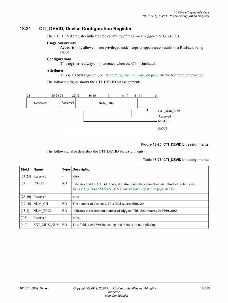
18.21 CTI_DEVID, Device Configuration RegisterThe CTI_DEVID register indicates the capability of the Cross Trigger Interface (CTI).
Usage constraintsAccess is only allowed from privileged code. Unprivileged access results in a BusFault beingraised.
ConfigurationsThis register is always implemented when the CTI is included.
AttributesThis is a 32-bit register. See 18.2 CTI register summary on page 18-296 for more information.
The following figure shows the CTI_DEVID bit assignments.
31 25 24 23 20 19 16 15 8 7 5 4 0
Reserved
NUM_TRIGReservedReserved
INOUT
NUM_CH
EXT_MUX_NUM
Figure 18-20 CTI_DEVID bit assignments
The following table describes the CTI_DEVID bit assignments.
Table 18-26 CTI_DEVID bit assignments
Field Name Type Description
[31:25] Reserved - RES0.
[24] INOUT RO Indicates that the CTIGATE register also masks the channel inputs. This field returns 0b0.18.14 CTI_CHANNELGATE, CTI Channel Gate Register on page 18-310.
[23:20] Reserved - RES0.
[19:16] NUM_CH RO The number of channels. This field returns 0b0100.
[15:8] NUM_TRIG RO Indicates the maximum number of triggers. This field returns 0b00001000.
[7:5] Reserved - RES0.
[4:0] EXT_MUX_NUM RO This field is 0b0000 indicating that there is no multiplexing.
18 Cross Trigger Interface18.21 CTI_DEVID, Device Configuration Register
101051_0002_02_en Copyright © 2019, 2020 Arm Limited or its affiliates. All rightsreserved.
18-318
Non-Confidential
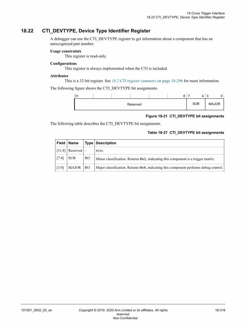
18.22 CTI_DEVTYPE, Device Type Identifier RegisterA debugger can use the CTI_DEVTYPE register to get information about a component that has anunrecognized part number.
Usage constraintsThis register is read-only.
ConfigurationsThis register is always implemented when the CTI is included.
AttributesThis is a 32-bit register. See 18.2 CTI register summary on page 18-296 for more information.
The following figure shows the CTI_DEVTYPE bit assignments.
31 8 7 4 3 0
MAJORSUBReserved
Figure 18-21 CTI_DEVTYPE bit assignments
The following table describes the CTI_DEVTYPE bit assignments.
Table 18-27 CTI_DEVTYPE bit assignments
Field Name Type Description
[31:8] Reserved - RES0.
[7:4] SUB RO Minor classification. Returns 0x1, indicating this component is a trigger matrix.
[3:0] MAJOR RO Major classification. Returns 0x4, indicating this component performs debug control.
18 Cross Trigger Interface18.22 CTI_DEVTYPE, Device Type Identifier Register
101051_0002_02_en Copyright © 2019, 2020 Arm Limited or its affiliates. All rightsreserved.
18-319
Non-Confidential
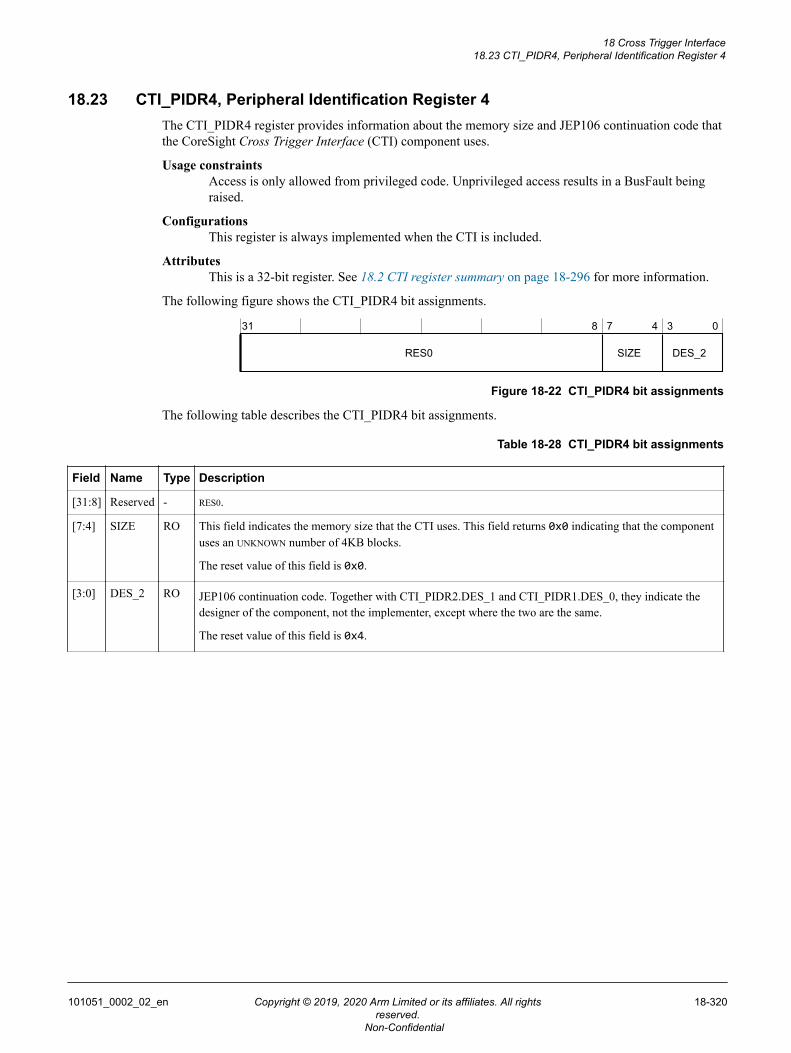
18.23 CTI_PIDR4, Peripheral Identification Register 4The CTI_PIDR4 register provides information about the memory size and JEP106 continuation code thatthe CoreSight Cross Trigger Interface (CTI) component uses.
Usage constraintsAccess is only allowed from privileged code. Unprivileged access results in a BusFault beingraised.
ConfigurationsThis register is always implemented when the CTI is included.
AttributesThis is a 32-bit register. See 18.2 CTI register summary on page 18-296 for more information.
The following figure shows the CTI_PIDR4 bit assignments.
31 8 7 4 3 0
DES_2SIZERES0
Figure 18-22 CTI_PIDR4 bit assignments
The following table describes the CTI_PIDR4 bit assignments.
Table 18-28 CTI_PIDR4 bit assignments
Field Name Type Description
[31:8] Reserved - RES0.
[7:4] SIZE RO This field indicates the memory size that the CTI uses. This field returns 0x0 indicating that the componentuses an UNKNOWN number of 4KB blocks.
The reset value of this field is 0x0.
[3:0] DES_2 RO JEP106 continuation code. Together with CTI_PIDR2.DES_1 and CTI_PIDR1.DES_0, they indicate thedesigner of the component, not the implementer, except where the two are the same.
The reset value of this field is 0x4.
18 Cross Trigger Interface18.23 CTI_PIDR4, Peripheral Identification Register 4
101051_0002_02_en Copyright © 2019, 2020 Arm Limited or its affiliates. All rightsreserved.
18-320
Non-Confidential

18.24 CTI_PIDR5, Peripheral Identification Register 5The CTI_PIDR5 register is reserved.
Usage constraintsAccess is only allowed from privileged code. Unprivileged access results in a BusFault beingraised.
ConfigurationsThis register is always implemented when the CTI is included.
AttributesThis is a 32-bit register. See 18.2 CTI register summary on page 18-296 for more information.
The following figure shows the CTI_PIDR5 bit assignments.
31 8 7 0
Reserved PIDR5
Figure 18-23 CTI_PIDR5 bit assignments
The following table describes the CTI_PIDR5 bit assignments.
Table 18-29 CTI_PIDR5 bit assignments
Field Name Type Description
[31:8] Reserved - RES0.
[7:0] PIDR5 RO RES0.
18 Cross Trigger Interface18.24 CTI_PIDR5, Peripheral Identification Register 5
101051_0002_02_en Copyright © 2019, 2020 Arm Limited or its affiliates. All rightsreserved.
18-321
Non-Confidential
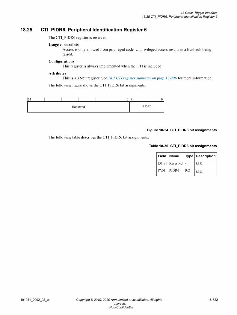
18.25 CTI_PIDR6, Peripheral Identification Register 6The CTI_PIDR6 register is reserved.
Usage constraintsAccess is only allowed from privileged code. Unprivileged access results in a BusFault beingraised.
ConfigurationsThis register is always implemented when the CTI is included.
AttributesThis is a 32-bit register. See 18.2 CTI register summary on page 18-296 for more information.
The following figure shows the CTI_PIDR6 bit assignments.
31 8 7 0
Reserved PIDR6
Figure 18-24 CTI_PIDR6 bit assignments
The following table describes the CTI_PIDR6 bit assignments.
Table 18-30 CTI_PIDR6 bit assignments
Field Name Type Description
[31:8] Reserved - RES0.
[7:0] PIDR6 RO RES0.
18 Cross Trigger Interface18.25 CTI_PIDR6, Peripheral Identification Register 6
101051_0002_02_en Copyright © 2019, 2020 Arm Limited or its affiliates. All rightsreserved.
18-322
Non-Confidential

18.26 CTI_PIDR7, Peripheral Identification Register 7The CTI_PIDR7 register is reserved.
Usage constraintsAccess is only allowed from privileged code. Unprivileged access results in a BusFault beingraised.
ConfigurationsThis register is always implemented when the CTI is included.
AttributesThis is a 32-bit register. See 18.2 CTI register summary on page 18-296 for more information.
The following figure shows the CTI_PIDR7 bit assignments.
31 8 7 0
Reserved PIDR7
Figure 18-25 CTI_PIDR7 bit assignments
The following table describes the CTI_PIDR7 bit assignments.
Table 18-31 CTI_PIDR7 bit assignments
Field Name Type Description
[31:8] Reserved - RES0.
[7:0] PIDR7 RO RES0.
18 Cross Trigger Interface18.26 CTI_PIDR7, Peripheral Identification Register 7
101051_0002_02_en Copyright © 2019, 2020 Arm Limited or its affiliates. All rightsreserved.
18-323
Non-Confidential
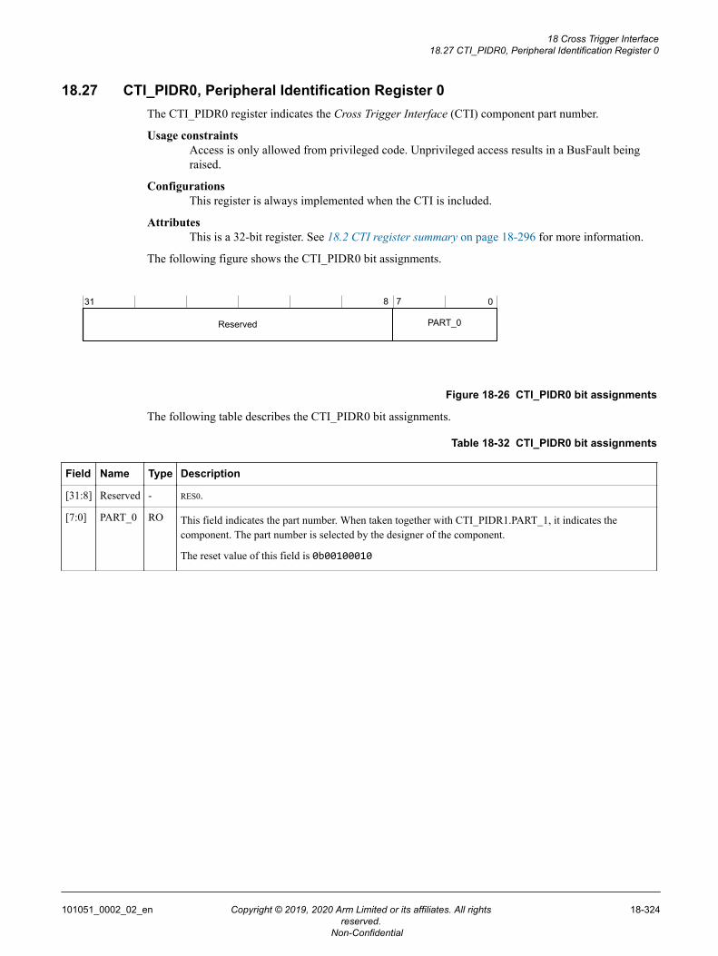
18.27 CTI_PIDR0, Peripheral Identification Register 0The CTI_PIDR0 register indicates the Cross Trigger Interface (CTI) component part number.
Usage constraintsAccess is only allowed from privileged code. Unprivileged access results in a BusFault beingraised.
ConfigurationsThis register is always implemented when the CTI is included.
AttributesThis is a 32-bit register. See 18.2 CTI register summary on page 18-296 for more information.
The following figure shows the CTI_PIDR0 bit assignments.
31 8 7 0
Reserved PART_0
Figure 18-26 CTI_PIDR0 bit assignments
The following table describes the CTI_PIDR0 bit assignments.
Table 18-32 CTI_PIDR0 bit assignments
Field Name Type Description
[31:8] Reserved - RES0.
[7:0] PART_0 RO This field indicates the part number. When taken together with CTI_PIDR1.PART_1, it indicates thecomponent. The part number is selected by the designer of the component.
The reset value of this field is 0b00100010
18 Cross Trigger Interface18.27 CTI_PIDR0, Peripheral Identification Register 0
101051_0002_02_en Copyright © 2019, 2020 Arm Limited or its affiliates. All rightsreserved.
18-324
Non-Confidential
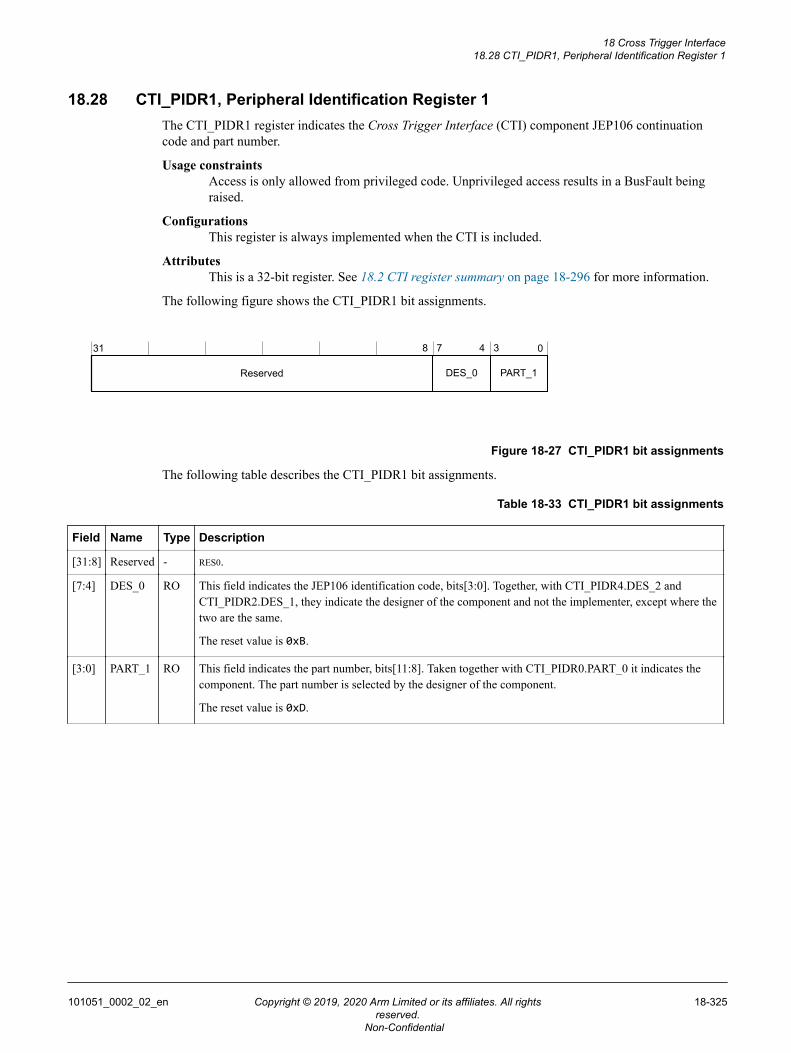
18.28 CTI_PIDR1, Peripheral Identification Register 1The CTI_PIDR1 register indicates the Cross Trigger Interface (CTI) component JEP106 continuationcode and part number.
Usage constraintsAccess is only allowed from privileged code. Unprivileged access results in a BusFault beingraised.
ConfigurationsThis register is always implemented when the CTI is included.
AttributesThis is a 32-bit register. See 18.2 CTI register summary on page 18-296 for more information.
The following figure shows the CTI_PIDR1 bit assignments.
31 8 7 0
Reserved PART_1DES_0
4 3
Figure 18-27 CTI_PIDR1 bit assignments
The following table describes the CTI_PIDR1 bit assignments.
Table 18-33 CTI_PIDR1 bit assignments
Field Name Type Description
[31:8] Reserved - RES0.
[7:4] DES_0 RO This field indicates the JEP106 identification code, bits[3:0]. Together, with CTI_PIDR4.DES_2 andCTI_PIDR2.DES_1, they indicate the designer of the component and not the implementer, except where thetwo are the same.
The reset value is 0xB.
[3:0] PART_1 RO This field indicates the part number, bits[11:8]. Taken together with CTI_PIDR0.PART_0 it indicates thecomponent. The part number is selected by the designer of the component.
The reset value is 0xD.
18 Cross Trigger Interface18.28 CTI_PIDR1, Peripheral Identification Register 1
101051_0002_02_en Copyright © 2019, 2020 Arm Limited or its affiliates. All rightsreserved.
18-325
Non-Confidential
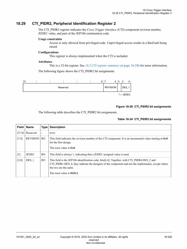
18.29 CTI_PIDR2, Peripheral Identification Register 2The CTI_PIDR2 register indicates the Cross Trigger Interface (CTI) component revision number,JEDEC value, and part of the JEP106 continuation code.
Usage constraintsAccess is only allowed from privileged code. Unprivileged access results in a BusFault beingraised.
ConfigurationsThis register is always implemented when the CTI is included.
AttributesThis is a 32-bit register. See 18.2 CTI register summary on page 18-296 for more information.
The following figure shows the CTI_PIDR2 bit assignments.
31 8 7 0
Reserved DES_1REVISION
4 3 2
JEDEC
Figure 18-28 CTI_PIDR2 bit assignments
The following table describes the CTI_PIDR2 bit assignments.
Table 18-34 CTI_PIDR2 bit assignments
Field Name Type Description
[31:8] Reserved - RES0.
[7:4] REVISION RO This field indicates the revision number of the CTI component. It is an incremental value starting at 0x0for the first design.
The reset value is 0x0.
[3] JEDEC RO This field is always 1, indicating that a JEDEC assigned value is used.
[2:0] DES_1 RO This field is the JEP106 identification code, bits[6:4]. Together, with CTI_PIDR4.DES_2 andCTI_PIDR1.DES_0, they indicate the designer of the component and not the implementer, except wherethe two are the same.
The reset value is 0b011.
18 Cross Trigger Interface18.29 CTI_PIDR2, Peripheral Identification Register 2
101051_0002_02_en Copyright © 2019, 2020 Arm Limited or its affiliates. All rightsreserved.
18-326
Non-Confidential
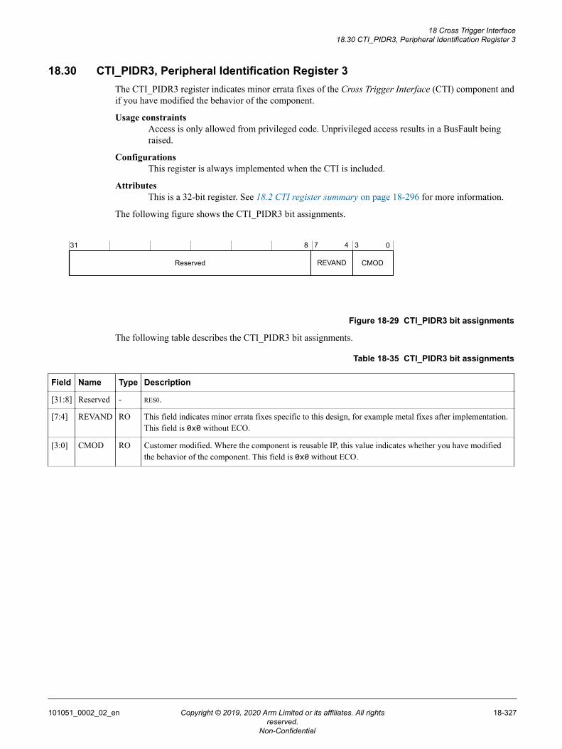
18.30 CTI_PIDR3, Peripheral Identification Register 3The CTI_PIDR3 register indicates minor errata fixes of the Cross Trigger Interface (CTI) component andif you have modified the behavior of the component.
Usage constraintsAccess is only allowed from privileged code. Unprivileged access results in a BusFault beingraised.
ConfigurationsThis register is always implemented when the CTI is included.
AttributesThis is a 32-bit register. See 18.2 CTI register summary on page 18-296 for more information.
The following figure shows the CTI_PIDR3 bit assignments.
31 8 7 0
Reserved CMODREVAND
4 3
Figure 18-29 CTI_PIDR3 bit assignments
The following table describes the CTI_PIDR3 bit assignments.
Table 18-35 CTI_PIDR3 bit assignments
Field Name Type Description
[31:8] Reserved - RES0.
[7:4] REVAND RO This field indicates minor errata fixes specific to this design, for example metal fixes after implementation.This field is 0x0 without ECO.
[3:0] CMOD RO Customer modified. Where the component is reusable IP, this value indicates whether you have modifiedthe behavior of the component. This field is 0x0 without ECO.
18 Cross Trigger Interface18.30 CTI_PIDR3, Peripheral Identification Register 3
101051_0002_02_en Copyright © 2019, 2020 Arm Limited or its affiliates. All rightsreserved.
18-327
Non-Confidential
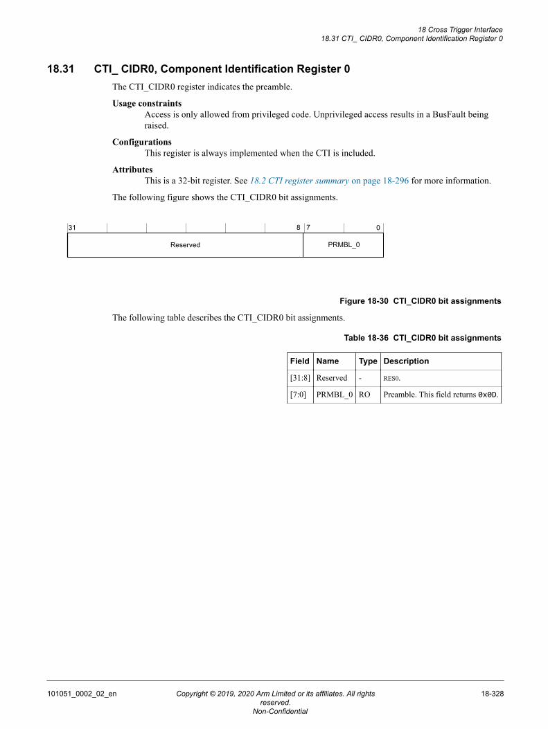
18.31 CTI_ CIDR0, Component Identification Register 0The CTI_CIDR0 register indicates the preamble.
Usage constraintsAccess is only allowed from privileged code. Unprivileged access results in a BusFault beingraised.
ConfigurationsThis register is always implemented when the CTI is included.
AttributesThis is a 32-bit register. See 18.2 CTI register summary on page 18-296 for more information.
The following figure shows the CTI_CIDR0 bit assignments.
31 8 7 0
Reserved PRMBL_0
Figure 18-30 CTI_CIDR0 bit assignments
The following table describes the CTI_CIDR0 bit assignments.
Table 18-36 CTI_CIDR0 bit assignments
Field Name Type Description
[31:8] Reserved - RES0.
[7:0] PRMBL_0 RO Preamble. This field returns 0x0D.
18 Cross Trigger Interface18.31 CTI_ CIDR0, Component Identification Register 0
101051_0002_02_en Copyright © 2019, 2020 Arm Limited or its affiliates. All rightsreserved.
18-328
Non-Confidential
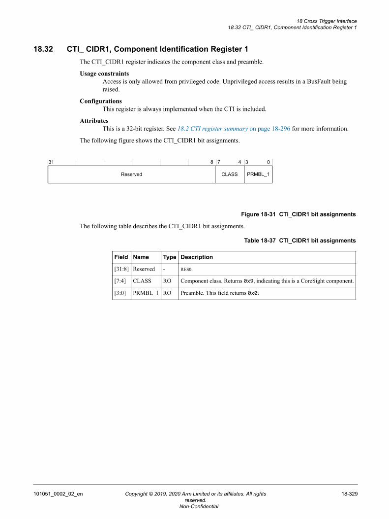
18.32 CTI_ CIDR1, Component Identification Register 1The CTI_CIDR1 register indicates the component class and preamble.
Usage constraintsAccess is only allowed from privileged code. Unprivileged access results in a BusFault beingraised.
ConfigurationsThis register is always implemented when the CTI is included.
AttributesThis is a 32-bit register. See 18.2 CTI register summary on page 18-296 for more information.
The following figure shows the CTI_CIDR1 bit assignments.
31 8 7 0
Reserved PRMBL_1CLASS
4 3
Figure 18-31 CTI_CIDR1 bit assignments
The following table describes the CTI_CIDR1 bit assignments.
Table 18-37 CTI_CIDR1 bit assignments
Field Name Type Description
[31:8] Reserved - RES0.
[7:4] CLASS RO Component class. Returns 0x9, indicating this is a CoreSight component.
[3:0] PRMBL_1 RO Preamble. This field returns 0x0.
18 Cross Trigger Interface18.32 CTI_ CIDR1, Component Identification Register 1
101051_0002_02_en Copyright © 2019, 2020 Arm Limited or its affiliates. All rightsreserved.
18-329
Non-Confidential
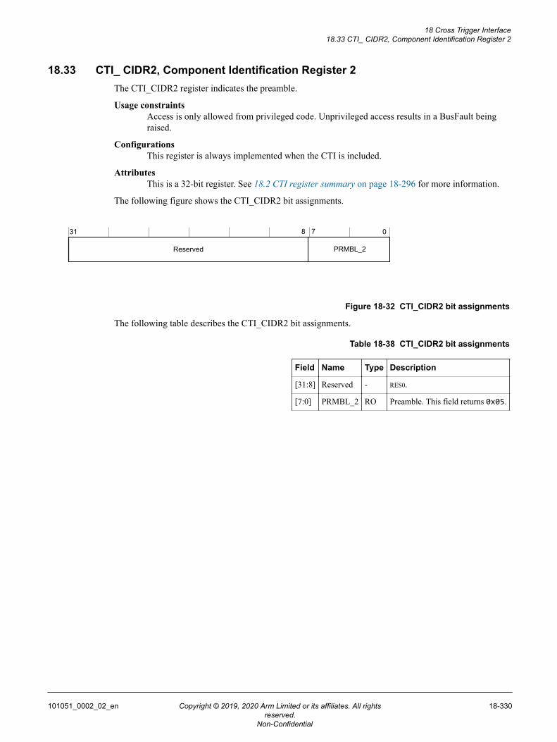
18.33 CTI_ CIDR2, Component Identification Register 2The CTI_CIDR2 register indicates the preamble.
Usage constraintsAccess is only allowed from privileged code. Unprivileged access results in a BusFault beingraised.
ConfigurationsThis register is always implemented when the CTI is included.
AttributesThis is a 32-bit register. See 18.2 CTI register summary on page 18-296 for more information.
The following figure shows the CTI_CIDR2 bit assignments.
31 8 7 0
Reserved PRMBL_2
Figure 18-32 CTI_CIDR2 bit assignments
The following table describes the CTI_CIDR2 bit assignments.
Table 18-38 CTI_CIDR2 bit assignments
Field Name Type Description
[31:8] Reserved - RES0.
[7:0] PRMBL_2 RO Preamble. This field returns 0x05.
18 Cross Trigger Interface18.33 CTI_ CIDR2, Component Identification Register 2
101051_0002_02_en Copyright © 2019, 2020 Arm Limited or its affiliates. All rightsreserved.
18-330
Non-Confidential
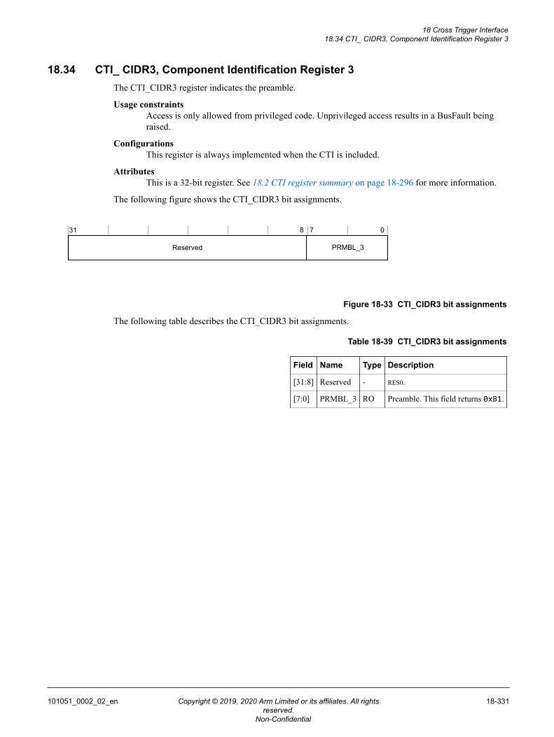
18.34 CTI_ CIDR3, Component Identification Register 3The CTI_CIDR3 register indicates the preamble.
Usage constraintsAccess is only allowed from privileged code. Unprivileged access results in a BusFault beingraised.
ConfigurationsThis register is always implemented when the CTI is included.
AttributesThis is a 32-bit register. See 18.2 CTI register summary on page 18-296 for more information.
The following figure shows the CTI_CIDR3 bit assignments.
31 8 7 0
Reserved PRMBL_3
Figure 18-33 CTI_CIDR3 bit assignments
The following table describes the CTI_CIDR3 bit assignments.
Table 18-39 CTI_CIDR3 bit assignments
Field Name Type Description
[31:8] Reserved - RES0.
[7:0] PRMBL_3 RO Preamble. This field returns 0xB1.
18 Cross Trigger Interface18.34 CTI_ CIDR3, Component Identification Register 3
101051_0002_02_en Copyright © 2019, 2020 Arm Limited or its affiliates. All rightsreserved.
18-331
Non-Confidential
Chapter 19Breakpoint Unit
This chapter describes the Breakpoint Unit (BPU).
It contains the following sections:• 19.1 BPU features on page 19-333.• 19.2 BPU register summary on page 19-334.
101051_0002_02_en Copyright © 2019, 2020 Arm Limited or its affiliates. All rightsreserved.
19-332
Non-Confidential
19.1 BPU featuresThe Breakpoint Unit (BPU) is an implementation of the architectural Flashpoint and Breakpoint (FPB)unit. The BPU can be configured with four or eight instruction address comparators. Each comparatorsupports breakpoint functionality on all instructions that are fetched across the entire address range inwhich code is located.
The BPU does not support flash patching. Flash patching allows a small programmable memory in thesystem to apply patches to program memory that cannot be modified.
The BPU functionality is largely architecturally defined. The IMPLEMENTATION DEFINED functionalityincludes:
SecurityIf the Cortex-M55 processor is configured to include the Security Extension and if invasivedebug is not enabled for the security mode that the processor was in when the breakpointbecame active, then debug events that are associated with breakpoints are blocked.
Architectural remap registersThe Cortex-M55 processor does not include the address remapping functionality for instructionsand literals. Therefore, the following architecturally defined registers have the followingbehavior:• FP_REMAP.RMPSPT is RAZ/WI.• FP_REMAP.REMAP is Reserved.• FP_CTRL.NUM_LIT is 0, indicating that no literal comparators are included.• Attempting to enable Flash Patch in FP_COMPn is ignored.
Additionally, only instruction address comparators are supported.
For more information on the registers listed in this section, see the Arm®v8-M Architecture ReferenceManual.
19 Breakpoint Unit19.1 BPU features
101051_0002_02_en Copyright © 2019, 2020 Arm Limited or its affiliates. All rightsreserved.
19-333
Non-Confidential
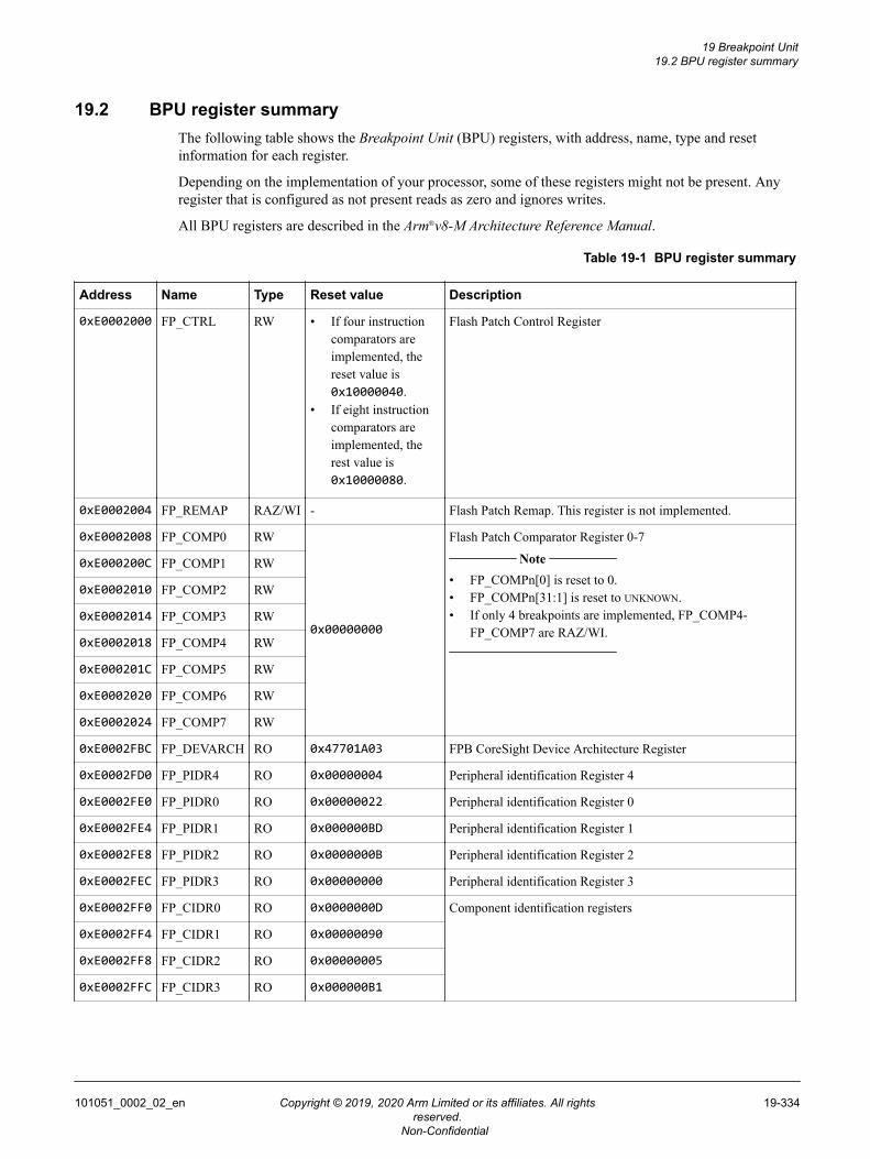
19.2 BPU register summaryThe following table shows the Breakpoint Unit (BPU) registers, with address, name, type and resetinformation for each register.
Depending on the implementation of your processor, some of these registers might not be present. Anyregister that is configured as not present reads as zero and ignores writes.
All BPU registers are described in the Arm®v8-M Architecture Reference Manual.
Table 19-1 BPU register summary
Address Name Type Reset value Description
0xE0002000 FP_CTRL RW • If four instructioncomparators areimplemented, thereset value is0x10000040.
• If eight instructioncomparators areimplemented, therest value is0x10000080.
Flash Patch Control Register
0xE0002004 FP_REMAP RAZ/WI - Flash Patch Remap. This register is not implemented.
0xE0002008 FP_COMP0 RW
0x00000000
Flash Patch Comparator Register 0-7 Note
• FP_COMPn[0] is reset to 0.• FP_COMPn[31:1] is reset to UNKNOWN.• If only 4 breakpoints are implemented, FP_COMP4-
FP_COMP7 are RAZ/WI.
0xE000200C FP_COMP1 RW
0xE0002010 FP_COMP2 RW
0xE0002014 FP_COMP3 RW
0xE0002018 FP_COMP4 RW
0xE000201C FP_COMP5 RW
0xE0002020 FP_COMP6 RW
0xE0002024 FP_COMP7 RW
0xE0002FBC FP_DEVARCH RO 0x47701A03 FPB CoreSight Device Architecture Register
0xE0002FD0 FP_PIDR4 RO 0x00000004 Peripheral identification Register 4
0xE0002FE0 FP_PIDR0 RO 0x00000022 Peripheral identification Register 0
0xE0002FE4 FP_PIDR1 RO 0x000000BD Peripheral identification Register 1
0xE0002FE8 FP_PIDR2 RO 0x0000000B Peripheral identification Register 2
0xE0002FEC FP_PIDR3 RO 0x00000000 Peripheral identification Register 3
0xE0002FF0 FP_CIDR0 RO 0x0000000D Component identification registers
0xE0002FF4 FP_CIDR1 RO 0x00000090
0xE0002FF8 FP_CIDR2 RO 0x00000005
0xE0002FFC FP_CIDR3 RO 0x000000B1
19 Breakpoint Unit19.2 BPU register summary
101051_0002_02_en Copyright © 2019, 2020 Arm Limited or its affiliates. All rightsreserved.
19-334
Non-Confidential

Note
FP_DEVTYPE, FP_PIDR5, FP_PIDR6, and FP_PIDR7 registers are not implemented, and are RES0.
19 Breakpoint Unit19.2 BPU register summary
101051_0002_02_en Copyright © 2019, 2020 Arm Limited or its affiliates. All rightsreserved.
19-335
Non-Confidential
Appendix AExternal Wakeup Interrupt Controller
This appendix describes the External Wakeup Interrupt Controller (EWIC) that can be used with theCortex-M55 processor.
It contains the following sections:• A.1 EWIC features on page Appx-A-337.• A.2 EWIC register summary on page Appx-A-338.
101051_0002_02_en Copyright © 2019, 2020 Arm Limited or its affiliates. All rightsreserved.
Appx-A-336
Non-Confidential
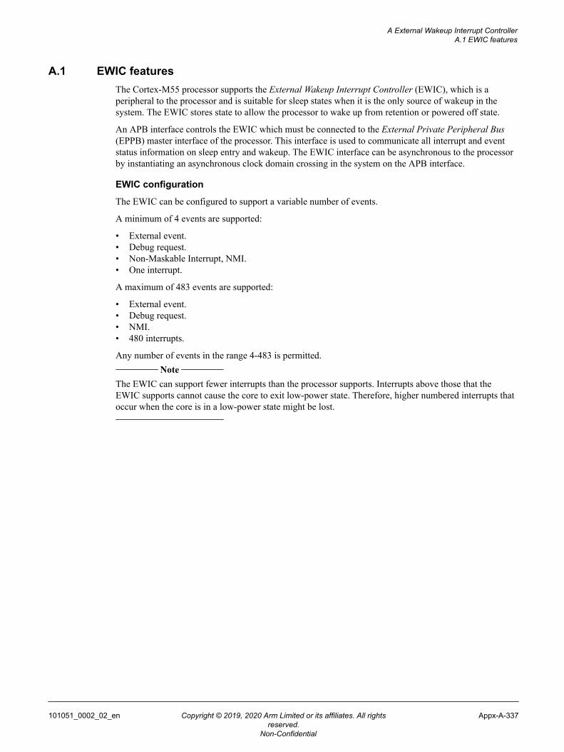
A.1 EWIC featuresThe Cortex-M55 processor supports the External Wakeup Interrupt Controller (EWIC), which is aperipheral to the processor and is suitable for sleep states when it is the only source of wakeup in thesystem. The EWIC stores state to allow the processor to wake up from retention or powered off state.
An APB interface controls the EWIC which must be connected to the External Private Peripheral Bus(EPPB) master interface of the processor. This interface is used to communicate all interrupt and eventstatus information on sleep entry and wakeup. The EWIC interface can be asynchronous to the processorby instantiating an asynchronous clock domain crossing in the system on the APB interface.
EWIC configuration
The EWIC can be configured to support a variable number of events.
A minimum of 4 events are supported:
• External event.• Debug request.• Non-Maskable Interrupt, NMI.• One interrupt.
A maximum of 483 events are supported:
• External event.• Debug request.• NMI.• 480 interrupts.
Any number of events in the range 4-483 is permitted. Note
The EWIC can support fewer interrupts than the processor supports. Interrupts above those that theEWIC supports cannot cause the core to exit low-power state. Therefore, higher numbered interrupts thatoccur when the core is in a low-power state might be lost.
A External Wakeup Interrupt ControllerA.1 EWIC features
101051_0002_02_en Copyright © 2019, 2020 Arm Limited or its affiliates. All rightsreserved.
Appx-A-337
Non-Confidential
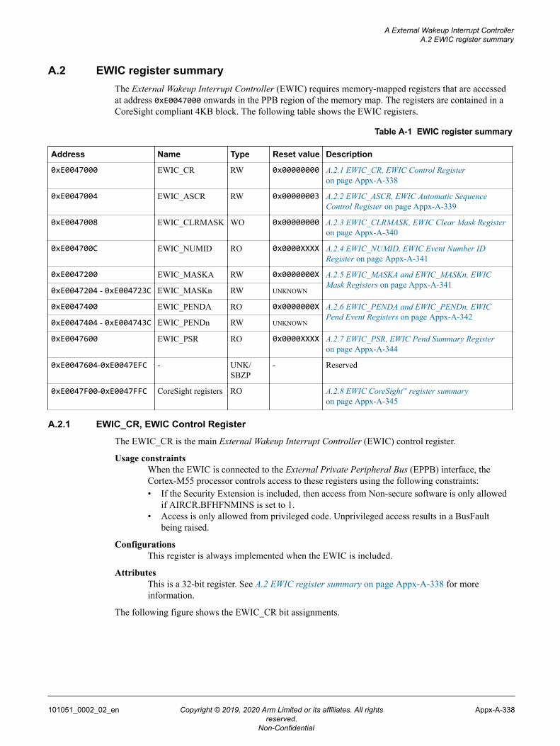
A.2 EWIC register summaryThe External Wakeup Interrupt Controller (EWIC) requires memory-mapped registers that are accessedat address 0xE0047000 onwards in the PPB region of the memory map. The registers are contained in aCoreSight compliant 4KB block. The following table shows the EWIC registers.
Table A-1 EWIC register summary
Address Name Type Reset value Description
0xE0047000 EWIC_CR RW 0x00000000 A.2.1 EWIC_CR, EWIC Control Registeron page Appx-A-338
0xE0047004 EWIC_ASCR RW 0x00000003 A.2.2 EWIC_ASCR, EWIC Automatic SequenceControl Register on page Appx-A-339
0xE0047008 EWIC_CLRMASK WO 0x00000000 A.2.3 EWIC_CLRMASK, EWIC Clear Mask Registeron page Appx-A-340
0xE004700C EWIC_NUMID RO 0x0000XXXX A.2.4 EWIC_NUMID, EWIC Event Number IDRegister on page Appx-A-341
0xE0047200 EWIC_MASKA RW 0x0000000X A.2.5 EWIC_MASKA and EWIC_MASKn, EWICMask Registers on page Appx-A-341
0xE0047204 - 0xE004723C EWIC_MASKn RW UNKNOWN
0xE0047400 EWIC_PENDA RO 0x0000000X A.2.6 EWIC_PENDA and EWIC_PENDn, EWICPend Event Registers on page Appx-A-342
0xE0047404 - 0xE004743C EWIC_PENDn RW UNKNOWN
0xE0047600 EWIC_PSR RO 0x0000XXXX A.2.7 EWIC_PSR, EWIC Pend Summary Registeron page Appx-A-344
0xE0047604-0xE0047EFC - UNK/SBZP
- Reserved
0xE0047F00-0xE0047FFC CoreSight registers RO A.2.8 EWIC CoreSight™ register summaryon page Appx-A-345
A.2.1 EWIC_CR, EWIC Control Register
The EWIC_CR is the main External Wakeup Interrupt Controller (EWIC) control register.
Usage constraintsWhen the EWIC is connected to the External Private Peripheral Bus (EPPB) interface, theCortex-M55 processor controls access to these registers using the following constraints:• If the Security Extension is included, then access from Non-secure software is only allowed
if AIRCR.BFHFNMINS is set to 1.• Access is only allowed from privileged code. Unprivileged access results in a BusFault
being raised.
ConfigurationsThis register is always implemented when the EWIC is included.
AttributesThis is a 32-bit register. See A.2 EWIC register summary on page Appx-A-338 for moreinformation.
The following figure shows the EWIC_CR bit assignments.
A External Wakeup Interrupt ControllerA.2 EWIC register summary
101051_0002_02_en Copyright © 2019, 2020 Arm Limited or its affiliates. All rightsreserved.
Appx-A-338
Non-Confidential
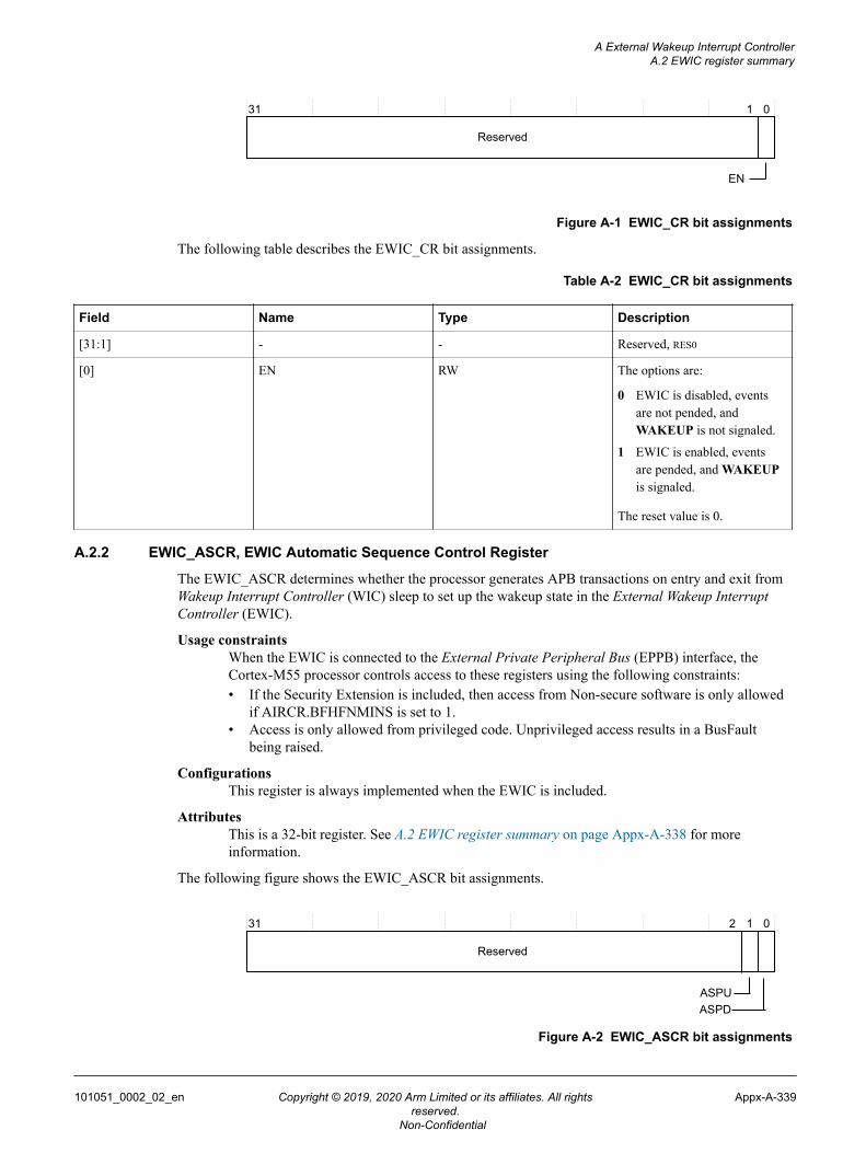
31 01
EN
Reserved
Figure A-1 EWIC_CR bit assignments
The following table describes the EWIC_CR bit assignments.
Table A-2 EWIC_CR bit assignments
Field Name Type Description
[31:1] - - Reserved, RES0
[0] EN RW The options are:
0 EWIC is disabled, eventsare not pended, andWAKEUP is not signaled.
1 EWIC is enabled, eventsare pended, and WAKEUPis signaled.
The reset value is 0.
A.2.2 EWIC_ASCR, EWIC Automatic Sequence Control Register
The EWIC_ASCR determines whether the processor generates APB transactions on entry and exit fromWakeup Interrupt Controller (WIC) sleep to set up the wakeup state in the External Wakeup InterruptController (EWIC).
Usage constraintsWhen the EWIC is connected to the External Private Peripheral Bus (EPPB) interface, theCortex-M55 processor controls access to these registers using the following constraints:• If the Security Extension is included, then access from Non-secure software is only allowed
if AIRCR.BFHFNMINS is set to 1.• Access is only allowed from privileged code. Unprivileged access results in a BusFault
being raised.
ConfigurationsThis register is always implemented when the EWIC is included.
AttributesThis is a 32-bit register. See A.2 EWIC register summary on page Appx-A-338 for moreinformation.
The following figure shows the EWIC_ASCR bit assignments.
31 01
ASPU
Reserved
2
ASPD
Figure A-2 EWIC_ASCR bit assignments
A External Wakeup Interrupt ControllerA.2 EWIC register summary
101051_0002_02_en Copyright © 2019, 2020 Arm Limited or its affiliates. All rightsreserved.
Appx-A-339
Non-Confidential
The following table describes the EWIC_ASCR bit assignments.
Table A-3 EWIC_ASCR bit assignments
Field Name Type Description
[31:2] - - Reserved, RES0
[1] ASPU RW The value of this bit is sent tothe processor. The processormust use this value to decidewhether any automatic EWICaccesses must be performed ontransitioning from a low-powerstate. The options are:
0 No automatic sequence onpowerup.
1 Automatic sequence onpowerup.
The reset value is 1.
[0] ASPD RW The value of this bit is sent tothe processor. The processormust use this value to decidewhether any automatic EWICaccesses must be performed ontransitioning to a low-powerstate. The options are:
0 No automatic sequence onentry to a low-power state.
1 Automatic sequence onentry to a low-power state.
The reset value is 1.
Note
• If the automatic sequence is disabled, then software can program the unit by writing to theEWIC_MASKA and EWIC_MASKn registers on sleep entry and reading from the EWIC_PENDnregisters on sleep exit. For more information, see A.2.5 EWIC_MASKA and EWIC_MASKn, EWICMask Registers on page Appx-A-341 and A.2.6 EWIC_PENDA and EWIC_PENDn, EWIC PendEvent Registers on page Appx-A-342.
• The value of EWIC_ASCR does not affect the operation of the EWIC itself. It only affects the controlinformation that is driven on the WICCONTROL signal to the Cortex-M55 processor.
• When modifying EWIC_ASCR.ASPU and EWIC_ACSR.ASPD, the resulting changes toWICCONTROL[3:0] must be stable before software enters sleep and remain stable until softwareexecution resumes. Otherwise, modification of these registers can result in UNPREDICTABLE behavior.
A.2.3 EWIC_CLRMASK, EWIC Clear Mask Register
When there is a write to the EWIC_CLRMASK register, it causes EWIC_MASKA and all theEWIC_MASKn registers to be cleared. The write data is ignored. This register is RAZ.
A External Wakeup Interrupt ControllerA.2 EWIC register summary
101051_0002_02_en Copyright © 2019, 2020 Arm Limited or its affiliates. All rightsreserved.
Appx-A-340
Non-Confidential
A.2.4 EWIC_NUMID, EWIC Event Number ID Register
The EWIC_NUMID register returns the total number of events that are supported in the External WakeupInterrupt Controller (EWIC).
Usage constraintsWhen the EWIC is connected to the External Private Peripheral Bus (EPPB) interface, theCortex-M55 processor controls access to these registers using the following constraints:• If the Security Extension is included, then access from Non-secure software is only allowed
if AIRCR.BFHFNMINS is set to 1.• Access is only allowed from privileged code. Unprivileged access results in a BusFault
being raised.
ConfigurationsThis register is always implemented when the EWIC is included.
AttributesThis is a 32-bit register. See A.2 EWIC register summary on page Appx-A-338 for moreinformation.
The following figure shows the EWIC_NUMID bit assignments.
31 16 15 0
NUMEVENTReserved
Figure A-3 EWIC_NUMID bit assignments
The following table describes the EWIC_NUMID bit assignments.
Table A-4 EWIC_NUMID bit assignments
Field Name Type Description
[31:16] - - Reserved, RES0
[15:0] NUMEVENT RO The number of eventssupported.
A.2.5 EWIC_MASKA and EWIC_MASKn, EWIC Mask Registers
The EWIC_MASKA register defines the mask for special events and the EWIC_MASKn registers forexternal interrupt (IRQ) events. There is one EWIC_MASKn register implemented for every 32 externalinterrupts that the External Wakeup Interrupt Controller (EWIC) supports. At least one register is alwaysimplemented. EWIC_MASKn is at address 0xE0047204+(n×4), where n=0-14.
Usage constraintsWhen the EWIC is connected to the External Private Peripheral Bus (EPPB) interface, theCortex-M55 processor controls access to these registers using the following constraints:• If the Security Extension is included, then access from Non-secure software is only allowed
if AIRCR.BFHFNMINS is set to 1.• Access is only allowed from privileged code. Unprivileged access results in a BusFault
being raised.
ConfigurationsThese registers are always implemented when the EWIC is included.
AttributesThese are 32-bit registers. See A.2 EWIC register summary on page Appx-A-338 for moreinformation.
A External Wakeup Interrupt ControllerA.2 EWIC register summary
101051_0002_02_en Copyright © 2019, 2020 Arm Limited or its affiliates. All rightsreserved.
Appx-A-341
Non-Confidential
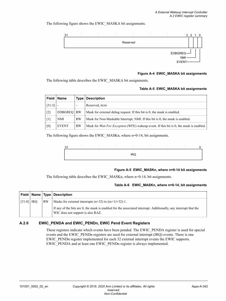
The following figure shows the EWIC_MASKA bit assignments.
31 01
EDBGREQ
Reserved
23
NMIEVENT
Figure A-4 EWIC_MASKA bit assignments
The following table describes the EWIC_MASKA bit assignments.
Table A-5 EWIC_MASKA bit assignments
Field Name Type Description
[31:3] - - Reserved, RES0
[2] EDBGREQ RW Mask for external debug request. If this bit is 0, the mask is enabled.
[1] NMI RW Mask for Non-Maskable Interrupt, NMI. If this bit is 0, the mask is enabled.
[0] EVENT RW Mask for Wait For Exception (WFE) wakeup event. If this bit is 0, the mask is enabled.
The following figure shows the EWIC_MASKn, where n=0-14, bit assignments.
31 0
IRQ
Figure A-5 EWIC_MASKn, where n=0-14 bit assignments
The following table describes the EWIC_MASKn, where n=0-14, bit assignments.
Table A-6 EWIC_MASKn, where n=0-14, bit assignments
Field Name Type Description
[31:0] IRQ RW Masks for external interrupts (n×32) to ((n+1)×32)-1.
If any of the bits are 0, the mask is enabled for the associated interrupt. Additionally, any interrupt that theWIC does not support is also RAZ.
A.2.6 EWIC_PENDA and EWIC_PENDn, EWIC Pend Event Registers
These registers indicate which events have been pended. The EWIC_PENDA register is used for specialevents and the EWIC_PENDn registers are used for external interrupt (IRQ) events. There is oneEWIC_PENDn register implemented for each 32 external interrupt events the EWIC supports.EWIC_PENDA and at least one EWIC_PENDn register is always implemented.
A External Wakeup Interrupt ControllerA.2 EWIC register summary
101051_0002_02_en Copyright © 2019, 2020 Arm Limited or its affiliates. All rightsreserved.
Appx-A-342
Non-Confidential
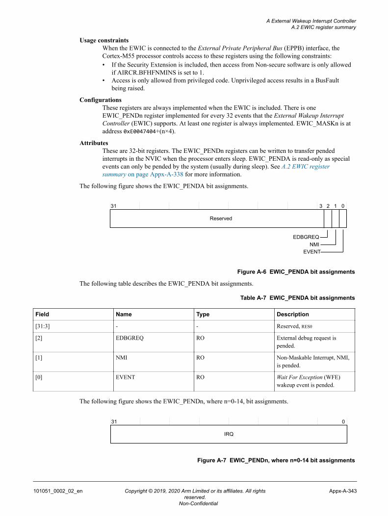
Usage constraintsWhen the EWIC is connected to the External Private Peripheral Bus (EPPB) interface, theCortex-M55 processor controls access to these registers using the following constraints:• If the Security Extension is included, then access from Non-secure software is only allowed
if AIRCR.BFHFNMINS is set to 1.• Access is only allowed from privileged code. Unprivileged access results in a BusFault
being raised.
ConfigurationsThese registers are always implemented when the EWIC is included. There is oneEWIC_PENDn register implemented for every 32 events that the External Wakeup InterruptController (EWIC) supports. At least one register is always implemented. EWIC_MASKn is ataddress 0xE0047404+(n×4).
AttributesThese are 32-bit registers. The EWIC_PENDn registers can be written to transfer pendedinterrupts in the NVIC when the processor enters sleep. EWIC_PENDA is read-only as specialevents can only be pended by the system (usually during sleep). See A.2 EWIC registersummary on page Appx-A-338 for more information.
The following figure shows the EWIC_PENDA bit assignments.
31 01
EDBGREQ
Reserved
23
NMIEVENT
Figure A-6 EWIC_PENDA bit assignments
The following table describes the EWIC_PENDA bit assignments.
Table A-7 EWIC_PENDA bit assignments
Field Name Type Description
[31:3] - - Reserved, RES0
[2] EDBGREQ RO External debug request ispended.
[1] NMI RO Non-Maskable Interrupt, NMI,is pended.
[0] EVENT RO Wait For Exception (WFE)wakeup event is pended.
The following figure shows the EWIC_PENDn, where n=0-14, bit assignments.
31 0
IRQ
Figure A-7 EWIC_PENDn, where n=0-14 bit assignments
A External Wakeup Interrupt ControllerA.2 EWIC register summary
101051_0002_02_en Copyright © 2019, 2020 Arm Limited or its affiliates. All rightsreserved.
Appx-A-343
Non-Confidential
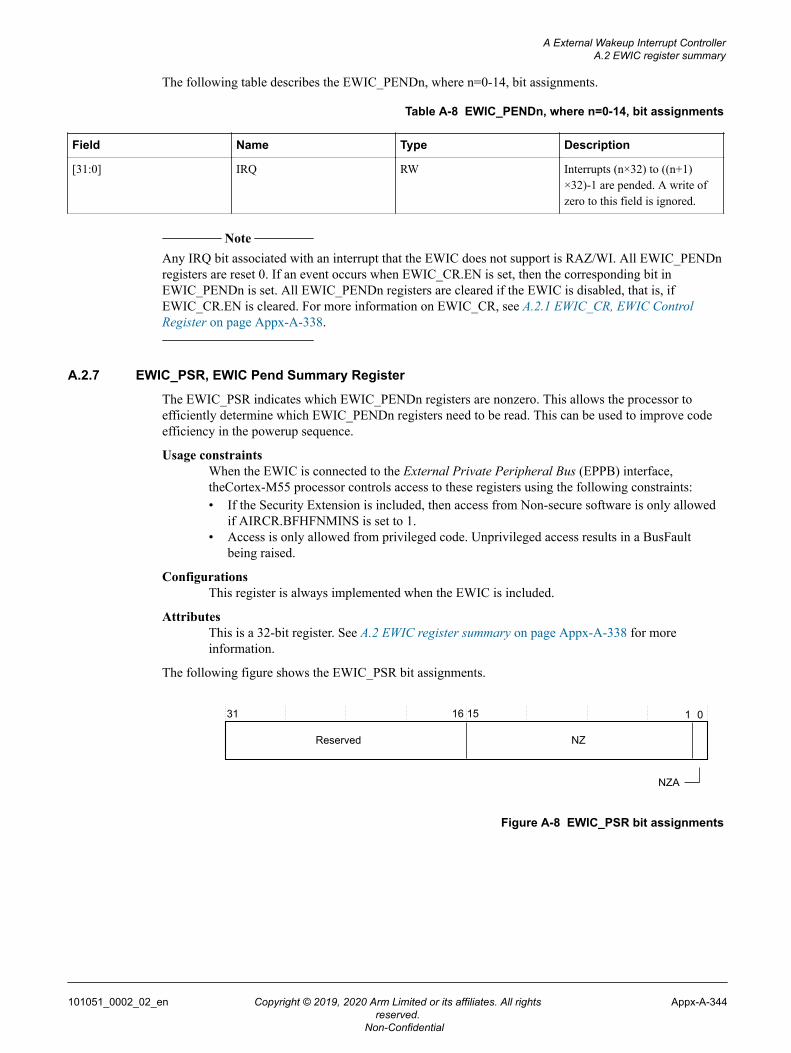
The following table describes the EWIC_PENDn, where n=0-14, bit assignments.
Table A-8 EWIC_PENDn, where n=0-14, bit assignments
Field Name Type Description
[31:0] IRQ RW Interrupts (n×32) to ((n+1)×32)-1 are pended. A write ofzero to this field is ignored.
Note
Any IRQ bit associated with an interrupt that the EWIC does not support is RAZ/WI. All EWIC_PENDnregisters are reset 0. If an event occurs when EWIC_CR.EN is set, then the corresponding bit inEWIC_PENDn is set. All EWIC_PENDn registers are cleared if the EWIC is disabled, that is, ifEWIC_CR.EN is cleared. For more information on EWIC_CR, see A.2.1 EWIC_CR, EWIC ControlRegister on page Appx-A-338.
A.2.7 EWIC_PSR, EWIC Pend Summary Register
The EWIC_PSR indicates which EWIC_PENDn registers are nonzero. This allows the processor toefficiently determine which EWIC_PENDn registers need to be read. This can be used to improve codeefficiency in the powerup sequence.
Usage constraintsWhen the EWIC is connected to the External Private Peripheral Bus (EPPB) interface,theCortex-M55 processor controls access to these registers using the following constraints:• If the Security Extension is included, then access from Non-secure software is only allowed
if AIRCR.BFHFNMINS is set to 1.• Access is only allowed from privileged code. Unprivileged access results in a BusFault
being raised.
ConfigurationsThis register is always implemented when the EWIC is included.
AttributesThis is a 32-bit register. See A.2 EWIC register summary on page Appx-A-338 for moreinformation.
The following figure shows the EWIC_PSR bit assignments.
31 0
Reserved
16 15
NZ
1
NZA
Figure A-8 EWIC_PSR bit assignments
A External Wakeup Interrupt ControllerA.2 EWIC register summary
101051_0002_02_en Copyright © 2019, 2020 Arm Limited or its affiliates. All rightsreserved.
Appx-A-344
Non-Confidential
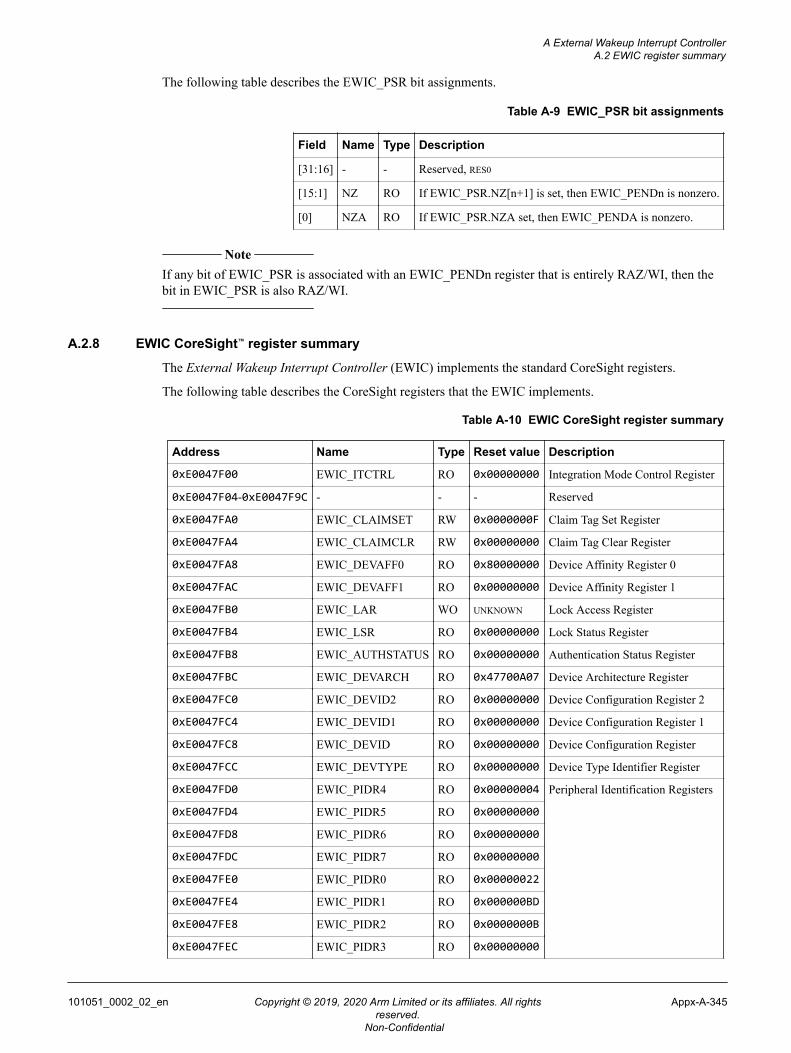
The following table describes the EWIC_PSR bit assignments.
Table A-9 EWIC_PSR bit assignments
Field Name Type Description
[31:16] - - Reserved, RES0
[15:1] NZ RO If EWIC_PSR.NZ[n+1] is set, then EWIC_PENDn is nonzero.
[0] NZA RO If EWIC_PSR.NZA set, then EWIC_PENDA is nonzero.
Note
If any bit of EWIC_PSR is associated with an EWIC_PENDn register that is entirely RAZ/WI, then thebit in EWIC_PSR is also RAZ/WI.
A.2.8 EWIC CoreSight™ register summary
The External Wakeup Interrupt Controller (EWIC) implements the standard CoreSight registers.
The following table describes the CoreSight registers that the EWIC implements.
Table A-10 EWIC CoreSight register summary
Address Name Type Reset value Description
0xE0047F00 EWIC_ITCTRL RO 0x00000000 Integration Mode Control Register
0xE0047F04-0xE0047F9C - - - Reserved
0xE0047FA0 EWIC_CLAIMSET RW 0x0000000F Claim Tag Set Register
0xE0047FA4 EWIC_CLAIMCLR RW 0x00000000 Claim Tag Clear Register
0xE0047FA8 EWIC_DEVAFF0 RO 0x80000000 Device Affinity Register 0
0xE0047FAC EWIC_DEVAFF1 RO 0x00000000 Device Affinity Register 1
0xE0047FB0 EWIC_LAR WO UNKNOWN Lock Access Register
0xE0047FB4 EWIC_LSR RO 0x00000000 Lock Status Register
0xE0047FB8 EWIC_AUTHSTATUS RO 0x00000000 Authentication Status Register
0xE0047FBC EWIC_DEVARCH RO 0x47700A07 Device Architecture Register
0xE0047FC0 EWIC_DEVID2 RO 0x00000000 Device Configuration Register 2
0xE0047FC4 EWIC_DEVID1 RO 0x00000000 Device Configuration Register 1
0xE0047FC8 EWIC_DEVID RO 0x00000000 Device Configuration Register
0xE0047FCC EWIC_DEVTYPE RO 0x00000000 Device Type Identifier Register
0xE0047FD0 EWIC_PIDR4 RO 0x00000004 Peripheral Identification Registers
0xE0047FD4 EWIC_PIDR5 RO 0x00000000
0xE0047FD8 EWIC_PIDR6 RO 0x00000000
0xE0047FDC EWIC_PIDR7 RO 0x00000000
0xE0047FE0 EWIC_PIDR0 RO 0x00000022
0xE0047FE4 EWIC_PIDR1 RO 0x000000BD
0xE0047FE8 EWIC_PIDR2 RO 0x0000000B
0xE0047FEC EWIC_PIDR3 RO 0x00000000
A External Wakeup Interrupt ControllerA.2 EWIC register summary
101051_0002_02_en Copyright © 2019, 2020 Arm Limited or its affiliates. All rightsreserved.
Appx-A-345
Non-Confidential
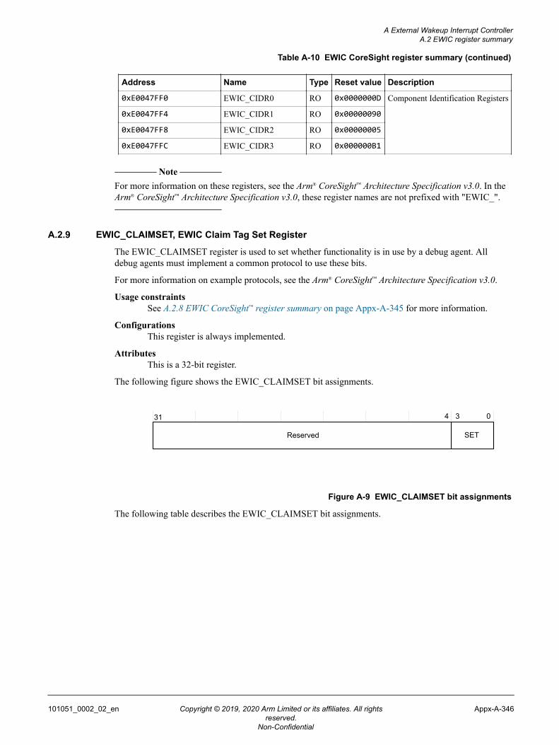
Table A-10 EWIC CoreSight register summary (continued)
Address Name Type Reset value Description
0xE0047FF0 EWIC_CIDR0 RO 0x0000000D Component Identification Registers
0xE0047FF4 EWIC_CIDR1 RO 0x00000090
0xE0047FF8 EWIC_CIDR2 RO 0x00000005
0xE0047FFC EWIC_CIDR3 RO 0x000000B1
Note
For more information on these registers, see the Arm® CoreSight™ Architecture Specification v3.0. In theArm® CoreSight™ Architecture Specification v3.0, these register names are not prefixed with "EWIC_".
A.2.9 EWIC_CLAIMSET, EWIC Claim Tag Set Register
The EWIC_CLAIMSET register is used to set whether functionality is in use by a debug agent. Alldebug agents must implement a common protocol to use these bits.
For more information on example protocols, see the Arm® CoreSight™ Architecture Specification v3.0.
Usage constraintsSee A.2.8 EWIC CoreSight™ register summary on page Appx-A-345 for more information.
ConfigurationsThis register is always implemented.
AttributesThis is a 32-bit register.
The following figure shows the EWIC_CLAIMSET bit assignments.
31 34
SETReserved
0
Figure A-9 EWIC_CLAIMSET bit assignments
The following table describes the EWIC_CLAIMSET bit assignments.
A External Wakeup Interrupt ControllerA.2 EWIC register summary
101051_0002_02_en Copyright © 2019, 2020 Arm Limited or its affiliates. All rightsreserved.
Appx-A-346
Non-Confidential
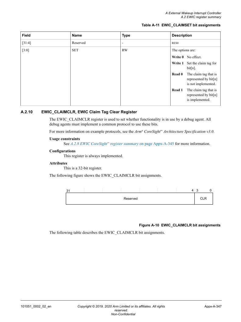
Table A-11 EWIC_CLAIMSET bit assignments
Field Name Type Description
[31:4] Reserved - RES0
[3:0] SET RW The options are:
Write 0 No effect.
Write 1 Set the claim tag forbit[n].
Read 0 The claim tag that isrepresented by bit[n]is not implemented.
Read 1 The claim tag that isrepresented by bit[n]is implemented.
A.2.10 EWIC_CLAIMCLR, EWIC Claim Tag Clear Register
The EWIC_CLAIMCLR register is used to set whether functionality is in use by a debug agent. Alldebug agents must implement a common protocol to use these bits.
For more information on example protocols, see the Arm® CoreSight™ Architecture Specification v3.0.
Usage constraintsSee A.2.8 EWIC CoreSight™ register summary on page Appx-A-345 for more information.
ConfigurationsThis register is always implemented.
AttributesThis is a 32-bit register.
The following figure shows the EWIC_CLAIMCLR bit assignments.
31 34
CLRReserved
0
Figure A-10 EWIC_CLAIMCLR bit assignments
The following table describes the EWIC_CLAIMCLR bit assignments.
A External Wakeup Interrupt ControllerA.2 EWIC register summary
101051_0002_02_en Copyright © 2019, 2020 Arm Limited or its affiliates. All rightsreserved.
Appx-A-347
Non-Confidential
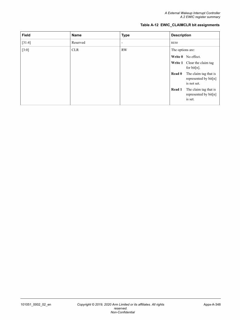
Table A-12 EWIC_CLAIMCLR bit assignments
Field Name Type Description
[31:4] Reserved - RES0
[3:0] CLR RW The options are:
Write 0 No effect.
Write 1 Clear the claim tagfor bit[n].
Read 0 The claim tag that isrepresented by bit[n]is not set.
Read 1 The claim tag that isrepresented by bit[n]is set.
A External Wakeup Interrupt ControllerA.2 EWIC register summary
101051_0002_02_en Copyright © 2019, 2020 Arm Limited or its affiliates. All rightsreserved.
Appx-A-348
Non-Confidential
Appendix BTrace Port Interface Unit
This appendix describes the Trace Port Interface Unit (TPIU) that can be used with the Cortex-M55processor.
It contains the following sections:• B.1 TPIU features on page Appx-B-350.• B.2 TPIU register summary on page Appx-B-353.
101051_0002_02_en Copyright © 2019, 2020 Arm Limited or its affiliates. All rightsreserved.
Appx-B-349
Non-Confidential
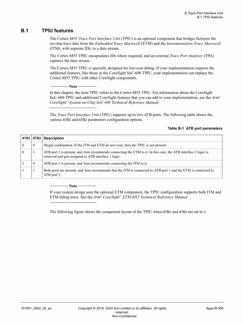
B.1 TPIU featuresThe Cortex-M55 Trace Port Interface Unit (TPIU) is an optional component that bridges between theon-chip trace data from the Embedded Trace Macrocell (ETM) and the Instrumentation Trace Macrocell(ITM), with separate IDs, to a data stream.
The Cortex-M55 TPIU encapsulates IDs where required, and an external Trace Port Analyzer (TPA)captures the data stream.
The Cortex-M55 TPIU is specially designed for low-cost debug. If your implementation requires theadditional features, like those in the CoreSight SoC-600 TPIU, your implementation can replace theCortex-M55 TPIU with other CoreSight components.
Note
In this chapter, the term TPIU refers to the Cortex-M55 TPIU. For information about the CoreSightSoC-600 TPIU and additional CoreSight features that you can add to your implementation, see the Arm®
CoreSight™ System-on-Chip SoC-600 Technical Reference Manual.
The Trace Port Interface Unit (TPIU) supports up to two ATB ports. The following table shows thevarious ATB1 and ATB2 parameters configuration options.
Table B-1 ATB port parameters
ATB1 ATB2 Description
0 0 Illegal combination. If the ITM and ETM do not exist, then the TPIU is not present.
0 1 ATB port 2 is present, and Arm recommends connecting the ETM to it. In this case, the ATB interface 2 logic isremoved and gets assigned to ATB interface 1 logic.
1 0 ATB port 1 is present, and Arm recommends connecting the ITM to it.
1 1 Both ports are present, and Arm recommends that the ITM is connected to ATB port 1 and the ETM is connected toATB port 2.
Note
If your system design uses the optional ETM component, the TPIU configuration supports both ITM andETM debug trace. See the Arm® CoreSight™ ETM‑M55 Technical Reference Manual.
The following figure shows the component layout of the TPIU when ATB1 and ATB2 are set to 1.
B Trace Port Interface UnitB.1 TPIU features
101051_0002_02_en Copyright © 2019, 2020 Arm Limited or its affiliates. All rightsreserved.
Appx-B-350
Non-Confidential
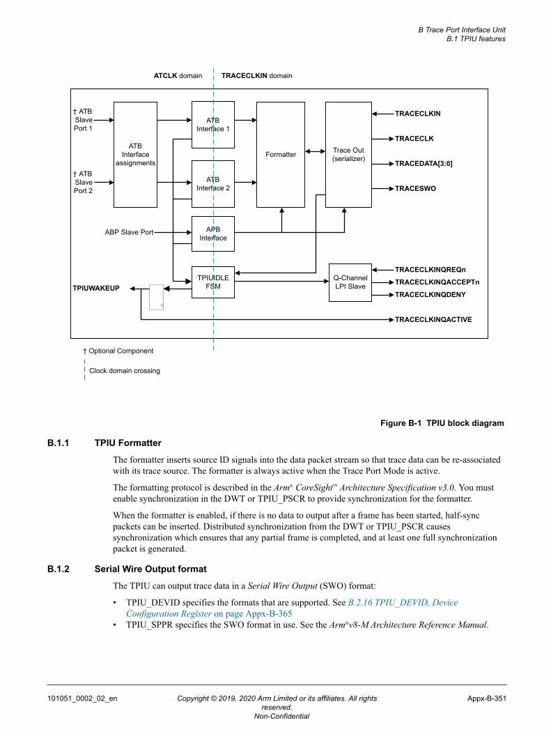
ATBInterface
assignments
ATBInterface 1
ATBInterface 2
Formatter Trace Out(serializer)
APBInterface
† ATBSlavePort 1
† ATBSlavePort 2
TRACECLKIN
TRACECLK
TRACEDATA[3:0]
TRACESWO
ABP Slave Port
† Optional Component
TPIUIDLEFSM
Q-ChannelLPI SlaveTPIUWAKEUP
TRACECLKINQREQn
TRACECLKINQACCEPTn
TRACECLKINQDENY
TRACECLKINQACTIVE
ATCLK domain TRACECLKIN domain
Clock domain crossing
Figure B-1 TPIU block diagram
B.1.1 TPIU Formatter
The formatter inserts source ID signals into the data packet stream so that trace data can be re-associatedwith its trace source. The formatter is always active when the Trace Port Mode is active.
The formatting protocol is described in the Arm® CoreSight™ Architecture Specification v3.0. You mustenable synchronization in the DWT or TPIU_PSCR to provide synchronization for the formatter.
When the formatter is enabled, if there is no data to output after a frame has been started, half-syncpackets can be inserted. Distributed synchronization from the DWT or TPIU_PSCR causessynchronization which ensures that any partial frame is completed, and at least one full synchronizationpacket is generated.
B.1.2 Serial Wire Output format
The TPIU can output trace data in a Serial Wire Output (SWO) format:
• TPIU_DEVID specifies the formats that are supported. See B.2.16 TPIU_DEVID, DeviceConfiguration Register on page Appx-B-365
• TPIU_SPPR specifies the SWO format in use. See the Arm®v8-M Architecture Reference Manual.
B Trace Port Interface UnitB.1 TPIU features
101051_0002_02_en Copyright © 2019, 2020 Arm Limited or its affiliates. All rightsreserved.
Appx-B-351
Non-Confidential
When one of the two SWO modes is selected, you can enable the TPIU to bypass the formatter for traceoutput. When the formatter is bypassed, only data on the ATB interface 1 is passed through and ATBinterface 2 data is discarded.
Note
When operating in bypass mode, Arm recommends that in a configuration that supports an ETM andITM, the ITM data is passed through by connecting the ITM to the ATB Slave Port 1.
B Trace Port Interface UnitB.1 TPIU features
101051_0002_02_en Copyright © 2019, 2020 Arm Limited or its affiliates. All rightsreserved.
Appx-B-352
Non-Confidential
B.2 TPIU register summaryThe following table shows the Trace Port Interface Unit (TPIU) registers. Depending on theimplementation of your processor, the TPIU registers might not be present, and the CoreSight TPIUmight be present instead. Any register that is configured as not present reads as zero.
Note
Arm recommends that the TPIU is only reprogrammed before any data has been presented on either ATBslave port and either:• After both ATRESETn and TRESETn have been applied.• After a flush has been completed using FFCR.FOnMan.
If this is not followed, reprogramming can cause either momentary or permanent data corruption thatmight require ATRESETn and TRESETn to be applied.
Table B-2 TPIU register summary
Address Name Type Reset Description
0xE0040000 TPIU_SSPSR RO - Note
The value at reset corresponds tothe MAXPORTSIZE configurationtie off.
B.2.1 TPIU_SSPSR, Supported Port Size Registeron page Appx-B-354
0xE0040004 TPIU_CSPSR RW 0x00000001 B.2.2 TPIU_CSPSR, Current Port Size Registeron page Appx-B-355
0xE0040010 TPIU_ACPR RW 0x00000000 B.2.5 TPIU_ACPR, Asynchronous Clock PrescalerRegister on page Appx-B-357
0xE00400F0 TPIU_SPPR RW 0x00000001 B.2.3 TPIU_SPPR, Selected Pin Protocol Registeron page Appx-B-356
0xE0040300 TPIU_FFSR RO 0x00000008 B.2.6 TPIU_FFSR, Formatter and Flush StatusRegister on page Appx-B-357
0xE0040304 TPIU_FFCR RW 0x00000102 B.2.7 TPIU_FFCR, Formatter and Flush ControlRegister on page Appx-B-358
0xE0040308 TPIU_PSCR RW 0x00000000 B.2.4 TPIU_PSCR, Periodic SynchronizationCounter Register on page Appx-B-356
0xE0040EE8 TPIU_TRIGGER RO 0x00000000 B.2.8 TPIU_TRIGGER, TPIU TRIGGER Registeron page Appx-B-359
0xE0040EEC TPIU_ITFTTD0 RO UNKNOWN B.2.9 ITFTTD0, Integration Test FIFO Test Data 0Register on page Appx-B-360
0xE0040EF0 TPIU_ITATBCTR2 RW 0x00000000 B.2.10 ITATBCTR2, Integration Test ATB ControlRegister 2 on page Appx-B-360
0xE0040EF8 TPIU_ITATBCTR0 RO 0x00000000 B.2.12 ITATBCTR0, Integration Test ATB Control 0Register on page Appx-B-362
0xE0040EFC TPIU_ ITFTTD1 RO UNKNOWN B.2.11 ITFTTD1, Integration Test FIFO Test Data 1Register on page Appx-B-361
0xE0040F00 TPIU_ITCTRL RW 0x00000000 B.2.13 TPIU_ITCTRL, Integration Mode Controlon page Appx-B-362
B Trace Port Interface UnitB.2 TPIU register summary
101051_0002_02_en Copyright © 2019, 2020 Arm Limited or its affiliates. All rightsreserved.
Appx-B-353
Non-Confidential
Table B-2 TPIU register summary (continued)
Address Name Type Reset Description
0xE0040FA0 TPIU_CLAIMSET RW 0x0000000F B.2.14 CLAIMSET, Claim Tag Set Registeron page Appx-B-363
0xE0040FA4 TPIU_CLAIMCLR RW 0x00000000 B.2.15 CLAIMCLR, Claim Tag Clear Registeron page Appx-B-364
0xE0040FC8 TPIU_DEVID RO 0x00000CA0/0x00000CA1 B.2.16 TPIU_DEVID, Device ConfigurationRegister on page Appx-B-365
0xE0040FCC TPIU_DEVTYPE RO 0x00000011 B.2.17 TPIU_DEVTYPE, Device Type IdentifierRegister on page Appx-B-366
0xE0040FD0 TPIU_PIDR4 RO 0x00000004 B.2.18 TPIU_PIDR4, Peripheral IdentificationRegister 4 on page Appx-B-366
0xE0040FD4 TPIU_PIDR5 RO 0x00000000 B.2.19 TPIU_PIDR5, Peripheral IdentificationRegister 5 on page Appx-B-367
0xE0040FD8 TPIU_PIDR6 RO 0x00000000 B.2.20 TPIU_PIDR6, Peripheral IdentificationRegister 6 on page Appx-B-368
0xE0040FDC TPIU_PIDR7 RO 0x00000000 B.2.21 TPIU_PIDR7, Peripheral IdentificationRegister 7 on page Appx-B-368
0xE0040FE0 TPIU_PIDR0 RO 00000022 B.2.22 TPIU_PIDR0, Peripheral IdentificationRegister 0 on page Appx-B-369
0xE0040FE4 TPIU_PIDR1 RO 0x000000BD B.2.23 TPIU_PIDR1, Peripheral IdentificationRegister 1 on page Appx-B-370
0xE0040FE8 TPIU_PIDR2 RO 0x0000000B B.2.24 TPIU_PIDR2, Peripheral IdentificationRegister 2 on page Appx-B-370
0xE0040FEC TPIU_PIDR3 RO - Note
The value at reset isECOREVNUM value.
B.2.25 TPIU_PIDR3, Peripheral IdentificationRegister 3 on page Appx-B-371
0xE0040FF0 TPIU_CIDR0 RO 0x0000000D B.2.26 TPIU_ CIDR0, Component IdentificationRegister 0 on page Appx-B-372
0xE0040FF4 TPIU_CIDR1 RO 0x00000090 B.2.27 TPIU_ CIDR1, Component IdentificationRegister 1 on page Appx-B-372
0xE0040FF8 TPIU_CIDR2 RO 0x00000005 B.2.28 TPIU_ CIDR2, Component IdentificationRegister 2 on page Appx-B-373
0xE0040FFC TPIU_CIDR3 RO 0x000000B1 B.2.29 TPIU_ CIDR3, Component IdentificationRegister 3 on page Appx-B-373
B.2.1 TPIU_SSPSR, Supported Port Size Register
TPIU_SSPSR shows the supported sizes of the trace data port TRACEDATE[3:0]. Each bit locationrepresents a single port size that is supported, that is, sizes from 32 bits to 1 bit in bit location [31:0]. If abit is set, then that port size is supported. The supported trace port sizes are limited by theMAXPORTSIZE signal. The maximum possible trace port size for Cortex-M55 is 4 bits.
For more information on the MAXPORTSIZE signal, see the Arm® Cortex®-M55 Processor Integrationand Implementation Manual. The Arm® Cortex®-M55 Processor Integration and Implementation Manualis a confidential document and available to licensees only.
Usage constraintsThere are no usage constraints.
B Trace Port Interface UnitB.2 TPIU register summary
101051_0002_02_en Copyright © 2019, 2020 Arm Limited or its affiliates. All rightsreserved.
Appx-B-354
Non-Confidential
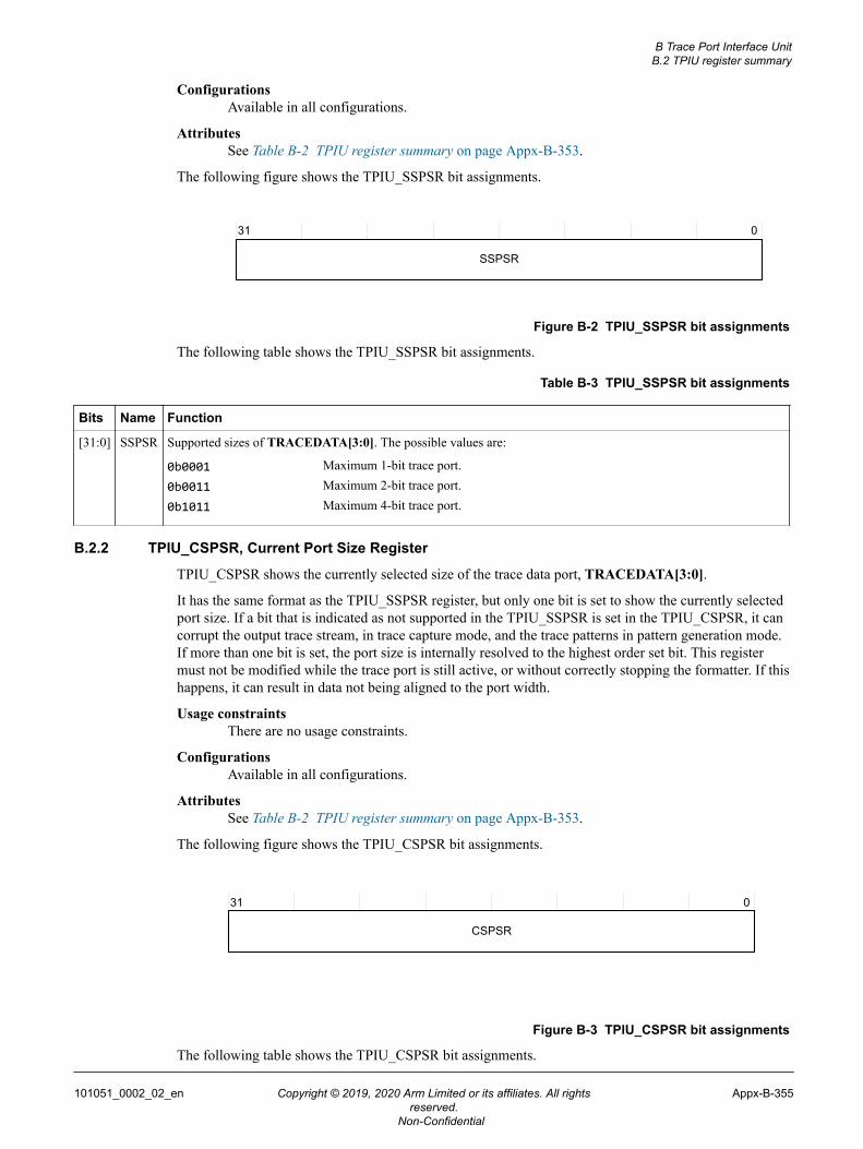
ConfigurationsAvailable in all configurations.
AttributesSee Table B-2 TPIU register summary on page Appx-B-353.
The following figure shows the TPIU_SSPSR bit assignments.
31 0
SSPSR
Figure B-2 TPIU_SSPSR bit assignments
The following table shows the TPIU_SSPSR bit assignments.
Table B-3 TPIU_SSPSR bit assignments
Bits Name Function
[31:0] SSPSR Supported sizes of TRACEDATA[3:0]. The possible values are:
0b0001 Maximum 1-bit trace port.0b0011 Maximum 2-bit trace port.0b1011 Maximum 4-bit trace port.
B.2.2 TPIU_CSPSR, Current Port Size Register
TPIU_CSPSR shows the currently selected size of the trace data port, TRACEDATA[3:0].
It has the same format as the TPIU_SSPSR register, but only one bit is set to show the currently selectedport size. If a bit that is indicated as not supported in the TPIU_SSPSR is set in the TPIU_CSPSR, it cancorrupt the output trace stream, in trace capture mode, and the trace patterns in pattern generation mode.If more than one bit is set, the port size is internally resolved to the highest order set bit. This registermust not be modified while the trace port is still active, or without correctly stopping the formatter. If thishappens, it can result in data not being aligned to the port width.
Usage constraintsThere are no usage constraints.
ConfigurationsAvailable in all configurations.
AttributesSee Table B-2 TPIU register summary on page Appx-B-353.
The following figure shows the TPIU_CSPSR bit assignments.
31 0
CSPSR
Figure B-3 TPIU_CSPSR bit assignments
The following table shows the TPIU_CSPSR bit assignments.
B Trace Port Interface UnitB.2 TPIU register summary
101051_0002_02_en Copyright © 2019, 2020 Arm Limited or its affiliates. All rightsreserved.
Appx-B-355
Non-Confidential
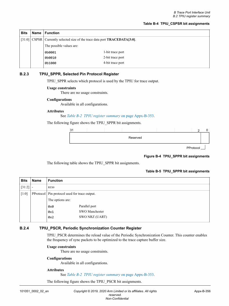
Table B-4 TPIU_CSPSR bit assignments
Bits Name Function
[31:0] CSPSR Currently selected size of the trace data port TRACEDATA[3:0].
The possible values are:
0b0001 1-bit trace port0b0010 2-bit trace port0b1000 4-bit trace port
B.2.3 TPIU_SPPR, Selected Pin Protocol Register
TPIU_SPPR selects which protocol is used by the TPIU for trace output.
Usage constraintsThere are no usage constraints.
ConfigurationsAvailable in all configurations.
AttributesSee Table B-2 TPIU register summary on page Appx-B-353.
The following figure shows the TPIU_SPPR bit assignments.
31 0
Reserved
2
PProtocol
Figure B-4 TPIU_SPPR bit assignments
The following table shows the TPIU_SPPR bit assignments.
Table B-5 TPIU_SPPR bit assignments
Bits Name Function
[31:2] - RES0
[1:0] PProtocol Pin protocol used for trace output.
The options are:
0x0 Parallel port0x1 SWO Manchester0x2 SWO NRZ (UART)
B.2.4 TPIU_PSCR, Periodic Synchronization Counter Register
TPIU_PSCR determines the reload value of the Periodic Synchronization Counter. This counter enablesthe frequency of sync packets to be optimized to the trace capture buffer size.
Usage constraintsThere are no usage constraints.
ConfigurationsAvailable in all configurations.
AttributesSee Table B-2 TPIU register summary on page Appx-B-353.
The following figure shows the TPIU_PSCR bit assignments.
B Trace Port Interface UnitB.2 TPIU register summary
101051_0002_02_en Copyright © 2019, 2020 Arm Limited or its affiliates. All rightsreserved.
Appx-B-356
Non-Confidential
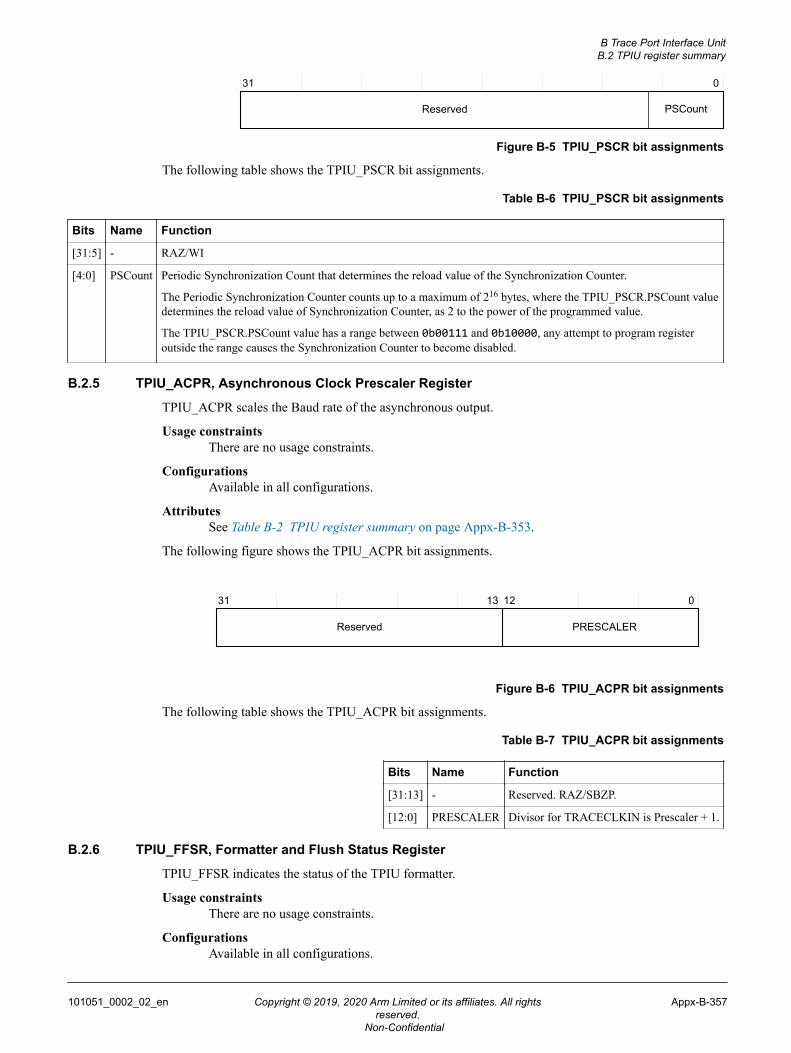
31 0
Reserved PSCount
Figure B-5 TPIU_PSCR bit assignments
The following table shows the TPIU_PSCR bit assignments.
Table B-6 TPIU_PSCR bit assignments
Bits Name Function
[31:5] - RAZ/WI
[4:0] PSCount Periodic Synchronization Count that determines the reload value of the Synchronization Counter.
The Periodic Synchronization Counter counts up to a maximum of 216 bytes, where the TPIU_PSCR.PSCount valuedetermines the reload value of Synchronization Counter, as 2 to the power of the programmed value.
The TPIU_PSCR.PSCount value has a range between 0b00111 and 0b10000, any attempt to program registeroutside the range causes the Synchronization Counter to become disabled.
B.2.5 TPIU_ACPR, Asynchronous Clock Prescaler Register
TPIU_ACPR scales the Baud rate of the asynchronous output.
Usage constraintsThere are no usage constraints.
ConfigurationsAvailable in all configurations.
AttributesSee Table B-2 TPIU register summary on page Appx-B-353.
The following figure shows the TPIU_ACPR bit assignments.
31 13 0
Reserved
12
PRESCALER
Figure B-6 TPIU_ACPR bit assignments
The following table shows the TPIU_ACPR bit assignments.
Table B-7 TPIU_ACPR bit assignments
Bits Name Function
[31:13] - Reserved. RAZ/SBZP.
[12:0] PRESCALER Divisor for TRACECLKIN is Prescaler + 1.
B.2.6 TPIU_FFSR, Formatter and Flush Status Register
TPIU_FFSR indicates the status of the TPIU formatter.
Usage constraintsThere are no usage constraints.
ConfigurationsAvailable in all configurations.
B Trace Port Interface UnitB.2 TPIU register summary
101051_0002_02_en Copyright © 2019, 2020 Arm Limited or its affiliates. All rightsreserved.
Appx-B-357
Non-Confidential
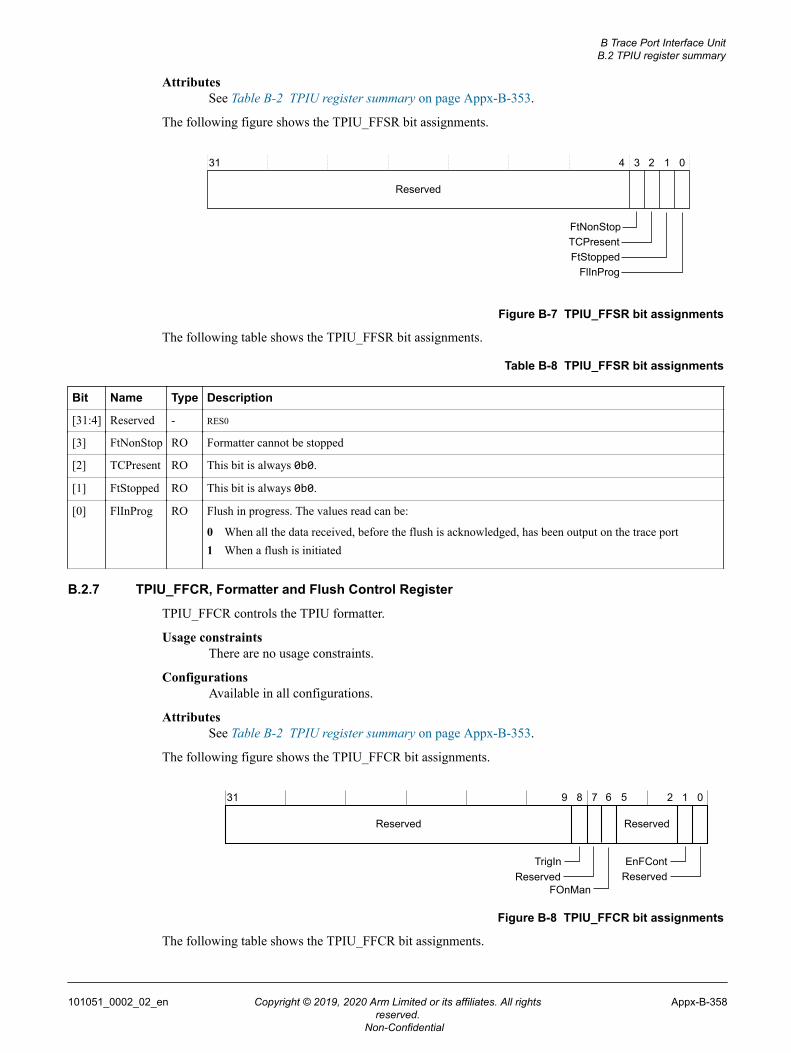
AttributesSee Table B-2 TPIU register summary on page Appx-B-353.
The following figure shows the TPIU_FFSR bit assignments.
31 2 0
Reserved
1
FlInProg
3
FtStoppedTCPresentFtNonStop
4
Figure B-7 TPIU_FFSR bit assignments
The following table shows the TPIU_FFSR bit assignments.
Table B-8 TPIU_FFSR bit assignments
Bit Name Type Description
[31:4] Reserved - RES0
[3] FtNonStop RO Formatter cannot be stopped
[2] TCPresent RO This bit is always 0b0.
[1] FtStopped RO This bit is always 0b0.
[0] FlInProg RO Flush in progress. The values read can be:
0 When all the data received, before the flush is acknowledged, has been output on the trace port1 When a flush is initiated
B.2.7 TPIU_FFCR, Formatter and Flush Control Register
TPIU_FFCR controls the TPIU formatter.
Usage constraintsThere are no usage constraints.
ConfigurationsAvailable in all configurations.
AttributesSee Table B-2 TPIU register summary on page Appx-B-353.
The following figure shows the TPIU_FFCR bit assignments.
Reserved
31 9 8 7 2 1 0
Reserved
TrigIn EnFContReservedReserved
FOnMan
6 5
Figure B-8 TPIU_FFCR bit assignments
The following table shows the TPIU_FFCR bit assignments.
B Trace Port Interface UnitB.2 TPIU register summary
101051_0002_02_en Copyright © 2019, 2020 Arm Limited or its affiliates. All rightsreserved.
Appx-B-358
Non-Confidential
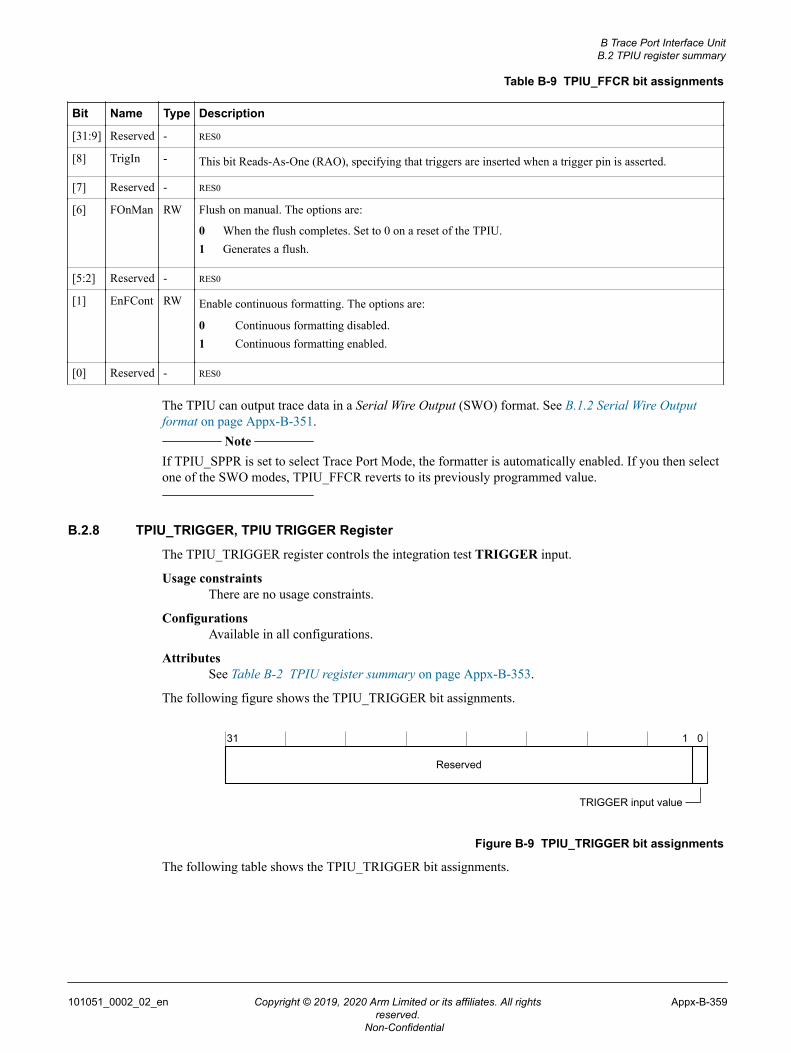
Table B-9 TPIU_FFCR bit assignments
Bit Name Type Description
[31:9] Reserved - RES0
[8] TrigIn - This bit Reads-As-One (RAO), specifying that triggers are inserted when a trigger pin is asserted.
[7] Reserved - RES0
[6] FOnMan RW Flush on manual. The options are:
0 When the flush completes. Set to 0 on a reset of the TPIU.1 Generates a flush.
[5:2] Reserved - RES0
[1] EnFCont RW Enable continuous formatting. The options are:
0 Continuous formatting disabled.1 Continuous formatting enabled.
[0] Reserved - RES0
The TPIU can output trace data in a Serial Wire Output (SWO) format. See B.1.2 Serial Wire Outputformat on page Appx-B-351.
Note
If TPIU_SPPR is set to select Trace Port Mode, the formatter is automatically enabled. If you then selectone of the SWO modes, TPIU_FFCR reverts to its previously programmed value.
B.2.8 TPIU_TRIGGER, TPIU TRIGGER Register
The TPIU_TRIGGER register controls the integration test TRIGGER input.
Usage constraintsThere are no usage constraints.
ConfigurationsAvailable in all configurations.
AttributesSee Table B-2 TPIU register summary on page Appx-B-353.
The following figure shows the TPIU_TRIGGER bit assignments.
Reserved
31 1 0
TRIGGER input value
Figure B-9 TPIU_TRIGGER bit assignments
The following table shows the TPIU_TRIGGER bit assignments.
B Trace Port Interface UnitB.2 TPIU register summary
101051_0002_02_en Copyright © 2019, 2020 Arm Limited or its affiliates. All rightsreserved.
Appx-B-359
Non-Confidential
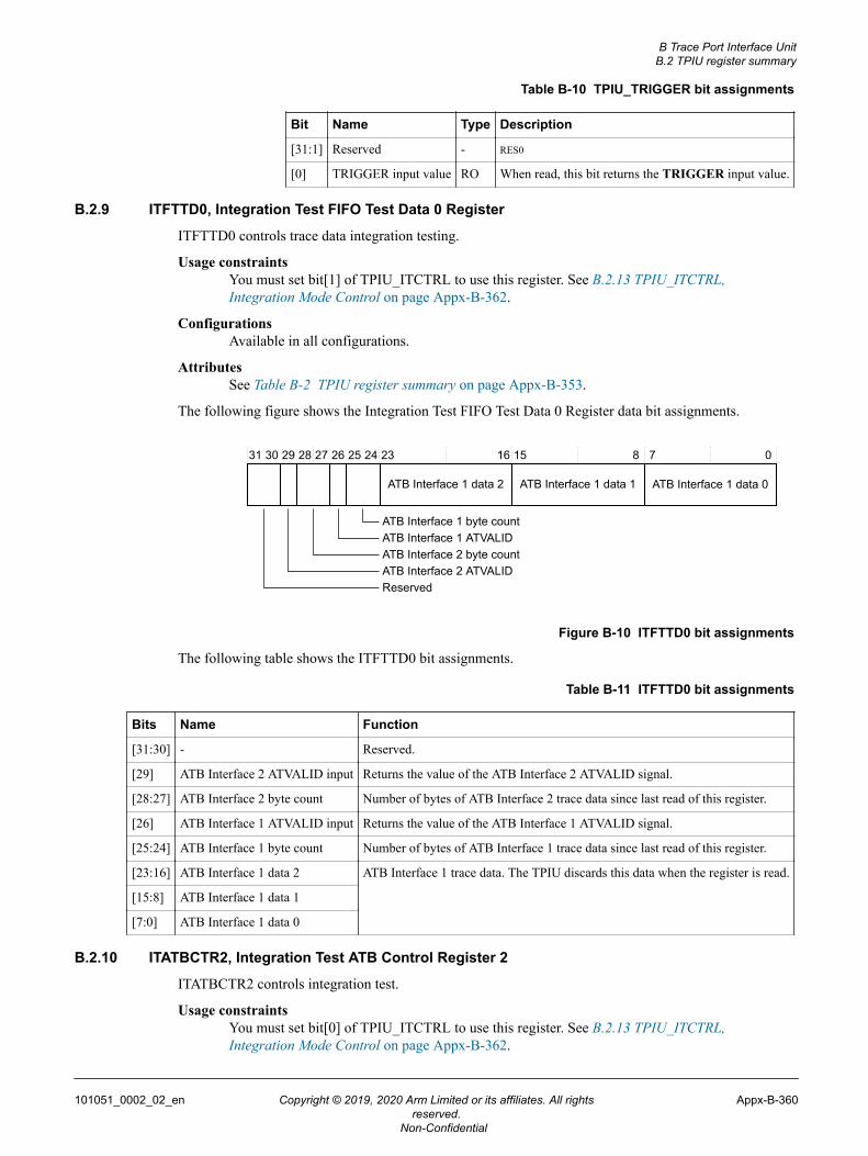
Table B-10 TPIU_TRIGGER bit assignments
Bit Name Type Description
[31:1] Reserved - RES0
[0] TRIGGER input value RO When read, this bit returns the TRIGGER input value.
B.2.9 ITFTTD0, Integration Test FIFO Test Data 0 Register
ITFTTD0 controls trace data integration testing.
Usage constraintsYou must set bit[1] of TPIU_ITCTRL to use this register. See B.2.13 TPIU_ITCTRL,Integration Mode Control on page Appx-B-362.
ConfigurationsAvailable in all configurations.
AttributesSee Table B-2 TPIU register summary on page Appx-B-353.
The following figure shows the Integration Test FIFO Test Data 0 Register data bit assignments.
ATB Interface 1 data 2 ATB Interface 1 data 1 ATB Interface 1 data 0
31 029 2728 26 2425 23 16 15 8 7
ATB Interface 1 byte countATB Interface 1 ATVALIDATB Interface 2 byte countATB Interface 2 ATVALID
30
Reserved
Figure B-10 ITFTTD0 bit assignments
The following table shows the ITFTTD0 bit assignments.
Table B-11 ITFTTD0 bit assignments
Bits Name Function
[31:30] - Reserved.
[29] ATB Interface 2 ATVALID input Returns the value of the ATB Interface 2 ATVALID signal.
[28:27] ATB Interface 2 byte count Number of bytes of ATB Interface 2 trace data since last read of this register.
[26] ATB Interface 1 ATVALID input Returns the value of the ATB Interface 1 ATVALID signal.
[25:24] ATB Interface 1 byte count Number of bytes of ATB Interface 1 trace data since last read of this register.
[23:16] ATB Interface 1 data 2 ATB Interface 1 trace data. The TPIU discards this data when the register is read.
[15:8] ATB Interface 1 data 1
[7:0] ATB Interface 1 data 0
B.2.10 ITATBCTR2, Integration Test ATB Control Register 2
ITATBCTR2 controls integration test.
Usage constraintsYou must set bit[0] of TPIU_ITCTRL to use this register. See B.2.13 TPIU_ITCTRL,Integration Mode Control on page Appx-B-362.
B Trace Port Interface UnitB.2 TPIU register summary
101051_0002_02_en Copyright © 2019, 2020 Arm Limited or its affiliates. All rightsreserved.
Appx-B-360
Non-Confidential
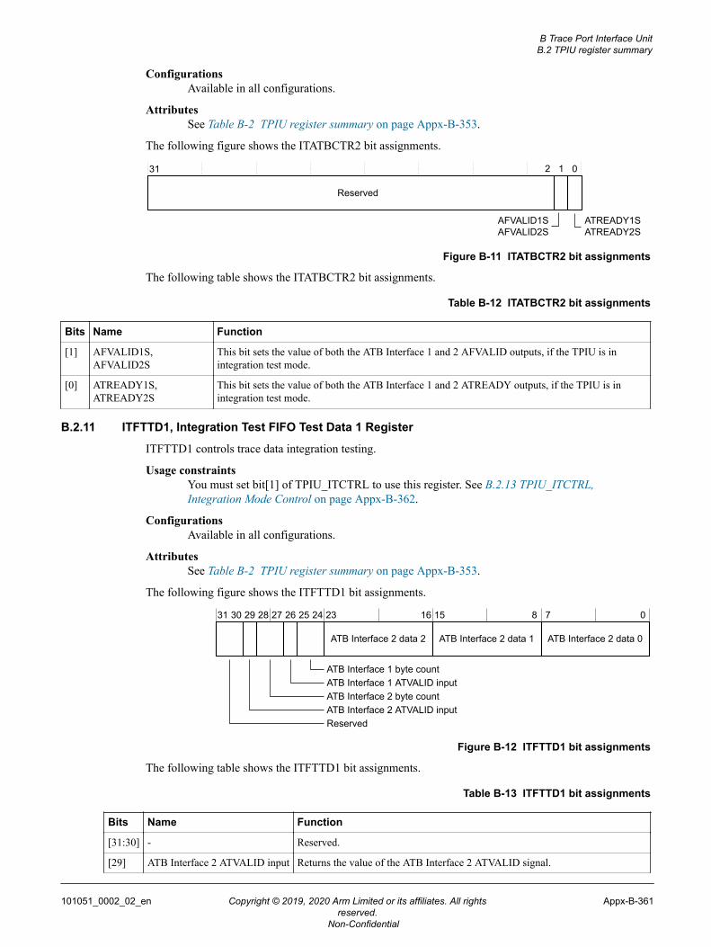
ConfigurationsAvailable in all configurations.
AttributesSee Table B-2 TPIU register summary on page Appx-B-353.
The following figure shows the ITATBCTR2 bit assignments.
31 0
Reserved
1
ATREADY1SATREADY2S
AFVALID1SAFVALID2S
2
Figure B-11 ITATBCTR2 bit assignments
The following table shows the ITATBCTR2 bit assignments.
Table B-12 ITATBCTR2 bit assignments
Bits Name Function
[1] AFVALID1S,AFVALID2S
This bit sets the value of both the ATB Interface 1 and 2 AFVALID outputs, if the TPIU is inintegration test mode.
[0] ATREADY1S,ATREADY2S
This bit sets the value of both the ATB Interface 1 and 2 ATREADY outputs, if the TPIU is inintegration test mode.
B.2.11 ITFTTD1, Integration Test FIFO Test Data 1 Register
ITFTTD1 controls trace data integration testing.
Usage constraintsYou must set bit[1] of TPIU_ITCTRL to use this register. See B.2.13 TPIU_ITCTRL,Integration Mode Control on page Appx-B-362.
ConfigurationsAvailable in all configurations.
AttributesSee Table B-2 TPIU register summary on page Appx-B-353.
The following figure shows the ITFTTD1 bit assignments.
31 30 29 28 27 26 25 24 23 16 15 8 7 0
ATB Interface 2 data 2 ATB Interface 2 data 1 ATB Interface 2 data 0
ATB Interface 1 byte countATB Interface 1 ATVALID inputATB Interface 2 byte countATB Interface 2 ATVALID inputReserved
Figure B-12 ITFTTD1 bit assignments
The following table shows the ITFTTD1 bit assignments.
Table B-13 ITFTTD1 bit assignments
Bits Name Function
[31:30] - Reserved.
[29] ATB Interface 2 ATVALID input Returns the value of the ATB Interface 2 ATVALID signal.
B Trace Port Interface UnitB.2 TPIU register summary
101051_0002_02_en Copyright © 2019, 2020 Arm Limited or its affiliates. All rightsreserved.
Appx-B-361
Non-Confidential
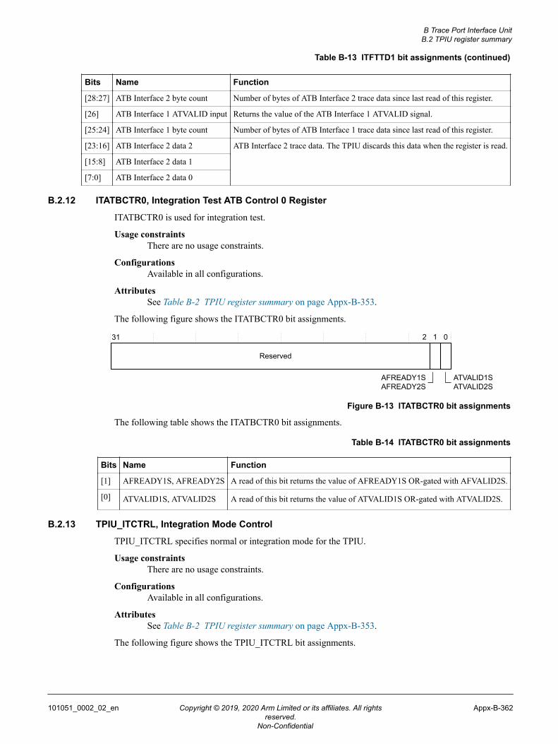
Table B-13 ITFTTD1 bit assignments (continued)
Bits Name Function
[28:27] ATB Interface 2 byte count Number of bytes of ATB Interface 2 trace data since last read of this register.
[26] ATB Interface 1 ATVALID input Returns the value of the ATB Interface 1 ATVALID signal.
[25:24] ATB Interface 1 byte count Number of bytes of ATB Interface 1 trace data since last read of this register.
[23:16] ATB Interface 2 data 2 ATB Interface 2 trace data. The TPIU discards this data when the register is read.
[15:8] ATB Interface 2 data 1
[7:0] ATB Interface 2 data 0
B.2.12 ITATBCTR0, Integration Test ATB Control 0 Register
ITATBCTR0 is used for integration test.
Usage constraintsThere are no usage constraints.
ConfigurationsAvailable in all configurations.
AttributesSee Table B-2 TPIU register summary on page Appx-B-353.
The following figure shows the ITATBCTR0 bit assignments.
31 0
Reserved
1
AFREADY1SAFREADY2S
ATVALID1SATVALID2S
2
Figure B-13 ITATBCTR0 bit assignments
The following table shows the ITATBCTR0 bit assignments.
Table B-14 ITATBCTR0 bit assignments
Bits Name Function
[1] AFREADY1S, AFREADY2S A read of this bit returns the value of AFREADY1S OR-gated with AFVALID2S.
[0] ATVALID1S, ATVALID2S A read of this bit returns the value of ATVALID1S OR-gated with ATVALID2S.
B.2.13 TPIU_ITCTRL, Integration Mode Control
TPIU_ITCTRL specifies normal or integration mode for the TPIU.
Usage constraintsThere are no usage constraints.
ConfigurationsAvailable in all configurations.
AttributesSee Table B-2 TPIU register summary on page Appx-B-353.
The following figure shows the TPIU_ITCTRL bit assignments.
B Trace Port Interface UnitB.2 TPIU register summary
101051_0002_02_en Copyright © 2019, 2020 Arm Limited or its affiliates. All rightsreserved.
Appx-B-362
Non-Confidential
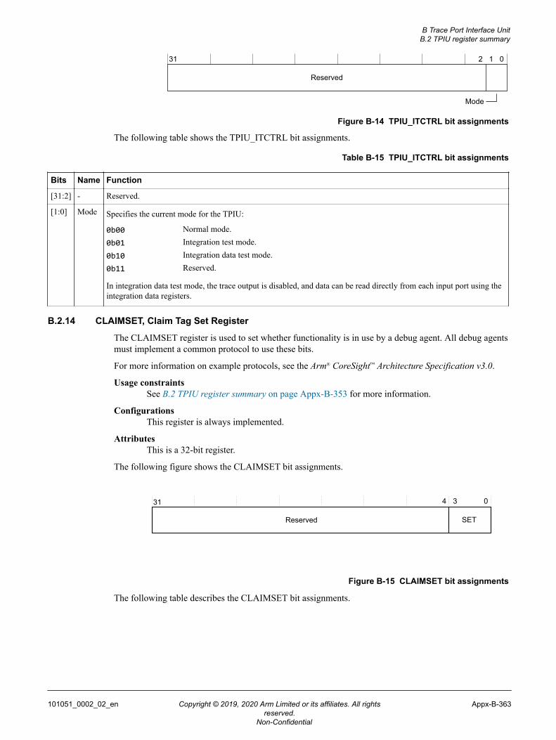
Reserved
31 2 1 0
Mode
Figure B-14 TPIU_ITCTRL bit assignments
The following table shows the TPIU_ITCTRL bit assignments.
Table B-15 TPIU_ITCTRL bit assignments
Bits Name Function
[31:2] - Reserved.
[1:0] Mode Specifies the current mode for the TPIU:
0b00 Normal mode.0b01 Integration test mode.0b10 Integration data test mode.0b11 Reserved.
In integration data test mode, the trace output is disabled, and data can be read directly from each input port using theintegration data registers.
B.2.14 CLAIMSET, Claim Tag Set Register
The CLAIMSET register is used to set whether functionality is in use by a debug agent. All debug agentsmust implement a common protocol to use these bits.
For more information on example protocols, see the Arm® CoreSight™ Architecture Specification v3.0.
Usage constraintsSee B.2 TPIU register summary on page Appx-B-353 for more information.
ConfigurationsThis register is always implemented.
AttributesThis is a 32-bit register.
The following figure shows the CLAIMSET bit assignments.
31 34
SETReserved
0
Figure B-15 CLAIMSET bit assignments
The following table describes the CLAIMSET bit assignments.
B Trace Port Interface UnitB.2 TPIU register summary
101051_0002_02_en Copyright © 2019, 2020 Arm Limited or its affiliates. All rightsreserved.
Appx-B-363
Non-Confidential
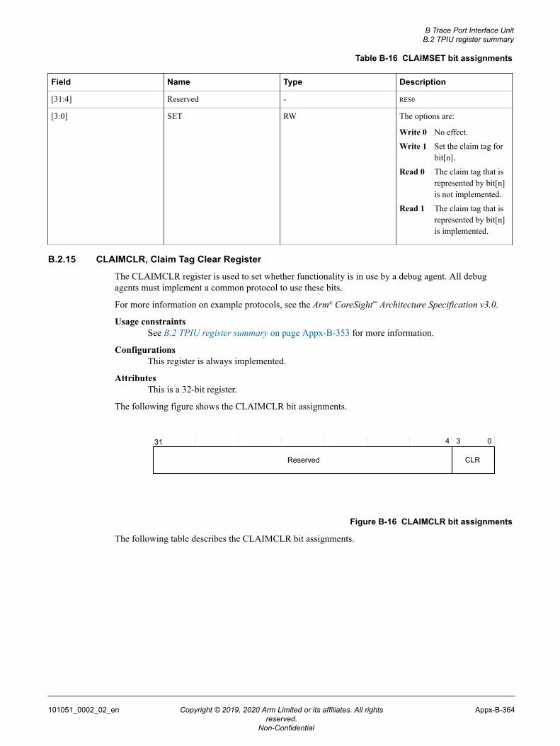
Table B-16 CLAIMSET bit assignments
Field Name Type Description
[31:4] Reserved - RES0
[3:0] SET RW The options are:
Write 0 No effect.
Write 1 Set the claim tag forbit[n].
Read 0 The claim tag that isrepresented by bit[n]is not implemented.
Read 1 The claim tag that isrepresented by bit[n]is implemented.
B.2.15 CLAIMCLR, Claim Tag Clear Register
The CLAIMCLR register is used to set whether functionality is in use by a debug agent. All debugagents must implement a common protocol to use these bits.
For more information on example protocols, see the Arm® CoreSight™ Architecture Specification v3.0.
Usage constraintsSee B.2 TPIU register summary on page Appx-B-353 for more information.
ConfigurationsThis register is always implemented.
AttributesThis is a 32-bit register.
The following figure shows the CLAIMCLR bit assignments.
31 34
CLRReserved
0
Figure B-16 CLAIMCLR bit assignments
The following table describes the CLAIMCLR bit assignments.
B Trace Port Interface UnitB.2 TPIU register summary
101051_0002_02_en Copyright © 2019, 2020 Arm Limited or its affiliates. All rightsreserved.
Appx-B-364
Non-Confidential
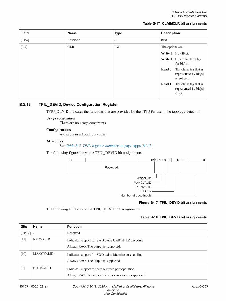
Table B-17 CLAIMCLR bit assignments
Field Name Type Description
[31:4] Reserved - RES0
[3:0] CLR RW The options are:
Write 0 No effect.
Write 1 Clear the claim tagfor bit[n].
Read 0 The claim tag that isrepresented by bit[n]is not set.
Read 1 The claim tag that isrepresented by bit[n]is set.
B.2.16 TPIU_DEVID, Device Configuration Register
TPIU_DEVID indicates the functions that are provided by the TPIU for use in the topology detection.
Usage constraintsThere are no usage constraints.
ConfigurationsAvailable in all configurations.
AttributesSee Table B-2 TPIU register summary on page Appx-B-353.
The following figure shows the TPIU_DEVID bit assignments.
Reserved
31 12 11 10 9 8 6 5 0
NRZVALIDMANCVALID
PTINVALID FIFOSZ
Number of trace inputs
Figure B-17 TPIU_DEVID bit assignments
The following table shows the TPIU_DEVID bit assignments.
Table B-18 TPIU_DEVID bit assignments
Bits Name Function
[31:12] - Reserved.
[11] NRZVALID Indicates support for SWO using UART/NRZ encoding.
Always RAO. The output is supported.
[10] MANCVALID Indicates support for SWO using Manchester encoding.
Always RAO. The output is supported.
[9] PTINVALID Indicates support for parallel trace port operation.
Always RAZ. Trace data and clock modes are supported.
B Trace Port Interface UnitB.2 TPIU register summary
101051_0002_02_en Copyright © 2019, 2020 Arm Limited or its affiliates. All rightsreserved.
Appx-B-365
Non-Confidential
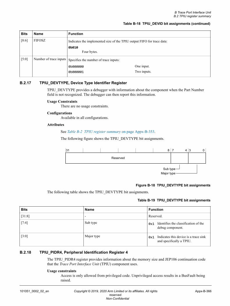
Table B-18 TPIU_DEVID bit assignments (continued)
Bits Name Function
[8:6] FIFOSZ Indicates the implemented size of the TPIU output FIFO for trace data:
0b010Four bytes.
[5:0] Number of trace inputs Specifies the number of trace inputs:
0b000000 One input.0b000001 Two inputs.
B.2.17 TPIU_DEVTYPE, Device Type Identifier Register
TPIU_DEVTYPE provides a debugger with information about the component when the Part Numberfield is not recognized. The debugger can then report this information.
Usage ConstraintsThere are no usage constraints.
ConfigurationsAvailable in all configurations.
Attributes
See Table B-2 TPIU register summary on page Appx-B-353.
The following figure shows the TPIU_DEVTYPE bit assignments.
Reserved
31 78 0
Sub type
4
Major type
3
Figure B-18 TPIU_DEVTYPE bit assignments
The following table shows the TPIU_DEVTYPE bit assignments.
Table B-19 TPIU_DEVTYPE bit assignments
Bits Name Function
[31:8] - Reserved.
[7:4] Sub type 0x1 Identifies the classification of thedebug component.
[3:0] Major type 0x1 Indicates this device is a trace sinkand specifically a TPIU.
B.2.18 TPIU_PIDR4, Peripheral Identification Register 4
The TPIU_PIDR4 register provides information about the memory size and JEP106 continuation codethat the Trace Port Interface Unit (TPIU) component uses.
Usage constraintsAccess is only allowed from privileged code. Unprivileged access results in a BusFault beingraised.
B Trace Port Interface UnitB.2 TPIU register summary
101051_0002_02_en Copyright © 2019, 2020 Arm Limited or its affiliates. All rightsreserved.
Appx-B-366
Non-Confidential
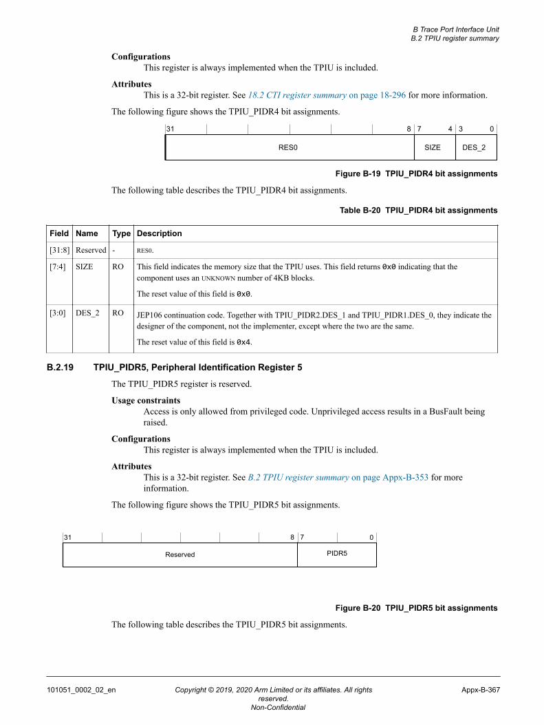
ConfigurationsThis register is always implemented when the TPIU is included.
AttributesThis is a 32-bit register. See 18.2 CTI register summary on page 18-296 for more information.
The following figure shows the TPIU_PIDR4 bit assignments.
31 8 7 4 3 0
DES_2SIZERES0
Figure B-19 TPIU_PIDR4 bit assignments
The following table describes the TPIU_PIDR4 bit assignments.
Table B-20 TPIU_PIDR4 bit assignments
Field Name Type Description
[31:8] Reserved - RES0.
[7:4] SIZE RO This field indicates the memory size that the TPIU uses. This field returns 0x0 indicating that thecomponent uses an UNKNOWN number of 4KB blocks.
The reset value of this field is 0x0.
[3:0] DES_2 RO JEP106 continuation code. Together with TPIU_PIDR2.DES_1 and TPIU_PIDR1.DES_0, they indicate thedesigner of the component, not the implementer, except where the two are the same.
The reset value of this field is 0x4.
B.2.19 TPIU_PIDR5, Peripheral Identification Register 5
The TPIU_PIDR5 register is reserved.
Usage constraintsAccess is only allowed from privileged code. Unprivileged access results in a BusFault beingraised.
ConfigurationsThis register is always implemented when the TPIU is included.
AttributesThis is a 32-bit register. See B.2 TPIU register summary on page Appx-B-353 for moreinformation.
The following figure shows the TPIU_PIDR5 bit assignments.
31 8 7 0
Reserved PIDR5
Figure B-20 TPIU_PIDR5 bit assignments
The following table describes the TPIU_PIDR5 bit assignments.
B Trace Port Interface UnitB.2 TPIU register summary
101051_0002_02_en Copyright © 2019, 2020 Arm Limited or its affiliates. All rightsreserved.
Appx-B-367
Non-Confidential
Table B-21 TPIU_PIDR5 bit assignments
Field Name Type Description
[31:8] Reserved - RES0.
[7:0] PIDR5 RO RES0.
B.2.20 TPIU_PIDR6, Peripheral Identification Register 6
The TPIU_PIDR6 register is reserved.
Usage constraintsAccess is only allowed from privileged code. Unprivileged access results in a BusFault beingraised.
ConfigurationsThis register is always implemented when the TPIU is included.
AttributesThis is a 32-bit register. See B.2 TPIU register summary on page Appx-B-353 for moreinformation.
The following figure shows the TPIU_PIDR6 bit assignments.
31 8 7 0
Reserved PIDR6
Figure B-21 TPIU_PIDR6 bit assignments
The following table describes the TPIU_PIDR6 bit assignments.
Table B-22 TPIU_PIDR6 bit assignments
Field Name Type Description
[31:8] Reserved - RES0.
[7:0] PIDR6 RO RES0.
B.2.21 TPIU_PIDR7, Peripheral Identification Register 7
The TPIU_PIDR7 register is reserved.
Usage constraintsAccess is only allowed from privileged code. Unprivileged access results in a BusFault beingraised.
ConfigurationsThis register is always implemented when the TPIU is included.
AttributesThis is a 32-bit register. See B.2 TPIU register summary on page Appx-B-353 for moreinformation.
The following figure shows the TPIU_PIDR7 bit assignments.
B Trace Port Interface UnitB.2 TPIU register summary
101051_0002_02_en Copyright © 2019, 2020 Arm Limited or its affiliates. All rightsreserved.
Appx-B-368
Non-Confidential
31 8 7 0
Reserved PIDR7
Figure B-22 TPIU_PIDR7 bit assignments
The following table describes the TPIU_PIDR7 bit assignments.
Table B-23 TPIU_PIDR7 bit assignments
Field Name Type Description
[31:8] Reserved - RES0.
[7:0] PIDR7 RO RES0.
B.2.22 TPIU_PIDR0, Peripheral Identification Register 0
The TPIU_PIDR0 register indicates the TPIU component part number.
Usage constraintsAccess is only allowed from privileged code. Unprivileged access results in a BusFault beingraised.
ConfigurationsThis register is always implemented when the TPIU is included.
AttributesThis is a 32-bit register. See B.2 TPIU register summary on page Appx-B-353 for moreinformation.
The following figure shows the TPIU_PIDR0 bit assignments.
31 8 7 0
Reserved PART_0
Figure B-23 TPIU_PIDR0 bit assignments
The following table describes the TPIU_PIDR0 bit assignments.
Table B-24 TPIU_PIDR0 bit assignments
Field Name Type Description
[31:8] Reserved - RES0.
[7:0] PART_0 RO This field indicates the part number. When taken together with TPIU_PIDR1.PART_1, it indicates thecomponent. The part number is selected by the designer of the component.
The reset value of this field is 0b00100010.
B Trace Port Interface UnitB.2 TPIU register summary
101051_0002_02_en Copyright © 2019, 2020 Arm Limited or its affiliates. All rightsreserved.
Appx-B-369
Non-Confidential
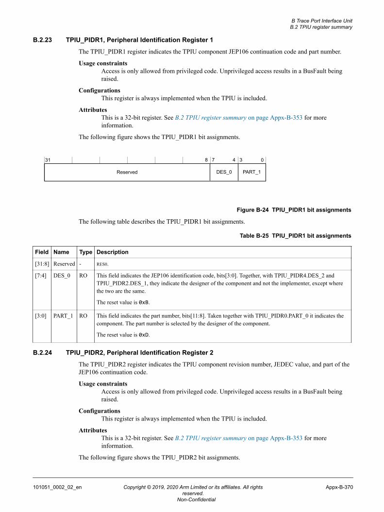
B.2.23 TPIU_PIDR1, Peripheral Identification Register 1
The TPIU_PIDR1 register indicates the TPIU component JEP106 continuation code and part number.
Usage constraintsAccess is only allowed from privileged code. Unprivileged access results in a BusFault beingraised.
ConfigurationsThis register is always implemented when the TPIU is included.
AttributesThis is a 32-bit register. See B.2 TPIU register summary on page Appx-B-353 for moreinformation.
The following figure shows the TPIU_PIDR1 bit assignments.
31 8 7 0
Reserved PART_1DES_0
4 3
Figure B-24 TPIU_PIDR1 bit assignments
The following table describes the TPIU_PIDR1 bit assignments.
Table B-25 TPIU_PIDR1 bit assignments
Field Name Type Description
[31:8] Reserved - RES0.
[7:4] DES_0 RO This field indicates the JEP106 identification code, bits[3:0]. Together, with TPIU_PIDR4.DES_2 andTPIU_PIDR2.DES_1, they indicate the designer of the component and not the implementer, except wherethe two are the same.
The reset value is 0xB.
[3:0] PART_1 RO This field indicates the part number, bits[11:8]. Taken together with TPIU_PIDR0.PART_0 it indicates thecomponent. The part number is selected by the designer of the component.
The reset value is 0xD.
B.2.24 TPIU_PIDR2, Peripheral Identification Register 2
The TPIU_PIDR2 register indicates the TPIU component revision number, JEDEC value, and part of theJEP106 continuation code.
Usage constraintsAccess is only allowed from privileged code. Unprivileged access results in a BusFault beingraised.
ConfigurationsThis register is always implemented when the TPIU is included.
AttributesThis is a 32-bit register. See B.2 TPIU register summary on page Appx-B-353 for moreinformation.
The following figure shows the TPIU_PIDR2 bit assignments.
B Trace Port Interface UnitB.2 TPIU register summary
101051_0002_02_en Copyright © 2019, 2020 Arm Limited or its affiliates. All rightsreserved.
Appx-B-370
Non-Confidential
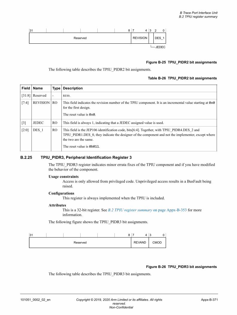
31 8 7 0
Reserved DES_1REVISION
4 3 2
JEDEC
Figure B-25 TPIU_PIDR2 bit assignments
The following table describes the TPIU_PIDR2 bit assignments.
Table B-26 TPIU_PIDR2 bit assignments
Field Name Type Description
[31:8] Reserved - RES0.
[7:4] REVISION RO This field indicates the revision number of the TPIU component. It is an incremental value starting at 0x0for the first design.
The reset value is 0x0.
[3] JEDEC RO This field is always 1, indicating that a JEDEC assigned value is used.
[2:0] DES_1 RO This field is the JEP106 identification code, bits[6:4]. Together, with TPIU_PIDR4.DES_2 andTPIU_PIDR1.DES_0, they indicate the designer of the component and not the implementer, except wherethe two are the same.
The reset value is 0b011.
B.2.25 TPIU_PIDR3, Peripheral Identification Register 3
The TPIU_PIDR3 register indicates minor errata fixes of the TPIU component and if you have modifiedthe behavior of the component.
Usage constraintsAccess is only allowed from privileged code. Unprivileged access results in a BusFault beingraised.
ConfigurationsThis register is always implemented when the TPIU is included.
AttributesThis is a 32-bit register. See B.2 TPIU register summary on page Appx-B-353 for moreinformation.
The following figure shows the TPIU_PIDR3 bit assignments.
31 8 7 0
Reserved CMODREVAND
4 3
Figure B-26 TPIU_PIDR3 bit assignments
The following table describes the TPIU_PIDR3 bit assignments.
B Trace Port Interface UnitB.2 TPIU register summary
101051_0002_02_en Copyright © 2019, 2020 Arm Limited or its affiliates. All rightsreserved.
Appx-B-371
Non-Confidential
Table B-27 TPIU_PIDR3 bit assignments
Field Name Type Description
[31:8] Reserved - RES0.
[7:4] REVAND RO This field indicates minor errata fixes specific to this design, for example metal fixes after implementation.In most cases this field is 0x0.
[3:0] CMOD RO Customer modified. Where the component is reusable IP, this value indicates whether you have modifiedthe behavior of the component. In most cases, this field is 0x0.
B.2.26 TPIU_ CIDR0, Component Identification Register 0
The TPIU_CIDR0 register indicates the preamble.
Usage constraintsAccess is only allowed from privileged code. Unprivileged access results in a BusFault beingraised.
ConfigurationsThis register is always implemented when the TPIU is included.
AttributesThis is a 32-bit register. See B.2 TPIU register summary on page Appx-B-353 for moreinformation.
The following figure shows the TPIU_CIDR0 bit assignments.
31 8 7 0
Reserved PRMBL_0
Figure B-27 TPIU_CIDR0 bit assignments
The following table describes the TPIU_CIDR0 bit assignments.
Table B-28 TPIU_CIDR0 bit assignments
Field Name Type Description
[31:8] Reserved - RES0.
[7:0] PRMBL_0 RO Preamble. This field returns 0x0D.
B.2.27 TPIU_ CIDR1, Component Identification Register 1
The TPIU_CIDR1 register indicates the component class and preamble.
Usage constraintsAccess is only allowed from privileged code. Unprivileged access results in a BusFault beingraised.
ConfigurationsThis register is always implemented when the TPIU is included.
AttributesThis is a 32-bit register. See B.2 TPIU register summary on page Appx-B-353 for moreinformation.
B Trace Port Interface UnitB.2 TPIU register summary
101051_0002_02_en Copyright © 2019, 2020 Arm Limited or its affiliates. All rightsreserved.
Appx-B-372
Non-Confidential
The following figure shows the TPIU_CIDR1 bit assignments.
31 8 7 0
Reserved PRMBL_1CLASS
4 3
Figure B-28 TPIU_CIDR1 bit assignments
The following table describes the TPIU_CIDR1 bit assignments.
Table B-29 TPIU_CIDR1 bit assignments
Field Name Type Description
[31:8] Reserved - RES0.
[7:4] CLASS RO Component class. Returns 0x9, indicating this is a CoreSight component.
[3:0] PRMBL_1 RO Preamble. This field returns 0x0.
B.2.28 TPIU_ CIDR2, Component Identification Register 2
The TPIU_CIDR2 register indicates the preamble.
Usage constraintsAccess is only allowed from privileged code. Unprivileged access results in a BusFault beingraised.
ConfigurationsThis register is always implemented when the TPIU is included.
AttributesThis is a 32-bit register. See B.2 TPIU register summary on page Appx-B-353 for moreinformation.
The following figure shows the TPIU_CIDR2 bit assignments.
31 8 7 0
Reserved PRMBL_2
Figure B-29 TPIU_CIDR2 bit assignments
The following table describes the TPIU_CIDR2 bit assignments.
Table B-30 TPIU_CIDR2 bit assignments
Field Name Type Description
[31:8] Reserved - RES0.
[7:0] PRMBL_2 RO Preamble. This field returns 0x05.
B.2.29 TPIU_ CIDR3, Component Identification Register 3
The TPIU_CIDR3 register indicates the preamble.
B Trace Port Interface UnitB.2 TPIU register summary
101051_0002_02_en Copyright © 2019, 2020 Arm Limited or its affiliates. All rightsreserved.
Appx-B-373
Non-Confidential
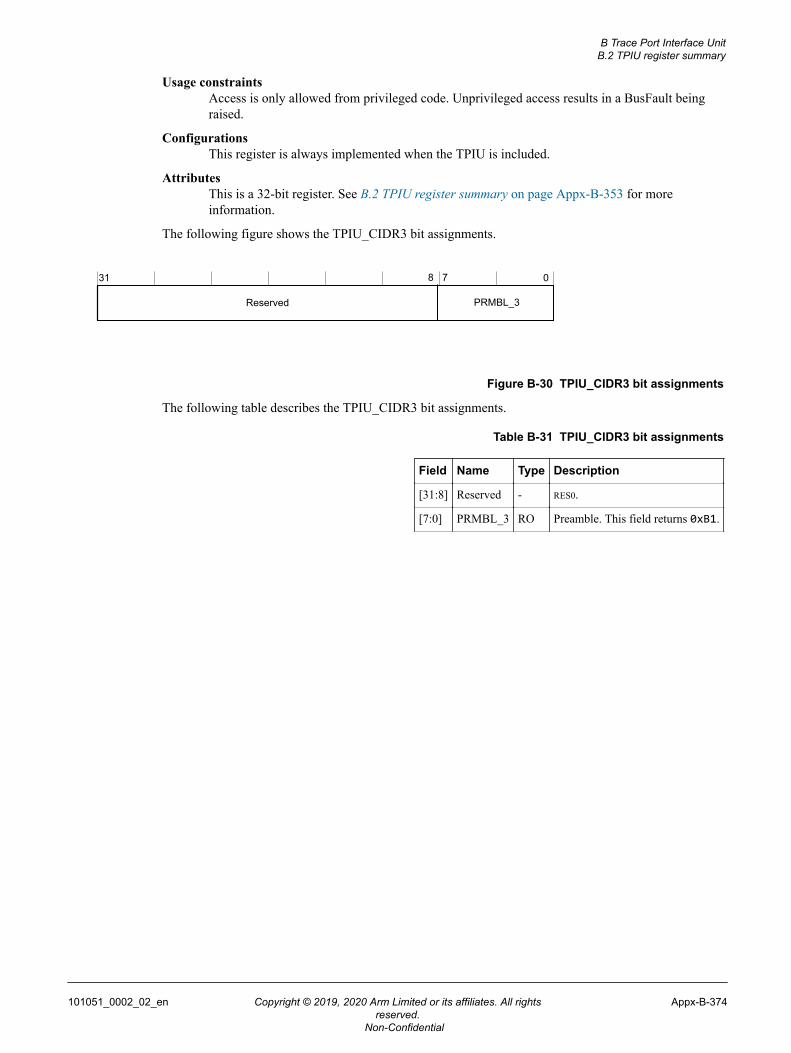
Usage constraintsAccess is only allowed from privileged code. Unprivileged access results in a BusFault beingraised.
ConfigurationsThis register is always implemented when the TPIU is included.
AttributesThis is a 32-bit register. See B.2 TPIU register summary on page Appx-B-353 for moreinformation.
The following figure shows the TPIU_CIDR3 bit assignments.
31 8 7 0
Reserved PRMBL_3
Figure B-30 TPIU_CIDR3 bit assignments
The following table describes the TPIU_CIDR3 bit assignments.
Table B-31 TPIU_CIDR3 bit assignments
Field Name Type Description
[31:8] Reserved - RES0.
[7:0] PRMBL_3 RO Preamble. This field returns 0xB1.
B Trace Port Interface UnitB.2 TPIU register summary
101051_0002_02_en Copyright © 2019, 2020 Arm Limited or its affiliates. All rightsreserved.
Appx-B-374
Non-Confidential
Appendix CSignal descriptions
This appendix describes the Cortex-M55 processor signals.
It contains the following sections:• C.1 Clock and clock enable signals on page Appx-C-377.• C.2 Reset signals on page Appx-C-378.• C.3 Static configuration signals on page Appx-C-379.• C.4 Reset configuration signals on page Appx-C-381.• C.5 Cache initialization signal on page Appx-C-382.• C.6 Instruction execution control signals on page Appx-C-383.• C.7 Instruction Tightly Coupled Memory interface signals on page Appx-C-384.• C.8 Data Tightly Coupled Memory interface signals on page Appx-C-386.• C.9 M-AXI interface signals on page Appx-C-388.• C.10 S-AHB interface signals on page Appx-C-392.• C.11 P-AHB interface signals on page Appx-C-394.• C.12 D-AHB interface signals on page Appx-C-396.• C.13 EPPB interface signals on page Appx-C-398.• C.14 External coprocessor interface signals on page Appx-C-399.• C.15 Debug interface signals on page Appx-C-400.• C.16 P-Channel and Q-Channel power control signals on page Appx-C-401.• C.17 Q-Channel clock control signals on page Appx-C-402.• C.18 Power compatibility control signals on page Appx-C-403.• C.19 ITM interface signals on page Appx-C-404.• C.20 ETM interface signals on page Appx-C-405.• C.21 Trace synchronization and trigger signals on page Appx-C-406.• C.22 CTI interface signals on page Appx-C-407.• C.23 Interrupt signals on page Appx-C-408.
101051_0002_02_en Copyright © 2019, 2020 Arm Limited or its affiliates. All rightsreserved.
Appx-C-375
Non-Confidential
• C.24 WIC interface signals on page Appx-C-409.• C.25 Event signals on page Appx-C-411.• C.26 IDAU interface signals on page Appx-C-412.• C.27 Miscellaneous signals on page Appx-C-413.• C.28 Error interface signals on page Appx-C-417.• C.29 Floating-point exception signals on page Appx-C-418.• C.30 Test interface signals on page Appx-C-419.• C.31 Reserved signals on page Appx-C-420.
C Signal descriptions
101051_0002_02_en Copyright © 2019, 2020 Arm Limited or its affiliates. All rightsreserved.
Appx-C-376
Non-Confidential
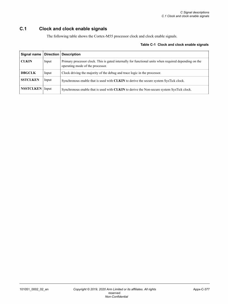
C.1 Clock and clock enable signalsThe following table shows the Cortex-M55 processor clock and clock enable signals.
Table C-1 Clock and clock enable signals
Signal name Direction Description
CLKIN Input Primary processor clock. This is gated internally for functional units when required depending on theoperating mode of the processor.
DBGCLK Input Clock driving the majority of the debug and trace logic in the processor.
SSTCLKEN Input Synchronous enable that is used with CLKIN to derive the secure system SysTick clock.
NSSTCLKEN Input Synchronous enable that is used with CLKIN to derive the Non-secure system SysTick clock.
C Signal descriptionsC.1 Clock and clock enable signals
101051_0002_02_en Copyright © 2019, 2020 Arm Limited or its affiliates. All rightsreserved.
Appx-C-377
Non-Confidential
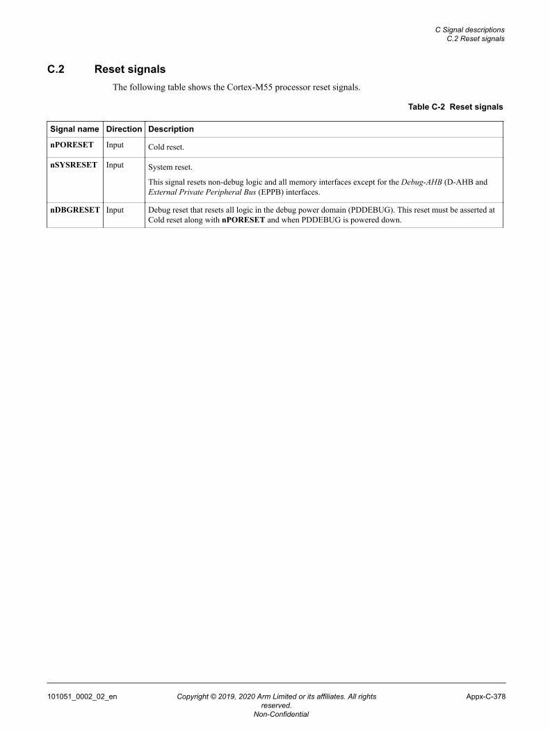
C.2 Reset signalsThe following table shows the Cortex-M55 processor reset signals.
Table C-2 Reset signals
Signal name Direction Description
nPORESET Input Cold reset.
nSYSRESET Input System reset.
This signal resets non-debug logic and all memory interfaces except for the Debug-AHB (D-AHB andExternal Private Peripheral Bus (EPPB) interfaces.
nDBGRESET Input Debug reset that resets all logic in the debug power domain (PDDEBUG). This reset must be asserted atCold reset along with nPORESET and when PDDEBUG is powered down.
C Signal descriptionsC.2 Reset signals
101051_0002_02_en Copyright © 2019, 2020 Arm Limited or its affiliates. All rightsreserved.
Appx-C-378
Non-Confidential
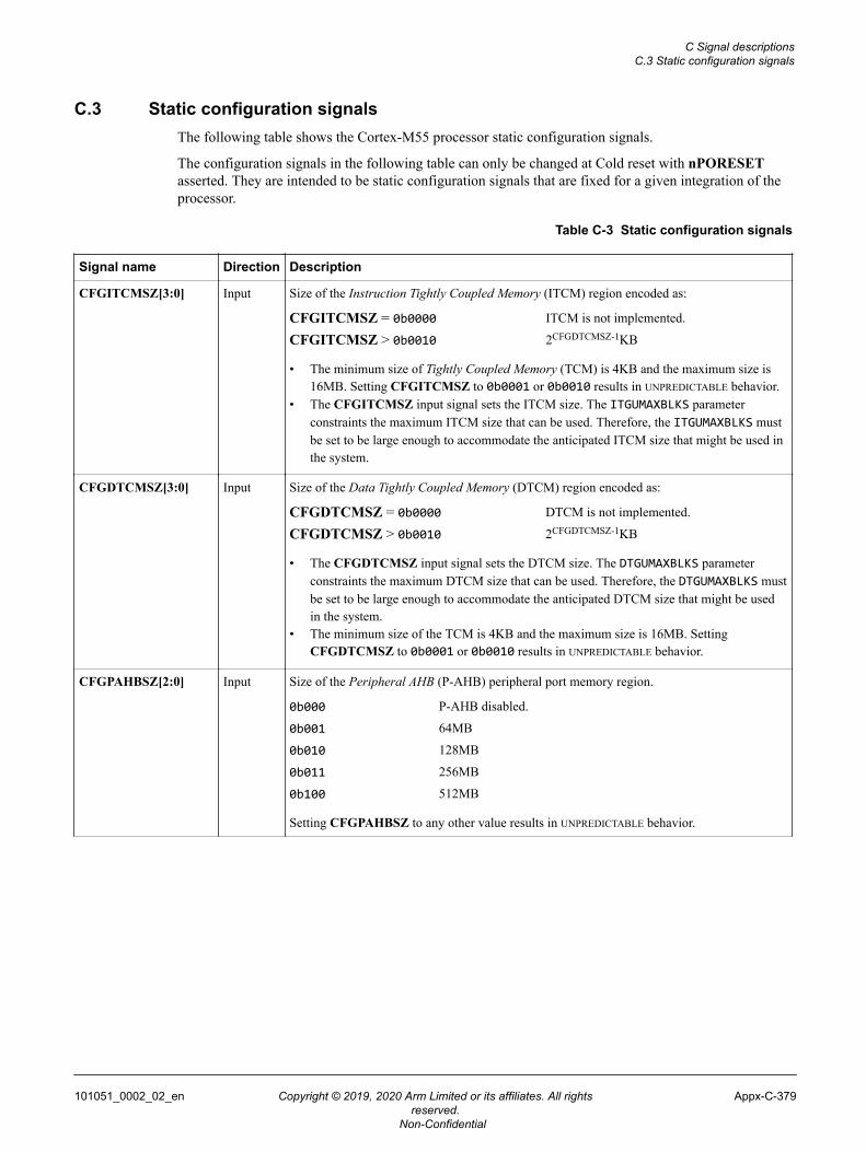
C.3 Static configuration signalsThe following table shows the Cortex-M55 processor static configuration signals.
The configuration signals in the following table can only be changed at Cold reset with nPORESETasserted. They are intended to be static configuration signals that are fixed for a given integration of theprocessor.
Table C-3 Static configuration signals
Signal name Direction Description
CFGITCMSZ[3:0] Input Size of the Instruction Tightly Coupled Memory (ITCM) region encoded as:
CFGITCMSZ = 0b0000 ITCM is not implemented.
CFGITCMSZ > 0b0010 2CFGDTCMSZ-1KB
• The minimum size of Tightly Coupled Memory (TCM) is 4KB and the maximum size is16MB. Setting CFGITCMSZ to 0b0001 or 0b0010 results in UNPREDICTABLE behavior.
• The CFGITCMSZ input signal sets the ITCM size. The ITGUMAXBLKS parameterconstraints the maximum ITCM size that can be used. Therefore, the ITGUMAXBLKS mustbe set to be large enough to accommodate the anticipated ITCM size that might be used inthe system.
CFGDTCMSZ[3:0] Input Size of the Data Tightly Coupled Memory (DTCM) region encoded as:
CFGDTCMSZ = 0b0000 DTCM is not implemented.
CFGDTCMSZ > 0b0010 2CFGDTCMSZ-1KB
• The CFGDTCMSZ input signal sets the DTCM size. The DTGUMAXBLKS parameterconstraints the maximum DTCM size that can be used. Therefore, the DTGUMAXBLKS mustbe set to be large enough to accommodate the anticipated DTCM size that might be usedin the system.
• The minimum size of the TCM is 4KB and the maximum size is 16MB. SettingCFGDTCMSZ to 0b0001 or 0b0010 results in UNPREDICTABLE behavior.
CFGPAHBSZ[2:0] Input Size of the Peripheral AHB (P-AHB) peripheral port memory region.
0b000 P-AHB disabled.
0b001 64MB
0b010 128MB
0b011 256MB
0b100 512MB
Setting CFGPAHBSZ to any other value results in UNPREDICTABLE behavior.
C Signal descriptionsC.3 Static configuration signals
101051_0002_02_en Copyright © 2019, 2020 Arm Limited or its affiliates. All rightsreserved.
Appx-C-379
Non-Confidential
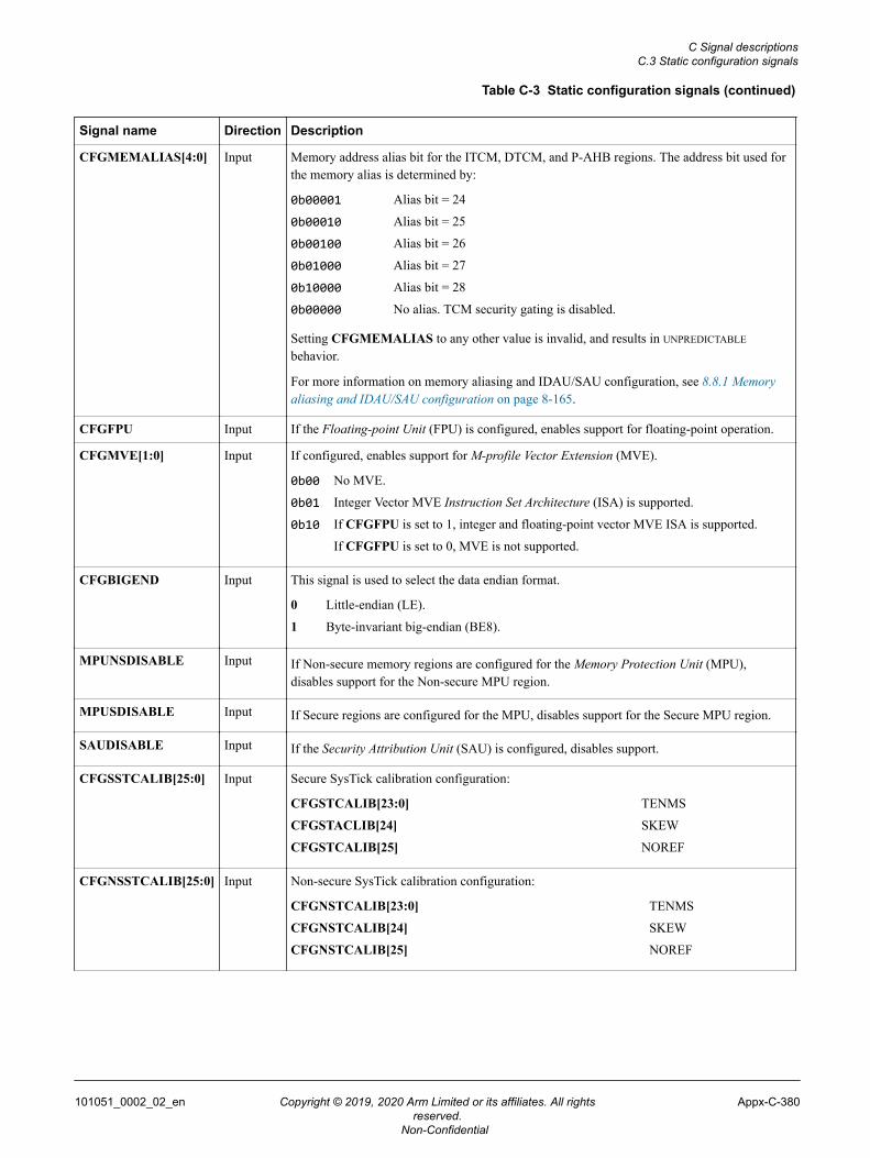
Table C-3 Static configuration signals (continued)
Signal name Direction Description
CFGMEMALIAS[4:0] Input Memory address alias bit for the ITCM, DTCM, and P-AHB regions. The address bit used forthe memory alias is determined by:
0b00001 Alias bit = 24
0b00010 Alias bit = 25
0b00100 Alias bit = 26
0b01000 Alias bit = 27
0b10000 Alias bit = 28
0b00000 No alias. TCM security gating is disabled.
Setting CFGMEMALIAS to any other value is invalid, and results in UNPREDICTABLE
behavior.
For more information on memory aliasing and IDAU/SAU configuration, see 8.8.1 Memoryaliasing and IDAU/SAU configuration on page 8-165.
CFGFPU Input If the Floating-point Unit (FPU) is configured, enables support for floating-point operation.
CFGMVE[1:0] Input If configured, enables support for M-profile Vector Extension (MVE).
0b00 No MVE.
0b01 Integer Vector MVE Instruction Set Architecture (ISA) is supported.
0b10 If CFGFPU is set to 1, integer and floating-point vector MVE ISA is supported.
If CFGFPU is set to 0, MVE is not supported.
CFGBIGEND Input This signal is used to select the data endian format.
0 Little-endian (LE).
1 Byte-invariant big-endian (BE8).
MPUNSDISABLE Input If Non-secure memory regions are configured for the Memory Protection Unit (MPU),disables support for the Non-secure MPU region.
MPUSDISABLE Input If Secure regions are configured for the MPU, disables support for the Secure MPU region.
SAUDISABLE Input If the Security Attribution Unit (SAU) is configured, disables support.
CFGSSTCALIB[25:0] Input Secure SysTick calibration configuration:
CFGSTCALIB[23:0] TENMS
CFGSTACLIB[24] SKEW
CFGSTCALIB[25] NOREF
CFGNSSTCALIB[25:0] Input Non-secure SysTick calibration configuration:
CFGNSTCALIB[23:0] TENMS
CFGNSTCALIB[24] SKEW
CFGNSTCALIB[25] NOREF
C Signal descriptionsC.3 Static configuration signals
101051_0002_02_en Copyright © 2019, 2020 Arm Limited or its affiliates. All rightsreserved.
Appx-C-380
Non-Confidential
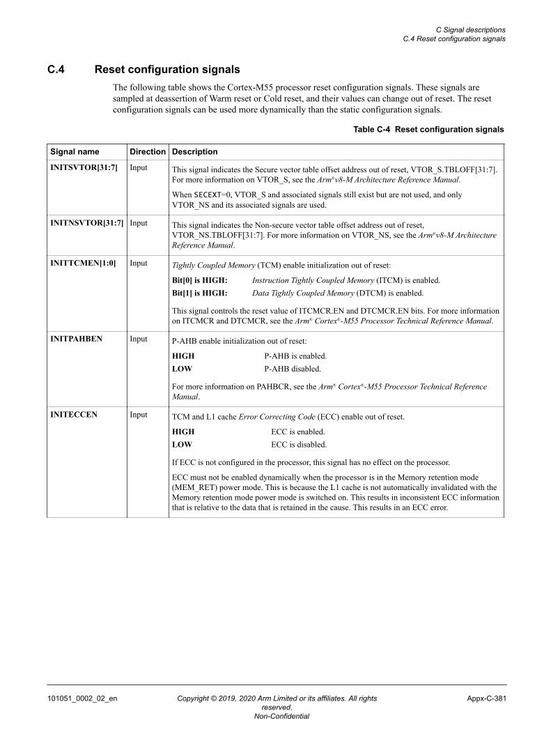
C.4 Reset configuration signalsThe following table shows the Cortex-M55 processor reset configuration signals. These signals aresampled at deassertion of Warm reset or Cold reset, and their values can change out of reset. The resetconfiguration signals can be used more dynamically than the static configuration signals.
Table C-4 Reset configuration signals
Signal name Direction Description
INITSVTOR[31:7] Input This signal indicates the Secure vector table offset address out of reset, VTOR_S.TBLOFF[31:7].For more information on VTOR_S, see the Arm®v8-M Architecture Reference Manual.
When SECEXT=0, VTOR_S and associated signals still exist but are not used, and onlyVTOR_NS and its associated signals are used.
INITNSVTOR[31:7] Input This signal indicates the Non-secure vector table offset address out of reset,VTOR_NS.TBLOFF[31:7]. For more information on VTOR_NS, see the Arm®v8-M ArchitectureReference Manual.
INITTCMEN[1:0] Input Tightly Coupled Memory (TCM) enable initialization out of reset:
Bit[0] is HIGH: Instruction Tightly Coupled Memory (ITCM) is enabled.Bit[1] is HIGH: Data Tightly Coupled Memory (DTCM) is enabled.
This signal controls the reset value of ITCMCR.EN and DTCMCR.EN bits. For more informationon ITCMCR and DTCMCR, see the Arm® Cortex®-M55 Processor Technical Reference Manual.
INITPAHBEN Input P-AHB enable initialization out of reset:
HIGH P-AHB is enabled.LOW P-AHB disabled.
For more information on PAHBCR, see the Arm® Cortex®-M55 Processor Technical ReferenceManual.
INITECCEN Input TCM and L1 cache Error Correcting Code (ECC) enable out of reset.
HIGH ECC is enabled.LOW ECC is disabled.
If ECC is not configured in the processor, this signal has no effect on the processor.
ECC must not be enabled dynamically when the processor is in the Memory retention mode(MEM_RET) power mode. This is because the L1 cache is not automatically invalidated with theMemory retention mode power mode is switched on. This results in inconsistent ECC informationthat is relative to the data that is retained in the cause. This results in an ECC error.
C Signal descriptionsC.4 Reset configuration signals
101051_0002_02_en Copyright © 2019, 2020 Arm Limited or its affiliates. All rightsreserved.
Appx-C-381
Non-Confidential
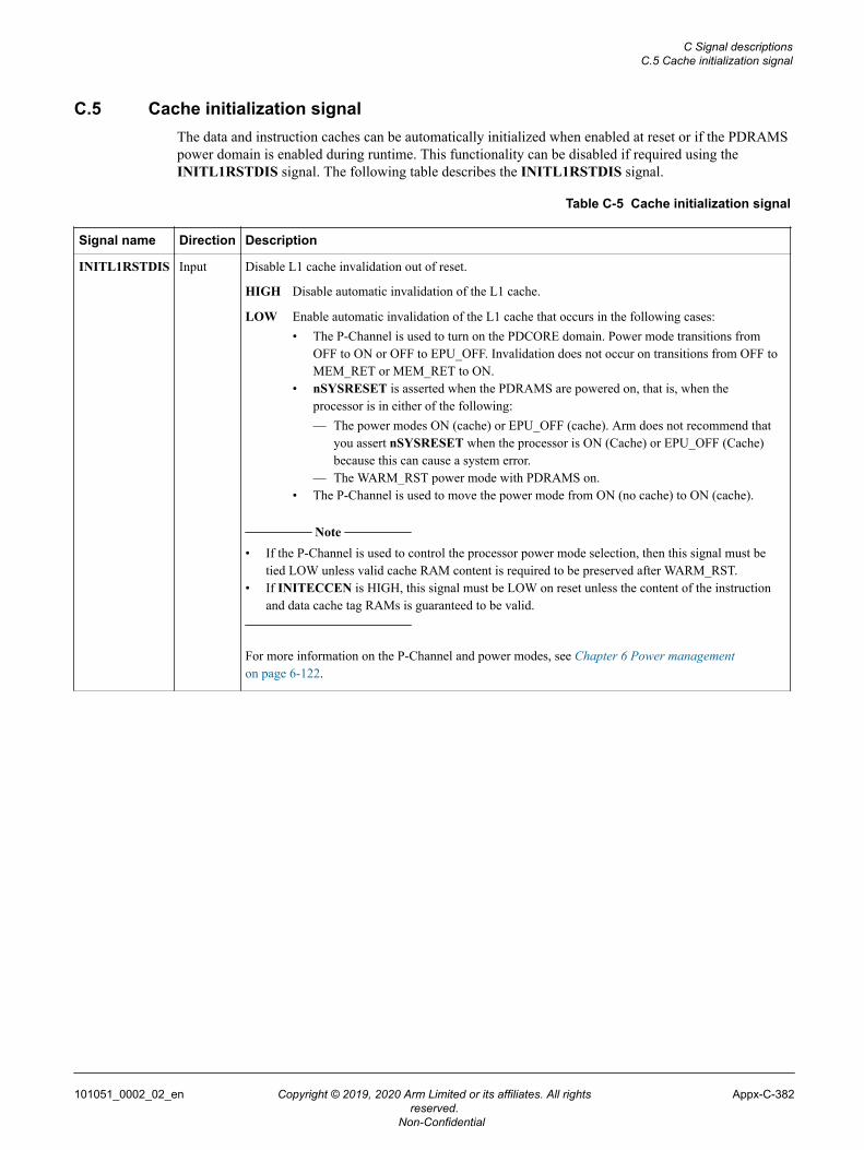
C.5 Cache initialization signalThe data and instruction caches can be automatically initialized when enabled at reset or if the PDRAMSpower domain is enabled during runtime. This functionality can be disabled if required using theINITL1RSTDIS signal. The following table describes the INITL1RSTDIS signal.
Table C-5 Cache initialization signal
Signal name Direction Description
INITL1RSTDIS Input Disable L1 cache invalidation out of reset.
HIGH Disable automatic invalidation of the L1 cache.
LOW Enable automatic invalidation of the L1 cache that occurs in the following cases:• The P-Channel is used to turn on the PDCORE domain. Power mode transitions from
OFF to ON or OFF to EPU_OFF. Invalidation does not occur on transitions from OFF toMEM_RET or MEM_RET to ON.
• nSYSRESET is asserted when the PDRAMS are powered on, that is, when theprocessor is in either of the following:— The power modes ON (cache) or EPU_OFF (cache). Arm does not recommend that
you assert nSYSRESET when the processor is ON (Cache) or EPU_OFF (Cache)because this can cause a system error.
— The WARM_RST power mode with PDRAMS on.• The P-Channel is used to move the power mode from ON (no cache) to ON (cache).
Note
• If the P-Channel is used to control the processor power mode selection, then this signal must betied LOW unless valid cache RAM content is required to be preserved after WARM_RST.
• If INITECCEN is HIGH, this signal must be LOW on reset unless the content of the instructionand data cache tag RAMs is guaranteed to be valid.
For more information on the P-Channel and power modes, see Chapter 6 Power managementon page 6-122.
C Signal descriptionsC.5 Cache initialization signal
101051_0002_02_en Copyright © 2019, 2020 Arm Limited or its affiliates. All rightsreserved.
Appx-C-382
Non-Confidential
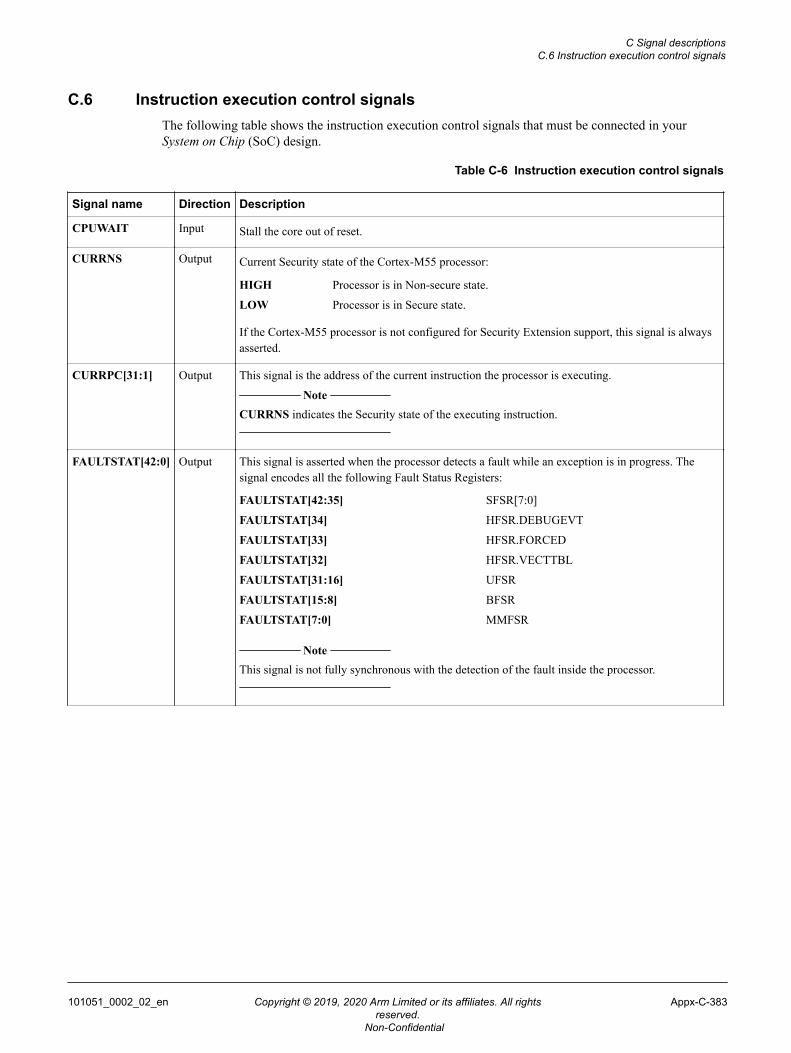
C.6 Instruction execution control signalsThe following table shows the instruction execution control signals that must be connected in yourSystem on Chip (SoC) design.
Table C-6 Instruction execution control signals
Signal name Direction Description
CPUWAIT Input Stall the core out of reset.
CURRNS Output Current Security state of the Cortex-M55 processor:
HIGH Processor is in Non-secure state.
LOW Processor is in Secure state.
If the Cortex-M55 processor is not configured for Security Extension support, this signal is alwaysasserted.
CURRPC[31:1] Output This signal is the address of the current instruction the processor is executing. Note
CURRNS indicates the Security state of the executing instruction.
FAULTSTAT[42:0] Output This signal is asserted when the processor detects a fault while an exception is in progress. Thesignal encodes all the following Fault Status Registers:
FAULTSTAT[42:35] SFSR[7:0]
FAULTSTAT[34] HFSR.DEBUGEVT
FAULTSTAT[33] HFSR.FORCED
FAULTSTAT[32] HFSR.VECTTBL
FAULTSTAT[31:16] UFSR
FAULTSTAT[15:8] BFSR
FAULTSTAT[7:0] MMFSR
Note
This signal is not fully synchronous with the detection of the fault inside the processor.
C Signal descriptionsC.6 Instruction execution control signals
101051_0002_02_en Copyright © 2019, 2020 Arm Limited or its affiliates. All rightsreserved.
Appx-C-383
Non-Confidential
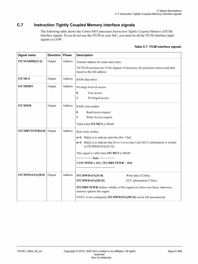
C.7 Instruction Tightly Coupled Memory interface signalsThe following table shows the Cortex-M55 processor Instruction Tightly Coupled Memory (ITCM)interface signals. If you do not use the ITCM in your SoC, you must tie all the ITCM interface inputsignals to LOW.
Table C-7 ITCM interface signals
Signal name Direction Phase Description
ITCMADDR[23:2] Output Address Transfer address for reads and writes.
All ITCM accesses are 32-bit aligned. If necessary, the processor selects read databased on the full address.
ITCMCS Output Address RAM chip select.
ITCMPRIV Output Address Privilege level of access:
0 User access.
1 Privileged access.
ITCMWR Output Address RAM write enable:
0 Read access request.
1 Write-Access request.
Valid when ITCMCS is HIGH.
ITCMBYTEWR[4:0] Output Address Byte write strobes.
n<4 Bit[n] is to indicate data bits [8n+7:8n].
n=4 Bit[n] is to indicate that Error Correcting Code (ECC) information is writtenin ITCMWDATA[38:32].
This signal is valid when ITCMCS is HIGH. Note
If ITCMWR is 0b1, ITCMBYTEWR = 0b0.
ITCMWDATA[38:0] Output Address ITCMWDATA[31:0] Write data (32-bits).
ITCMWDATA[38:32] ECC information (7-bits).
ITCMBYTEWR defines validity of this signal on a byte-wise basis, otherwise,memory ignores this signal.
If ECC is not configured, ITCMWDATA[38:32] can be left unconnected.
C Signal descriptionsC.7 Instruction Tightly Coupled Memory interface signals
101051_0002_02_en Copyright © 2019, 2020 Arm Limited or its affiliates. All rightsreserved.
Appx-C-384
Non-Confidential
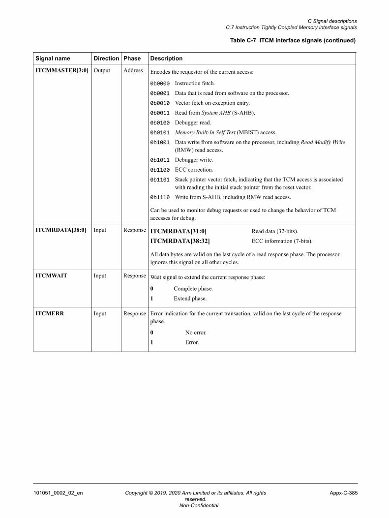
Table C-7 ITCM interface signals (continued)
Signal name Direction Phase Description
ITCMMASTER[3:0] Output Address Encodes the requestor of the current access:
0b0000 Instruction fetch.
0b0001 Data that is read from software on the processor.
0b0010 Vector fetch on exception entry.
0b0011 Read from System AHB (S-AHB).
0b0100 Debugger read.
0b0101 Memory Built-In Self Test (MBIST) access.
0b1001 Data write from software on the processor, including Read Modify Write(RMW) read access.
0b1011 Debugger write.
0b1100 ECC correction.
0b1101 Stack pointer vector fetch, indicating that the TCM access is associatedwith reading the initial stack pointer from the reset vector.
0b1110 Write from S-AHB, including RMW read access.
Can be used to monitor debug requests or used to change the behavior of TCMaccesses for debug.
ITCMRDATA[38:0] Input Response ITCMRDATA[31:0] Read data (32-bits).
ITCMRDATA[38:32] ECC information (7-bits).
All data bytes are valid on the last cycle of a read response phase. The processorignores this signal on all other cycles.
ITCMWAIT Input Response Wait signal to extend the current response phase:
0 Complete phase.
1 Extend phase.
ITCMERR Input Response Error indication for the current transaction, valid on the last cycle of the responsephase.
0 No error.
1 Error.
C Signal descriptionsC.7 Instruction Tightly Coupled Memory interface signals
101051_0002_02_en Copyright © 2019, 2020 Arm Limited or its affiliates. All rightsreserved.
Appx-C-385
Non-Confidential
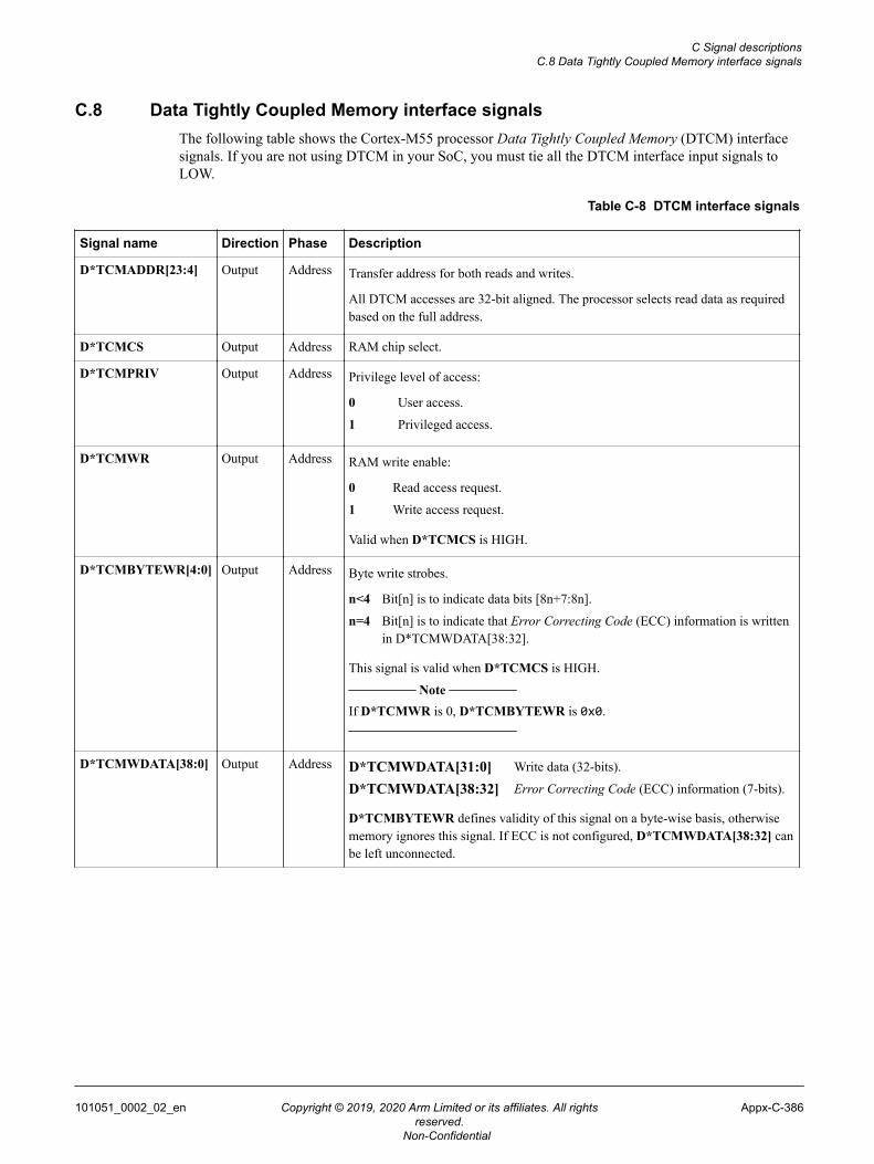
C.8 Data Tightly Coupled Memory interface signalsThe following table shows the Cortex-M55 processor Data Tightly Coupled Memory (DTCM) interfacesignals. If you are not using DTCM in your SoC, you must tie all the DTCM interface input signals toLOW.
Table C-8 DTCM interface signals
Signal name Direction Phase Description
D*TCMADDR[23:4] Output Address Transfer address for both reads and writes.
All DTCM accesses are 32-bit aligned. The processor selects read data as requiredbased on the full address.
D*TCMCS Output Address RAM chip select.
D*TCMPRIV Output Address Privilege level of access:
0 User access.
1 Privileged access.
D*TCMWR Output Address RAM write enable:
0 Read access request.
1 Write access request.
Valid when D*TCMCS is HIGH.
D*TCMBYTEWR[4:0] Output Address Byte write strobes.
n<4 Bit[n] is to indicate data bits [8n+7:8n].
n=4 Bit[n] is to indicate that Error Correcting Code (ECC) information is writtenin D*TCMWDATA[38:32].
This signal is valid when D*TCMCS is HIGH. Note
If D*TCMWR is 0, D*TCMBYTEWR is 0x0.
D*TCMWDATA[38:0] Output Address D*TCMWDATA[31:0] Write data (32-bits).
D*TCMWDATA[38:32] Error Correcting Code (ECC) information (7-bits).
D*TCMBYTEWR defines validity of this signal on a byte-wise basis, otherwisememory ignores this signal. If ECC is not configured, D*TCMWDATA[38:32] canbe left unconnected.
C Signal descriptionsC.8 Data Tightly Coupled Memory interface signals
101051_0002_02_en Copyright © 2019, 2020 Arm Limited or its affiliates. All rightsreserved.
Appx-C-386
Non-Confidential
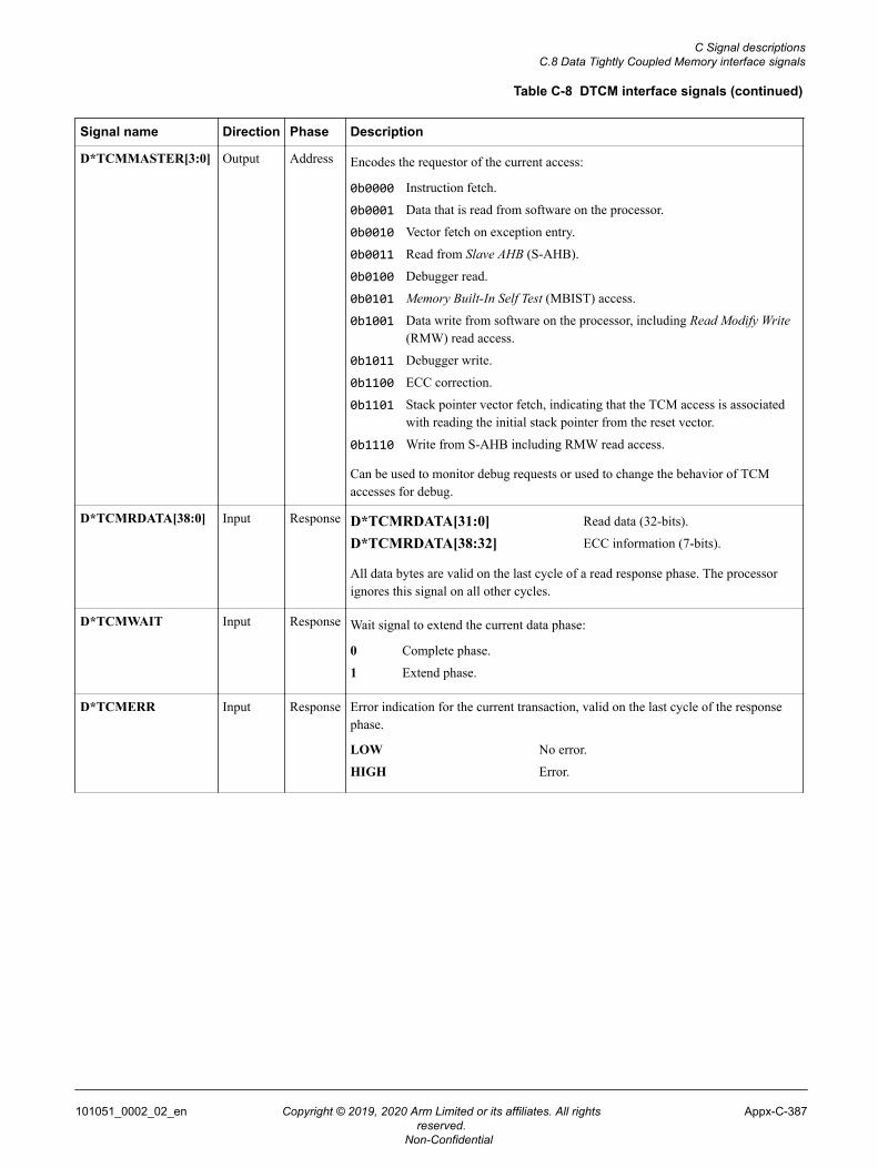
Table C-8 DTCM interface signals (continued)
Signal name Direction Phase Description
D*TCMMASTER[3:0] Output Address Encodes the requestor of the current access:
0b0000 Instruction fetch.
0b0001 Data that is read from software on the processor.
0b0010 Vector fetch on exception entry.
0b0011 Read from Slave AHB (S-AHB).
0b0100 Debugger read.
0b0101 Memory Built-In Self Test (MBIST) access.
0b1001 Data write from software on the processor, including Read Modify Write(RMW) read access.
0b1011 Debugger write.
0b1100 ECC correction.
0b1101 Stack pointer vector fetch, indicating that the TCM access is associatedwith reading the initial stack pointer from the reset vector.
0b1110 Write from S-AHB including RMW read access.
Can be used to monitor debug requests or used to change the behavior of TCMaccesses for debug.
D*TCMRDATA[38:0] Input Response D*TCMRDATA[31:0] Read data (32-bits).
D*TCMRDATA[38:32] ECC information (7-bits).
All data bytes are valid on the last cycle of a read response phase. The processorignores this signal on all other cycles.
D*TCMWAIT Input Response Wait signal to extend the current data phase:
0 Complete phase.
1 Extend phase.
D*TCMERR Input Response Error indication for the current transaction, valid on the last cycle of the responsephase.
LOW No error.
HIGH Error.
C Signal descriptionsC.8 Data Tightly Coupled Memory interface signals
101051_0002_02_en Copyright © 2019, 2020 Arm Limited or its affiliates. All rightsreserved.
Appx-C-387
Non-Confidential
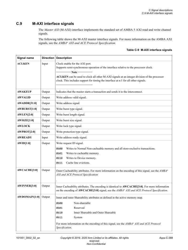
C.9 M-AXI interface signalsThe Master AXI (M-AXI) interface implements the standard set of AMBA 5 AXI read and write channelsignals.
The following table shows the M-AXI master interface signals. For more information on the AMBA AXIsignals, see the AMBA® AXI and ACE Protocol Specification.
Table C-9 M-AXI interface signals
Signal name Direction Description
ACLKEN Input Clock enable for the AXI port.Supports semi-synchronous operation of the interface relative to the processor clock.
Note
ACLKEN can be used to clock all other M-AXI signals at an integer division of the processorclock. This includes support for timing the interface at n:1 for all other signals.
AWAKEUP Output Indicates that the master starts a transaction and sends it to the interconnect.
AWVALID Output Write address valid signal.
AWADDR[31:0] Output Write address signal.
AWBURST[1:0] Output Write burst type signal.
AWLEN[2:0] Output Write burst length signal.
AWSIZE[1:0] Output Write burst size signal.
AWLOCK Output Write lock type signal.
AWPROT[2:0] Output Write protection type signal.
AWREADY Input Write address ready signal.
AWID[1:0] Output Write request ID signal.
0b00 Writes to Normal Non-cacheable memory and all store-exclusive transactions.
0b01 Writes to cacheable memory.
0b10 Writes to Device memory.
0b11 Cache line evictions.
AWCACHE[3:0] Output Outer Cacheability attributes. For more information on the encoding of this signal, see the AMBA®
AXI and ACE Protocol Specification
.
AWINNER[3:0] Output Inner Cacheability attributes. The encoding is identical to AWCACHE[3:0]. For more informationon the encoding of AWCACHE[3:0] signal, see the AMBA® AXI and ACE Protocol Specification.
AWDOMAIN[1:0] Output Inner and outer Shareability attributes as defined in the active memory map.
0b00 Non-shareable
0b01 Reserved
0b10 Inner Shareable and Outer Shareable
0b11 System
For more information on the encoding of this signal, see the AMBA® AXI and ACE ProtocolSpecification.
C Signal descriptionsC.9 M-AXI interface signals
101051_0002_02_en Copyright © 2019, 2020 Arm Limited or its affiliates. All rightsreserved.
Appx-C-388
Non-Confidential
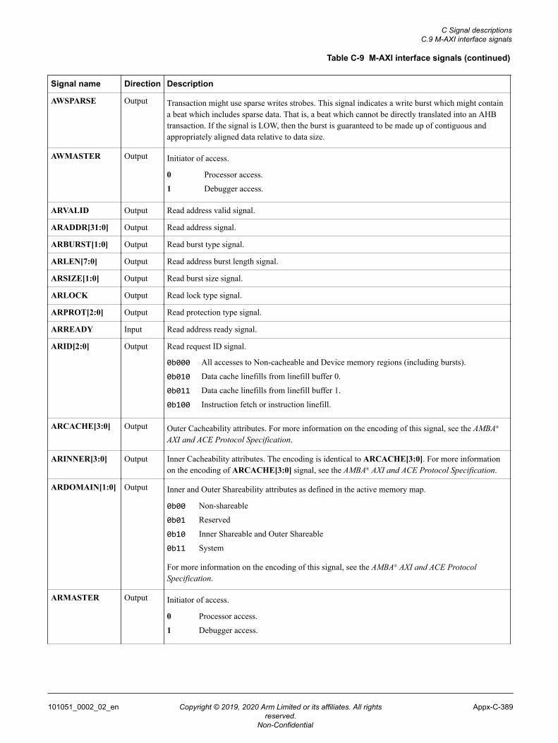
Table C-9 M-AXI interface signals (continued)
Signal name Direction Description
AWSPARSE Output Transaction might use sparse writes strobes. This signal indicates a write burst which might containa beat which includes sparse data. That is, a beat which cannot be directly translated into an AHBtransaction. If the signal is LOW, then the burst is guaranteed to be made up of contiguous andappropriately aligned data relative to data size.
AWMASTER Output Initiator of access.
0 Processor access.
1 Debugger access.
ARVALID Output Read address valid signal.
ARADDR[31:0] Output Read address signal.
ARBURST[1:0] Output Read burst type signal.
ARLEN[7:0] Output Read address burst length signal.
ARSIZE[1:0] Output Read burst size signal.
ARLOCK Output Read lock type signal.
ARPROT[2:0] Output Read protection type signal.
ARREADY Input Read address ready signal.
ARID[2:0] Output Read request ID signal.
0b000 All accesses to Non-cacheable and Device memory regions (including bursts).
0b010 Data cache linefills from linefill buffer 0.
0b011 Data cache linefills from linefill buffer 1.
0b100 Instruction fetch or instruction linefill.
ARCACHE[3:0] Output Outer Cacheability attributes. For more information on the encoding of this signal, see the AMBA®
AXI and ACE Protocol Specification.
ARINNER[3:0] Output Inner Cacheability attributes. The encoding is identical to ARCACHE[3:0]. For more informationon the encoding of ARCACHE[3:0] signal, see the AMBA® AXI and ACE Protocol Specification.
ARDOMAIN[1:0] Output Inner and Outer Shareability attributes as defined in the active memory map.
0b00 Non-shareable
0b01 Reserved
0b10 Inner Shareable and Outer Shareable
0b11 System
For more information on the encoding of this signal, see the AMBA® AXI and ACE ProtocolSpecification.
ARMASTER Output Initiator of access.
0 Processor access.
1 Debugger access.
C Signal descriptionsC.9 M-AXI interface signals
101051_0002_02_en Copyright © 2019, 2020 Arm Limited or its affiliates. All rightsreserved.
Appx-C-389
Non-Confidential
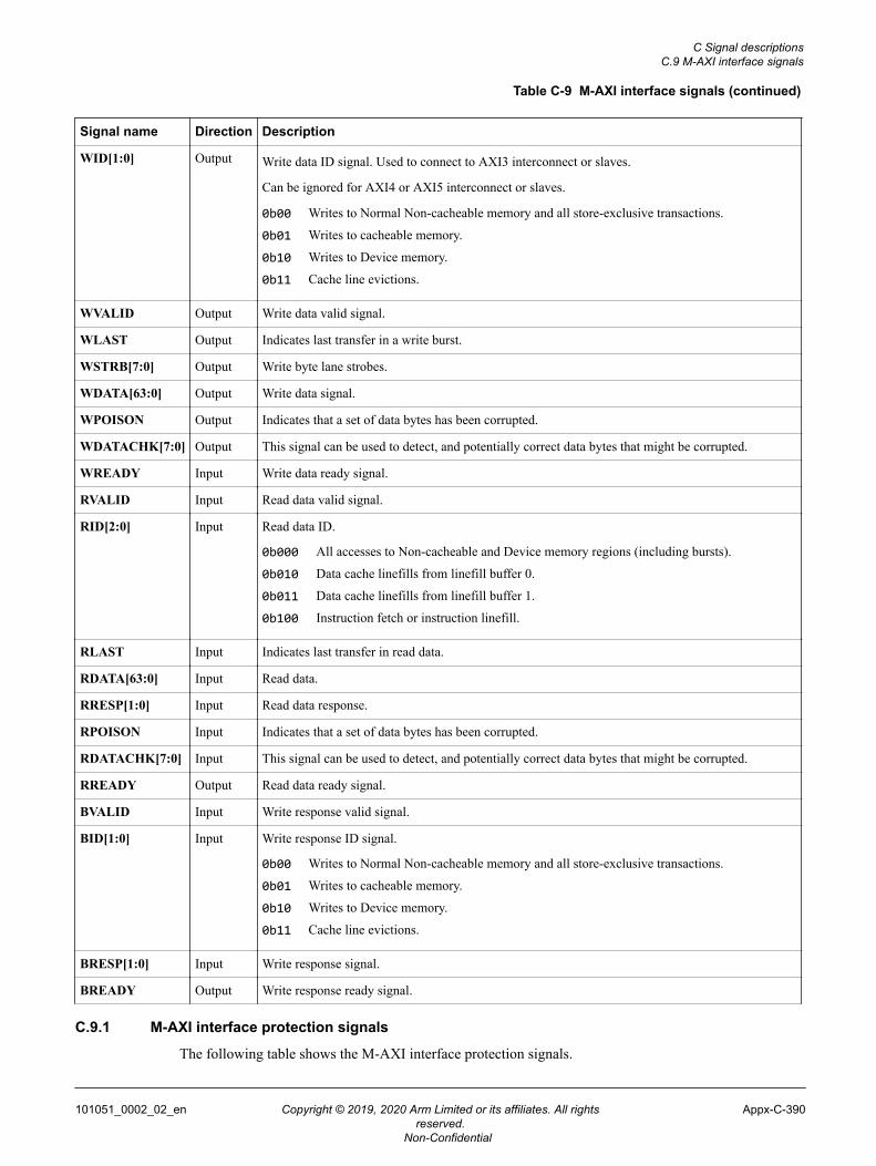
Table C-9 M-AXI interface signals (continued)
Signal name Direction Description
WID[1:0] Output Write data ID signal. Used to connect to AXI3 interconnect or slaves.
Can be ignored for AXI4 or AXI5 interconnect or slaves.
0b00 Writes to Normal Non-cacheable memory and all store-exclusive transactions.
0b01 Writes to cacheable memory.
0b10 Writes to Device memory.
0b11 Cache line evictions.
WVALID Output Write data valid signal.
WLAST Output Indicates last transfer in a write burst.
WSTRB[7:0] Output Write byte lane strobes.
WDATA[63:0] Output Write data signal.
WPOISON Output Indicates that a set of data bytes has been corrupted.
WDATACHK[7:0] Output This signal can be used to detect, and potentially correct data bytes that might be corrupted.
WREADY Input Write data ready signal.
RVALID Input Read data valid signal.
RID[2:0] Input Read data ID.
0b000 All accesses to Non-cacheable and Device memory regions (including bursts).
0b010 Data cache linefills from linefill buffer 0.
0b011 Data cache linefills from linefill buffer 1.
0b100 Instruction fetch or instruction linefill.
RLAST Input Indicates last transfer in read data.
RDATA[63:0] Input Read data.
RRESP[1:0] Input Read data response.
RPOISON Input Indicates that a set of data bytes has been corrupted.
RDATACHK[7:0] Input This signal can be used to detect, and potentially correct data bytes that might be corrupted.
RREADY Output Read data ready signal.
BVALID Input Write response valid signal.
BID[1:0] Input Write response ID signal.
0b00 Writes to Normal Non-cacheable memory and all store-exclusive transactions.
0b01 Writes to cacheable memory.
0b10 Writes to Device memory.
0b11 Cache line evictions.
BRESP[1:0] Input Write response signal.
BREADY Output Write response ready signal.
C.9.1 M-AXI interface protection signals
The following table shows the M-AXI interface protection signals.
C Signal descriptionsC.9 M-AXI interface signals
101051_0002_02_en Copyright © 2019, 2020 Arm Limited or its affiliates. All rightsreserved.
Appx-C-390
Non-Confidential
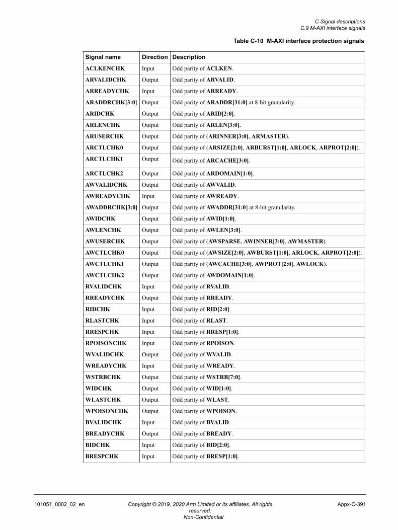
Table C-10 M-AXI interface protection signals
Signal name Direction Description
ACLKENCHK Input Odd parity of ACLKEN.
ARVALIDCHK Output Odd parity of ARVALID.
ARREADYCHK Input Odd parity of ARREADY.
ARADDRCHK[3:0] Output Odd parity of ARADDR[31:0] at 8-bit granularity.
ARIDCHK Output Odd parity of ARID[2:0].
ARLENCHK Output Odd parity of ARLEN[3:0].
ARUSERCHK Output Odd parity of (ARINNER[3:0], ARMASTER).
ARCTLCHK0 Output Odd parity of (ARSIZE[2:0], ARBURST[1:0], ARLOCK, ARPROT[2:0]).
ARCTLCHK1 Output Odd parity of ARCACHE[3:0].
ARCTLCHK2 Output Odd parity of ARDOMAIN[1:0].
AWVALIDCHK Output Odd parity of AWVALID.
AWREADYCHK Input Odd parity of AWREADY.
AWADDRCHK[3:0] Output Odd parity of AWADDR[31:0] at 8-bit granularity.
AWIDCHK Output Odd parity of AWID[1:0].
AWLENCHK Output Odd parity of AWLEN[3:0].
AWUSERCHK Output Odd parity of (AWSPARSE, AWINNER[3:0], AWMASTER).
AWCTLCHK0 Output Odd parity of (AWSIZE[2:0], AWBURST[1:0], ARLOCK, ARPROT[2:0]).
AWCTLCHK1 Output Odd parity of (AWCACHE[3:0], AWPROT[2:0], AWLOCK).
AWCTLCHK2 Output Odd parity of AWDOMAIN[1:0].
RVALIDCHK Input Odd parity of RVALID.
RREADYCHK Output Odd parity of RREADY.
RIDCHK Input Odd parity of RID[2:0].
RLASTCHK Input Odd parity of RLAST.
RRESPCHK Input Odd parity of RRESP[1:0].
RPOISONCHK Input Odd parity of RPOISON.
WVALIDCHK Output Odd parity of WVALID.
WREADYCHK Input Odd parity of WREADY.
WSTRBCHK Output Odd parity of WSTRB[7:0].
WIDCHK Output Odd parity of WID[1:0].
WLASTCHK Output Odd parity of WLAST.
WPOISONCHK Output Odd parity of WPOISON.
BVALIDCHK Input Odd parity of BVALID.
BREADYCHK Output Odd parity of BREADY.
BIDCHK Input Odd parity of BID[2:0].
BRESPCHK Input Odd parity of BRESP[1:0].
C Signal descriptionsC.9 M-AXI interface signals
101051_0002_02_en Copyright © 2019, 2020 Arm Limited or its affiliates. All rightsreserved.
Appx-C-391
Non-Confidential
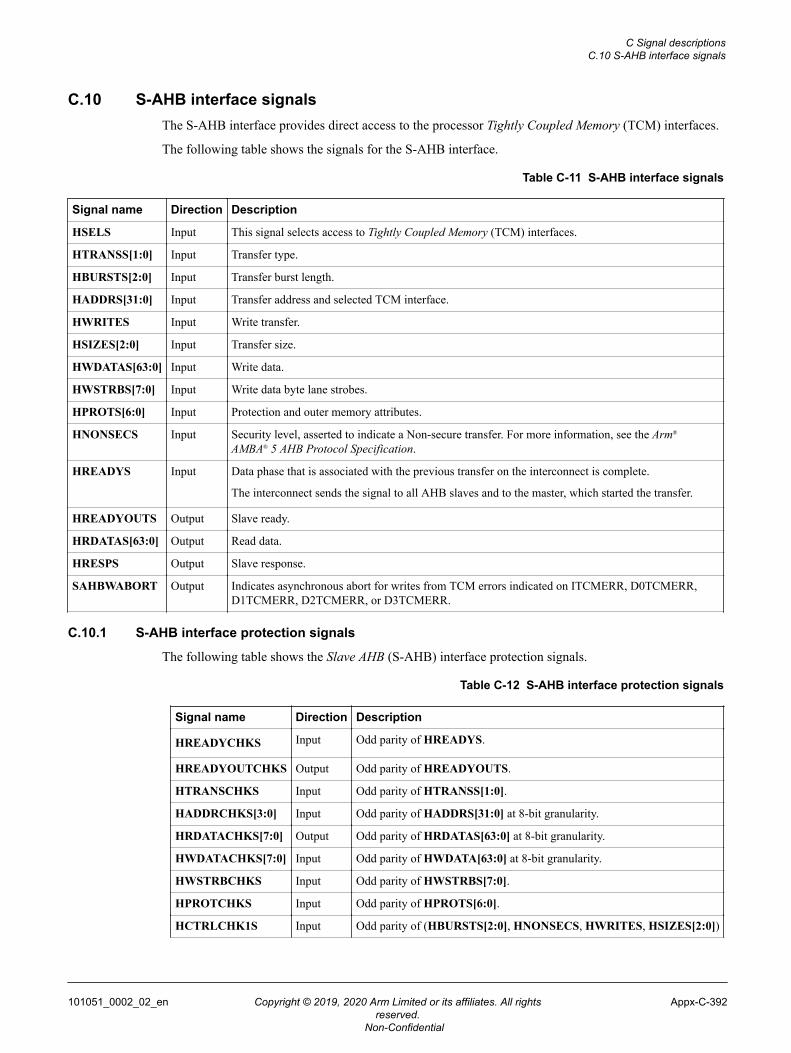
C.10 S-AHB interface signalsThe S-AHB interface provides direct access to the processor Tightly Coupled Memory (TCM) interfaces.
The following table shows the signals for the S-AHB interface.
Table C-11 S-AHB interface signals
Signal name Direction Description
HSELS Input This signal selects access to Tightly Coupled Memory (TCM) interfaces.
HTRANSS[1:0] Input Transfer type.
HBURSTS[2:0] Input Transfer burst length.
HADDRS[31:0] Input Transfer address and selected TCM interface.
HWRITES Input Write transfer.
HSIZES[2:0] Input Transfer size.
HWDATAS[63:0] Input Write data.
HWSTRBS[7:0] Input Write data byte lane strobes.
HPROTS[6:0] Input Protection and outer memory attributes.
HNONSECS Input Security level, asserted to indicate a Non-secure transfer. For more information, see the Arm®
AMBA® 5 AHB Protocol Specification.
HREADYS Input Data phase that is associated with the previous transfer on the interconnect is complete.
The interconnect sends the signal to all AHB slaves and to the master, which started the transfer.
HREADYOUTS Output Slave ready.
HRDATAS[63:0] Output Read data.
HRESPS Output Slave response.
SAHBWABORT Output Indicates asynchronous abort for writes from TCM errors indicated on ITCMERR, D0TCMERR,D1TCMERR, D2TCMERR, or D3TCMERR.
C.10.1 S-AHB interface protection signals
The following table shows the Slave AHB (S-AHB) interface protection signals.
Table C-12 S-AHB interface protection signals
Signal name Direction Description
HREADYCHKS Input Odd parity of HREADYS.
HREADYOUTCHKS Output Odd parity of HREADYOUTS.
HTRANSCHKS Input Odd parity of HTRANSS[1:0].
HADDRCHKS[3:0] Input Odd parity of HADDRS[31:0] at 8-bit granularity.
HRDATACHKS[7:0] Output Odd parity of HRDATAS[63:0] at 8-bit granularity.
HWDATACHKS[7:0] Input Odd parity of HWDATA[63:0] at 8-bit granularity.
HWSTRBCHKS Input Odd parity of HWSTRBS[7:0].
HPROTCHKS Input Odd parity of HPROTS[6:0].
HCTRLCHK1S Input Odd parity of (HBURSTS[2:0], HNONSECS, HWRITES, HSIZES[2:0])
C Signal descriptionsC.10 S-AHB interface signals
101051_0002_02_en Copyright © 2019, 2020 Arm Limited or its affiliates. All rightsreserved.
Appx-C-392
Non-Confidential

Table C-12 S-AHB interface protection signals (continued)
Signal name Direction Description
HRESPCHKS Output Odd parity of HRESPS.
HSELCHKS Input Odd parity of HSELS.
C Signal descriptionsC.10 S-AHB interface signals
101051_0002_02_en Copyright © 2019, 2020 Arm Limited or its affiliates. All rightsreserved.
Appx-C-393
Non-Confidential
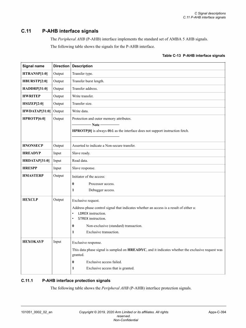
C.11 P-AHB interface signalsThe Peripheral AHB (P-AHB) interface implements the standard set of AMBA 5 AHB signals.
The following table shows the signals for the P-AHB interface.
Table C-13 P-AHB interface signals
Signal name Direction Description
HTRANSP[1:0] Output Transfer type.
HBURSTP[2:0] Output Transfer burst length.
HADDRP[31:0] Output Transfer address.
HWRITEP Output Write transfer.
HSIZEP[2:0] Output Transfer size.
HWDATAP[31:0] Output Write data.
HPROTP[6:0] Output Protection and outer memory attributes. Note
HPROTP[0] is always 0b1 as the interface does not support instruction fetch.
HNONSECP Output Asserted to indicate a Non-secure transfer.
HREADYP Input Slave ready.
HRDATAP[31:0] Input Read data.
HRESPP Input Slave response.
HMASTERP Output Initiator of the access:
0 Processor access.
1 Debugger access.
HEXCLP Output Exclusive request.
Address phase control signal that indicates whether an access is a result of either a:• LDREX instruction.• STREX instruction.
0 Non-exclusive (standard) transaction.
1 Exclusive transaction.
HEXOKAYP Input Exclusive response.
This data phase signal is sampled on HREADYC, and it indicates whether the exclusive request wasgranted.
0 Exclusive access failed.
1 Exclusive access that is granted.
C.11.1 P-AHB interface protection signals
The following table shows the Peripheral AHB (P-AHB) interface protection signals.
C Signal descriptionsC.11 P-AHB interface signals
101051_0002_02_en Copyright © 2019, 2020 Arm Limited or its affiliates. All rightsreserved.
Appx-C-394
Non-Confidential
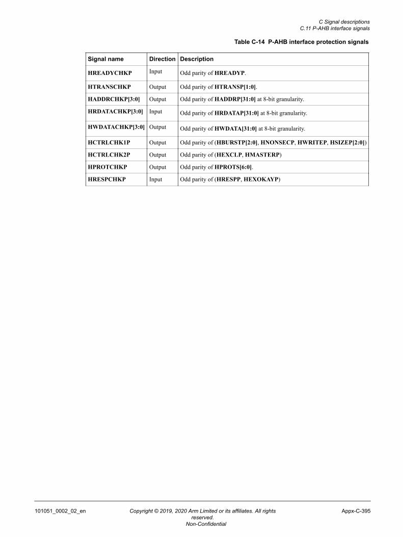
Table C-14 P-AHB interface protection signals
Signal name Direction Description
HREADYCHKP Input Odd parity of HREADYP.
HTRANSCHKP Output Odd parity of HTRANSP[1:0].
HADDRCHKP[3:0] Output Odd parity of HADDRP[31:0] at 8-bit granularity.
HRDATACHKP[3:0] Input Odd parity of HRDATAP[31:0] at 8-bit granularity.
HWDATACHKP[3:0] Output Odd parity of HWDATA[31:0] at 8-bit granularity.
HCTRLCHK1P Output Odd parity of (HBURSTP[2:0], HNONSECP, HWRITEP, HSIZEP[2:0])
HCTRLCHK2P Output Odd parity of (HEXCLP, HMASTERP)
HPROTCHKP Output Odd parity of HPROTS[6:0].
HRESPCHKP Input Odd parity of (HRESPP, HEXOKAYP)
C Signal descriptionsC.11 P-AHB interface signals
101051_0002_02_en Copyright © 2019, 2020 Arm Limited or its affiliates. All rightsreserved.
Appx-C-395
Non-Confidential
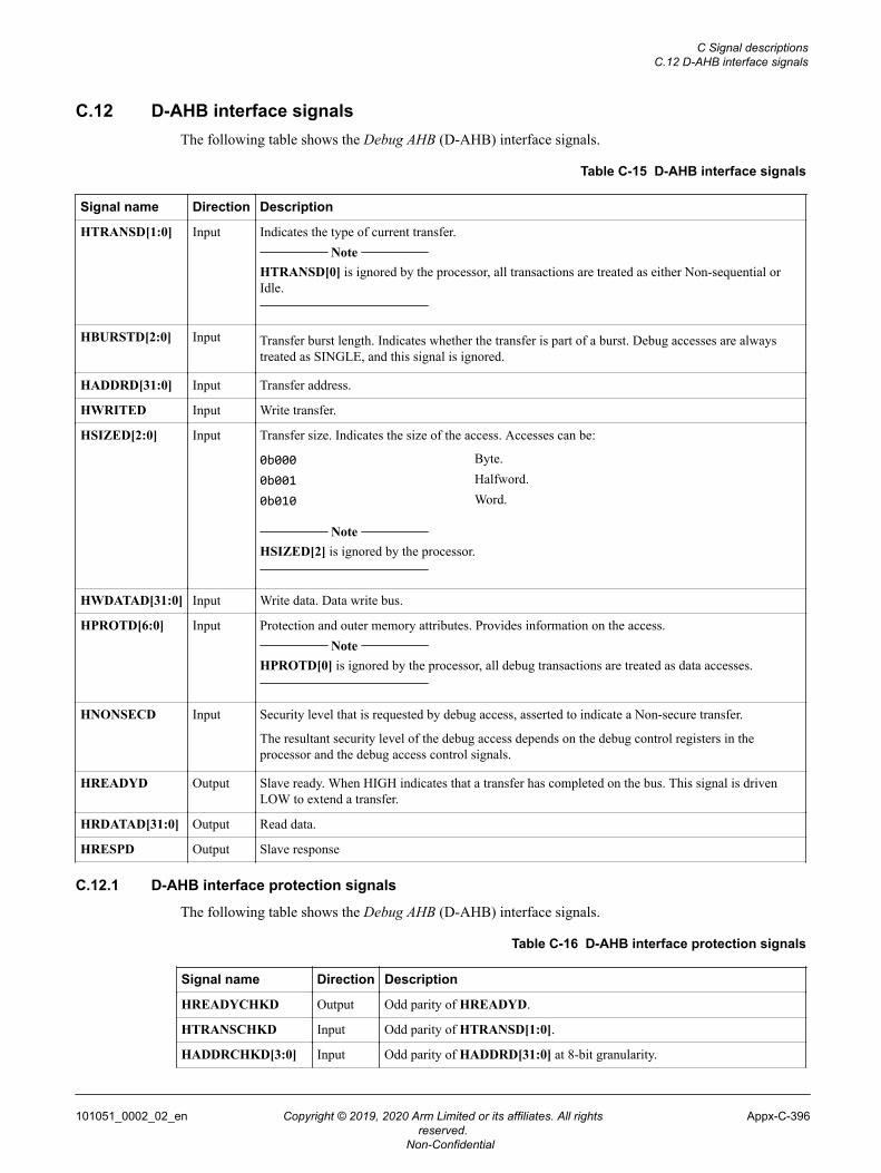
C.12 D-AHB interface signalsThe following table shows the Debug AHB (D-AHB) interface signals.
Table C-15 D-AHB interface signals
Signal name Direction Description
HTRANSD[1:0] Input Indicates the type of current transfer. Note
HTRANSD[0] is ignored by the processor, all transactions are treated as either Non-sequential orIdle.
HBURSTD[2:0] Input Transfer burst length. Indicates whether the transfer is part of a burst. Debug accesses are alwaystreated as SINGLE, and this signal is ignored.
HADDRD[31:0] Input Transfer address.
HWRITED Input Write transfer.
HSIZED[2:0] Input Transfer size. Indicates the size of the access. Accesses can be:
0b000 Byte.0b001 Halfword.0b010 Word.
Note
HSIZED[2] is ignored by the processor.
HWDATAD[31:0] Input Write data. Data write bus.
HPROTD[6:0] Input Protection and outer memory attributes. Provides information on the access. Note
HPROTD[0] is ignored by the processor, all debug transactions are treated as data accesses.
HNONSECD Input Security level that is requested by debug access, asserted to indicate a Non-secure transfer.
The resultant security level of the debug access depends on the debug control registers in theprocessor and the debug access control signals.
HREADYD Output Slave ready. When HIGH indicates that a transfer has completed on the bus. This signal is drivenLOW to extend a transfer.
HRDATAD[31:0] Output Read data.
HRESPD Output Slave response
C.12.1 D-AHB interface protection signals
The following table shows the Debug AHB (D-AHB) interface signals.
Table C-16 D-AHB interface protection signals
Signal name Direction Description
HREADYCHKD Output Odd parity of HREADYD.
HTRANSCHKD Input Odd parity of HTRANSD[1:0].
HADDRCHKD[3:0] Input Odd parity of HADDRD[31:0] at 8-bit granularity.
C Signal descriptionsC.12 D-AHB interface signals
101051_0002_02_en Copyright © 2019, 2020 Arm Limited or its affiliates. All rightsreserved.
Appx-C-396
Non-Confidential

Table C-16 D-AHB interface protection signals (continued)
Signal name Direction Description
HRDATACHKD[3:0] Output Odd parity of HRDATAD[31:0] at 8-bit granularity.
HWDATACHKD[3:0] Input Odd parity of HWDATAD[31:0] at 8-bit granularity.
HCTRLCHK1D Input Odd parity of (HBURSTD[2:0], HNONSECD, HWRITED, HSIZED[2:0]).
HPROTCHKD Input Odd parity of HPROTD[6:0].
HRESPCHKD Output Odd parity of HRESPD.
C Signal descriptionsC.12 D-AHB interface signals
101051_0002_02_en Copyright © 2019, 2020 Arm Limited or its affiliates. All rightsreserved.
Appx-C-397
Non-Confidential
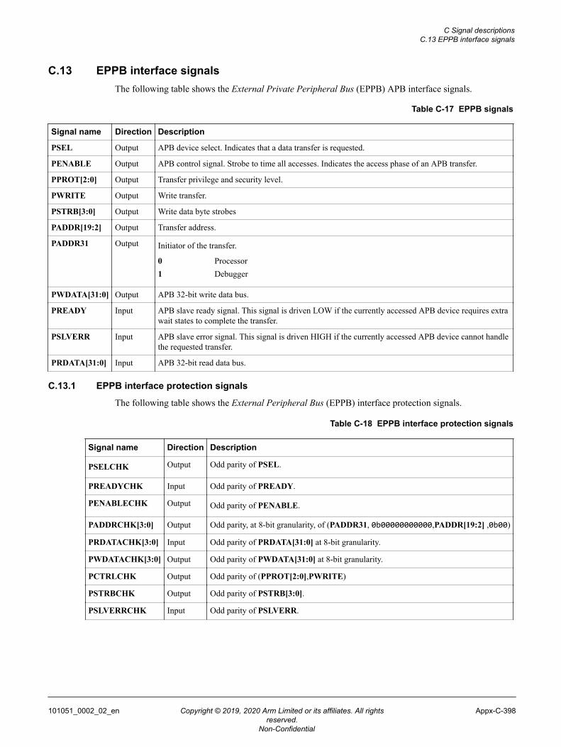
C.13 EPPB interface signalsThe following table shows the External Private Peripheral Bus (EPPB) APB interface signals.
Table C-17 EPPB signals
Signal name Direction Description
PSEL Output APB device select. Indicates that a data transfer is requested.
PENABLE Output APB control signal. Strobe to time all accesses. Indicates the access phase of an APB transfer.
PPROT[2:0] Output Transfer privilege and security level.
PWRITE Output Write transfer.
PSTRB[3:0] Output Write data byte strobes
PADDR[19:2] Output Transfer address.
PADDR31 Output Initiator of the transfer.
0 Processor1 Debugger
PWDATA[31:0] Output APB 32-bit write data bus.
PREADY Input APB slave ready signal. This signal is driven LOW if the currently accessed APB device requires extrawait states to complete the transfer.
PSLVERR Input APB slave error signal. This signal is driven HIGH if the currently accessed APB device cannot handlethe requested transfer.
PRDATA[31:0] Input APB 32-bit read data bus.
C.13.1 EPPB interface protection signals
The following table shows the External Peripheral Bus (EPPB) interface protection signals.
Table C-18 EPPB interface protection signals
Signal name Direction Description
PSELCHK Output Odd parity of PSEL.
PREADYCHK Input Odd parity of PREADY.
PENABLECHK Output Odd parity of PENABLE.
PADDRCHK[3:0] Output Odd parity, at 8-bit granularity, of (PADDR31, 0b00000000000,PADDR[19:2] ,0b00)
PRDATACHK[3:0] Input Odd parity of PRDATA[31:0] at 8-bit granularity.
PWDATACHK[3:0] Output Odd parity of PWDATA[31:0] at 8-bit granularity.
PCTRLCHK Output Odd parity of (PPROT[2:0],PWRITE)
PSTRBCHK Output Odd parity of PSTRB[3:0].
PSLVERRCHK Input Odd parity of PSLVERR.
C Signal descriptionsC.13 EPPB interface signals
101051_0002_02_en Copyright © 2019, 2020 Arm Limited or its affiliates. All rightsreserved.
Appx-C-398
Non-Confidential
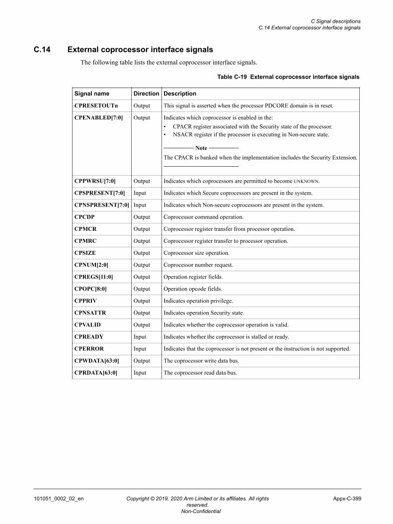
C.14 External coprocessor interface signalsThe following table lists the external coprocessor interface signals.
Table C-19 External coprocessor interface signals
Signal name Direction Description
CPRESETOUTn Output This signal is asserted when the processor PDCORE domain is in reset.
CPENABLED[7:0] Output Indicates which coprocessor is enabled in the:• CPACR register associated with the Security state of the processor.• NSACR register if the processor is executing in Non-secure state.
Note
The CPACR is banked when the implementation includes the Security Extension.
CPPWRSU[7:0] Output Indicates which coprocessors are permitted to become UNKNOWN.
CPSPRESENT[7:0] Input Indicates which Secure coprocessors are present in the system.
CPNSPRESENT[7:0] Input Indicates which Non-secure coprocessors are present in the system.
CPCDP Output Coprocessor command operation.
CPMCR Output Coprocessor register transfer from processor operation.
CPMRC Output Coprocessor register transfer to processor operation.
CPSIZE Output Coprocessor size operation.
CPNUM[2:0] Output Coprocessor number request.
CPREGS[11:0] Output Operation register fields.
CPOPC[8:0] Output Operation opcode fields.
CPPRIV Output Indicates operation privilege.
CPNSATTR Output Indicates operation Security state.
CPVALID Output Indicates whether the coprocessor operation is valid.
CPREADY Input Indicates whether the coprocessor is stalled or ready.
CPERROR Input Indicates that the coprocessor is not present or the instruction is not supported.
CPWDATA[63:0] Output The coprocessor write data bus.
CPRDATA[63:0] Input The coprocessor read data bus.
C Signal descriptionsC.14 External coprocessor interface signals
101051_0002_02_en Copyright © 2019, 2020 Arm Limited or its affiliates. All rightsreserved.
Appx-C-399
Non-Confidential
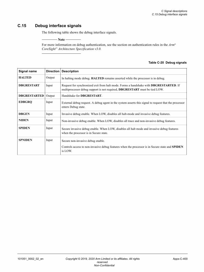
C.15 Debug interface signalsThe following table shows the debug interface signals.
Note
For more information on debug authentication, see the section on authentication rules in the Arm®
CoreSight™ Architecture Specification v3.0.
Table C-20 Debug signals
Signal name Direction Description
HALTED Output In halting mode debug. HALTED remains asserted while the processor is in debug.
DBGRESTART Input Request for synchronized exit from halt mode. Forms a handshake with DBGRESTARTED. Ifmultiprocessor debug support is not required, DBGRESTART must be tied LOW.
DBGRESTARTED Output Handshake for DBGRESTART.
EDBGRQ Input External debug request. A debug agent in the system asserts this signal to request that the processorenters Debug state.
DBGEN Input Invasive debug enable. When LOW, disables all halt-mode and invasive debug features.
NIDEN Input Non-invasive debug enable. When LOW, disables all trace and non-invasive debug features.
SPIDEN Input Secure invasive debug enable. When LOW, disables all halt mode and invasive debug featureswhen the processor is in Secure state.
SPNIDEN Input Secure non-invasive debug enable.
Controls access to non-invasive debug features when the processor is in Secure state and SPIDENis LOW.
C Signal descriptionsC.15 Debug interface signals
101051_0002_02_en Copyright © 2019, 2020 Arm Limited or its affiliates. All rightsreserved.
Appx-C-400
Non-Confidential
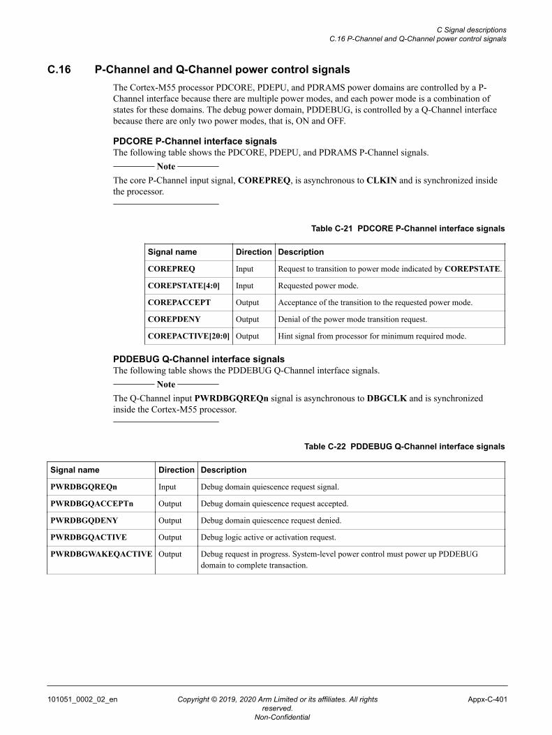
C.16 P-Channel and Q-Channel power control signalsThe Cortex-M55 processor PDCORE, PDEPU, and PDRAMS power domains are controlled by a P-Channel interface because there are multiple power modes, and each power mode is a combination ofstates for these domains. The debug power domain, PDDEBUG, is controlled by a Q-Channel interfacebecause there are only two power modes, that is, ON and OFF.
PDCORE P-Channel interface signalsThe following table shows the PDCORE, PDEPU, and PDRAMS P-Channel signals.
Note
The core P-Channel input signal, COREPREQ, is asynchronous to CLKIN and is synchronized insidethe processor.
Table C-21 PDCORE P-Channel interface signals
Signal name Direction Description
COREPREQ Input Request to transition to power mode indicated by COREPSTATE.
COREPSTATE[4:0] Input Requested power mode.
COREPACCEPT Output Acceptance of the transition to the requested power mode.
COREPDENY Output Denial of the power mode transition request.
COREPACTIVE[20:0] Output Hint signal from processor for minimum required mode.
PDDEBUG Q-Channel interface signalsThe following table shows the PDDEBUG Q-Channel interface signals.
Note
The Q-Channel input PWRDBGQREQn signal is asynchronous to DBGCLK and is synchronizedinside the Cortex-M55 processor.
Table C-22 PDDEBUG Q-Channel interface signals
Signal name Direction Description
PWRDBGQREQn Input Debug domain quiescence request signal.
PWRDBGQACCEPTn Output Debug domain quiescence request accepted.
PWRDBGQDENY Output Debug domain quiescence request denied.
PWRDBGQACTIVE Output Debug logic active or activation request.
PWRDBGWAKEQACTIVE Output Debug request in progress. System-level power control must power up PDDEBUGdomain to complete transaction.
C Signal descriptionsC.16 P-Channel and Q-Channel power control signals
101051_0002_02_en Copyright © 2019, 2020 Arm Limited or its affiliates. All rightsreserved.
Appx-C-401
Non-Confidential
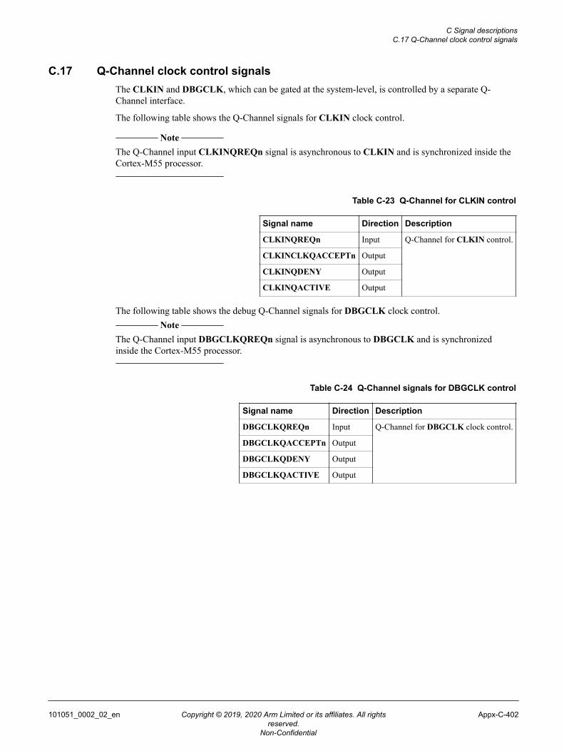
C.17 Q-Channel clock control signalsThe CLKIN and DBGCLK, which can be gated at the system-level, is controlled by a separate Q-Channel interface.
The following table shows the Q-Channel signals for CLKIN clock control.
Note
The Q-Channel input CLKINQREQn signal is asynchronous to CLKIN and is synchronized inside theCortex-M55 processor.
Table C-23 Q-Channel for CLKIN control
Signal name Direction Description
CLKINQREQn Input Q-Channel for CLKIN control.
CLKINCLKQACCEPTn Output
CLKINQDENY Output
CLKINQACTIVE Output
The following table shows the debug Q-Channel signals for DBGCLK clock control. Note
The Q-Channel input DBGCLKQREQn signal is asynchronous to DBGCLK and is synchronizedinside the Cortex-M55 processor.
Table C-24 Q-Channel signals for DBGCLK control
Signal name Direction Description
DBGCLKQREQn Input Q-Channel for DBGCLK clock control.
DBGCLKQACCEPTn Output
DBGCLKQDENY Output
DBGCLKQACTIVE Output
C Signal descriptionsC.17 Q-Channel clock control signals
101051_0002_02_en Copyright © 2019, 2020 Arm Limited or its affiliates. All rightsreserved.
Appx-C-402
Non-Confidential
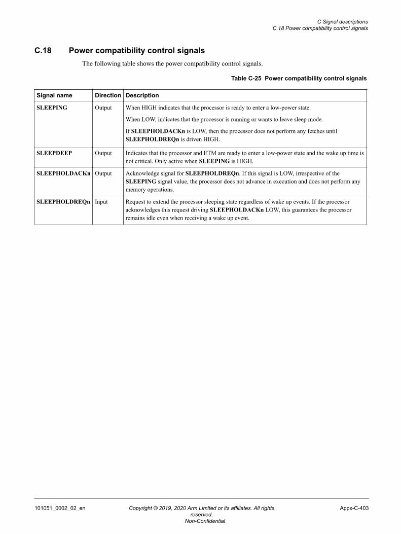
C.18 Power compatibility control signalsThe following table shows the power compatibility control signals.
Table C-25 Power compatibility control signals
Signal name Direction Description
SLEEPING Output When HIGH indicates that the processor is ready to enter a low-power state.
When LOW, indicates that the processor is running or wants to leave sleep mode.
If SLEEPHOLDACKn is LOW, then the processor does not perform any fetches untilSLEEPHOLDREQn is driven HIGH.
SLEEPDEEP Output Indicates that the processor and ETM are ready to enter a low-power state and the wake up time isnot critical. Only active when SLEEPING is HIGH.
SLEEPHOLDACKn Output Acknowledge signal for SLEEPHOLDREQn. If this signal is LOW, irrespective of theSLEEPING signal value, the processor does not advance in execution and does not perform anymemory operations.
SLEEPHOLDREQn Input Request to extend the processor sleeping state regardless of wake up events. If the processoracknowledges this request driving SLEEPHOLDACKn LOW, this guarantees the processorremains idle even when receiving a wake up event.
C Signal descriptionsC.18 Power compatibility control signals
101051_0002_02_en Copyright © 2019, 2020 Arm Limited or its affiliates. All rightsreserved.
Appx-C-403
Non-Confidential
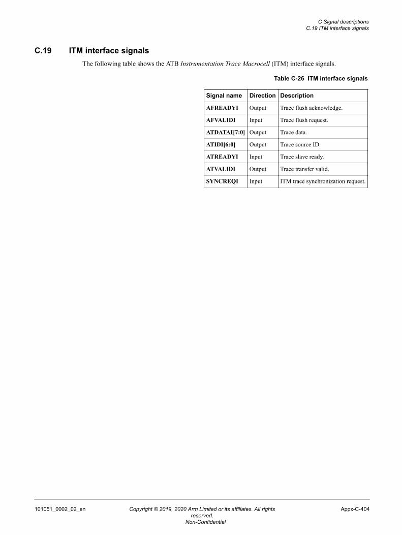
C.19 ITM interface signalsThe following table shows the ATB Instrumentation Trace Macrocell (ITM) interface signals.
Table C-26 ITM interface signals
Signal name Direction Description
AFREADYI Output Trace flush acknowledge.
AFVALIDI Input Trace flush request.
ATDATAI[7:0] Output Trace data.
ATIDI[6:0] Output Trace source ID.
ATREADYI Input Trace slave ready.
ATVALIDI Output Trace transfer valid.
SYNCREQI Input ITM trace synchronization request.
C Signal descriptionsC.19 ITM interface signals
101051_0002_02_en Copyright © 2019, 2020 Arm Limited or its affiliates. All rightsreserved.
Appx-C-404
Non-Confidential
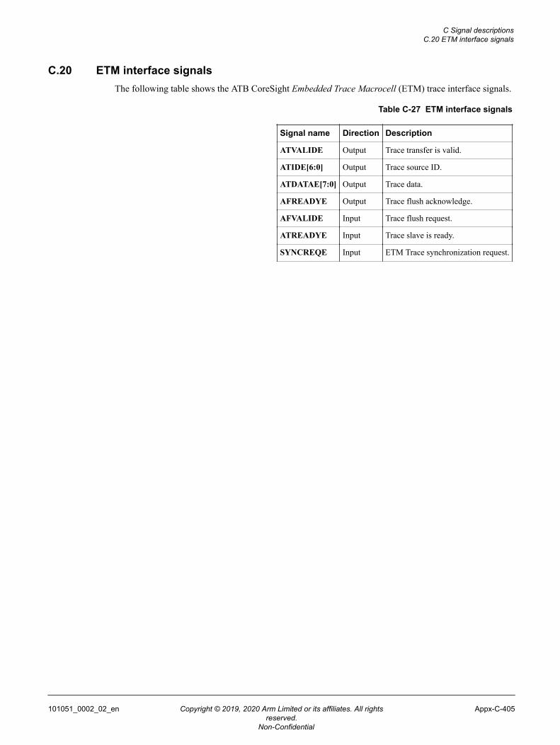
C.20 ETM interface signalsThe following table shows the ATB CoreSight Embedded Trace Macrocell (ETM) trace interface signals.
Table C-27 ETM interface signals
Signal name Direction Description
ATVALIDE Output Trace transfer is valid.
ATIDE[6:0] Output Trace source ID.
ATDATAE[7:0] Output Trace data.
AFREADYE Output Trace flush acknowledge.
AFVALIDE Input Trace flush request.
ATREADYE Input Trace slave is ready.
SYNCREQE Input ETM Trace synchronization request.
C Signal descriptionsC.20 ETM interface signals
101051_0002_02_en Copyright © 2019, 2020 Arm Limited or its affiliates. All rightsreserved.
Appx-C-405
Non-Confidential
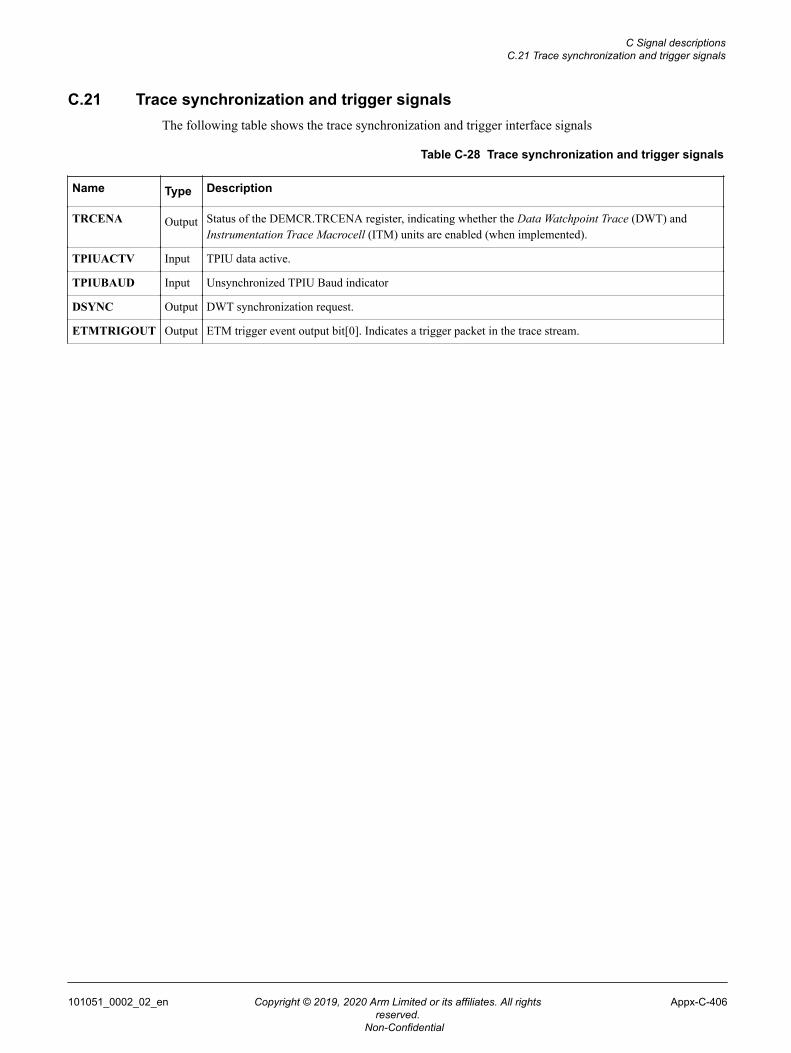
C.21 Trace synchronization and trigger signalsThe following table shows the trace synchronization and trigger interface signals
Table C-28 Trace synchronization and trigger signals
Name Type Description
TRCENA Output Status of the DEMCR.TRCENA register, indicating whether the Data Watchpoint Trace (DWT) andInstrumentation Trace Macrocell (ITM) units are enabled (when implemented).
TPIUACTV Input TPIU data active.
TPIUBAUD Input Unsynchronized TPIU Baud indicator
DSYNC Output DWT synchronization request.
ETMTRIGOUT Output ETM trigger event output bit[0]. Indicates a trigger packet in the trace stream.
C Signal descriptionsC.21 Trace synchronization and trigger signals
101051_0002_02_en Copyright © 2019, 2020 Arm Limited or its affiliates. All rightsreserved.
Appx-C-406
Non-Confidential
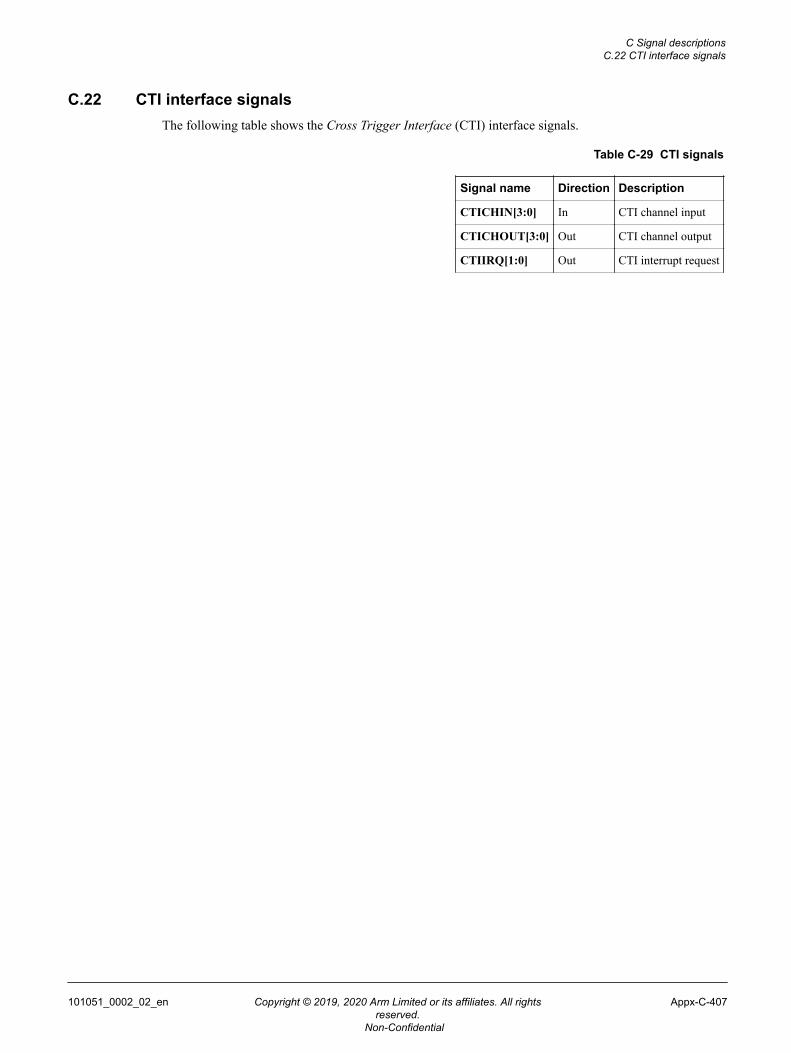
C.22 CTI interface signalsThe following table shows the Cross Trigger Interface (CTI) interface signals.
Table C-29 CTI signals
Signal name Direction Description
CTICHIN[3:0] In CTI channel input
CTICHOUT[3:0] Out CTI channel output
CTIIRQ[1:0] Out CTI interrupt request
C Signal descriptionsC.22 CTI interface signals
101051_0002_02_en Copyright © 2019, 2020 Arm Limited or its affiliates. All rightsreserved.
Appx-C-407
Non-Confidential
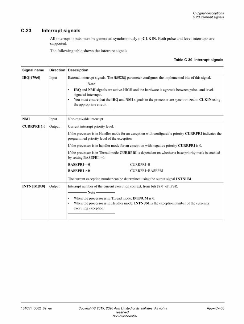
C.23 Interrupt signalsAll interrupt inputs must be generated synchronously to CLKIN. Both pulse and level interrupts aresupported.
The following table shows the interrupt signals
Table C-30 Interrupt signals
Signal name Direction Description
IRQ[479:0] Input External interrupt signals. The NUMIRQ parameter configures the implemented bits of this signal. Note
• IRQ and NMI signals are active-HIGH and the hardware is agnostic between pulse- and level-signaled interrupts.
• You must ensure that the IRQ and NMI signals to the processor are synchronized to CLKIN usingthe appropriate circuit.
NMI Input Non-maskable interrupt
CURRPRI[7:0] Output Current interrupt priority level.
If the processor is in Handler mode for an exception with configurable priority CURRPRI indicates theprogrammed priority level of the exception.
If the processor is in handler mode for an exception with negative priority CURRPRI is 0.
If the processor is in Thread mode CURRPRI is dependent on whether a base priority mask is enabledby setting BASEPRI > 0:
BASEPRI==0 CURRPRI=0
BASEPRI > 0 CURRPRI=BASEPRI
The current exception number can be determined using the output signal INTNUM.
INTNUM[8:0] Output Interrupt number of the current execution context, from bits [8:0] of IPSR. Note
• When the processor is in Thread mode, INTNUM is 0.• When the processor is in Handler mode, INTNUM is the exception number of the currently
executing exception.
C Signal descriptionsC.23 Interrupt signals
101051_0002_02_en Copyright © 2019, 2020 Arm Limited or its affiliates. All rightsreserved.
Appx-C-408
Non-Confidential
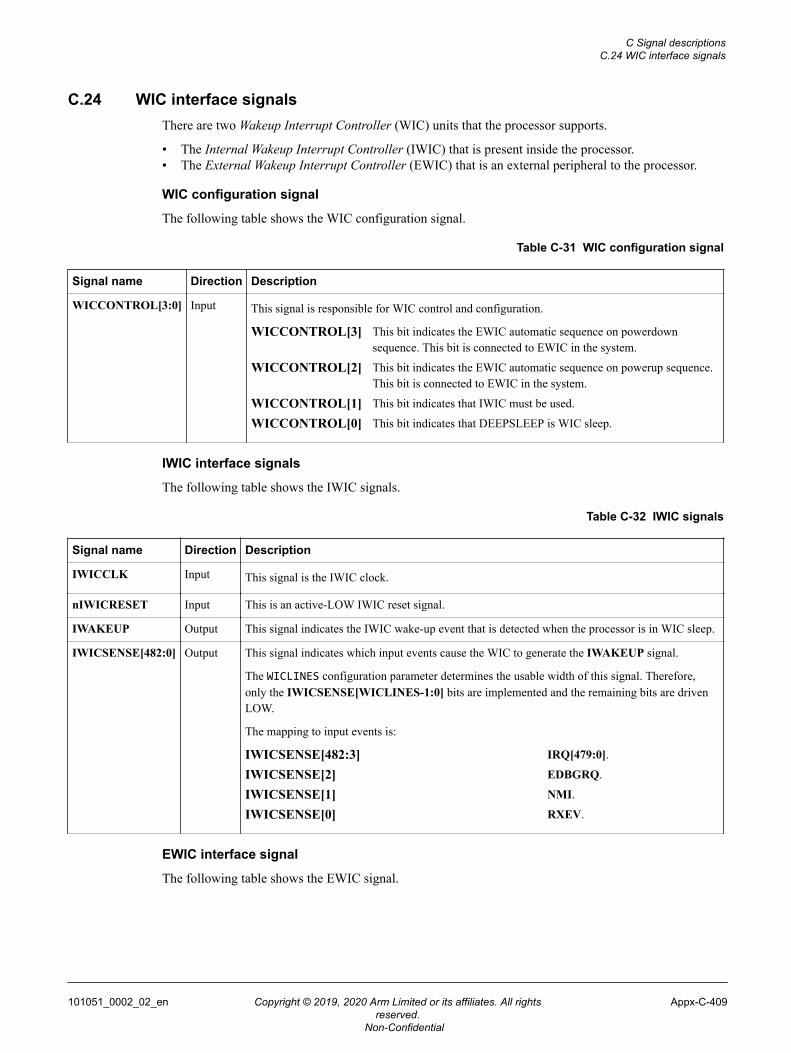
C.24 WIC interface signalsThere are two Wakeup Interrupt Controller (WIC) units that the processor supports.
• The Internal Wakeup Interrupt Controller (IWIC) that is present inside the processor.• The External Wakeup Interrupt Controller (EWIC) that is an external peripheral to the processor.
WIC configuration signal
The following table shows the WIC configuration signal.
Table C-31 WIC configuration signal
Signal name Direction Description
WICCONTROL[3:0] Input This signal is responsible for WIC control and configuration.
WICCONTROL[3] This bit indicates the EWIC automatic sequence on powerdownsequence. This bit is connected to EWIC in the system.
WICCONTROL[2] This bit indicates the EWIC automatic sequence on powerup sequence.This bit is connected to EWIC in the system.
WICCONTROL[1] This bit indicates that IWIC must be used.
WICCONTROL[0] This bit indicates that DEEPSLEEP is WIC sleep.
IWIC interface signals
The following table shows the IWIC signals.
Table C-32 IWIC signals
Signal name Direction Description
IWICCLK Input This signal is the IWIC clock.
nIWICRESET Input This is an active-LOW IWIC reset signal.
IWAKEUP Output This signal indicates the IWIC wake-up event that is detected when the processor is in WIC sleep.
IWICSENSE[482:0] Output This signal indicates which input events cause the WIC to generate the IWAKEUP signal.
The WICLINES configuration parameter determines the usable width of this signal. Therefore,only the IWICSENSE[WICLINES-1:0] bits are implemented and the remaining bits are drivenLOW.
The mapping to input events is:
IWICSENSE[482:3] IRQ[479:0].
IWICSENSE[2] EDBGRQ.
IWICSENSE[1] NMI.
IWICSENSE[0] RXEV.
EWIC interface signal
The following table shows the EWIC signal.
C Signal descriptionsC.24 WIC interface signals
101051_0002_02_en Copyright © 2019, 2020 Arm Limited or its affiliates. All rightsreserved.
Appx-C-409
Non-Confidential
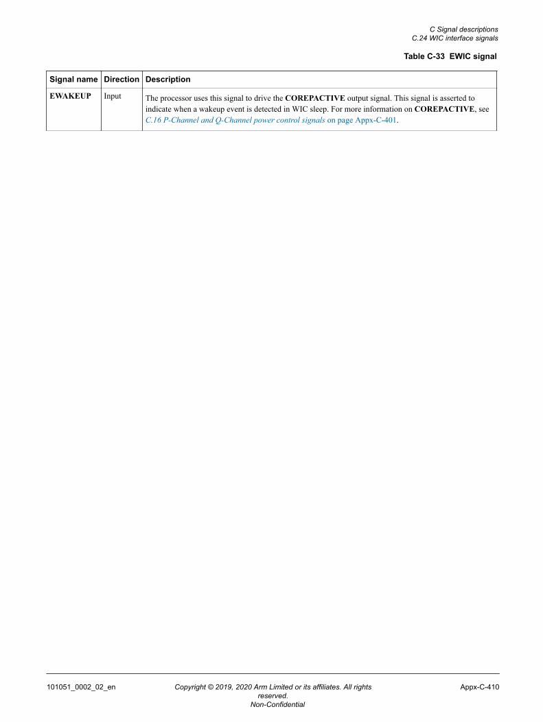
Table C-33 EWIC signal
Signal name Direction Description
EWAKEUP Input The processor uses this signal to drive the COREPACTIVE output signal. This signal is asserted toindicate when a wakeup event is detected in WIC sleep. For more information on COREPACTIVE, seeC.16 P-Channel and Q-Channel power control signals on page Appx-C-401.
C Signal descriptionsC.24 WIC interface signals
101051_0002_02_en Copyright © 2019, 2020 Arm Limited or its affiliates. All rightsreserved.
Appx-C-410
Non-Confidential
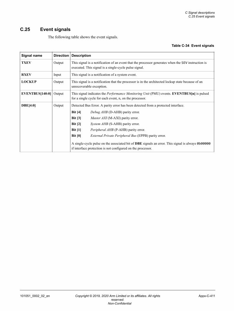
C.25 Event signalsThe following table shows the event signals.
Table C-34 Event signals
Signal name Direction Description
TXEV Output This signal is a notification of an event that the processor generates when the SEV instruction isexecuted. This signal is a single-cycle pulse signal.
RXEV Input This signal is a notification of a system event.
LOCKUP Output This signal is a notification that the processor is in the architected lockup state because of anunrecoverable exception.
EVENTBUS[140:0] Output This signal indicates the Performance Monitoring Unit (PMU) events. EVENTBUS[n] is pulsedfor a single cycle for each event, n, on the processor.
DBE[4:0] Output Detected Bus Error. A parity error has been detected from a protected interface.
Bit [4] Debug AHB (D-AHB) parity error.
Bit [3] Master AXI (M-AXI) parity error.
Bit [2] System AHB (S-AHB) parity error.
Bit [1] Peripheral AHB (P-AHB) parity error.
Bit [0] External Private Peripheral Bus (EPPB) parity error.
A single-cycle pulse on the associated bit of DBE signals an error. This signal is always 0b00000if interface protection is not configured on the processor.
C Signal descriptionsC.25 Event signals
101051_0002_02_en Copyright © 2019, 2020 Arm Limited or its affiliates. All rightsreserved.
Appx-C-411
Non-Confidential
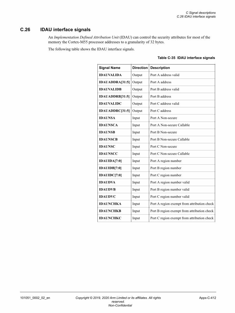
C.26 IDAU interface signalsAn Implementation Defined Attribution Unit (IDAU) can control the security attributes for most of thememory the Cortex-M55 processor addresses to a granularity of 32 bytes.
The following table shows the IDAU interface signals.
Table C-35 IDAU interface signals
Signal Name Direction Description
IDAUVALIDA Output Port A address valid
IDAUADDRA[31:5] Output Port A address
IDAUVALIDB Output Port B address valid
IDAUADDRB[31:5] Output Port B address
IDAUVALIDC Output Port C address valid
IDAUADDRC[31:5] Output Port C address
IDAUNSA Input Port A Non-secure
IDAUNSCA Input Port A Non-secure Callable
IDAUNSB Input Port B Non-secure
IDAUNSCB Input Port B Non-secure Callable
IDAUNSC Input Port C Non-secure
IDAUNSCC Input Port C Non-secure Callable
IDAUIDA[7:0] Input Port A region number
IDAUIDB[7:0] Input Port B region number
IDAUIDC[7:0] Input Port C region number
IDAUDVA Input Port A region number valid
IDAUDVB Input Port B region number valid
IDAUDVC Input Port C region number valid
IDAUNCHKA Input Port A region exempt from attribution check
IDAUNCHKB Input Port B region exempt from attribution check
IDAUNCHKC Input Port C region exempt from attribution check
C Signal descriptionsC.26 IDAU interface signals
101051_0002_02_en Copyright © 2019, 2020 Arm Limited or its affiliates. All rightsreserved.
Appx-C-412
Non-Confidential
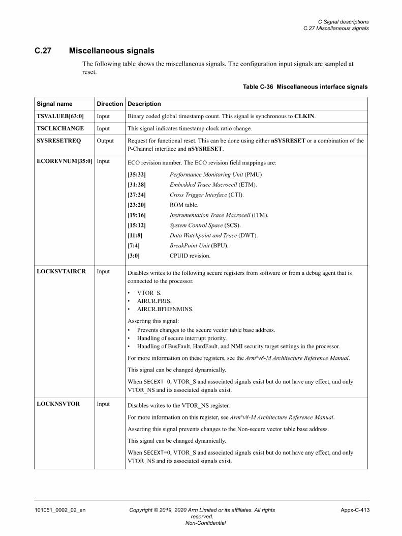
C.27 Miscellaneous signalsThe following table shows the miscellaneous signals. The configuration input signals are sampled atreset.
Table C-36 Miscellaneous interface signals
Signal name Direction Description
TSVALUEB[63:0] Input Binary coded global timestamp count. This signal is synchronous to CLKIN.
TSCLKCHANGE Input This signal indicates timestamp clock ratio change.
SYSRESETREQ Output Request for functional reset. This can be done using either nSYSRESET or a combination of theP-Channel interface and nSYSRESET.
ECOREVNUM[35:0] Input ECO revision number. The ECO revision field mappings are:
[35:32] Performance Monitoring Unit (PMU)
[31:28] Embedded Trace Macrocell (ETM).
[27:24] Cross Trigger Interface (CTI).
[23:20] ROM table.
[19:16] Instrumentation Trace Macrocell (ITM).
[15:12] System Control Space (SCS).
[11:8] Data Watchpoint and Trace (DWT).
[7:4] BreakPoint Unit (BPU).
[3:0] CPUID revision.
LOCKSVTAIRCR Input Disables writes to the following secure registers from software or from a debug agent that isconnected to the processor.
• VTOR_S.• AIRCR.PRIS.• AIRCR.BFHFNMINS.
Asserting this signal:• Prevents changes to the secure vector table base address.• Handling of secure interrupt priority.• Handling of BusFault, HardFault, and NMI security target settings in the processor.
For more information on these registers, see the Arm®v8-M Architecture Reference Manual.
This signal can be changed dynamically.
When SECEXT=0, VTOR_S and associated signals exist but do not have any effect, and onlyVTOR_NS and its associated signals exist.
LOCKNSVTOR Input Disables writes to the VTOR_NS register.
For more information on this register, see Arm®v8-M Architecture Reference Manual.
Asserting this signal prevents changes to the Non-secure vector table base address.
This signal can be changed dynamically.
When SECEXT=0, VTOR_S and associated signals exist but do not have any effect, and onlyVTOR_NS and its associated signals exist.
C Signal descriptionsC.27 Miscellaneous signals
101051_0002_02_en Copyright © 2019, 2020 Arm Limited or its affiliates. All rightsreserved.
Appx-C-413
Non-Confidential
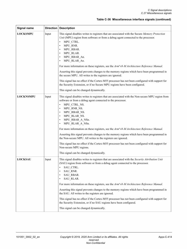
Table C-36 Miscellaneous interface signals (continued)
Signal name Direction Description
LOCKSMPU Input This signal disables writes to registers that are associated with the Secure Memory ProtectionUnit (MPU) region from software or from a debug agent connected to the processor.• MPU_CTRL.• MPU_RNR.• MPU_RBAR.• MPU_RLAR.• MPU_RBAR_An.• MPU_RLAR_An.
For more information on these registers, see the Arm®v8-M Architecture Reference Manual.
Asserting this signal prevents changes to the memory regions which have been programmed inthe secure MPU. All writes to the registers are ignored.
This signal has no effect if the Cortex-M55 processor has not been configured with support forthe Security Extension, or if no Secure MPU regions have been configured.
This signal can be changed dynamically.
LOCKNSMPU Input This signal disables writes to registers that are associated with the Non-secure MPU region fromsoftware or from a debug agent connected to the processor.• MPU_CTRL_NS.• MPU_RNR_NS.• MPU_RBAR_NS.• MPU_RLAR_NS.• MPU_RBAR_A_NSn.• MPU_RLAR_A_NSn.
For more information on these registers, see the Arm®v8-M Architecture Reference Manual.
Asserting this signal prevents changes to the memory regions which have been programmed inthe Non-secure MPU. All writes to the registers are ignored.
This signal has no effect if the Cortex-M55 processor has not been configured with support forNon-secure MPU regions.
This signal can be changed dynamically.
LOCKSAU Input This signal disables writes to registers that are associated with the Security Attribution Unit(SAU) region from software or from a debug agent connected to the processor.• SAU_CTRL.• SAU_RNR.• SAU_RBAR.• SAU_RLAR.
For more information on these registers, see the Arm®v8-M Architecture Reference Manual.
Asserting this signal prevents changes to the memory regions which have been programmed inthe SAU. All writes to the registers are ignored.
This signal has no effect if the Cortex-M55 processor has not been configured with support forthe Security Extension, or if no SAU regions have been configured.
This signal can be changed dynamically.
C Signal descriptionsC.27 Miscellaneous signals
101051_0002_02_en Copyright © 2019, 2020 Arm Limited or its affiliates. All rightsreserved.
Appx-C-414
Non-Confidential
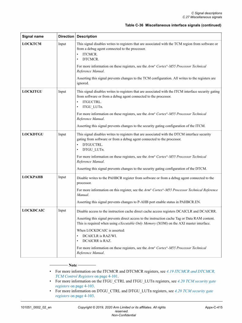
Table C-36 Miscellaneous interface signals (continued)
Signal name Direction Description
LOCKTCM Input This signal disables writes to registers that are associated with the TCM region from software orfrom a debug agent connected to the processor.• ITCMCR.• DTCMCR.
For more information on these registers, see the Arm® Cortex®-M55 Processor TechnicalReference Manual.
Asserting this signal prevents changes to the TCM configuration. All writes to the registers areignored.
LOCKITGU Input This signal disables writes to registers that are associated with the ITCM interface security gatingfrom software or from a debug agent connected to the processor.• ITGUCTRL.• ITGU_LUTn.
For more information on these registers, see the Arm® Cortex®-M55 Processor TechnicalReference Manual.
Asserting this signal prevents changes to the security gating configuration of the ITCM.
LOCKDTGU Input This signal disables writes to registers that are associated with the DTCM interface securitygating from software or from a debug agent connected to the processor.• DTGUCTRL.• DTGU_LUTn.
For more information on these registers, see the Arm® Cortex®-M55 Processor TechnicalReference Manual.
Asserting this signal prevents changes to the security gating configuration of the DTCM.
LOCKPAHB Input Disable writes to the PAHBCR register from software or from a debug agent connected to theprocessor.
For more information on this register, see the Arm® Cortex®-M55 Processor Technical ReferenceManual.
Asserting this signal prevents changes to P-AHB port enable status in PAHBCR.EN.
LOCKDCAIC Input Disable access to the instruction cache direct cache access registers DCAICLR and DCAICRR.
Asserting this signal prevents direct access to the instruction cache Tag or Data RAM content.This is required when using eXecutable Only Memory (XOM) on the AXI master interface.
When LOCKDCAIC is asserted:• DCAICLR is RAZ/WI.• DCAICRR is RAZ.
For more information on these registers, see the Arm® Cortex®-M55 Processor TechnicalReference Manual.
Note
• For more information on the ITCMCR and DTCMCR registers, see 4.19 ITCMCR and DTCMCR,TCM Control Registers on page 4-101.
• For more information on the ITGU_CTRL and ITGU_LUTn registers, see 4.20 TCM security gateregisters on page 4-103.
• For more information on DTGU_CTRL and DTGU_LUTn registers, see 4.20 TCM security gateregisters on page 4-103.
C Signal descriptionsC.27 Miscellaneous signals
101051_0002_02_en Copyright © 2019, 2020 Arm Limited or its affiliates. All rightsreserved.
Appx-C-415
Non-Confidential
• For more information on the PAHBCR register, see 4.14 PAHBCR, P-AHB Control Registeron page 4-90.
• For more information on the DCAICLR and DCAICRR registers, see 4.11.1 DCAICLR andDCADCLR, Direct Cache Access Location Registers on page 4-75 and 4.11.2 DCAICRR andDCADCRR, Direct Cache Access Read Registers on page 4-77.
C Signal descriptionsC.27 Miscellaneous signals
101051_0002_02_en Copyright © 2019, 2020 Arm Limited or its affiliates. All rightsreserved.
Appx-C-416
Non-Confidential
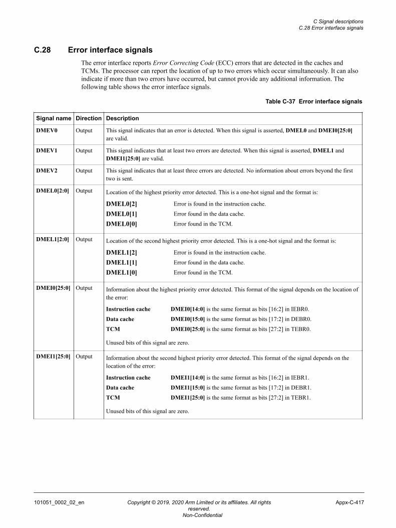
C.28 Error interface signalsThe error interface reports Error Correcting Code (ECC) errors that are detected in the caches andTCMs. The processor can report the location of up to two errors which occur simultaneously. It can alsoindicate if more than two errors have occurred, but cannot provide any additional information. Thefollowing table shows the error interface signals.
Table C-37 Error interface signals
Signal name Direction Description
DMEV0 Output This signal indicates that an error is detected. When this signal is asserted, DMEL0 and DMEI0[25:0]are valid.
DMEV1 Output This signal indicates that at least two errors are detected. When this signal is asserted, DMEL1 andDMEI1[25:0] are valid.
DMEV2 Output This signal indicates that at least three errors are detected. No information about errors beyond the firsttwo is sent.
DMEL0[2:0] Output Location of the highest priority error detected. This is a one-hot signal and the format is:
DMEL0[2] Error is found in the instruction cache.
DMEL0[1] Error found in the data cache.
DMEL0[0] Error found in the TCM.
DMEL1[2:0] Output Location of the second highest priority error detected. This is a one-hot signal and the format is:
DMEL1[2] Error is found in the instruction cache.
DMEL1[1] Error found in the data cache.
DMEL1[0] Error found in the TCM.
DMEI0[25:0] Output Information about the highest priority error detected. This format of the signal depends on the location ofthe error:
Instruction cache DMEI0[14:0] is the same format as bits [16:2] in IEBR0.
Data cache DMEI0[15:0] is the same format as bits [17:2] in DEBR0.
TCM DMEI0[25:0] is the same format as bits [27:2] in TEBR0.
Unused bits of this signal are zero.
DMEI1[25:0] Output Information about the second highest priority error detected. This format of the signal depends on thelocation of the error:
Instruction cache DMEI1[14:0] is the same format as bits [16:2] in IEBR1.
Data cache DMEI1[15:0] is the same format as bits [17:2] in DEBR1.
TCM DMEI1[25:0] is the same format as bits [27:2] in TEBR1.
Unused bits of this signal are zero.
C Signal descriptionsC.28 Error interface signals
101051_0002_02_en Copyright © 2019, 2020 Arm Limited or its affiliates. All rightsreserved.
Appx-C-417
Non-Confidential
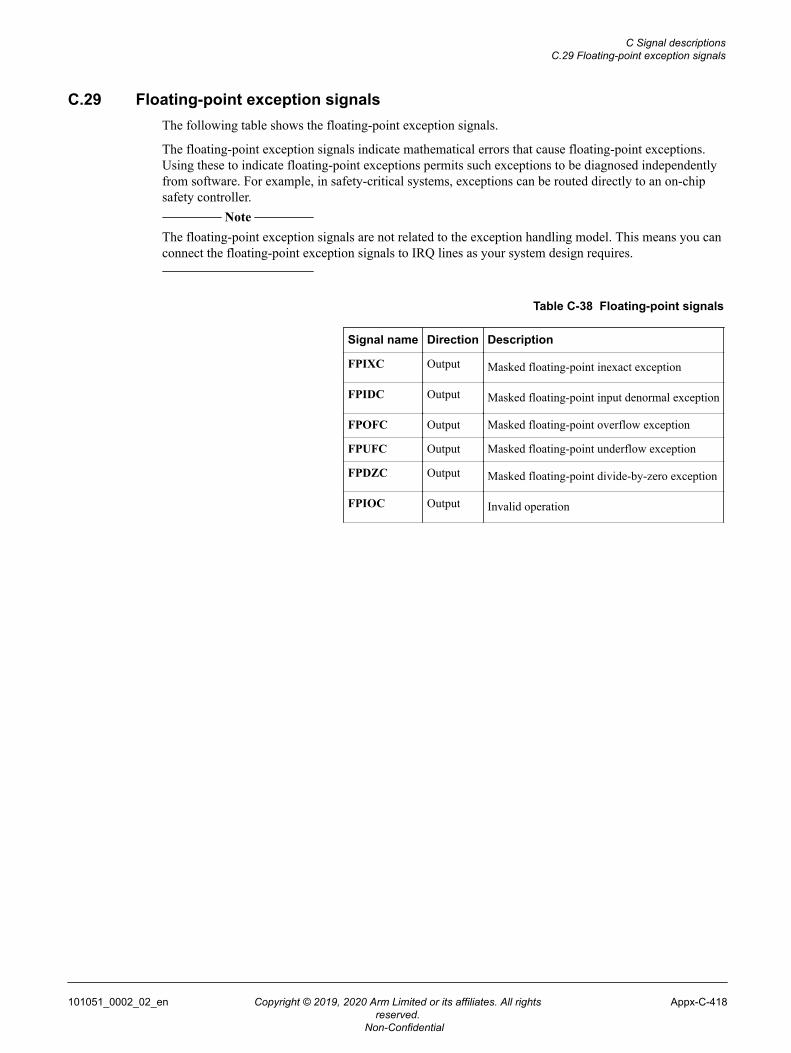
C.29 Floating-point exception signalsThe following table shows the floating-point exception signals.
The floating-point exception signals indicate mathematical errors that cause floating-point exceptions.Using these to indicate floating-point exceptions permits such exceptions to be diagnosed independentlyfrom software. For example, in safety-critical systems, exceptions can be routed directly to an on-chipsafety controller.
Note
The floating-point exception signals are not related to the exception handling model. This means you canconnect the floating-point exception signals to IRQ lines as your system design requires.
Table C-38 Floating-point signals
Signal name Direction Description
FPIXC Output Masked floating-point inexact exception
FPIDC Output Masked floating-point input denormal exception
FPOFC Output Masked floating-point overflow exception
FPUFC Output Masked floating-point underflow exception
FPDZC Output Masked floating-point divide-by-zero exception
FPIOC Output Invalid operation
C Signal descriptionsC.29 Floating-point exception signals
101051_0002_02_en Copyright © 2019, 2020 Arm Limited or its affiliates. All rightsreserved.
Appx-C-418
Non-Confidential
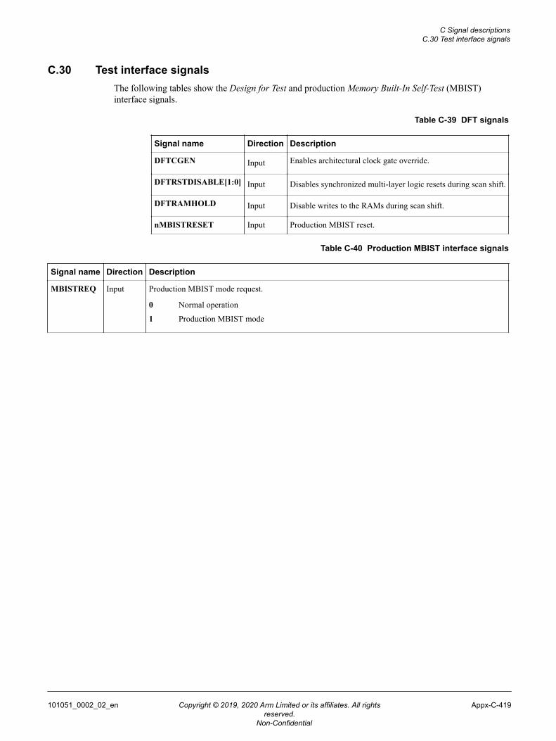
C.30 Test interface signalsThe following tables show the Design for Test and production Memory Built-In Self-Test (MBIST)interface signals.
Table C-39 DFT signals
Signal name Direction Description
DFTCGEN Input Enables architectural clock gate override.
DFTRSTDISABLE[1:0] Input Disables synchronized multi-layer logic resets during scan shift.
DFTRAMHOLD Input Disable writes to the RAMs during scan shift.
nMBISTRESET Input Production MBIST reset.
Table C-40 Production MBIST interface signals
Signal name Direction Description
MBISTREQ Input Production MBIST mode request.
0 Normal operation
1 Production MBIST mode
C Signal descriptionsC.30 Test interface signals
101051_0002_02_en Copyright © 2019, 2020 Arm Limited or its affiliates. All rightsreserved.
Appx-C-419
Non-Confidential
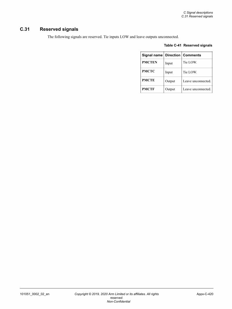
C.31 Reserved signalsThe following signals are reserved. Tie inputs LOW and leave outputs unconnected.
Table C-41 Reserved signals
Signal name Direction Comments
PMCTEN Input Tie LOW.
PMCTC Input Tie LOW.
PMCTE Output Leave unconnected.
PMCTF Output Leave unconnected.
C Signal descriptionsC.31 Reserved signals
101051_0002_02_en Copyright © 2019, 2020 Arm Limited or its affiliates. All rightsreserved.
Appx-C-420
Non-Confidential
Appendix DUNPREDICTABLE Behaviors
This appendix summarizes the behavior of the Cortex-M55 processor in cases where the Armv8.1‑Marchitecture is UNPREDICTABLE.
It contains the following sections:• D.1 Use of instructions defined in architecture variants on page Appx-D-422.• D.2 Use of Program Counter - R15 encoding on page Appx-D-423.• D.3 Use of Stack Pointer - as a general-purpose register R13 on page Appx-D-424.• D.4 Register list in load and store multiple instructions on page Appx-D-425.• D.5 Exception-continuable instructions on page Appx-D-426.• D.6 Stack limit checking on page Appx-D-427.• D.7 UNPREDICTABLE instructions within an IT block on page Appx-D-428.• D.8 Memory access and address space on page Appx-D-429.• D.9 MPU programming on page Appx-D-430.• D.10 Miscellaneous UNPREDICTABLE instruction behavior on page Appx-D-431.
101051_0002_02_en Copyright © 2019, 2020 Arm Limited or its affiliates. All rightsreserved.
Appx-D-421
Non-Confidential
D.1 Use of instructions defined in architecture variantsAn instruction that is provided by one or more of the architecture extensions is either UNPREDICTABLE orUNDEFINED in an implementation that does not include those extensions.
In the Cortex-M55 processor, all instructions that are not explicitly supported generate an UNDEFINSTRUsageFault exception.
D UNPREDICTABLE BehaviorsD.1 Use of instructions defined in architecture variants
101051_0002_02_en Copyright © 2019, 2020 Arm Limited or its affiliates. All rightsreserved.
Appx-D-422
Non-Confidential
D.2 Use of Program Counter - R15 encodingR15 is UNPREDICTABLE as a source or destination in most data processing operations. R15 is alsoUNPREDICTABLE as a transfer register in certain load/store instructions. Examples of such instructionsinclude LDRT, LDRH, and LDRB.
In the Cortex-M55 processor, the use of R15 as a named register specifier for any source or destinationregister that is indicated as UNPREDICTABLE generates an UNDEFINSTR UsageFault exception.
D UNPREDICTABLE BehaviorsD.2 Use of Program Counter - R15 encoding
101051_0002_02_en Copyright © 2019, 2020 Arm Limited or its affiliates. All rightsreserved.
Appx-D-423
Non-Confidential
D.3 Use of Stack Pointer - as a general-purpose register R13R13 is defined in the Thumb instruction set so that its use is primarily as a stack pointer. R13 is normallyidentified as stack pointer, SP in Thumb instructions.
In 32-bit Thumb instructions, if you use SP as a general-purpose register beyond the architecturallydefined constraints, the results are UNPREDICTABLE.
In the Cortex-M55 processor, the use of R13 as a named register specifier for any source or destinationregister that is indicated as UNPREDICTABLE generates an UNDEFINSTR UsageFault exception.
In the architecture where the use of R13 as a general-purpose register is defined, bits[1:0] of the registermust be treated as SBZP. Writing a nonzero value to bits [1:0] results in UNPREDICTABLE behavior. In theCortex-M55 processor, bits [1:0] of R13 are always RAZ/WI.
D UNPREDICTABLE BehaviorsD.3 Use of Stack Pointer - as a general-purpose register R13
101051_0002_02_en Copyright © 2019, 2020 Arm Limited or its affiliates. All rightsreserved.
Appx-D-424
Non-Confidential
D.4 Register list in load and store multiple instructionsLoad and Store Multiple instructions (LDM, STM, PUSH, POP VLDM, and VSTM) transfer multiple registers toand from consecutive memory locations using an address from a base register, which can be optionallywritten back when the operation is complete.
The registers are selected from a list encoded in the instruction. Some of these encodings areUNPREDICTABLE.
In the Cortex-M55 processor:• If the number of registers loaded is zero, then the instruction is a No Operation (NOP). If the number
of registers loaded is one, the single register is loaded.• If R13 is specified in the list, an UNDEFINED exception occurs.• For a Load Multiple, if PC is specified in the list and the instruction is in an IT block and is not the
final instruction, a fault is not generated. The branch is taken and the IT state is cleared.• For a Store Multiple instruction, if PC is specified in the list, an UNDEFINED exception occurs.• For a Load Multiple instruction, if base writeback is specified and the register to be written back is
also in the list to be loaded, the instruction performs all the loads in the specified addressing modeand the register being written back takes the loaded value.
• For a Store Multiple instruction, if base writeback is specified and the register to be written back isalso the first register in the list to be stored, the value stored is the initial base register value. The baseregister is written back with the expected updated value. If the register to be written back is not thefirst register in the list, then it takes the updated value.
• For a floating-point Load or Store Multiple instruction, VLDM, VSTM VPUSH, and VPOP, if the registerlist extends beyond S63 or D31, then the Cortex-M55 processor ignores all registers that are greaterthan S31 or D15. If it has a writeback, then the base register becomes UNKNOWN.
D UNPREDICTABLE BehaviorsD.4 Register list in load and store multiple instructions
101051_0002_02_en Copyright © 2019, 2020 Arm Limited or its affiliates. All rightsreserved.
Appx-D-425
Non-Confidential
D.5 Exception-continuable instructionsTo improve interrupt response and increase processing throughput, the processor can take an interruptduring the execution of a Load Multiple or Store Multiple instruction, and continue execution of theinstruction after returning from the interrupt. During the interrupt processing, the EPSR.ICI bit holds thecontinuation state of the Load Multiple or Store Multiple instruction.
In the Cortex-M55 processor, if an exception-continuable instruction is interrupted, then modification ofthe EPSR.ICI bits by either the software or a debugger might generate an INVSTATE UsageFaultexception when re-execution of the interrupted instruction is attempted.
This includes the architecturally UNPREDICTABLE cases of:• Not a register in the register list of the Load Multiple or Store Multiple instruction.• The first register in the register list of the Load Multiple or Store Multiple instruction.
The Cortex-M55 processor also generates an INVSTATE UsageFault exception if the ICI bits are set toany non-zero value for an integer Load Multiple instruction with the base register in the register list, andICI set to a greater register number than the base register. This is because these instructions are noteligible for continuation.
D UNPREDICTABLE BehaviorsD.5 Exception-continuable instructions
101051_0002_02_en Copyright © 2019, 2020 Arm Limited or its affiliates. All rightsreserved.
Appx-D-426
Non-Confidential
D.6 Stack limit checkingThe Armv8.1‑M architecture defines the instructions which are subject to stack limit checking whenoperating on SP.
It states that it is UNKNOWN whether a stack limit check is performed on any use of the SP that wasUNPREDICTABLE in Armv7‑M and Armv6‑M. In the Cortex-M55 processor, these UNPREDICTABLE cases arewhen R13 is used as a general-purpose register in instructions. In these circumstances, the processorgenerates an UNDEFINSTR UsageFault exception.
D UNPREDICTABLE BehaviorsD.6 Stack limit checking
101051_0002_02_en Copyright © 2019, 2020 Arm Limited or its affiliates. All rightsreserved.
Appx-D-427
Non-Confidential
D.7 UNPREDICTABLE instructions within an IT blockInstructions executed in an IT block which change the PC are architecturally UNPREDICTABLE unless theyare the last instruction in the block.
In the Cortex-M55 processor:• Conditional branch instructions (Bcond label) always generate an UNCONDITIONAL
UNDEFINSTR UsageFault exception.• Unconditional branch instructions (B label) which are not the last instructions in the IT block
execute normally.• Branch with link instructions (BL label) which are not the last instructions in the IT block execute
normally.• BLX PC is always UNPREDICTABLE and generates an UNDEFINSTR UsageFault exception.• Branch and exchange instructions (BX Rm) which are not the last instructions in the IT block execute
normally.• Compare and Branch instruction, CBNZ and CBZ always generate an UNCONDITIONAL
UNDEFINSTR UsageFault exception.• Table branch instructions (TBB and TBH) which are not the last instructions in the IT block execute
normally.• An IT instruction inside another IT block always generates an UNCONDITIONAL UNDEFINSTR
UsageFault exception.• If the Floating-point Extension is included and one of the following instructions is executed in an IT
block, the instruction generates an unconditional UNCONDITIONAL UNDEFINSTR UsageFaultexception:— VCVTA— VCVTN— VCVTP— VCVTM— VMAXNM— VMINNM— VRINTA— VRINTN— VRINTP— VRINTM— VSEL
• CPS instructions always generate an UNCONDITIONAL UNDEFINSTR UsageFault exception.
D UNPREDICTABLE BehaviorsD.7 UNPREDICTABLE instructions within an IT block
101051_0002_02_en Copyright © 2019, 2020 Arm Limited or its affiliates. All rightsreserved.
Appx-D-428
Non-Confidential
D.8 Memory access and address spaceIn the Armv8.1‑M architecture, there are memory accesses that result in UNPREDICTABLE behavior in theCortex-M55 processor.
The following table shows the memory accesses that are UNPREDICTABLE and the Cortex-M55 processorbehavior.
Table D-1 Memory accesses and Cortex-M55 processor behavior
Memory access Cortex-M55 processor behavior
Any access to memory from a load or store instruction or aninstruction fetch, which overflows the 32-bit address space.
These kinds of accesses wrap around to addresses at the start ofmemory.
For any access X, the bytes accessed by X must all have the samememory type attribute, otherwise the behavior of the access isUNPREDICTABLE. That is, an unaligned access that spans aboundary between different memory types is UNPREDICTABLE.
In the Cortex-M55 processor, each part of an access to a different32-byte aligned region is dealt with independently. If an MPU isincluded in the processor, each access to a different 32-byte regionmakes a new MPU lookup. If an MPU is not included, then thebehavior of the associated background region is taken intoaccount.
For any two memory accesses X and Y that are generated by thesame instruction, the bytes accessed by X and Y must all have thesame memory type attribute. Otherwise, the results areUNPREDICTABLE. For example, an LDC, LDM, LDRD, STC, STM,STRD, VSTM, VLDM, VPUSH, VPOP, VLDR, or VSTR that spans aboundary between Normal and Device memory isUNPREDICTABLE.
In the Cortex-M55 processor, each part of access to a different 32-byte aligned region is dealt with independently. If an MPU isincluded in the processor, each access to a different 32-bytealigned region makes a new MPU lookup. If an MPU is notincluded, then the behavior of the associated background region istaken into account.
Any instruction fetch must only access Normal memory. If itaccesses Device memory, the result is UNPREDICTABLE. Forexample, instruction fetches must not be performed to an area ofmemory that contains read-sensitive devices because there is noordering requirement between instruction fetches and explicitaccesses.
In the Cortex-M55 processor, fetches to Device memory are sentout to the system, indicated on the M-AXI interface as Device,unless the memory region is marked with the Execute Never (XN)memory attribute.
If the Security Extension is implemented, the behavior ofsequential instruction fetches that cross from Non-secure toSecure memory and fulfill the secure entry criteria specified in thearchitecture, including the presence of a Secure Gateway ( SG)instruction at the boundary of the secure memory area, isCONSTRAINED UNPREDICTABLE.
In the Cortex-M55 processor, this results in a fault (INVEP).
D UNPREDICTABLE BehaviorsD.8 Memory access and address space
101051_0002_02_en Copyright © 2019, 2020 Arm Limited or its affiliates. All rightsreserved.
Appx-D-429
Non-Confidential
D.9 MPU programmingThe Arm Protected Memory System Architecture (PMSA) includes many UNPREDICTABLE cases whenprogramming the MPU when it is included in an implementation.
In the Cortex-M55 processor:• Setting MPU_CTRL.ENABLE to 0 and MPU_CTRL.HFNMIEA to 1 is UNPREDICTABLE. This results
in all memory accesses using the default memory map including those from Exception Handlers witha priority less than one.
• If MPU_RNR is written with a region number greater than the number of regions defined in theMPU, then the value used is masked by one less than the number of regions defined. For example:— The number of regions defined is given as num_regions. The value written to MPU_RNR is given
as v.— num_regions=8 and v=9.— The effective region used is given as 9 & (8-1); region 1.
The number of regions available can be read from MPU_TYPE.DREGION.• Setting MPU_RBAR.SH to 1 is UNPREDICTABLE. This encoding is treated as Non-shareable.• The Attribute fields (MPU_ATTR) of the MPU_MAIR0 and MPU_MAIR1 registers include some
encodings which are UNPREDICTABLE.— If MPU_ATTR[7:4]!=0 and MPU_ATTR[3:0]==0 is UNPREDICTABLE, the attributes are treated as
Normal memory, Outer non-cacheable, Inner non-cacheable.— If MPU_ATTR[7:4]==0 and MPU_ATTR[1:0]!=0 is UNPREDICTABLE, the attributes are treated as
Device-nGnRE.• The external AMBA 5 AHB interface signals cannot distinguish between some of the memory
attribute encodings defined by the PMSA:— Normal transient memory is treated the same as Normal non-transient memory.— Device memory with Gathering or Reordering attributes (G, R) are always treated as non-
Gathering and non-Reordering. Early Write Acknowledgment attributes (E, nE) are supported onthe Cortex-M55 AHB5 interfaces.
D UNPREDICTABLE BehaviorsD.9 MPU programming
101051_0002_02_en Copyright © 2019, 2020 Arm Limited or its affiliates. All rightsreserved.
Appx-D-430
Non-Confidential
D.10 Miscellaneous UNPREDICTABLE instruction behaviorThis section documents the behavior of the Cortex-M55 processor in a number of miscellaneousUNPREDICTABLE instruction scenarios:
• Load instructions, which specify writeback of the base register, are UNPREDICTABLE if the base registerto be written back matches the register to be loaded (Rn==Rt). In the Cortex-M55 processor, the baseregister is updated to the loaded value.
• Store instructions which specify writeback of the base register are UNPREDICTABLE if the base registerto be written back matches the register to be stored (Rn==Rt). In the Cortex-M55 processor, the valuestored is the initial base register value. The base register is then written back with the expectedupdated value.
• Multiply and Multiply accumulate instructions which write a 64-bit result using two registers, SMULL,SMLAL, SMLALBB, SMLALBT, SMLALTB, SMLALTT, SMLALD, SMLALDX, SMLSLD, SMLSLDX, UMULL, andUMAAL are UNPREDICTABLE if the two registers are the same (RdHi==RdLo). In the Cortex-M55processor, these cases generate an UNDEFINSTR UsageFault exception.
• Floating-point instructions which transfer between two registers and either two single-precisionregisters or one double-precision register, VMOV Rt, Rt2, Dm and VMOV Rt, Rt2, Sm, Sm1 areUNPREDICTABLE if the two registers are the same (Rt==Rt2). In the Cortex-M55 processor, these casesgenerate an UNDEFINSTR UsageFault exception.
D UNPREDICTABLE BehaviorsD.10 Miscellaneous UNPREDICTABLE instruction behavior
101051_0002_02_en Copyright © 2019, 2020 Arm Limited or its affiliates. All rightsreserved.
Appx-D-431
Non-Confidential
Appendix ERevisions
This appendix describes the technical changes between released issues of this book.
It contains the following section:• E.1 Revisions on page Appx-E-433.
101051_0002_02_en Copyright © 2019, 2020 Arm Limited or its affiliates. All rightsreserved.
Appx-E-432
Non-Confidential
E.1 RevisionsThe following tables show any significant technical changes between released issues of this book.
Table E-1 Issue 0000-02
Change Location
First Beta release for r0p0 -
Table E-2 Differences between issue 0000-02 and 0000-04
Change Location
First limited access release for r0p0 -
Document structure has changed. Entire document
Extension Processing Unit chapter renamed to Floating-point and MVE support
Chapter 13 Floating-point and MVE support on page 13-246
Memory Authentication Unit chapter renamed toMemory Authentication
Memory Authentication Unit on page 2-30
Performance Monitoring Unit chapter renamed toPerformance Monitoring Unit Extension
Chapter 15 Performance Monitoring Unit Extension on page 15-265
MAU block diagram added 2.1.3 Memory components on page 2-30
Security section added 2.3 Security on page 2-36
Functional safety and reliability section added 2.4 Reliability on page 2-37
Power intent section added 2.5 Power intent on page 2-38
System Control chapter renamed to System registers Chapter 4 System registers on page 4-50
Implementation control register summary added 4.7 Implementation control register summary on page 4-67
• ACTLR bit 0 has changed.• ACTLR bit 2 has changed.• ACTLR bit 11 has changed.• ACTLR bit 18 has changed.
4.8 ACTLR, Auxiliary Control Register on page 4-68
More information added in CPDLPSTATE register bits4.16.1 CPDLPSTATE, Core Power Domain Low Power State Registeron page 4-92
Placement of RAS register descriptions changed indocument
10.5 RAS Extension registers on page 10-222
Placement of EWIC interrupt status access registerschanged in document
4.21 EWIC interrupt status access registers on page 4-108
Initialization chapter added Chapter 5 Initialization on page 5-111
Power mode definition table updated 6.4 Core P-Channel and power mode selection on page 6-130
• Distinction drawn between power mode andoperating mode in power management chapter
• Chapter sections restructured and more informationadded
Chapter 6 Power management on page 6-122
PPB memory region accesses table updated 7.3 Private Peripheral Bus on page 7-148
E RevisionsE.1 Revisions
101051_0002_02_en Copyright © 2019, 2020 Arm Limited or its affiliates. All rightsreserved.
Appx-E-433
Non-Confidential
Table E-2 Differences between issue 0000-02 and 0000-04 (continued)
Change Location
Unaligned accesses information updated to distinguishclearly between non-MVE and MVE loads and stores
7.4 Unaligned accesses on page 7-150
SFSR and SFAR registers added to SAU registersummary table
8.2.1 SAU register summary on page 8-157
Memory regions not controlled by SAU and IDAUsection updated
8.5 Memory regions not controlled by SAU and IDAU on page 8-162
Security attribution signals section updated 8.6 Security attribution signals on page 8-163
Memory system behavior section updated 9.3 Memory system behavior on page 9-175
Restrictions on AXI transfers section updated Restrictions on AXI transfers on page 9-184
Note describing types of burst transactions added• Area optimized configuration M-AXI attributes and transactions
on page 9-181• 9.6.2 S-AHB transfers on page 9-189
S-AHB availability and low power states section added 9.6.4 S-AHB availability and low power states on page 9-190
TCM interface protocol and Using TCM wait statessection removed from TRM and retained only in theIIM. The IIM is a confidential document available onlyto licensees
Arm® Cortex®-M55 Processor Integration and Implementation Manual
Accessing the caches section added 9.9.6 Accessing the caches on page 9-200
System cache support section updated 9.9.7 System cache support on page 9-201
DCAICRR data format for instruction cache tag RAMreads table updated
4.11 Direct cache access registers on page 4-75
Error processing in the L1 data and instruction cachesection updated
Error processing in the L1 data and instruction cache on page 10-214
PMU events table updated 15.2 PMU events on page 15-267
M-AXI read access poisoning section removed fromTRM and retained only in the IIM. The IIM is aconfidential document available only to licensees
Arm® Cortex®-M55 Processor Integration and Implementation Manual
Cortex-M55 processor ROM table components tableupdated
14.1.3 Processor ROM table identification and entries on page 14-255
DWT debug access control section updated 17.2 DWT debug access control on page 17-286
E RevisionsE.1 Revisions
101051_0002_02_en Copyright © 2019, 2020 Arm Limited or its affiliates. All rightsreserved.
Appx-E-434
Non-Confidential
Table E-2 Differences between issue 0000-02 and 0000-04 (continued)
Change Location
TPIU register descriptions added • B.2.14 CLAIMSET, Claim Tag Set Register on page Appx-B-363• B.2.15 CLAIMCLR, Claim Tag Clear Register on page Appx-B-364• B.2.16 TPIU_DEVID, Device Configuration Register
on page Appx-B-365• B.2.17 TPIU_DEVTYPE, Device Type Identifier Register
on page Appx-B-366• B.2.18 TPIU_PIDR4, Peripheral Identification Register 4
on page Appx-B-366• B.2.19 TPIU_PIDR5, Peripheral Identification Register 5
on page Appx-B-367• B.2.20 TPIU_PIDR6, Peripheral Identification Register 6
on page Appx-B-368• B.2.21 TPIU_PIDR7, Peripheral Identification Register 7
on page Appx-B-368• B.2.22 TPIU_PIDR0, Peripheral Identification Register 0
on page Appx-B-369• B.2.23 TPIU_PIDR1, Peripheral Identification Register 1
on page Appx-B-370• B.2.24 TPIU_PIDR2, Peripheral Identification Register 2
on page Appx-B-370• B.2.25 TPIU_PIDR3, Peripheral Identification Register 3
on page Appx-B-371• B.2.26 TPIU_ CIDR0, Component Identification Register 0
on page Appx-B-372• B.2.27 TPIU_ CIDR1, Component Identification Register 1
on page Appx-B-372• B.2.28 TPIU_ CIDR2, Component Identification Register 2
on page Appx-B-373• B.2.29 TPIU_ CIDR3, Component Identification Register 3
on page Appx-B-373
UNPREDICTABLE instructions within an IT block sectionupdated
D.7 UNPREDICTABLE instructions within an IT blockon page Appx-D-428
Memory access and address space section updated D.8 Memory access and address space on page Appx-D-429
Power management chapter structure changed. Somechanges include:• Permitted power mode and transitions displayed
before their descriptions.• Core P-Channel and power mode selection section
moved.• PDCORE, PDEPU, and PDRAMS low-power and
powerdown requirements information
Chapter 6 Power management on page 6-122
External coprocessors chapter structure changed Chapter 12 External coprocessors on page 12-237
Table E-3 Differences between issue 0000-04 and 0001-05
Change Location
First early access release for r0p1 -
Block diagram updated to include power domains 2.1 Cortex®-M55 processor components on page 2-27
E RevisionsE.1 Revisions
101051_0002_02_en Copyright © 2019, 2020 Arm Limited or its affiliates. All rightsreserved.
Appx-E-435
Non-Confidential
Table E-3 Differences between issue 0000-04 and 0001-05 (continued)
Change Location
Exclusive monitor section content updated to includeinformation about exclusive read accesses
3.3 Exclusive monitor on page 3-45
CPUID register reset value updated• 4.1 System control register summary on page 4-51• 4.2 Identification register summary on page 4-55• 4.4 CPUID, CPUID Base Register on page 4-61
DCADCRR.STATUS bit encoding information added4.11.2 DCAICRR and DCADCRR, Direct Cache Access Read Registerson page 4-77
MSCR bit 17 defined 4.13 MSCR, Memory System Control Register on page 4-87
Initializing the EPU section updated 5.3 Initializing the EPU on page 5-114
Programming the SAU section updated 5.4 Programming the SAU on page 5-115
Initializing the instruction and data cache section updated 5.5 Initializing the instruction and data cache on page 5-116
Enabling and preloading the TCM section updated 5.7 Enabling and preloading the TCM on page 5-119
Enabling the P-AHB interface section updated 5.9 Enabling the P-AHB interface on page 5-121
Operating mode transitions which change PDRAMS powerstate section updated
6.3.1 Operating mode transitions which change PDRAMS power stateon page 6-128
PDCORE low-power requirements section updated 6.6 PDCORE low-power requirements on page 6-135
PDEPU low-power requirements section updated 6.7 PDEPU low-power requirements on page 6-136
Unaligned accesses section updated 7.4 Unaligned accesses on page 7-150
Security check and fault response section updated toinclude information about debug accesses
8.8.4 Security check and fault response on page 8-169
Preventing Speculative accesses information updated inConsiderations for system design section
Considerations for system design on page 9-177
Table E-4 Differences between issue 0001-05 and 0002-01
Change Location
First release for r0p2 -
Stylistic changes made to block diagram. Technical detailsremain the same
2.1 Cortex®-M55 processor components on page 2-27
More information added about Security to provide morecontext
2.3 Security on page 2-36
AFSR register type corrected from RW to RO 4.1 System control register summary on page 4-51
CPUID reset value updated fro r0p2 version• 4.1 System control register summary on page 4-51• 4.2 Identification register summary on page 4-55• 4.4 CPUID, CPUID Base Register on page 4-61
Note added to reset value column for CPDLPSTATE register 4.16 Power mode control registers on page 4-92
CFGINFOSEL value 0x41 added as a reserved field 4.17.1 CFGINFOSEL, Processor configuration information selectionregister on page 4-95
NUMBLKS field description corrected4.20.2 ITGU_CFG and DTGU_CFG, ITGU and DTGU ConfigurationRegisters on page 4-104
E RevisionsE.1 Revisions
101051_0002_02_en Copyright © 2019, 2020 Arm Limited or its affiliates. All rightsreserved.
Appx-E-436
Non-Confidential
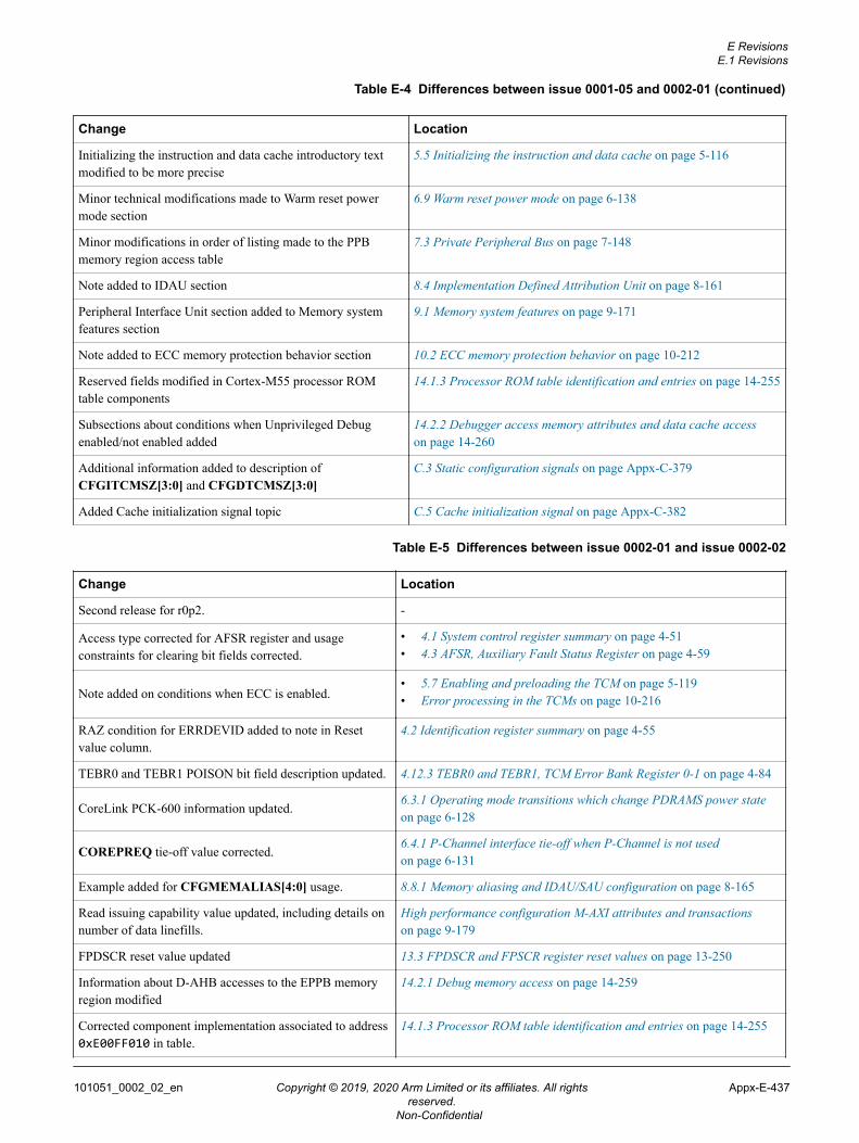
Table E-4 Differences between issue 0001-05 and 0002-01 (continued)
Change Location
Initializing the instruction and data cache introductory textmodified to be more precise
5.5 Initializing the instruction and data cache on page 5-116
Minor technical modifications made to Warm reset powermode section
6.9 Warm reset power mode on page 6-138
Minor modifications in order of listing made to the PPBmemory region access table
7.3 Private Peripheral Bus on page 7-148
Note added to IDAU section 8.4 Implementation Defined Attribution Unit on page 8-161
Peripheral Interface Unit section added to Memory systemfeatures section
9.1 Memory system features on page 9-171
Note added to ECC memory protection behavior section 10.2 ECC memory protection behavior on page 10-212
Reserved fields modified in Cortex-M55 processor ROMtable components
14.1.3 Processor ROM table identification and entries on page 14-255
Subsections about conditions when Unprivileged Debugenabled/not enabled added
14.2.2 Debugger access memory attributes and data cache accesson page 14-260
Additional information added to description ofCFGITCMSZ[3:0] and CFGDTCMSZ[3:0]
C.3 Static configuration signals on page Appx-C-379
Added Cache initialization signal topic C.5 Cache initialization signal on page Appx-C-382
Table E-5 Differences between issue 0002-01 and issue 0002-02
Change Location
Second release for r0p2. -
Access type corrected for AFSR register and usageconstraints for clearing bit fields corrected.
• 4.1 System control register summary on page 4-51• 4.3 AFSR, Auxiliary Fault Status Register on page 4-59
Note added on conditions when ECC is enabled.• 5.7 Enabling and preloading the TCM on page 5-119• Error processing in the TCMs on page 10-216
RAZ condition for ERRDEVID added to note in Resetvalue column.
4.2 Identification register summary on page 4-55
TEBR0 and TEBR1 POISON bit field description updated. 4.12.3 TEBR0 and TEBR1, TCM Error Bank Register 0-1 on page 4-84
CoreLink PCK-600 information updated.6.3.1 Operating mode transitions which change PDRAMS power stateon page 6-128
COREPREQ tie-off value corrected.6.4.1 P-Channel interface tie-off when P-Channel is not usedon page 6-131
Example added for CFGMEMALIAS[4:0] usage. 8.8.1 Memory aliasing and IDAU/SAU configuration on page 8-165
Read issuing capability value updated, including details onnumber of data linefills.
High performance configuration M-AXI attributes and transactionson page 9-179
FPDSCR reset value updated 13.3 FPDSCR and FPSCR register reset values on page 13-250
Information about D-AHB accesses to the EPPB memoryregion modified
14.2.1 Debug memory access on page 14-259
Corrected component implementation associated to address0xE00FF010 in table.
14.1.3 Processor ROM table identification and entries on page 14-255
E RevisionsE.1 Revisions
101051_0002_02_en Copyright © 2019, 2020 Arm Limited or its affiliates. All rightsreserved.
Appx-E-437
Non-Confidential
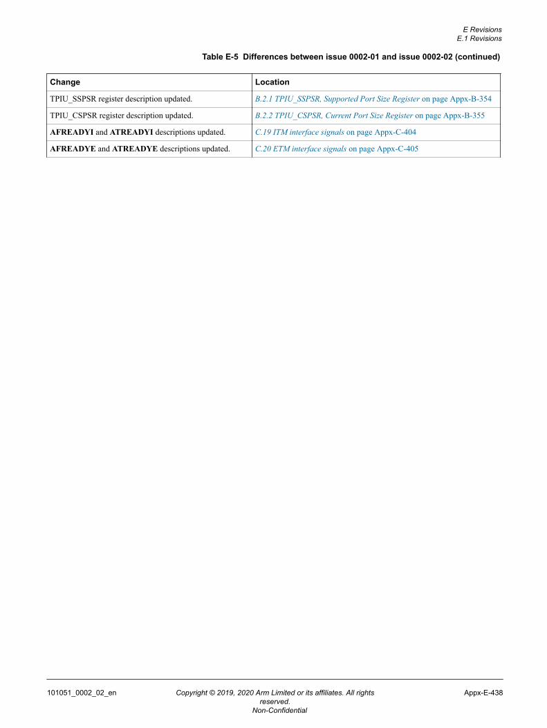
Table E-5 Differences between issue 0002-01 and issue 0002-02 (continued)
Change Location
TPIU_SSPSR register description updated. B.2.1 TPIU_SSPSR, Supported Port Size Register on page Appx-B-354
TPIU_CSPSR register description updated. B.2.2 TPIU_CSPSR, Current Port Size Register on page Appx-B-355
AFREADYI and ATREADYI descriptions updated. C.19 ITM interface signals on page Appx-C-404
AFREADYE and ATREADYE descriptions updated. C.20 ETM interface signals on page Appx-C-405
E RevisionsE.1 Revisions
101051_0002_02_en Copyright © 2019, 2020 Arm Limited or its affiliates. All rightsreserved.
Appx-E-438
Non-Confidential