Embed Size (px)
Citation preview

www.ti.com
FEATURES
APPLICATIONS
DESCRIPTION
4 mA
VREF VCC
SN65LVDS18, SN65LVP18
Q
A
VBB
GC
Y
Z
EN
4 mA
VREF VCC
SN65LVDS19, SN65LVP19
Q
A
VBB
Y
Z
EN
B
SN65LVDS18, SN65LVP18SN65LVDS19, SN65LVP19
SLLS624B–SEPTEMBER 2004–REVISED NOVEMBER 2005
2.5-V/3.3-V OSCILLATOR GAIN STAGE/BUFFERS
• 2-mm x 2-mm Small-OutlineNo-Lead Package• Low-Voltage PECL Input and Low-Voltage
PECL or LVDS Outputs• Clock Rates to 1 GHz
• PECL-to-LVDS Translation– 250-ps Output Transition Times• Clock Signal Amplification
– 0.12 ps Typical Intrinsic Phase Jitter– Less than 630 ps Propagation Delay Times
• 2.5-V or 3.3-V Supply Operation
These four devices are high frequency oscillator gain stages supporting both LVPECL or LVDS on the high gainoutputs in 3.3-V or 2.5-V systems. Additionally, provides the option of both single-ended input (PECL levels onthe SN65LVx18) and fully differential inputs on the SN65LVx19.
The SN65LVx18 provides the user a Gain Control (GC) for controlling the Q output from 300 mV to 860 mVeither by leaving it open (NC), grounded, or tied to VCC. (When left open, the Q output defaults to 575 mV.) TheQ on the SN65LVx19 defaults to 575 mV as well.
Both devices provide a voltage reference (VBB) of typically 1.35 V below VCC for use in receiving single-endedPECL input signals. When not used, VBB should be unconnected or open.
All devices are characterized for operation from –40°C to 85°C.
Please be aware that an important notice concerning availability, standard warranty, and use in critical applications of TexasInstruments semiconductor products and disclaimers thereto appears at the end of this data sheet.
PRODUCTION DATA information is current as of publication date. Copyright © 2004–2005, Texas Instruments IncorporatedProducts conform to specifications per the terms of the TexasInstruments standard warranty. Production processing does notnecessarily include testing of all parameters.
www.ti.com
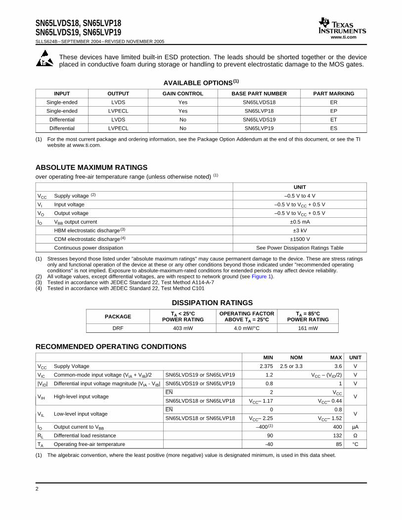
ABSOLUTE MAXIMUM RATINGS
DISSIPATION RATINGS
RECOMMENDED OPERATING CONDITIONS
SN65LVDS18, SN65LVP18SN65LVDS19, SN65LVP19SLLS624B–SEPTEMBER 2004–REVISED NOVEMBER 2005
These devices have limited built-in ESD protection. The leads should be shorted together or the deviceplaced in conductive foam during storage or handling to prevent electrostatic damage to the MOS gates.
AVAILABLE OPTIONS (1)
INPUT OUTPUT GAIN CONTROL BASE PART NUMBER PART MARKING
Single-ended LVDS Yes SN65LVDS18 ER
Single-ended LVPECL Yes SN65LVP18 EP
Differential LVDS No SN65LVDS19 ET
Differential LVPECL No SN65LVP19 ES
(1) For the most current package and ordering information, see the Package Option Addendum at the end of this document, or see the TIwebsite at www.ti.com.
over operating free-air temperature range (unless otherwise noted) (1)
UNIT
VCC Supply voltage (2) –0.5 V to 4 V
VI Input voltage –0.5 V to VCC + 0.5 V
VO Output voltage –0.5 V to VCC + 0.5 V
IO VBB output current ±0.5 mA
HBM electrostatic discharge (3) ±3 kV
CDM electrostatic discharge (4) ±1500 V
Continuous power dissipation See Power Dissipation Ratings Table
(1) Stresses beyond those listed under "absolute maximum ratings" may cause permanent damage to the device. These are stress ratingsonly and functional operation of the device at these or any other conditions beyond those indicated under "recommended operatingconditions" is not implied. Exposure to absolute-maximum-rated conditions for extended periods may affect device reliability.
(2) All voltage values, except differential voltages, are with respect to network ground (see Figure 1).(3) Tested in accordance with JEDEC Standard 22, Test Method A114-A-7(4) Tested in accordance with JEDEC Standard 22, Test Method C101
TA < 25°C OPERATING FACTOR TA = 85°CPACKAGE POWER RATING ABOVE TA = 25°C POWER RATING
DRF 403 mW 4.0 mW/°C 161 mW
MIN NOM MAX UNIT
VCC Supply Voltage 2.375 2.5 or 3.3 3.6 V
VIC Common-mode input voltage (VIA + VIB)/2 SN65LVDS19 or SN65LVP19 1.2 VCC – (VID/2) V
|VID| Differential input voltage magnitude |VIA - VIB| SN65LVDS19 or SN65LVP19 0.8 1 V
EN 2 VCCVIH High-level input voltage V
SN65LVDS18 or SN65LVP18 VCC– 1.17 VCC– 0.44
EN 0 0.8VIL Low-level input voltage V
SN65LVDS18 or SN65LVP18 VCC– 2.25 VCC– 1.52
IO Output current to VBB –400 (1) 400 µA
RL Differential load resistance 90 132 Ω
TA Operating free-air temperature -40 85 °C
(1) The algebraic convention, where the least positive (more negative) value is designated minimum, is used in this data sheet.
2

www.ti.com
ELECTRICAL CHARACTERISTICS
SN65LVDS18, SN65LVP18SN65LVDS19, SN65LVP19
SLLS624B–SEPTEMBER 2004–REVISED NOVEMBER 2005
over recommended operating conditions (unless otherwise noted)
PARAMETER TEST CONDITIONS MIN TYP (1) MAX UNIT
RL = 100 Ω, EN at 0 V, 30 36Other inputs openICC Supply current mA
Outputs unloaded, 17 22EN at 0 V, Other inputs open
VBB Reference voltage (2) IBB = –400 µA VCC– 1.44 VCC– 1.35 VCC– 1.25 V
IIH High-level input current, EN VI = 2 V –20 20
IIAH or IIBH High-level input current, A or B VI = VCC –20 20µA
IIL Low-level input current, EN VI = 0.8 V –20 20
IIAL or IIBL Low-level input current, A or B VI = GND –20 20
SN65LVDS18/19 Y AND Z OUTPUT CHARACTERISTICS
Differential output voltage|VOD| 247 340 454magnitude, |VOY– VOZ|mV
Change in differential output voltage∆|VOD| See Figure 1 and Figure 2 50magnitude between logic states
Steady-state common- mode outputVOC(SS) 1.125 1.375 Vvoltage (see Figure 3)
Change in steady-state∆VOC(SS) common-mode output voltage –50 50
between logic states See Figure 3 mVPeak-to-peak common-mode outputVOC(PP) 50 100voltage
IOYZ or IOZZ High-impedance output current EN at VCC, VO = 0 V or VCC –1 1 µA
IOYS or IOZS Short-circuit output current EN at 0 V, VOY or VOZ = 0 V –50 50mADifferential short-circuit output EN at 0 V,IOS(D) –12 12current, |IOY– IOZ| VOY = VOZ
SN65LVP18/19 Y AND Z OUTPUT CHARACTERISTICS
VOYH or High-level output voltage VCC– 1.13 VCC– 0.85VOZH 3.3 V; 50 Ω from Y and Zto VCC - 2 VVOYL or Low-level output voltage VCC– 1.87 VCC– 1.61VOZL
VVOYL or 2.5 V; 50 Ω from Y and ZLow-level output voltage VCC– 1.92 VCC– 1.61VOZL to VCC– 2 V
Differential output voltage|VOD| 0.6 0.8 1magnitude, |VOH– VOL|
IOYZ or IOZZ High-impedance output current EN at VCC, VO = 0 V or VCC –1 1 µA
Q OUTPUT CHARACTERISTICS (see Figure 1)
VOH High-level output voltage No load VCC– 0.94 V
GC Tied to GND, No load VCC– 1.22
VOL Low-level output voltage GC Open, No load VCC– 1.52 V
GC Tied to VCC, No load VCC– 1.82
GC Tied to GND 300
VO(pp) Peak-to-peak output voltage GC Open 575 mV
CGT Tied to VCC 860
(1) Typical values are at room temperature and with a VCC of 3.3 V.(2) Single-ended input operation is limited to VCC≥ 3.0 V.
3

www.ti.com
SWITCHING CHARACTERISTICS
PARAMETER MEASUREMENT INFORMATION
_+
A
GC
EN
Q
VBB
Z
Y
D.U.T.
GND
VCC
2
4
5
1
3
6
7
8
9
ICC
VCC
II
IIGC
IIA
IOY
IOZ
IBB 50
50
S1
_+VCC − 2 V
CL
+
−VOC
+
−VO
+
−VBB
+
−VOZ
+
−VOY
VI
_+
VIB
_+
VIA
SN65LVDS18, SN65LVP18SN65LVDS19, SN65LVP19SLLS624B–SEPTEMBER 2004–REVISED NOVEMBER 2005
over recommended operating conditions (unless otherwise noted)
PARAMETER TEST CONDITIONS MIN TYP (1) MAX UNIT
A to Q 340 460tPD Propagation delay time, tPLH or tPHL See Figure 4 ps
D to Y or Z 460 630
tSK(P) Pulse skew, |tPLH - tPHL| 20
VCC = 3.3 V 80tSK(PP) Part-to-part skew (2) ps
VCC = 2.5 V 130
LVDS, See Figure 4 140 250tr 20%-to-80% differential signal rise time ps
LVPECL, See Figure 4 190 300
LVDS, See Figure 4 140 250tf 20%-to-80% differential signal fall time ps
LVPECL, See Figure 4 210 300
tjit(per) RMS period jitter (3) 2 42-GHz 50%-duty-cycle square-wave input, psSee Figure 5tjit(cc) Peak cycle-to-cycle jitter (4) 17 24
tjit(ph) Intrinsic phase jitter 1 GHz 0.12 ps
Propagation delay time,tPHZ 30high-level-to-high-impedance output
Propagation delay time,tPLZ 30low-level-to-high-impedance outputSee Figure 6 ns
Propagation delay time,tPZH 30high-impedance-to-high-level output
Propagation delay time,tPZL 30high-impedance-to-low-level output
(1) Typical values are at room temperature and with a VCC of 3.3 V.(2) Part-to-part skew is the magnitude of the difference in propagation delay times between any specified terminals of two devices when
both devices operate with the same supply voltages, at the same temperature, and have identical packages and test circuits.(3) Period jitter is the deviation in cycle time of a signal with respect to the ideal period over a random sample of 100,000 cycles.(4) Cycle-to-cycle jitter is the variation in cycle time of a signal between adjacent cycles, over a random sample of 1,000 adjacent cycle
pairs.
(1) CL is the instrumentation and test fixture capacitance.
(2) S1 is open for the SN65LVDS18 and closed for the SN65LVP18.
Figure 1. Output Voltage Test Circuit and Voltage and Current Definitions for LVDS/LVP18
4

www.ti.com
_+
A
B
EN
Q
VBB
Z
Y
D.U.T.
GND
VCC
2
3
5
1
4
6
7
8
9
ICC
VCC
II
IIB
IIA
IOY
IOZ
IBB 50
50
S1
_+VCC − 2 V
CL
+
−VOC
+
−VO
+
−VBB
+
−VOZ
+
−VOY
VI
_+
VIB
_+
VIA
dVOC(SS)
INPUT
VOC
VOC(PP)
VIA
VIB
VOY − VOZ
tPHL t PLH
tf tr
1.125 V1.5 V
1.2 V
VCC
50%80% 100%
20%
SN65LVDS18, SN65LVP18SN65LVDS19, SN65LVP19
SLLS624B–SEPTEMBER 2004–REVISED NOVEMBER 2005
PARAMETER MEASUREMENT INFORMATION (continued)
(1) CL is the instrumentation and test fixture capacitance.
(2) S1 is open for the SN65LVDS19 and closed for the SN65LVP19.
Figure 2. Output Voltage Test Circuit and Voltage and Current Definitions for LVDS/LVP19
Figure 3. VOC Definitions
Figure 4. Propagation Delay and Transition Time Test Waveforms
5

www.ti.com
HP3104 Pattern Device Under Test TDS Oscilloscope withTJIT3 Analysis Pack
DC
Generator
50
50 Cable, X Y cm, SMA CoaxConnectors, 4 Places
50
VIA
VIB
VOY − VOZ
1.5 V
1.2 V
VCC
VI to EN
50%80%
100%
20%
1.4 V2 V
0.8 V
0 VPZH
t PHZ
t PZLt PLZ
t
SN65LVDS18, SN65LVP18SN65LVDS19, SN65LVP19SLLS624B–SEPTEMBER 2004–REVISED NOVEMBER 2005
PARAMETER MEASUREMENT INFORMATION (continued)
Figure 5. Jitter Measurement Setup
Figure 6. Enable and Disable Time Test Waveforms
6
www.ti.com
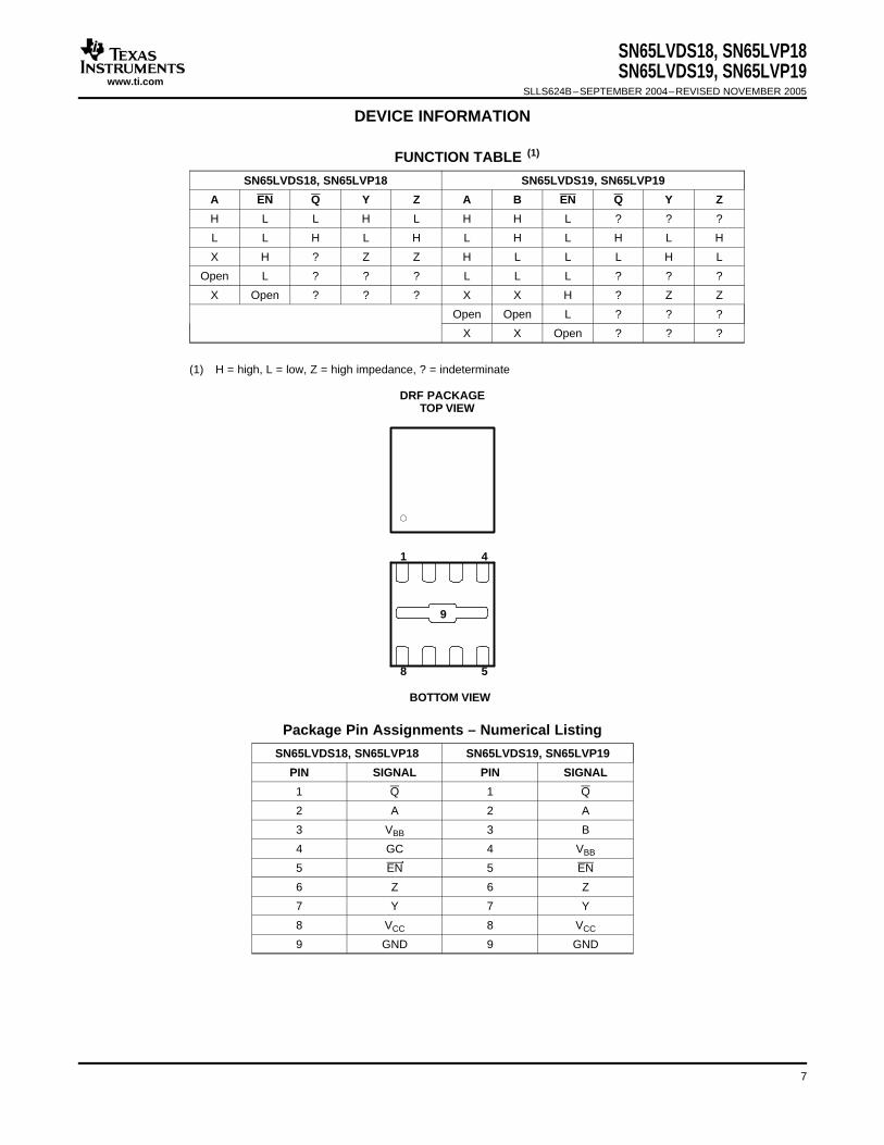
DEVICE INFORMATION
TOP VIEW
1 4
58
BOTTOM VIEW
9
SN65LVDS18, SN65LVP18SN65LVDS19, SN65LVP19
SLLS624B–SEPTEMBER 2004–REVISED NOVEMBER 2005
FUNCTION TABLE (1)
SN65LVDS18, SN65LVP18 SN65LVDS19, SN65LVP19
A EN Q Y Z A B EN Q Y Z
H L L H L H H L ? ? ?
L L H L H L H L H L H
X H ? Z Z H L L L H L
Open L ? ? ? L L L ? ? ?
X Open ? ? ? X X H ? Z Z
Open Open L ? ? ?
X X Open ? ? ?
(1) H = high, L = low, Z = high impedance, ? = indeterminate
DRF PACKAGE
Package Pin Assignments – Numerical Listing
SN65LVDS18, SN65LVP18 SN65LVDS19, SN65LVP19
PIN SIGNAL PIN SIGNAL
1 Q 1 Q
2 A 2 A
3 VBB 3 B
4 GC 4 VBB
5 EN 5 EN
6 Z 6 Z
7 Y 7 Y
8 VCC 8 VCC
9 GND 9 GND
7
www.ti.com
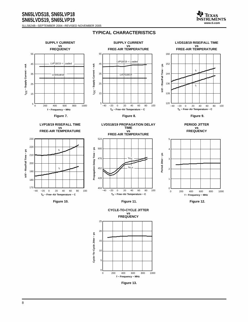
TYPICAL CHARACTERISTICS
120
128
136
144
152
160
−40 −20 0 20 40 60 80 100
tr/t
f −
Ris
e/F
all T
ime
− p
s
tr
tf
TA − Free−Air Temperature − C
5
15
25
35
45
55
0 200 400 600 800 1000
I CC
− S
up
ply
Cu
rren
t −
mA
f − Frequency − MHz
LVP18/19 = Loaded
LVDS18/19
5
15
25
35
45
55
−40 −20 0 20 40 60 80 100
I CC
− S
up
ply
Cu
rren
t −
mA
TA − Free−Air Temperature − C
LVP18/19 = Loaded
LVDS18/19
404
428
452
476
500
524
−40 −20 0 20 40 60 80 100
Pro
pag
atio
n D
elay
Tim
e −
ps
tPLH
tPHL
TA − Free−Air Temperature − C
170
180
190
200
210
220
230
−40 −20 0 20 40 60 80 100
tr/t
f −
Ris
e/F
all T
ime
− p
s
tr
tf
TA − Free−Air Temperature − C
0
1
2
3
4
5
0 200 400 600 800 1000
Per
iod
Jit
ter
− p
s
f − Frequency − MHz
0
5
10
15
20
25
0 200 400 600 800 1000
Cyc
le−T
o−C
ycle
Jit
ter
− p
s
f − Frequency − MHz
SN65LVDS18, SN65LVP18SN65LVDS19, SN65LVP19SLLS624B–SEPTEMBER 2004–REVISED NOVEMBER 2005
SUPPLY CURRENT SUPPLY CURRENT LVDS18/19 RISE/FALL TIMEvs vs vs
FREQUENCY FREE-AIR TEMPERATURE FREE-AIR TEMPERATURE
Figure 7. Figure 8. Figure 9.
LVP18/19 RISE/FALL TIME LVDS18/19 PROPAGATION DELAY PERIOD JITTERvs TIME vs
FREE-AIR TEMPERATURE vs FREQUENCYFREE-AIR TEMPERATURE
Figure 10. Figure 11. Figure 12.
CYCLE-TO-CYCLE JITTERvs
FREQUENCY
Figure 13.
8

www.ti.com
EQUIVALENT INPUT AND OUTPUT SCHEMATIC DIAGRAMS
R R
Y
Z
VCC
OUTPUT LVP18/19
VCC
VCC
7 V
7 V
VCC
Y Z
OUTPUT LVDS18/19
VCC
7 V7 V
VCC
VCC
300 kΩ
400 Ω
7 V
ENABLE
A B
VCC
INPUT
VCC
VBB
VCC VCC
VBBVBB
OUTPUT
SN65LVDS18, SN65LVP18SN65LVDS19, SN65LVP19
SLLS624B–SEPTEMBER 2004–REVISED NOVEMBER 2005
9
PACKAGE OPTION ADDENDUM
www.ti.com 10-Dec-2020
Addendum-Page 1
PACKAGING INFORMATION
Orderable Device Status(1)
Package Type PackageDrawing
Pins PackageQty
Eco Plan(2)
Lead finish/Ball material
(6)
MSL Peak Temp(3)
Op Temp (°C) Device Marking(4/5)
Samples
SN65LVDS18DRFT ACTIVE WSON DRF 8 250 RoHS & Green NIPDAU Level-1-260C-UNLIM -40 to 85 ER
SN65LVDS19DRFT ACTIVE WSON DRF 8 250 RoHS & Green NIPDAU Level-1-260C-UNLIM -40 to 85 ET
SN65LVP18DRFT ACTIVE WSON DRF 8 250 RoHS & Green NIPDAU Level-1-260C-UNLIM -40 to 85 EP
SN65LVP19DRFT ACTIVE WSON DRF 8 250 RoHS & Green NIPDAU Level-1-260C-UNLIM -40 to 85 ES
(1) The marketing status values are defined as follows:ACTIVE: Product device recommended for new designs.LIFEBUY: TI has announced that the device will be discontinued, and a lifetime-buy period is in effect.NRND: Not recommended for new designs. Device is in production to support existing customers, but TI does not recommend using this part in a new design.PREVIEW: Device has been announced but is not in production. Samples may or may not be available.OBSOLETE: TI has discontinued the production of the device.
(2) RoHS: TI defines "RoHS" to mean semiconductor products that are compliant with the current EU RoHS requirements for all 10 RoHS substances, including the requirement that RoHS substancedo not exceed 0.1% by weight in homogeneous materials. Where designed to be soldered at high temperatures, "RoHS" products are suitable for use in specified lead-free processes. TI mayreference these types of products as "Pb-Free".RoHS Exempt: TI defines "RoHS Exempt" to mean products that contain lead but are compliant with EU RoHS pursuant to a specific EU RoHS exemption.Green: TI defines "Green" to mean the content of Chlorine (Cl) and Bromine (Br) based flame retardants meet JS709B low halogen requirements of <=1000ppm threshold. Antimony trioxide basedflame retardants must also meet the <=1000ppm threshold requirement.
(3) MSL, Peak Temp. - The Moisture Sensitivity Level rating according to the JEDEC industry standard classifications, and peak solder temperature.
(4) There may be additional marking, which relates to the logo, the lot trace code information, or the environmental category on the device.
(5) Multiple Device Markings will be inside parentheses. Only one Device Marking contained in parentheses and separated by a "~" will appear on a device. If a line is indented then it is a continuationof the previous line and the two combined represent the entire Device Marking for that device.
(6) Lead finish/Ball material - Orderable Devices may have multiple material finish options. Finish options are separated by a vertical ruled line. Lead finish/Ball material values may wrap to twolines if the finish value exceeds the maximum column width.
Important Information and Disclaimer:The information provided on this page represents TI's knowledge and belief as of the date that it is provided. TI bases its knowledge and belief on informationprovided by third parties, and makes no representation or warranty as to the accuracy of such information. Efforts are underway to better integrate information from third parties. TI has taken and
PACKAGE OPTION ADDENDUM
www.ti.com 10-Dec-2020
Addendum-Page 2
continues to take reasonable steps to provide representative and accurate information but may not have conducted destructive testing or chemical analysis on incoming materials and chemicals.TI and TI suppliers consider certain information to be proprietary, and thus CAS numbers and other limited information may not be available for release.
In no event shall TI's liability arising out of such information exceed the total purchase price of the TI part(s) at issue in this document sold by TI to Customer on an annual basis.

TAPE AND REEL INFORMATION
*All dimensions are nominal
Device PackageType
PackageDrawing
Pins SPQ ReelDiameter
(mm)
ReelWidth
W1 (mm)
A0(mm)
B0(mm)
K0(mm)
P1(mm)
W(mm)
Pin1Quadrant
SN65LVDS18DRFT WSON DRF 8 250 330.0 8.8 2.3 2.3 1.0 4.0 8.0 Q2
SN65LVDS19DRFT WSON DRF 8 250 330.0 8.8 2.3 2.3 1.0 4.0 8.0 Q2
SN65LVP18DRFT WSON DRF 8 250 330.0 8.8 2.3 2.3 1.0 4.0 8.0 Q2
SN65LVP19DRFT WSON DRF 8 250 330.0 8.8 2.3 2.3 1.0 4.0 8.0 Q2
PACKAGE MATERIALS INFORMATION
www.ti.com 15-Sep-2018
Pack Materials-Page 1

*All dimensions are nominal
Device Package Type Package Drawing Pins SPQ Length (mm) Width (mm) Height (mm)
SN65LVDS18DRFT WSON DRF 8 250 337.0 343.0 29.0
SN65LVDS19DRFT WSON DRF 8 250 337.0 343.0 29.0
SN65LVP18DRFT WSON DRF 8 250 337.0 343.0 29.0
SN65LVP19DRFT WSON DRF 8 250 337.0 343.0 29.0
PACKAGE MATERIALS INFORMATION
www.ti.com 15-Sep-2018
Pack Materials-Page 2


IMPORTANT NOTICE AND DISCLAIMER
TI PROVIDES TECHNICAL AND RELIABILITY DATA (INCLUDING DATASHEETS), DESIGN RESOURCES (INCLUDING REFERENCE DESIGNS), APPLICATION OR OTHER DESIGN ADVICE, WEB TOOLS, SAFETY INFORMATION, AND OTHER RESOURCES “AS IS” AND WITH ALL FAULTS, AND DISCLAIMS ALL WARRANTIES, EXPRESS AND IMPLIED, INCLUDING WITHOUT LIMITATION ANY IMPLIED WARRANTIES OF MERCHANTABILITY, FITNESS FOR A PARTICULAR PURPOSE OR NON-INFRINGEMENT OF THIRD PARTY INTELLECTUAL PROPERTY RIGHTS.These resources are intended for skilled developers designing with TI products. You are solely responsible for (1) selecting the appropriate TI products for your application, (2) designing, validating and testing your application, and (3) ensuring your application meets applicable standards, and any other safety, security, or other requirements. These resources are subject to change without notice. TI grants you permission to use these resources only for development of an application that uses the TI products described in the resource. Other reproduction and display of these resources is prohibited. No license is granted to any other TI intellectual property right or to any third party intellectual property right. TI disclaims responsibility for, and you will fully indemnify TI and its representatives against, any claims, damages, costs, losses, and liabilities arising out of your use of these resources.TI’s products are provided subject to TI’s Terms of Sale (www.ti.com/legal/termsofsale.html) or other applicable terms available either on ti.com or provided in conjunction with such TI products. TI’s provision of these resources does not expand or otherwise alter TI’s applicable warranties or warranty disclaimers for TI products.
Mailing Address: Texas Instruments, Post Office Box 655303, Dallas, Texas 75265Copyright © 2020, Texas Instruments Incorporated