Embed Size (px)
Citation preview

24-Bit, 156 kSPS, 112 dB Sigma-Delta ADC with On-Chip Buffers and Serial Interface
Data Sheet AD7765
Rev. B Document Feedback Information furnished by Analog Devices is believed to be accurate and reliable. However, no responsibility is assumed by Analog Devices for its use, nor for any infringements of patents or other rights of third parties that may result from its use. Specifications subject to change without notice. No license is granted by implication or otherwise under any patent or patent rights of Analog Devices. Trademarks and registered trademarks are the property of their respective owners.
One Technology Way, P.O. Box 9106, Norwood, MA 02062-9106, U.S.A. Tel: 781.329.4700 ©2007–2018 Analog Devices, Inc. All rights reserved. Technical Support www.analog.com
FEATURES High performance 24-bit Σ-Δ ADC 115 dB dynamic range at 78.125 kHz output data rate 112 dB dynamic range at 156 kHz output data rate 156 kHz maximum fully filtered output word rate Pin-selectable oversampling rates of 128× and 256× Low power mode Flexible serial peripheral interface (SPI) Fully differential modulator input On-chip differential amplifier for signal buffering On-chip reference buffer Full band low-pass finite impulse response (FIR) filter Overrange alert pin Digital gain correction registers Power-down mode Synchronization of multiple devices via the SYNC pin Daisy chaining
APPLICATIONS Data acquisition systems Vibration analysis Instrumentation
FUNCTIONAL BLOCK DIAGRAM
REFGND
VREF+BUF
VOUTA– VOUTA+ VIN+ VIN– MCLK GND
OVERRANGE
DEC_RATE
AVDD1AVDD2AVDD3AVDD4DVDD
RBIAS
SYNC
RESET/PWRDWN
VINA+
VINA–
FSO SCO SDI SDO FSI
DIFF MULTIBITΣ-Δ
MODULATOR
RECONSTRUCTION
DECIMATION
FIR FILTER ENGINE
AD7765
INTERFACE LOGIC ANDOFFSET AND GAIN
CORRECTION REGISTERS
0651
9-00
1
Figure 1.
Table 1. Related Devices
Device No. Description AD7760 2.5 MSPS, 100 dB, parallel output, on-chip buffer AD7762 625 kSPS, 109 dB, parallel output, on-chip buffer AD7763 625 kSPS, 109 dB, serial output, on-chip buffers AD7765 312 kSPS, 109 dB, serial output, on-chip buffers AD7766 128 kSPS/64 kSPS/32 kSPS, 8.5 mW, 109 dB SNR AD7767 128 kSPS/64 kSPS/32 kSPS, 8.5 mW, 109 dB SNR
GENERAL DESCRIPTION The AD7765 is a high performance, 24-bit sigma-delta (Σ-Δ) analog-to-digital converter (ADC). It combines wide input bandwidth, high speed, and performance of 112 dB dynamic range at a 156 kHz output data rate. With excellent dc specifications, the converter is ideal for high speed data acquisition of ac signals where dc data is also required.
Using the AD7765 eases front-end antialias filtering requirements, simplifying the design process significantly. The AD7765 offers pin-selectable decimation rates of 128× and 256×. Other features include an integrated buffer to drive the reference, as well as a fully differential amplifier to buffer and level shift the input to the modulator.
An overrange alert pin indicates when an input signal exceeds the acceptable range. The addition of internal gain and internal overrange registers makes the AD7765 a compact, highly integrated data acquisition device requiring minimal peripheral components.
The AD7765 also offers a low power mode, significantly reducing power dissipation without reducing the output data rate or available input bandwidth.
The differential input is sampled at up to 40 MSPS by an analog modulator. The modulator output is processed by a series of low-pass filters. The external clock frequency applied to the AD7765 determines the sample rate, filter corner frequencies, and output word rate.
The AD7765 device boasts a full band on-board FIR filter. The full stop-band attenuation of the filter is achieved at the Nyquist frequency. This feature offers increased protection from signals that lie above the Nyquist frequency being aliased back into the input signal bandwidth.
The reference voltage supplied to the AD7765 determines the input range. With a 4 V reference, the analog input range is ±3.2768 V differential, biased around a common mode of 2.048 V. This common-mode biasing is achieved using the on-chip differential amplifier, further reducing the external signal conditioning requirements.
The AD7765 is available in a 28-lead TSSOP package and is specified over the industrial temperature range of −40°C to +85°C.

AD7765 Data Sheet
Rev. B | Page 2 of 34
TABLE OF CONTENTS Features .............................................................................................. 1 Applications ....................................................................................... 1 Functional Block Diagram .............................................................. 1 General Description ......................................................................... 1 Revision History ............................................................................... 2 Specifications ..................................................................................... 3
Timing Specifications .................................................................. 6 Absolute Maximum Ratings ............................................................ 8
ESD Caution .................................................................................. 8 Pin Configuration and Function Descriptions ............................. 9 Typical Performance Characteristics ........................................... 11 Terminology .................................................................................... 14 Theory of Operation ...................................................................... 15
Σ-Δ Modulation and Digital Filtering ..................................... 15 AD7765 Antialias Protection .................................................... 18
AD7765 Input Structure ................................................................ 19 On-Chip Differential Amplifier ............................................... 20 Modulator Input Structure ........................................................ 21 Driving the Modulator Inputs Directly ................................... 21
AD7765 Serial Interface ................................................................. 22 Reading Data ............................................................................... 22 Reading Status and Other Registers ......................................... 22 Writing to the AD7765 .............................................................. 22
Functionality ................................................................................... 23
Synchronization .......................................................................... 23 Overrange Alerts ........................................................................ 23 Power Modes ............................................................................... 24 Decimation Rate Pin .................................................................. 24
Daisy Chaining ............................................................................... 25 Reading Data in Daisy-Chain Mode........................................ 25 Writing Data in Daisy-Chain Mode ........................................ 26
Clocking the AD7765 .................................................................... 27 MCLK Jitter Requirements ....................................................... 27
Decoupling and Layout Information ........................................... 28 Supply Decoupling ..................................................................... 28 Reference Voltage Filtering ....................................................... 28 Differential Amplifier Components ........................................ 28 Layout Considerations ............................................................... 28 Using the AD7765 ...................................................................... 29 Bias Resistor Selection ............................................................... 29
AD7765 Registers ........................................................................... 30 Control Register ......................................................................... 30 Status Register ............................................................................. 30 Gain Register—Address 0x0004 ............................................... 31 Overrange Register—Address 0x0005 ..................................... 31
Outline Dimensions ....................................................................... 32 Ordering Guide .......................................................................... 32
REVISION HISTORY 1/2018—Rev. A to Rev. B Change to Features Section ............................................................. 1 Changes to Table 2 ............................................................................ 3 Changes to Table 3 ............................................................................ 6 Changes to Figure 3 Caption and Figure 4 Caption..................... 7 Changes to Table 4 ............................................................................ 8 Changes to Table 5 ............................................................................ 9 Changes to Terminology Section.................................................. 14 Added Table 6; Renumbered Sequentially .................................. 15 Changes to Σ-Δ Modulation and Digital Filtering Section ....... 15 Added Figure 27; Renumbered Sequentially .............................. 16 Added Table 8 and Table 9 ............................................................ 17 Changes to On-Chip Differential Amplifier Section and Table 10 ............................................................................................ 20 Changes to AD7765 Serial Interface Section Title, Reading Data Section, Table 12, and Table 13 Title .................................. 22 Changes to Overrange Alerts Section .......................................... 23 Changes to Table 14 ........................................................................ 24 Changes Daisy Chaining Section and Table 15 .......................... 25
Changes to MCLK Jitter Requirements Section ......................... 27 Changes to Layout Considerations Section and Figure 48 Caption ........................................................................... 28 Changes to Table 17 Endnote 2, Table 18, and Table 19 ............ 30 Changes to Ordering Guide .......................................................... 32 8/2009—Rev. 0 to Rev. A Changes to Table 3 ............................................................................. 6 Changes to Table 4 ............................................................................. 8 Changes to Σ-Δ Modulation and Digital Filtering Section ....... 15 Added AD7765 Antialias Protection Section ............................. 16 Added Driving the Modulator Inputs Directly Section ............ 19 Changes to Synchronization Section, Added Figure 35 ............ 21 Changes to Power Modes Section, Added RESET/PWRDWN Mode Section, Added Figure 38 ................................................... 22 Changes to Daisy Chaining Section ............................................. 23 Changes to Using the AD7765 Section........................................ 27
6/2007—Revision 0: Initial Version

Data Sheet AD7765
Rev. B | Page 3 of 34
SPECIFICATIONS AVDD1 = DVDD = 2.5 V, AVDD2 = AVDD3 = AVDD4 = 5 V, VREF+ = 4.096 V, MCLK amplitude = 5 V, TA = +25°C, normal power mode, using the on-chip amplifier with components as shown in the Optimal row in Table 10, unless otherwise noted.1
Table 2. Parameter Test Conditions/Comments Min Typ Max Unit DYNAMIC PERFORMANCE
Decimate 256× Normal Power Mode MCLK = 40 MHz, output data rate (ODR) =
78.125 kHz, fIN = 1 kHz sine wave
Dynamic Range Modulator inputs shorted 110 115 dB Differential amplifier inputs shorted 113.4 dB
Signal-to-Noise Ratio (SNR)2 Input amplitude = −0.5 dB 106 109 dB Spurious-Free Dynamic
Range (SFDR) Nonharmonic 130 dBFS
Total Harmonic Distortion (THD)
Input amplitude = −0.5 dB −105 dB
Input amplitude = −6 dB −103 dB Input amplitude = −60 dB −71 dB
Low Power Mode MCLK = 40 MHz, ODR = 78.125 kHz, fIN = 1 kHz sine wave
Dynamic Range Modulator inputs shorted 110 113 dB Differential amplifier inputs shorted 112 dB
SNR2 Input amplitude = −0.5 dB 106 109 dB THD Input amplitude = −0.5 dB −105 dB
Input amplitude = −6 dB −111 −100 dB Input amplitude = −60 dB −76 dB
Decimate 128× Normal Power Mode MCLK = 40 MHz, ODR = 156.25 kHz, fIN = 1 kHz
sine wave
Dynamic Range Modulator inputs shorted 108 112 dB Differential amplifier inputs shorted 110.4 dB SNR2 105 107 dB SFDR Nonharmonic 130 dBFS THD Input amplitude = −0.5 dB −105 dB Input amplitude = −6 dB −103 dB Intermodulation Distortion
(IMD) Input amplitude = −6 dB, fIN A = 50.3 kHz, fIN B = 47.3 kHz
Second-order terms −117 dB Third-order terms −108 dB
Low Power Mode MCLK = 40 MHz, ODR = 156.25 kHz, fIN = 1 kHz sine wave
Dynamic Range Modulator inputs shorted 109 110 dB Differential amplifier inputs shorted 109 dB SNR2 Input amplitude = −0.5 dB 105 107 dB THD Input amplitude = −0.5 dB −105 dB Input amplitude = −6 dB −111 dB Input amplitude = −6 dB −100 dB IMD Input amplitude = −6 dB, fIN A= 50.3 kHz, fIN B =
47.3 kHz
Second-order terms −134 dB Third-order terms −110 dB

AD7765 Data Sheet
Rev. B | Page 4 of 34
Parameter Test Conditions/Comments Min Typ Max Unit DC ACCURACY
Resolution Guaranteed monotonic to 24 bits 24 Bits Integral Nonlinearity Normal power mode 0.0036 % Low power mode 0.0014 % Zero Error Normal power mode 0.006 0.03 % Including on-chip amplifier 0.04 % Low power mode 0.002 0.024 % Gain Error 0.018 % Including on-chip amplifier 0.04 % Zero Error Drift Does not include on-chip amplifier 0.00006 %FS/°C Gain Error Drift Does not include on-chip amplifier 0.00005 %FS/°C
DIGITAL FILTER CHARACTERISTICS Normal and low power modes Pass-Band Ripple 0.1 dB Pass Band3 −1 dB frequency ODR ×
0.4016 kHz
−3 dB Bandwidth3 ODR × 0.4096
kHz
Stop Band3 Beginning of stop band ODR × 0.5 kHz Stop-Band Attenuation Decimate 128× −120 dB Decimate 256× −115 dB Group Delay See Table 8 and Table 9
ANALOG INPUT Differential Input Voltage Modulator input pins: VIN+ − VIN−, VREF+ = 4.096 V ±3.2768 V p-p Input Capacitance At on-chip differential amplifier inputs 5 pF
At modulator inputs 29 pF REFERENCE INPUT/OUTPUT
VREF+ Input Voltage AVDD3 = 5 V ± 5% 4.096 V VREF+ Input DC Leakage Current ±1 µA VREF+ Input Capacitance 5 pF
DIGITAL INPUT/OUTPUT MCLK Input Amplitude 2.25 5.25 V
Input Capacitance 7.3 pF Input Leakage Current ±1 μA/pin VINH 0.8 ×
DVDD V
VINL 0.2 × DVDD V VOH
4 2.2 V VOL 0.1 V
ON-CHIP DIFFERENTIAL AMPLIFIER Input Impedance >1 MΩ Bandwidth for 0.1 dB Flatness 125 kHz Common-Mode Input Voltage Common-mode voltage range at amplifier input
pins VINA− and VINA+ 0.8 +2.2 V
Common-Mode Output Voltage On-chip differential amplifier pins: VOUTA+ and VOUTA−
2.048 V
POWER REQUIREMENTS AVDD1 (Modulator Supply) 2.375 2.5 2.625 V AVDD2 (General Supply) 4.75 5 5.25 V AVDD3 (Differential Amplifier Supply)
5 V supply required for 4.096 V reference 3.15 5 5.25 V
AVDD4 (Reference Buffer Supply) 5 V supply required for 4.096 V reference 3.15 5 5.25 V DVDD 2.375 2.5 2.625 V

Data Sheet AD7765
Rev. B | Page 5 of 34
Parameter Test Conditions/Comments Min Typ Max Unit Normal Power Mode
AIDD1 (Modulator) 19 mA AIDD2 (General)5 MCLK = 40 MHz 13 mA AIDD3 (Differential Amplifier) AVDD3 = 5 V 10 mA AIDD4 (Reference Buffer) AVDD4 = 5 V 9 mA DIDD
5 MCLK = 40 MHz 37 mA Low Power Mode
AIDD1 (Modulator) 10 mA AIDD2 (General)5 MCLK = 40 MHz 7 mA AIDD3 (Differential Amplifier) AVDD3 = 5 V 5.5 mA AIDD4 (Reference Buffer) AVDD4 = 5 V 5 mA DIDD
5 MCLK = 40 MHz 20 mA POWER DISSIPATION
Normal Power Mode MCLK = 40 MHz, decimate 128× 300 371 mW Low Power Mode MCLK = 40 MHz, decimate 128× 160 215 mW Power-Down Mode6 PWRDWN pin held logic low 1 mW
1 See the Terminology section. 2 SNR specifications in decibels are referred to a full-scale input, FS, and are tested with an input signal at 0.5 dB below full scale, unless otherwise specified. 3 The output data rate (ODR) = [(MCLK/2)]/decimation rate. That is, the maximum ODR for AD7765 = [(40 MHz/2)/128] = 156.25 kHz. 4 Tested with a 400 µA load current. 5 Tested at MCLK = 40 MHz. This current scales linearly with the applied MCLK frequency. 6 Tested at 125°C.

AD7765 Data Sheet
Rev. B | Page 6 of 34
TIMING SPECIFICATIONS AVDD1 = DVDD = 2.5 V, AVDD2 = AVDD3 = AVDD4 = 5 V, VREF+ = 4.096 V, TA = 25°C, CLOAD = 25 pF.
Table 3.
Parameter Limit at TMIN, TMAX
Unit Description Min Typ Max fMCLK 500 kHz Applied master clock frequency 40 MHz fICLK 250 kHz Internal modulator clock derived from MCLK 20 MHz t1 1 × tICLK sec SCO high period t2 1 × tICLK sec SCO low period t3 1 2.5 ns SCO rising edge to FSO falling edge
t4 2 3.5 ns Data access time, FSO falling edge to data active
t5 8 ns MSB data access time, SDO active to SDO valid t6 40 ns Data hold time (SDO valid to SCO rising edge) t7 9.5 ns Data access time (SCO rising edge to SDO valid) t8 2 2.5 ns SCO rising edge to FSO rising edge
t9 32 × tSCO sec FSO low period
t10 12 ns Setup time from FSI falling edge to SCO falling edge
t11 1 × tSCO sec FSI low period
t121 32 × tSCO sec FSI low period
t13 12 ns SDI setup time for the first data bit t14 12 ns SDI setup time t15 0 ns SDI hold time tR MIN 1 × tMCLK sec Minimum time for a valid RESET pulse
tR HOLD 5 ns Minimum time between the MCLK rising edge and RESET rising edge
tR SETUP 5 ns Minimum time between the RESET rising edge and MCLK rising edge
tS MIN 4 × tMCLK sec Minimum time for a valid SYNC pulse
tS HOLD 5 ns Minimum time between the MCLK falling edge and SYNC rising edge
tS SETUP 5 ns Minimum time between the SYNC rising edge and MCLK falling edge 1 This is the maximum time FSI can be held low when writing to an individual device (a device that is not daisy-chained).

Data Sheet AD7765
Rev. B | Page 7 of 34
Timing Diagrams
D22D23 D21 D20 D19 D1 D0 ST4 ST3 ST2 ST1 ST0 0 0 0
SCO (O)
FSO (O)
SDO (O)
t1
t9
32 × tSCO
t2t8
t3
t4
t5 t7
t6
0651
9-00
2
Figure 2. Serial Read Timing Diagram
RA15 RA14 RA13 RA12 RA11 RA10 RA9 RA8 RA1 RA0 D15 D14 D1 D0
SCO (O)
FSI (I)
SDI (I)
t12
t1
t10
t13
t14
t15
t11
t2
0651
9-00
3
Figure 3. Register Write Timing Diagram
STATUS REGISTERCONTENTS [31:16]
DON’T CAREBITS [15:0]
SCO (O)
SDO (O)
FSI (I)
SDI (I)
FSO (O)
≥8 × tSCO
NEXT DATA READ FOLLOWING THE WRITE TO CONTROL REGISTER
CONTROL REGISTERADDR (0x0001)
CONTROL REGISTERINSTRUCTION
0651
9-00
4
Figure 4. Status Register Read Cycle Timing Diagram

AD7765 Data Sheet
Rev. B | Page 8 of 34
ABSOLUTE MAXIMUM RATINGSTA = 25°C, unless otherwise noted.
Table 4. Parameters Rating AVDD1 to Ground −0.3 V to +2.8 V AVDD2, AVDD3, AVDD4 to Ground −0.3 V to +6 V DVDD to Ground −0.3 V to +2.8 V VINA+, VINA− to Ground1 −0.3 V to +6 V VIN+, VIN− to Ground1 −0.3 V to +6 V Digital Input Voltage to Ground2 −0.3 V to +2.8 V VREF+ to Ground3 −0.3 V to +6 V Input Current to Any Pin Except Supplies4 ±10 mA Operating Temperature Range, Commercial −40°C to +85°C Storage Temperature Range −65°C to +150°C Junction Temperature 150°C θJA Thermal Impedance (1s0p)5 143°C/W θJA Thermal Impedance (2s2p)6, 7 71.1°C/W θJC
8 Thermal Impedance 20°C/W Lead Temperature, Soldering
Vapor Phase (60 sec) 215°C Infrared (15 sec) 220°C
ESD 1 kV
1 The absolute maximum voltage for VIN−, VIN+, VINA−, and VINA+ is 6.0 V or AVDD3 + 0.3 V, whichever is lower.
2 The absolute maximum voltage on the digital input is 3.0 V or DVDD + 0.3 V, whichever is lower.
3 The absolute maximum voltage on the VREF+ input is 6.0 V or AVDD4 + 0.3 V, whichever is lower.
4 Transient currents of up to 100 mA do not cause SCR latch-up. 5 1s0p means a single-layer printed circuit board (PCB), which includes
one signal layer and zero power layers. 6 2s2p means a 4-layer PCB, which includes two signal layers and two power layers. 7 θJA for a 2s2p PCB is derived from simulation. 8 The revised θJC (thermal impedance) is derived from simulation.
Stresses at or above those listed under Absolute Maximum Ratings may cause permanent damage to the product. This is a stress rating only; functional operation of the product at these or any other conditions above those indicated in the operational section of this specification is not implied. Operation beyond the maximum operating conditions for extended periods may affect product reliability.
ESD CAUTION

Data Sheet AD7765
Rev. B | Page 9 of 34
PIN CONFIGURATION AND FUNCTION DESCRIPTIONS 1
2
3
4
5
6
7
8
9
10
11
12
13
14
28
27
26
25
24
23
22
21
20
19
18
17
16
15
VOUTA+VINA+
VOUTA–
AVDD2VIN+VIN–
VINA–VREF+REFGNDAVDD4
RBIAS
AGND1AVDD1
AGND3OVERRANGE
SCO
FSI
SDOFSO
AVDD2AGND2MCLK
SYNCSDI RESET/PWRDWN
DVDD
DEC_RATE
AVDD3
AD7765TOP VIEW
(Not to Scale)
0651
9-00
5
Figure 5. Pin Configuration
Table 5. Pin Function Descriptions Pin No. Mnemonic Description 1 VINA− Negative Input to the Differential Amplifier. 2 VOUTA+ Positive Output from the Differential Amplifier. 3 VINA+ Positive Input to the Differential Amplifier. 4 VOUTA− Negative Output from the Differential Amplifier. 5 VIN− Negative Input to the Modulator. 6 VIN+ Positive Input to the Modulator. 7, 21 AVDD2 5 V Power Supply. Decouple Pin 7 to AGND3 (Pin 8) with a 100 nF capacitor. Decouple Pin 21 to AGND1
(Pin 23) with a 100 nF capacitor. 8 AGND3 Power Supply Ground for the Analog Circuitry. 9 OVERRANGE Overrange Pin. This pin outputs a logic high to indicate that the user applied an analog input that is approaching
the limit of the analog input to the modulator. 10 SCO Serial Clock Out. This clock signal is derived from the internal ICLK signal. The frequency of this clock is equal
to ICLK. See the Clocking the AD7765 section for more information. 11 FSO Frame Sync Out. This signal frames the serial data output and is 32 SCO periods wide.
12 SDO Serial Data Out. Data and status are output on this pin during each serial transfer. Each bit is clocked out on an SCO rising edge and is valid on the falling edge. See the AD7765 Serial Interface section for more information.
13 SDI Serial Data In. The first data bit (MSB) must be valid on the next SCO falling edge after the FSI event is latched. Thirty-two bits are required for each write; the first 16-bit word contains the device and register address, and the second word contains the data. See the AD7765 Serial Interface section for more information.
14 FSI Frame Sync Input. The status of this pin is checked on the falling edge of SCO. If this pin is low, then the first data bit is latched in on the next SCO falling edge. See the AD7765 Serial Interface section for more information.
15 SYNC Synchronization Input. A falling edge on this pin resets the internal filter. Use this pin to synchronize multiple devices in a system. See the Synchronization section for more information.
16 RESET/PWRDWN Reset/Power-Down Pin. When a logic low is sensed on this pin, the device is powered down and all internal circuitry is reset.
17 DVDD 2.5 V Power Supply for the Digital Circuitry and FIR Filter. Decouple this pin to the ground plane with a 100 nF capacitor.
18 DEC_RATE Decimation Rate Pin. This pin selects one of the three decimation rate modes. When 2.5 V is applied to this pin, a decimation rate of 128× is selected. Select a decimation rate of 256× by setting this pin to ground.
19 MCLK Master Clock Input. A low jitter digital clock must be applied to this pin. The output data rate depends on the frequency of this clock. See the Clocking the AD7765 section for more information.
20 AGND2 Power Supply Ground for the Analog Circuitry. 22 RBIAS Bias Current Setting Pin. This pin must be decoupled to the ground plane. For more information, see the Bias
Resistor Selection section.

AD7765 Data Sheet
Rev. B | Page 10 of 34
Pin No. Mnemonic Description 23 AGND1 Power Supply Ground for the Analog Circuitry. 24 AVDD1 2.5 V Power Supply for the Modulator. Decouple this pin to AGND1 (Pin 23) with a 100 nF capacitor. 25 AVDD4 3.3 V to 5 V Power Supply for the Reference Buffer. Decouple this pin to AGND1 (Pin 23) with a 100 nF capacitor. 26 REFGND Reference Ground. This pin is the ground connection for the reference voltage. 27 VREF+ Reference Input. 28 AVDD3 3.3 V to 5 V Power Supply for the Differential Amplifier. Decouple this pin to the ground plane with a 100 nF
capacitor.

Data Sheet AD7765
Rev. B | Page 11 of 34
TYPICAL PERFORMANCE CHARACTERISTICS AVDD1 = DVDD = 2.5 V, AVDD2 = AVDD3 = AVDD4 = 5 V, VREF+ = 4.096 V, MCLK amplitude = 5 V, TA = 25°C. Linearity plots measured to 16-bit accuracy; input signal reduced to avoid modulator overload and digital clipping; fast Fourier transforms (FFTs) generated from 8,192 samples.
0
–25
–50
–75
–100
–125
–150
–1750 25k 50k 75k
AM
PLIT
UD
E (d
B)
FREQUENCY (Hz) 0651
9-00
7
Figure 6. Normal Power Mode; FFT, 1 kHz, −0.5 dB Input Tone, 128× Decimation Rate
0
–25
–50
–75
–100
–125
–150
–1750 10k 20k 30k
AM
PLIT
UD
E (d
B)
FREQUENCY (Hz) 0651
9-00
8
Figure 7. Normal Power Mode; FFT, 1 kHz, −0.5 dB Input Tone, 256× Decimation Rate
0 50k 75k25k
AM
PLIT
UD
E (d
B)
FREQUENCY (Hz) 0651
9-20
1
0
–25
–50
–75
–100
–125
–150
–175
Figure 8. Normal Power Mode; FFT, 1 kHz, −6 dB Input Tone, 128× Decimation Rate
0 10k 20k 30k 40k 50k 60k 70k
AM
PLIT
UD
E (d
B)
FREQUENCY (Hz) 0651
9-21
1
0
–25
–50
–75
–100
–125
–150
–175
Figure 9. Low Power Mode; FFT, 1 kHz, −0.5 dB Input Tone, 128× Decimation Rate
0 5k 10k 15k 20k 25k 30k 35k
AM
PLIT
UD
E (d
B)
FREQUENCY (Hz) 0651
9-21
0
–15
–35
–55
–75
–95
–115
–135
–155
–175
Figure 10. Low Power Mode; FFT, 1 kHz, −0.5 dB Input Tone, 256× Decimation Rate
0 50k 75k25k
AM
PLIT
UD
E (d
B)
FREQUENCY (Hz) 0651
9-20
4
0
–25
–50
–75
–100
–125
–150
–175
Figure 11. Low Power Mode; FFT, 1 kHz, −6 dB Input Tone, 128× Decimation Rate

AD7765 Data Sheet
Rev. B | Page 12 of 34
0651
9-40
0
0 20k 30k10k
AM
PLIT
UD
E (d
B)
FREQUENCY (Hz)
0
–25
–50
–75
–100
–125
–150
–175
Figure 12. Normal Power Mode; FFT, 1 kHz, −6 dB Input Tone,
256× Decimation Rate
40
35
30
25
20
15
10
5
00 10 20 30 45405 15 25 35
CU
RR
ENT
(mA
)
MCLK FREQUENCY (MHz)
DVDD
AVDD2
AVDD3AVDD4
AVDD1
0651
9-11
4
Figure 13. Normal Power Mode; Current Consumption vs. MCLK Frequency,
128× Decimation Rate
40
35
30
25
20
15
10
5
00 10 20 30 405 15 25 35
CU
RR
ENT
(mA
)
MCLK FREQUENCY (MHz)
AVDD1
DVDD
AVDD2
AVDD3
AVDD4
0651
9-11
2
Figure 14. Normal Power Mode; Current Consumption vs. MCLK Frequency,
256× Decimation Rate
0 35k30k25k20k15k10k5k
AM
PLIT
UD
E (d
B)
FREQUENCY (Hz) 0651
9-20
5
0
–25
–50
–75
–100
–125
–150
–175
Figure 15. Low Power Mode; FFT, 1 kHz, −6 dB Input Tone,
256× Decimation Rate
25
20
15
10
5
00 10 20 30 45405 15 25 35
CU
RR
ENT
(mA
)
MCLK FREQUENCY (MHz)
DVDD
AVDD2
AVDD4
AVDD1
AVDD3
0651
9-11
5
Figure 16. Low Power Mode; Current Consumption vs. MCLK Frequency,
128× Decimation Rate
20
18
16
14
12
10
8
6
4
2
00 10 20 30 405 15 25 35
CU
RR
ENT
(mA
)
MCLK FREQUENCY (MHz)
DVDD
AVDD2
AVDD3
AVDD4
AVDD106
519-
113
Figure 17. Low Power Mode; Current Consumption vs. MCLK Frequency,
256× Decimation Rate

Data Sheet AD7765
Rev. B | Page 13 of 34
0.00300
–0.00300
–0.00225
–0.00150
–0.00075
0
0.00075
0.00150
0.00225
6k 55k 59,53510k 15k 20k 25k 30k 35k 40k 45k 50k
INL
(%)
16-BIT CODE SCALING
–40°C
+25°C
+85°C
0651
9-20
6
Figure 18. Normal Power Mode INL
0
–20
–40
–60
–80
–100
–120
–140
–160
–1800 78,12460k40k20k
AM
PLIT
UD
E (d
B)
FREQUENCY (Hz) 0651
9-20
9
Figure 19. Normal Power Mode; IMD, fIN A = 49.7 kHz, fIN B = 50.3 kHz, 50 kHz Center Frequency, 128× Decimation Rate
2.0
–2.0
–1.5
–1.0
–0.5
0
0.5
1.0
1.5
6k 55k 59,53510k 15k 20k 25k 30k 35k 40k 45k 50k
DN
L (L
SB)
CODE 0651
9-20
8
Figure 20. DNL Plot
6k 55k 59,53510k 15k 20k 25k 30k 35k 40k 45k 50k
INL
(%)
16-BIT CODE SCALING
–40°C
+25°C
+85°C
0651
9-20
7
0.0032250.003000
0.002250
0.001500
0.000075
0–0.000120
Figure 21. Low Power Mode INL
0651
9-00
9
110
109
108
107
106
105
104
103
1020 64 128 192 256
LOW SNR
SNR
(dB
)
DECIMATION RATE
NORMAL SNR
Figure 22. Normal and Low Power Mode; SNR vs. Decimation Rate, 1 kHz, −0.5 dB Input Tone

AD7765 Data Sheet
Rev. B | Page 14 of 34
TERMINOLOGY Signal-to-Noise Ratio (SNR) SNR is the ratio of the rms value of the actual input signal to the rms sum of all other spectral components below the Nyquist frequency, excluding harmonics and dc. The value for SNR is expressed in decibels (dB).
Total Harmonic Distortion (THD) THD is the ratio of the rms sum of the harmonics to the fundamental. For the AD7765, THD is defined as
THD (dB) = 20log 1
65432
V
VVVVV 22222 ++++
where: V2, V3, V4, V5, and V6 are the rms amplitudes of the second to the sixth harmonics. V1 is the rms amplitude of the fundamental.
Nonharmonic Spurious-Free Dynamic Range (SFDR) Nonharmonic SFDR is the ratio of the rms signal amplitude to the rms value of the peak spurious spectral component, excluding harmonics.
Dynamic Range Dynamic range is the ratio of the rms value of the full scale to the rms noise measured with the inputs shorted together. The value for dynamic range is expressed in decibels.
Intermodulation Distortion With inputs consisting of sine waves at two frequencies, fa and fb, any active device with nonlinearities creates distortion products at sum and difference frequencies of mfa ± nfb, where m, n = 0, 1, 2, 3, and so on. Intermodulation distortion terms are those for which neither m nor n is equal to 0. For example, the second-order terms include (fa + fb) and (fa − fb), while the third-order terms include (2fa + fb), (2fa − fb), (fa + 2fb), and (fa − 2fb).
The AD7765 is tested using the CCIF standard, where two input frequencies near the top end of the input bandwidth are used.
In this case, the second-order terms are typically distanced in frequency from the original sine waves, and the third-order terms are typically at a frequency close to the input frequencies. As a result, the second- and third-order terms are specified separately. The calculation of the intermodulation distortion is per the THD specification, where the calculation is the ratio of the rms sum of the individual distortion products to the rms amplitude of the sum of the fundamentals, expressed in decibels.
Integral Nonlinearity (INL) INL is the maximum deviation from a straight line passing through the endpoints of the ADC transfer function.
Differential Nonlinearity (DNL) DNL is the difference between the measured and the ideal 1 LSB change between any two adjacent codes in the ADC.
Zero Error Zero error is the difference between the ideal midscale input voltage (when both inputs are shorted together) and the actual voltage producing the midscale output code.
Zero Error Drift Zero error drift is the change in the actual zero error value due to a temperature change of 1°C. It is expressed as a percentage of full scale at room temperature.
Gain Error The first code transition (from 100 … 000 to 100 … 001) occurs for an analog voltage 1/2 LSB above the nominal negative full scale. The last code transition (from 011 … 110 to 011 … 111) occurs for an analog voltage 1 ½ LSB below the nominal full scale. The gain error is the deviation of the difference between the actual level of the last transition and the actual level of the first transition, from the difference between the ideal levels.
Gain Error Drift Gain error drift is the change in the actual gain error value due to a temperature change of 1°C. It is expressed as a percentage of full scale at room temperature.

Data Sheet AD7765
Rev. B | Page 15 of 34
THEORY OF OPERATION The AD7765 features an on-chip fully differential amplifier to feed the Σ-Δ modulator pins, an on-chip reference buffer, and a FIR filter block to perform the required digital filtering of the Σ-Δ modulator output. Using this Σ-Δ conversion technique with the added digital filtering, the analog input is converted to an equivalent digital word.
Σ-Δ MODULATION AND DIGITAL FILTERING The input waveform applied to the modulator is sampled, and an equivalent digital word is output to the digital filter at a rate equal to fICLK. By employing oversampling, the quantization noise is spread across a wide bandwidth from 0 to fICLK. This means that the noise energy contained in the signal band of interest is reduced (see Figure 23). To further reduce the quantization noise, a high-order modulator is employed to shape the noise spectrum so that most of the noise energy is shifted out of the signal band (see Figure 24).
QUANTIZATION NOISE
fICLK/2BAND OF INTEREST
0651
9-01
2
Figure 23. Σ-Δ ADC, Quantization Noise
fICLK/2
NOISE SHAPING
BAND OF INTEREST
0651
9-01
3
Figure 24. Σ-Δ ADC, Noise Shaping
fICLK/2BAND OF INTEREST
DIGITAL FILTER CUTOFF FREQUENCY
0651
9-01
4
Figure 25. Σ-Δ ADC, Digital Filter Cutoff Frequency
The modulator sampling rate, fICLK, is dependent on the power mode chosen. Table 6 details the relationship between MCLK and fICLK across power mode. The AD7765 low power mode divides the MCLK by a factor of 4, reducing current consumption in both the analog and digital domains.
Table 6. Modulator Sampling Rate vs. Power Mode Power Mode Modulator Sampling Rate (fICLK) Normal MCLK/2 Low MCLK/4
The digital filtering that follows the modulator removes the large out-of-band quantization noise (see Figure 25) while also reducing the data rate from fICLK at the input of the filter to fICLK /64 or less at the output of the filter, depending on the decimation rate used.
0
–160
–140
–120
–100
–80
–60
–40
–20
0 150125100755025
AM
PLIT
UD
E (d
B)
FREQUENCY (kHz)
PASS-BAND RIPPLE = 0.1dB–0.1dB FREQUENCY = 125.1kHz–3dB FREQUENCY = 128kHzSTOP BAND = 156.25kHz
0651
9-01
5
Figure 26. Filter Frequency Response
The AD7765 employs a sequence of three FIR filters in series to provide a digital filter with a low ripple pass band, a steep transition band, and excellent stop-band rejection, which starts at the Nyquist frequency. Achieving the stop-band rejection at the Nyquist frequency is beneficial because it prevents signals slightly greater than the Nyquist frequency, which are not protected by and external antialias filter from aliasing back in-band.
The AD7765 digital filter allows data to be output at three different output data rates (for any given MCLK input frequency) through setting the decimation ratio through the series of filters.
The first filter receives data from the modulator at fICLK MHz, where it is decimated 4× to the output data at (fICLK/4) MHz. The second filter allows the decimation rate to be chosen from 8× to 32×. The third filter has a fixed decimation rate of 2×.
Digital filters exhibit a group delay and settling time. The group delay of the filter is the delay from the change in analog input to when it is output by the digital filter. It is comprised of the comp-utation plus the filter delays. The delay until valid data is available (when the FILTER_SETTLE status bit is set) is approximately twice the filter delay plus the computation delay.

AD7765 Data Sheet
Rev. B | Page 16 of 34
The group delay and settling time of a digital filter is apparent in the behavior of the ADC response to a SYNC input pulse.
and Table 9 describe the response of the AD7765 in both normal and low power modes to a SYNC pulse, in addition to providing the group delay and settling times. Figure 27 shows the effect of SYNC and the subsequent signals from the AD7765.
The SYNC rising edge sets a known point in time from which the digital filter begins to process inputs from the modulator. This is useful in building a simultaneous sampling solution with multiple AD7765 devices, all clocked by the same MCLK.
The logic level of the SYNC pin is sampled by the rising edge of MCLK. Transitioning SYNC from low to high on an MCLK falling edge is recommended. Following the rising edge of SYNC, a number of MCLK periods pass before the first falling edge of FSO indicates a conversion output; this number of MCLK periods is defined as tSYNC OFFSET. Beyond tSYNC OFFSET, a number of conversion periods, each indicated by the falling edge of FSO, occur before the data from the filter is fully settled. During this time, outputs from the ADC have data that is a filtered mix of inputs to the modulator both before and after the time at which the SYNC signal transitioned from logic low to logic high.
All outputs from the ADC exhibit a group delay. The constant delay, due to the digital filter, is described by the number of conversion periods (tODR) that pass between a change occurring on the analog input being seen on the digital conversion output.
Figure 27 illustrates the group delay, showing a scenario where there is a step change on the analog inputs after the filter initially settles. As shown, a given number of periods of the output data rate occur before the digital output shows the step change.
Table 7. Group Delay (tGD_ODR) Expressed in Periods of the Output Data Rate
Decimation Rate
tGD_ODR in Output Data Rate Periods Normal Power Mode Low Power Mode
128× 28 28 256× 28 28
Because the group delay is not an exact number of conversion periods, a more precise way to describe the term is in MCLK periods. The exact region within a given conversion period where the analog input change occurs determines which output data period the ADC output responds to with a change in the digital output. Figure 27 shows that, if the step change on the input occurs at later point in time within the output period, the digital output remains updated within the same ODR period.
Described as the fine group delay, tGDMCLK, this delay consists of computation delay added to the actual delay through the filter provided in MCLK periods. Expressing the group delay in this manner allows it to be shown independent of the discrete steps of the ADC output data rate.
SYNC
MCLK
FSO
FILTERSETTLE
BIT
SDO(CONVERSION
RESULT)
ADCANALOGINPUTS
ADCANALOGOUTPUTS
tGDODR2
tGD MCLK1
1FINE GROUP DELAY IN tMLCK2COARSE GROUP DELAY IN tODR
tSYNC OFFSET
tSYNC_FS
0651
9-22
7
Figure 27. AD7765 Digital Filtering; Response to SYNC, Settling Time, and Group Delay

Data Sheet AD7765
Rev. B | Page 17 of 34
Table 8. Filter Group Delay and Settling Time in Normal Power Mode
Decimation Rate
Filter Computation Delay (tMCLK)
Filter Delay (tMCLK)
tGDMCLK ADC Group Delay (tMCLK)
tSYNC OFFSET (tMCLK)
tSYNC_FS
SYNC to FILTER_ SETTLE Bit (tMCLK)
Modulator Sampling Rate (fICLK)
Oversampling Ratio (OSR)
Filter Pass Band
Output Data Rate (ODR)
128× 113 6960 7073 141 13,966 MCLK/2 128 ODR × 0.4
MCLK/128
256× 443 13,608 14,051 252 27,901 MCLK/2 256 ODR × 0.4
MCLK/256
Table 9. Filter Group Delay and Settling Time for Low Power Mode
Decimation Rate
Filter Computation Delay (tMCLK)
Filter Delay (tMCLK)
tGDMCLK ADC Group Delay (tMCLK)
tSYNC OFFSET (tMCLK)
SYNC to FILTER_ SETTLE Bit (tMCLK)
Modulator Sampling Rate (fICLK)
Oversampling Ratio (OSR)
Filter Pass Band
Output Data Rate (ODR)
128× 162 7008 7170 167 14,248 MCLK/4 64 ODR × 0.4
MCLK/128
256× 224 13,920 14,144 277 27,926 MCLK/4 128 ODR × 0.4
MCLK/256
AD7765 Data Sheet
Rev. B | Page 18 of 34
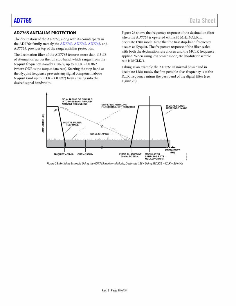
AD7765 ANTIALIAS PROTECTION The decimation of the AD7765, along with its counterparts in the AD776x family, namely the AD7760, AD7762, AD7763, and AD7765, provides top of the range antialias protection.
The decimation filter of the AD7765 features more than 115 dB of attenuation across the full stop band, which ranges from the Nyquist frequency, namely ODR/2, up to ICLK − ODR/2 (where ODR is the output data rate). Starting the stop band at the Nyquist frequency prevents any signal component above Nyquist (and up to ICLK − ODR/2) from aliasing into the desired signal bandwidth.
Figure 26 shows the frequency response of the decimation filter when the AD7765 is operated with a 40 MHz MCLK in decimate 128× mode. Note that the first stop-band frequency occurs at Nyquist. The frequency response of the filter scales with both the decimation rate chosen and the MCLK frequency applied. When using low power mode, the modulator sample rate is MCLK/4.
Taking as an example the AD7765 in normal power and in decimate 128× mode, the first possible alias frequency is at the ICLK frequency minus the pass band of the digital filter (see Figure 28).
NYQUIST = 78kHz ODR = 156kHz MODULATORSAMPLING RATE =MCLK/2 = 20MHz
FIRST ALIAS POINT20MHz TO 78kHz
SIMPLFIES ANTIALIASFILTER ROLL-OFF REQUIRED
DIGITAL FILTERRESPONSE
FREQUENCY(Hz)
DIGITAL FILTERRESPONSE IMAGE
NOISE SHAPING
AM
PLIT
UD
E (d
B)
NO ALIASING OF SIGNALSINTO PASSBAND AROUNDNYQUIST FREQUENCY
0651
9-30
0
Figure 28. Antialias Example Using the AD7765 in Normal Mode, Decimate 128× Using MCLK/2 = ICLK = 20 MHz

Data Sheet AD7765
Rev. B | Page 19 of 34
AD7765 INPUT STRUCTURE The AD7765 requires a 4.096 V input to the reference pin, VREF+, supplied by a high precision reference, such as the ADR444. Because the input to the Σ-Δ modulator of the device is fully differential, the effective differential reference range is 8.192 V.
VREF+ (Diff) = 2 × 4.096 = 8.192 V
As is inherent in Σ-Δ modulators, only a certain portion of this full reference can be used. With the AD7765, 80% of the full differential reference can be applied to the differential inputs of the modulator.
Modulator_InputFULL SCALE = 8.192 V × 0.8 = 6.5536 V
This means that a maximum of ±3.2768 V p-p full scale can be applied to each of the AD7765 modulator inputs (Pin 5 and Pin 6), with the AD7765 being specified with an input −0.5 dB down from full scale (−0.5 dBFS). The AD7765 modulator inputs must have a common-mode input of 2.048 V.
Figure 29 shows the relative scaling between the differential voltages applied to the modulator pins and the respective 24-bit, twos complement digital outputs.
INPUT TO MODULATORPIN 5 AND PIN 6
VIN– AND VIN+
VIN+ = 3.6855V 0111 1111 1111 1111 1111 1111
0000 0000 0000 0000 0000 0000
+3.2768V = MODULATOR FULL-SCALE = 80% OF 4.096V
80% OF 4.096V = MODULATOR FULL-SCALE = –3.2768V
+4.096V
–4.096V
VIN– = 0.4105V
VIN+ = 2.048VVIN– = 2.048V
VIN– = 3.6855VVIN+ = 0.4105V 1000 0000 0000 0000 0000 0000
0111 1000 1101 0110 1111 1101
1000 0111 0010 1001 0000 0010
–0.5dBFS INPUT
–0.5dBFS INPUT
OVERRANGE REGION
OVERRANGE REGION
DIGITAL OUTPUTON SDO PIN
0000 0000 0000 0000 0000 0001
1111 1111 1111 1111 1111 1111
TWOS COMPLEMENTDIGITAL OUTPUTINPUT VOLTAGE (V)
0651
9-12
0
Figure 29. AD7765 Scaling—Modulator Input Voltage vs. Digital Output Code

AD7765 Data Sheet
Rev. B | Page 20 of 34
ON-CHIP DIFFERENTIAL AMPLIFIER The AD7765 contains an on-board differential amplifier recommended to drive the modulator input pins. Pin 1, Pin 2, Pin 3, and Pin 4 on the AD7765 are the differential input and output pins of the amplifier. The external components, RIN, RFB, CFB, CS, and RM, are placed around Pin 1 through Pin 6 to create the recommended configuration.
To achieve the specified performance, configure the differential amplifier as a first-order antialias filter, as shown in Figure 30, using the component values listed in Table 10. The inputs to the differential amplifier are then routed through the external component network before being applied to the modulator inputs, VIN− and VIN+ (Pin 5 and Pin 6).
DIFFAMP
RINRFB
CFB
RIN
RM
RM
CS CM
RFB
CFB
VIN–A
B VIN+
0651
9-02
4
1
3
2
4
5
6
VINA–
VINA+
VOUTA+
VOUTA–
Figure 30. Differential Amplifier Configuration
Table 10. On-Chip Differential Filter Component Values
Value RIN (kΩ)
RFB
(kΩ) RM (Ω)
CS (pF)
CFB (pF)
CM (pF)
Optimal 4.75 3.01 43 8.2 47 33 Tolerance Range1
2.37 to 5.76
2.4 to 4.87
36 to 47
0 to 10
20 to 100
33 to 56
1 The values shown are the acceptable tolerances for each component when
altered relative to the optimal values that achieve the stated specifications of the device.
The range of values for each of the components in the differential amplifier configuration is listed in Table 10. When using the differential amplifier to gain the input voltages to the required modulator input range, it is recommended to implement the gain function by changing RIN and leaving RFB as the listed optimal value.
The common-mode input at each of the differential amplifier input pins (VINA+ and VINA−) can range from 0.8 V dc to 2.2 V dc. The amplifier has a constant output common-mode voltage of 2.048 V, that is, VREF/2, the requisite common-mode voltage for the modulator input pins (VIN+ and VIN−).
Figure 31 shows the signal conditioning that occurs using the differential amplifier configuration shown in Table 10 with a ±2.5 V input signal to the differential amplifier. The amplifier in this example is biased around ground and is scaled to provide ±3.0935 V p-p (−0.5 dBFS) on each modulator input with a 2.048 V common mode.
0V
+2.5V
–2.5V
0V
+2.5V
–2.5V
A
B
+3.632V
+2.048V
+0.464V
+3.632V
+2.048V
+0.464V
VIN+
VIN–
0651
9-12
2
Figure 31. Differential Amplifier Signal Conditioning
To obtain maximum performance from the AD7765, it is recommended to drive the ADC with differential signals. Figure 32 shows how a bipolar, single-ended signal biased around ground drives the AD7765 with the use of an external operational amplifier, such as the AD8021.
DIFFAMP
RIN RFB
CFB
RIN
RM
RM
CS
RFB
CFB
VIN–
VIN
VIN+
AD8021
2R
2R
RCM
0651
9-02
6
Figure 32. Single-Ended-to-Differential Conversion

Data Sheet AD7765
Rev. B | Page 21 of 34
MODULATOR INPUT STRUCTURE The AD7765 employs a double-sampling front end, as shown in Figure 33. For simplicity, only the equivalent input circuitry for VIN+ is shown. The equivalent circuitry for VIN− is the same.
CS2
CPB2SS4
SH4
CPA
SS2
SH2
CS1
CPB1SS3
SH3
SS1
SH1
ANALOGMODULATOR
VIN+
0651
9-02
7
Figure 33. Equivalent Input Circuit
The SS1 and SS3 sampling switches are driven by ICLK, whereas the SS2 and SS4 sampling switches are driven by ICLK. When ICLK is high, the analog input voltage is connected to CS1. On the falling edge of ICLK, the SS1 and SS3 switches open and the analog input is sampled on CS1. Similarly, when ICLK is low, the analog input voltage is connected to CS2. On the rising edge of ICLK, the SS2 and SS4 switches open, and the analog input is sampled on CS2.
The CPA, CPB1, and CPB2 capacitors represent parasitic capacitances that include the junction capacitances associated with the MOS switches.
Table 11. Equivalent Component Values CS1 (pF) CS2 (pF) CPA (pF) CPB1/CPB2 (pF) 13 13 13 5
DRIVING THE MODULATOR INPUTS DIRECTLY The AD7765 can be configured so that the on-board differential amplifier can be disabled and the modulator can be driven directly using discrete amplifiers. This allows the user to lower the power dissipation.
To power down the on board differential amplifier, the user issues a write to set the AMP OFF bit in the control register to logic high (see Figure 34). SCO (O)
CONTROL REGISTERADDRESS 0x0001
AMP OFF MODEDATA 0x0001
FSI (I)
SDI (I)
32 × tSCO
0651
9-30
1
Figure 34. Writing to the AD7765 Control Register Turning Off the On-Board
Differential Amplifier
The AD7765 modulator inputs must have a common-mode voltage of 2.048 V and adhere to the amplitudes as described in the AD7765 Input Structure section.
An example of a typical circuit to drive the AD7765 for applica-tions requiring excellent ac and dc performance is shown in Figure 35. Either the AD8606 or AD8656 can drive the AD7765 modulator inputs directly.
Best practice is to short the differential amplifier inputs to ground through the typical input resistors and leave the typical feedback resistors in place.
0651
9-30
2
1
VINA–
2
VOUTA+
RFB
RIN
3
VINA+
4
VOUTA–
RFB
RIN
6 VIN+
AD7764/AD7765
5
VIN–
U1
10kΩ
4.99kΩ
51Ω0Ω
10kΩ
C22
2.048V
U2
10kΩ
4.99kΩ51Ω0Ω
10kΩ
C12
1.024V AD8606AD8655
AD8606AD8655
ANALOGINPUT1
1–0.5dBFS INPUT SIGNAL AS DESCRIBED IN INPUT STRUCTURE SECTION.2SET C1 AND C2 AS REQUIRED FOR APPLICATION INPUT BW AND
ANTI-ALIAS REQUIREMENT. Figure 35. Driving the AD7765 Modulator Inputs Directly from a Single-
Ended Source (On-Board Differential Amplifier Powered Down)

AD7765 Data Sheet
Rev. B | Page 22 of 34
AD7765 SERIAL INTERFACE READING DATA The AD7765 uses a fully synchronous serial data interface where the ADC is the master providing frame, serial clock, and serial data outputs. The timing diagram in Figure 2 shows how the AD7765 transmits conversion results.
The data read from the AD7765 is clocked out using the serial clock output (SCO). The SCO frequency is half that of the MCLK input to the AD7765.
The conversion result output on the serial data output (SDO) line is framed by the frame synchronization output, FSO, which is sent logic low for 32 SCO cycles. Each bit of the new conversion result is clocked onto the SDO line on the rising SCO edge and is valid on the falling SCO edge. The 32-bit result consists of the 24 data bits followed by five status bits followed further by three zeros. The five status bits are listed in Table 12 and described in this section.
Table 12. Status Bits During a Data Read D7 D6 D5 D4 D3 FILTER-SETTLE OVR LPWR DEC_RATE 1 DEC_RATE 0
The FILTER-SETTLE bit indicates whether the data output from the AD7765 is valid. After resetting the device (using the RESET pin) or clearing the digital filter (using the SYNC pin), the FILTER_SETTLE bit goes logic low to indicate that the full settling time of the filter has not yet passed and that the data is not yet valid. The FILTER_SETTLE bit also goes to zero when the input to the device asserts the overrange alerts.
The OVR (overrange) bit is described in the Overrange Alerts section.
The LPWR bit is set to logic high when the AD7765 operates in low power mode. See the Power Modes section for further details.
The DEC_RATE 1 bit and the DEC_RATE 0 bit indicate the decimation ratio used. Table 13 is a truth table for the decimation rate bits.
Table 13. Decimation Rate Status Bits Decimate DEC_RATE 1 128× 1 256× 0
READING STATUS AND OTHER REGISTERS The AD7765 features a gain correction register, an overrange register, and a read-only status register. To read back the contents of these registers, the user must first write to the control register of the device and set the bit that corresponds to the register to be read. The next read operation outputs the contents of the selected register (on the SDO pin) instead of a conversion result.
To ensure that the next read cycle contains the contents of the register written to, the write operation to that register must be completed a minimum of 8 × tSCO before the falling edge of FSO, which indicates the start of the next read cycle. See Figure 4 for further details.
The AD7765 Registers section provides more information on the relevant bits in the control register.
WRITING TO THE AD7765 A write operation to the AD7765 is shown in Figure 3. The serial writing operation is synchronous to the SCO signal. The status of the frame synchronization input, FSI, is checked on the falling edge of the SCO signal. If the FSI line is low, then the first data bit on the serial data in (SDI) line is latched in on the next SCO falling edge.
Set the active edge of the FSI signal to occur at a position when the SCO signal is high or low to allow setup and hold times from the SCO falling edge to be met. The width of the FSI signal can be set to between 1 and 32 SCO periods wide. A second, or subsequent, falling edge that occurs before 32 SCO periods elapses is ignored.
Figure 3 details the format for the serial data being written to the AD7765 through the SDI pin. Thirty-two bits are required for a write operation. The first 16 bits select the register address that the data being read is intended for. The second 16 bits contain the data for the selected register.
Writing to the AD7765 is allowed at any time, even while reading a conversion result. Note that, after writing to the device, valid data is not output until after the settling time for the filter elapses. The FILTER_SETTLE status bit is asserted at this point to indicate that the filter has settled and that valid data is available at the output.

Data Sheet AD7765
Rev. B | Page 23 of 34
FUNCTIONALITY SYNCHRONIZATION
The SYNC input to the AD7765 provides a synchronization function that allows the user to begin gathering samples of the analog front-end input from a known point in time.
The SYNC function allows multiple AD7765 devices, operated from the same master clock that use common SYNC and RESET signals, to be synchronized so that each ADC simultaneously updates its output register. Note that all devices being synchronized must operate in the same power mode and at the same decimation rate.
In the case of a system with multiple AD7765 devices, connect common MCLK, SYNC, and RESET signals to each AD7765.
The AD7765 SYNC pin is polled by the falling edge of MCLK. The AD7765 device goes into SYNC when an MCLK falling edge senses that the SYNC input signal is logic low. At this point, the digital filter sequencer is reset to 0. The filter is held in a reset state (in SYNC mode) until the first MCLK falling edge senses SYNC to be logic high.
Where possible, ensure that all transitions of SYNC occur synchronously with the rising edge of MCLK (that is, as far away as possible from the MCLK falling edge, or decision edge). Otherwise, abide by the timing specified in Figure 36, which excludes the SYNC rising edge from occurring in a 10 ns window centered around the MCLK falling edge.
Keep SYNC logic low for a minimum of four MCLK periods. When the MCLK falling edge senses that SYNC has returned to logic high, the AD7765 filters begin to gather input samples simultaneously. The FSO falling edges are also synchronized, allowing for simultaneous output of conversion data.
0651
9-30
3
MCLK
SYNC
tS MIN4 × tMCLK tS HOLD
tS SETUP
Figure 36. SYNC Timing Relative to MCLK
Following a SYNC pulse, the digital filter needs time to settle before valid data can be read from the AD7765. To ensure there is valid data on the SDO line, Check the FILTER_SETTLE status bit (see D7 in Table 12) that is output with each conversion result. The time from the rising edge of SYNC until the FILTER_SETTLE bit asserts depends on the filter configuration used. See the Theory of Operation section and the values listed in Figure 6 for details on calculating the time until FILTER_SETTLE asserts.
Note that the FILTER_SETTLE bit is designed as a reactionary flag to indicate when the conversion data output is valid.
OVERRANGE ALERTS The AD7765 offers an overrange function in both a pin and status bit output. The overrange alerts indicate when the voltage applied to the AD7765 modulator input pins exceeds the limit set in the overrange register, indicating that the voltage applied is approaching a level that places the modulator in an overage condition. To set this limit, the user must program the register. The default overrange limit is set to 80% of the VREF voltage (see the AD7765 Registers section).
The OVERRANGE pin outputs logic high to alert the user that the modulator has sampled an input voltage greater in magnitude than the overrange limit as set in the overrange register. The OVERRANGE pin is set to logic high when the modulator samples an input above the overrange limit. After the input returns below the limit, the OVERRANGE pin returns to zero. The OVERRANGE pin is updated after the first FIR filter stage. The output of OVERRANGE changes at the ICLK/4 frequency.
The OVR status bit is output as Bit D6 on SDO during a data conversion and can be checked in the AD7765 status register. This bit is less dynamic than the OVERRANGE pin output. It is updated on each conversion result output; that is, the bit changes at the output data rate. If the modulator samples a voltage input that exceeds the overrange limit during the process of gathering samples for a particular conversion result output, then the OVR bit is set to logic high.
OVE
RR
AN
GE
PIN
OU
TPU
T
LOGICLEVEL
HIGH
LOW
OVR
BIT
LOGICLEVEL
HIGH
LOW
OUTPUT FREQUENCYOF FIR FILTER 1 = ICLK/4
OVERRANGELIMIT
OVERRANGELIMIT
ABSOLUTE INPUTTO AD7765[(VIN+) – (VIN–)]
OUTPUT DATA RATE (ODR)(ICLK/DECIMATION RATE
t
t
0651
9-01
6
Figure 37. OVERRANGE Pin and OVR Bit vs. Absolute Voltage
Applied to the Modulator
The output points from FIR Filter 1 in Figure 37 are not drawn to scale relative to the output data rate points. The FIR Filter 1 output is updated either 16×, 32×, or 64× faster than the output data rate, depending on the decimation rate in operation.

AD7765 Data Sheet
Rev. B | Page 24 of 34
POWER MODES Low Power Mode
During power-up, the AD7765 defaults to operate in normal power mode. There is no register write required.
The AD7765 also offers low power mode. To operate the device in low power mode, set the LPWR bit in the control register to logic high (see Figure 38). Operating the AD7765 in low power mode has no impact on the output data rate or available bandwidth. SCO (O)
CONTROL REGISTERADDRESS 0x0001
LOW POWER MODEDATA 0x0004
FSI (I)
SDI (I)
32 × tSCO
0651
9-01
7
Figure 38. Write Scheme for Low Power Mode
RESET/PWRDWN Mode
The AD7765 features a RESET/PWRDWN pin. Holding the input to this pin logic low places the AD7765 in power-down mode. All internal circuitry is reset. Apply a RESET pulse to the AD7765 after initial power-up of the device.
The AD7765 RESET pin is polled by the rising edge of MCLK. The AD7765 device goes into reset when an MCLK rising senses the RESET input signal to be logic low. AD7765 comes out of RESET on the first MCLK rising edge that senses RESET to be logic high.
The best practice is to ensure that all transitions of RESET occur synchronously with the falling edge of MCLK; otherwise, adhere to the timing requirements shown in Figure 39.
Keep RESET at logic low for a minimum of one MCLK period for a valid reset to occur.
In cases where multiple AD7765 devices are being synchronized using the SYNC pulse and in the case of daisy chaining multiple AD7765 devices, a common RESET pulse must be provided in addition to the common SYNC and MCLK signals.
0651
9-30
4
MCLK
tR MIN1 × tMCLK tR HOLD
tR SETUP
RESET
Figure 39. RESET Timing Synchronous to MCLK
DECIMATION RATE PIN The decimation rate of the AD7765 is selected using the DEC_RATE pin. Table 14 shows the voltage input settings required for each of the three decimation rates.
Table 14. DEC_RATE Pin Settings
Decimation Rate DEC_RATE Pin State Maximum ODR (kHz)
128× DVDD 156.25 256× Ground 78.125

Data Sheet AD7765
Rev. B | Page 25 of 34
DAISY CHAINING Daisy chaining allows numerous devices to use the same digital interface lines. This feature is especially useful for reducing component count and wiring connections, such as in isolated multiconverter applications or for systems with a limited inter-facing capacity. Data readback is analogous to clocking a shift register. When daisy chaining is used, all devices in the chain must operate in a common power mode and at a common decimation rate.
The block diagram in Figure 40 shows how to connect devices to achieve daisy-chain functionality. Figure 40 shows four AD7765 devices daisy-chained together with a common MCLK signal applied. This configuration works in decimate 128× or decimate 256× mode only.
READING DATA IN DAISY-CHAIN MODE Referring to Figure 40, note that the SDO line of AD7765 (A) provides the output data from the chain of AD7765 converters. Also, note that for the last device in the chain, AD7765 (D), the SDI pin is connected to ground. All of the devices in the chain must use common MCLK and SYNC signals.
To enable the daisy-chain conversion process, apply a common SYNC pulse to all devices (see the Synchronization section).
After a SYNC pulse is applied to all devices, the filter settling time must pass before the FILTER_SETTLE bit is asserted indicating valid conversion data at the output of the chain of devices. As shown in Figure 41, the first conversion result is
output from the device labeled AD7765 (A). This 32-bit conversion result is then followed by the conversion results from the AD7765 (B), AD7765 (C), and AD7765 (D) devices with all conversion results output in an MSB-first sequence. The signals output from the daisy chain are the stream of conversion results from the SDO pin of AD7765 (A) and the FSO signal output by the first device in the chain, AD7765 (A).
The falling edge of FSO signals the MSB of the first conversion output in the chain. FSO stays logic low throughout the 32 SCO clock periods needed to output the AD7765 (A) result and then goes logic high during the output of the conversion results from the AD7765 (B), AD7765 (C), and AD7765 (D) devices.
The maximum number of devices that can be daisy-chained is dependent on the decimation rate selected. Calculate the maximum number of devices that can be daisy-chained by simply dividing the chosen decimation rate by 32 (the number of bits that must be clocked out for each conversion). Table 15 provides the maximum number of chained devices for each decimation rate.
Table 15. Maximum Daisy Chain Length for all Decimation Rates Decimation Rate Maximum Chain Length 256× 8 devices 128× 4 devices
SYNC
SDI
FSI
SDO
MCLK
AD7765(D)
FSI
SYNC
MCLK
SYNC
SDI
FSI
SDO
MCLK
AD7765(C)
SYNC
SDI
FSI
SDO
MCLK
AD7765(B)
SYNC
SDI
FSI
MCLK
AD7765(A)
SDO
FSO
0651
9-01
8
Figure 40. Daisy Chaining Four Devices in Decimate 128× Mode Using a 40 MHz MCLK Signal
SCO
FSO (A)
32 × tSCO 32 × tSCO 32 × tSCO 32 × tSCO
SDO (A) AD7765 (A)32-BIT OUTPUT
AD7765 (B)32-BIT OUTPUT
AD7765 (C)32-BIT OUTPUT
AD7765 (D)32-BIT OUTPUT
AD7765 (A)32-BIT OUTPUT
AD7765 (B)32-BIT OUTPUT
SDI (A) = SDO (B) AD7765 (B) AD7765 (C) AD7765 (D) AD7765 (B) AD7765 (C)
SDI (B) = SDO (C) AD7765 (C) AD7765 (D) AD7765 (C) AD7765 (D)
SDI (C) = SDO (D) AD7765 (D) AD7765 (D)
0651
9-01
9
Figure 41. Daisy-Chain Mode, Data Read Timing Diagram
(for the Daisy-Chain Configuration Shown in Figure 40)

AD7765 Data Sheet
Rev. B | Page 26 of 34
WRITING DATA IN DAISY-CHAIN MODE Writing to AD7765 devices in daisy-chain mode is similar to writing to a single device. The serial writing operation is synch-ronous to the SCO signal. The status of the frame synchronization input, FSI, is checked on the falling edge of the SCO signal. If the FSI line is low, then the first data bit on the serial data in the SDI line is latched in on the next SCO falling edge.
Writing data to the AD7765 in daisy-chain mode operates with the same timing structure as writing to a single device (see Figure 3). The difference between writing to a single device and writing to a number of daisy-chained devices is in the implementation of the FSI signal. The number of devices that are in the daisy chain determines the period for which the FSI signal must remain logic low. To write to n number of devices in the daisy chain, the period between the falling edge of FSI and the rising edge of FSI must be between 32 × (n − 1) to 32 × n SCO periods.
For example, if three AD7765 devices are being written to in daisy-chain mode, FSI is logic low for between 32 × (3 − 1) to 32 × 3 SCO pulses. This means that the rising edge of FSI must occur between the 64th and 96th SCO periods.
The AD7765 devices can be written to at any time. The falling edge of FSI overrides all attempts to read data from the SDO pin. In the case of a daisy chain, the FSI signal remaining logic low for more than 32 SCO periods indicates to the AD7765 device that there are more devices further on in the chain. This means that the AD7765 directs data that is input on the SDI pin to its SDO pin. This ensures that data is passed to the next device in the chain.
SYNC
SDI
FSI
SDO
MCLK
AD7765(D)
FSI
SYNC
MCLK
SYNC
SDI
FSI
SDO
MCLK
AD7765(C)
SYNC
SDI
FSI
SDO
MCLK
AD7765(B)
SYNC
SDI
FSI
MCLK
AD7765(A)
SDO
FSO
SDI
0651
9-02
0
Figure 42. Writing to an AD7765 Daisy-Chain Configuration
FSI
SCO
SDI (D)
SDI (C) = SDO (D)
SDI (B) = SDO (C)
SDI (A) = SDO (B)
SDI (D)
SDI (C)
SDI (B)
SDI (A)
32 × tSCO 32 × tSCO 32 × tSCO 31 × tSCO
t10
0651
9-02
1
Figure 43. Daisy-Chain Write Timing Diagram; Writing to Four AD7765 Devices

Data Sheet AD7765
Rev. B | Page 27 of 34
CLOCKING THE AD7765 The AD7765 requires an external low jitter clock source. This signal is applied to the MCLK pin. An internal clock signal (ICLK) is derived from the MCLK input signal. The ICLK controls the internal operation of the AD7765. The maximum ICLK frequency is 20 MHz. To generate the ICLK,
ICLK = MCLK/2
For output data rates equal to those used in audio systems, a 12.288 MHz ICLK frequency can be used. As shown in Table 6, output data rates of 96 kHz and 48 kHz are achievable with this ICLK frequency.
MCLK JITTER REQUIREMENTS The MCLK jitter requirements depend on a number of factors and are given by
20)(
102)( dBSNR
f
OSRtIN
rmsj
××π×=
where: tj(rms) is rms jitter. OSR (the oversampling ratio) = fICLK/ODR. fIN is the maximum input frequency. SNR (dB) is the target SNR.
Example 1
Take Example 1 from Table 6, where: ODR = 156.25 kHz. fICLK = 20 MHz. fIN (max) = 78.625 kHz. SNR = 104 dB.
ps29.1021010625.782
12835.53)( =
×××π×=rmsjt
This is the maximum allowable clock jitter for a full-scale, 78.625 kHz input tone with the given ICLK and output data rate.
Example 2
Take Example 2 from Table 6, where: ODR = 48 kHz. fICLK = 12.288 MHz. fIN (max) = 19.2 kHz. SNR = 109 dB.
ps47010102.192
25645.53)( =
×××π×=rmsjt
The input amplitude also has an effect on these jitter figures. For example, if the input level is 3 dB below full scale, the allowable jitter is increased by a factor of √2, increasing the first example to 144.65 ps rms. This happens when the maximum slew rate is decreased by a reduction in amplitude.
Figure 44 and Figure 45 illustrate this point, showing the maximum slew rate of a sine wave of the same frequency but with different amplitudes.
1.0
–1.0
0.5
0
–0.5
0651
9-02
2
Figure 44. Maximum Slew Rate of a Sine Wave
with an Amplitude of 2 V p-p
1.0
–1.0
0.5
0
–0.5
0651
9-02
3
Figure 45. Maximum Slew Rate of the Same Frequency Sine Wave as in
Figure 44 with an Amplitude of 1 V p-p
AD7765 Data Sheet
Rev. B | Page 28 of 34
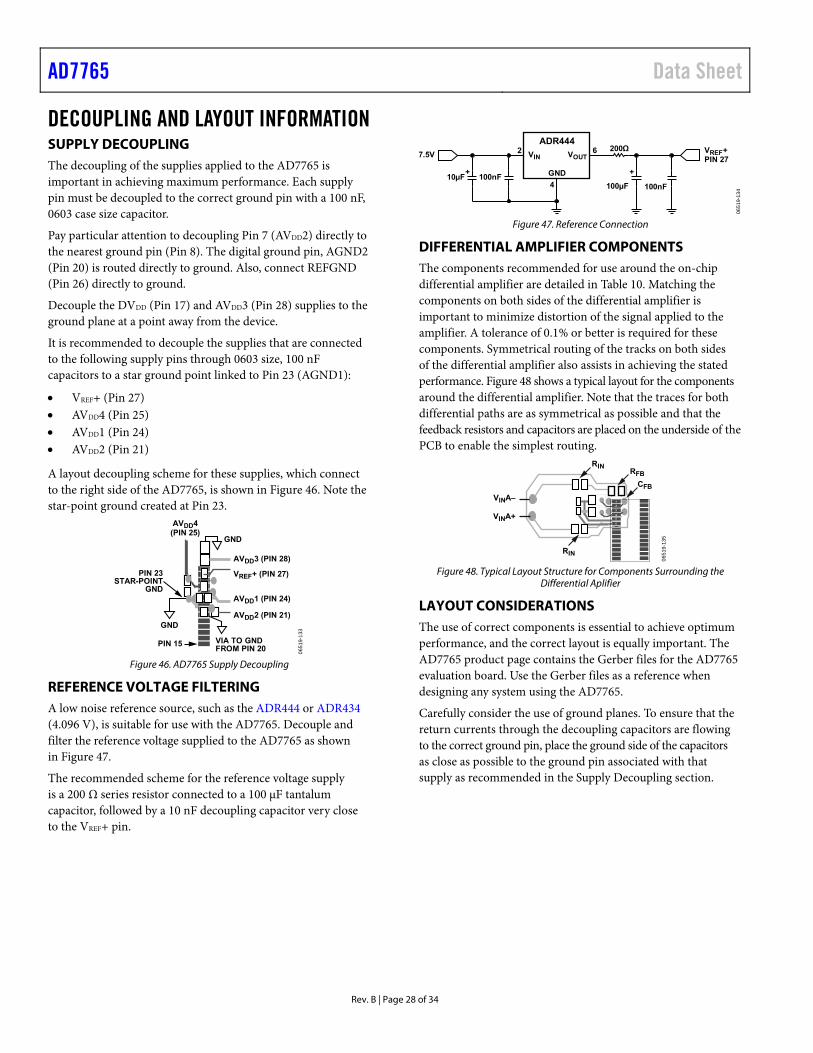
DECOUPLING AND LAYOUT INFORMATION SUPPLY DECOUPLING The decoupling of the supplies applied to the AD7765 is important in achieving maximum performance. Each supply pin must be decoupled to the correct ground pin with a 100 nF, 0603 case size capacitor.
Pay particular attention to decoupling Pin 7 (AVDD2) directly to the nearest ground pin (Pin 8). The digital ground pin, AGND2 (Pin 20) is routed directly to ground. Also, connect REFGND (Pin 26) directly to ground.
Decouple the DVDD (Pin 17) and AVDD3 (Pin 28) supplies to the ground plane at a point away from the device.
It is recommended to decouple the supplies that are connected to the following supply pins through 0603 size, 100 nF capacitors to a star ground point linked to Pin 23 (AGND1):
VREF+ (Pin 27) AVDD4 (Pin 25) AVDD1 (Pin 24) AVDD2 (Pin 21)
A layout decoupling scheme for these supplies, which connect to the right side of the AD7765, is shown in Figure 46. Note the star-point ground created at Pin 23.
AVDD2 (PIN 21)
VREF+ (PIN 27)
GND
PIN 23STAR-POINT
GND
AVDD4(PIN 25)
AVDD3 (PIN 28)
VIA TO GNDFROM PIN 20
AVDD1 (PIN 24)
GND
PIN 15
0651
9-13
3
Figure 46. AD7765 Supply Decoupling
REFERENCE VOLTAGE FILTERING A low noise reference source, such as the ADR444 or ADR434 (4.096 V), is suitable for use with the AD7765. Decouple and filter the reference voltage supplied to the AD7765 as shown in Figure 47.
The recommended scheme for the reference voltage supply is a 200 Ω series resistor connected to a 100 μF tantalum capacitor, followed by a 10 nF decoupling capacitor very close to the VREF+ pin.
7.5V VOUT2 VIN
6
410µF 100nF
+
100nF
+
ADR444
GND
VREF+PIN 27
100µF
200Ω
0651
9-13
4
Figure 47. Reference Connection
DIFFERENTIAL AMPLIFIER COMPONENTS The components recommended for use around the on-chip differential amplifier are detailed in Table 10. Matching the components on both sides of the differential amplifier is important to minimize distortion of the signal applied to the amplifier. A tolerance of 0.1% or better is required for these components. Symmetrical routing of the tracks on both sides of the differential amplifier also assists in achieving the stated performance. Figure 48 shows a typical layout for the components around the differential amplifier. Note that the traces for both differential paths are as symmetrical as possible and that the feedback resistors and capacitors are placed on the underside of the PCB to enable the simplest routing.
RFB
CFB
RIN
RIN
VINA–
VINA+
0651
9-13
5
Figure 48. Typical Layout Structure for Components Surrounding the
Differential Aplifier
LAYOUT CONSIDERATIONS The use of correct components is essential to achieve optimum performance, and the correct layout is equally important. The AD7765 product page contains the Gerber files for the AD7765 evaluation board. Use the Gerber files as a reference when designing any system using the AD7765.
Carefully consider the use of ground planes. To ensure that the return currents through the decoupling capacitors are flowing to the correct ground pin, place the ground side of the capacitors as close as possible to the ground pin associated with that supply as recommended in the Supply Decoupling section.

Data Sheet AD7765
Rev. B | Page 29 of 34
USING THE AD7765 Use the following to power up and use the AD7765:
1. Apply power to the device. 2. Apply the MCLK signal. 3. Take RESET low for a minimum of one MCLK cycle,
preferably synchronous to the falling MCLK edge. If multiple devices are to be synchronized, apply a common RESET to all devices.
4. Wait a minimum of two MCLK cycles after RESET is released.
5. If multiple devices are being synchronized, a SYNC pulse must be applied to the devices, preferably synchronous with the MCLK rising edge. In the case where devices are not being synchronized, no SYNC pulse is required; apply a logic high signal to the SYNC pin.
When applying the SYNC pulse,
• The issue of a SYNC pulse to the device must not coincide with a write to the device.
• Ensure that the SYNC pulse is taken low for a minimum of four MCLK periods.
Data can then be read from the device using the default gain and overrange threshold values. The conversion data read is not valid, however, until the settling time of the filter elapses. After time elapses, the FILTER_SETTLE status bit is set, indicating that the data is valid.
Values for the gain and overrange thresholds can be written to or read from the respective registers at this stage.
BIAS RESISTOR SELECTION The AD7765 requires a resistor to be connected between the RBIAS and AGNDx pins. Select the resistor value to give a current of 25 µA through the resistor to ground. For a 4.096 V reference voltage, the correct resistor value is 160 kΩ.
AD7765 Data Sheet
Rev. B | Page 30 of 34
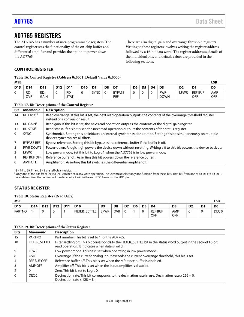
AD7765 REGISTERS The AD7765 has a number of user-programmable registers. The control register sets the functionality of the on-chip buffer and differential amplifier and provides the option to power down the AD7765.
There are also digital gain and overrange threshold registers. Writing to these registers involves writing the register address followed by a 16-bit data word. The register addresses, details of the individual bits, and default values are provided in the following sections.
CONTROL REGISTER
Table 16. Control Register (Address 0x0001, Default Value 0x0000) MSB LSB D15 D14 D13 D12 D11 D10 D9 D8 D7 D6 D5 D4 D3 D2 D1 D0 0 RD
OVR RD GAIN
0 RD STAT
0 SYNC 0 BYPASS REF
0 0 0 PWR DOWN
LPWR REF BUF OFF
AMP OFF
Table 17. Bit Descriptions of the Control Register Bit Mnemonic Description 14 RD OVR1, 2 Read overrange. If this bit is set, the next read operation outputs the contents of the overrange threshold register
instead of a conversion result. 13 RD GAIN2 Read gain. If this bit is set, the next read operation outputs the contents of the digital gain register. 11 RD STAT2 Read status. If this bit is set, the next read operation outputs the contents of the status register. 9 SYNC1 Synchronize. Setting this bit initiates an internal synchronization routine. Setting this bit simultaneously on multiple
devices synchronizes all filters. 7 BYPASS REF Bypass reference. Setting this bit bypasses the reference buffer if the buffer is off. 3 PWR DOWN Power-down. A logic high powers the device down without resetting. Writing a 0 to this bit powers the device back up. 2 LPWR Low power mode. Set this bit to Logic 1 when the AD7765 is in low power mode. 1 REF BUF OFF Reference buffer off. Asserting this bit powers down the reference buffer. 0 AMP OFF Amplifier off. Asserting this bit switches the differential amplifier off.
1 Bit 14 to Bit 11 and Bit 9 are self-clearing bits. 2 Only one of the bits from D14 to D11 can be set in any write operation. The user must select only one function from these bits. That bit, from one of Bit D14 to Bit D11,
read determines the contents of the data output within the next FSO frame on the SDO pin.
STATUS REGISTER
Table 18. Status Register (Read Only) MSB LSB D15 D14 D13 D12 D11 D10 D9 D8 D7 D6 D5 D4 D3 D2 D1 D0 PARTNO 1 0 0 1 FILTER_SETTLE LPWR OVR 0 1 0 REF BUF
OFF AMP OFF
0 0 DEC 0
Table 19. Bit Descriptions of the Status Register Bits Mnemonic Description 15 PARTNO Part number. This bit is set to 1 for the AD7765. 10 FILTER_SETTLE Filter settling bit. This bit corresponds to the FILTER_SETTLE bit in the status word output in the second 16-bit
read operation. It indicates when data is valid. 9 LPWR Low power mode. This bit is set when operating in low power mode. 8 OVR Overrange. If the current analog input exceeds the current overrange threshold, this bit is set. 4 REF BUF OFF Reference buffer off. This bit is set when the reference buffer is disabled. 3 AMP OFF Amplifier off. This bit is set when the input amplifier is disabled. 2 0 Zero. This bit is set to Logic 0. 0 DEC 0 Decimation rate. This bit corresponds to the decimation rate in use. Decimation rate x 256 = 0,
Decimation rate x 128 = 1.

Data Sheet AD7765
Rev. B | Page 31 of 34
GAIN REGISTER—ADDRESS 0x0004 Nonbit Mapped, Default Value: 0xA000
The gain register is scaled such that 0x8000 corresponds to a gain of 1.0. The default value of this register is 1.25 (0xA000). This value results in a full-scale digital output when the input is at 80% of VREF+, tying in with the maximum analog input range of ±80% of VREF+ p-p.
OVERRANGE REGISTER—ADDRESS 0x0005 Nonbit Mapped, Default Value: 0xCCCC
The overrange register value is compared to the output of the first decimation filter to obtain an overload indication with minimum propagation delay. This comparison is prior to any gain scaling. The default value is 0xCCCC, which corresponds to 80% of VREF+ (the maximum permitted analog input voltage). Assuming VREF+ = 4.096 V, the bit is then set when the input voltage exceeds approximately 6.55 V p-p differential. The over-range bit is set immediately if the analog input voltage exceeds 100% of VREF+ for more than four consecutive samples at the modulator rate.

AD7765 Data Sheet
Rev. B | Page 32 of 34
OUTLINE DIMENSIONS
COMPLIANT TO JEDEC STANDARDS MO-153-AE
2 8 1 5
1 41
8°0°SEATING
PLANECOPLANARITY
0.10
1.20 MAX
6.40 BSC
0.65BSC
PIN 1
0.300.19
0.200.09
4.504.404.30
0.750.600.45
9.809.709.60
0.150.05
Figure 49. 28-Lead Thin Shrink Small Outline [TSSOP]
(RU-28) Dimensions shown in millimeters
ORDERING GUIDE Model1 Temperature Range Package Description Package Option AD7765BRUZ −40°C to +85°C 28-Lead Thin Shrink Small Outline [TSSOP] RU-28 AD7765BRUZ-REEL7 −40°C to +85°C 28-Lead Thin Shrink Small Outline [TSSOP] RU-28 EVAL-AD7765EDZ Evaluation Board 1 Z = RoHS Compliant Part.

AD7765
Rev. B | Page 34 of 34
NOTES
©2007–2018 Analog Devices, Inc. All rights reserved. Trademarks and registered trademarks are the property of their respective owners.
D06519-0-1/18(B)