Embed Size (px)
Citation preview
23cm PSK packet-radio RTX for 1,2Mbit/s user access
Matjaz Vidmar, S53MV
1. Whv biDhase PSK modulation?
Upgrading the packet-radio network to higher data-rates also requires using more efficient modulation anddemodulation techniques both to reduce the signal bandwidth and to increase the radio range of the system.In particular, inefficient modems coupled to standard FM transceivers have to be replaced with custom-designed radios for data transmission. Considering the bandwidth and TX power available to radio-amateurs, it is necessary to switch to coherent demodulation techniques at data-rates around lOOkbit/s interrestrial packet-radio and at even lower data-rates in satellite communications.
One of the simpliest forms of digital modulation, that can be demodulated in a coherent way, is biphasePSK. The usual amateur approach to implement biphase PSK is to use already exsisting equipment likelinear transverters or SSB transceivers coupled to custom-designed modems operating at an intermediatefrequency. While this approach may be acceptable for satellite work, it is rather complex and inconvenientfor conventional terrestrial packet-radio.
On the other hand, professionals developed very simple and efficient digital radios like GSM cellulartelephones. Professionals also found out that they can not use the frequency spectrum efficiently withnarrowband FM radios: all new cellular phone sistem use high-speed TDMA techniques or even spread-spectrum modulation. If we radio-amateurs want to improve our digital communication, it is thereforenecessary to develop and build new equipment. The only place for obsolete narrowband FM equipment is amuseum!
Maybe PSK modulation is not considered very efficient by many amateurs, since it is used on satellites atdata rates of only 400bit/s or 1200bit/s. On the other hand, in Slovenia (S5) we installed our first 1.2Mbit/sPSK links in 1995, operating in the 13cm amateur band at 2360MHz. This equipment resulted very reliableand the PSK links never failed, even when the 70cm and 23cm 38.4kbitis links were out due to heavysnowfall in the 1995196 winter.
The 13cm PSK 1.2Mbit/s link transceiver used in these links (shown in Weinheim in September 1995) wasonly the first attempt towards a dedicated PSK radio. The 13cm transmitter was simplified by using directPSK modulation on the output frequency, but the 13cm receiver is still using a double downconversionfollowed by a conventional IF squaring-loop PSK demodulator. The construction of this transceiver is notsimple: there are several shielded modules and especially the double-conversion receiver requires lots oftuning.
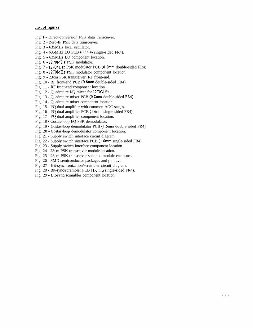
2. Direct-conversion PSK data transceiver
Similarly to a SSB transceiver, a PSK transceiver can also be built as a direct-conversion radio as shown onfig. 1. The Costas-loop demodulator can be extended to include most of the amplification in the receivingchain. Since such a receiver does not require narrow bandpass filters, the construction and alignment canbe much simplified. In addition, some receiver stages can also be used in the transmitter (like the localoscillator chain) to further simplify the overall transceiver.
A direct-conversion PSK receiver also has some problems. Limiting is generally not harmful in the signalamplifier, however it increases the noise in the error amplifier chain. In practice the loop bandwidth has tobe decreased, if no AGC is used and both amplifiers operate in the limiting regime. It is also very difficult
176
to have both amplifiers DC coupled as required by the theory. If AC coupled amplifiers are used,randomization (scrambling) has to be applied to the data stream and some additional noise is generated.However, in a well-designed, direct-conversion PSK receiver the signal-to-noise ratio degradation due toAC coupling can be kept sufficiently small.
Building a real-world, direct-conversion PSK receiver one should also consider other unwanted effects. Forexample, the Costas-loop demodulator includes very high-gain stages. Unwanted effects like AMmodulation on the VCO or FM-to-AM conversion in the multiplier stages can lead to unwanted feedbackloops. However, the most critical component seems to be the VCO.
In a practical microwave PSK transceiver the VCO is built as a VCXO followed by a multiplier chain.Although the static frequency-pulling range of fundamental-resonance and third-overtone crystals issufficient for this application, their dynamic response is totally unpredictable above 1kHz. The latter maybe enough for full-duplex, continuous-carrier microwave links, but it is insufIicient for CSMA packet-radio, where a very fast signal acquisition is required.
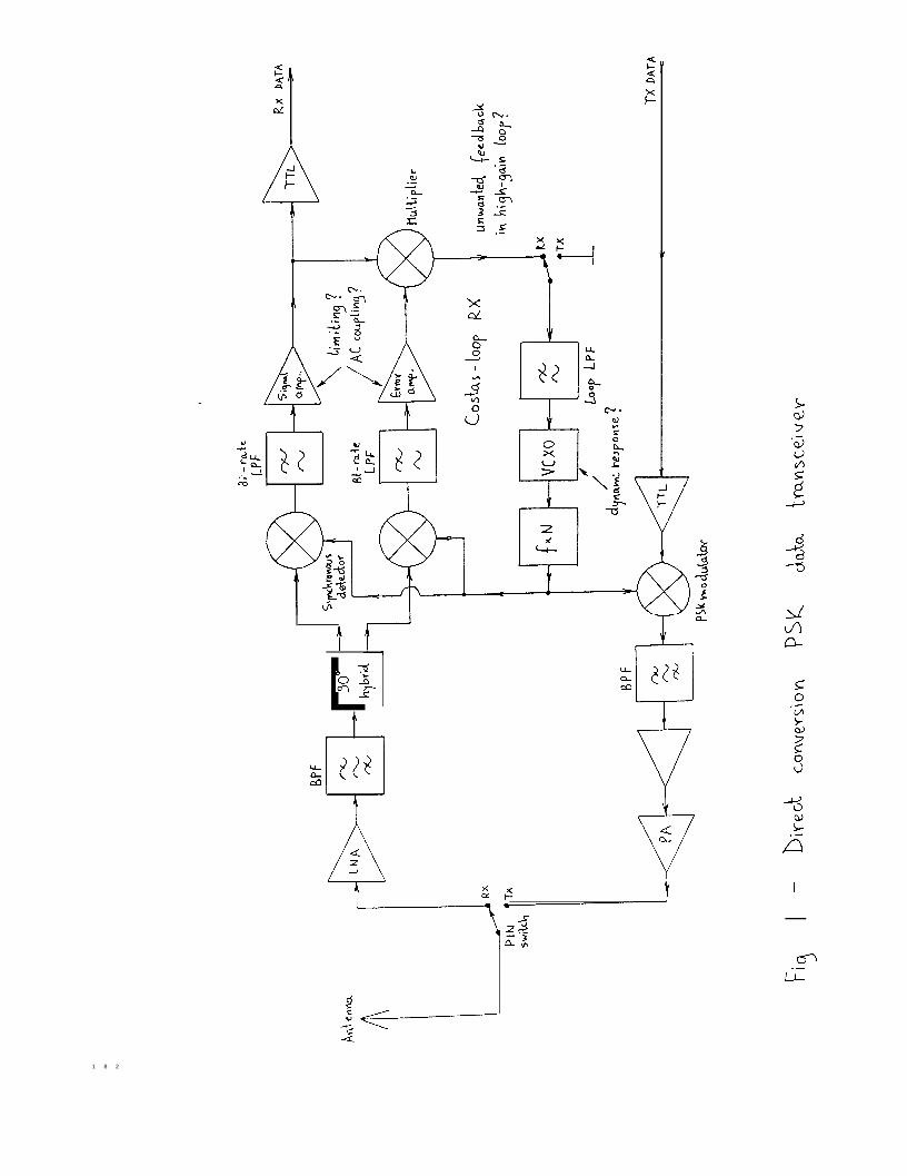
3. Zero-IF PSK data transceiver
Most of the problems of a direct-conversion PSK receiver can be overcome in a so called “zero-IF” PSKreceiver, as shown on fig.2. Incidentally, a zero-IF PSK transceiver requires very similar hardware to adirect-conversion PSK transceiver. The main difference is in the local oscillator. A zero-IF PSK receiverhas a fixed-frequency, free-running local oscillator, while the demodulation is only performed after themain receiver gain stages.
A zero-IF PSK receiver includes a quadrature mixer that provides two output signals I’ and Q’ with thesame bandwidth as in a direct-conversion RX. The signals I’ and Q’ contain all of the information of theinput RF signal, but they do not represent the demodulated signal yet. Since the zero-IF RX contains a free-running LO, its phase is certainly not matched to the transmitter. Further, if there is a difference betweenthe frequencies of the transmitter and of the receiver, the phasor represented by the I’ and Q’ signals willrotate at a rate corresponding to the difference of the two frequencies.
To demodulate the information, the I’ and Q’ signals have to be fed to a phase shifter to counter-rotate thephasor. The phase shifter is kept synchronized to the correct phase and rate by a Costas-loop feedback.Since the whole Costas-loop demodulator operates at high signal levels and at relatively low frequencies, itcan be built with inexpensive 74HCxxx logic circuits that require no tuning at all!
A zero-IF PSK receiver requires linear amplification of the I’ and Q’ signals. Limiting of the I’ and Q’signals is very harmful to the overall signal-to-noise ratio. If the zero-IF amplifiers are AC coupled, datarandomization (scrambling) is required. On the other hand, a zero-IF PSK transceiver does not include anycritical stages or unstable feedback loops and is therefore easily reproducible.
Searching for a simple PSK transceiver design I attempted to build both a direct-conversion and a zero-IFPSK transceiver for 23cm. The 23cm band offers sufficient bandwidth for 1.2Mbit/s operation. Further, thewhole transceiver can be built on conventional, inexpensive glassfiber-epoxy laminate FR4. Finally, thepropagation losses without optical visibility are smaller in the 23cm band than at higher microwavefrequencies.
A direct-conversion PSK transceiver for 2just one LM3 11 voltage comparator each,
3cm resulted veryoperating as a lim
simple. The signal and error amplifiers usediting amplifier. The only limitation of this
transceiver was the VCXO. Due to the undefined dynamic response of the VCXO, the capturing range ofthe Costas-loop RX was only about +/-SkHz. Further, even this figure was hardly reproducible, since eventwo crystals from the same manufacturing batch had a quite different dynamic response in the VCXO.
177
A zero-IF 23cm PSK transceiver resulted slightly more complex, due to the linear IF amplification withAGC and the additional Costas-loop demodulator. On the other hand, the zero-IF 23cm PSK RTX resultedfully reproducible, since there are no critical parts or unstable circuits built in. Since the additionalcomplexity of the zero-IF RTX is in the IF part, using only cheap components and no tuning points, it doesnot add much to the overall complexity of the transceiver.
4. Design of the zero-IF 23cm PSK transceiver
In this article I am therefore going to describe the abovementioned successful design of a zero-IF PStransceiver. The transceiver is built on seven printed-circuit boards, four of which (the RF part) areinstalled in metal shielded enclosures. The RF part is built mainly as microstrip circuits on 0.8mm thglassfiber-epoxy laminate FR4.
K data
ick
Subharmonic mixers are used both in the transmitter modulator and in the receiver quadrature mixer.Subharmonic mixers with two antiparallel diodes are simple to build. Since the L,O signal is at half of theRF frequency, RF signals are easier to decouple and less shielding is required. Finally, it is very easy tobuild two identical subharmonic mixers for the receiver quadrature mixer.
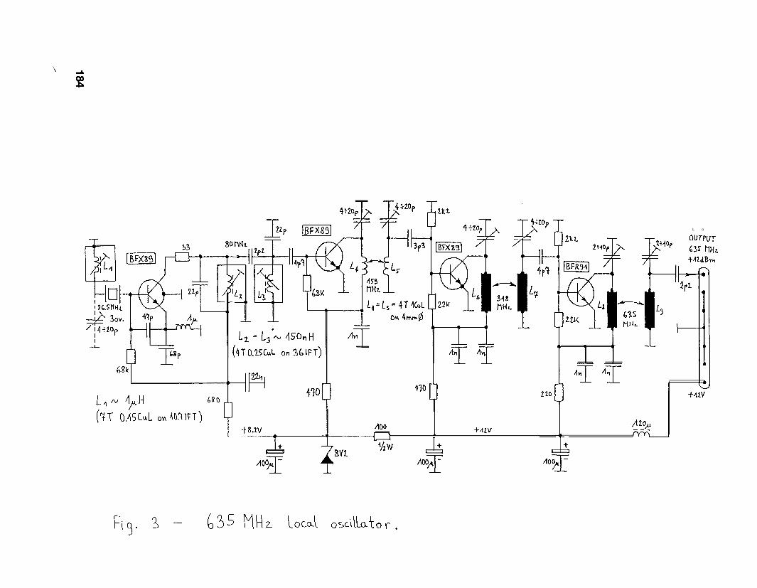
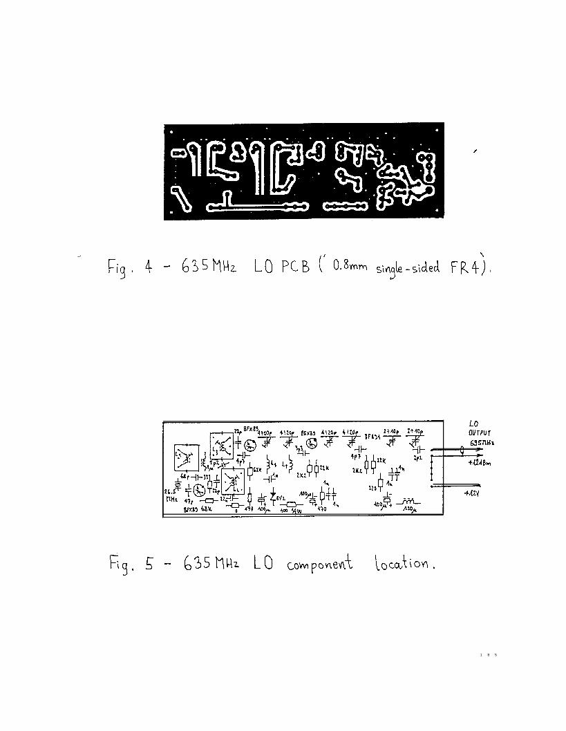
The whole transceiver therefore requires a single local oscillator operating at half of the RF frequency or atabout 635MHz for operation in the 23cm amateur band. The local oscillator including a crystal oscillatorand multiplier stages is shown on fig.3. The LO module is built on a single-sided PCB, as shown on fig.4and fig.5.
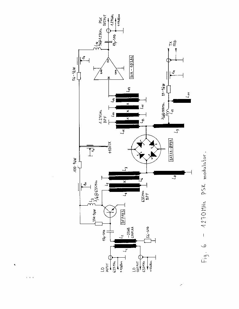
To speed-up the TX/RX switching, the receiving mixers are powered on and are receiving the LO signal allof the time. On the other hand, the LO signal feeding the modulator has to be turned off to avoid anyinterference during reception. Therefore the LO signal is fed to the receiving mixers through a directionalcoupler located in the 1270MHz PSK modulator module as shown on fig.6.
Only a small fraction of the LO power (-20dB) is fed to a separation amplifier stage (BFP183). The635MHz BPF ensures a good residual carrier suppression (>30dB) in the PSK modulator. The 1.27GHzBPF is used to suppress the 635MHz LO signal and its.unwanted harmonics. Finally, a two-stage MMICamplifier (INA- 10386) is used to boost the signal level to +I4dBm.
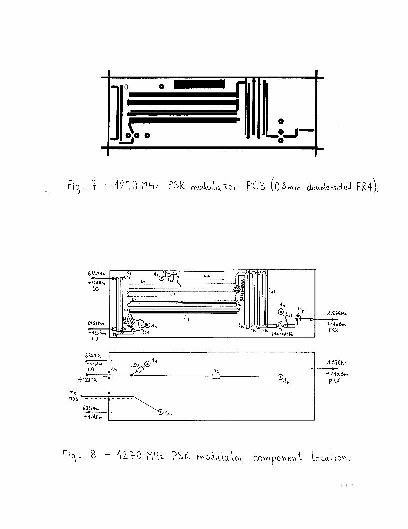
The 1270MHz PSK modulator is a microstrip circuit built on a double-sided PCB as shown on fig.7 andfig.8. The bottom side of the PCB is not etched to serve as a groundplane for the microstrip circuit. The RFsignal losses in the FR4 laminate are rather high at 1.27GHz. For example, the 1.27GHz BPF has apassband insertion loss of about 5dB. On the other hand, all of the microstrip bandpass filters are designedfor a bandwidth of more than 10% of the center frequency and therefore require no tuning considering thelaminate and etching tolerances.
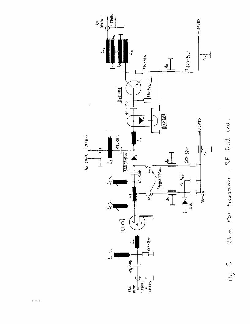
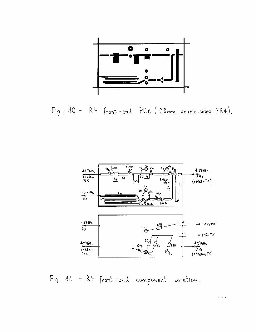
The RF front-end of the 23cm PSK transceiver, shown on fig.9, includes a TX power amplifier with aCLYS power GaAsFET to boost the TX output power to about 1 W (+30dBm), a PIN diode antenna switch(BAR63-03 W and BAR80) and a receiving RF amplifier with a BFP18 1. The latter has about 15dB gain,but the following 1.27GHz BPF has about 3dB passband loss. The RF front-end is also built as a microstripcircuit on a double-sided PCB as shown on fig. 10 and fig. 11.
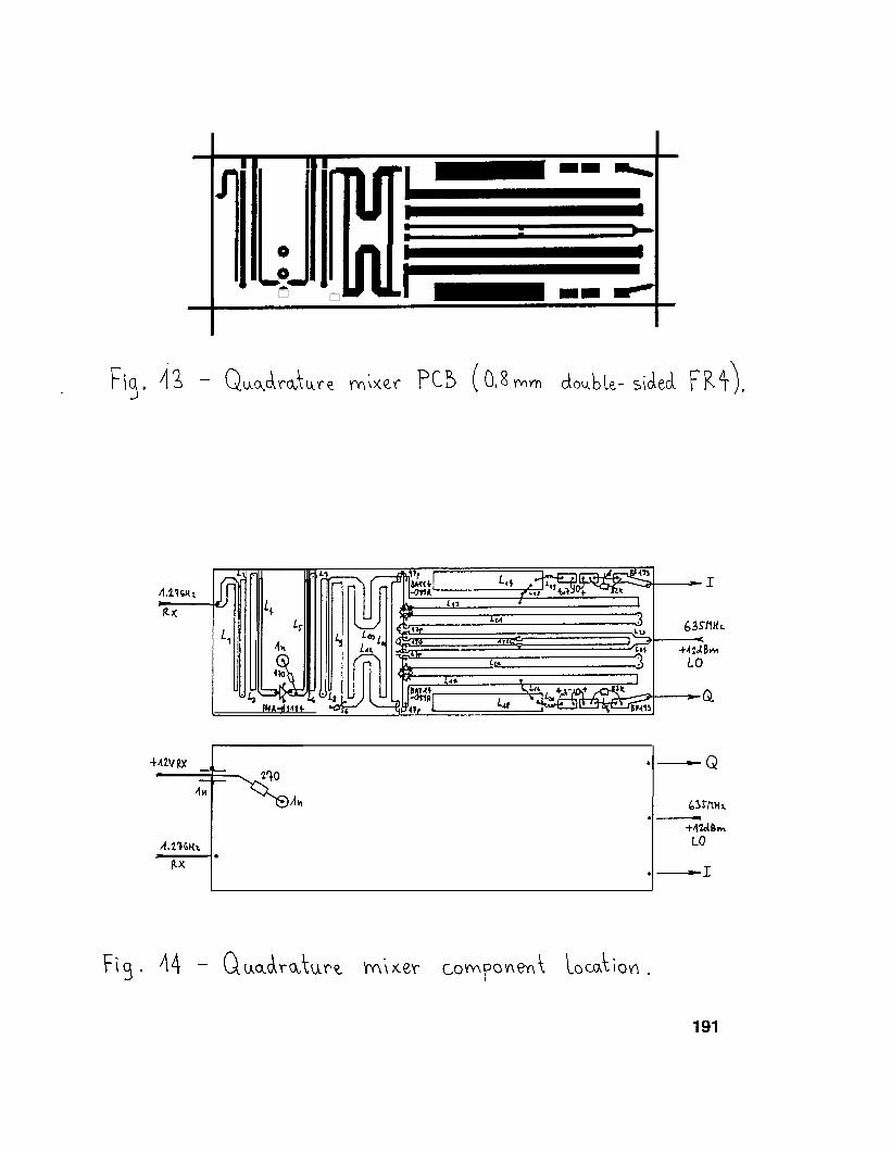
The quadrature I/Q mixer for 1270MHz, shown on fig. 12, includes an additional gain stage at 1.27GHz(26dB MMIC INA- I84), two bandpass filters at 1.27GHz (3dB insertion loss each), a quadrature hybridfor the RF signal at 1.27GHz, an in-phase power splitter for the LO signal at 635MHz, two identicalsubharmonic mixers (two BAT1 4-099R schottky quads) and two identical IF preamplifiers (two BF 199).
Since the termination impedances of the subharmonic mixers depend on the LO signal power, thedifference ports of both the quadrature (RF) and in-phase (LO) power splitters have to be terminated toensure the correct phase and amplitude relationships. Considering the manufacturing tolerances of the
178
microstrip PCB shown on fig. 13 and fig. 14, the amplitushift is within +l-5degrees from the nominal 90degrees.
.de matching is usual ly within 5% and the phase
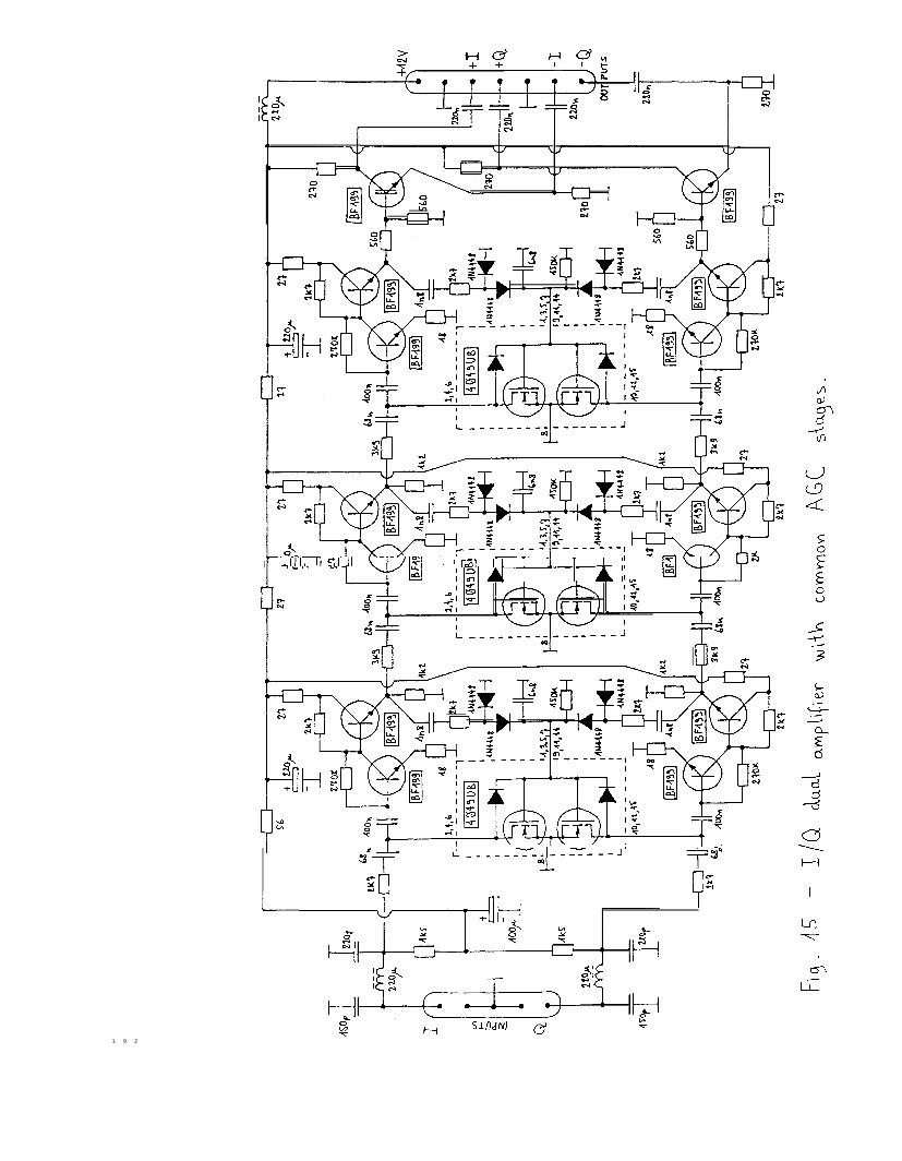
A zero-IF receiver requires a dual IF amplifier with two identical amplification channels, but a single,common AGC. Since DC-coupled amplifiers can not be built, the lower frequency limit of AC-coupledstages has to be set sufficiently low. At a data rate of 1.2Mbit/s, a convenient choice is a lower frequencylimit of 1 kHz. The latter allows all of the time constants in the range of lms (TX/RX switching time!) andcauses a distortion of about 4% of the amplitude of the IF signal.
Of course the AGC time constant should also be in the same range around lms. Such a fast AGC can onlybe applied to low gain stages to avoid unwanted feedback. A simple technical solution is to use more thanone AGC in the IF amplifier chain. The I/Q dual amplifier shown on fig. 15 has three identical dualamplifier stages and each of these dual stages has its own AGC circuit using MOS transistors (4049UB) asvariable resistors.
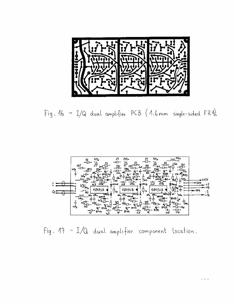
The I/Q dual amplifier module also includes two identical lowpass filters on the input (that define thereceiver bandwidth) and two phase inversion stages on the output to obtain a four-phase output signal (+I,+Q, -I and -Q) to drive the following phase shifter. The I/Q dual amplifier is built on a single-sided PCB asshown on fig. 16 and fig. 17.
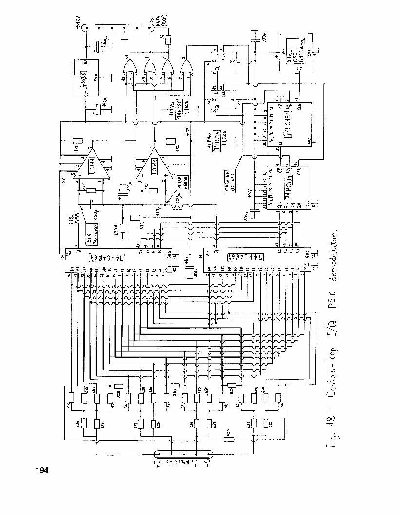
The Costas-loop I/Q PSK demodulator is built entirely using cheap 74HCxxx logic as shown on fig. 18.The four-phase input signal (+I, +Q, -I and -Q) feeds a resistor network that generates a multiphase systemwith a large number (16) of phases. Two 74HC4067 analog switches are then used to select the desiredsignal phase. The inputs of the two analog selectors are offset by 4 to provide the required 90-degree phaseshift between the signal and error outputs.
Both the signal and error are first fed through two lowpass filters (to suppress the 74HC4067 switchingtransients) and finally to two LM3 11 voltage comparators to obtain TLL-level signals. The signal and errorare then multiplied in an EXOR gate and feed a digital VCO. The digital VCO includes a 6.144MHz clockoscillator and two 74HC191 up/down counters.
The up/down control is used as the VCO control input. If the latter is at a logical ZERO, the up/downcounter rotates the two 74HC4067 switches FORWARD with a frequency of 24kHz. If the input is at alogical ONE, the up/down counter rotates the two 74HC4067 switches BACKWARD with a frequency of24kHz. Finally, if the control input toggles, the result depends on the ON/OFF ratio of the control signal.At 50% duty the 74HC4067 switches stay in the same position.
The overall circuit therefore operates as a first-order, Costas phase-locked loop that is able to correctcarrier-frequency errors between -24kHz and +24kHz. The loop gain is defined by the dividing ratio of the74HC191 up/down counters and the clock frequency. If a wider capturing range is desired, the clockfrequency can be increased up to 20MHz, but the resulting higher loop gain also increases the phase noise!
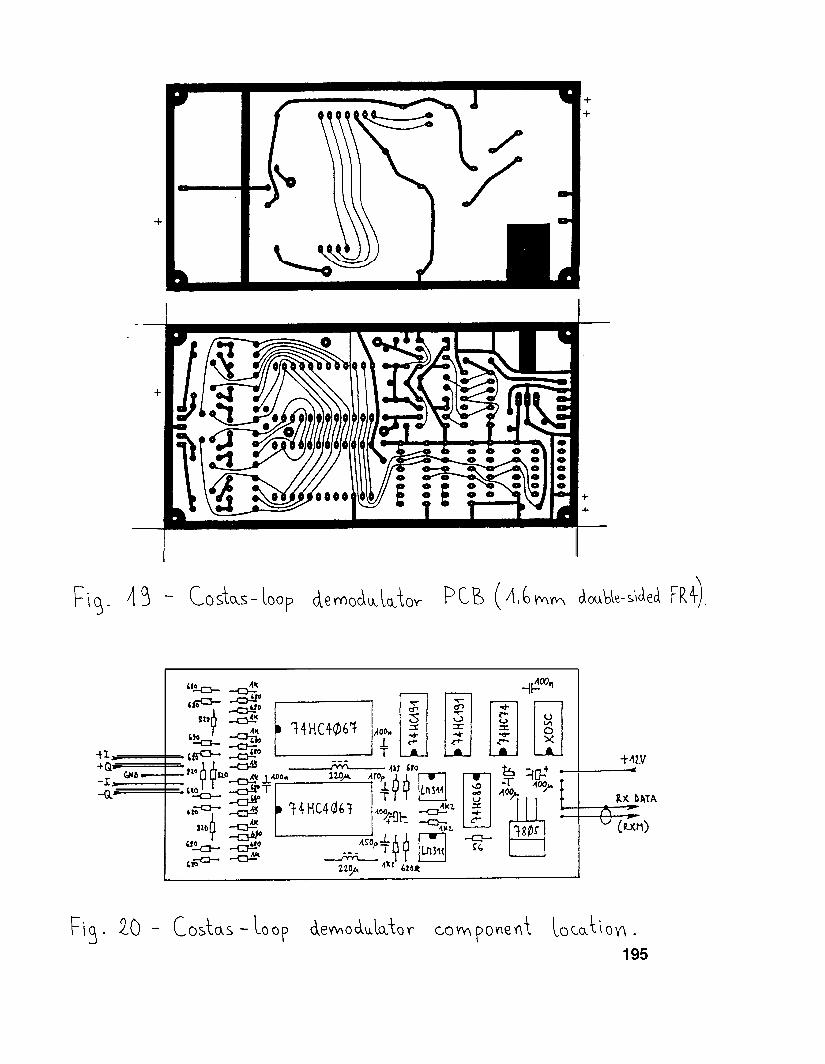
The Costas-loop demodulator is built on a double-sided PCB as shown on fig. 19 and fig.20. The circuitincludes its own +5V regulator and an output stage capable of feeding a 75-ohm cable with thedemodulated RX data.
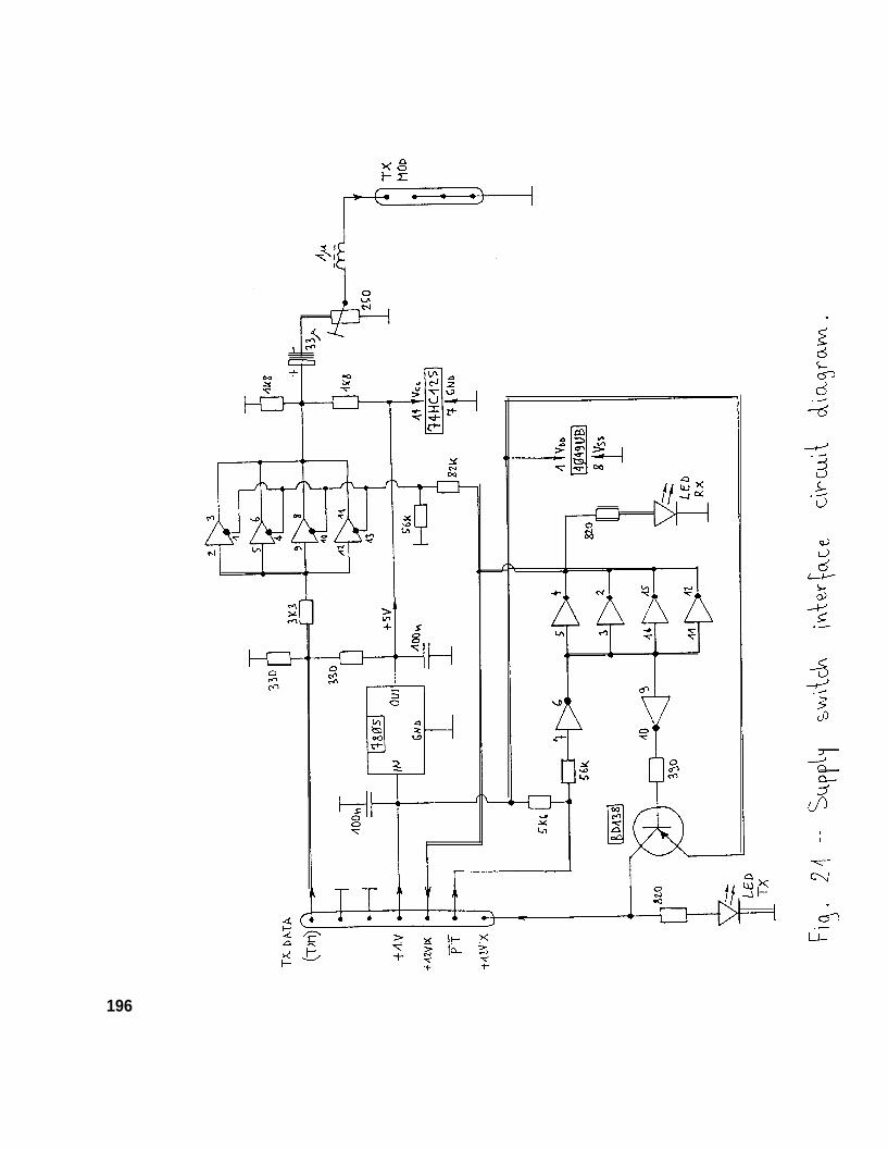
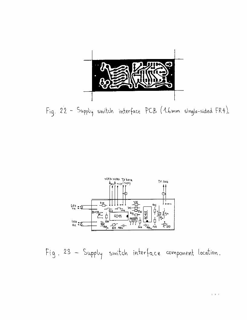
The overall PSK transceiver requires a few additional interface circuits (shown on fig.21) including asupply voltage switch and a modulator driver. The modulator driver includes a lowpass filter to decreasethe high-order sidelobes of the modulation spectrum. The supply switch interface is built on a single-sidedPCB as shown on fig.22 and fig.23.
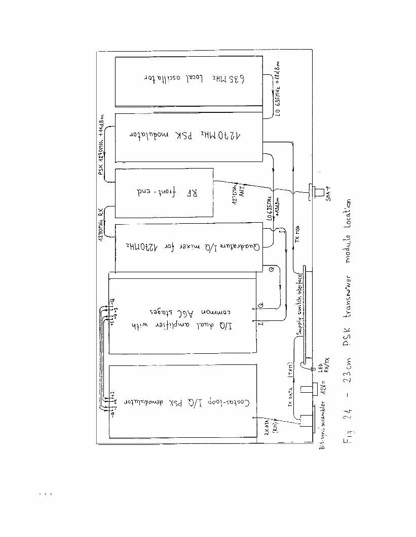
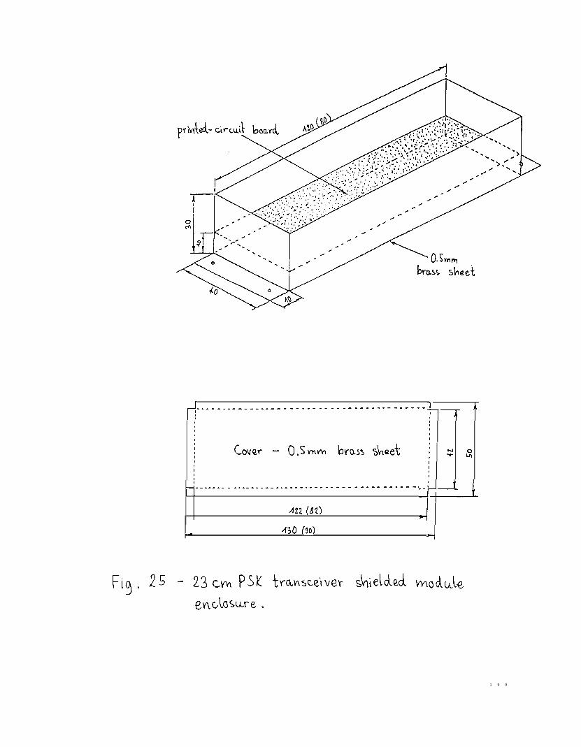
The overall PSK transceiver is enclosed in an aluminum box with the dimensions of 320mm (width) X175mm (depth) X 32mm (height). The location of the single modules is shown on fig.24. The four RFmodules are additionally shielded in small boxes made of 0.5mm thick brass sheet as shown on fig.25. The
1 7 9
groundplane of the PCBs is soldered along all four sides to the brass frame to ensure a good electricalcontact.
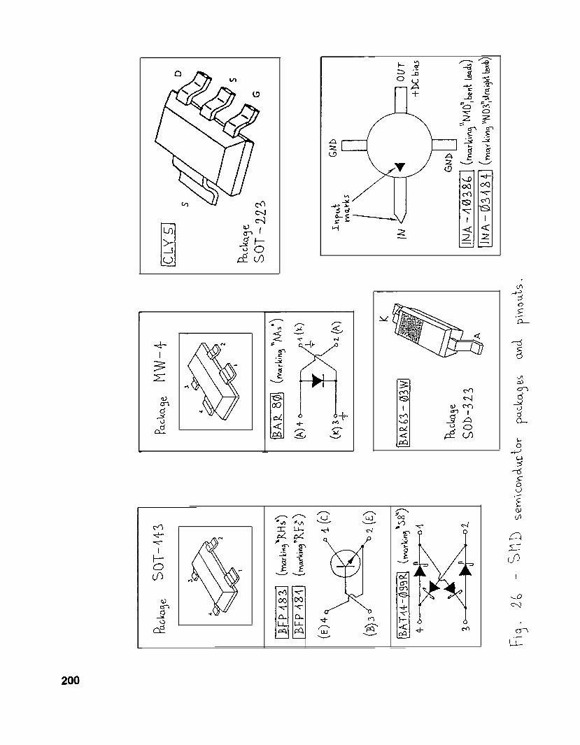
Special care should be devoted to the assembly of the microstrip circuits. The microstrip resonators aregrounded at the marked positions using 0.6mm thick CuAg wire. The SMD components (shown on fig.26)are grounded through 2Smm, 3.2mm or 5mm diameter holes at the marked positions. The holes are firstcovered with a piece of thin copper sheet on the groundplane side, then they are filled with solder andfinally the SMD part is soldered in place.
The assembled PSK transceiver requires little tuning. The only module that needs to be tuned in any case isthe local oscillator module. Since most of the stages are just frequency doublers, it is very difficult to tunethis module to the wrong harmonic. The TX power amplifier may need some tuning to get the maximumoutput power. As printed on the circuit board, Ll in the RF power amplifier should not require any tuningif the interconnecting 50-ohm teflon cable from the modulator is exactly 12cm long. Tuning L3 and L6 theoutput power can only be increased by less than 1OOm W. All of the other microstrip resonators should notbe tuned. Finally, the 2500hm trimmer in the supply switch interface is adjusted for the maximum TXoutput power (usually 2/3 of the full scale),
5. Interfacing the 1,2Mbit/s PSK transceiver
Amateur packet-radio interfaces for data-rates above lOOkbit/s are not very popular. One of the mostpopular serial interfaces, the Zilog 28530 SCC, only includes a DPLL for RX clock recovery that canoperate up to about 250kbit/s. Other integrated circuits, like the old Z8OSI0, the MC68302 used in theTNC3 or the new MC68360 do not include any clock recovery circuits at all. In addition to the RX clockrecovery, data scrambling/descrambling and sometimes even NRZ/NRZI differential encoding/decodinghave to be provided by external circuits.
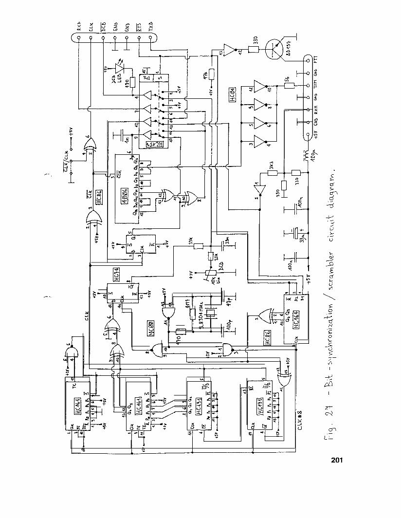
The circuit shown on fig.27 was specially designed to interface the described PSK transceiver to a 28530SCC, although it will probably work with other serial HDLC controllers as well. The circuit includes aninterpolation DPLL that only requires an s-times higher clock frequency (9.8304MHz), although providesthe resolution of a /256 conventional DPLL with a 3 15MHz clock.
The scrambler/descrambler uses a shift register with a linear feedback with EXOR gates. The scramblingpolynomial is the same as the one used in K9NG/G3RUH modems: 1+X** 12+X** 17. Due to theredundancy in the AX.25 data stream (zero insertion and deletion), a simple polynomial scrambler iscompletely sufficient to overcome the AC coupling limitation of the described PSK transceivers.
The interface circuit also includes 75ohm line drivers and receivers, if the PSK transceiver is installed atsome distance from the interface. However, connections have to be kept short on the side towards thecomputer serial port. The described interface only provides one clock signal, since it is intended forsimplex operation with the described PSK transceiver. Of course the DPLL is disabled duringtransmission, so that the circuit supplies a stable clock to the transmitter. The polarity of the clock signalcan be selected with a jumper. When using the 28530 RTxC or TRxC clock inputs, this jumper should beconnected to ground.
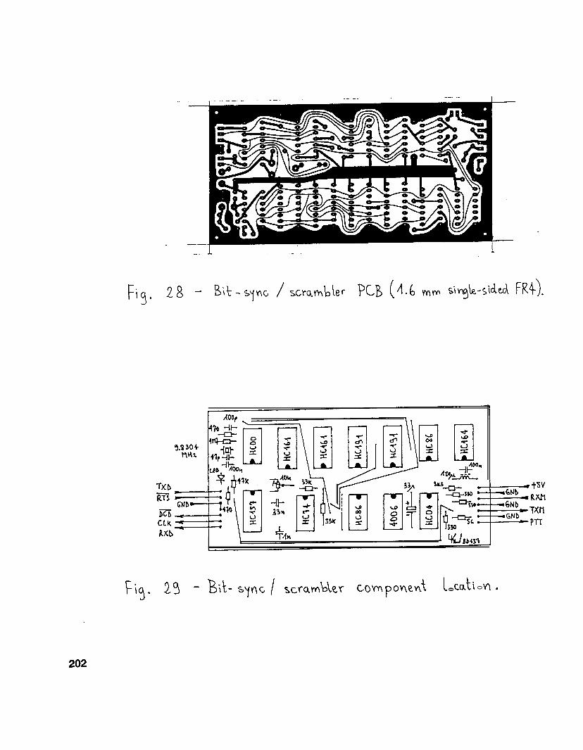
The bit-synchronization/scrambler circuit is built on a single-sided PCB as shown on fig.28 and fig.29. Itonly requires one adjustment, the DCD treshold, and the latter can only be performed when noise is presenton the RXM input.
1 8 0
List of figures:
Fig. 1 - Direct-conversion PSK data transceiver.Fig. 2 - Zero-IF PSK data transceiver.Fig. 3 - 635MHz local oscillator.Fig. 4 - 635MHz LO PCB (0.8mm single-sided FR4).Fig. 5 - 635MHz LO component location.Fig. 6 - 1270MHz PSK modulator.Fig. 7 - 1270MHz PSK modulator PCB (0.8mm double-sided FR4).Fig. 8 - 1270MHz PSK modulator component location.Fig. 9 - 23cm PSK transceiver, RF front-end.Fig. 10 - RF front-end PCB (0.8mm double-sided FR4).Fig. 11 - RF front-end component location.Fig. 12 - Quadrature I/Q mixer for 1270MHz.Fig. 13 - Quadrature mixer PCB (0.8mm double-sided FR4).Fig. 14 - Quadrature mixer component location.Fig. 15 - I/Q dual amplifier with common AGC stages.Fig. 16 - I/Q dual amplifier PCB (1.6mm single-sided FR4).Fig. 17 - I/Q dual amplifier component location.Fig. 18 - Costas-loop I/Q PSK demodulator.Fig. 19 - Costas-loop demodulator PCB (1.6mm double-sided FR4).Fig. 20 - Costas-loop demodulator component location.Fig. 21 - Supply switch interface circuit diagram.Fig. 22 - Supply switch interface PCB (1.6mm single-sided FR4).Fig. 23 - Supply switch interface component location.Fig. 24 - 23cm PSK transceiver module location.Fig. 25 - 23cm PSK transceiver shielded module enclosure.Fig. 26 - SMD semiconductor packages and pinouts.Fig. 27 - Bit-synchronization/scrambler circuit diagram.Fig. 28 - Bit-sync/scrambler PCB (1.6mm single-sided FR4).Fig. 29 - Bit-sync/scrambler component location.
1 8 1
1 , 1
IJLAA_t 3LOg -;i-z--
I
1 8 2
_-
1 8 3
L2 = &J 45&H
(4T 0.2SCd On 36iFT)
Fig 3 -
+42v1 A -?
+ +I 1 ‘/zw t 1 t 1
no0 -FL--
/loo --JI
L o
OWTJr63s Nljr+AZdBv,
-_. I \
Fig. 4 - 63Wk LO PcB ( O.grn, si$e-&d FR4) .
1 8 5
3
s
I I
1 8 6
Ill 0 O -
1 8 7
3ssT
1 8 8
I
t
1 8 9

/1.23GHt 4,21wrBPF BPF
/z1 --r f-
900 t-N2
.21 GHz
L 22J LA6
YII--OI)TPOT
a l 1
1111
I -0
0
0 0uu
-I JIII J 9-J ‘ra -I-
I I t:
3 L. --__------------1
J
J
-5dls; 6zc(
1 9 2
- + \ i-r l I - - -
1 9 3
+
++
c
dt-
196
llb438
1 9 7
.
c
I I at
t
4L
xsa!
s0. -
.-2
1 9 8
---I-------------------------------------F7-T
IIIIIIIIIIIIII
zI II I--------a w--- ____-__------------------------- t
A22 (80-Y
H- 430 (90,A
1 9 9
N 0 h)
,
c 0 F C*
0 5