Embed Size (px)
Citation preview
PSC Form - FR-0320 (02/20/03) Page 1 of 7
2380 Bering Dr. • San Jose, CA 95131 • USA
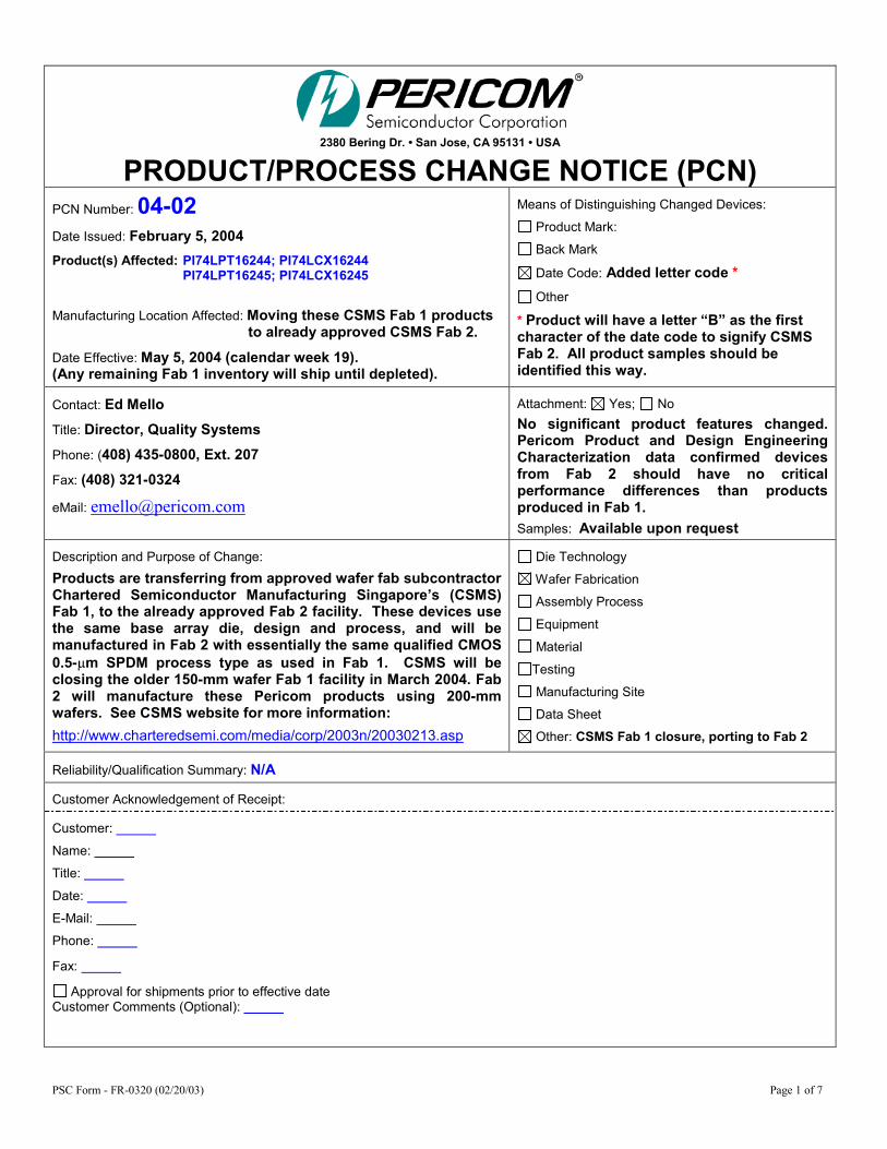
PRODUCT/PROCESS CHANGE NOTICE (PCN)PCN Number: 04-02Date Issued: February 5, 2004Product(s) Affected: PI74LPT16244; PI74LCX16244
PI74LPT16245; PI74LCX16245
Manufacturing Location Affected: Moving these CSMS Fab 1 productsto already approved CSMS Fab 2.
Date Effective: May 5, 2004 (calendar week 19). (Any remaining Fab 1 inventory will ship until depleted).
Means of Distinguishing Changed Devices:
Product Mark:
Back Mark
Date Code: Added letter code * Other
* Product will have a letter “B” as the firstcharacter of the date code to signify CSMSFab 2. All product samples should beidentified this way.
Contact: Ed MelloTitle: Director, Quality SystemsPhone: (408) 435-0800, Ext. 207Fax: (408) 321-0324
eMail: [email protected]
Attachment: Yes; No No significant product features changed.Pericom Product and Design EngineeringCharacterization data confirmed devicesfrom Fab 2 should have no criticalperformance differences than productsproduced in Fab 1.Samples: Available upon request
Description and Purpose of Change: Products are transferring from approved wafer fab subcontractorChartered Semiconductor Manufacturing Singapore’s (CSMS)Fab 1, to the already approved Fab 2 facility. These devices usethe same base array die, design and process, and will bemanufactured in Fab 2 with essentially the same qualified CMOS0.5-�m SPDM process type as used in Fab 1. CSMS will beclosing the older 150-mm wafer Fab 1 facility in March 2004. Fab2 will manufacture these Pericom products using 200-mmwafers. See CSMS website for more information:http://www.charteredsemi.com/media/corp/2003n/20030213.asp
Die Technology
Wafer Fabrication
Assembly Process
Equipment
Material
Testing
Manufacturing Site
Data Sheet
Other: CSMS Fab 1 closure, porting to Fab 2
Reliability/Qualification Summary: N/A
Customer Acknowledgement of Receipt:
Customer: Name: Title: Date: E-Mail: Phone:
Fax:
Approval for shipments prior to effective dateCustomer Comments (Optional):
PI74LCX16245 - 2 -
Confidential/For Customer Use Only
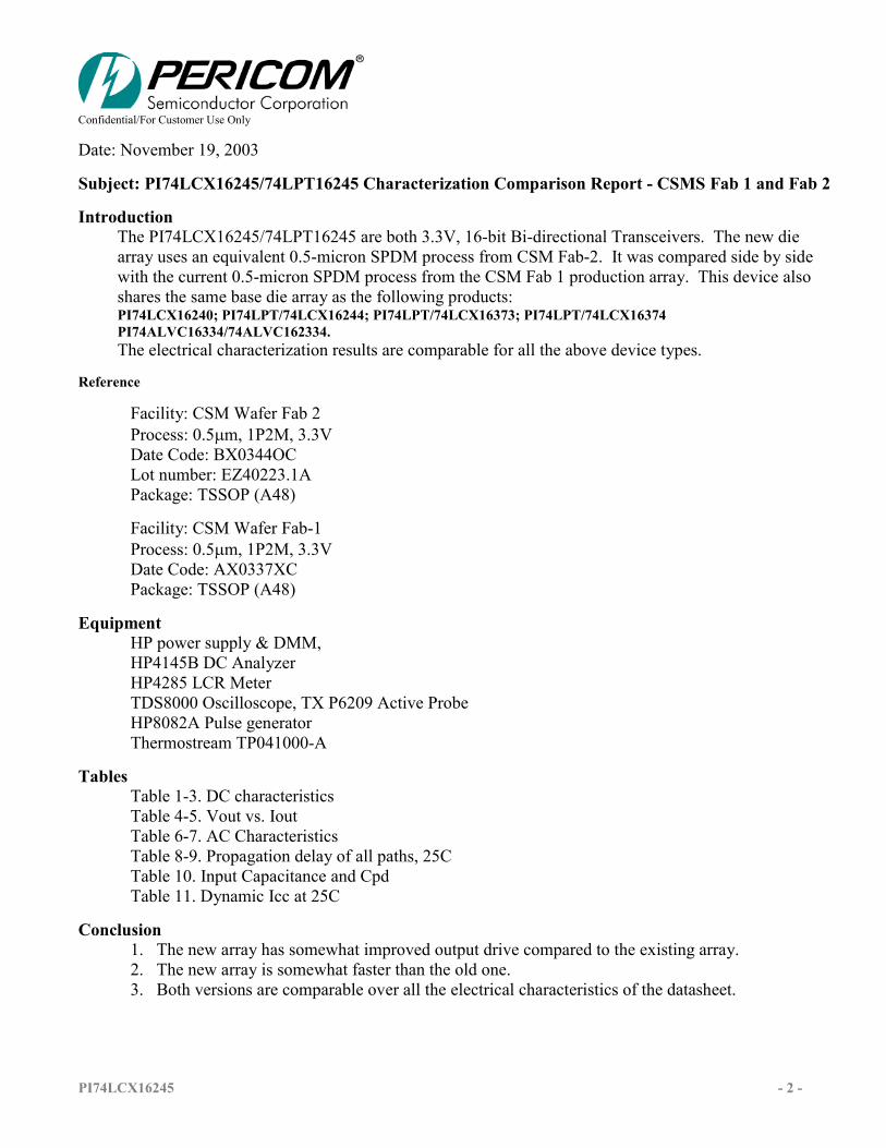
Date: November 19, 2003
Subject: PI74LCX16245/74LPT16245 Characterization Comparison Report - CSMS Fab 1 and Fab 2
IntroductionThe PI74LCX16245/74LPT16245 are both 3.3V, 16-bit Bi-directional Transceivers. The new diearray uses an equivalent 0.5-micron SPDM process from CSM Fab-2. It was compared side by sidewith the current 0.5-micron SPDM process from the CSM Fab 1 production array. This device alsoshares the same base die array as the following products:PI74LCX16240; PI74LPT/74LCX16244; PI74LPT/74LCX16373; PI74LPT/74LCX16374PI74ALVC16334/74ALVC162334.The electrical characterization results are comparable for all the above device types.
Reference
Facility: CSM Wafer Fab 2 Process: 0.5�m, 1P2M, 3.3VDate Code: BX0344OCLot number: EZ40223.1APackage: TSSOP (A48)
Facility: CSM Wafer Fab-1Process: 0.5�m, 1P2M, 3.3VDate Code: AX0337XCPackage: TSSOP (A48)
EquipmentHP power supply & DMM, HP4145B DC AnalyzerHP4285 LCR MeterTDS8000 Oscilloscope, TX P6209 Active ProbeHP8082A Pulse generatorThermostream TP041000-A
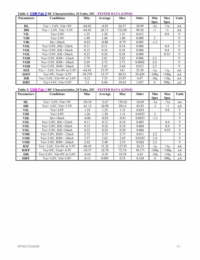
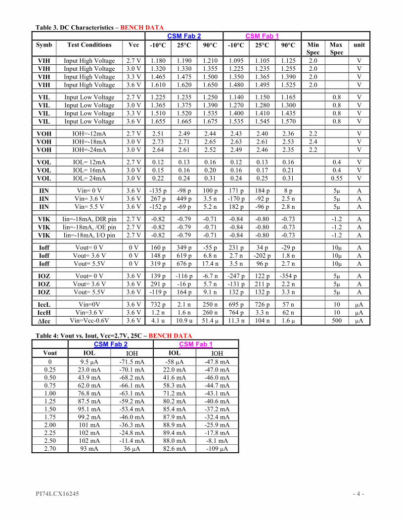
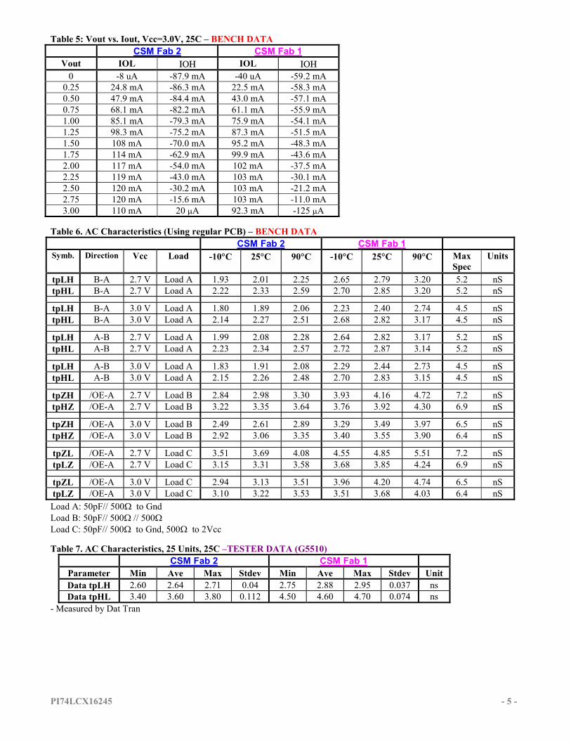
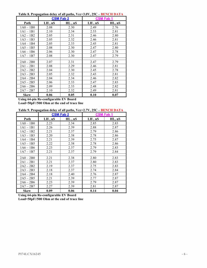
TablesTable 1-3. DC characteristicsTable 4-5. Vout vs. IoutTable 6-7. AC Characteristics Table 8-9. Propagation delay of all paths, 25CTable 10. Input Capacitance and CpdTable 11. Dynamic Icc at 25C
Conclusion1. The new array has somewhat improved output drive compared to the existing array.2. The new array is somewhat faster than the old one.3. Both versions are comparable over all the electrical characteristics of the datasheet.
PI74LCX16245 - 3 -
Table 1: CSM Fab 2 DC Characteristics, 25 Units, 25C –TESTER DATA (G5510)Parameters Conditions Min. Average Max Stdev Min
SpecMaxSpec
Units
IIL Vcc = 3.6V, Vin= 0V -64.45 -4.93 64.27 20.99 -1u +1u nAIIH Vcc = 3.6V, Vin= 5.5V -64.45 26.71 722.69 90.36 -1 +1 nAVIL Vcc=3.0V 1.25 1.30 1.31 0.012 0.8 VVIH Vcc=3.0V 1.40 1.40 1.40 0.000 2 VVIK Iin=-18mA -0.83 -0.80 -0.79 0.005 -1.2 VVOL Vcc=3.0V, IOL=12mA 0.11 0.11 0.14 0.004 0.4 VVOL Vcc=3.0V, IOL=16mA 0.15 0.16 0.18 0.006 0.4 VVOL Vcc=3.0V, IOL=24mA 0.23 0.24 0.28 0.009 0.55 VVOH Vcc=3.0V, IOH= -12mA 2.79 2.81 2.82 0.006 2.2 VVOH Vcc=3.0V, IOH= -18mA 2.69 2.72 2.73 0.0092 2.4 VVOH Vcc=3.0V, IOH= -24mA 2.58 2.62 2.64 0.012 2.2 VIOZ Vcc = 3.6V, Vo=0V or 5.5V -64.45 31.97 141 55.30 -1� +1� nA
IOFF Vcc=0V, Vout= 4.5V -38.379 15.37 80.23 29.429 -100� +100� nAISB Vcc=3.6V, Vin=0V or 3.6V -8.21 7.35 23.07 6.07 -10� +10� nA
ISBT Vcc=3.6V, Vin=3.0V 7.2 8.84 10.65 1.057 0 500� �A
Table 2: CSM Fab 1 DC Characteristics, 25 Units, 25C –TESTER DATA (G5510)Parameters Conditions Min. Average Max Stdev Min
SpecMaxSpec
Units
IIL Vcc= 3.6V, Vin= 0V -50.18 -2.67 | 95.62 24.69 -1u +1u nAIIH Vcc= 3.6V, Vin= 5.5V -61.13 24.98 581.6 83.83 -1 +1 nAVIL Vcc=3.0V 1.18 1.25 1.31 0.034 0.8 VVIH Vcc=3.0V 1.26 1.30 1.31 0.0187 2 VVIK Iin=-18mA -0.86 -0.82 -0.81 0.0033 -1.2 VVOL Vcc=3.0V, IOL=12mA 0.11 0.12 0.14 0.003 0.4 VVOL Vcc=3.0V, IOL=16mA 0.15 0.16 0.19 0.004 0.4 VVOL Vcc=3.0V, IOL=24mA 0.23 0.24 0.29 0.006 0.55 VVOH Vcc=3.0V, IOH= -12mA 2.72 2.75 2.77 0.011 2.2 VVOH Vcc=3.0V, IOH= -18mA 2.57 2.62 2.65 0.0182 2.4 VVOH Vcc=3.0V, IOH= -24mA 2.42 2.48 2.53 0.026 2.2 VIOZ Vcc= 3.6V, Vo=0V or 5.5V -46.45 31.22 127.91 56.23 -1� +1� nA
IOFF Vcc=0V, Vout= 4.5V -38.37 16.78 72.74 30.171 -100� +100� nAISB Vcc=3.6V, Vin=0V or 3.6V -6.64 4.10 18.38 6.63 -10� +10� nA
ISBT Vcc=3.6V, Vin=3.0V -0.13 0.085 0.33 0.168 0 500� �A
PI74LCX16245 - 4 -
Table 3. DC Characteristics – BENCH DATACSM Fab 2 CSM Fab 1
Symb Test Conditions Vcc -10�C 25�C 90�C -10�C 25�C 90�C MinSpec
Max Spec
unit
VIH Input High Voltage 2.7 V 1.180 1.190 1.210 1.095 1.105 1.125 2.0 VVIH Input High Voltage 3.0 V 1.320 1.330 1.355 1.225 1.235 1.255 2.0 VVIH Input High Voltage 3.3 V 1.465 1.475 1.500 1.350 1.365 1.390 2.0 VVIH Input High Voltage 3.6 V 1.610 1.620 1.650 1.480 1.495 1.525 2.0 V
VIL Input Low Voltage 2.7 V 1.225 1.235 1.250 1.140 1.150 1.165 0.8 VVIL Input Low Voltage 3.0 V 1.365 1.375 1.390 1.270 1.280 1.300 0.8 VVIL Input Low Voltage 3.3 V 1.510 1.520 1.535 1.400 1.410 1.435 0.8 VVIL Input Low Voltage 3.6 V 1.655 1.665 1.675 1.535 1.545 1.570 0.8 V
VOH IOH=-12mA 2.7 V 2.51 2.49 2.44 2.43 2.40 2.36 2.2 VVOH IOH=-18mA 3.0 V 2.73 2.71 2.65 2.63 2.61 2.53 2.4 VVOH IOH=-24mA 3.0 V 2.64 2.61 2.52 2.49 2.46 2.35 2.2 V
VOL IOL= 12mA 2.7 V 0.12 0.13 0.16 0.12 0.13 0.16 0.4 VVOL IOL= 16mA 3.0 V 0.15 0.16 0.20 0.16 0.17 0.21 0.4 VVOL IOL= 24mA 3.0 V 0.22 0.24 0.31 0.24 0.25 0.31 0.55 V
IIN Vin= 0 V 3.6 V -135 p -98 p 100 p 171 p 184 p 8 p 5� AIIN Vin= 3.6 V 3.6 V 267 p 449 p 3.5 n -170 p -92 p 2.5 n 5� AIIN Vin= 5.5 V 3.6 V -152 p -69 p 5.2 n 182 p -96 p 2.8 n 5� A
VIK Iin=-18mA, DIR pin 2.7 V -0.82 -0.79 -0.71 -0.84 -0.80 -0.73 -1.2 AVIK Iin=-18mA, /OE pin 2.7 V -0.82 -0.79 -0.71 -0.84 -0.80 -0.73 -1.2 AVIK Iin=-18mA, I/O pin 2.7 V -0.82 -0.79 -0.71 -0.84 -0.80 -0.73 -1.2 A
Ioff Vout= 0 V 0 V 160 p 349 p -55 p 231 p 34 p -29 p 10� AIoff Vout= 3.6 V 0 V 148 p 619 p 6.8 n 2.7 n -202 p 1.8 n 10� AIoff Vout= 5.5V 0 V 319 p 676 p 17.4 n 3.5 n 96 p 2.7 n 10� A
IOZ Vout= 0 V 3.6 V 139 p -116 p -6.7 n -247 p 122 p -354 p 5� AIOZ Vout= 3.6 V 3.6 V 291 p -16 p 5.7 n -131 p 211 p 2.2 n 5� AIOZ Vout= 5.5V 3.6 V -119 p 164 p 9.1 n 132 p 132 p 3.3 n 5� A
IccL Vin=0V 3.6 V 732 p 2.1 n 250 n 695 p 726 p 57 n 10 �AIccH Vin=3.6 V 3.6 V 1.2 n 1.6 n 260 n 764 p 3.3 n 62 n 10 �A�Icc Vin=Vcc-0.6V 3.6 V 4.1 u 10.9 u 51.4 � 11.3 n 104 n 1.6 � 500 �A
Table 4: Vout vs. Iout, Vcc=2.7V, 25C – BENCH DATACSM Fab 2 CSM Fab 1
Vout IOL ��� IOL ���
0 9.5 �A -71.5 mA -58 �A -47.8 mA0.25 23.0 mA -70.1 mA 22.0 mA -47.0 mA0.50 43.9 mA -68.2 mA 41.6 mA -46.0 mA0.75 62.0 mA -66.1 mA 58.3 mA -44.7 mA1.00 76.8 mA -63.1 mA 71.2 mA -43.1 mA1.25 87.5 mA -59.2 mA 80.2 mA -40.6 mA1.50 95.1 mA -53.4 mA 85.4 mA -37.2 mA1.75 99.2 mA -46.0 mA 87.9 mA -32.4 mA2.00 101 mA -36.3 mA 88.9 mA -25.9 mA2.25 102 mA -24.8 mA 89.4 mA -17.8 mA2.50 102 mA -11.4 mA 88.0 mA -8.1 mA2.70 93 mA 36 �A 82.6 mA -109 �A
PI74LCX16245 - 5 -
Table 5: Vout vs. Iout, Vcc=3.0V, 25C – BENCH DATACSM Fab 2 CSM Fab 1
Vout IOL ��� IOL ���
0 -8 uA -87.9 mA -40 uA -59.2 mA0.25 24.8 mA -86.3 mA 22.5 mA -58.3 mA0.50 47.9 mA -84.4 mA 43.0 mA -57.1 mA0.75 68.1 mA -82.2 mA 61.1 mA -55.9 mA1.00 85.1 mA -79.3 mA 75.9 mA -54.1 mA1.25 98.3 mA -75.2 mA 87.3 mA -51.5 mA1.50 108 mA -70.0 mA 95.2 mA -48.3 mA1.75 114 mA -62.9 mA 99.9 mA -43.6 mA2.00 117 mA -54.0 mA 102 mA -37.5 mA2.25 119 mA -43.0 mA 103 mA -30.1 mA2.50 120 mA -30.2 mA 103 mA -21.2 mA2.75 120 mA -15.6 mA 103 mA -11.0 mA3.00 110 mA 20 �A 92.3 mA -125 �A
Table 6. AC Characteristics (Using regular PCB) – BENCH DATACSM Fab 2 CSM Fab 1
Symb. Direction Vcc Load -10�C 25�C 90�C -10�C 25�C 90�C MaxSpec
Units
tpLH B-A 2.7 V Load A 1.93 2.01 2.25 2.65 2.79 3.20 5.2 nStpHL B-A 2.7 V Load A 2.22 2.33 2.59 2.70 2.85 3.20 5.2 nS
tpLH B-A 3.0 V Load A 1.80 1.89 2.06 2.23 2.40 2.74 4.5 nStpHL B-A 3.0 V Load A 2.14 2.27 2.51 2.68 2.82 3.17 4.5 nS
tpLH A-B 2.7 V Load A 1.99 2.08 2.28 2.64 2.82 3.17 5.2 nStpHL A-B 2.7 V Load A 2.23 2.34 2.57 2.72 2.87 3.14 5.2 nS
tpLH A-B 3.0 V Load A 1.83 1.91 2.08 2.29 2.44 2.73 4.5 nStpHL A-B 3.0 V Load A 2.15 2.26 2.48 2.70 2.83 3.15 4.5 nS
tpZH /OE-A 2.7 V Load B 2.84 2.98 3.30 3.93 4.16 4.72 7.2 nStpHZ /OE-A 2.7 V Load B 3.22 3.35 3.64 3.76 3.92 4.30 6.9 nS
tpZH /OE-A 3.0 V Load B 2.49 2.61 2.89 3.29 3.49 3.97 6.5 nStpHZ /OE-A 3.0 V Load B 2.92 3.06 3.35 3.40 3.55 3.90 6.4 nS
tpZL /OE-A 2.7 V Load C 3.51 3.69 4.08 4.55 4.85 5.51 7.2 nStpLZ /OE-A 2.7 V Load C 3.15 3.31 3.58 3.68 3.85 4.24 6.9 nS
tpZL /OE-A 3.0 V Load C 2.94 3.13 3.51 3.96 4.20 4.74 6.5 nStpLZ /OE-A 3.0 V Load C 3.10 3.22 3.53 3.51 3.68 4.03 6.4 nSLoad A: 50pF// 500�� to GndLoad B: 50pF// 500��// 500�Load C: 50pF// 500�� to Gnd, 500�� to 2Vcc
Table 7. AC Characteristics, 25 Units, 25C –TESTER DATA (G5510)CSM Fab 2 CSM Fab 1
Parameter Min Ave Max Stdev Min Ave Max Stdev UnitData tpLH 2.60 2.64 2.71 0.04 2.75 2.88 2.95 0.037 nsData tpHL 3.40 3.60 3.80 0.112 4.50 4.60 4.70 0.074 ns
- Measured by Dat Tran
PI74LCX16245 - 6 -
Table 8. Propagation delay of all paths, Vcc=3.0V, 25C – BENCH DATACSM Fab 2 CSM Fab 1
Path LH , nS HL , nS LH , nS HL, nS1A0 – 1B0 2.08 2.30 2.49 2.761A1 – 1B1 2.10 2.34 2.53 2.811A2 – 1B2 2.05 2.31 2.46 2.801A3 – 1B3 2.05 2.32 2.46 2.811A4 – 1B4 2.05 2.33 2.45 2.811A5 – 1B5 2.08 2.30 2.47 2.801A6 – 1B6 2.06 2.30 2.47 2.781A7 – 1B7 2.08 2.30 2.47 2.79
2A0 – 2B0 2.07 2.31 2.47 2.792A1 – 2B1 2.08 2.29 2.46 2.812A2 – 2B2 2.04 2.30 2.45 2.782A3 – 2B3 2.05 2.32 2.43 2.812A4 – 2B4 2.04 2.34 2.46 2.822A5 – 2B5 2.06 2.33 2.47 2.832A6 – 2B6 2.09 2.33 2.48 2.822A7 – 2B7 2.10 2.32 2.49 2.81
Skew 0.06 0.05 0.10 0.07Using 64-pin Re-configurable EV BoardLoad=50pF//500 Ohm at the end of trace line
Table 9. Propagation delay of all paths, Vcc=2.7V, 25C – BENCH DATACSM Fab 2 CSM Fab 1
Path LH , nS HL , nS LH , nS HL, nS1A0 – 1B0 2.23 2.34 2.85 2.831A1 – 1B1 2.26 2.39 2.88 2.871A2 – 1B2 2.21 2.37 2.79 2.861A3 – 1B3 2.20 2.38 2.78 2.861A4 – 1B4 2.21 2.39 2.75 2.871A5 – 1B5 2.22 2.38 2.78 2.861A6 – 1B6 2.23 2.37 2.79 2.831A7 – 1B7 2.21 2.37 2.79 2.84
2A0 – 2B0 2.21 2.38 2.80 2.832A1 – 2B1 2.21 2.37 2.80 2.832A2 – 2B2 2.19 2.37 2.75 2.832A3 – 2B3 2.18 2.37 2.74 2.842A4 – 2B4 2.18 2.40 2.76 2.872A5 – 2B5 2.21 2.39 2.77 2.872A6 – 2B6 2.23 2.39 2.79 2.872A7 – 2B7 2.27 2.39 2.81 2.87
Skew 0.09 0.06 0.14 0.04Using 64-pin Re-configurable EV BoardLoad=50pF//500 Ohm at the end of trace line
PI74LCX16245 - 7 -
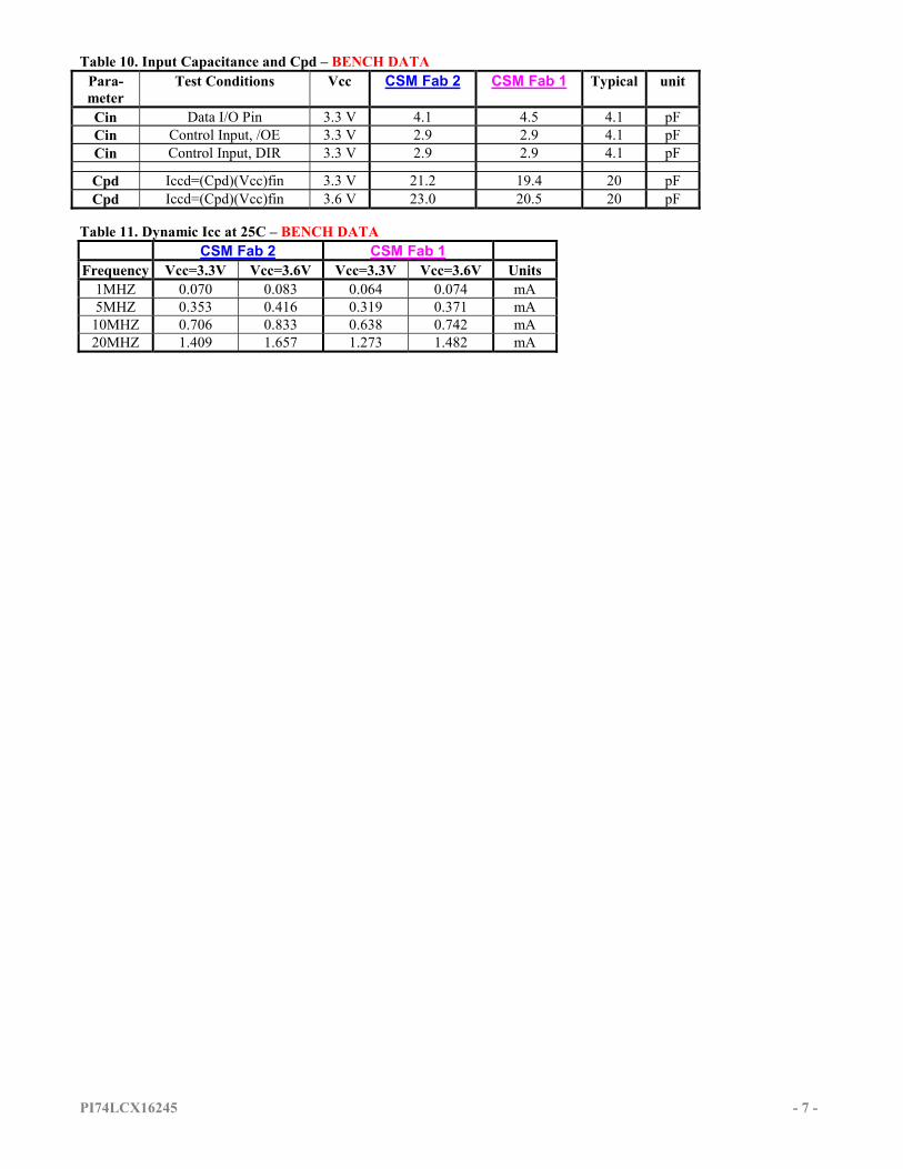
Table 10. Input Capacitance and Cpd – BENCH DATAPara-meter
Test Conditions Vcc CSM Fab 2 CSM Fab 1 Typical unit
Cin Data I/O Pin 3.3 V 4.1 4.5 4.1 pFCin Control Input, /OE 3.3 V 2.9 2.9 4.1 pFCin Control Input, DIR 3.3 V 2.9 2.9 4.1 pF
Cpd Iccd=(Cpd)(Vcc)fin 3.3 V 21.2 19.4 20 pFCpd Iccd=(Cpd)(Vcc)fin 3.6 V 23.0 20.5 20 pF
Table 11. Dynamic Icc at 25C – BENCH DATACSM Fab 2 CSM Fab 1
Frequency Vcc=3.3V Vcc=3.6V Vcc=3.3V Vcc=3.6V Units1MHZ 0.070 0.083 0.064 0.074 mA5MHZ 0.353 0.416 0.319 0.371 mA
10MHZ 0.706 0.833 0.638 0.742 mA20MHZ 1.409 1.657 1.273 1.482 mA