Embed Size (px)
Citation preview

EMI Filter & Rectifier
Boost PFC Power Stage
Bulk StorageLLC
Power StageBattery
42 V @ 9 A
Gate DriverUCC27714
LLC ControllerUCC25600
Bias ControlPFC Controller
UCC28180
Flyback Controller
UCC28722
LDOTLV70450
MCU
TL103
175 V - 265 V AC
1TIDU789C–March 2015–Revised January 2017Submit Documentation Feedback
Copyright © 2015–2017, Texas Instruments Incorporated
230-V, 400-W, 92% High Efficiency Battery Charger With PFC and LLC for36-V Power Tools Reference Design
TI Designs230-V, 400-W, 92% High Efficiency Battery Charger WithPFC and LLC for 36-V Power Tools Reference Design
TI DesignsTI Designs provide the foundation that you needincluding methodology, testing and design files toquickly evaluate and customize the system. TI Designshelp you accelerate your time to market.
Design Resources
TIDA-00355 Design FolderUCC28180 Product FolderUCC25600 Product FolderUCC27714 Product FolderUCC28722 Product FolderTLV70450 Product Folder
ASK Our E2E ExpertsWEBENCH® Calculator Tools
space
Design Features• 400-W Battery Charger With Front-End PFC and
Half-Bridge LLC Resonant Converter• Designed to Charge Wide Range of Batteries in the
Voltage Range of 20 to 42 V:– Li-Ion, Li-Poly, Ni-Cd and Lead-Acid
• Ideal Charger for 10-Cell Li-ion Battery Pack Usedin Industrial Power Tools
• Delivers up to 9 A of Continuous Charging Currentfor Fast Charging of Batteries
• Overall Efficiency of 92% at Full Charging Currentof 9 A and 230-V Input, Eliminating the Need forExternal Cooling
• High Power Factor > 0.99 and Meets PFCRegulations and Current THD as per IEC61000-3-2 Class A
• Very Low Standby Power of < 200 mW WhenBattery is Not Connected
• Small PCB Form Factor of 230 × 80 mm OffersPortability in Usage
• Provides Flexibility for Charge Profiling Through anAdditional External Microcontroller
• Charger is Protected for Overcurrent and ShortCircuit at Output Terminals Ensuring Safety Needs
• Meets the Requirements of Conducted EmissionsStandard – EN55011 Class A
Featured Applications• Cordless Power Tools• Cordless Garden Tools• Battery Chargers for
– Vacuum Cleaner– Robotic Mower– E-Bike, E-Cycle
An IMPORTANT NOTICE at the end of this TI reference design addresses authorized use, intellectual property matters and otherimportant disclaimers and information.

Introduction www.ti.com
2 TIDU789C–March 2015–Revised January 2017Submit Documentation Feedback
Copyright © 2015–2017, Texas Instruments Incorporated
230-V, 400-W, 92% High Efficiency Battery Charger With PFC and LLC for36-V Power Tools Reference Design
1 IntroductionPower tools are used in various industrial and household applications such as drilling, grinding, cutting,polishing, driving fasteners, various garden tools, and so on. The most common types of power tools useelectric motors while some use internal combustion engines, steam engines, or compressed air.
Power tools can be either corded or cordless (battery-powered). Corded power tools use the mains power(the grid power) to power up the AC or DC motors. The cordless tools use battery power to drive DCmotors. Most of the cordless tools use lithium-ion batteries, the most advanced in the industry. Lithium-ionbatteries have high energy density, low weight, and greater life. These batteries have relatively lowself-discharge (less than half that of nickel-based batteries) and can provide a very high current forapplications like power tools. Cordless tools use brushed or BLDC motors. The brushless motors are moreefficient and have less maintenance, low noise, and longer life.
This reference design is a complete battery charger for charging batteries used in battery-powered gardenand power tools rated up to 400 W. The design can be used to charge Li-ion and Li-poly chemistrybatteries with a voltage range from 36 to 42 V and maximum charging current of 9 A. The chargerprovides constant voltage and constant current controls with settable configuration as per chargingrequirements.
Power tool chargers have requirements of high efficiency at maximum charging current and low standbyrequirements when battery is not connected. This design demonstrates the high performance chargingpower stage in a small form factor (230 × 80 mm), operating from 175-V to 265-V AC and delivers up to9-A continuous current output to charge battery at greater than 90% efficiency. The design meets lowstandby power of < 200 mW when battery is not connected. The design also provides flexibility for batteryvoltage and current level setting for charge profiling, through an additional external microcontroller.
2 Key System Specifications
Table 1. Key System Specifications
PARAMETER SPECIFICATIONInput voltage range 175-V to 265-V AC
Output voltage 42 V ±2%, 0- to 9-A output currentOutput current 9 A ±5%, 20- to 42-V output voltage
Board form factor 230 × 80 mmExpected efficiency > 90% at 230 V and full load
Standby power < 500 mW at 230 V without battery connected on outputPower line harmonics As per IEC61000-3-2Conducted emissions As per EN55022 Class A
Auxiliary power for MCU 5 V at 100 mAOutput voltage ripple ±1 VOutput current ripple ±0.5 A

www.ti.com System Description
3TIDU789C–March 2015–Revised January 2017Submit Documentation Feedback
Copyright © 2015–2017, Texas Instruments Incorporated
230-V, 400-W, 92% High Efficiency Battery Charger With PFC and LLC for36-V Power Tools Reference Design
3 System DescriptionThe design is a 42-V, 400-W battery charger power supply with boost PFC pre-regulator using UCC28180as PFC controller and the main converter stage is realized using LLC configuration with UCC25600 asLLC controller and UCC27714 as gate driver. Internal auxiliary power supply for biasing controllers isimplemented using simple low cost flyback controller UCC28722. The system design is done to meet highefficiency, low EMI, and low standby power consumption specifications.
The charger is designed for input voltage range of 175-V to 265-V AC and used to charge batteries up to36 V at maximum current of 9 A. The design form factor (230 × 80 mm) is compact for the power level of400 W. The design has an operating efficiency of around 92% at full load, with voltage and currentregulation within ±3%.
The EMI filter at the front end of the circuit is designed to meet EN55022 Class-A conducted emissionlevels. This is followed by an active boost PFC stage operating in continuous conduction mode (CCM).This PFC stage regulates the DC bus voltage to 400 V, stabilized against line drop-outs with a bulkstorage capacitor. The isolated power stage of the charger is an LLC-resonant converter operating veryclose to resonant frequency at full load. The operation will move to above resonance with lighter loads inboth constant voltage and constant current regions of the charger. The constant current/constant voltage(CV/CC) feedback is achieved using the TL103W, which has an integrated dual op-amp and a 2.5-Vreference. The system is designed to meet below 200 mW of standby power when no battery isconnected. This goal is achieved by using a simple logic circuit that disables PFC and LLC power stageswhen battery is not present.
The ultra-low-cost flyback bias power supply is built using UCC28722 with a BJT as the switchingelement, resulting in very minimal cost impact. This bias power supply also provides the power needed foran external MCU, which can be optionally added as an add-on card to control the charging profile moreprecisely.
Various parameters of the design like regulation, efficiency, EMI signature, output ripple, startup, andswitching stresses were tested and documented.

EMI Filter & Rectifier
Boost PFC Power Stage
Bulk StorageLLC
Power StageBattery
42 V @ 9 A
Gate DriverUCC27714
LLC ControllerUCC25600
Bias ControlPFC Controller
UCC28180
Flyback Controller
UCC28722
LDOTLV70450
MCU
TL103
175 V - 265 V AC
Block Diagram www.ti.com
4 TIDU789C–March 2015–Revised January 2017Submit Documentation Feedback
Copyright © 2015–2017, Texas Instruments Incorporated
230-V, 400-W, 92% High Efficiency Battery Charger With PFC and LLC for36-V Power Tools Reference Design
4 Block Diagram
Figure 1. Block Diagram of 400-W Power Supply With PFC and LLC
4.1 Highlighted Products and Key Benefits for 400-W ChargerThe following are the highlighted products used in this reference design. Key features for selecting thedevices for this reference design are elucidated in the following sections. Complete details of thehighlighted devices can be referred in respective product datasheets.
4.1.1 UCC28180 – PFC ControllerTo implement the high performance, small form factor PFC design at 400-W power, the UCC28180 ispreferred controller as it offers series of benefits to address the next generation needs of low THD normsfor power tools.
The UCC28180 is an extremely high performance, CCM compact, 8-pin programmable frequency PFCcontroller. Its wide and programmable operating frequency provides flexibility to design at a high frequencyoptimizing the components. Its trimmed current loop circuits helps achieve less than 5% THD frommedium-to-full load (50 to 100%). Its reduced current sense threshold helps utilize a 50% smaller shuntresistor, resulting in lower power dissipation while maintaining low THD. Its integrated fast gate driver of2-A/1.5-A drive current eliminates the need for an external gate driver.
The UCC28180 also has a complete set of system protection features such as soft overcurrent,cycle-by-cycle current limit, output overvoltage protection, VCC UVLO, and open pin protections (ISENSE,VSENSE). These features greatly improve reliability and further simplifies the design.

www.ti.com Block Diagram
5TIDU789C–March 2015–Revised January 2017Submit Documentation Feedback
Copyright © 2015–2017, Texas Instruments Incorporated
230-V, 400-W, 92% High Efficiency Battery Charger With PFC and LLC for36-V Power Tools Reference Design
4.1.2 UCC25600 — LLC ControllerPower tool designs demand high frequency DC/DC conversion and high efficiency with small form-factor.The UCC25600 LLC controller is best fit for high wattage resonant power design as it offers all the keyadvantages for high performance and high efficiency DC/DC conversion at high power levels.
The UCC25600 is a simple 8-pin resonant mode controller designed for offline DC/DC applications. TheUCC25600 controller works in the LLC resonant half bridge topology and operates with zero voltageswitching (ZVS) to provide highly efficient voltage conversion operation, which nearly eliminates allswitching losses. This controller uses frequency modulation control has programmable dead-time controlwith a precision 50-ns set point accuracy and tight tolerances on the frequency, which reduces the needfor over-design saving system cost. The UCC25600 also has as complete set of system protectionfeatures such as overcurrent, over temperature and bias voltage OVP and UVLO, which greatly improvesreliability and further simplifies the design. Its unique programmable independent minimum and maximumswitching frequency settings prevents ZCS region operation and limits switching loss at light loadcondition. Its integrated burst mode operation helps maintain regulation at light load and no loadconditions.
4.1.3 UCC27714 — Gate DriverLLC converter implementation needs driving of two MOSFETs operated in half bridge configuration. TheUCC27714 offers all the key features as needed for half-bridge LLC implementation. Its high operatingvoltage range up to 600 V, and 4-A driving currents helps in simple implementation of LLC half-bridgedriver circuitry. Its best-in-class propagation delay (90 ns typ.) and delay matching (20 ns max.) betweenchannel helps in minimizing pulse distortion in high frequency LLC applications.
4.1.4 UCC28722 — Flyback ControllerTo achieve very low power consumption and optimize board space for the auxiliary power supply needs,the UCC28722 meets the bias supply needs. The main value of the UCC28722 solution is reduced totalcost. The design offers advantage of elimination of feedback components and its increasing switchingfrequency and increasing the VDD range aids in the reduction in size of power stage components. Inaddition, this solution allows to easily meet <50-mW standby power at the lowest system solution cost.

System Design Theory www.ti.com
6 TIDU789C–March 2015–Revised January 2017Submit Documentation Feedback
Copyright © 2015–2017, Texas Instruments Incorporated
230-V, 400-W, 92% High Efficiency Battery Charger With PFC and LLC for36-V Power Tools Reference Design
5 System Design TheoryThis reference design provides 400 W of power from a 230-V AC input with power factor correction. Thisdesign is intended for operation at country specific line voltages between 175-V to 265-V AC. TheUCC28180 controls a PFC boost front end, while the UCC25600 LLC-resonant half-bridge converts thePFC output to isolated 42 V and 9 A. The total system efficiency is 92% with a 230-V AC input and over90% with a 175-V AC input with full load. In addition, several protections are embedded into this designwhich includes input under-voltage protection and output short circuit protection.
Low EMI, high efficiency, high power factor, and a reliable power supply are the main focuses of thisdesign for targeted applications.
5.1 PFC Regulator Stage DesignPower factor correction shapes the input current of the power supply to maximize the real power availablefrom the mains. In addition, it is important to have PFC to comply with low harmonic (low THD) regulatoryrequirements such as IEC61000-3-2. Currently, two modes of operation have been widely utilized for PFCimplementations. For higher power circuits, the topology of choice is the boost converter operating in CCMand with average current mode control. For lower power applications, typically the critical conductionmode (CrCM) boost topology is used.
For high power levels such as 400 W, it is advisable to use CCM operation as it has lower peak and RMScurrents. Lower currents significantly reduce the stress in power MOSFET, diode, and inductor. Inaddition, the filtering is easier as the current through the boost inductor is more continuous. Finally, theswitching frequency remains constant for the CCM operation, so the boost inductor design and EMI filterdesigns are easier.
The UCC28180 operates at fixed frequency in CCM and requires minimal external components for highwattage PFC pre-regulator implementation. The design process and component selection for this designare illustrated below. All design calculations are available in the Excel® file "TIDA00355_PFC.xls"available at http://www.ti.com/tool/TIDA-00355.
5.1.1 Circuit Component Design
5.1.1.1 Design Parameters
Table 2. Design Parameters for PFC Power Stage Design
PARAMETER MIN TYP MAX UNITINPUT
VIN Input voltage 175 265 V ACfLINE Input frequency 47 63 Hz
OUTPUTVOUT Output voltage 397 V DCPOUT Output power 400 W
Line regulation 5%Load regulation 5%
PF Targeted power factor 0.99η Targeted efficiency 96%

OUTBST(min)
sw RIPPLE
BST(min)
V D (1 D)L
f I
397 0.377 (1 0.377)L 932 H
(98 1.02)
´ ´ -³
´
´ ´ -³ = m
´
OUT IN_RECTIFIED(min)(max)
OUT
(max)
V VDUTY
V
397 (1.414 175)DUTY 0.377
397
-
=
- ´
= =
RIPPLEIN
sw IN_RIPPLE
IN
IC
8 f V
1.02C 0.360 F
8 98 7.43
=´ ´
= = m´ ´
( )IN_RIPPLE RIPPLE _IN IN_RECTIFIED(min)
IN_RIPPLE
V V V
V 0.015 2 175 3.71 V
= D ´
= ´ ´ =
RIPPLE RIPPLE IN(max)
RIPPLE
I I I
I 0.3 ( 2 2.41) 1.02A
= D ´
= ´ ´ =
OUT(max)IN_RMS(max)
IN(min)
IN_RMS(max)
PI
V PF
400I 2.41 A
0.96 175 0.99
=h´ ´
= =´ ´
OUT(max)OUT(max)
OUT
OUT(max)
PI
V
400I 1.0 A
397
=
= =
www.ti.com System Design Theory
7TIDU789C–March 2015–Revised January 2017Submit Documentation Feedback
Copyright © 2015–2017, Texas Instruments Incorporated
230-V, 400-W, 92% High Efficiency Battery Charger With PFC and LLC for36-V Power Tools Reference Design
5.1.1.2 Current CalculationsThe input fuse, bridge rectifier, and input capacitor are selected based upon the input current calculations.First, determine the maximum average output current, IOUT(max):
(1)
The maximum input RMS line current, IIN_RMS(max), is calculated using the parameters from Table 2 and theefficiency and power factor initial assumptions:
(2)
space
(3)
space
Assuming ripple to be 1.5%,
(4)
The recommended value for the input X-capacitor can now be calculated:
(5)
A standard value 0.47-μF X2 film capacitor is used.
5.1.1.3 Boost InductorThe duty cycle of operation is a function of the rectified input voltage and will be continuously changingover the half-line cycle. The duty cycle, DUTY(max), can be calculated at the peak of the minimum inputvoltage:
(6)
The minimum value of the boost inductor is calculated based upon the acceptable ripple current, IRIPPLE, ata worst case duty cycle of 0.377:
(7)
The actual value of the boost inductor used is 1000 μH.

DIODE F _125C OUT(max) SW OUT RR
DIODE
P V I 0.5 f V Q
P 1.5 1.0 0.5 98 397 13 nC 1.75 W
= ´ + ´ ´ ´
= ´ + ´ ´ ´ =
COND SWP P 1.73 1.71 3.44 W+ = + =
2SW SW OUT IN(max) r f OSS OUT
2SW
P f 0.5 V I (t t ) 0.5 C V
P 98 0.5 397 3.4 (12 ns 6 ns) 0.5 68 pF 397 1.71 W
é ù= ´ ´ ´ + + ´ ´ë û
é ù= ´ ´ ´ ´ + + ´ ´ =ë û
2COND DS(on)DS _RMS
2COND
P I R
P 1.568 (0.7) 1.73 W
= ´
= ´ =
IN_RECTIFIED(min)OUT(max)DS _RMS
IN_RECTIFIED(min) OUT
DS _RMS
16 VPI 2
V 3 V
400 16 247I 2 1.57 A
247 3 397
´= ´ -
´ p ´
´æ ö= ´ - =ç ÷´ p ´è ø
OUT(max) HOLDUPOUT(min) 2 2
OUT OUT _HOLDUP(min)
OUT(min) 2 2
2 P tC
V V
2 400 20 msC 202 F
(397 280 )
´ ´³
-
´ ´³ = m
-
System Design Theory www.ti.com
8 TIDU789C–March 2015–Revised January 2017Submit Documentation Feedback
Copyright © 2015–2017, Texas Instruments Incorporated
230-V, 400-W, 92% High Efficiency Battery Charger With PFC and LLC for36-V Power Tools Reference Design
5.1.1.4 Output CapacitorThe output capacitor, COUT, is sized to meet holdup requirements of the converter. Assuming thedownstream converters require the output of the PFC stage to never fall below 280 V, VOUT_HOLDUP(min),during one line cycle, tHOLDUP = 1/fLINE(min), the minimum calculated value for the capacitor is:
(8)
The capacitor of 220 μF is selected, considering the capacitor tolerances.
5.1.1.5 Switching ElementThe drain to source RMS current, IDS_RMS through switching FET is calculated as
(9)
An AOTF12T50P MOSFET of 500 V/12 A is selected for the current design. Consider using a highervoltage rating FET (600 V/650 V) based on the design de-rating needs of the end equipment.
The conduction losses of the switch MOSFET in this design are estimated using the RDS(on) at 100°C,found in the device datasheet, and the calculated drain to source RMS current, IDS_RMS:
(10)
The switching losses are estimated using the rise time, tr, and fall time, tf, of the MOSFET gate, and theoutput capacitance losses (COSS).
(11)
Total FET losses:(12)
An appropriately sized heat sink is used for MOSFET.
5.1.1.6 Boost DiodeThe output diode should have a blocking voltage that exceeds the output over voltage of the converterand average current same as IOUT(max). BYV25FX-600, a 600-V/5-A diode, is selected as output diode.
The diode losses are estimated based upon the forward voltage drop, VF, at 125°C and the reverserecovery charge, QRR, of the diode:
(13)

PCL(max)PCL
SENSE
PCL
VI
R
0.438 VI 8.76 A
0.05
=
= =
2RSENSE SENSEIN_RMS(max)
2RSENSE
P I R
P 2.41 0.05 0.29 W
= ´
= ´ =
SOC(min)SENSE
L _PEAK(max)
SENSE
VR
I 1.1
0.259 VR 0.06
3.91 A 1.1
=´
= = W´
www.ti.com System Design Theory
9TIDU789C–March 2015–Revised January 2017Submit Documentation Feedback
Copyright © 2015–2017, Texas Instruments Incorporated
230-V, 400-W, 92% High Efficiency Battery Charger With PFC and LLC for36-V Power Tools Reference Design
5.1.1.7 Sense ResistorTo accommodate the gain of the non-linear power limit, the sense resistor, RSENSE, is sized such that ittriggers the soft overcurrent at 10% higher than the maximum peak inductor current using the minimumsoft over current threshold of the ISENSE pin, VSOC, of ISENSE equal to 0.265 V.
(14)
RSENSE selected is 0.05 Ω.
The power dissipated across the sense resistor, PRSENSE, must be calculated:
(15)
The peak current limit, PCL, protection feature is triggered when current through the sense resistor resultsin the voltage across RSENSE to be equal to the VPCL threshold. For a worst case analysis, the maximumVPCL threshold is used:
(16)
To protect the ISENSE pin from inrush-surge current, a 220-Ω resistor, RISENSE, is placed in series withthe ISENSE pin. A 1000-pF capacitor is placed close to the device to improve noise immunity on theISENSE pin.
VSENSEFB2
10 sC 82 pF
R
m= =
FB1 FB2OUT(uvp) UVD
FB2
OUT(uvp)
R RV V
R
9.96 M 127 kV (0.95 5) 377.3 V
127
æ ö+= ´ ç ÷
ç ÷è ø
W + W= ´ ´ =
W
FB1 FB2OUT(ovd) OVD
FB2
OUT(ovd)
R RV V
R
9.96 M 127 kV (1.05 5) 417 V
127 k
æ ö+= ´ ç ÷
ç ÷è ø
W + W= ´ ´ =
W
REF FB1
FB2
OUT REF
FB2
V RR
V V
5 V 9.96 MR 127 k
397 V 5 V
´=
-
´ W= = W
-
System Design Theory www.ti.com
10 TIDU789C–March 2015–Revised January 2017Submit Documentation Feedback
Copyright © 2015–2017, Texas Instruments Incorporated
230-V, 400-W, 92% High Efficiency Battery Charger With PFC and LLC for36-V Power Tools Reference Design
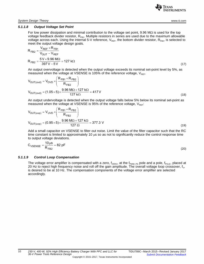
5.1.1.8 Output Voltage Set PointFor low power dissipation and minimal contribution to the voltage set point, 9.96 MΩ is used for the topvoltage feedback divider resistor, RFB1. Multiple resistors in series are used due to the maximum allowablevoltage across each. Using the internal 5-V reference, VREF, the bottom divider resistor, RFB2, is selected tomeet the output voltage design goals.
(17)
An output overvoltage is detected when the output voltage exceeds its nominal set-point level by 5%, asmeasured when the voltage at VSENSE is 105% of the reference voltage, VREF.
(18)
An output undervoltage is detected when the output voltage falls below 5% below its nominal set-point asmeasured when the voltage at VSENSE is 95% of the reference voltage, VREF:
(19)
Add a small capacitor on VSENSE to filter out noise. Limit the value of the filter capacitor such that the RCtime constant is limited to approximately 10 μs so as not to significantly reduce the control response timeto output voltage deviations.
(20)
5.1.1.9 Control Loop CompensationThe voltage error amplifier is compensated with a zero, fZERO, at the fPWM_PS pole and a pole, fPOLE, placed at20 Hz to reject high frequency noise and roll off the gain amplitude. The overall voltage loop crossover, fV,is desired to be at 10 Hz. The compensation components of the voltage error amplifier are selectedaccordingly.

www.ti.com System Design Theory
11TIDU789C–March 2015–Revised January 2017Submit Documentation Feedback
Copyright © 2015–2017, Texas Instruments Incorporated
230-V, 400-W, 92% High Efficiency Battery Charger With PFC and LLC for36-V Power Tools Reference Design
5.2 LLC Converter Stage DesignIncreased demands for high power density power supplies have resulted in the increase in switchingfrequency of the converters designed. While component sizes tend to decrease with an increase in theswitching frequency, device switching losses (which are proportional to frequency) have significantlyincreased contributing significant efficiency loss. Resonant converters use soft-switching techniques toalleviate switching loss problems and attain high efficiencies. Furthermore, soft-switching helps attain lowlosses during light load conditions, very low device stress, and reduced EMI.
The three main classes of resonant converters are series resonant converter (SRC), parallel resonantconverter (PRC) and a combination of the two, the series-parallel resonant converter (SPRC). Amongthese the simplest and most popular resonant converter is the LLC series resonant converter.
The LLC resonant converter is based on the SRC. By using the transformer magnetizing inductor,zero-voltage switching can be achieved over a wide range of input voltage and load. As a result of multipleresonances, zero-voltage switching can be maintained even when the switching frequency is higher orlower than the resonant frequency. The converter achieves the best efficiency when operated close to itsresonant frequency at a nominal input voltage. As the switching frequency is lowered, the voltage gain issignificantly increased. This allows the converter to maintain regulation when the input voltage falls low.These features make the converter ideally suited to operate from the output of a high-voltage boost PFCpre-regulator, allowing it to hold up through brief periods of ac line-voltage dropout.
The UCC25600 is low-pin count and low cost LLC controller and requires minimal components to deliveroptimum system performance. In addition, controller delivers complete system protection functionsincluding overcurrent, UVLO, bias supply OVP and over temperature protection. The design process andcomponent selection for this design are illustrated below. All design calculations are available in the Excelfile "TIDA00355_LLC.xlsx" available at http://www.ti.com/tool/TIDA-00355.
5.2.1 Design Parameters
Table 3. Design Parameters for LLC Power Stage Design
PARAMETER MIN TYP MAX UNITINPUT
VINDC Input voltage 375 397 410 V DCOUTPUT
VOUT Output voltage 42 V DCPLIMIT Output power limit 400 WPOUT Max output power 390 Wfswnom Nominal switching frequency 98.5 kHz
Line regulation 1 %Load regulation 1 %
PF Targeted power factor 0.99η Targeted efficiency 0.95

Converter Specifications
Magnetizing Inductance
Resonant Inductor
Resonant Capacitor
Calculate R
Choose L and Q
e
n e
nChange L and Qe
No
Are ValuesWithin
Limits?MM
g_max
ff
g_min
n_max
n_min
Yes
Check M and fAgainst Graph
g n
0 0.5 1 1.5
f = 1.02
Normalized Frequency (f
n_max
n)
Gain
, (M
g)
1.9
1.7
1.5
1.3
1.1
0.9
0.7
0.5
M = 1.3g_max
Q = 0e
Q = 0.47e
M = 0.99g_min
Q = 0.52e
f = 0.65
L
n_min
= 3.5n
0.15 1.150.950.750.550.35
Quality Factor (Qe)
Att
ain
ab
le P
ea
k G
ain
(M
g_ap
)
3.0
2.8
2.6
2.4
2.2
2.0
1.8
1.6
1.4
1.2
1.0
L = 3.5 byInterpolationM = 1.56Q = 0.45
n
g_ap
e
L = 5M = 1.2Q = 0.5
n
g_ap
e
L = 1.5n
L = 3.0n
L = 1.5L = 2.0L = 3.0L = 4.0L = 5.0L = 6.0L = 8.0L = 9.0
n
n
n
n
n
n
n
n
in
o
Vn
2V=
o _ ming _ min
in _ max
n VM
V / 2
´=
o _ maxg _ max
in _ min
n VM
V / 2
´=
m n rL L L= ´
( )r 2
sw r
1L
2 f C=
p ´
rsw e e
1C
2 f R Q=
p
22 2o
e L2 2out
V8 n 8 nR R
P
´ ´= ´ = ´
p p
System Design Theory www.ti.com
12 TIDU789C–March 2015–Revised January 2017Submit Documentation Feedback
Copyright © 2015–2017, Texas Instruments Incorporated
230-V, 400-W, 92% High Efficiency Battery Charger With PFC and LLC for36-V Power Tools Reference Design
5.2.2 Design Steps
5.2.2.1 Flow Chart for LLC Resonant-Network Design
Figure 2. Flow Chart for LLC Resonant-Network Design
O _ max Fg _ max
DCIN_ min
g _ max
V VM n
V / 2
42 V (1 1%) 0.7 VM 5 1.15
375 V / 2
æ ö+= ´ ç ÷
ç ÷è ø
æ ö´ + += ´ =ç ÷
è ø
O _ min Fg _ min
DCIN_ max
g _ min
V VM n
V / 2
42 V (1 1%) 0.7 VM 5 1.03
410 V / 2
æ ö+= ´ ç ÷
ç ÷è ø
æ ö´ - += ´ =ç ÷
è ø
( ) ( )DCIN_NOM
O
V / 2 397 / 2n 4.72 5
V 42= = = Þ
DCIN_NOMg g
O
V / 2n M M 1
V= ´ =M
www.ti.com System Design Theory
13TIDU789C–March 2015–Revised January 2017Submit Documentation Feedback
Copyright © 2015–2017, Texas Instruments Incorporated
230-V, 400-W, 92% High Efficiency Battery Charger With PFC and LLC for36-V Power Tools Reference Design
5.2.2.2 Determine Transformer Turns Ratio (n)The transformer turns ratio is determined by Equation 21:
(21)
Where Mg is the voltage gain.
From the specifications, the nominal values for input voltage and output voltage are 397 V and 42 V,respectively, so the turns-ratio can be calculated as
(22)
5.2.2.3 Determine Mg_min and Mg_max
Mg_min and Mg_max can be determined by using Equation 23 and Equation 24, respectively:
(23)
In these calculations, 1% is used to adjust output voltage from the line and load regulation. VF = 0.7 V isassumed for the secondary side diode’s forward-voltage drop.
(24)
To keep operation within the inductive region with an overload current capability of 110%, Mg_max isincreased to 1.15 × 110% = 1.26.

m n r
m
L L L
L 5 69 H 345 H
= ´
= ´ m = m
r 2o r
r 2
1L
(2 f ) C
1L 69 H
(2 98 k ) 38.2 nF
=´ p ´ ´
= = m´ p ´ W ´
r
e o e
r
1C
2 Q f R
1C 38.2 nF
2 0.45 98 k 94.6
=
´ p ´ ´ ´
= =
´ p ´ ´ ´
2O
e 2O
2
e 2
V8 nR
I
8 5 42R 94.6
9
æ ö´= ´ ç ÷
ç ÷p è ø
´ æ ö= ´ = Wç ÷
è øp
0.15 1.150.950.750.550.35
Quality Factor (Q )e
Att
ain
ab
le P
eak G
ain
(M
)g
_a
p
3.0
2.8
2.6
2.4
2.2
2.0
1.8
1.6
1.4
1.2
1.0
L = 3.5 byInterpolationM = 1.56Q = 0.45
n
g_ap
e
L = 5M = 1.2Q = 0.5
n
g_ap
e
L = 1.5n
L = 3.0n
L = 1.5L = 2.0L = 3.0L = 4.0L = 5.0L = 6.0L = 8.0L = 9.0
n
n
n
n
n
n
n
n
System Design Theory www.ti.com
14 TIDU789C–March 2015–Revised January 2017Submit Documentation Feedback
Copyright © 2015–2017, Texas Instruments Incorporated
230-V, 400-W, 92% High Efficiency Battery Charger With PFC and LLC for36-V Power Tools Reference Design
5.2.2.4 Select Ln and Qe
From Figure 3, if the values Ln = 5 and Qe = 0.45 are selected, the corresponding Mg_ap = 1.3, which isgreater than Mg_max = 1.26. Any other Ln curve which is not shown in Figure 3, for example Ln = 3.5, can beobtained by interpolating the curves of Ln = 3 and Ln = 4.
Figure 3. Peak Gain Curves
5.2.2.5 Determine Equivalent Load Resistance (Re) of Resonant NetworkRe is determined from Equation 25. At full load,
(25)
5.2.2.6 Determine Resonant Circuit ParametersA switching frequency of 98 kHz is selected initially for the series resonant frequency. The resonantcircuit’s parameters at full load are determined from Equation 26, Equation 27, and Equation 28.
(26)
space
(27)
space
(28)
r r
e
e
e
L / CQ
R
75 / 39 nQ 0.463
94.6
=
m= =
m
n
r
n
LL
L
400 HL 5.33
75 H
=
m= =
m
o
r r
o
1f
2 L C
1f 93 kHz
2 39 nF 75 F
=
´ p ´ ´
= =
´ p ´ ´ m
www.ti.com System Design Theory
15TIDU789C–March 2015–Revised January 2017Submit Documentation Feedback
Copyright © 2015–2017, Texas Instruments Incorporated
230-V, 400-W, 92% High Efficiency Battery Charger With PFC and LLC for36-V Power Tools Reference Design
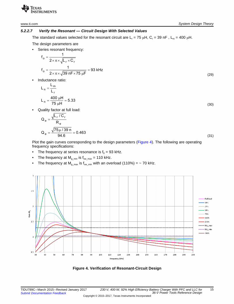
5.2.2.7 Verify the Resonant — Circuit Design With Selected ValuesThe standard values selected for the resonant circuit are Lr = 75 μH, Cr = 39 nF , Lm = 400 μH.
The design parameters are• Series resonant frequency:
(29)• Inductance ratio:
(30)• Quality factor at full load:
(31)
Plot the gain curves corresponding to the design parameters (Figure 4). The following are operatingfrequency specifications:• The frequency at series resonance is f0 = 93 kHz.• The frequency at Mg_min is fsw_max = 110 kHz.• The frequency at Mg_max is fsw_min with an overload (110%) = ~ 70 kHz.
Figure 4. Verification of Resonant-Circuit Design

sec_ avg sec
sec_ avg
2I I
2I 11 A 4.95 A
= ´
p
= ´ =
p
sec_ sw sec
sec_ sw
2I I
2
2I 11 A 7.8 A
2
= ´
= ´ =
sec pri
sec
I n I
I 5 2.2 A 11 A
= ´
= ´ =
22r m pri
2 2r
I I I
I 2.2 1.08 2.45 A
= +
= + =
om
m
m
n VI 0.901
L
5 42I 0.901 1.08 A
2 70 kHz 400 H
æ ö´= ´ ç ÷
ç ÷w´è ø
æ ö´= ´ =ç ÷´ p ´ ´ mè ø
Opri
pri
I 110%I
n2 2
9 1.1I 1.11 2.2 A
5
´æ öp= ´ ç ÷ç ÷
è ø
´æ ö= ´ =ç ÷
è ø
System Design Theory www.ti.com
16 TIDU789C–March 2015–Revised January 2017Submit Documentation Feedback
Copyright © 2015–2017, Texas Instruments Incorporated
230-V, 400-W, 92% High Efficiency Battery Charger With PFC and LLC for36-V Power Tools Reference Design
5.2.2.8 Determine the Primary-Side CurrentsThe primary-side RMS load current (Ipri) with a 110% overload is determined from Equation 32:
(32)
The RMS magnetizing current (Im) at fsw_min = 70 kHz is determined from Equation 33:
(33)
The resonant circuit’s current (Ir) is determined from Equation 34:
(34)
This is also the transformer’s primary winding current at fsw_min.
5.2.2.9 Determine the Secondary-Side CurrentsThe total secondary-side RMS load current is the current referred from the primary-side current (Ipri) to thesecondary side:
With a 110% overload,
(35)
Because the transformer’s secondary side has a center-tapped configuration, this current is equally splitinto two transformer windings on the secondary side. The current of each winding is then calculated as
(36)
The corresponding half-wave average current is
(37)
22Cr _RMS DCIN_ max Cr
2 2Cr _RMS
V (V / 2) V
V (410 / 2) 145 251 V
= +
= + =
r
Cr
r
Cr
IV
C
2.45 AV 143 V
2 70 kHz 39 nF
=
w´
= =
p ´ ´
Lr r r
Lr
V L I
V 2 110 kHz 75 H 2.45 A 127 V
= w´ ´
= ´ p ´ ´ m ´ =
www.ti.com System Design Theory
17TIDU789C–March 2015–Revised January 2017Submit Documentation Feedback
Copyright © 2015–2017, Texas Instruments Incorporated
230-V, 400-W, 92% High Efficiency Battery Charger With PFC and LLC for36-V Power Tools Reference Design
5.2.2.10 Select the TransformerThe transformer can be built or purchased from a catalog. The specifications for this example are:• Turns ratio (n): 5• Primary terminal voltage: 450-V AC• Primary winding’s rated current, Iwp: 2.5 A• Secondary terminal voltage: 100-V AC• Secondary winding’s rated current, Iws: 7.8 A (center-tapped configuration)• Frequency at no load: 110 kHz• Frequency at full load: 70 kHz• Insulation between primary and secondary sides: IEC60950 reinforced insulation
5.2.2.11 Select the Resonant InductorThe inductor can be built or purchased from a catalog, with these specifications:• Series resonant inductance, Lr: 75 μH• Rated current, ILr: 2.5 A• Terminal AC voltage:
(38)• Frequency range: 70 to 110 kHz
5.2.2.12 Select the Resonant CapacitorThe resonant capacitor (Cr) must have a low dissipation factor (DF) due to its high-frequency,high-magnitude current. Capacitors often used for LLC converters are made with metalized polypropylenefilm. These capacitors present very low DF and are capable of handling high-frequency current.
Before a capacitor is selected, its voltage rating has to be de-rated with regard to the switching frequencyin use.
The selected capacitor (Cr) must meet these additional specifications:• Rated current, ICr: 2.5 A• AC voltage across capacitor
(39)• RMS voltage:
(40)
sec_ avg sec
sec_ avg
2I I
2I 11 A 4.95 A
= ´
p
= ´ =
p
DCIN_ maxdiode
V / 2V 2
2= ´
deadt 242 ns³
deadt 16 315 pF 120 kHz 400 H³ ´ ´ ´ m
dead eq sw mt 16 C f L³ ´ ´ ´
DS _RMS rI I 2.45 A= =
DS INDC _ max
DS
V 1.2 V
V 1.2 410 492 V 500 V
= ´
= ´ = Þ
System Design Theory www.ti.com
18 TIDU789C–March 2015–Revised January 2017Submit Documentation Feedback
Copyright © 2015–2017, Texas Instruments Incorporated
230-V, 400-W, 92% High Efficiency Battery Charger With PFC and LLC for36-V Power Tools Reference Design
5.2.2.13 Select the Primary Side MOSFETsEach MOSFET sees the input voltage as its maximum applied voltage:
(41)
Each MOSFET conducts half of the resonant network’s current in steady state after the resonantcapacitor’s voltage has been established. However, during the initial start-up and transient, the current ineach MOSFET can be as high as the resonant current (Ir) with a 110% overload:
(42)
MOSFET switching losses are minimized by ZVS; therefore, the conduction losses from the MOSFETsmay become the main concern for the design. This suggests that MOSFETs with a low RDS_on should beused.
The MOSFET selected for this design is FDPF18N50, a 500-V/18-A device. Consider using a highervoltage rating FET (600 V/650 V) based on the design de-rating needs of the end equipment.
5.2.2.14 Select Dead Time to Ensure ZVS OperationThe condition under which the converter has sufficient switching dead time for ZVS is described byEquation 43:
(43)
Ceq is mainly from the MOSFET Cds. The MOSFET Cds for FDPF18N50 is approximately 315 pF.
(44)
5.2.2.15 Select Diode RectifierThe rectifier voltage rating of the diode is determined as
(45)
The current rating of the diodes is determined as
(46)
The rectifier diode selected for this design is the STPS20M120.

O _ pk _ pk O _ pk _ pkmax
rect _ pkO
max
V VESR
II 2
4
0.12 VESR 8.5 m
92
= =pæ ö
´ ´ç ÷è ø
= = Wpæ ö
´ç ÷è ø
22
Co _RMS O O
Co _RMS O
I I I2
I 0.482 I 0.482 9.0 4.34 A
pæ ö= ´ -ç ÷
è ø
= ´ = ´ =
www.ti.com System Design Theory
19TIDU789C–March 2015–Revised January 2017Submit Documentation Feedback
Copyright © 2015–2017, Texas Instruments Incorporated
230-V, 400-W, 92% High Efficiency Battery Charger With PFC and LLC for36-V Power Tools Reference Design
5.2.2.16 Output Filter DesignIn an LLC converter, the output filter may consist of capacitors alone instead of the LC filter seen in mostpulse-width-modulated converters, although a small second-stage LC filter can be an option. If the filterhas only capacitors, they should be chosen to allow conduction of the rectifier current through all ACcomponents.
For the load current (Io), the capacitor’s RMS current rating at about 100 kHz is calculated as
(47)
Usually, a single capacitor will not allow such a high RMS current, so several capacitors connected inparallel are often used and may offer a lower profile.
The ripple voltage is a function of the amount of AC current that flows in and out of the capacitors witheach switching cycle, multiplied by the capacitors’ ESR. Because all electric current, including the load’sDC current, can be assumed to flow in and out of the filter capacitors, this is a very good estimate of theripple voltage. To meet the specification for a 120-mV ripple voltage, the maximum ESR should be
(48)
Capacitance value is selected based on• Voltage rating: 63 V• Ripple-current rating: 4.5 A at 100 kHz• ESR: < 8.5 mΩ
The design uses four numbers of C3225X7S2A475M200AB (4.7 µF, 100 V) capacitors to meet the RMSrating.

f max
f max f min
f max
2.5 VR
I I
2.5 VR 0.54 mA
5.46 mA 0.86 mA
=
-
= =
-
f min
f min
f min
2.5 VR
I
2.5 VR 2.9 k
0.86 mA
=
= = W
f min
6 nsI 0.86 mA
1150 ns
2 70 kHz
= =æ ö
-ç ÷´è ø
f min
min
6 nsI
1150 ns
2 f
=æ ö
-ç ÷ç ÷´è ø
f max
6 nsI 5.46 mA
1150 ns
2 400 kHZ
= =æ ö
-ç ÷´è ø
f max
max
6 nsI
1150 ns
2 f
=æ ö
-ç ÷ç ÷´è ø
d dt
td
t 20 ns R 24 ns / k
350 20R 13.75 k
24
= + ´ W
-= = W
System Design Theory www.ti.com
20 TIDU789C–March 2015–Revised January 2017Submit Documentation Feedback
Copyright © 2015–2017, Texas Instruments Incorporated
230-V, 400-W, 92% High Efficiency Battery Charger With PFC and LLC for36-V Power Tools Reference Design
5.2.3 Components for UCC25600 ControllerEach of the components for the controller is selected as per the datasheet recommendations. The valuescan also be obtained from "TIDA00355_LLC.xls" available at http://www.ti.com/tool/TIDA-00355.
5.2.3.1 Dead TimeA dead time of 350 ns is selected as per Equation 49. The resistor needed at the DT pin to GND iscalculated with
(49)
A standard value of 13.7 kΩ is used.
5.2.3.2 Frequency Setting ResistorThe frequency limiting resistor can be calculated based on following equations:
(50)
A maximum frequency of 400 kHz is selected to enable burst mode of operation for light load conditions.Burst mode gets enabled when the control loop demands a switching frequency higher than 350 kHz.
(51)
(52)
With a minimum frequency of 65 kHz selected considering overload conditions,
(53)
Minimum frequency limiting resistor is calculated as
(54)
Selected value is 2.34 kΩ, to avoid lower frequency operation.
(55)
pp min
p
10C
R f
10C 26 nF
5.49 k 70 k
=
´
= =
´
sp
Crpk
p
RR
V
316 kR 5.45 k
182
= ´ p
= ´ p = W
s
s min
s
10C
R f
10C 0.45 nF
316 k 70 kHz
=
´
= =
´
2Crpk
sr s
CrCrpk
2
s
VR
2 P
4 V 4 143V 182 V
182R 331 k
2 0.05 W
=´
´ ´= = =
p p
= = W´
R s C s
R pC p C rD 1
D 2
L m
TR
L r
From half bridge
To OC
www.ti.com System Design Theory
21TIDU789C–March 2015–Revised January 2017Submit Documentation Feedback
Copyright © 2015–2017, Texas Instruments Incorporated
230-V, 400-W, 92% High Efficiency Battery Charger With PFC and LLC for36-V Power Tools Reference Design
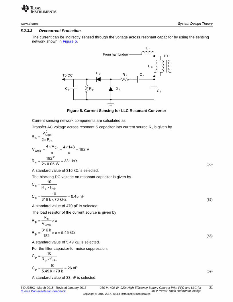
5.2.3.3 Overcurrent ProtectionThe current can be indirectly sensed through the voltage across resonant capacitor by using the sensingnetwork shown in Figure 5.
Figure 5. Current Sensing for LLC Resonant Converter
Current sensing network components are calculated as
Transfer AC voltage across resonant S capacitor into current source Rs is given by
(56)
A standard value of 316 kΩ is selected.
The blocking DC voltage on resonant capacitor is given by
(57)
A standard value of 470 pF is selected.
The load resistor of the current source is given by
(58)
A standard value of 5.49 kΩ is selected.
For the filter capacitor for noise suppression,
(59)
A standard value of 33 nF is selected.

System Design Theory www.ti.com
22 TIDU789C–March 2015–Revised January 2017Submit Documentation Feedback
Copyright © 2015–2017, Texas Instruments Incorporated
230-V, 400-W, 92% High Efficiency Battery Charger With PFC and LLC for36-V Power Tools Reference Design
5.2.4 CC-CV FeedbackThe charging cycle of a Li-ion battery (or a similar battery) consists of a constant-current phase and aconstant-voltage phase. To reflect this behavior, this reference design contains two feedback paths,implemented with the highly integrated op-amp, TL103W. The TL103W integrates two precision op-ampsand a 2.5-V voltage reference — both of which ease out CC-CV control loop circuitry implementation.
The first feedback path regulates the voltage in the constant-voltage phase through the resistor dividernetwork formed by R27 and R46. The voltage obtained is compared with the internal reference of 2.5 V toregulate the loop.
The second feedback path regulates the current in the constant-current phase once the output currentreaches the output-current limit. The output-current limit is set by the value of the two parallel shuntresistors, R18 and R20. These resistors determine the current regulation set point and must beadequately rated in terms of power dissipation. The voltage across those resistors is compared with thereference set by R29 and R30.
The designer can change the output voltage by changing the value of R27 and R46. The designer canchange the output current limit by changing R18 and R20. If the temperature dissipated by the shuntresistors is too high, the designer may either increase the number of shunt resistors in parallel or tune thevoltage reference set by R29 and R30.
5.3 Bias Power SupplyThe PFC, LLC controllers, and gate driver need auxiliary power supply for start-up and operation. Anauxiliary power supply of 1.3 W is produced on board by using a quasi-resonant/discontinuous currentmode flyback controller with primary-side control, the UCC28722. This controller offers a low part countand relatively low-cost solution eliminating the need for opto-coupler and TL431 feedback circuitry. Inaddition, quasi-resonant topology ensures high efficiency, optimizing the losses.
The converter is powered from the output of the PFC pre-regulator stage and must be able to start upprior to the PFC stage being operational. For this reason, the circuit is designed to operate over a wideinput voltage, 100-V to 450-V DC. The flyback transformer has two output windings, which are isolated toeach other and supply different circuits on the board. The design specifications of these outputs areshown in Table 4:
Table 4. Design Specifications of Bias Supply
PARAMETER SPECIFICATIONInput voltage range 160-V AC to 265-V AC
Output voltages
13 V at 50 mAAll circuits on the primary side: PFC controller, LLC controller, gate driver UCC277146.5 V at 100 mAInternal circuit needs and external microcontroller power
Design of power stage components (flyback transformer, output filter capacitor, and feedback circuitry) isexplained in detail in the UCC28722/UCC28720 application report (SLUA700).
All design calculations are available in the Excel file “TIDA00355_Bias_Supply.xlsx” available athttp://www.ti.com/tool/TIDA-00355.

www.ti.com Getting Started Hardware
23TIDU789C–March 2015–Revised January 2017Submit Documentation Feedback
Copyright © 2015–2017, Texas Instruments Incorporated
230-V, 400-W, 92% High Efficiency Battery Charger With PFC and LLC for36-V Power Tools Reference Design
6 Getting Started Hardware
6.1 Test ConditionsInput conditions:• VIN: 175-V to 265-V AC• Set the input current limit to 3.5 A
Output:• Variable simulated battery load, 20 to 42 V, 0 to 9 A
6.2 Equipment Needed• Isolated AC source• Single-phase power analyzer• Digital oscilloscope• Multi-meters• Electronic load to simulate battery
6.3 Procedure
1. Connect input terminals (connector J1) of the reference board to the AC power source.2. Connect output terminals (connector J3) to electronic load, maintaining correct polarity.3. Set the minimum load of about 100 mA, and minimum voltage of 25 V.4. Gradually increase the input voltage from 0 V to turn on voltage of 175-V AC.5. Turn on the load to apply voltage to the output terminals of the charger.6. Observe the startup conditions for smooth switching waveforms.

Test Data www.ti.com
24 TIDU789C–March 2015–Revised January 2017Submit Documentation Feedback
Copyright © 2015–2017, Texas Instruments Incorporated
230-V, 400-W, 92% High Efficiency Battery Charger With PFC and LLC for 36-VPower Tools Reference Design
7 Test Data
7.1 Efficiency and Regulation
7.1.1 Standby Power With Battery DisconnectedThe standby power was noted at various input voltages with no load conditions (that is, when the batteryis disconnected). The results are tabulated in Table 5 and are in accordance with the target specifications.
Table 5. Standby Test Results
AC INPUT INPUT POWER (BATTERY DISCONNECTED)175-V AC 140 mW230-V AC 150 mW265-V AC 170 mW
7.1.2 Performance Data of Charger
Table 6. At 175-V AC
VIN (VAC) PIN (W) PF ITHD VO (V) IO (A) PO (W) EFFICIENCY(%)
175 0.14 – – 0.00 0.000 0.00 0.00175 2.80 – – 42.37 0.000 0.00 0.00175 8.59 0.804 44.7 42.35 0.100 4.24 49.31175 27.28 0.939 23.1 42.35 0.500 21.18 77.63175 50.74 0.977 15.8 42.35 1.000 42.35 83.46175 141.90 0.997 1.3 42.33 3.000 127.00 89.50175 233.70 0.998 2.0 42.32 5.000 211.58 90.53175 327.20 0.999 3.2 42.30 7.000 296.10 90.50175 422.30 0.990 13.9 42.28 9.000 380.55 90.11175 429.80 0.989 14.9 42.28 9.150 386.90 90.02175 410.90 0.997 7.2 40.00 9.210 368.40 89.66175 363.00 0.998 5.9 35.00 9.220 322.70 88.90175 314.80 0.998 4.5 30.00 9.210 276.30 87.77175 266.50 0.998 3.5 25.00 9.200 230.00 86.30175 218.30 0.998 2.5 20.00 9.200 184.00 84.29
Table 7. At 230-V AC
VIN (VAC) PIN (W) PF ITHD VO (V) IO (A) PO (W) EFFICIENCY(%)
230 0.17 – – 0.00 0.000 0.00 0.00230 1.90 – – 42.39 0.000 0.00 0.00230 8.77 0.723 54.1 42.37 0.100 4.24 48.31230 26.82 0.907 24.3 42.37 0.500 21.18 78.98230 49.77 0.942 21.1 42.36 1.000 42.36 85.11230 140.30 0.992 2.8 42.34 3.000 127.03 90.54230 231.20 0.996 1.9 42.32 5.000 211.62 91.53230 323.60 0.997 2.7 42.30 7.000 296.13 91.51230 416.00 0.994 9.4 42.28 9.000 380.56 91.48230 423.30 0.993 9.9 42.28 9.180 388.10 91.69230 405.10 0.997 4.0 40.00 9.250 370.00 91.34
Output Current (A)
Effi
cien
cy (
%)
0 2 4 6 8 100
20
40
60
80
100
D004
Vi=175 VVi=230 VVi=265 V
Output Current (A)
Effi
cien
cy (
%)
15 20 25 30 35 40 4570
75
80
85
90
95
D005
Vi = 175 VVi = 230 VVi = 265 V
www.ti.com Test Data
25TIDU789C–March 2015–Revised January 2017Submit Documentation Feedback
Copyright © 2015–2017, Texas Instruments Incorporated
230-V, 400-W, 92% High Efficiency Battery Charger With PFC and LLC for36-V Power Tools Reference Design
Table 7. At 230-V AC (continued)
VIN (VAC) PIN (W) PF ITHD VO (V) IO (A) PO (W) EFFICIENCY(%)
230 358.30 0.997 3.3 35.00 9.245 323.58 90.31230 310.70 0.997 2.7 30.00 9.235 277.05 89.17230 263.20 0.996 2.4 25.00 9.230 230.75 87.67230 215.80 0.996 2.0 20.00 9.220 184.40 85.45
Table 8. At 265-V AC
VIN (VAC) PIN (W) PF ITHD VO (V) IO (A) PO (W) EFFICIENCY(%)
265 0.18 – – 0.00 0.000 0.00 0.00265 2.00 – – 42.39 0.000 0.00 0.00265 8.33 0.625 97.0 42.37 0.100 4.24 50.86265 26.29 0.880 34.0 42.36 0.500 21.18 80.57265 49.22 0.911 23.0 42.36 1.000 42.36 86.06265 138.64 0.987 8.1 42.34 3.000 127.02 91.62265 229.60 0.994 2.4 42.32 5.000 211.61 92.16265 321.40 0.996 2.6 42.30 7.000 296.11 92.13265 413.90 0.996 3.6 42.28 9.000 380.51 91.93265 422.30 0.995 6.3 42.26 9.180 387.93 91.86265 404.20 0.997 3.2 40.00 9.250 370.00 91.54265 357.30 0.996 2.9 35.00 9.245 323.58 90.56265 309.90 0.996 2.6 30.00 9.235 277.05 89.40265 262.30 0.995 2.4 25.00 9.230 230.75 87.97265 215.10 0.993 2.5 20.00 9.220 184.40 85.73
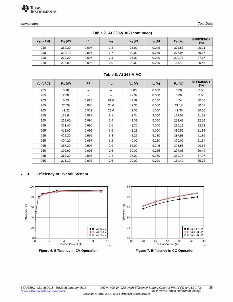
7.1.3 Efficiency of Overall System
Figure 6. Efficiency in CV Operation Figure 7. Efficiency in CC Operation

Output Current (A)
Effi
cien
cy (
%)
0 2 4 6 8 100
20
40
60
80
100
D002Output Current (A)
Effi
cien
cy (
%)
15 20 25 30 35 40 4570
75
80
85
90
95
100
D003
Output Current (A)
Eff
icie
nc
y (
%)
0 0.2 0.4 0.6 0.8 1 1.20
20
40
60
80
100
D001
175 VAC230 VAC265 VAC
Output Current (A)
Out
put V
olta
ge (
V)
0 1 2 3 4 5 6 7 8 9 1020
25
30
35
40
45
D005
Test Data www.ti.com
26 TIDU789C–March 2015–Revised January 2017Submit Documentation Feedback
Copyright © 2015–2017, Texas Instruments Incorporated
230-V, 400-W, 92% High Efficiency Battery Charger With PFC and LLC for36-V Power Tools Reference Design
7.1.4 Load Regulation
Figure 8. Load Regulation
7.1.5 Efficiency of PFC Power Stage
Figure 9. PFC Power Stage Efficiency
7.1.6 Efficiency of LLC Power Stage
Figure 10. LLC Converter Efficiency in CV Operation Figure 11. LLC Converter Efficiency in CC Operation

www.ti.com Test Data
27TIDU789C–March 2015–Revised January 2017Submit Documentation Feedback
Copyright © 2015–2017, Texas Instruments Incorporated
230-V, 400-W, 92% High Efficiency Battery Charger With PFC and LLC for36-V Power Tools Reference Design
7.2 Waveforms
7.2.1 PFC Switching Waveforms
Figure 12. VIN = 175-V AC, Full Load
NOTE: Red trace: Drain voltage, 100 V/div; Yellow trace: Drain current, 5 A/div
Figure 13. VIN = 265-V AC, Full Load
NOTE: Red trace: Drain voltage, 100 V/div; Yellow trace: Drain current, 5 A/div
Test Data www.ti.com
28 TIDU789C–March 2015–Revised January 2017Submit Documentation Feedback
Copyright © 2015–2017, Texas Instruments Incorporated
230-V, 400-W, 92% High Efficiency Battery Charger With PFC and LLC for36-V Power Tools Reference Design
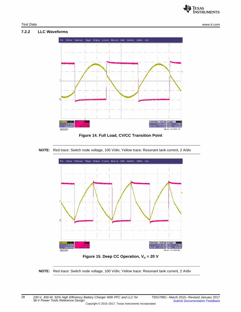
7.2.2 LLC Waveforms
Figure 14. Full Load, CV/CC Transition Point
NOTE: Red trace: Switch node voltage, 100 V/div; Yellow trace: Resonant tank current, 2 A/div
Figure 15. Deep CC Operation, VO = 20 V
NOTE: Red trace: Switch node voltage, 100 V/div; Yellow trace: Resonant tank current, 2 A/div

www.ti.com Test Data
29TIDU789C–March 2015–Revised January 2017Submit Documentation Feedback
Copyright © 2015–2017, Texas Instruments Incorporated
230-V, 400-W, 92% High Efficiency Battery Charger With PFC and LLC for36-V Power Tools Reference Design
7.2.3 Output Diode Stress
Figure 16. Full Load, CV/CC Transition Point
NOTE: Red trace: Output diode reverse voltage, 20 V/div
Figure 17. Deep CC Operation, VO = 20 V
NOTE: Red trace: Output diode reverse voltage, 10 V/div

Test Data www.ti.com
30 TIDU789C–March 2015–Revised January 2017Submit Documentation Feedback
Copyright © 2015–2017, Texas Instruments Incorporated
230-V, 400-W, 92% High Efficiency Battery Charger With PFC and LLC for36-V Power Tools Reference Design
7.2.4 Bias Supply Switching Waveforms
Figure 18. Auxiliary Output (5 V) Loaded to 100 mA
NOTE: Red trace: Collector voltage, 100 V/div; Yellow trace: Collector current, 100 mA/div

www.ti.com Test Data
31TIDU789C–March 2015–Revised January 2017Submit Documentation Feedback
Copyright © 2015–2017, Texas Instruments Incorporated
230-V, 400-W, 92% High Efficiency Battery Charger With PFC and LLC for36-V Power Tools Reference Design
7.2.5 Output Ripple and Noise
Figure 19. Full Load, CV/CC Transition Point
NOTE: Red trace: Output voltage ripple and noise, 100 mV/div
Figure 20. CC Operation, VO = 40 V
NOTE: Red trace: Output voltage ripple and noise, 500 mV/div;Yellow trace: Output current ripple, 1 A/div

Test Data www.ti.com
32 TIDU789C–March 2015–Revised January 2017Submit Documentation Feedback
Copyright © 2015–2017, Texas Instruments Incorporated
230-V, 400-W, 92% High Efficiency Battery Charger With PFC and LLC for36-V Power Tools Reference Design
7.2.6 Start-Up
Figure 21. Deep CC Operation, VO = 20 V
NOTE: Red trace: Output voltage, 20 V/div; Yellow trace: Input current, 2 A/div
7.2.7 Inrush
Figure 22. VIN = 265-V AC, Full Load
NOTE: Yellow trace: Input current, 10 A/div

www.ti.com Test Data
33TIDU789C–March 2015–Revised January 2017Submit Documentation Feedback
Copyright © 2015–2017, Texas Instruments Incorporated
230-V, 400-W, 92% High Efficiency Battery Charger With PFC and LLC for36-V Power Tools Reference Design
7.3 Conducted Emissions
7.3.1 Emissions at Full LoadGenerally conducted emissions will be more at full load. So, this operating point is chosen for measuringconducted EMI.
230-V AC input, 42-V, 9-A simulated battery load connected to PSU output with short leads.
The conducted peak emissions in a pre-compliance test set-up were compared against EN55022 Class-Aquasi-peak limits and found to be meeting them comfortably so the quasi-peak emissions can also meetthem easily.
Figure 23. Conducted Peak Emissions at Full Load

Test Data www.ti.com
34 TIDU789C–March 2015–Revised January 2017Submit Documentation Feedback
Copyright © 2015–2017, Texas Instruments Incorporated
230-V, 400-W, 92% High Efficiency Battery Charger With PFC and LLC for36-V Power Tools Reference Design
230-V AC input, 42-V, 9-A simulated battery load connected to PSU output with short leads.
The conducted average emissions in a pre-compliance test setup were compared against EN55022 Class-A average limits and found to be meeting them.
Figure 24. Conducted Average Emissions at Full Load

www.ti.com Test Data
35TIDU789C–March 2015–Revised January 2017Submit Documentation Feedback
Copyright © 2015–2017, Texas Instruments Incorporated
230-V, 400-W, 92% High Efficiency Battery Charger With PFC and LLC for36-V Power Tools Reference Design
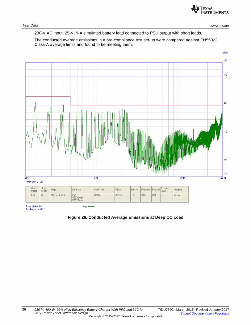
7.3.2 Emissions at Deep CC LoadGenerally conducted emissions will be more at full load. However, the LLC-stage operating frequency is atits maximum in deep CC operating point. So this operating point is also chosen for measuring conductedEMI to verify if the increased operating frequency causes increased EMI.
230-V AC input, 25-V, 9-A simulated battery load connected to PSU output with short leads.
The conducted peak emissions in a pre-compliance test set-up were compared against EN55022 Class-Aquasi-peak limits and found to be meeting them comfortably. So the quasi-peak emissions can also meetthem easily.
Figure 25. Conducted Peak Emissions at Deep CC Load
Test Data www.ti.com
36 TIDU789C–March 2015–Revised January 2017Submit Documentation Feedback
Copyright © 2015–2017, Texas Instruments Incorporated
230-V, 400-W, 92% High Efficiency Battery Charger With PFC and LLC for36-V Power Tools Reference Design
230-V AC input, 25-V, 9-A simulated battery load connected to PSU output with short leads.
The conducted average emissions in a pre-compliance test set-up were compared against EN55022Class-A average limits and found to be meeting them.
Figure 26. Conducted Average Emissions at Deep CC Load

www.ti.com Design Files
37TIDU789C–March 2015–Revised January 2017Submit Documentation Feedback
Copyright © 2015–2017, Texas Instruments Incorporated
230-V, 400-W, 92% High Efficiency Battery Charger With PFC and LLC for36-V Power Tools Reference Design
8 Design Files
8.1 SchematicsTo download the most recent schematics, see the design files at TIDA-00355.
8.2 Bill of MaterialsTo download the most recent bill of materials (BOM), see the design files at TIDA-00355.
8.3 PCB Layout RecommendationsA careful PCB layout is critical for proper operation of power electronics devices. As with all switchingpower supplies, attention to detail in the layout can save much time in troubleshooting later on.
8.3.1 Power Stage Specific GuidelinesKey guidelines for routing power stage components:• Minimize the loop area and trace length of the power path circuits, which contain high frequency
switching currents, on both the primary and secondary sides of the converter. This will help reduce EMIand improve converter overall performance.
• Keep traces with high dV/dt potential and high di/dt capability away from or shielded from sensitivesignal traces.
• Keep power ground and control ground separately for each power supply stage. If they areelectronically connected, tie them together in one point near DC input return or output return of thegiven stage correspondingly.
• When multiple capacitors are used in parallel for current sharing, layout should be symmetrical acrossboth leads of the capacitors. If the layout is not identical, the capacitor with the lower series traceimpedance will see higher peak currents and become hotter (i2R).
• Tie the heat-sinks of all the power switching components to their respective power grounds.• Place protection devices such as TVS, snubbers, capacitors, or diodes physically close to the device
they are intended to protect, and routed with short traces to reduce inductance.• Choose the width of PCB traces based on acceptable temperature rise at the rated current per
IPC2152 as well as acceptable DC and AC impedances. Also, the traces should withstand the faultcurrents (such as short circuit current) before the activation of electronic protection such as fuse orcircuit breaker.
• Determine the distances between various circuits according to the requirements of applicablestandards, such as UL60950.
• Adapt thermal management to fit the end-equipment requirements.
8.3.2 Controller Specific GuidelinesKey guidelines for routing of controller components and signal circuits:• The optimum placement of decoupling capacitor is closest to the VCC and GND terminals of the
device. Care must be taken to minimize the loop area formed by the bypass-capacitor connection andthe GND terminal of the IC.
• The reference ground for the device, a low current signal ground (SGND), should be a copper plane orisland.
• Locate all controller support components at specific signal pins (VSENSE, VCOMP, ISENSE, ICOMP,FREQ) close to their connection pin. Connect the other end of the component to the SGND withshortest trace length.
• The trace routing for the voltage sensing and current sensing circuit components to the device shouldbe as short as possible to reduce parasitic effects on the current limit and current/voltage monitoringaccuracy. These traces should not have any coupling to switching signals on the board.
• The SGND plane must be connected to high current ground (main power ground) at a single point thatis at the negative terminal of DC input or output capacitor respectively.

Design Files www.ti.com
38 TIDU789C–March 2015–Revised January 2017Submit Documentation Feedback
Copyright © 2015–2017, Texas Instruments Incorporated
230-V, 400-W, 92% High Efficiency Battery Charger With PFC and LLC for36-V Power Tools Reference Design
8.3.3 Layer PlotsTo download the most recent layer plots, see the design files at TIDA-00355.
8.4 Altium ProjectTo download the most recent Altium project files, see the design files at TIDA-00355.
8.5 Gerber FilesTo download the most recent Gerber files, see the design files at TIDA-00355.
8.6 Assembly DrawingsTo download the most recent assembly drawings, see the design files at TIDA-00355.
9 References
1. Texas Instruments, Designing an LLC Resonant Half-Bridge Power Converter, Power Supply DesignSeminar: SEM1900, Topic 3 (SLUP263)
2. Texas Instruments, Feedback Loop Design of an LLC Resonant Power Converter, Application Report(SLUA582)
3. Texas Instruments, A Design Review of a Full-Featured 350-W Offline Power Converter, SEM2000,Topic 2, (TIDU186)
4. Texas Instruments, Exposing the Inner Behavior of a Quasi-Resonant Flyback Converter, SEM2000,Topic 3 (SLUP302)
5. Texas Instrument, Snubber Circuits: Theory, Design and Applications (SLUP100)6. Texas Instruments, UCC28722/UCC28720 5W USB BJT Flyback Design Example, Application Report
(SLUA700)7. S. Y. R. Hui and H. Chung, Resonant and Soft-Switching Converters, In: M. H. Rashid, Ed., Power
Electronics Handbook, Academic Press, Cambridge, 2000, pp. 271 – 304.
9.1 Trademarks
10 About the AuthorSALIL CHELLAPPAN is a lead engineer, member, and group technical staff at Texas Instruments, wherehe is responsible for developing customized power solutions as part of the Power Design Services group.Salil brings to this role his extensive experience in power electronics, power conversion, EMI/EMC, powerand signal integrity, and analog circuits design spanning many high-profile organizations. Salil holds abachelor of technology degree from the University of Kerala.
LATIF AMEER BABU is a systems engineer at Texas Instruments, where he is responsible for developingreference design solutions for the industrial segment. Latif brings to this role his extensive experience inpower electronics, high-frequency DC-DC converter, and analog circuit design. Latif earned his master oftechnology in power electronics and power systems from Indian Institute of Technology, Mumbai; IN. Latifis a member of the Institute of Electrical and Electronics Engineers (IEEE).

www.ti.com Revision History A and B
39TIDU789C–March 2015–Revised January 2017Submit Documentation Feedback
Copyright © 2015–2017, Texas Instruments Incorporated
Revision History
Revision History A and BNOTE: Page numbers for previous revisions may differ from page numbers in the current version.
Changes from Original (March 2015) to B Revision ....................................................................................................... Page
• Changed title from 230-V, 400-W High Efficiency Battery Charger With PFC and LLC for 36-V Power Tools to 230-V, 400-W, 92% High Efficiency Battery Charger With PFC and LLC for 36-V Power Tools Reference Design ...................... 1

Revision History C www.ti.com
40 TIDU789C–March 2015–Revised January 2017Submit Documentation Feedback
Copyright © 2015–2017, Texas Instruments Incorporated
Revision History
Revision History C
Changes from B Revision (May 2016) to C Revision ...................................................................................................... Page
• Deleted schematic images from document; updated images available in the TIDA-00355 tool folder on TI.com .......... 37• Deleted BOM from document; up-to-date BOM available in the TIDA-00355 tool folder on TI.com ......................... 37• Deleted layer plot images from document; images available in the TIDA-00355 tool folder on TI.com...................... 38• Deleted Altium project image from document; image available in the TIDA-00355 tool folder on TI.com ................... 38• Deleted Gerber file image from document; image available in the TIDA-00355 tool folder on TI.com....................... 38• Deleted assembly drawing images from document; images available in the TIDA-00355 tool folder on TI.com ........... 38

IMPORTANT NOTICE FOR TI DESIGN INFORMATION AND RESOURCES
Texas Instruments Incorporated (‘TI”) technical, application or other design advice, services or information, including, but not limited to,reference designs and materials relating to evaluation modules, (collectively, “TI Resources”) are intended to assist designers who aredeveloping applications that incorporate TI products; by downloading, accessing or using any particular TI Resource in any way, you(individually or, if you are acting on behalf of a company, your company) agree to use it solely for this purpose and subject to the terms ofthis Notice.TI’s provision of TI Resources does not expand or otherwise alter TI’s applicable published warranties or warranty disclaimers for TIproducts, and no additional obligations or liabilities arise from TI providing such TI Resources. TI reserves the right to make corrections,enhancements, improvements and other changes to its TI Resources.You understand and agree that you remain responsible for using your independent analysis, evaluation and judgment in designing yourapplications and that you have full and exclusive responsibility to assure the safety of your applications and compliance of your applications(and of all TI products used in or for your applications) with all applicable regulations, laws and other applicable requirements. Yourepresent that, with respect to your applications, you have all the necessary expertise to create and implement safeguards that (1)anticipate dangerous consequences of failures, (2) monitor failures and their consequences, and (3) lessen the likelihood of failures thatmight cause harm and take appropriate actions. You agree that prior to using or distributing any applications that include TI products, youwill thoroughly test such applications and the functionality of such TI products as used in such applications. TI has not conducted anytesting other than that specifically described in the published documentation for a particular TI Resource.You are authorized to use, copy and modify any individual TI Resource only in connection with the development of applications that includethe TI product(s) identified in such TI Resource. NO OTHER LICENSE, EXPRESS OR IMPLIED, BY ESTOPPEL OR OTHERWISE TOANY OTHER TI INTELLECTUAL PROPERTY RIGHT, AND NO LICENSE TO ANY TECHNOLOGY OR INTELLECTUAL PROPERTYRIGHT OF TI OR ANY THIRD PARTY IS GRANTED HEREIN, including but not limited to any patent right, copyright, mask work right, orother intellectual property right relating to any combination, machine, or process in which TI products or services are used. Informationregarding or referencing third-party products or services does not constitute a license to use such products or services, or a warranty orendorsement thereof. Use of TI Resources may require a license from a third party under the patents or other intellectual property of thethird party, or a license from TI under the patents or other intellectual property of TI.TI RESOURCES ARE PROVIDED “AS IS” AND WITH ALL FAULTS. TI DISCLAIMS ALL OTHER WARRANTIES ORREPRESENTATIONS, EXPRESS OR IMPLIED, REGARDING TI RESOURCES OR USE THEREOF, INCLUDING BUT NOT LIMITED TOACCURACY OR COMPLETENESS, TITLE, ANY EPIDEMIC FAILURE WARRANTY AND ANY IMPLIED WARRANTIES OFMERCHANTABILITY, FITNESS FOR A PARTICULAR PURPOSE, AND NON-INFRINGEMENT OF ANY THIRD PARTY INTELLECTUALPROPERTY RIGHTS.TI SHALL NOT BE LIABLE FOR AND SHALL NOT DEFEND OR INDEMNIFY YOU AGAINST ANY CLAIM, INCLUDING BUT NOTLIMITED TO ANY INFRINGEMENT CLAIM THAT RELATES TO OR IS BASED ON ANY COMBINATION OF PRODUCTS EVEN IFDESCRIBED IN TI RESOURCES OR OTHERWISE. IN NO EVENT SHALL TI BE LIABLE FOR ANY ACTUAL, DIRECT, SPECIAL,COLLATERAL, INDIRECT, PUNITIVE, INCIDENTAL, CONSEQUENTIAL OR EXEMPLARY DAMAGES IN CONNECTION WITH ORARISING OUT OF TI RESOURCES OR USE THEREOF, AND REGARDLESS OF WHETHER TI HAS BEEN ADVISED OF THEPOSSIBILITY OF SUCH DAMAGES.You agree to fully indemnify TI and its representatives against any damages, costs, losses, and/or liabilities arising out of your non-compliance with the terms and provisions of this Notice.This Notice applies to TI Resources. Additional terms apply to the use and purchase of certain types of materials, TI products and services.These include; without limitation, TI’s standard terms for semiconductor products http://www.ti.com/sc/docs/stdterms.htm), evaluationmodules, and samples (http://www.ti.com/sc/docs/sampterms.htm).
Mailing Address: Texas Instruments, Post Office Box 655303, Dallas, Texas 75265Copyright © 2017, Texas Instruments Incorporated