Embed Size (px)
Citation preview
21.3
Leakage-Aware Intraprogram Voltage Scaling forEmbedded Processors
Po-Kuan Huang Soheil GhiasiDepartment of Electrical and Computer Department of Electrical and Computer
Engineering EngineeringUniversity of California, Davis University of California, Davis
Davis, CA Davis, [email protected] [email protected]
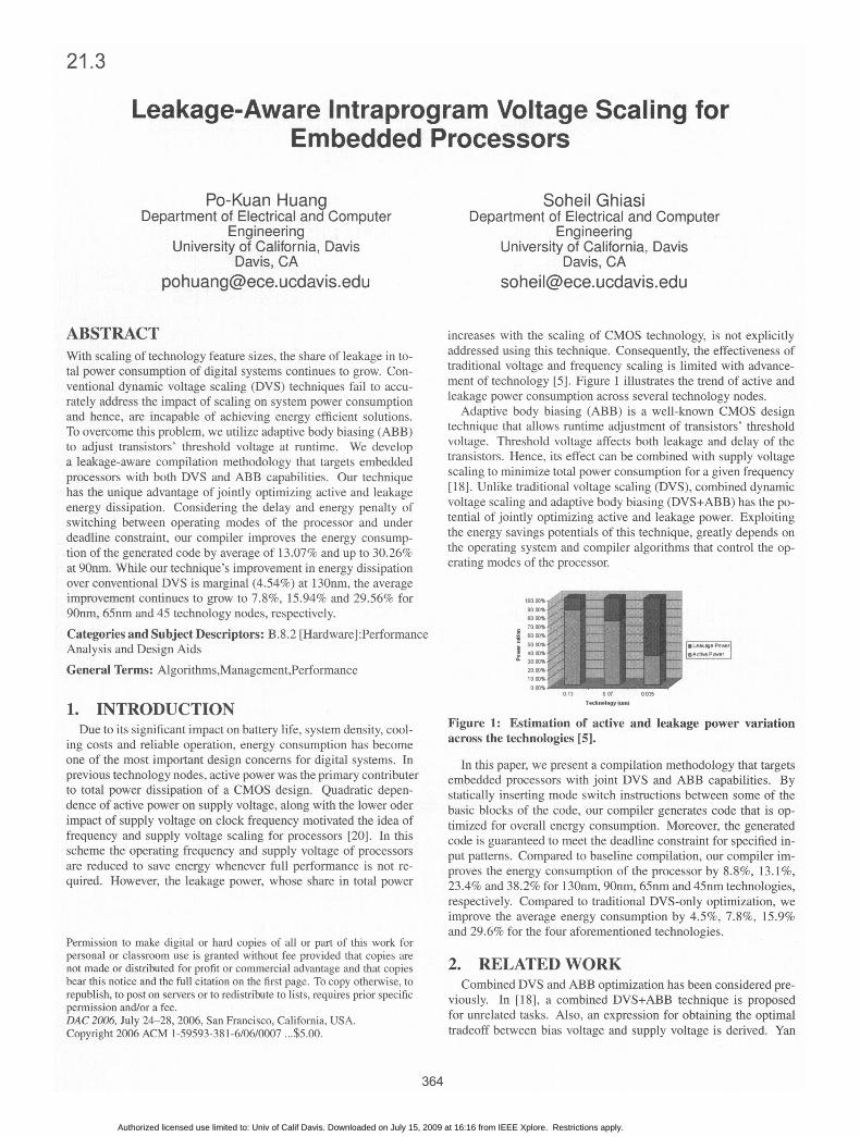
ABSTRACT increases with the scaling of CMOS technology, is not explicitlyWith scaling of technology feature sizes, the share of leakage in to- addressed using this technique. Consequently, the effectiveness oftal power consumption of digital systems continues to grow. Con- traditional voltage and frequency scaling is limited with advance-ventional dynamic voltage scaling (DVS) techniques fail to accu- ment of technology [5]. Figure 1 illustrates the trend of active andrately address the impact of scaling on system power consumption leakage power consumption across several technology nodes.and hence, are incapable of achieving energy efficient solutions. Adaptive body biasing (ABB) is a well-known CMOS designTo overcome this problem, we utilize adaptive body biasing (ABB) technique that allows runtime adjustment of transistors' thresholdto adjust transistors' threshold voltage at runtime. We develop voltage. Threshold voltage affects both leakage and delay of thea leakage-aware compilation methodology that targets embedded transistors. Hence, its effect can be combined with supply voltageprocessors with both DVS and ABB capabilities. Our technique scaling to minimize total power consumption for a given frequencyhas the unique advantage of jointly optimizing active and leakage [18]. Unlike traditional voltage scaling (DVS), combined dynamicenergy dissipation. Considering the delay and energy penalty of voltage scaling and adaptive body biasing (DVS+ABB) has the po-switching between operating modes of the processor and under tential of jointly optimizing active and leakage power. Exploitingdeadline constraint, our compiler improves the energy consump- the energy savings potentials of this technique, greatly depends ontion of the generated code by average of 13.07% and up to 30.26% the operating system and compiler algorithms that control the op-at 90nm. While our technique's improvement in energy dissipation erating modes of the processor.over conventional DVS is marginal (4.54%) at 130nm, the averageimprovement continues to grow to 7.8%, 15.94% and 29.56% for l0a 0*90nm, 65nm and 45 technology nodes, respectively.Categories and Subject Descriptors: B.8.2 [Hardware]:Performance 7 OAnalysis and Design Aids I
30 MS
General Terms: Algorithms,Management,Performance 20O0S
013 007 00351. INTRODUCTION lZffP3Due to its significant impact on battery life, system density, cool- Figure 1: Estimation of active and leakage power variation
ing costs and reliable operation, energy consumption has become across the technologies [5].one of the most important design concerns for digital systems. In In this paper, we present a compilation methodology that targetsprevious technology nodes, active power was the primary contributer embedded processors with joint DVS and ABB capabilities. Byto total power dissipation of a CMOS design. Quadratic depen- statically inserting mode switch instructions between some of thedence of active power on supply voltage, along with the lower oder basic blocks of the code, our compiler generates code that is op-impact of supply voltage on clock frequency motivated the idea of timized for overall energy consumption. Moreover, the generatedfrequency and supply voltage scaling for processors [20]. In this code is guaranteed to meet the deadline constraint for specified in-scheme the operating frequency and supply voltage of processors put patterns. Compared to baseline compilation, our compiler im-are reduced to save energy whenever full performance is not re- proves the energy consumption of the processor by 8.8%, 13.1%,quired. However, the leakage power, whose share in total power 23.4% and 38.2% for 130nm, 90nm, 65nm and 45nm technologies,
respectively. Compared to traditional DVS-only optimization, weimprove the average energy consumption by 4.5%, 7.8%, 15.9%and 29.6% for the four aforementioned technologies.
Permission to make digital or hard copies of all or part of this work forpersonal or classroom use is granted without fee provided that copies arenot made or distributed for profit or commercial advantage and that copies 2. RELATEDWORKbear this notice and the full citation on the first page. To copy otherwise, to Combined DVS and ABB optimization has been considered pre-republish, to post on servers or to redistribute to lists, requires prior specific viously. In [18], a combined DVS+ABB technique is proposedpermission and/or a fee.DAC 2006, July 24-28, 2006, San Francisco, California, USA. for unrelated tasks. Also, an expression for obtaining the optimalCopyright 2006 ACM 1-59593-381-6/06/0007 $5.00. tradeoff between bias voltage and supply voltage is derived. Yan
364
Authorized licensed use limited to: Univ of Calif Davis. Downloaded on July 15, 2009 at 16:16 from IEEE Xplore. Restrictions apply.
et al. proposed an algorithm for a task graph with real-time con- 3.2 Threshold Voltagestraints [9]. None of the previous work on combined DVS+ABB The threshold voltage of a short-channel MOSFET transistor ishave considered intra-task level optimization, which requires pro- given by [16]:gram structure analysis.
Several research efforts have proposed static intraprogram volt-age scaling [6, 15, 3, 4]. An analytical study of potential power sav- Vth = Vth, + Y( SO--Vb-V) + HDIBLVdd + AVNW (1)ings using intraprogram DVS is reported in [6]. The authors also where Vtho is the threshold voltage at zero bias voltage, y, Os,propose an ILP-based based approach whose savings come reason- where onstantshold vete zero bis the y bsably close to the analytical bounds. In [3], checkpoints indicating and bDeBLare constants for a given technology, Vbs is the body biasthe voltage scaling points are inserted to program during compila- voltage between the substrate and source of the transistor, AVNWistion. Hsu et al. introduce an algorithm that identifies the program a constant that models narrow width effects, and Vdd is the supplyregions with time slack for processor, and implement it as a source- voltage. If l 4bs the threshold voltage can be linearized:to-source transformation[4]. Compiler and operating system leveloptimization are coordinated in [ 15]. None of these techniques con- Vth = Vth,- K * Vdd - K2 Vb, (2)sider leakage power, and the effect of technology scaling on the va- where KI, K2, and Vth, are constants [18]. Equation 2 formal-lidity of their results. We utilize the generic power model derived in izes the impact of supply and body voltage scaling on the threshold[18], and perform intraprogram simultaneous DVS and ABB. Us- volthe.ing cycle-accurate simulators, we estimate the energy consumption voltage.of some embedded application to demonstrate the efficiency of our 3.3 Power Consumptionproposed method. The power consumption ofCMOS circuits includes active, leak-
age, and short circuit power. The short circuit power consumption3. POWER AND PERFORMANCEUNDER is much smaller than active and leakage power, and is negligible.
DVS AND ABB The dynamic power Pd is given by:
3.1 Background = CeffVdf (3)In this section, we briefly overview the impact of supply voltage where Ceff is the average switched capacitance per cycle, and
and body bias on processor's frequency and power consumption.We summarize the previous study by Martin et. al. [ 1 8] that derives approximated as:threshold voltage, power consumption, and the performance of thedesign as functions of its supply and bias voltages. Subsequently,we proceed to present the power and performance parameters of Ps - VddIs.b, + IVbsI (Iij + Ib) (4)the proposed processor with DVS and ABB capabilities. where Iu,b is the subthreshold leakage current, and Ij, and Ib,lDVS allows the microprocessor to scale its supply voltage and are the drain and source to body junction leakage currents in the
operating frequency at runtime. With semi-linear reduction in sup- NMOS device [12, 13, 17]. Considering the relation between sub-ply voltage and frequency, DVS obtains quadratic saving in dy- threshold leakage current, operating conditions (frequency, supplynamic energy. In practice, the processor has several distinct voltage- voltage, and body bias) and process technology, the overall powerfrequency modes. Modes with higher frequency are implemented consumption can be summarized as:with higher supply voltage, in which, the processor runs faster andconsumes more energy for executing a particular task.ABB is a simple-to-implement technique to control subthresh- P = CeffVgjdf+ VddK3ek4VddeK5Vb + Vb Ii (5)
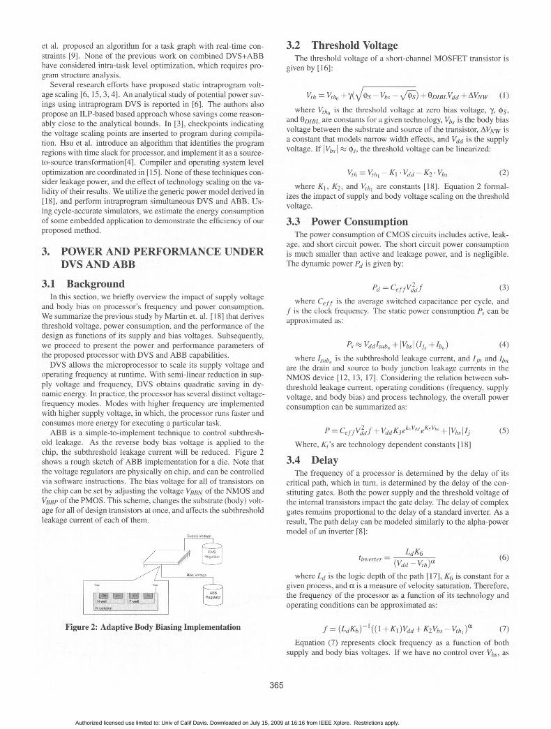
old leakage. As the reverse body bias voltage is applied to the Where, Ki's are technology dependent constants [18]chip, the subthreshold leakage current will be reduced. Figure 2shows a rough sketch of ABB implementation for a die. Note that 3.4 Delaythe voltage regulators are physically on chip, and can be controlled The frequency of a processor is determined by the delay of itsvia software instructions. The bias voltage for all of transistors on critical path, which in turn, is determined by the delay of the con-the chip can be set by adjusting the voltage VBBN of the NMOS and stituting gates. Both the power supply and the threshold voltage ofVBBP of the PMOS. This scheme, changes the substrate (body) volt- the internal transistors impact the gate delay. The delay of complexage for all of design transistors at once, and affects the subthreshold gates remains proportional to the delay of a standard inverter. As aleakage current of each of them. result, The path delay can be modeled similarly to the alpha-power
model of an inverter [8]:
/ 7 =u,ato tinverter LdK6
lV where Ld is the logic depth of the path [17], K6 is constant for agiven process, and a is a measure of velocity saturation. Therefore,
[t-I IPEWB0: ' 1 lRe,BB,, the frequency of the processor as a function of its technology andoperating conditions can be approximated as:
Figure 2: Adaptive Body Biasing Implementation f = (LdK6)1 ((I +K1)Vdd + K2Vb - Vth, )' (7)
Equation (7) represents clock frequency as a function of bothsupply and body bias voltages. If we have no control over Vbs, as
365
Authorized licensed use limited to: Univ of Calif Davis. Downloaded on July 15, 2009 at 16:16 from IEEE Xplore. Restrictions apply.

is the case with traditional voltage scaling, there is a unique sup- Operating frequency(MHz) 1000 800 600 400 200ply voltage that would force the processor to operate at a given Supply voltage(V) 1.63 1.47 1.029 1-.11 -0.57frequency. However, having DVS+ABB capability allows many ias voltage -0. - .potential settings of supply and body bias to force the processor tooperate at a given frequency. Martin et. al. proposed an equationthat can be used to find the energy optimal settings of supply andbody bias for a given clock frequency [ 18]. 5. LEAKAGE-AWARE COMPILATION
4 DVS+ABB ENABLED PROCESSORMODEL Our compiler optimization goal is to minimize the applicationDVS+argetaBBrocessor that ENABLEDlPROCESSOR MODueL- total energy consumption by assigning different basic blocks of theWe target a processor that can operate at several discrete frequen- code to different processor operating modes (or simply modes) sub-
cies. According to Section 3, each frequency is associated with ject to meeting the deadline of the application. We also consider thea corresponding pair of supply and body bias voltages that allow energy and latency penalty of switching modes. We aim to performoperation of the processor at that frequency. The combination of mode switching, by insertion of mode switch instructions on thethe three parameters, i.e., frequency, supply voltage and body bias, control flow edges of the application. Since there might be severalconstitute an operating mode of the processor. The processor is as- control flow edges that arrive at a common destination, differentsumed to be able to switch between operating modes by execution iterations of a basic block might be executed in different operatingof a specialized instruction, referred to as mode switch instruction. modes. However, subsequent iterations over a particular controlGiven an operating mode, a mode switch instruction can set both flow edge would always switch the processor to a specific mode. Athe supply voltage and body bias of the processors to switch to that similar approach has been used by Xie et al. [6] for DVS-enabledoperating mode. Note that the frequency is a function of supply and processor, however, their technique neglects the leakage contribu-body bias voltage, and does not need to be specified separately. tion to total power consumption. We formulate the problem to con-
Execution of the mode switch instruction, or equivalently switch- sider both dynamic voltage scaling and adaptive body biasing.ing between modes, incurs delay and energy penalty. Both delay Figure 3 shows a partial view of a program control flow structure,and energy penalty depend on the voltage difference of the two which illustrates sample branches, loops, and self-loops among themodes involved in switching. The deadline requirement and energy basic blocks. We analyze the structure of the application and profileoptimization will be handled by our compilation methodology, and the typical execution traces of the application to extract the requiredhence, the architecture does not have to utilize a power and dead- statistical information such as the average latency and the averageline monitoring mechanism. energy consumption for each basic block under a particular mode,
According to Equation 7, there are infinitely many (supply volt- and the frequency of traversing edges. We utilize the extracted in-age, body bias voltage) pairs that can cause the processor to operate formation to perform mode assignment to execution traces of theat a given frequency. We utilize the equations (8) and (9) derived in application, under deadline constraint. We proceed to formulate[18] to find the energy optimal supply and body bias voltages that this problem as an mixed-integer linear programming (MILP) in-result in a given frequency and process technology. Equation (8) stance, which can be solved by application of commercially avail-illustrates the relationship between the bias voltage and the deriva- able solvers. Once mode assignments for control flow edges of thetive of the energy consumption per cycle. Equation (9) formulates application are decided, appropriate mode switching instructionsthe supply voltage as the function of the bias voltage. are inserted to the code.
( LgK3f 1 ( K, Vbs + K2 ) eK3Vbs+K4 - IjLgf-1 M B
aE-yc + 2Ceff ( KSVbs + K6) if Vdd > 0.5 () A B
Lg ( K3K5eeKs5vbs + 0.5K4 - 2I ) otherwise
Vdd = ( LdK6f - K2Vbs + Vthl )/( +Ki ) (9)
Where ECYC is the energy consumption per cycle and Lg is the DO&
number of logic gates in the circuit. The selection of the operat-ing modes is an important issue for both performance and energyconsumption. The processors with too few operating modes can-not completely exploit the execution slack. On the other hand, too Upon switching the operating mode of the processor, the supplymany operating modes would introduce extra complexity for hard- and body bias voltage regulators have to charge the capacitance.ware designers with very little energy improvement. The charging of capacitance incurs some energy penalty, which canWe assume that our target processor can operate at 5 different be estimated as:
clock frequencies, from 200MHz up to IGHz at 200MHz steps.We adopt the process technology and processor parameters from 2 2 2 2Predictive Technology Models [1] and existing DVS-enabled com- Es = (VddjVdd2 )Cr+(V -VbS2 )Cs (10)mercial processors [2], respectively. Using Equations (8) and (9), where Cr is the capacitance of the power trail and Cs is the capac-we obtain the energy optimal supply and body bias voltages corre- itance of the substrate of the device. Vdd and Vbs denote the supplysponding to each frequency. Table 1 demonstrates the characteris- and body bias voltages, respectively [20].tics of the operating modes for our target processor in 9Onm. We associate a binary decision variable kbcm to represent the op-
erating mode on the edge (b, c) of the application CDFG. kbcm isset to 1 if and only if the operating mode on the edge (b, c) is setto mode m. We use the constant FErn to denote the average energy
366
Authorized licensed use limited to: Univ of Calif Davis. Downloaded on July 15, 2009 at 16:16 from IEEE Xplore. Restrictions apply.

consumption of the basic block c in mode m. Constant Dabc is usedto represent the number of times basic block b is entered through Nedge (a, b) and exited through edge (b, c) (Figure 3). Dabc repre- kbm= 1 (14)sents the transition into and out of basic block b, which assists us m=1in determining whether the two edges will incur a mode switch, or The absolute and max function used in equations ( 1) and (13) isthey will run in the same operating mode. The value of Dabc can not an MILP problem. To linearize the max function in the equationbe determined or estimated by application profiling. Similarly, Gbc (13), we define a new variable which is greater than both elementsdenotes the number of executions of edge (b, c). therefore, the total inside the max function. We introduce variable eabc to linearizeenergy consumption of the application is given by: the terms corresponding to supply voltage in equations (11). Three
other variables and corresponding constraints are also added, to lin-R R N R R R N earize the terms associated with supply voltage in (13), and with
2 GbckbcmEcm+ abDa E (kabmVMs -kbcmVm,s) Cr body bias voltage in (11) and (13). The corresponding constraintsb=_ c=l m=1 a=l b=1 c=1m=1 are removed for brevity.
R R R N N
+x ,Dabc E(kabmVr,b kbcmV,b) Cs (11) -eabc.<V(kbbmVS ckbmV,s) < eabc (15)a=lb=lc=1 m=1 m= 1
Where Vm,s and Vm,b are constants representing the supply and 6 EXPERIMENTAL RESULTSbias voltage under operating mode m. R is the number of the ba- 6sic blocks in the control-flow graph, and N is the number of the 6.1 Experimental Setupoperating modes of the microprocessor. The first term of Equation( 11) represents the energy consumption for execution of the basic In order to verify the effectiveness of our intraprogram combinedblocks at their associated operating modes. The second and third voltage scaling and body biasing technique, we have developed aterms are the switching energy penalty caused by DVS and ABB, compilation flow to generate executable code for our target proces-respectively. Hence, the objective of our optimization is to mini- sor. Figure 4 illustrates our experimental setup. We have instru-mize Equation ( 11) by manipulating the operating variables kbcm. mented widely used compiler infrastructure, cycle-accurate perfor-The latency of the application is the sum total of the execution mance and energy simulators to obtain the required profiling infor-
latency of basic blocks in all iterations and the delay penalty associ- mation for each benchmark application. Subsequently, we generateated with mode switches. The switching delay can be approximated the MILP problem and invoke a commercial solver to obtain theas the time required to charge the capacitance by voltage regulators optimized operating mode for each control flow edge of the CDFG.[20]: The MILP solution is read by our compiler, which inserts corre-
sponding mode switch instructions on control flow edges before2Cr 2Cs code generation. Finally, the generated code is simulated using
Es = (Vdd - Vdd2) 21 + (Vbsi -Vbs2)2I (12) cycle-accurate simulators to measure its energy consumption, andYr,max Ns,max to ensure that it meets the deadline constraint.where Irmax and Is,max are the maximum possible currents. The
execution deadline constraint of the application can be written as C Codethe following inequality:
[SUIFCompiler | Power PertormanceSUFCm Ier Simulator Siuao
R GK Ck~1~TCm+ NIjI7~ Application Protiling and MILP Generation
L ,2,GbckbcmTcm+ MILP.. .1 m=1 ~~~~~~~~~~~~~~~~~~~~~~~~~~~~~~CompilerOptimizatin+b=l c=l m=l solver Cod Goertbnms
R R R N DVS+ABB Simulator
Max E 1£ I Dabc E (kabmVm,s - kbcmVm,s) CRa=1 b= c=1 m=1 Execution time and energy dissipation
Figure 4: The setup of experiments for leakage-aware compila-R RR N ]tionEE5E Dabc E (kabmVm,b- kbcmVm,b) CB < deadlinea=lb=lc=l m=1 The first stage of our compilation methodology is to profile a
(13) given application to obtain the required information for our pro-where CR and CB are constants equal to 2Cr and I 5, respec- posed MILP formulation. The required information include aver-tively. Tcm is the average latency of basic block c under mode m, age delay and energy dissipation of program basic blocks in eachand Vmns and Vm,b are constants representing the supply and body operating mode (Ecm and Tcm in Equations 11 and 13), and exe-bias voltages in mode m. The optimization object of MILP formu- cution frequency of control flow edges with respect to precedinglation is to minimize (11), which quantifies the energy consump- active basic block (Gbc and Dabc in Equation 11). The front endtion of the compiled application. For most of embedded applica- of our compiler is based on the MachineSUIF compiler frameworktions, the compiled code has to guarantee an execution deadline. [14, 11]. We utilized MachineSUIF to generate CDFG representa-We model this constraint by (13), which would prevent the MILP tion of a program, and extract profiling information that relate tosolver to generate solutions that violate the deadline constraint. An- execution frequency of basic blocks.other MILP constraint is that the summation of the mode variables Furthermore, we need to know the average latency and energyon each edge should be exactly 1 to guarantee a unique assignment dissipation of basic blocks under each operating frequency. Noteof each edge to an operating mode: that the memory is not synchronous with processor, and has a rather
367
Authorized licensed use limited to: Univ of Calif Davis. Downloaded on July 15, 2009 at 16:16 from IEEE Xplore. Restrictions apply.

constant access time. Therefore, frequency scaling leads to a dif- could be substantial. Furthermore, insertion of new basic blocksferent set of cache misses/hits, and hence, different number of cy- changes the CFG structure of the program. Careless insertion ofcles to execute the program. We have modified the simplescalar basic block introduces redundant jump/branch instructions that cansimulator [19] to report the average latency of each basic block. be optimized using standard compiler optimization techniques. WeA modified XTREM simulator [7] is used to report average en- apply standard optimization techniques to remove redundant modeergy dissipation of basic blocks. This methodology gives us cycle- switches, and improve the performance and energy dissipation ofaccurate estimation of basic block latency and energy dissipation. the generated code.Once the necessary profiling information are gathered, we gener-ated the MILP instance. The CPLEX package is used to solve the (l 7lr7problem instances. "-Ie!U1We have selected five applications from MiBench[10] embedded Q
application suite as our testbenches. The selected applications rep- _ \resent several application domains of embedded systems, including > Inetworking, automotive, telecom and security. Table 2 reports the Mt 2 (R() MdeUdcharacteristics of the selected applications. The selected applica-tion domains justify the need for deadline constraint and realtime Figure 6: Examples of the redundant operating mode assign-operation of the generated code. ments
Benchmark Application # basic # lines Dynamicinstr. We have modified XTREM [7], a power simulator for Intel XS-domain blocks of code count (billion) cale DVS-enabled core, to estimate the energy dissipation of the
susan(comers) networkm 2038 343 238. generated code on the processor with DVS+ABB capabilities. Our
dijkstra network 36 174 14.11 simulator recognizes mode switch instructions and tracks the exe-adpcm(coder) telecom 33 281 9.35 cution time, leakage power and active power under frequency scal-
sha security 32 242 9.02 ing. For each frequency mode, two pairs of supply and body bias
Table 2: Selected testbenches and their characteristic voltages are used. For a given frequency, the DVS-enabled proces-sor has zero body bias, and hence, its supply voltage is differentfrom the DVS+ABB enabled processor. The optimal supply and
In order to investigate the effect of deadline relaxation on the bias voltage for each frequency are obtained using Equations (8)quality of different frequency scaling methods, we have carried out and (9). The developed simulator also considers the energy andour experiments using five different deadlines for each application. delay penalty of switching between modes.Figure 5 visualizes the relative location of deadlines in compari-son to baseline implementations. For each benchmark application, 6.2 Experimental Resultwe executed the program at all different frequency modes of the We implemented the experimental flow depicted in Figure 4 andprocessor (with no DVS or ABB mechanism) to obtain the base- generated code for five applications listed in Table 2. To examineline execution time of the application at each frequency. The first the impact of execution deadline and technology scaling, each ap-four deadlines are determined by averaging the adjacent execution plication testbench is experimented under twenty different settings,times. For example, the first deadline is equal to the average exe- i.e., five different execution execution deadlines (Figure 5) and fourcution time at IGHz and 800MHz frequencies, with no frequency different process technologies. The models and parameters of thescaling mechanism. The last (fifth) deadline is set to 95% of the process technology are obtained from [1]. The reported executionexecution time at the slowest mode, i.e., running the processor at time and energy dissipation are the numbers estimate from the gen-200MHz. erated code, using cycle-accurate simulators.
exec. time exec. time exec. time exec. time exec. time@1GHz @800MHz @60MHz @400MHz @200MHz
35.00
~3000Deadlinel Deadline2 Deadline3 Deadline4 DeadlineS 25 ._
Figure 5: Relation of deadlines to baseline execution times 1 s10
After solving the MILP problem instance, the appropriate execu- 500 45ntion mode for running each control flow edge is known. The second 02° 9.onologstage of the experiment is to insert mode switch instructions to con- D2 30- T.chWgytrol flow edges of the application. Our compiler inserts new basicblocks containing the appropriate mode switch instructions to con- Figure 7: Average improvements in energy savings: DVS+ABBtrol flow edges of the CFGs. However, it is possible that two con- compared to baseline executionsecutive mode switch instructions select the same operating mode,and hence, the second instruction redundant. Figure 6 shows exam- Table 3 presents the baseline execution time of the applications.ples of the redundant operating mode assignment. In the examples, These execution times are simulated for the processor running at abasic block C will always be executed under the operating mode particular operating frequency without the frequency scaling mech-of basic block B. Therefore we can remove the mode switch basic anism. For example, execution time at 800MHz would be the mostblock on the edge between basic block B and C. The mode switch energy efficient setting of the processor to meet deadline 2, with nobasic block on the edge from E to D is also considered redundant. frequency scaling. The table also reports the average (over twentyWe found that the negative impact of redundant mode switch in- different settings) MILP solution time for each application in sec-structions due to introduction of extra delay and energy penalty, onds.
368
Authorized licensed use limited to: Univ of Calif Davis. Downloaded on July 15, 2009 at 16:16 from IEEE Xplore. Restrictions apply.

Benchmark Exec. time Exec. time Exec. time Exec. time Exec. time Average MILP@IGHz @800MHz @600MHz @400MHz @200MHz solution time
adpcm 12.45 17.27 22.31 33.46 62.77 5.10sha 11.57 14.08 20.42 28.72 58.89 5.59
dijkstra 17.4 21.17 32.54 42.3 84.63 5.22susan 23.45 31.36 43.14 62.47 121.45 1588
patricia 28.43 38.01 52.14 74.61 146.21 183
Table 3: Applications execution time and MILP solution time (sec)
Due to the page limitation, we use two figures to show the en- processor. Experimental results advocating the effectiveness of ourergy impact of our method. Figure 7 illustrates the three dimen- approach, show that the energy dissipation gap between leakage-sional space of average energy savings over benchmark applica- aware and conventional DVS grows with technology scaling. Fu-tions, deadline, and process technology. The chart illustrates the ture works include coordination of dynamic and static leakage-DVS+ABB improvement in energy dissipation over baseline exe- aware voltage scaling techniques.cution of the code. In baseline execution, processor is constantlyrun at the minimum frequency that meets the deadline. Similarly, "REFERENCESFigure 8 compares the energy dissipation of DVS+ABB with con- IT] httpllxwww dintce.eecsl , eley edu/ ptm/introduction.html.
12] http://wwwisntel.com/design/intelxscale.ventional DVS, over various deadline and process technologies. [3] A. Azevedo, I. Issenin, R. Comea, R. Gupta, N. Dutt, A. Veidenbaum."Profile-Based Dynamic Voltage Scheduling Using Program Checkpoints". In
35 00 _ Design Automation and Test in Europe, pages 168-175, March 2002.[4] C.-H. Hsu, U. Kremer. "The Design, Implementation, and Evaluation of a
30.00 Compiler Algorithm for CPU Energy Reduction". In Conference on25.00 Programming Language Design and Implementation, pages 38-48, June 2003.2000 _ /.: 7 _ [5] D. Duarte, N. Vijaykrishnan, M. J. Irwin, H.-S. Kim, G. McFarland. "Impact of20.00
scaling on the effectiveness of dynamic power reduction schemes". In15.00 _5 /Proceeding of International Conference on Computer Design, pages 382-387,10.00 September 2002.5.00 45 [6] F Xie,M. Martonosi,S. Malik. "Intraprogram Dynamic Voltageo oo ssnn, Scaling:Bounding Opportunities with Analytic Modeling". ACM Transactions
D1n,, Teehoolory on Architecture and Code Optimization, 1(3):1-45, September 2004.03 D4 130nm [7] G. Contreras, M. Martonosi, J. Peng, R. Ju, G.Y. Lueh. "XTREM: a power
simulator for the Intel XScale core". ACM SIGPlAN Notices, 39(7):115-125,Figure 8: Average improvements in energy savings: DVS+ABB July 2004.
[8] K.A. Bowman, B.L. Austin, J.C. Eble, X. Tang, J.D. Meindl. "A physicalcompared to conventional DVS alpha-power law MOSFET model". IEEE Journal ofSolid-State Circuits,34(10):1410-1414, October 1999.
As figures 7 and 8 suggest, the energy savings significantly in- [9] L. Yan, J. Luo, N.K. Jha. "Combined dynamic voltage scaling and adaptivecrease with the relaxation of deadline, for a given process tech- body biasing for heterogeneous distributed real-time embedded systems". Innology. Intuitively, deadline relaxation increases the timing slack, IEEE/ACM International Conference on Computer-Aided Design, pages 30-37,
whichis beter eploitd by requecy scling ethod. Forexam-November 2003.which is better exploited by frequency scaling methods. For exam- [10] M. Guthaus, J. Ringenberg, D. Emst, T. Austin, and T. Mudge. "Mibench: aple in 65nm process, gradual relaxation of the timing constraint free, commercially representative embedded benchmark suite". In Proceedingfrom deadline I to deadline 5 leads to 2.94%, 8.52%, 16.48%, of the IEEE 4th Annual Workshop on Workload Characterization, pages 3-14,23.36% and 27.45% improvement in energy dissipation over base- December 2001.line6%executin.4 improvement in energydissipationoverbase-
[11] M.D. Smith, and G. Holloway. "An introduction to machine SUIF and itsline execution. portable libraries for analysis and optimization". Technical report, Division ofOn the other hand, DVS+ABB is aware of the leakage's contri- Engineering and Applied Sciences, Harvard University, 2002.
bution to total dissipated energy for each technology node. Thus, [12] M.J. Chen, H.T. Huang, C.S. Hou, K.N. Yang. "Back-gate bias enhancedit selects the operating modes such that the overall energy dissi- band-to-band tunneling leakage in scaled MOSFETS". IEEE Electron DeviceLetters, 19(4): 134-136, April 1998.pation, including leakage, is optimized. Consequently, DVS+ABB [13] M.R. Stan. "Optimal Voltages and Sizing for Low Power". In Intl. VLSI Designconsistently outperforms conventional DVS. It is interesting to note Conf, page 428, 1999.that DVS+ABB performs only slightly better than DVS for 130nm, [14] M.W. Hall, J.M. Anderson, S.P. Amarasinghe, B.R. Murphy, L. Shih-Wei, E.where, leakage energy is negligible. However with the shrinkage Bugnion, and MS. Lam. "Maximizing Multiprocessor Performance with theSUIF Compiler". Computer, 29(12):84-89, 1996.of the device sizes, the leakage energy increases exponentially. As [15] N. AbouGhazaleh, D. Mosse, B.R. Childers, R. G. Melhem, M. Craven.a result, the energy dissipation gap between the two methods grows "Collaborative Operating System and Compiler Power Management forwith technology scaling. For example considering deadline 4, our Real-Time Applications". In IEEE Real Time Technology and Applicationsapproach achieves 4.5%, 7.8%, 15.9% and 29.6% energy improve- Symposium, pages 133-143, 2003.[16] P. KO, J. Huang, Z. Liu, C. Ho. "BSIM3 for Analog and Digital Circuitment over conventional DVS, for 130nm, 90nm, 65m and 45m, Simulation". In IEEE Symposium on VLSI Technology CAD, pages 400-429,respectively. January 1993.
[17] R. Gonzales, B.M. Gordon, M.A. Horowitz. "Supply and Threshold VoltageScaling for Low Power CMOS". Journal ofSolid-State Circuits,
7. CONCLUSIONS 32(8):1210-1216, August 1997.
We present a methodology to combine dynamic voltage scaling [18] SM. Martin, K. Flautner, T. Mudge, D. Blanuw. "Combined dynamic voltagescaling and adaptive body biasing for lower power microprocessors under
and adaptive body biasing during compilation of an application tar- dynamic workloads". In Proceedings of the 2002 IEEE/ACM internationalgeting a DVS+ABB enabled embedded processor. Compiler-level conference on Computer-aided design, pages 721-725, 2002.analysis is particularly useful for embedded systems that demand [19 T.Ausytn, E. Larson, D. Emit. "SimpleScalar: an infrastructure for computer
system modeling". Computer, 35(2):59-67, February 2002.light-weight OS. Moreover, compilers can exploit program execu- [20] T.D. Burd, T.A. Pering, A.J. Stratakos, R.W. Brodersen. "A dynamic voltagetion trace information that are not visible to the OS. We develop a scaled microprocessor system". IEEE Journal of Solid-State Circuits,compiler framework that generates code for a DVS+ABB enabled 35(11):1571-1580, November 2000.
369
Authorized licensed use limited to: Univ of Calif Davis. Downloaded on July 15, 2009 at 16:16 from IEEE Xplore. Restrictions apply.