Embed Size (px)
Citation preview
Cracking Failures in Ceramic Capacitors and the Existing Screening and
Qualification Procedures
Alexander TeverovskyJacobs Technology Inc.
Work performed for Parts, Packaging, and Assembly Technologies Office, NASA GSFC, Code 562
NASA Electronic Parts and Packaging (NEPP) Program
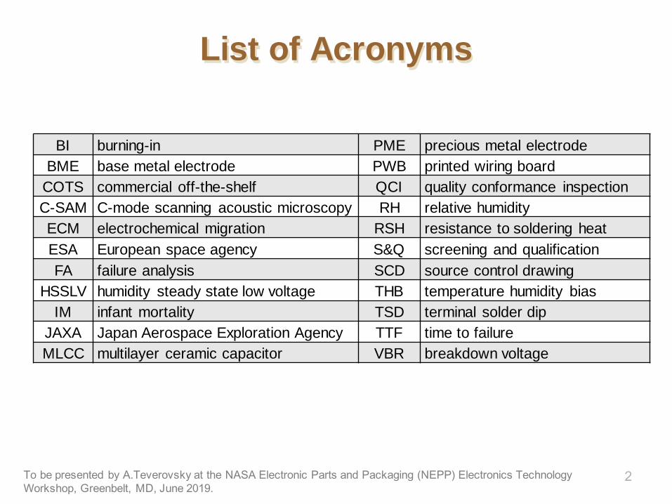
List of Acronyms
To be presented by A.Teverovsky at the NASA Electronic Parts and Packaging (NEPP) Electronics Technology Workshop, Greenbelt, MD, June 2019.
BI burning-in PME precious metal electrodeBME base metal electrode PWB printed wiring board
COTS commercial off-the-shelf QCI quality conformance inspectionC-SAM C-mode scanning acoustic microscopy RH relative humidityECM electrochemical migration RSH resistance to soldering heatESA European space agency S&Q screening and qualificationFA failure analysis SCD source control drawing
HSSLV humidity steady state low voltage THB temperature humidity biasIM infant mortality TSD terminal solder dip
JAXA Japan Aerospace Exploration Agency TTF time to failureMLCC multilayer ceramic capacitor VBR breakdown voltage
2
Abstract
To be presented by A.Teverovsky at the NASA Electronic Parts and Packaging (NEPP) Electronics Technology Workshop, Greenbelt, MD, June 2019.
3
This presentation gives a review of recent project failures caused by cracks in ceramic capacitors and discusses deficiencies of the existing screening and qualification procedures that can reveal the propensity to cracking and effects of soldering stresses.
Outline Recent history cases. Effect of hydrogen. A case when derating does not work. Defect-related infant mortality.
How different S&Q procedures assess the presence of cracks and address the effect of soldering? Military, space, and automotive industry requirements. Common mistakes. Manual soldering.
Conclusion
To be presented by A.Teverovsky at the NASA Electronic Parts and Packaging (NEPP) Electronics Technology Workshop, Greenbelt, MD, June 2019.
4
History Case 1
5To be presented by A.Teverovsky at the NASA Electronic Parts and Packaging (NEPP) Electronics Technology Workshop, Greenbelt, MD, June 2019.
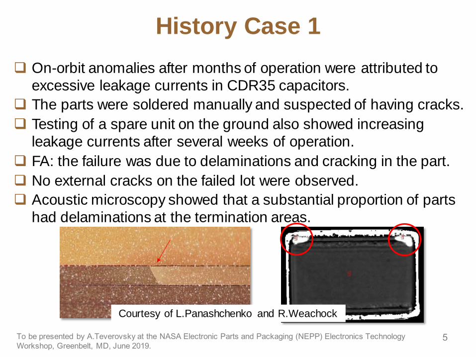
On-orbit anomalies after months of operation were attributed to excessive leakage currents in CDR35 capacitors.
The parts were soldered manually and suspected of having cracks. Testing of a spare unit on the ground also showed increasing
leakage currents after several weeks of operation. FA: the failure was due to delaminations and cracking in the part. No external cracks on the failed lot were observed. Acoustic microscopy showed that a substantial proportion of parts
had delaminations at the termination areas.
Courtesy of L.Panashchenko and R.Weachock
History Case 1, Delaminations
6To be presented by A.Teverovsky at the NASA Electronic Parts and Packaging (NEPP) Electronics Technology Workshop, Greenbelt, MD, June 2019.
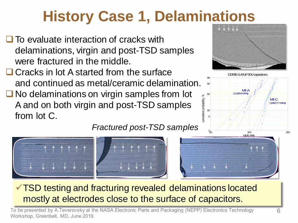
To evaluate interaction of cracks with delaminations, virgin and post-TSD samples were fractured in the middle.
Cracks in lot A started from the surface and continued as metal/ceramic delamination.
No delaminations on virgin samples from lot A and on both virgin and post-TSD samples from lot C.
TSD testing and fracturing revealed delaminations located mostly at electrodes close to the surface of capacitors.
Fractured post-TSD samples
CDR35 0.47uF 50V capacitors
MOR, MPa
cumu
lative
prob
abilit
y, %
50 2001001
5
10
50
90
99
Mfr.A
Mfr.C
(113/8.6 MPa)
(148/17.7 MPa)
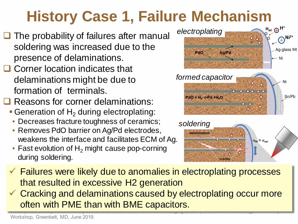
History Case 1, Failure Mechanism
7To be presented by A.Teverovsky at the NASA Electronic Parts and Packaging (NEPP) Electronics Technology Workshop, Greenbelt, MD, June 2019.
Failures were likely due to anomalies in electroplating processes that resulted in excessive H2 generation
Cracking and delaminations caused by electroplating occur more often with PME than with BME capacitors.
The probability of failures after manual soldering was increased due to the presence of delaminations.
Corner location indicates that delaminations might be due to formation of terminals.
Reasons for corner delaminations:Generation of H2 during electroplating:• Decreases fracture toughness of ceramics;• Removes PdO barrier on Ag/Pd electrodes,
weakens the interface and facilitates ECM of Ag.• Fast evolution of H2 might cause pop-corning
during soldering.
electroplating
formed capacitor
soldering
History Case 2
To be presented by A.Teverovsky at the NASA Electronic Parts and Packaging (NEPP) Electronics Technology Workshop, Greenbelt, MD, June 2019.
8
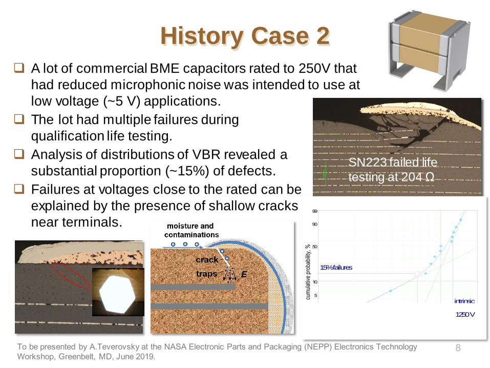
A lot of commercial BME capacitors rated to 250V that had reduced microphonic noise was intended to use at low voltage (~5 V) applications.
The lot had multiple failures during qualification life testing.
Analysis of distributions of VBR revealed a substantial proportion (~15%) of defects.
Failures at voltages close to the rated can be explained by the presence of shallow cracksnear terminals.
SN223 failed life testing at 204 Ω
XARM stack capacitors
breakdown voltage, V
cumu
lative
prob
abilit
y, %
100 200010001
5
10
50
90
99
DWV = 625V
15% failures
intrinsicVBR = 1250 V
History Case 2, Cont’d
To be presented by A.Teverovsky at the NASA Electronic Parts and Packaging (NEPP) Electronics Technology Workshop, Greenbelt, MD, June 2019.
9
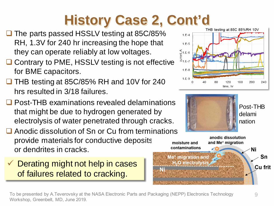
The parts passed HSSLV testing at 85C/85% RH, 1.3V for 240 hr increasing the hope that they can operate reliably at low voltages.
Contrary to PME, HSSLV testing is not effective for BME capacitors.
THB testing at 85C/85% RH and 10V for 240 hrs resulted in 3/18 failures.
Post-THB examinations revealed delaminationsthat might be due to hydrogen generated by electrolysis of water penetrated through cracks.
Anodic dissolution of Sn or Cu from terminations provide materials for conductive deposits or dendrites in cracks.
Post-THB delamination
Derating might not help in cases of failures related to cracking.
Probability - Weibull
time-to-failure, hr
cumu
lative
prob
ability
, %
1 10000010 100 1000 100001.E-2
5.E-2
1.E-1
5.E-1
1
5
10
50
90
99
1.E-2 x 6052
eta = 3.6E5 yearsbeta = 0.43
90% confidence bounds
History Case 3
To be presented by A.Teverovsky at the NASA Electronic Parts and Packaging (NEPP) Electronics Technology Workshop, Greenbelt, MD, June 2019.
10
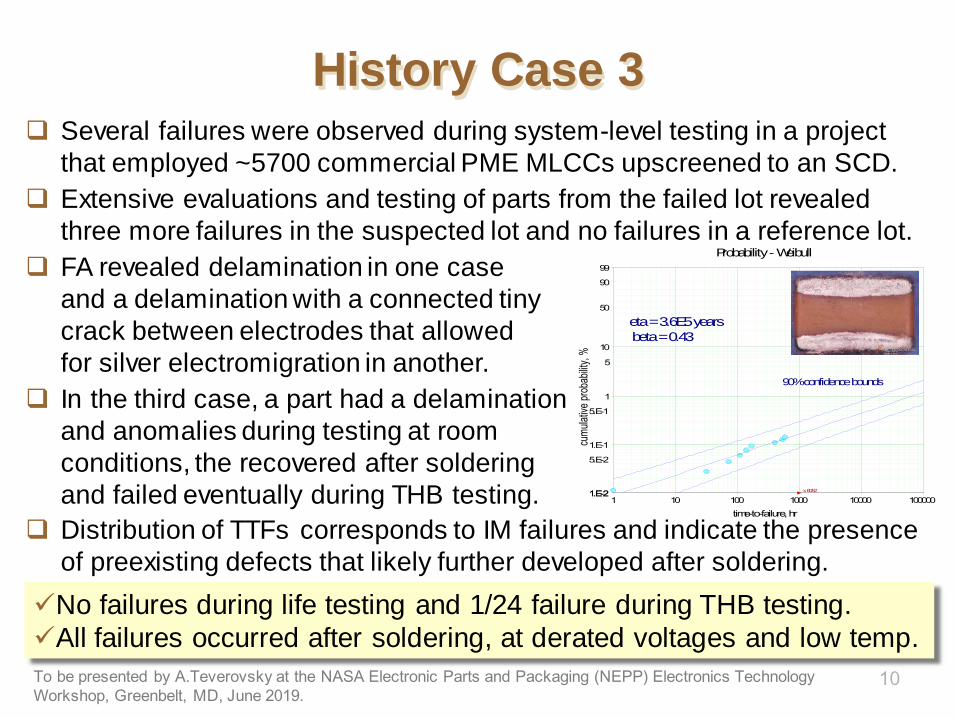
Several failures were observed during system-level testing in a project that employed ~5700 commercial PME MLCCs upscreened to an SCD.
Extensive evaluations and testing of parts from the failed lot revealed three more failures in the suspected lot and no failures in a reference lot.
FA revealed delamination in one case and a delamination with a connected tiny crack between electrodes that allowed for silver electromigration in another.
In the third case, a part had a delamination and anomalies during testing at room conditions, the recovered after soldering and failed eventually during THB testing.
Distribution of TTFs corresponds to IM failures and indicate the presence of preexisting defects that likely further developed after soldering.
No failures during life testing and 1/24 failure during THB testing.All failures occurred after soldering, at derated voltages and low temp.
History Case 3, Cont’d
To be presented by A.Teverovsky at the NASA Electronic Parts and Packaging (NEPP) Electronics Technology Workshop, Greenbelt, MD, June 2019.
11
Ag
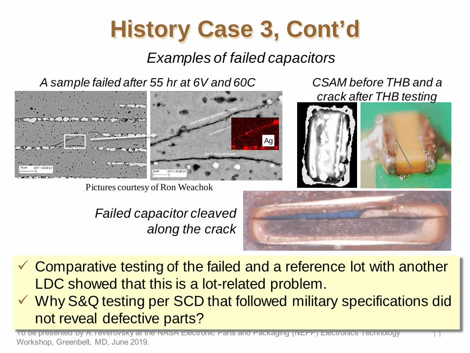
A sample failed after 55 hr at 6V and 60C
Comparative testing of the failed and a reference lot with another LDC showed that this is a lot-related problem.
Why S&Q testing per SCD that followed military specifications did not reveal defective parts?
Pictures courtesy of Ron Weachok
CSAM before THB and a crack after THB testing
Failed capacitor cleaved along the crack
Examples of failed capacitors
Risks of Humidity Testing
To be presented by A.Teverovsky at the NASA Electronic Parts and Packaging (NEPP) Electronics Technology Workshop, Greenbelt, MD, June 2019.
12
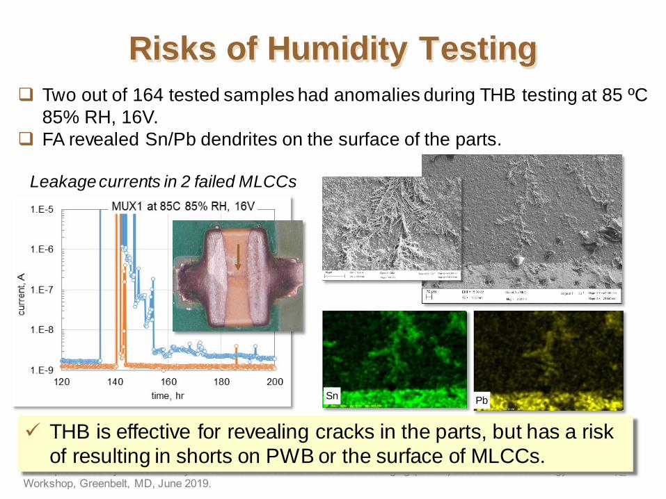
Two out of 164 tested samples had anomalies during THB testing at 85 ºC 85% RH, 16V.
FA revealed Sn/Pb dendrites on the surface of the parts.
Leakage currents in 2 failed MLCCs
THB is effective for revealing cracks in the parts, but has a risk of resulting in shorts on PWB or the surface of MLCCs.
Sn Pb
How Specifications Address Cracking and the Effect of Soldering?
To be presented by A.Teverovsky at the NASA Electronic Parts and Packaging (NEPP) Electronics Technology Workshop, Greenbelt, MD, June 2019.
13
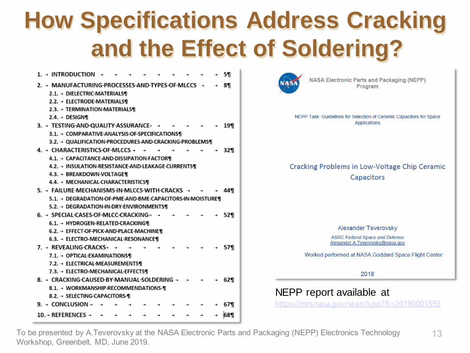
NEPP report available at https://ntrs.nasa.gov/search.jsp?R=20190001592
Comparison of Specifications
To be presented by A.Teverovsky at the NASA Electronic Parts and Packaging (NEPP) Electronics Technology Workshop, Greenbelt, MD, June 2019.
14
Specifications. Military: MIL-PRF-123, MIL-PRF-55681 (CDR-style), MIL-PRF-32535. Space: S-311-P829, S-311-P838, ESCC #3009, JAXA QTS-2040. Automotive: AEC-Q200.
Screening procedures. Difference in BI (MIL up to 264hr@2VR, ESA 96hr@2VR, JAXA: 21hr@ 3VR CSAM during screening: not used in M55681 and ESCC#3009. Gr. B: TS/life and THB not used in M55681 and ESCC#3009;
RSH: only in S-311-P838 and JAXA;HSSLV: only in M123, S-311-P-829, ESCC and JAXA.
Qualification procedures. TS cycles and SS from 100c/186pcs in M123 to 5c/18pcs in M55681. (Auto-1kc). No RSH requirements for ESCC#3009. Flex testing is not required for M123 and ESCC#3009. Requirements for life and humidity testing are relaxed for some data sheet
numbers in M32535. JAXA approach: automotive grade BME MLCCs are solder dipped,
screened by CSAM, BI and derated. Periodical QCI (relaxed voltage stress for thin dielectric capacitors) and extensive additional testing.
Soldering Stresses during Qualification
To be presented by A.Teverovsky at the NASA Electronic Parts and Packaging (NEPP) Electronics Technology Workshop, Greenbelt, MD, June 2019.
15
Mounting before testing. M123 does not specify mounting before qualification testing. M55681 does not have mounting requirements for life or HSSLV testing. M32535: mounting for humidity testing is optional. S-311-P-829 does not have mounting requirements at all and P-838 does
not require soldering before life testing.Warning: “the substrate and mounting process shall be such that it will not be
the cause of, nor contribute to, failure of any test for which it may be used”.
Resistance to soldering heat. The test should verify the robustness of MLCCs against soldering
stresses and simulate the worst case soldering conditions. MIL-STD-202 TM210 specifies 8 versions of the test. Only two and at
relaxed requirements are used (solder dip for M123 and IR reflow for M55681). Commercial parts are tested at much higher temperatures.
Soldering iron test that can simulate manual soldering is not used.
Sample Size and Typical Misconceptions
To be presented by A.Teverovsky at the NASA Electronic Parts and Packaging (NEPP) Electronics Technology Workshop, Greenbelt, MD, June 2019.
16
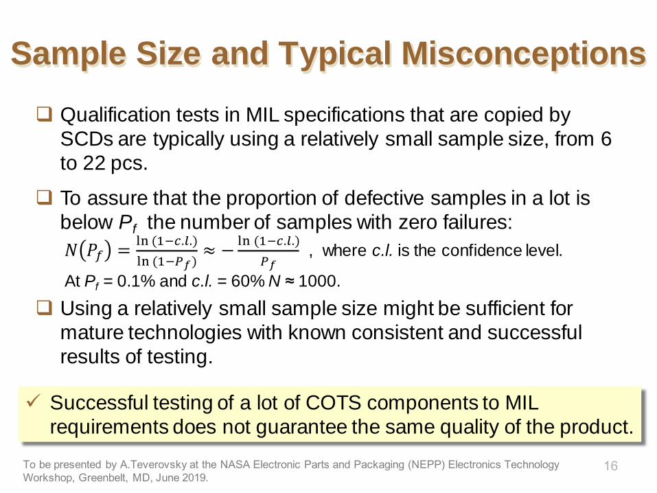
Qualification tests in MIL specifications that are copied by SCDs are typically using a relatively small sample size, from 6 to 22 pcs.
To assure that the proportion of defective samples in a lot is below Pf the number of samples with zero failures:𝑁𝑁 𝑃𝑃𝑓𝑓 = ln (1−𝑐𝑐.𝑙𝑙.)
ln (1−𝑃𝑃𝑓𝑓)≈ − ln (1−𝑐𝑐.𝑙𝑙.)
𝑃𝑃𝑓𝑓, where c.l. is the confidence level.
At Pf = 0.1% and c.l. = 60% N ≈ 1000. Using a relatively small sample size might be sufficient for
mature technologies with known consistent and successful results of testing.
Successful testing of a lot of COTS components to MIL requirements does not guarantee the same quality of the product.
Susceptibility to Cracking during Manual Soldering
To be presented by A.Teverovsky at the NASA Electronic Parts and Packaging (NEPP) Electronics Technology Workshop, Greenbelt, MD, June 2019.
17
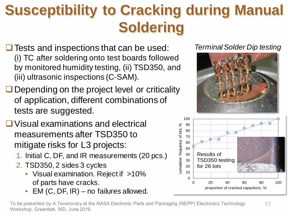
Tests and inspections that can be used: (i) TC after soldering onto test boards followed by monitored humidity testing, (ii) TSD350, and (iii) ultrasonic inspections (C-SAM).
Depending on the project level or criticality of application, different combinations of tests are suggested.
Visual examinations and electrical measurements after TSD350 to mitigate risks for L3 projects:1. Initial C, DF, and IR measurements (20 pcs.)2. TSD350, 2 sides 3 cycles
• Visual examination. Reject if >10% of parts have cracks.
• EM (C, DF, IR) – no failures allowed.
0102030405060708090
100
0 20 40 60 80 100cu
mula
tive
frequ
ency
of l
ots,
%
proportion of cracked capacitors, %
Results of TSD350 testing for 26 lots
Terminal Solder Dip testing
Conclusion
To be presented by A.Teverovsky at the NASA Electronic Parts and Packaging (NEPP) Electronics Technology Workshop, Greenbelt, MD, June 2019.
18
Cracking remains the major cause of MLCCs’ failures in space instruments.
Cracking is due to a combination of built-in internal stresses, manufacturing defects and external, soldering-related stresses.
The most popular, CDR-style MLCCs are not screened by C-SAM and do not have requirements for mounting during qualification.
Existing specifications are focused mostly on quality of as build capacitors and do not address properly effects of soldering.
S&Q of commercial MLCCs to MIL-like SCDs does not assure the same quality of the parts.
Procedures to mitigate risks of manual soldering and select the most robust parts are suggested.