Embed Size (px)
Citation preview
MIKRONIEK IS A PUBLICATION OF THE DUTCH SOCIETY FOR PRECISION ENGINEERING WWW.DSPE.NL
PROFESSIONAL JOURNAL ON PRECISION ENGINEERING2017 (VOL. 57) ISSUE 4
THEME: OPTOMECHATRONICS OPTICS WEEK 2017 PREVIEW MECHATRONICS FORUM REPORT VIRTUAL AFM CALIBRATION STANDARDS
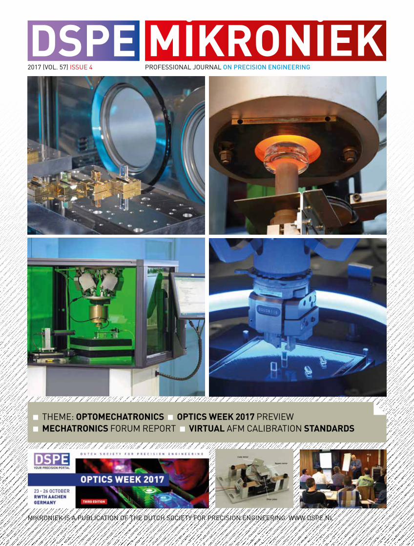
VDL Enabling Technologies Group
De Schakel 22 • 5651 GH Eindhoven • The Netherlands
Phone: +31 (0)40 263 88 88 • [email protected] • www.vdletg.com
EVER WONDERED HOW CLEAN A ‘CLEAN’ PRODUCT IS?
This is an important question for VDL ETG. We deliver systems to our partners operating in
markets like semiconductor, analytical, medical, solar and science & technology. Highly
demanding markets which require (ultra) precision technology and minimal contamination.
VDL ETG is world class in the design, development and production of extreme clean modules
and systems for our partners. Already in an early stage of our product generation process the
cleanliness of our products is an important requirement. The process at VDL ETG is arranged in
such way that it meets the highest cleanliness standards from our partners. Investing both in
cleanliness research and world class cleanliness manufacturing VDL ETG ensures that the next
step in technology will be enabled.
(VACUUM) WAFER HANDLERS
(VACUUM) WAFER STAGES
(VACUUM) PROCESS CHAMBERS
RF ACCELERATOR STRUCTURES
X-RAY MEDICAL EQUIPMENT
FLEXIBLE SUBSTRATE ELECTRONICS
CVD EQUIPMENT
E-BEAM COLUMNS
AND MORE…
VDL Enabling Technologies Group
RF accelerator structure
VDL_ETG_Adv_225x297_2017-07_DEF.indd 1 25-07-17 09:10
IN THIS ISSUEPUBLICATION INFORMATION ISSUE2017 4
ObjectiveProfessional journal on precision engineering and the official organ of DSPE, the Dutch Society for Precision Engineering. Mikroniek provides current information about scientific, technical and business developments in the fields of precision engineering, mechatronics and optics.The journal is read by researchers and professionals in charge of the development and realisation of advanced precision machinery.
PublisherDSPEAnnemarie SchrauwenHigh Tech Campus 1, 5656 AE EindhovenPO Box 80036, 5600 JW [email protected], www.dspe.nl
Editorial boardProf.dr.ir. Just Herder (chairman, Delft University of Technology, University of Twente), ir.ing. Bert Brals (Sioux Mechatronics), dr.ir. Dannis Brouwer (University of Twente), Maarten Dekker, M.Sc. (Demcon), ir. Henk Kiela (Opteq, Fontys), ir. Casper Kruijer, MBI (Thermo Fisher Scientific), ing. Ronald Lamers, M.Sc. (MI-Partners), Erik Manders, M.Sc. (Philips Innovation Services), dr.ir. Gerrit Oosterhuis (VDL ETG), Maurice Teuwen, M.Sc. (Janssen Precision Engineering)
EditorHans van Eerden, [email protected]
Advertising canvasserGerrit Kulsdom, Sales & Services+31 (0)229 – 211 211, [email protected]
Design and realisationDrukkerij Snep, Eindhoven+31 (0)40 – 251 99 29, [email protected]
SubscriptionMikroniek is for DSPE members only. DSPE membership is open to institutes, companies, self-employed professionals and private persons, and starts at € 80.00 (excl. VAT) per year.
Mikroniek appears six times a year.© Nothing from this publication may be reproduced or copied without the express permission of the publisher.
ISSN 0026-3699
Theme: Optomechatronics
05DSPE Optics Week 2017 crosses disciplinary and geographical bordersThe third edition of the DSPE Optics Week will take place in Aachen (Germany). The 4-day event, from 23 to 26 October, comprises a symposium & fair, a demonstration day and two high-level optics courses.
10Harnessing the next generation of extremely large telescopesVersatile test control systems designed by S[&]T are used to prove that the warping harnesses for the next generation of extremely large telescopes meet the specifications.
16A new word for an old problemReflections on teaching optomechanics by Daniel Vukobratovich.
18Optical fibre interferometry – new concepts and applicationsOptics11 has developed new measurement concepts based on optical fibre interferometry, creating new opportunities in sensing.
23Exporting Dutch optomechatronics to ChinaNew opportunities for the Nanomefos freeform optics measurement machine.
26Getting a grip on medical and modular roboticsReport of the Saxion Mechatronics Forum on modular building blocks for robotic systems.
32Virtual standards, real advantagesVSL presents a smart calibration solution for inline atomic force microscopy.
26
23
FEATURES04 EDITORIALPaul Urbach, Professor in Optics at Delft University of Technology, on new developments in Dutch optics and optomechatronics.
39 TAPPING INTO A NEW DSPE MEMBER’S EXPERTISE
TEN Flecs – contract manufacturer for thinfilm products.
40 ECP2 COURSE CALENDAROverview of European Certified Precision Engineering courses.
41 UPCOMING EVENTSIncluding: LiS Academy Manufacturability course.
42 NEWSIncluding: EMO preview.
The main cover photos (representing projects featured at the Demonstration Day of the DSPE Optics Week 2017) are courtesy of Fraunhofer ILT and IPT. Read the preview on page 5 ff.
nr 4 2017 MIKRONIEK 3
EDITORIAL
Optomechatronics, the fusion of optics with mechanics, electronics and software, is essential for high-tech optical instruments. High-speed scanning of focused spots, adaptive optics with deformable mirrors and atomic force microscopy are only a few examples out of many.
Since there are very few educational programmes in optomechatronics, engineers working in the field typically have either a master in optics or in mechanics, and then have to acquire their knowledge of the other discipline on the job. But this situation will soon improve. The Faculty of Mechanical, Maritime and Materials Engineering (3mE) of Delft University of Technology (TU Delft) will start a Master track in optomechatronics with the aim to educate a new generation of multidisciplinary engineers.
And there are more new developments related to optics and optomechatronics. Recently, the Dutch Optics Centre (DOC) has been installed by TU Delft and TNO. The aims of DOC are: 1 to increase the industrial impact of research and development in the fields of optical imaging, metrology
and spectroscopy, by involving industrial partners in research projects at an early stage and by carrying out high-TRL (technology readiness level) projects together with industry;
2. to foster and stimulate education and training in optics and optomechanics of students and of people in industry;
3. to share facilities.
DOC builds on a long tradition in optics and optomechatronics of TU Delft and TNO. The Van Leeuwenhoek Laboratory, which they founded, contains advanced equipment for nanofabrication. Furthermore, TNO houses a high-quality manufacturing facility for freeform optics.
Although started by TU Delft and TNO, DOC is not restricted to Delft research groups. Projects with partners from other universities in the Netherlands will be started. Companies can participate for free in DOC by using the contact button on www.doc.com. They will then receive invitations for DOC meetings, brainstorm sessions and network events.
To efficiently represent the interests of the Dutch optical community and to speak with one voice in contacts with governmental and funding agencies, DOC will collaborate with PhotonicsNL, DSPE, and PhotonDelta, the ecosystem initiated by Eindhoven University of Technology that specialises in integrated photonics, i.e., in optics on a chip.
The upcoming Optics Week, organised by DSPE, has become the major biennial event for optomechatronics in the Netherlands, and beyond. This year it is held from 23 to 26 October in Aachen, Germany. Apart from a symposium and a fair, a visit to the Fraunhofer Institute in Aachen is scheduled and courses in optomechanics and optical design will be given. More detailed information about this eventful week can be found in this issue of Mikroniek.
I hope to see you in Aachen!
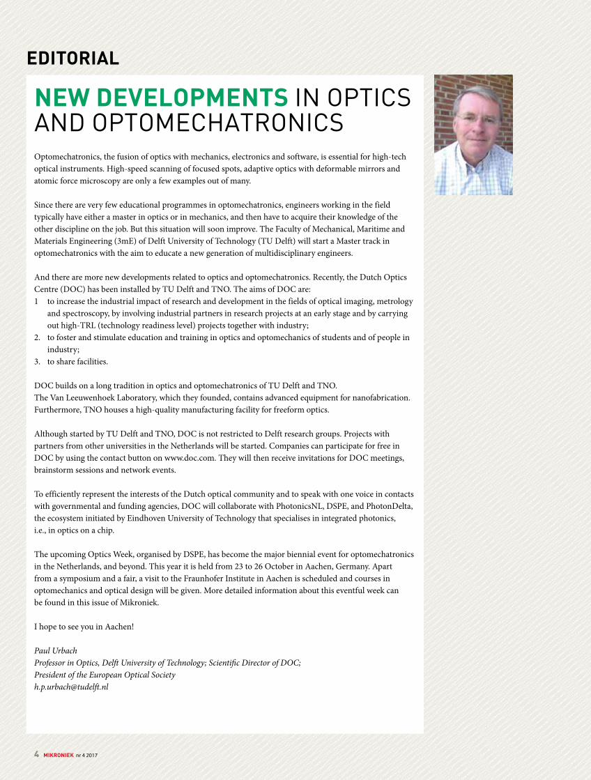
Paul UrbachProfessor in Optics, Delft University of Technology; Scientific Director of DOC; President of the European Optical [email protected]
NEW DEVELOPMENTS IN OPTICS AND OPTOMECHATRONICS
4 MIKRONIEK nr 4 2017
THIRD EDITION OF DSPE OPTICS WEEK TAKES PLACE IN AACHEN, GERMANY
CROSSING DISCIPLINARY AND GEOGRAPHICAL BORDERS
The third ever DSPE Optics Week will be held in the German city of Aachen on 23-26 October 2017. The 4-day event will include a symposium and fair, a demonstration day and two high-level optics courses. This year will be the first time the multidisciplinary event that combines optics and mechatronics also crosses geographical borders.
The DSPE Optics Week 2017 is a unique collaboration by Dutch, German and international organisations. The third edition of the biennial event will be held on 23-26 October at the RWTH Aachen University, Germany
(Figure 1). The 4-day event will bring together outstanding international speakers and lecturers from a variety of backgrounds, ranging from semiconductors and the medical profession to other industries and academia.
DSPE initiativeThe event debuted in 2013, with the one-day DSPE Optics and Optomechatronics Symposium in Eindhoven, the Netherlands. The second edition in 2015 in Delft, the Netherlands included two courses on optics as well as the symposium. Both events attracted more than 250 precision engineers. “To extend our scope abroad, we decided to organise the DSPE Optics Week 2017 in the German city of Aachen and to involve representatives from renowned German companies and institutes”, says DSPE president Hans Krikhaar. “Home to the Fraunhofer Institutes IPT (production technology) and ILT (laser technology), as well as the RWTH research university, Aachen is a hotspot for every facet of the optics industry and ideally located close to the Dutch border. We want to strengthen the relationship between the Dutch and German precision engineering and optics communities
Symposium & FairThe 4-day event kicks off on Monday, 23 October with the DSPE Optics and Optomechanics Symposium & Fair. As chairman for the day, Jos Benschop, Senior Vice President Technology at ASML (Figure 2), will preside over the presentation of a range of topics, including the 3D printing of optical components, as well as adaptive optics, thermal effects in optical systems, and complex optical coatings. Speakers will be from various companies, including Demcon Focal, Fraunhofer, PTB, Qioptiq, TNO and Zeiss SMT.
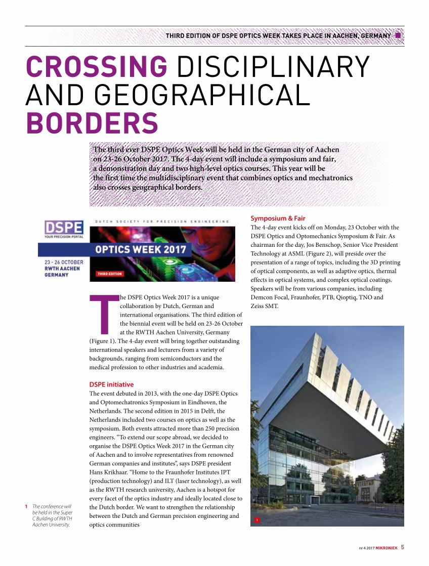
1 The conference will be held in the Super C Building of RWTH Aachen University.
1
nr 4 2017 MIKRONIEK 5
THIRD EDITION OF DSPE OPTICS WEEK TAKES PLACE IN AACHEN, GERMANY
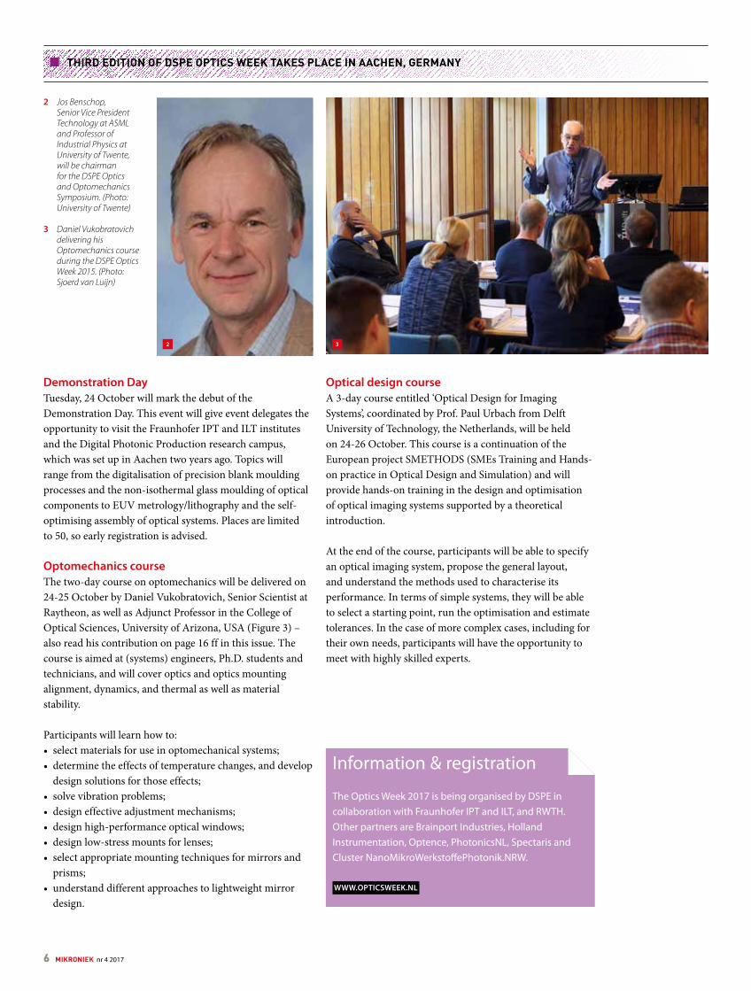
2 Jos Benschop, Senior Vice President Technology at ASML and Professor of Industrial Physics at University of Twente, will be chairman for the DSPE Optics and Optomechanics Symposium. (Photo: University of Twente)
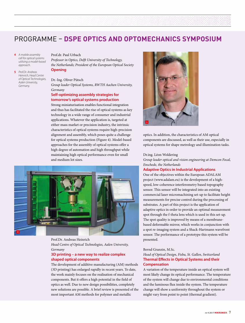
3 Daniel Vukobratovich delivering his Optomechanics course during the DSPE Optics Week 2015. (Photo: Sjoerd van Luijn)
Demonstration DayTuesday, 24 October will mark the debut of the Demonstration Day. This event will give event delegates the opportunity to visit the Fraunhofer IPT and ILT institutes and the Digital Photonic Production research campus, which was set up in Aachen two years ago. Topics will range from the digitalisation of precision blank moulding processes and the non-isothermal glass moulding of optical components to EUV metrology/lithography and the self-optimising assembly of optical systems. Places are limited to 50, so early registration is advised.
Optomechanics courseThe two-day course on optomechanics will be delivered on 24-25 October by Daniel Vukobratovich, Senior Scientist at Raytheon, as well as Adjunct Professor in the College of Optical Sciences, University of Arizona, USA (Figure 3) – also read his contribution on page 16 ff in this issue. The course is aimed at (systems) engineers, Ph.D. students and technicians, and will cover optics and optics mounting alignment, dynamics, and thermal as well as material stability.
Participants will learn how to:• select materials for use in optomechanical systems;• determine the effects of temperature changes, and develop
design solutions for those effects;• solve vibration problems;• design effective adjustment mechanisms;• design high-performance optical windows;• design low-stress mounts for lenses;• select appropriate mounting techniques for mirrors and
prisms;• understand different approaches to lightweight mirror
design.
Optical design courseA 3-day course entitled ‘Optical Design for Imaging Systems’, coordinated by Prof. Paul Urbach from Delft University of Technology, the Netherlands, will be held on 24-26 October. This course is a continuation of the European project SMETHODS (SMEs Training and Hands-on practice in Optical Design and Simulation) and will provide hands-on training in the design and optimisation of optical imaging systems supported by a theoretical introduction.
At the end of the course, participants will be able to specify an optical imaging system, propose the general layout, and understand the methods used to characterise its performance. In terms of simple systems, they will be able to select a starting point, run the optimisation and estimate tolerances. In the case of more complex cases, including for their own needs, participants will have the opportunity to meet with highly skilled experts.
2 3
Information & registration
The Optics Week 2017 is being organised by DSPE in collaboration with Fraunhofer IPT and ILT, and RWTH. Other partners are Brainport Industries, Holland Instrumentation, Optence, PhotonicsNL, Spectaris and Cluster NanoMikroWerkstoffePhotonik.NRW.
WWW.OPTICSWEEK.NL
6 MIKRONIEK nr 4 2017
Prof.dr. Paul UrbachProfessor in Optics, Delft University of Technology, the Netherlands; President of the European Optical SocietyOpening
Dr.-Ing. Oliver PütschGroup leader Optical Systems, RWTH Aachen University, GermanySelf-optimizing assembly strategies for tomorrow’s optical systems productionStrong miniaturisation enables functional integration and thus has facilitated the rise of optical systems as key technology in a wide range of consumer and industrial applications. Whatever the application is, targeted at either mass market or precision industry, the intrinsic characteristics of optical systems require high-precision alignment and assembly, which poses quite a challenge for optical systems production (Figure 4). Model-based approaches for the assembly of optical systems offer a high degree of automation and high throughput while maintaining high optical performance even for small and medium lot sizes.
Prof.Dr. Andreas HeinrichHead Centre of Optical Technologies, Aalen University, Germany3D printing – a new way to realize complex shaped optical componentsThe development of additive manufacturing (AM) methods (3D printing) has enlarged rapidly in recent years. To date, the work mainly focuses on the realisation of mechanical components. But it offers a high potential in the field of optics as well. Due to new design possibilities, completely new solutions are possible. A brief review is presented of the most important AM methods for polymer and metallic
optics. In addition, the characteristics of AM optical components are discussed, as well as their use, especially in optical systems for shape metrology and illumination tasks.
Dr.ing. Léon WolderingGroup leader optical and vision engineering at Demcon Focal, Enschede, the NetherlandsAdaptive Optics in Industrial ApplicationsOne of the objectives within the European ADALAM project (www.adalam.eu) is the development of a high-speed, low-coherence interferometry based topography sensor. This sensor will be integrated into an existing commercial laser micromachining set-up to facilitate height measurements for precise control during the processing of substrates. A part of this project is the application of adaptive optics in order to provide an optimal measurement spot through the f-theta lens which is used in this set-up. The spot quality is improved by means of a membrane-based deformable mirror, which works in conjunction with a spot re-imaging system and a Shack-Hartmann wavefront sensor. The performance of a prototype this system will be presented.
Bernd Granzin, M.Sc.Head of Optical Design, Fisba, St. Gallen, SwitzerlandThermal Effects in Optical Systems and their CompensationA variation of the temperature inside an optical system will most likely change its optical performance. The temperature of the system will change due to environmental conditions and the luminous flux inside the system. The temperature change will show a uniformity throughout the system or might vary from point to point (thermal gradient).
4 A mobile assembly cell for optical systems utilising a model-based approach.
5 Prof.Dr. Andreas Heinrich, Head Centre of Optical Technologies, Aalen University, Germany.
4
5
PROGRAMME – DSPE OPTICS AND OPTOMECHANICS SYMPOSIUM
nr 4 2017 MIKRONIEK 7
THIRD EDITION OF DSPE OPTICS WEEK TAKES PLACE IN AACHEN, GERMANY
The prime thermal effect in optical systems is mostly a shift of the focal plane. An introductory overview of thermal effects in optical systems and their origins will be given. Some basic methods for compensation will be discussed as well.
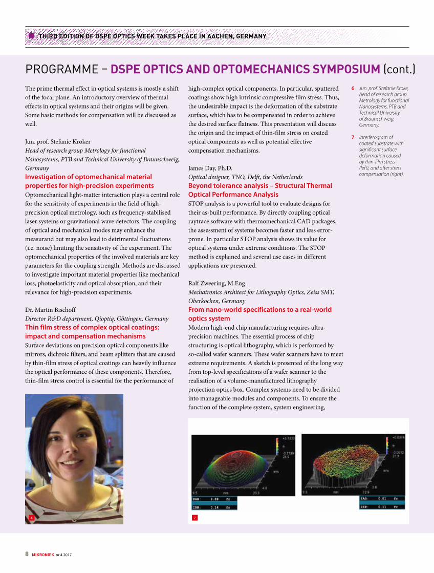
Jun. prof. Stefanie KrokerHead of research group Metrology for functional Nanosystems, PTB and Technical University of Braunschweig, GermanyInvestigation of optomechanical material properties for high-precision experimentsOptomechanical light-matter interaction plays a central role for the sensitivity of experiments in the field of high-precision optical metrology, such as frequency-stabilised laser systems or gravitational wave detectors. The coupling of optical and mechanical modes may enhance the measurand but may also lead to detrimental fluctuations (i.e. noise) limiting the sensitivity of the experiment. The optomechanical properties of the involved materials are key parameters for the coupling strength. Methods are discussed to investigate important material properties like mechanical loss, photoelasticity and optical absorption, and their relevance for high-precision experiments.
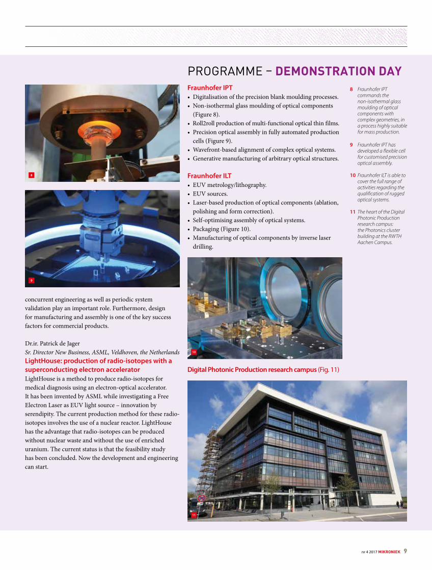
Dr. Martin BischoffDirector R&D department, Qioptiq, Göttingen, GermanyThin film stress of complex optical coatings: impact and compensation mechanismsSurface deviations on precision optical components like mirrors, dichroic filters, and beam splitters that are caused by thin-film stress of optical coatings can heavily influence the optical performance of these components. Therefore, thin-film stress control is essential for the performance of
high-complex optical components. In particular, sputtered coatings show high intrinsic compressive film stress. Thus, the undesirable impact is the deformation of the substrate surface, which has to be compensated in order to achieve the desired surface flatness. This presentation will discuss the origin and the impact of thin-film stress on coated optical components as well as potential effective compensation mechanisms.
James Day, Ph.D.Optical designer, TNO, Delft, the NetherlandsBeyond tolerance analysis – Structural Thermal Optical Performance Analysis STOP analysis is a powerful tool to evaluate designs for their as-built performance. By directly coupling optical raytrace software with thermomechanical CAD packages, the assessment of systems becomes faster and less error-prone. In particular STOP analysis shows its value for optical systems under extreme conditions. The STOP method is explained and several use cases in different applications are presented.
Ralf Zweering, M.Eng.Mechatronics Architect for Lithography Optics, Zeiss SMT, Oberkochen, GermanyFrom nano-world specifications to a real-world optics systemModern high-end chip manufacturing requires ultra-precision machines. The essential process of chip structuring is optical lithography, which is performed by so-called wafer scanners. These wafer scanners have to meet extreme requirements. A sketch is presented of the long way from top-level specifications of a wafer scanner to the realisation of a volume-manufactured lithography projection optics box. Complex systems need to be divided into manageable modules and components. To ensure the function of the complete system, system engineering,
6 Jun. prof. Stefanie Kroke, head of research group Metrology for functional Nanosystems, PTB and Technical University of Braunschweig, Germany.
7 Interferogram of coated substrate with significant surface deformation caused by thin-film stress (left), and after stress compensation (right).
6 7
PROGRAMME – DSPE OPTICS AND OPTOMECHANICS SYMPOSIUM (cont.)
8 MIKRONIEK nr 4 2017
concurrent engineering as well as periodic system validation play an important role. Furthermore, design for manufacturing and assembly is one of the key success factors for commercial products.
Dr.ir. Patrick de JagerSr. Director New Business, ASML, Veldhoven, the NetherlandsLightHouse: production of radio-isotopes with a superconducting electron acceleratorLightHouse is a method to produce radio-isotopes for medical diagnosis using an electron-optical accelerator. It has been invented by ASML while investigating a Free Electron Laser as EUV light source – innovation by serendipity. The current production method for these radio-isotopes involves the use of a nuclear reactor. LightHouse has the advantage that radio-isotopes can be produced without nuclear waste and without the use of enriched uranium. The current status is that the feasibility study has been concluded. Now the development and engineering can start.
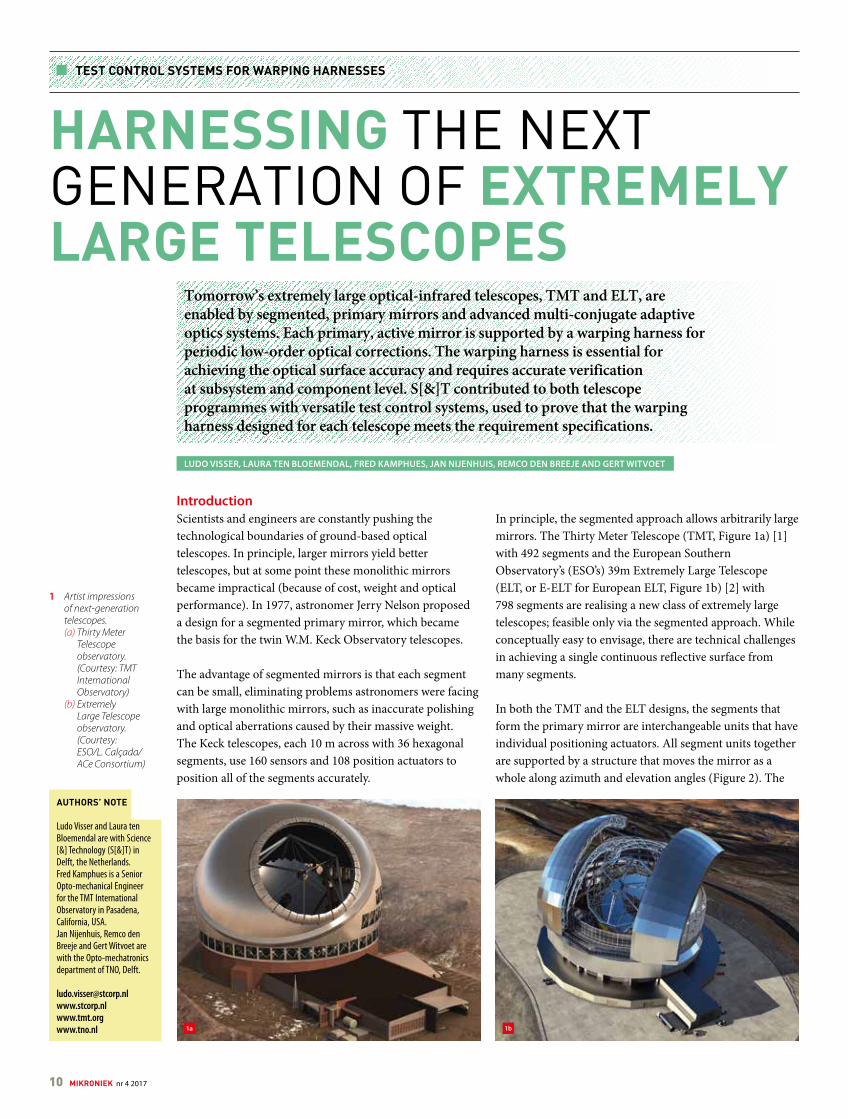
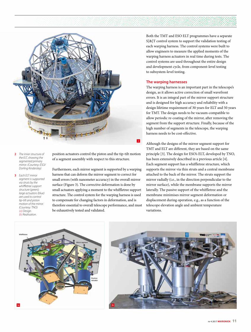
Fraunhofer IPT• Digitalisation of the precision blank moulding processes.• Non-isothermal glass moulding of optical components
(Figure 8).• Roll2roll production of multi-functional optical thin films.• Precision optical assembly in fully automated production
cells (Figure 9).• Wavefront-based alignment of complex optical systems.• Generative manufacturing of arbitrary optical structures.
Fraunhofer ILT• EUV metrology/lithography.• EUV sources.• Laser-based production of optical components (ablation,
polishing and form correction).• Self-optimising assembly of optical systems.• Packaging (Figure 10).• Manufacturing of optical components by inverse laser
drilling.
Digital Photonic Production research campus (Fig. 11)
PROGRAMME – DEMONSTRATION DAY
11
8 Fraunhofer IPT commands the non-isothermal glass moulding of optical components with complex geometries, in a process highly suitable for mass production.
9 Fraunhofer IPT has developed a flexible cell for customised precision optical assembly.
10 Fraunhofer ILT is able to cover the full range of activities regarding the qualification of rugged optical systems.
11 The heart of the Digital Photonic Production research campus: the Photonics cluster building at the RWTH Aachen Campus.
10
8
9
nr 4 2017 MIKRONIEK 9
TEST CONTROL SYSTEMS FOR WARPING HARNESSES
HARNESSING THE NEXT GENERATION OF EXTREMELY LARGE TELESCOPES
Tomorrow’s extremely large optical-infrared telescopes, TMT and ELT, are enabled by segmented, primary mirrors and advanced multi-conjugate adaptive optics systems. Each primary, active mirror is supported by a warping harness for periodic low-order optical corrections. The warping harness is essential for achieving the optical surface accuracy and requires accurate verification at subsystem and component level. S[&]T contributed to both telescope programmes with versatile test control systems, used to prove that the warping harness designed for each telescope meets the requirement specifications.
IntroductionScientists and engineers are constantly pushing the technological boundaries of ground-based optical telescopes. In principle, larger mirrors yield better telescopes, but at some point these monolithic mirrors became impractical (because of cost, weight and optical performance). In 1977, astronomer Jerry Nelson proposed a design for a segmented primary mirror, which became the basis for the twin W.M. Keck Observatory telescopes.
The advantage of segmented mirrors is that each segment can be small, eliminating problems astronomers were facing with large monolithic mirrors, such as inaccurate polishing and optical aberrations caused by their massive weight. The Keck telescopes, each 10 m across with 36 hexagonal segments, use 160 sensors and 108 position actuators to position all of the segments accurately.
LUDO VISSER, LAURA TEN BLOEMENDAL, FRED KAMPHUES, JAN NIJENHUIS, REMCO DEN BREEJE AND GERT WITVOET
AUTHORS’ NOTE
Ludo Visser and Laura ten Bloemendal are with Science [&] Technology (S[&]T) in Delft, the Netherlands. Fred Kamphues is a Senior Opto-mechanical Engineer for the TMT International Observatory in Pasadena, California, USA. Jan Nijenhuis, Remco den Breeje and Gert Witvoet are with the Opto-mechatronics department of TNO, Delft.
In principle, the segmented approach allows arbitrarily large mirrors. The Thirty Meter Telescope (TMT, Figure 1a) [1] with 492 segments and the European Southern Observatory’s (ESO’s) 39m Extremely Large Telescope (ELT, or E-ELT for European ELT, Figure 1b) [2] with 798 segments are realising a new class of extremely large telescopes; feasible only via the segmented approach. While conceptually easy to envisage, there are technical challenges in achieving a single continuous reflective surface from many segments.
In both the TMT and the ELT designs, the segments that form the primary mirror are interchangeable units that have individual positioning actuators. All segment units together are supported by a structure that moves the mirror as a whole along azimuth and elevation angles (Figure 2). The
1 Artist impressions of next-generation telescopes.
(a) Thirty Meter Telescope observatory. (Courtesy: TMT International Observatory)
(b) Extremely Large Telescope observatory. (Courtesy: ESO/L. Calçada/ACe Consortium)
1b1a
10 MIKRONIEK nr 4 2017
2 The inner structure of the ELT, showing the segmented primary mirror. (Courtesy: ESO/Dorling Kindersley)
3 Each ELT mirror segment is supported via struts by the whiffletree support structure (green); large actuators (blue) are used to control tip-tilt and piston motion of the mirror. (Courtesy: TNO)
(a) Design. (b) Realisation.
position actuators control the piston and the tip-tilt motion of a segment assembly with respect to this structure.
Furthermore, each mirror segment is supported by a warping harness that can deform the mirror segment to correct for small errors (with nanometer accuracy) in the overall mirror surface (Figure 3). The corrective deformation is done by small actuators applying a moment to the whiffletree support structure. The control system for the warping harness is used to compensate for changing factors in deformation, and is therefore essential to overall telescope performance, and must be exhaustively tested and validated.
Both the TMT and ESO ELT programmes have a separate S[&]T control system to support the validation testing of each warping harness. The control systems were built to allow engineers to measure the applied moments of the warping harness actuators in real time during tests. The control systems are used throughout the entire design and development cycle, from component-level testing to subsystem-level testing.
The warping harnessesThe warping harness is an important part in the telescope’s design, as it allows active correction of small wavefront errors. It is an integral part of the mirror support structure and is designed for high accuracy and reliability with a design lifetime requirement of 30 years for ELT and 50 years for TMT. The design needs to be vacuum-compatible to allow periodic re-coating of the mirror, after removing the segment from the support structure. Finally, because of the high number of segments in the telescope, the warping harness needs to be cost-effective.
Although the designs of the mirror segment support for TMT and ELT are different, they are based on the same principle [3]. The design for ESO’s ELT, developed by TNO, has been extensively described in a previous article [4]. Each segment support has a whiffletree structure, which supports the mirror via thin struts and a central membrane attached to the back of the mirror. The struts support the mirror radially (i.e., in the direction perpendicular to the mirror surface), while the membrane supports the mirror laterally. The passive support of the whiffletree and the membrane minimises mirror segment deformation or displacement during operation, e.g., as a function of the telescope elevation angle and ambient temperature variations.
2
3a 3b
nr 4 2017 MIKRONIEK 11
TEST CONTROL SYSTEMS FOR WARPING HARNESSES
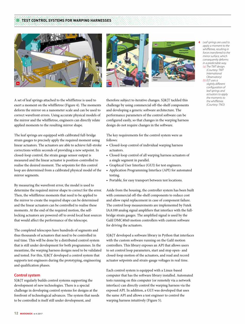
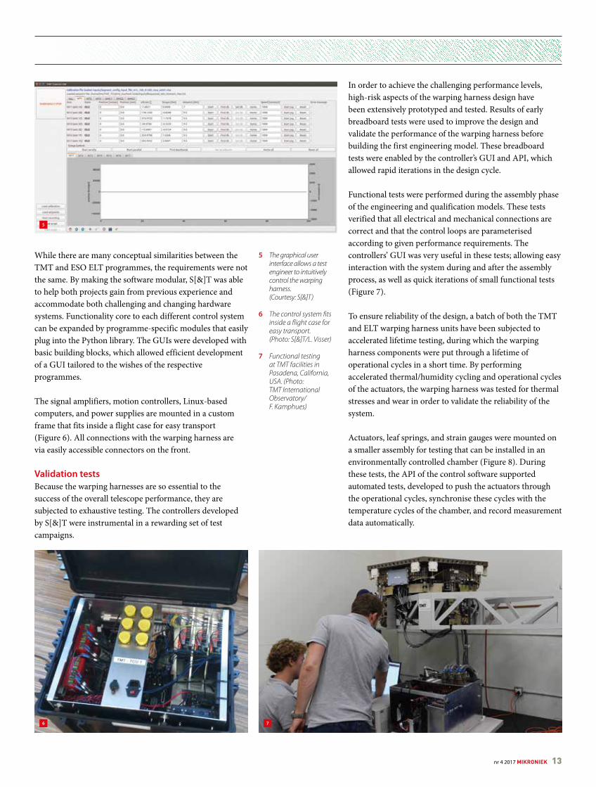
A set of leaf springs attached to the whiffletree is used to exert a moment on the whiffletree (Figure 4). The moments deform the mirror on a nanometer scale and can be used to correct wavefront errors. Using accurate physical models of the mirror and the whiffletree, engineers can directly relate applied moments to the resulting mirror shape.
The leaf springs are equipped with calibrated full-bridge strain gauges to precisely apply the required moment using linear actuators. The actuators are able to achieve full-stroke corrections within seconds of providing a new setpoint. In closed-loop control, the strain gauge sensor output is measured and the linear actuator is position-controlled to realise the desired moment. The setpoints for this control loop are determined from a calibrated physical model of the mirror segments.
By measuring the wavefront error, the model is used to determine the required mirror shape to correct for the error. Then, the whiffletree moments that need to be applied to the mirror to create the required shape can be determined and the linear actuators can be controlled to realise these moments. At the end of the required motion, the self-locking actuators are powered off to avoid local heat sources that would affect the performance of the telescope.
The completed telescopes have hundreds of segments and thus thousands of actuators that need to be controlled in real time. This will be done by a distributed control system that is still under development for both programmes. In the meantime, the warping harness designs need to be validated and tested. For this, S[&]T developed a control system that supports test engineers during the prototyping, engineering and qualification phases.
Control systemS[&]T regularly builds control systems supporting the development of new technologies. There is a special challenge in developing control systems for designs at the forefront of technological advances. The system that needs to be controlled is itself still under development, and
therefore subject to iterative changes. S[&]T tackled this challenge by using commercial off-the-shelf components and developing a generic software architecture. The performance parameters of the control software can be configured easily, so that changes in the warping harness design do not require changes in the software.
The key requirements for the control system were as follows:• Closed-loop control of individual warping harness
actuators.• Closed-loop control of all warping harness actuators of
a single segment in parallel.• Graphical User Interface (GUI) for test engineers.• Application Programming Interface (API) for automated
testing.• Portable, for easy transport between test locations.
Aside from the housing, the controller system has been built with commercial off-the-shelf components to reduce cost and allow rapid replacement in case of component failure. The control loop measurements are implemented by Futek IAA100 analog signal amplifiers that interface with the full-bridge strain gauges. The amplified signal is used by the Galil DMC40x0 motion controllers with custom software for driving the actuators.
S[&]T developed a software library in Python that interfaces with the custom software running on the Galil motion controllers. This library exposes an API that allows users to set control loop parameters, start and stop open- and closed-loop motion of the actuators, and read and record actuator setpoints and strain-gauge voltages in real time.
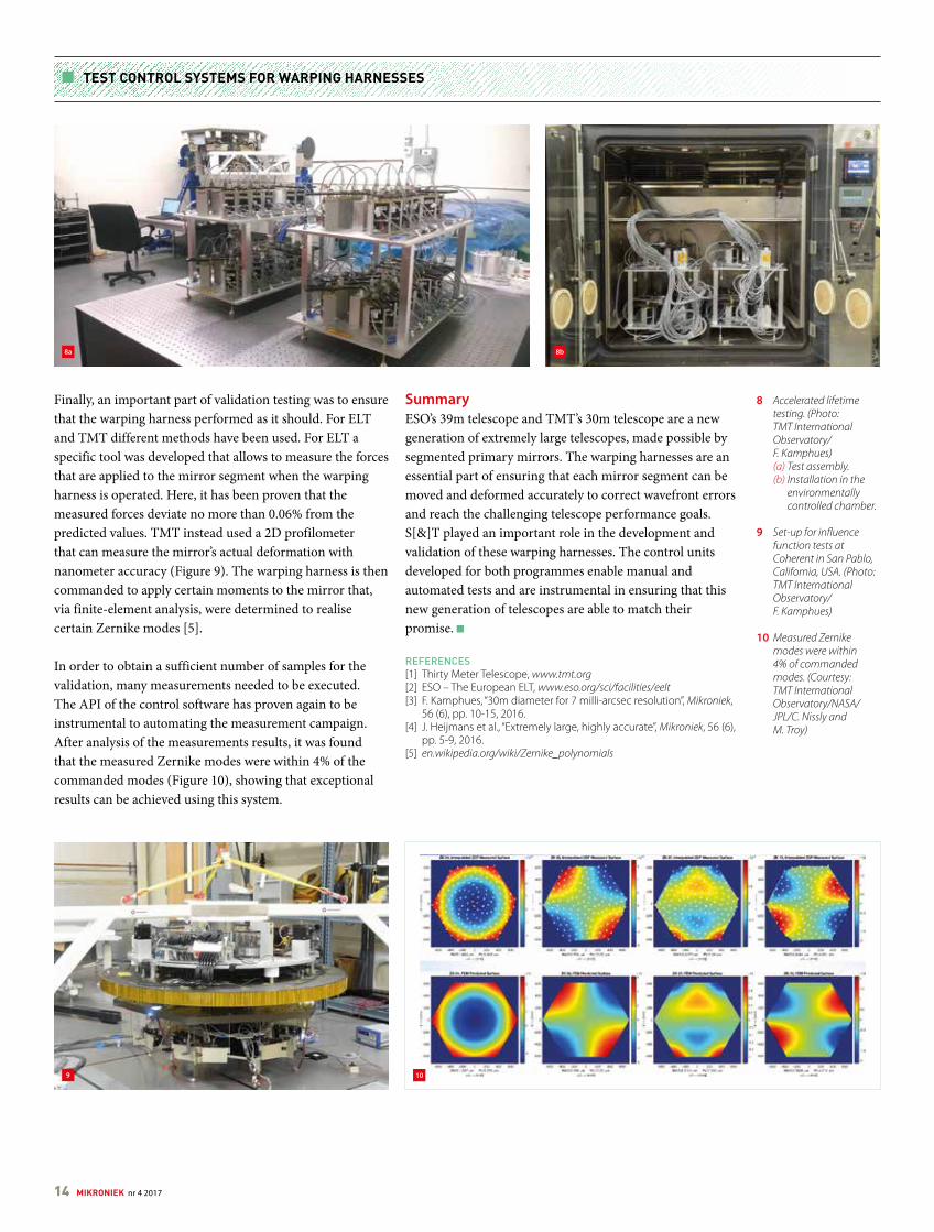
Each control system is equipped with a Linux-based computer that has the software library installed. Automated tests running on this computer (or remotely via a network interface) can directly control the warping harness via the exposed API. In addition, a GUI was developed that uses the same API and allows a test engineer to control the warping harness intuitively (Figure 5).
4 Leaf springs are used to apply a moment to the whiffletree, resulting in forces transferred to the mirror surface, which consequently deforms in a predictable way.
(a) The TMT design. (Courtesy: TMT International Observatory)
(b) ELT uses a slightly different configuration of leaf springs and actuators to apply the moments to the whiffletree. (Courtesy: TNO)
4a 4b
12 MIKRONIEK nr 4 2017
While there are many conceptual similarities between the TMT and ESO ELT programmes, the requirements were not the same. By making the software modular, S[&]T was able to help both projects gain from previous experience and accommodate both challenging and changing hardware systems. Functionality core to each different control system can be expanded by programme-specific modules that easily plug into the Python library. The GUIs were developed with basic building blocks, which allowed efficient development of a GUI tailored to the wishes of the respective programmes.
The signal amplifiers, motion controllers, Linux-based computers, and power supplies are mounted in a custom frame that fits inside a flight case for easy transport (Figure 6). All connections with the warping harness are via easily accessible connectors on the front.
Validation testsBecause the warping harnesses are so essential to the success of the overall telescope performance, they are subjected to exhaustive testing. The controllers developed by S[&]T were instrumental in a rewarding set of test campaigns.
In order to achieve the challenging performance levels, high-risk aspects of the warping harness design have been extensively prototyped and tested. Results of early breadboard tests were used to improve the design and validate the performance of the warping harness before building the first engineering model. These breadboard tests were enabled by the controller’s GUI and API, which allowed rapid iterations in the design cycle.
Functional tests were performed during the assembly phase of the engineering and qualification models. These tests verified that all electrical and mechanical connections are correct and that the control loops are parameterised according to given performance requirements. The controllers’ GUI was very useful in these tests; allowing easy interaction with the system during and after the assembly process, as well as quick iterations of small functional tests (Figure 7).
To ensure reliability of the design, a batch of both the TMT and ELT warping harness units have been subjected to accelerated lifetime testing, during which the warping harness components were put through a lifetime of operational cycles in a short time. By performing accelerated thermal/humidity cycling and operational cycles of the actuators, the warping harness was tested for thermal stresses and wear in order to validate the reliability of the system.
Actuators, leaf springs, and strain gauges were mounted on a smaller assembly for testing that can be installed in an environmentally controlled chamber (Figure 8). During these tests, the API of the control software supported automated tests, developed to push the actuators through the operational cycles, synchronise these cycles with the temperature cycles of the chamber, and record measurement data automatically.
5 The graphical user interface allows a test engineer to intuitively control the warping harness. (Courtesy: S[&]T)
6 The control system fits inside a flight case for easy transport. (Photo: S[&]T/L. Visser)
7 Functional testing at TMT facilities in Pasadena, California, USA. (Photo: TMT International Observatory/ F. Kamphues)
5
6 7
nr 4 2017 MIKRONIEK 13
TEST CONTROL SYSTEMS FOR WARPING HARNESSES
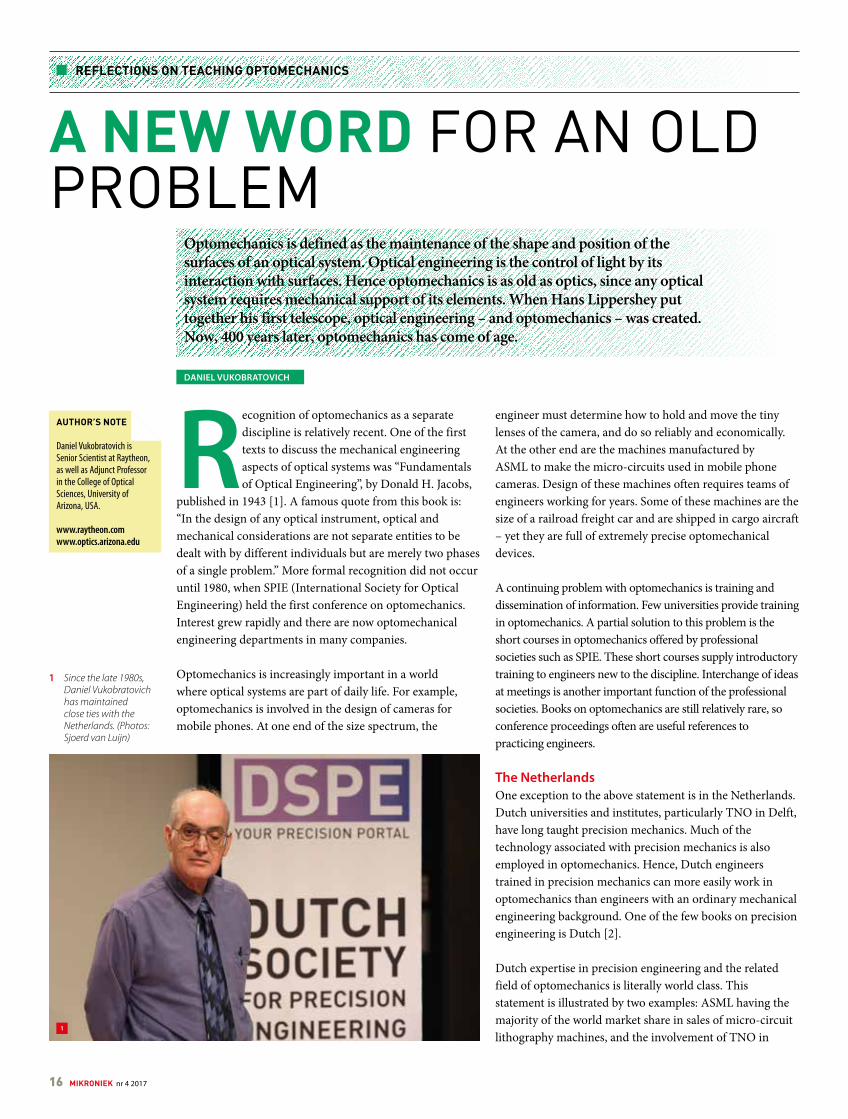
Finally, an important part of validation testing was to ensure that the warping harness performed as it should. For ELT and TMT different methods have been used. For ELT a specific tool was developed that allows to measure the forces that are applied to the mirror segment when the warping harness is operated. Here, it has been proven that the measured forces deviate no more than 0.06% from the predicted values. TMT instead used a 2D profilometer that can measure the mirror’s actual deformation with nanometer accuracy (Figure 9). The warping harness is then commanded to apply certain moments to the mirror that, via finite-element analysis, were determined to realise certain Zernike modes [5].
In order to obtain a sufficient number of samples for the validation, many measurements needed to be executed. The API of the control software has proven again to be instrumental to automating the measurement campaign. After analysis of the measurements results, it was found that the measured Zernike modes were within 4% of the commanded modes (Figure 10), showing that exceptional results can be achieved using this system.
SummaryESO’s 39m telescope and TMT’s 30m telescope are a new generation of extremely large telescopes, made possible by segmented primary mirrors. The warping harnesses are an essential part of ensuring that each mirror segment can be moved and deformed accurately to correct wavefront errors and reach the challenging telescope performance goals. S[&]T played an important role in the development and validation of these warping harnesses. The control units developed for both programmes enable manual and automated tests and are instrumental in ensuring that this new generation of telescopes are able to match their promise.
REFERENCES[1] Thirty Meter Telescope, www.tmt.org[2] ESO – The European ELT, www.eso.org/sci/facilities/eelt[3] F. Kamphues, “30m diameter for 7 milli-arcsec resolution”, Mikroniek,
56 (6), pp. 10-15, 2016.[4] J. Heijmans et al., “Extremely large, highly accurate”, Mikroniek, 56 (6),
pp. 5-9, 2016.[5] en.wikipedia.org/wiki/Zernike_polynomials
8 Accelerated lifetime testing. (Photo: TMT International Observatory/ F. Kamphues)
(a) Test assembly. (b) Installation in the
environmentally controlled chamber.
9 Set-up for influence function tests at Coherent in San Pablo, California, USA. (Photo: TMT International Observatory/ F. Kamphues)
10 Measured Zernike modes were within 4% of commanded modes. (Courtesy: TMT International Observatory/NASA/JPL/C. Nissly and M. Troy)
8a 8b
9 10
14 MIKRONIEK nr 4 2017

#
develop with maxon.
Combining our engineers’ knowhow and ingenuity with the experience build up in more than 50 years in application areas such as operating rooms, semiconductor industryservice robots and even outer space, we develop together with our customers high
Turning ideas into solutions
withmaxon
Open application for academics (MSc and PhD)
- Authoritative knowledge institute in
the field of measurement and calibration
- Interface between between science
and commercial markets
- Varied (international) projects
For a more detailed description visit www.vsl.nl
EH2009
nr 4 2017 MIKRONIEK 15
REFLECTIONS ON TEACHING OPTOMECHANICS
A NEW WORD FOR AN OLD PROBLEM
Optomechanics is defined as the maintenance of the shape and position of the surfaces of an optical system. Optical engineering is the control of light by its interaction with surfaces. Hence optomechanics is as old as optics, since any optical system requires mechanical support of its elements. When Hans Lippershey put together his first telescope, optical engineering – and optomechanics – was created. Now, 400 years later, optomechanics has come of age.
Recognition of optomechanics as a separate discipline is relatively recent. One of the first texts to discuss the mechanical engineering aspects of optical systems was “Fundamentals of Optical Engineering”, by Donald H. Jacobs,
published in 1943 [1]. A famous quote from this book is: “In the design of any optical instrument, optical and mechanical considerations are not separate entities to be dealt with by different individuals but are merely two phases of a single problem.” More formal recognition did not occur until 1980, when SPIE (International Society for Optical Engineering) held the first conference on optomechanics. Interest grew rapidly and there are now optomechanical engineering departments in many companies.
Optomechanics is increasingly important in a world where optical systems are part of daily life. For example, optomechanics is involved in the design of cameras for mobile phones. At one end of the size spectrum, the
DANIEL VUKOBRATOVICH
AUTHOR’S NOTE
Daniel Vukobratovich is Senior Scientist at Raytheon, as well as Adjunct Professor in the College of Optical Sciences, University of Arizona, USA.
www.raytheon.comwww.optics.arizona.edu
engineer must determine how to hold and move the tiny lenses of the camera, and do so reliably and economically. At the other end are the machines manufactured by ASML to make the micro-circuits used in mobile phone cameras. Design of these machines often requires teams of engineers working for years. Some of these machines are the size of a railroad freight car and are shipped in cargo aircraft – yet they are full of extremely precise optomechanical devices.
A continuing problem with optomechanics is training and dissemination of information. Few universities provide training in optomechanics. A partial solution to this problem is the short courses in optomechanics offered by professional societies such as SPIE. These short courses supply introductory training to engineers new to the discipline. Interchange of ideas at meetings is another important function of the professional societies. Books on optomechanics are still relatively rare, so conference proceedings often are useful references to practicing engineers.
The NetherlandsOne exception to the above statement is in the Netherlands. Dutch universities and institutes, particularly TNO in Delft, have long taught precision mechanics. Much of the technology associated with precision mechanics is also employed in optomechanics. Hence, Dutch engineers trained in precision mechanics can more easily work in optomechanics than engineers with an ordinary mechanical engineering background. One of the few books on precision engineering is Dutch [2].
Dutch expertise in precision engineering and the related field of optomechanics is literally world class. This statement is illustrated by two examples: ASML having the majority of the world market share in sales of micro-circuit lithography machines, and the involvement of TNO in
1 Since the late 1980s, Daniel Vukobratovich has maintained close ties with the Netherlands. (Photos: Sjoerd van Luijn)
1
16 MIKRONIEK nr 4 2017
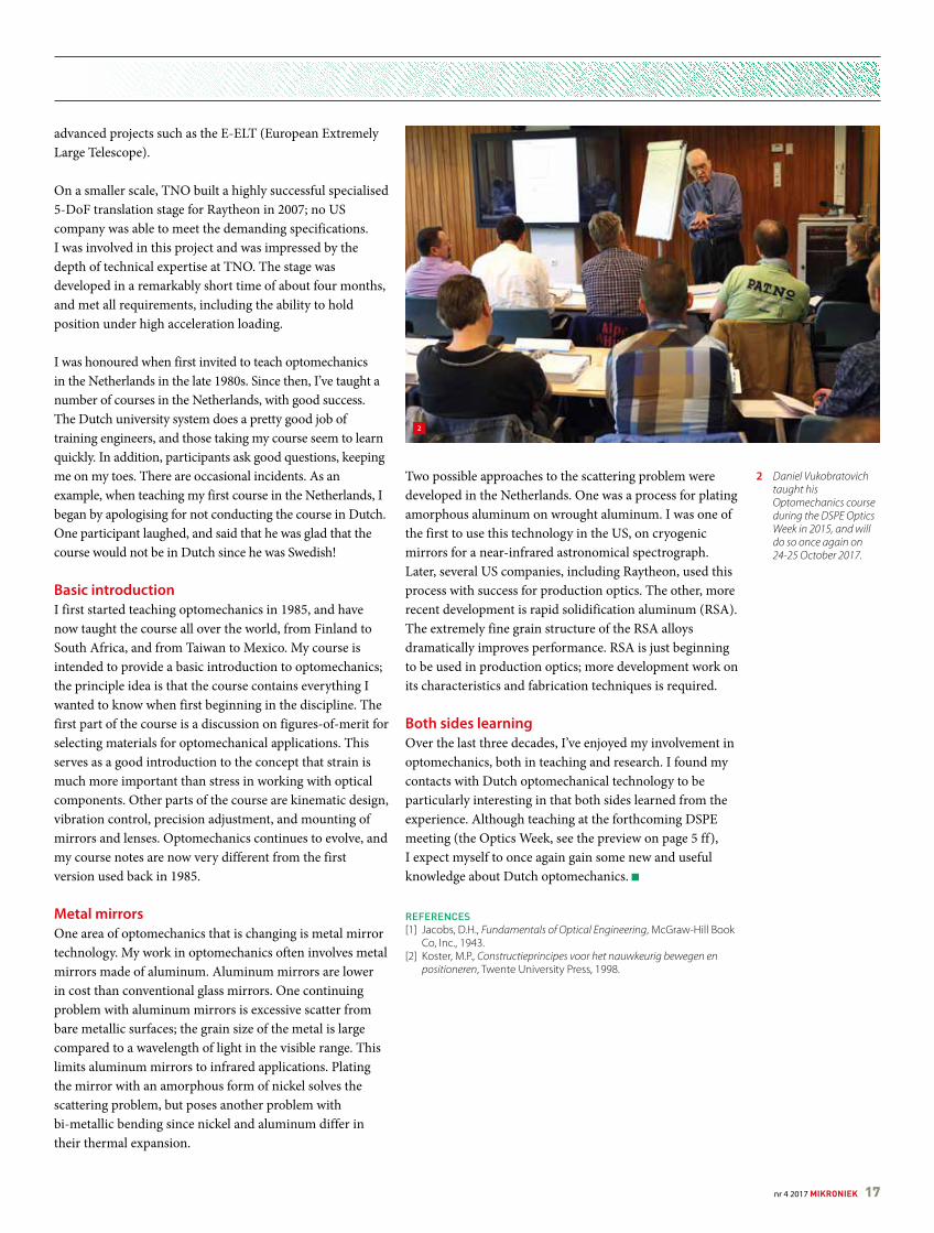
2 Daniel Vukobratovich taught his Optomechanics course during the DSPE Optics Week in 2015, and will do so once again on 24-25 October 2017.
advanced projects such as the E-ELT (European Extremely Large Telescope).
On a smaller scale, TNO built a highly successful specialised 5-DoF translation stage for Raytheon in 2007; no US company was able to meet the demanding specifications. I was involved in this project and was impressed by the depth of technical expertise at TNO. The stage was developed in a remarkably short time of about four months, and met all requirements, including the ability to hold position under high acceleration loading.
I was honoured when first invited to teach optomechanics in the Netherlands in the late 1980s. Since then, I’ve taught a number of courses in the Netherlands, with good success. The Dutch university system does a pretty good job of training engineers, and those taking my course seem to learn quickly. In addition, participants ask good questions, keeping me on my toes. There are occasional incidents. As an example, when teaching my first course in the Netherlands, I began by apologising for not conducting the course in Dutch. One participant laughed, and said that he was glad that the course would not be in Dutch since he was Swedish!
Basic introductionI first started teaching optomechanics in 1985, and have now taught the course all over the world, from Finland to South Africa, and from Taiwan to Mexico. My course is intended to provide a basic introduction to optomechanics; the principle idea is that the course contains everything I wanted to know when first beginning in the discipline. The first part of the course is a discussion on figures-of-merit for selecting materials for optomechanical applications. This serves as a good introduction to the concept that strain is much more important than stress in working with optical components. Other parts of the course are kinematic design, vibration control, precision adjustment, and mounting of mirrors and lenses. Optomechanics continues to evolve, and my course notes are now very different from the first version used back in 1985.
Metal mirrorsOne area of optomechanics that is changing is metal mirror technology. My work in optomechanics often involves metal mirrors made of aluminum. Aluminum mirrors are lower in cost than conventional glass mirrors. One continuing problem with aluminum mirrors is excessive scatter from bare metallic surfaces; the grain size of the metal is large compared to a wavelength of light in the visible range. This limits aluminum mirrors to infrared applications. Plating the mirror with an amorphous form of nickel solves the scattering problem, but poses another problem with bi-metallic bending since nickel and aluminum differ in their thermal expansion.
Two possible approaches to the scattering problem were developed in the Netherlands. One was a process for plating amorphous aluminum on wrought aluminum. I was one of the first to use this technology in the US, on cryogenic mirrors for a near-infrared astronomical spectrograph. Later, several US companies, including Raytheon, used this process with success for production optics. The other, more recent development is rapid solidification aluminum (RSA). The extremely fine grain structure of the RSA alloys dramatically improves performance. RSA is just beginning to be used in production optics; more development work on its characteristics and fabrication techniques is required.
Both sides learningOver the last three decades, I’ve enjoyed my involvement in optomechanics, both in teaching and research. I found my contacts with Dutch optomechanical technology to be particularly interesting in that both sides learned from the experience. Although teaching at the forthcoming DSPE meeting (the Optics Week, see the preview on page 5 ff), I expect myself to once again gain some new and useful knowledge about Dutch optomechanics.
REFERENCES[1] Jacobs, D.H., Fundamentals of Optical Engineering, McGraw-Hill Book
Co, Inc., 1943.[2] Koster, M.P., Constructieprincipes voor het nauwkeurig bewegen en
positioneren, Twente University Press, 1998.
2
nr 4 2017 MIKRONIEK 17
COMPANY PROFILE: OPTICS11
OPTICAL FIBRE INTERFEROMETRY – NEW CONCEPTS AND APPLICATIONS
Optics11 has developed new measurement concepts based on optical fibre interferometry, creating new opportunities in sensing. Combining the benefits of optical fibre sensing with all-optical miniaturised transducers, a first product was launched to perform micromechanical analysis using force sensing in life-science applications. Further exploiting the other advantages of optical fibre sensing, being insensitivity to electrical interference and the ability to bridge long distances, two products are being launched that offer new possibilities in acoustic monitoring and acceleration sensing.
Two powerful technologies can be combined to create new opportunities in measurement applications: optical fibre interferometry and all-optical transducers. Optical fibre interferometry is a technology that
measures the phase of light travelling back from the end of the fibre, providing a fast and precise measurement of any changes in the path length. Interferometry provides the highest bandwidth and the lowest noise floor, and is thus suitable for the most demanding applications. All-optical transducers endow the system with sensitivity for the right parameter, such as force, acoustic vibration or acceleration. By using micro-manufacturing technologies such as optical lithography and laser ablation, very sensitive, miniaturised sensors can be produced, to complement the high-end performance of the interferometer.
Three measurement technologiesOptics11 has developed three different measurement technologies, all based on optical fibre interferometry.
OP1550A single-channel linearised interferometer, able to interrogate a single miniature all-optical sensor. The optical configuration is based on a Fabry-Pérot interferometer (see the box), which projects the interference of two reflections of a laser beam on a photodiode. The first reflection is from a reference surface, which is typically the end face of the fibre. The second reflection is created by the sensitive transducer element, such that a displacement of this element results in a phase difference between the two reflected light beams. A change in the transducer is then
NIEK RIJNVELD
AUTHOR’S NOTE
Niek Rijnveld obtained his Master’s degree in Biomechanical Design at Delft University of Technology, the Netherlands. He worked as a control engineer and a system engineer at TNO and now is the CEO of Optics11, based in Amsterdam, the Netherlands.Optics11 was founded in 2011 as a spin-off company from the Vrije Universiteit Amsterdam. In the six years of its existence, Optics11 has grown from two founders to a team of more than 20 people.
seen as a sinusoidal signal on the photodiode. A high frequency wavelength modulation enables the real-time linearisation of the signal. The main application is in nanoindentation of soft materials.
DeltaSensThis measurement technology can interrogate up to 30 Fabry-Pérot-type sensors in an optical fibre network, connected through standard optical splitters. This interferometer is formed by a broadband light source and a spectrometer. All the Fabry-Pérot interferometric cavities result in a specific footprint on the spectrometer. An advanced algorithm is applied to the data to separate the different cavities in the fibre network and to extract linear signals from each sensor, resulting in a noise floor at the picometer level. The distances between each sensor and to the read-out can be kilometers. The main application is acceleration sensing for condition monitoring.
ZonaSensThis measurement technology offers a completely new sensor configuration: multiple zones in the optical fibre, with lengths of centimeters to meters, can be defined to become extremely sensitive to strain. The beginning and end of a sensing zone are each defined by a so-called Fibre Bragg Grating. This is a local modification in the optical fibre that provides a reflection of just a single laser wavelength. To create an interferometry signal between two of these gratings, a combination of Michelson interferometers is employed. A Michelson interferometer uses just a single reflection on the transducer side that interferes with a reflection in a reference path. Two
18 MIKRONIEK nr 4 2017
linearised Michelson interferometers together form a sensing zone, resulting in a very high sensitivity and a measurement speed of one million samples per second. The first applications are underwater acoustic monitoring and structural health monitoring.
All three measurement technologies have found applications in a broad range of markets, which are described below.
Life-science applicationsIn the field of tissue engineering and regenerative medicine, one of the main goals is to generate tissues and materials that mimic native human tissue properties, in order to restore patient functionality or to perform large-scale treatment testing. In the last few years it has come to light that the micromechanical properties of the cells, tissues and even their physical environments are critical in the success of the application. Academic and industrial researchers are interested in measuring the properties of their samples at the microscale, preferably in physiological conditions, such as in a hydrated state. This is a challenge, since the forces are extremely small and the samples can be very irregular.
The combination of fibre interferometry and all-optical probes provides a unique solution for this challenge: on the one side, interferometry provides the sensitivity to measure forces as low as piconewtons. On the other side, the all-optical miniaturised sensing probes allow full immersion in
FabryPérot interferometry
A change in distance Δx between surfaces R1 and R2 results in a phase difference of Δφ between the two respective reflections (Figure 1). It appears as a sinusoidal pattern (I) on a photodiode. To obtain a linear sensitivity, a cosine signal (Q) is generated using highfrequency modulation of the laser wavelength λ. After normalisation, the linear phase change Δφ can be calculated using Δφ = arctan(I/Q), which subsequently can be unwrapped and scaled to make Δx. 1 Schematic illustration
of Fabry-Pérot interferometry; see text for further explanation.
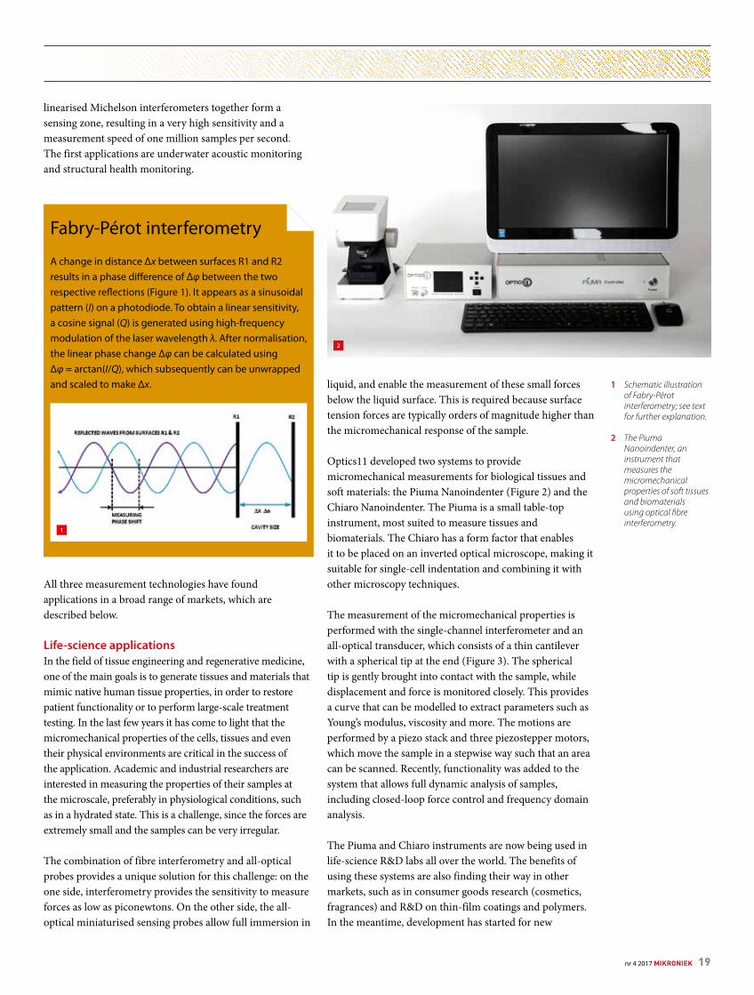
2 The Piuma Nanoindenter, an instrument that measures the micromechanical properties of soft tissues and biomaterials using optical fibre interferometry.
liquid, and enable the measurement of these small forces below the liquid surface. This is required because surface tension forces are typically orders of magnitude higher than the micromechanical response of the sample.
Optics11 developed two systems to provide micromechanical measurements for biological tissues and soft materials: the Piuma Nanoindenter (Figure 2) and the Chiaro Nanoindenter. The Piuma is a small table-top instrument, most suited to measure tissues and biomaterials. The Chiaro has a form factor that enables it to be placed on an inverted optical microscope, making it suitable for single-cell indentation and combining it with other microscopy techniques.
The measurement of the micromechanical properties is performed with the single-channel interferometer and an all-optical transducer, which consists of a thin cantilever with a spherical tip at the end (Figure 3). The spherical tip is gently brought into contact with the sample, while displacement and force is monitored closely. This provides a curve that can be modelled to extract parameters such as Young’s modulus, viscosity and more. The motions are performed by a piezo stack and three piezostepper motors, which move the sample in a stepwise way such that an area can be scanned. Recently, functionality was added to the system that allows full dynamic analysis of samples, including closed-loop force control and frequency domain analysis.
The Piuma and Chiaro instruments are now being used in life-science R&D labs all over the world. The benefits of using these systems are also finding their way in other markets, such as in consumer goods research (cosmetics, fragrances) and R&D on thin-film coatings and polymers. In the meantime, development has started for new
2
1
nr 4 2017 MIKRONIEK 19
COMPANY PROFILE: OPTICS11
technological directions. The all-optical probes also provide possibilities to perform very local electrical, optical and chemical characterisation of samples and single cells. In addition, Optics11 is exploring the added value of a high-throughput version of the Piuma Nanoindenter, to be applied in pharmaceutical research.
Remote sensingThe benefits of optical fibre sensing are well known: insensitivity to electrical and magnetic fields, performance in challenging environments such as in liquids or high temperature, and the ability to cover distances of kilometers without significant signal loss. Many successful technologies are exploiting these benefits by providing for example temperature, pressure or strain measurement systems for challenging industries. However, the current solutions are typically limited in sensitivity and bandwidth, which keep many applications out of reach for optical fibre sensing. The DeltaSens and ZonaSens technologies can step into this gap, providing solutions for all-optical acceleration sensing and high-frequency acoustic monitoring. Acceleration sensing and acoustic monitoring is important in applications such as structural health monitoring of wind turbines, airplanes
and infrastructure, in detection and mapping with sonar and seismology, and in active monitoring of processes in oil and gas.
Acceleration sensingOne limitation in currently available optical fibre sensing systems is the transducer sensitivity, which is most apparent in acceleration sensing: even though the optical measurement principle is often very sensitive to changes, the operating principle still requires elongation of the optical fibre in order to provide an acceleration signal. DeltaSens can overcome this problem by using Fabry-Pérot interferometry. This sensing principle relies on the combination of a reflection of the end face of the optical fibre, and a reflection of a free second surface. This provides complete freedom to create a miniaturised transducer that can sense changes without elongating the fibre.
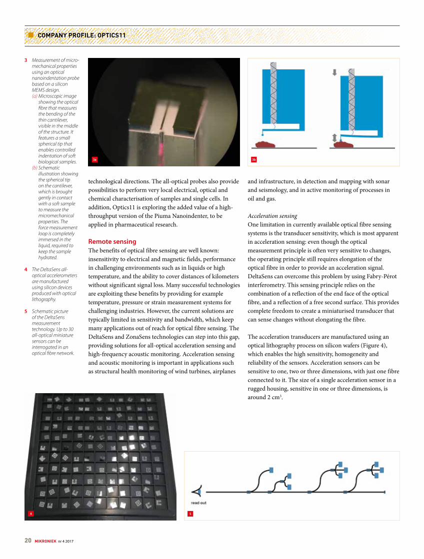
The acceleration transducers are manufactured using an optical lithography process on silicon wafers (Figure 4), which enables the high sensitivity, homogeneity and reliability of the sensors. Acceleration sensors can be sensitive to one, two or three dimensions, with just one fibre connected to it. The size of a single acceleration sensor in a rugged housing, sensitive in one or three dimensions, is around 2 cm3.
4
3 Measurement of micro-mechanical properties using an optical nanoindentation probe based on a silicon MEMS design.
(a) Microscopic image showing the optical fibre that measures the bending of the thin cantilever, visible in the middle of the structure. It features a small spherical tip that enables controlled indentation of soft biological samples.
(b) Schematic illustration showing the spherical tip on the cantilever, which is brought gently in contact with a soft sample to measure the micromechanical properties. The force measurement loop is completely immersed in the liquid, required to keep the sample hydrated.
4 The DeltaSens all-optical accelerometers are manufactured using silicon devices produced with optical lithography.
5 Schematic picture of the DeltaSens measurement technology. Up to 30 all-optical miniature sensors can be interrogated in an optical fibre network.
3b3a
5
20 MIKRONIEK nr 4 2017
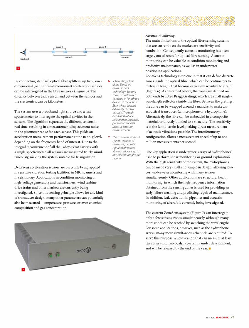
By connecting standard optical fibre splitters, up to 30 one-dimensional (or 10 three-dimensional) acceleration sensors can be interrogated in the fibre network (Figure 5). The distance between each sensor, and between the sensors and the electronics, can be kilometers.
The system uses a broadband light source and a fast spectro meter to interrogate the optical cavities in the sensors. The algorithm separates the different sensors in real time, resulting in a measurement displacement noise in the picometer range for each sensor. This yields an acceleration measurement performance at the nano-g level, depending on the frequency band of interest. Due to the integral measurement of all the Fabry-Pérot cavities with a single spectrometer, all sensors are measured truely simul-taneously, making the system suitable for triangulation.
DeltaSens acceleration sensors are currently being applied in sensitive vibration testing facilities, in MRI scanners and in seismology. Applications in condition monitoring of high-voltage generators and transformers, wind turbine drive trains and other markets are currently being investigated. Since this sensing principle allows for any kind of transducer design, many other parameters can potentially also be measured – temperature, pressure, or even chemical composition and gas concentration.
Acoustic monitoringThe main limitations of the optical fibre sensing systems that are currently on the market are sensitivity and bandwidth. Consequently, acoustic monitoring has been largely out of reach for optical fibre sensing. Acoustic monitoring can be valuable in condition monitoring and predictive maintenance, as well as in underwater positioning applications.ZonaSens technology is unique in that it can define discrete zones inside the optical fibre, which can be centimeters to meters in length, that become extremely sensitive to strain (Figure 6). As described before, the zones are defined on both ends by Fibre Bragg Gratings, which are small single-wavelength reflectors inside the fibre. Between the gratings, the zone can be wrapped around a mandrel to make an acoustical transducer (a microphone or a hydrophone). Alternatively, the fibre can be embedded in a composite material, or directly bonded to a structure. The sensitivity is at the femto-strain level, making direct measurement of acoustic vibrations possible. The interferometry configuration allows a measurement speed of up to one million measurements per second.
One key application is underwater: arrays of hydrophones used to perform sonar monitoring or ground exploration. With the high sensitivity of the system, the hydrophones can be made very small and simple in design, allowing low-cost underwater monitoring with many sensors simultaneously. Other applications are structural health monitoring, in which the high-frequency information obtained from the sensing zones is used for providing an early failure warning and predicting required maintenance. In addition, leak detection in pipelines and acoustic monitoring of aircraft is currently being investigated.
The current ZonaSens system (Figure 7) can interrogate only a few sensing zones simultaneously, although many more zones can be reached by switching the wavelengths. For some applications, however, such as the hydrophone arrays, many more simultaneous channels are required. To serve this purpose, a new version that can measure at least ten zones simultaneously is currently under development, and will be released by the end of the year.
6
6 Schematic picture of the ZonaSens measurement technology. Sensing zones of centimeters to meters in length are defined in the optical fibre, which become extremely sensitive to strain. The high bandwidth of one million measurements per second enables acoustic emission measurements.
7 The ZonaSens read-out system, capable of measuring acoustic signals with optical fibre transducers, up to one million samples per second.
7
nr 4 2017 MIKRONIEK 21

Ready to get started?Developing, creating, assembling and testing com-
plex (opto)mechatronic systems and mechanical
modules is just like taking part in a regatta. Everything
revolves around precision and maneuverability, NTS
knows that better than anyone. We have gathered a lot
of knowledge and know-how of systems and modules
for handling, transfer and positioning in machines. We
apply our knowledge and competences in various
fields worldwide to our clients’ unique products: high-
tech machine builders (OEMs).
In this way, they can focus on their core processes and
also deliver machines with a shorter lead time, at
lower costs. Our line pattern is flexible and ambitious
and ensures that systems remain on track, throug-
hout the entire lifecycle. We navigate, tack and defy the
wind. Fast and good. This is the way we help our clients
to catch the wind, so that they can accelerate in their
business pursuits. Would you also like to tack with
NTS? We would be delighted to throw a line out for
further acquaintance.
www.nts-group.nl
Accelerating your business
22 MIKRONIEK nr 4 2017
NEW OPPORTUNITIES FOR NANOMEFOS FREEFORM OPTICS MEASUREMENT MACHINE
EXPORTING DUTCH OPTOMECHATRONICS TO CHINA
NANOMEFOS was developed in the Netherlands ten years ago and today it still represents the state of the art in measuring the absolute form of aspherical and freeform optical surfaces. For years its cost price prohibited commercialisation, but recent interest from China has paved the way for Nanomefos 2.0. The updated measurement machine will be constructed and marketed by a new joint venture, DUI (Dutch United Instruments). The primary focus is on reducing cost price and enabling the embedding of the measurement procedure in the corrective polishing process.
The Nanomefos (Nanometer Accuracy Non-contact Measurement of Freeform Optical Surfaces) measurement machine [1] was developed in the previous decade by TNO, Eindhoven University of Technology (TU/e)
and VSL, the Dutch national metrology institute. As part of the project, a proof-of-principle machine was built and has subsequently been operated by TNO. Nanomefos was ahead of its time, due to its ingenious mechatronic design, including a metrology frame (Figure 1), and still today represents the state of the art in measuring the absolute form of aspherical and freeform optical surfaces.
Nanomefos 1.0Applying aspherical (non-rotationally symmetrical) and freeform optics has many advantages for high-end optical systems in lithography, space, astronomy and other applications. In combination with diamond turning and
corrective polishing, Nanomefos enables the fabrication of complex and large optical surfaces (mirrors as well as lenses) with nanometer-level accuracy. Up until now, TNO has been the only provider of this high-end service using Nanomefos.
Properties of the original Nanomefos machine include [2]:• Universal measurement of aspherical and freeform optical
surfaces.• Measurement volume of Ø500 mm x 100 mm.• Convex and concave, up to 45°.• Non-contact.• Measurement uncertainty < 15 nm rms.• Fast (minutes for > 500k points).
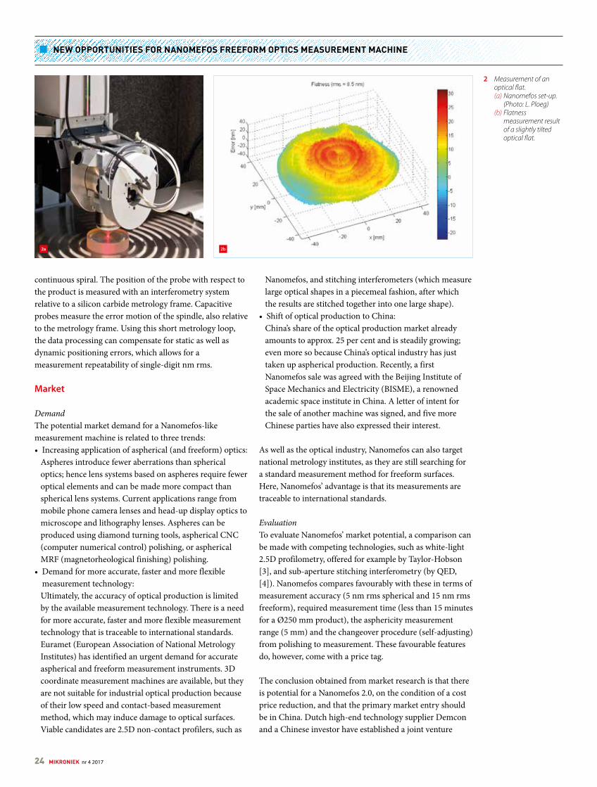
The optical surface to be measured (‘the product’) is placed on a continuously rotating air-bearing spindle, while a specially developed optical probe scans over it at high speed (up to 1.5 m/s). The probe is positioned over the product using an air-bearing motion system and its measurement is based on the differential confocal method, which measures how well a surface is in focus. When a surface moves through focus, the response is an S-curve with a zero-crossing at best focus and a few μm of near-linear response around it. Figure 2 shows the measurement set-up and an illustrative result.
The departure from rotation symmetry of the surface that lies within the measurement range of the probe, amounts to 5 mm. The trajectory for which the height profile of the surface is measured, consists of circular tracks or a
1 Schematic Nanomefos machine concept. [1]
1
nr 4 2017 MIKRONIEK 23
NEW OPPORTUNITIES FOR NANOMEFOS FREEFORM OPTICS MEASUREMENT MACHINE
continuous spiral. The position of the probe with respect to the product is measured with an interferometry system relative to a silicon carbide metrology frame. Capacitive probes measure the error motion of the spindle, also relative to the metrology frame. Using this short metrology loop, the data processing can compensate for static as well as dynamic positioning errors, which allows for a measurement repeatability of single-digit nm rms.
Market
DemandThe potential market demand for a Nanomefos-like measurement machine is related to three trends:• Increasing application of aspherical (and freeform) optics: Aspheres introduce fewer aberrations than spherical
optics; hence lens systems based on aspheres require fewer optical elements and can be made more compact than spherical lens systems. Current applications range from mobile phone camera lenses and head-up display optics to microscope and lithography lenses. Aspheres can be produced using diamond turning tools, aspherical CNC (computer numerical control) polishing, or aspherical MRF (magnetorheological finishing) polishing.
• Demand for more accurate, faster and more flexible measurement technology:
Ultimately, the accuracy of optical production is limited by the available measurement technology. There is a need for more accurate, faster and more flexible measurement technology that is traceable to international standards. Euramet (European Association of National Metrology Institutes) has identified an urgent demand for accurate aspherical and freeform measurement instruments. 3D coordinate measurement machines are available, but they are not suitable for industrial optical production because of their low speed and contact-based measurement method, which may induce damage to optical surfaces. Viable candidates are 2.5D non-contact profilers, such as
Nanomefos, and stitching interferometers (which measure large optical shapes in a piecemeal fashion, after which the results are stitched together into one large shape).
• Shift of optical production to China: China’s share of the optical production market already
amounts to approx. 25 per cent and is steadily growing; even more so because China’s optical industry has just taken up aspherical production. Recently, a first Nanomefos sale was agreed with the Beijing Institute of Space Mechanics and Electricity (BISME), a renowned academic space institute in China. A letter of intent for the sale of another machine was signed, and five more Chinese parties have also expressed their interest.
As well as the optical industry, Nanomefos can also target national metrology institutes, as they are still searching for a standard measurement method for freeform surfaces. Here, Nanomefos’ advantage is that its measurements are traceable to international standards.
EvaluationTo evaluate Nanomefos’ market potential, a comparison can be made with competing technologies, such as white-light 2.5D profilometry, offered for example by Taylor-Hobson [3], and sub-aperture stitching interferometry (by QED, [4]). Nanomefos compares favourably with these in terms of measurement accuracy (5 nm rms spherical and 15 nm rms freeform), required measurement time (less than 15 minutes for a Ø250 mm product), the asphericity measurement range (5 mm) and the changeover procedure (self-adjusting) from polishing to measurement. These favourable features do, however, come with a price tag.
The conclusion obtained from market research is that there is potential for a Nanomefos 2.0, on the condition of a cost price reduction, and that the primary market entry should be in China. Dutch high-end technology supplier Demcon and a Chinese investor have established a joint venture
2 Measurement of an optical flat.
(a) Nanomefos set-up. (Photo: L. Ploeg)
(b) Flatness measurement result of a slightly tilted optical flat.
2a 2b
24 MIKRONIEK nr 4 2017
named DUI (for both ‘Dutch United Instruments’ and ‘dui’, which in Mandarin Chinese can mean correct, right) for the construction and marketing of the machines. Sales and service will be performed through a strategic cooperation with FUMA, a sales and service agency in China. Collaborations with agencies in other countries will be established as well.
Update and redesignFor a quick market entry, there is no time for a complete redesign, so the first action will be to give the current proof-of-principle machine (Figure 3) an update, yielding the so-called Nanomefos 500. Production drawings have to be derived from the available 3D CAD model, the bill of materials has to be checked against current availability of parts and the target for cost price reduction is 20-30 per cent. The functionality will be adapted to enable the embedding of the measurement procedure in the corrective polishing process.
The wish list for a more extensive redesign, resulting in the Nanomefos 2.0 platform, includes extending the asphericity measurement range beyond 5 mm, to enable the measurement of larger products (up to Ø500 mm) and making amendments to the optical probe to allow the measurement of surfaces with higher roughness values. When the acceptable Ra can be increased from the current 10-20 nm to 50 nm, the measurement procedure can start earlier in the production process, which may shorten total throughput time. Lessons learned from the Nanomefos+ update will be incorporated into the redesign. The ultimate goal is to design a platform from which several versions can be derived for smaller and larger products with corresponding prices and target markets.
Dutch undertakingThe construction and redesign of Nanomefos, including the development of more extensive, user-friendly analytics software, will be carried out by Demcon advanced mechatronics and Demcon Focal optomechatronic systems in cooperation with the Dutch optomechatronic industry. “We want to place a flag for Dutch optomechatronics and are very much indebted to the godfathers of Nanomefos: TNO, TU/e and VSL”, says Gerard van den Eijkel, business unit manager at Demcon Focal optomechatronic systems.
“We will collaborate with organisations such as TNO, as a knowledge provider, and the Dutch Optics Centre, recently established by TNO and Delft University of Technology. To bring forward the Nanomefos instruments, we will of course leverage the strong Dutch (opto)mechatronic industry including companies such as VDL, NTS, Hittech, IBS and Tecnotion. We will also try to involve the inventors who were engaged in the realisation of the original Nanomefos, such as Rens Henselmans, Lennino Cacace, Wim van Amstel and Pieter Kappelhof. We all felt it was a shame that this ‘highlight of Dutch optomechatronics’ could not be commercialised yet. Now the time has come.”
REFERENCES[1] R. Henselmans, “Design, Realization and Testing of NANOMEFOS”,
Mikroniek 48 (6), pp. 5-8, 2008.[2] www.tno.nl/nanomefos[3] www.taylor-hobson.com [4] www.qedmrf.com
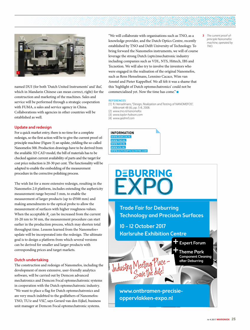
3 The current proof-of-principle Nanomefos machine, operated by TNO.
INFORMATION WWW.DEMCON.NL WWW.TNO.NL WWW.TUE.NL WWW.VSL.NL WWW.DUTCHOPTICSCENTRE.COM
3
Trade Fair for Deburring Technology and Precision Surfaces
10 – 12 October 2017 Karlsruhe Exhibition Centre
www.ontbramen-precisie- oppervlakken-expo.nl
++
Expert Forum
Theme ParkComponent Cleaning after Deburring
nr 4 2017 MIKRONIEK 25
SAXION MECHATRONICS FORUM ON MODULAR BUILDING BLOCKS FOR ROBOTIC SYSTEMS
GETTING A GRIP ON MEDICAL AND MODULAR ROBOTICS
The first Saxion Mechatronics Forum, dedicated to medical and modular robotics, featured the results of the RAAK-PRO project ‘Medical Robotics’. This project involved research institutes collaborating with industrial partners to seek innovative solutions for care robotics and medical rehabilitation. The modular character of the project enabled researchers to incorporate their solutions into various platforms. This article highlights the primary results of the project, which can be extended beyond medical applications into industrial automation and agriculture, and also gives an overview of the Mechatronics Forum.
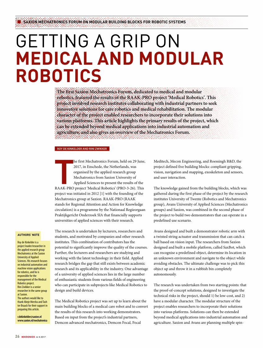
The first Mechatronics Forum, held on 29 June, 2017, in Enschede, the Netherlands, was organised by the applied research group Mechatronics from Saxion University of Applied Sciences to present the results of the
RAAK-PRO project ‘Medical Robotics’ (PRO-3-26). This project was initiated in 2012 [1] with the founding of the Mechatronics group at Saxion. RAAK-PRO (RAAK stands for Regional Attention and Action for Knowledge circulation) is a programme by the Nationaal Regieorgaan Praktijkgericht Onderzoek SIA that financially supports universities of applied sciences with their research.
The research is undertaken by lecturers, researchers and students, and motivated by companies and other research institutes. This combination of contributors has the potential to significantly improve the quality of the courses. Further, the lecturers and researchers are studying and working with the latest technology in their field. Applied research bridges the gap that still exists between academic research and its applicability in the industry. One advantage of a university of applied sciences lies in the large number of enthusiastic students from various fields of engineering who can participate in subprojects like Medical Robotics to design and build devices.
The Medical Robotics project was set up to learn about the main building blocks of a medical care robot and to convert the results of this research into working demonstrators. Based on input from the project’s industrial partners, Demcon advanced mechatronics, Demcon Focal, Focal
ROY DE KINKELDER AND RINI ZWIKKER
AUTHORS’ NOTE
Roy de Kinkelder is a project leader/researcher in the applied research group Mechatronics at the Saxion University of Applied Sciences. His research focuses on industrial automation and machine vision applications for robotics, and he is responsible for the management of the Medical Robotics project. Rini Zwikker is a senior researcher in the same group at Saxion.The authors would like to thank Abeje Mersha and Tash ter Braack for their support in preparing this article.
[email protected]/mechatronica
Meditech, Mecon Engineering, and Roessingh R&D, the project defined five building blocks: compliant gripping, vision, navigation and mapping, exoskeleton and sensors, and user interaction.
The knowledge gained from the building blocks, which was gathered during the first phase of the project by the research institutes University of Twente (Robotics and Mechatronics group), Avans University of Applied Sciences (Mechatronics groups) and Saxion, was combined in the second phase of the project to build two demonstrators that can operate in a predefined use scenario.
Avans designed and built a demonstrator robotic arm with a twisted string actuator and transmission that can catch a ball based on vision input. The researchers from Saxion designed and built a mobile platform, called SaxBot, which can recognise a predefined object, determine its location in an unknown environment and navigate to the object while avoiding obstacles. The ultimate challenge was to pick this object up and throw it in a rubbish bin completely autonomously.
The research was undertaken from two starting points: that the proof-of-concept solutions, designed to investigate the technical risks in the project, should 1) be low-cost, and 2) have a modular character. The modular structure of the project enables researchers to incorporate their solutions into various platforms. Solutions can then be extended beyond medical applications into industrial automation and agriculture. Saxion and Avans are planning multiple spin-
26 MIKRONIEK nr 4 2017
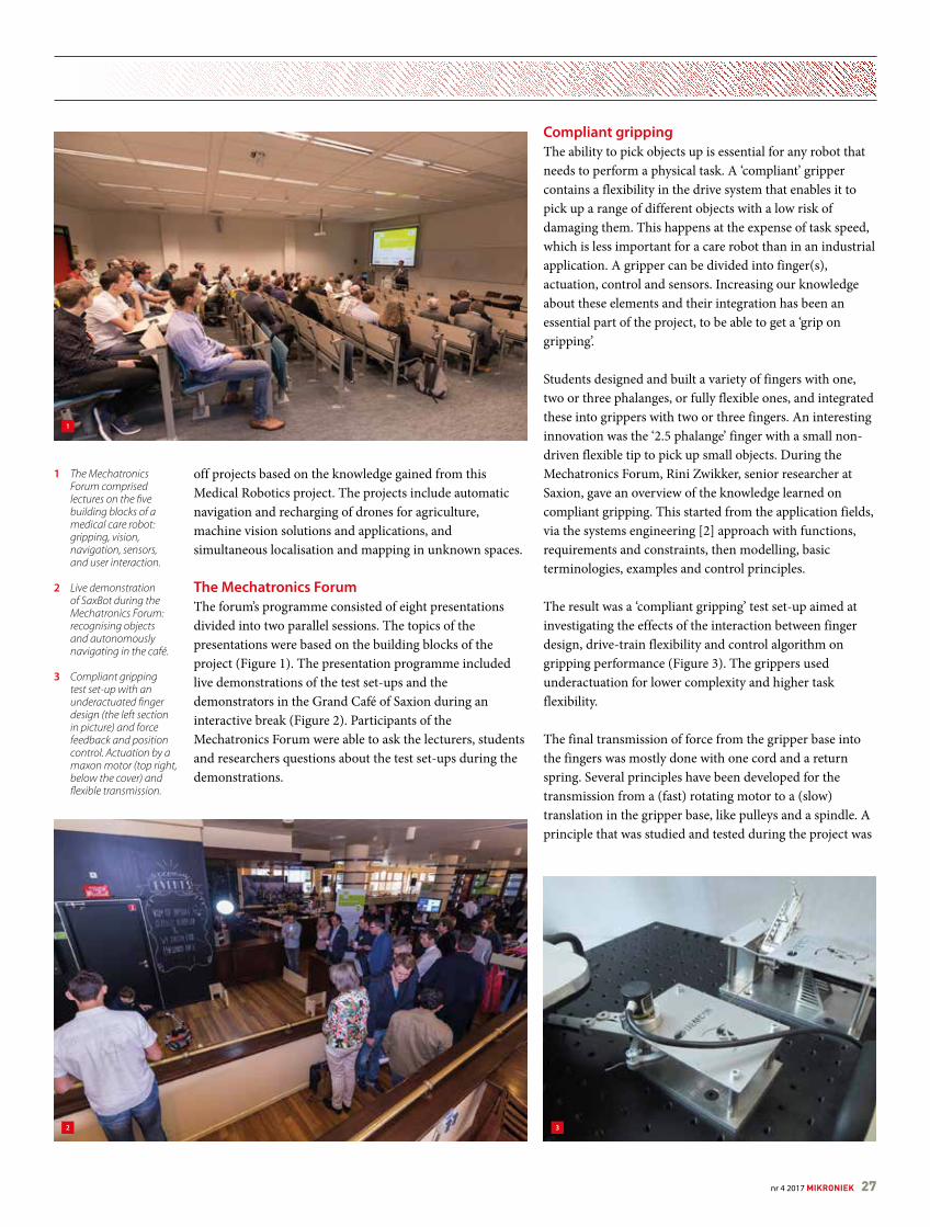
1 The Mechatronics Forum comprised lectures on the five building blocks of a medical care robot: gripping, vision, navigation, sensors, and user interaction.
2 Live demonstration of SaxBot during the Mechatronics Forum: recognising objects and autonomously navigating in the café.
3 Compliant gripping test set-up with an underactuated finger design (the left section in picture) and force feedback and position control. Actuation by a maxon motor (top right, below the cover) and flexible transmission.
off projects based on the knowledge gained from this Medical Robotics project. The projects include automatic navigation and recharging of drones for agriculture, machine vision solutions and applications, and simultaneous localisation and mapping in unknown spaces.
The Mechatronics ForumThe forum’s programme consisted of eight presentations divided into two parallel sessions. The topics of the presentations were based on the building blocks of the project (Figure 1). The presentation programme included live demonstrations of the test set-ups and the demonstrators in the Grand Café of Saxion during an interactive break (Figure 2). Participants of the Mechatronics Forum were able to ask the lecturers, students and researchers questions about the test set-ups during the demonstrations.
Compliant grippingThe ability to pick objects up is essential for any robot that needs to perform a physical task. A ‘compliant’ gripper contains a flexibility in the drive system that enables it to pick up a range of different objects with a low risk of damaging them. This happens at the expense of task speed, which is less important for a care robot than in an industrial application. A gripper can be divided into finger(s), actuation, control and sensors. Increasing our knowledge about these elements and their integration has been an essential part of the project, to be able to get a ‘grip on gripping’.
Students designed and built a variety of fingers with one, two or three phalanges, or fully flexible ones, and integrated these into grippers with two or three fingers. An interesting innovation was the ‘2.5 phalange’ finger with a small non-driven flexible tip to pick up small objects. During the Mechatronics Forum, Rini Zwikker, senior researcher at Saxion, gave an overview of the knowledge learned on compliant gripping. This started from the application fields, via the systems engineering [2] approach with functions, requirements and constraints, then modelling, basic terminologies, examples and control principles.
The result was a ‘compliant gripping’ test set-up aimed at investigating the effects of the interaction between finger design, drive-train flexibility and control algorithm on gripping performance (Figure 3). The grippers used underactuation for lower complexity and higher task flexibility.
The final transmission of force from the gripper base into the fingers was mostly done with one cord and a return spring. Several principles have been developed for the transmission from a (fast) rotating motor to a (slow) translation in the gripper base, like pulleys and a spindle. A principle that was studied and tested during the project was
1
2 3
nr 4 2017 MIKRONIEK 27
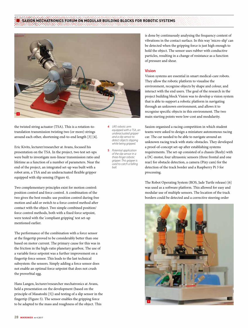
SAXION MECHATRONICS FORUM ON MODULAR BUILDING BLOCKS FOR ROBOTIC SYSTEMS
the twisted string actuator (TSA). This is a rotation-to-translation transmission twisting two (or more) strings around each other, shortening end-to-end length [3] [4].
Eric Kivits, lecturer/researcher at Avans, focused his presentation on the TSA. In the project, two test set-ups were built to investigate non-linear transmission ratio and lifetime as a function of a number of parameters. Near the end of the project, an integrated set-up was built with a robot arm, a TSA and an underactuated flexible gripper equipped with slip sensing (Figure 4).
Two complementary principles exist for motion control: position control and force control. A combination of the two gives the best results: use position control during free motion and add or switch to a force control method after contact with the object. Two simple combined position/force control methods, both with a fixed force setpoint, were tested with the ‘compliant gripping’ test set-up mentioned earlier.
The performance of the combination with a force sensor at the fingertip proved to be considerably better than one based on motor current. The primary cause for this was in the friction in the high-ratio planetary gearbox. The use of a variable force setpoint was a further improvement on a fingertip force sensor. This leads to the last technical subsystem: the sensors. Simply adding a force sensor does not enable an optimal force setpoint that does not crush the proverbial egg.
Hans Langen, lecturer/researcher mechatronics at Avans, held a presentation on the development (based on the principle of Masatoshi [5]) and testing of a slip sensor in the fingertip (Figure 5). The sensor enables the gripping force to be adapted to the mass and roughness of the object. This
is done by continuously analysing the frequency content of vibrations in the contact surface. In this way ‘micro-slip’ can be detected when the gripping force is just high enough to hold the object. The sensor uses rubber with conductive particles, resulting in a change of resistance as a function of pressure and shear.
VisionVision systems are essential in smart medical-care robots. They allow the robotic platform to visualise the environment, recognise objects by shape and colour, and interact with the end users. The goal of the research in the project building block Vision was to develop a vision system that is able to support a robotic platform in navigating through an unknown environment, and allows it to recognise specific objects in this environment. The two main starting points were low-cost and modularity.
Saxion organised a racing competition in which student teams were asked to design a miniature autonomous racing car. The car needed to be able to navigate around an unknown racing track with static obstacles. They developed a proof-of-concept set-up after establishing systems requirements. The set-up consisted of a chassis (Reely) with a DC-motor, four ultrasonic sensors (three frontal and one rear) for obstacle detection, a camera (Pixy cam) for the detection of the track border and a Raspberry Pi 3 for processing.
The Robot Operating System (ROS, Jade Turtle release) [6] was used as a software platform. This allowed for easy and modular use of multiple sensors. The location of the track borders could be detected and a corrective steering order
4 UR5 robotic arm equipped with a TSA, an underactuated gripper and a slip sensor to detect objects slipping while being gripped.
5 Potential application of the slip sensor in a three-finger robotic gripper. This gripper is used to catch a falling ball.
4
5
28 MIKRONIEK nr 4 2017
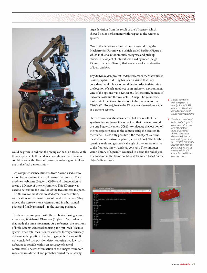
could be given to redirect the racing car back on track. With these experiments the students have shown that vision in combination with ultrasonic sensors can be a good tool for use in the final demonstrator.
Two computer science students from Saxion used stereo vision for navigating in an unknown environment. They used two webcams (Logitech C920) and triangulation to create a 3D map of the environment. This 3D map was used to determine the location of the two cameras in space. The 3D environment was created after lens correction, rectification and determination of the disparity map. They moved the stereo-vision system around in a horizontal plane and finally returned it to the starting position.
The data were compared with those obtained using a more expensive, ROS-based VI-sensor (Skybotix, Switzerland) that made the same movement. As a reference, the positions of both systems were tracked using an OptiTrack (Flex13) system. The OptiTrack uses ten cameras to very accurately determine the position of reflecting objects in a room. It was concluded that position detection using two low-cost webcams is possible within an accuracy of several centimetres. The synchronisation of the images from both webcams was difficult and probably caused the relatively
large deviation from the result of the VI-sensor, which showed better performance with respect to the reference system.
One of the demonstrations that was shown during the Mechatronics Forum was a vehicle called SaxBot (Figure 6), which is able to autonomously recognise and pick up objects. The object of interest was a red cylinder (height 75 mm, diameter 60 mm) that was made of a combination of foam and felt.
Roy de Kinkelder, project leader/researcher mechatronics at Saxion, explained during his talk on vision that they considered multiple vision modules in order to determine the location of such an object in an unknown environment. One of the options was a Kinect 360 (Microsoft), because of its lower costs and the available 3D map. The geometrical footprint of the Kinect turned out to be too large for the X80SV (Dr Robot), hence the Kinect was deemed unusable as a camera system.
Stereo vision was also considered, but as a result of the synchronisation issues it was decided that the team would use one Logitech camera (C920) to calculate the location of the red object relative to the camera using the location in the frame. This is only possible if the red object is always located in one horizontal plane (i.e. on a floor). The height, opening angle and geometrical angle of the camera relative to the floor are known and stay constant. The computer vision library of OpenCV was used to detect the red object. The location in the frame could be determined based on the object’s dimensions.
6 SaxBot comprises a vision system, a manipulator (CLAM arm, Correll Lab) and a modified DrRobot X80SV mobile platform.
7 The detection of a red object in the Logitech camera’s field of view. First the contour (pale blue line) of the red object was determined, then a rectangle (green line) was created. Finally, the location of the centre point (magenta) was calculated. For this example, a red Duplo block was used.
6
7
nr 4 2017 MIKRONIEK 29
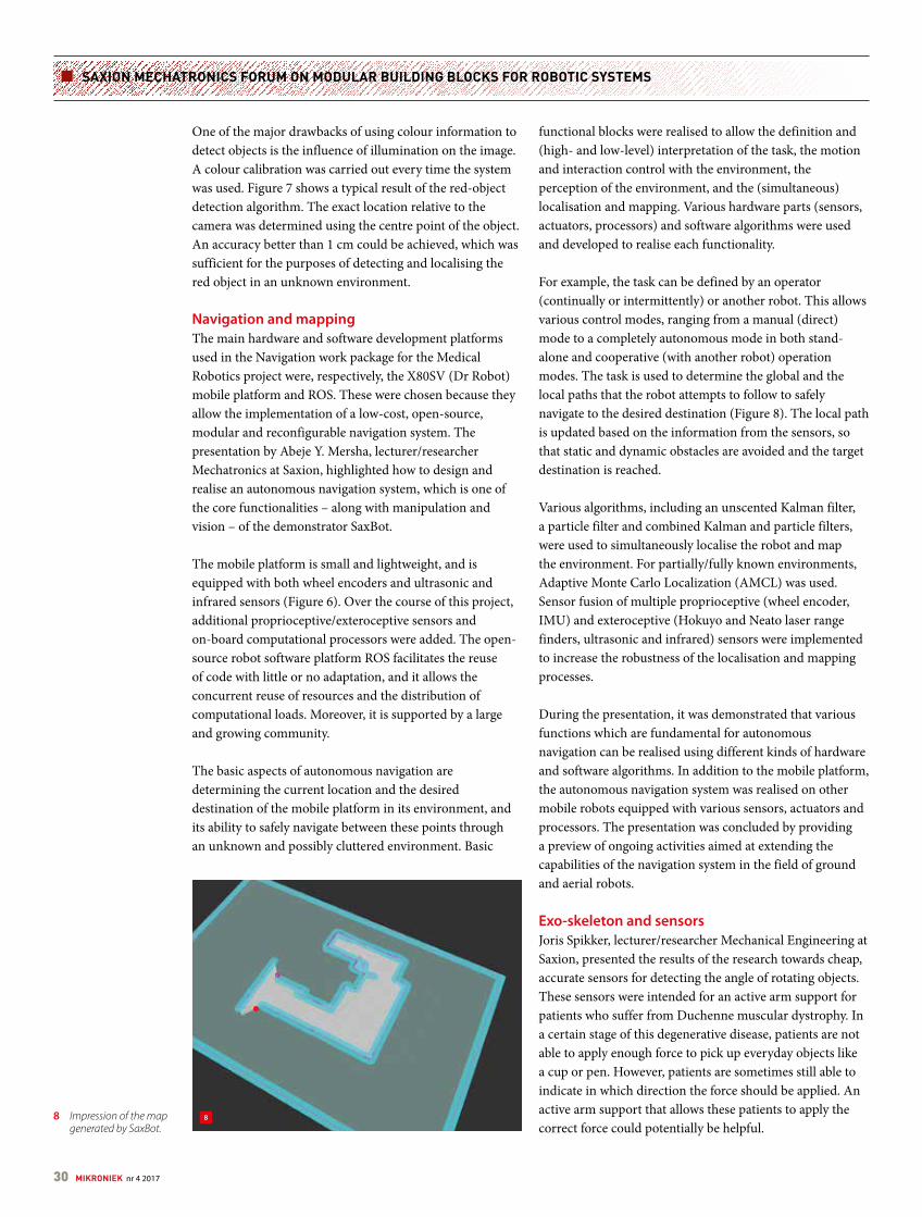
SAXION MECHATRONICS FORUM ON MODULAR BUILDING BLOCKS FOR ROBOTIC SYSTEMS
One of the major drawbacks of using colour information to detect objects is the influence of illumination on the image. A colour calibration was carried out every time the system was used. Figure 7 shows a typical result of the red-object detection algorithm. The exact location relative to the camera was determined using the centre point of the object. An accuracy better than 1 cm could be achieved, which was sufficient for the purposes of detecting and localising the red object in an unknown environment.
Navigation and mappingThe main hardware and software development platforms used in the Navigation work package for the Medical Robotics project were, respectively, the X80SV (Dr Robot) mobile platform and ROS. These were chosen because they allow the implementation of a low-cost, open-source, modular and reconfigurable navigation system. The presentation by Abeje Y. Mersha, lecturer/researcher Mechatronics at Saxion, highlighted how to design and realise an autonomous navigation system, which is one of the core functionalities – along with manipulation and vision – of the demonstrator SaxBot.
The mobile platform is small and lightweight, and is equipped with both wheel encoders and ultrasonic and infrared sensors (Figure 6). Over the course of this project, additional proprioceptive/exteroceptive sensors and on-board computational processors were added. The open-source robot software platform ROS facilitates the reuse of code with little or no adaptation, and it allows the concurrent reuse of resources and the distribution of computational loads. Moreover, it is supported by a large and growing community.
The basic aspects of autonomous navigation are determining the current location and the desired destination of the mobile platform in its environment, and its ability to safely navigate between these points through an unknown and possibly cluttered environment. Basic
functional blocks were realised to allow the definition and (high- and low-level) interpretation of the task, the motion and interaction control with the environment, the perception of the environment, and the (simultaneous) localisation and mapping. Various hardware parts (sensors, actuators, processors) and software algorithms were used and developed to realise each functionality.
For example, the task can be defined by an operator (continually or intermittently) or another robot. This allows various control modes, ranging from a manual (direct) mode to a completely autonomous mode in both stand-alone and cooperative (with another robot) operation modes. The task is used to determine the global and the local paths that the robot attempts to follow to safely navigate to the desired destination (Figure 8). The local path is updated based on the information from the sensors, so that static and dynamic obstacles are avoided and the target destination is reached.
Various algorithms, including an unscented Kalman filter, a particle filter and combined Kalman and particle filters, were used to simultaneously localise the robot and map the environment. For partially/fully known environments, Adaptive Monte Carlo Localization (AMCL) was used. Sensor fusion of multiple proprioceptive (wheel encoder, IMU) and exteroceptive (Hokuyo and Neato laser range finders, ultrasonic and infrared) sensors were implemented to increase the robustness of the localisation and mapping processes.
During the presentation, it was demonstrated that various functions which are fundamental for autonomous navigation can be realised using different kinds of hardware and software algorithms. In addition to the mobile platform, the autonomous navigation system was realised on other mobile robots equipped with various sensors, actuators and processors. The presentation was concluded by providing a preview of ongoing activities aimed at extending the capabilities of the navigation system in the field of ground and aerial robots.
Exo-skeleton and sensorsJoris Spikker, lecturer/researcher Mechanical Engineering at Saxion, presented the results of the research towards cheap, accurate sensors for detecting the angle of rotating objects. These sensors were intended for an active arm support for patients who suffer from Duchenne muscular dystrophy. In a certain stage of this degenerative disease, patients are not able to apply enough force to pick up everyday objects like a cup or pen. However, patients are sometimes still able to indicate in which direction the force should be applied. An active arm support that allows these patients to apply the correct force could potentially be helpful.
8 Impression of the map generated by SaxBot.
8
30 MIKRONIEK nr 4 2017
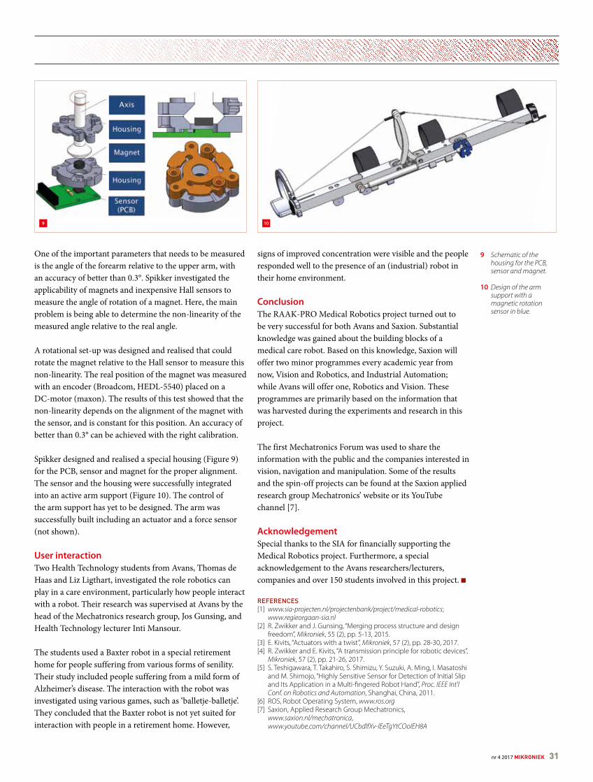
One of the important parameters that needs to be measured is the angle of the forearm relative to the upper arm, with an accuracy of better than 0.3°. Spikker investigated the applicability of magnets and inexpensive Hall sensors to measure the angle of rotation of a magnet. Here, the main problem is being able to determine the non-linearity of the measured angle relative to the real angle.
A rotational set-up was designed and realised that could rotate the magnet relative to the Hall sensor to measure this non-linearity. The real position of the magnet was measured with an encoder (Broadcom, HEDL-5540) placed on a DC-motor (maxon). The results of this test showed that the non-linearity depends on the alignment of the magnet with the sensor, and is constant for this position. An accuracy of better than 0.3° can be achieved with the right calibration.
Spikker designed and realised a special housing (Figure 9) for the PCB, sensor and magnet for the proper alignment. The sensor and the housing were successfully integrated into an active arm support (Figure 10). The control of the arm support has yet to be designed. The arm was successfully built including an actuator and a force sensor (not shown).
User interactionTwo Health Technology students from Avans, Thomas de Haas and Liz Ligthart, investigated the role robotics can play in a care environment, particularly how people interact with a robot. Their research was supervised at Avans by the head of the Mechatronics research group, Jos Gunsing, and Health Technology lecturer Inti Mansour.
The students used a Baxter robot in a special retirement home for people suffering from various forms of senility. Their study included people suffering from a mild form of Alzheimer’s disease. The interaction with the robot was investigated using various games, such as ‘balletje-balletje’. They concluded that the Baxter robot is not yet suited for interaction with people in a retirement home. However,
signs of improved concentration were visible and the people responded well to the presence of an (industrial) robot in their home environment.
ConclusionThe RAAK-PRO Medical Robotics project turned out to be very successful for both Avans and Saxion. Substantial knowledge was gained about the building blocks of a medical care robot. Based on this knowledge, Saxion will offer two minor programmes every academic year from now, Vision and Robotics, and Industrial Automation; while Avans will offer one, Robotics and Vision. These programmes are primarily based on the information that was harvested during the experiments and research in this project.
The first Mechatronics Forum was used to share the information with the public and the companies interested in vision, navigation and manipulation. Some of the results and the spin-off projects can be found at the Saxion applied research group Mechatronics’ website or its YouTube channel [7].
AcknowledgementSpecial thanks to the SIA for financially supporting the Medical Robotics project. Furthermore, a special acknowledgement to the Avans researchers/lecturers, companies and over 150 students involved in this project.
REFERENCES[1] www.sia-projecten.nl/projectenbank/project/medical-robotics;
www.regieorgaan-sia.nl[2] R. Zwikker and J. Gunsing, “Merging process structure and design
freedom”, Mikroniek, 55 (2), pp. 5-13, 2015. [3] E. Kivits, “Actuators with a twist”, Mikroniek, 57 (2), pp. 28-30, 2017. [4] R. Zwikker and E. Kivits, “A transmission principle for robotic devices”,
Mikroniek, 57 (2), pp. 21-26, 2017. [5] S. Teshigawara, T. Takahiro, S. Shimizu, Y. Suzuki, A. Ming, I. Masatoshi
and M. Shimojo, “Highly Sensitive Sensor for Detection of Initial Slip and Its Application in a Multi-fingered Robot Hand”, Proc. IEEE Int'l Conf. on Robotics and Automation, Shanghai, China, 2011.
[6] ROS, Robot Operating System, www.ros.org[7] Saxion, Applied Research Group Mechatronics,
www.saxion.nl/mechatronica, www.youtube.com/channel/UCbdlfXv-lEeTgYtCOoIEH8A
9 Schematic of the housing for the PCB, sensor and magnet.
10 Design of the arm support with a magnetic rotation sensor in blue.
9 10
nr 4 2017 MIKRONIEK 31
SMART CALIBRATION SOLUTION FOR INLINE ATOMIC FORCE MICROSCOPY
VIRTUAL STANDARDS, REAL ADVANTAGES
Accurate measurements with an atomic force microscope (AFM) can only be obtained when the AFM itself is even more accurate and therefore state-of-the-art calibration of the 3D measurement space is required. In practice, this is performed by a separate calibration of the lateral (X and Y) axes and the height (Z) axis. A novel calibration approach is described based on highly linear piezos that eliminates the drawbacks of conventional techniques. The approach will be demonstrated with experimental results.
IntroductionManufacturing processes are currently capable of controlled fabrication of surface features on the nanometer scale. Nanostructures to provide hydrophobic or self-cleaning behaviour and engineered nanoparticles are just a few examples. Since the functionality of such products is closely linked to the exact geometry of the nanoscale features, accurate measurements are required to monitor the product quality and control and optimise the production process.
Atomic force microscopy (AFM) is one key technique to accurately measure properties of surfaces or particles on the nanometer scale. An AFM uses a tiny mechanical probe to scan the contours of a surface line-by-line in order to capture the shape of the surface. While scanning over the surface in the lateral (X and Y) directions the local surface height (Z coordinate) is measured.
An AFM is often used as a reference tool for nanoscale measurements since this is the only instrument that is capable of directly providing traceable 3D (actually 2.5D) measurement data with (sub)nanometer accuracy. Application of an AFM within the production processes itself is still challenging but first results have been demonstrated [1].
Obviously, accurate measurements with an AFM can only be obtained when the AFM itself is even more accurate and therefore state-of-the-art calibration of the 3D measurement space is required. In practice, this is performed by a separate calibration of the lateral (X and Y) axes and the height (Z) axis.
ApplicationsWithin the European 7th Framework Programme the aim4np (automated inline metrology for nanoscale
RICHARD KOOPS, MARIJN VAN VEGHEL AND ARTHUR VAN DE NES
AUTHORS’ NOTE
Richard Koops, Marijn van Veghel and Arthur van de Nes are all with the VSL Dutch Metrology Institute, based in Delft, the Netherlands.
production) project team [1] has implemented a measurement concept based on a robotically controlled measurement platform that is positioned over a product in the production environment (Figure 1).
The instrumentation on the platform will be used to accurately measure critical-to-quality product properties, like areal surface texture, already in the production phase to enable quality assessment at the early stages of manufacturing. Since the measurement data from the metrology platform will be used for quality assessment and ultimately control of the production process parameters, this data must be reliable. The metrology instrumentation therefore has to be calibrated.
Additionally, the aim4np metrology platform is intended to be used to perform inline measurements in a continuous
1 The aim4np project team has developed a robotically controlled metrology platform for inline measurement of products. The white-light interferometer (WLI) and atomic force microscope (AFM) are used, respectively, for global optical inspection and subsequent high-resolution measurements.
1
32 MIKRONIEK nr 4 2017
2 An AFM scan on a conventional step-height standard of nominally 70 nm. Crosstalk between the height axis and the lateral axes results in a curved background that deteriorates the accuracy of the height calibration.
production line where the downtime should be minimised. The calibration and regular recalibration should therefore be performed in-situ at the production site. Compared to tightly controlled laboratory conditions, at a production site the conditions are less well-defined; this pose a challenge to realise the required accuracy at the nanometer level.
Another application is related to the development of metrology for nanoparticles [2]. Whether or not a particle can be classified as a nanoparticle, depends on its exact size. Since there is specific regulation for handling and use of nanoparticles, instrumentation is required that can measure such products with sufficient accuracy. Again, AFM is one the instruments of choice for this application but requires accurate calibration itself.
Conventional AFM calibrationFrom the inception of the first scanning probe microscope [3], the actuation mechanism to translate and control the position of the probe (or sample) is traditionally based on piezo materials because these enable the required subnanometer resolution and control. In order to realise a useful lateral range of typically 100 µm and a 10 µm height range, ceramic piezo materials with a high sensitivity are selected since these allow compact and potentially fast scanner designs. However, the response of these piezo materials is dependent on the range, rate and history of the applied voltage. The resulting non-linear and hysteretic behaviour gives rise to a distorted measurement space.
Moreover, the sensitivity of these piezos can decrease over time due to depolarisation. Accurate positioning based on the actuation voltage is therefore challenging. Open-loop piezo scanners can be linearised by software and/or additional strain gauge sensors but accuracy on the nanometer level can only be obtained by regular calibration with traceable techniques or standards.
HeightConventional calibration of the height axis of an AFM is performed by physical step-height standards. The height of the fabricated step features is either calibrated by interference microscopes or by high-end metrology AFMs
equipped with laser interferometers. The drawback of using such standards for AFM calibration is that they require a relatively large lateral scanning range in order to capture the entire feature. Since the three AFM axes are never completely independent, a large lateral scan suffers from crosstalk between the height axis and the lateral axes (Figure 2). This is visible as a curved background in the final measurement and deteriorates the accuracy of the height calibration.
Additionally, the non-linear response of the height axis results in different sensitivity coefficients depending on the range and requires a set of step-height standards to determine the behaviour for different height ranges. Furthermore, the step structures are difficult to manufacture, susceptible to contamination and difficult to handle in a production environment. Finally, the availability of physical step-height standards for ranges below 5 nm is non-existent, providing a challenge to accurately calibrate features of this size and smaller.
LateralConventional physical calibration standards for the lateral scale are available in the form of 1D or 2D periodic patterns. The most accurate calibration of these physical standards themselves is provided by traceable diffraction measurements and by high-end metrology AFMs. The result of such a calibration is the average pitch over the investigated area where effects from local imperfections on the standard are averaged out. The measurement uncertainty for the calibrated average pitch can therefore easily be smaller than 0.1 nm.
Since the structures are typically fabricated by interference of light, the wavelengths of available light sources provide a lower limit on the pitch of the structures that can be fabricated economically by this method. Hence, pitches smaller than 100-200 nm are not readily available. As a result, accurate calibration of small scanning areas cannot be performed with these types of standards, simply because the number of calibrated features in the image becomes too small and irregularities of the imaged features become relevant for the measurement uncertainty (Figure 3). Therefore, the calibration becomes less accurate for smaller scan sizes and is not even defined for ranges smaller than the pitch. Formal traceability for these scanning areas can therefore not be provided by these types of standards.
In addition, these nanostructured surfaces are very delicate and susceptible to contamination and damage; they are mainly intended for use in controlled environments by trained personnel. These restrictions make the application of conventional lateral calibration standards less useful in a production environment.
2
nr 4 2017 MIKRONIEK 33
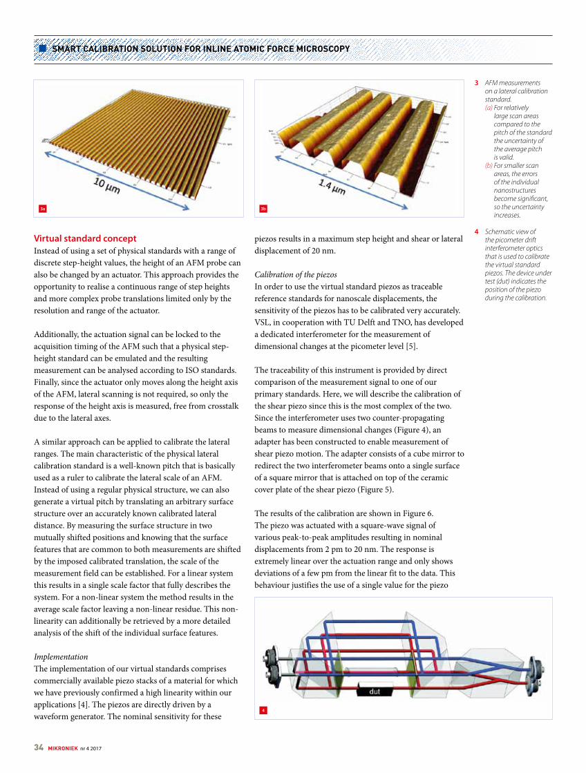
SMART CALIBRATION SOLUTION FOR INLINE ATOMIC FORCE MICROSCOPY
Virtual standard conceptInstead of using a set of physical standards with a range of discrete step-height values, the height of an AFM probe can also be changed by an actuator. This approach provides the opportunity to realise a continuous range of step heights and more complex probe translations limited only by the resolution and range of the actuator.
Additionally, the actuation signal can be locked to the acquisition timing of the AFM such that a physical step-height standard can be emulated and the resulting measurement can be analysed according to ISO standards. Finally, since the actuator only moves along the height axis of the AFM, lateral scanning is not required, so only the response of the height axis is measured, free from crosstalk due to the lateral axes.
A similar approach can be applied to calibrate the lateral ranges. The main characteristic of the physical lateral calibration standard is a well-known pitch that is basically used as a ruler to calibrate the lateral scale of an AFM. Instead of using a regular physical structure, we can also generate a virtual pitch by translating an arbitrary surface structure over an accurately known calibrated lateral distance. By measuring the surface structure in two mutually shifted positions and knowing that the surface features that are common to both measurements are shifted by the imposed calibrated translation, the scale of the measurement field can be established. For a linear system this results in a single scale factor that fully describes the system. For a non-linear system the method results in the average scale factor leaving a non-linear residue. This non-linearity can additionally be retrieved by a more detailed analysis of the shift of the individual surface features.
ImplementationThe implementation of our virtual standards comprises commercially available piezo stacks of a material for which we have previously confirmed a high linearity within our applications [4]. The piezos are directly driven by a waveform generator. The nominal sensitivity for these
piezos results in a maximum step height and shear or lateral displacement of 20 nm.
Calibration of the piezosIn order to use the virtual standard piezos as traceable reference standards for nanoscale displacements, the sensitivity of the piezos has to be calibrated very accurately. VSL, in cooperation with TU Delft and TNO, has developed a dedicated interferometer for the measurement of dimensional changes at the picometer level [5].
The traceability of this instrument is provided by direct comparison of the measurement signal to one of our primary standards. Here, we will describe the calibration of the shear piezo since this is the most complex of the two. Since the interferometer uses two counter-propagating beams to measure dimensional changes (Figure 4), an adapter has been constructed to enable measurement of shear piezo motion. The adapter consists of a cube mirror to redirect the two interferometer beams onto a single surface of a square mirror that is attached on top of the ceramic cover plate of the shear piezo (Figure 5).
The results of the calibration are shown in Figure 6. The piezo was actuated with a square-wave signal of various peak-to-peak amplitudes resulting in nominal displacements from 2 pm to 20 nm. The response is extremely linear over the actuation range and only shows deviations of a few pm from the linear fit to the data. This behaviour justifies the use of a single value for the piezo
3 AFM measurements on a lateral calibration standard.
(a) For relatively large scan areas compared to the pitch of the standard the uncertainty of the average pitch is valid.
(b) For smaller scan areas, the errors of the individual nanostructures become significant, so the uncertainty increases.
4 Schematic view of the picometer drift interferometer optics that is used to calibrate the virtual standard piezos. The device under test (dut) indicates the position of the piezo during the calibration.
3a 3b
4
34 MIKRONIEK nr 4 2017
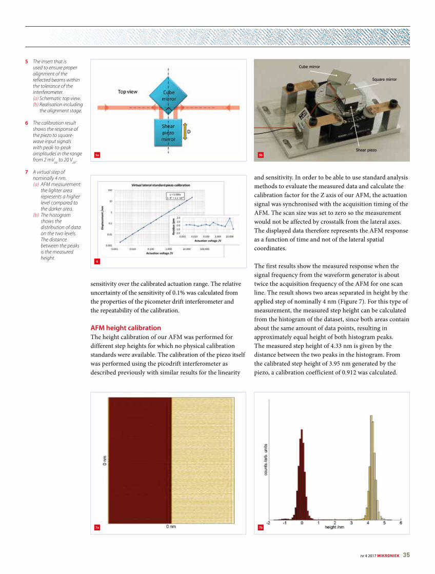
sensitivity over the calibrated actuation range. The relative uncertainty of the sensitivity of 0.1% was calculated from the properties of the picometer drift interferometer and the repeatability of the calibration.
AFM height calibrationThe height calibration of our AFM was performed for different step heights for which no physical calibration standards were available. The calibration of the piezo itself was performed using the picodrift interferometer as described previously with similar results for the linearity
and sensitivity. In order to be able to use standard analysis methods to evaluate the measured data and calculate the calibration factor for the Z axis of our AFM, the actuation signal was synchronised with the acquisition timing of the AFM. The scan size was set to zero so the measurement would not be affected by crosstalk from the lateral axes. The displayed data therefore represents the AFM response as a function of time and not of the lateral spatial coordinates.
The first results show the measured response when the signal frequency from the waveform generator is about twice the acquisition frequency of the AFM for one scan line. The result shows two areas separated in height by the applied step of nominally 4 nm (Figure 7). For this type of measurement, the measured step height can be calculated from the histogram of the dataset, since both areas contain about the same amount of data points, resulting in approximately equal height of both histogram peaks. The measured step height of 4.33 nm is given by the distance between the two peaks in the histogram. From the calibrated step height of 3.95 nm generated by the piezo, a calibration coefficient of 0.912 was calculated.
5 The insert that is used to ensure proper alignment of the reflected beams within the tolerance of the interferometer.
(a) Schematic top view. (b) Realisation including
the alignment stage.
6 The calibration result shows the response of the piezo to square-wave input signals with peak-to-peak amplitudes in the range from 2 mVpp to 20 Vpp.
7 A virtual step of nominally 4 nm.
(a) AFM measurement: the lighter area represents a higher level compared to the darker area.
(b) The histogram shows the distribution of data on the two levels. The distance between the peaks is the measured height.
5a
6
5b
7a 7b
nr 4 2017 MIKRONIEK 35
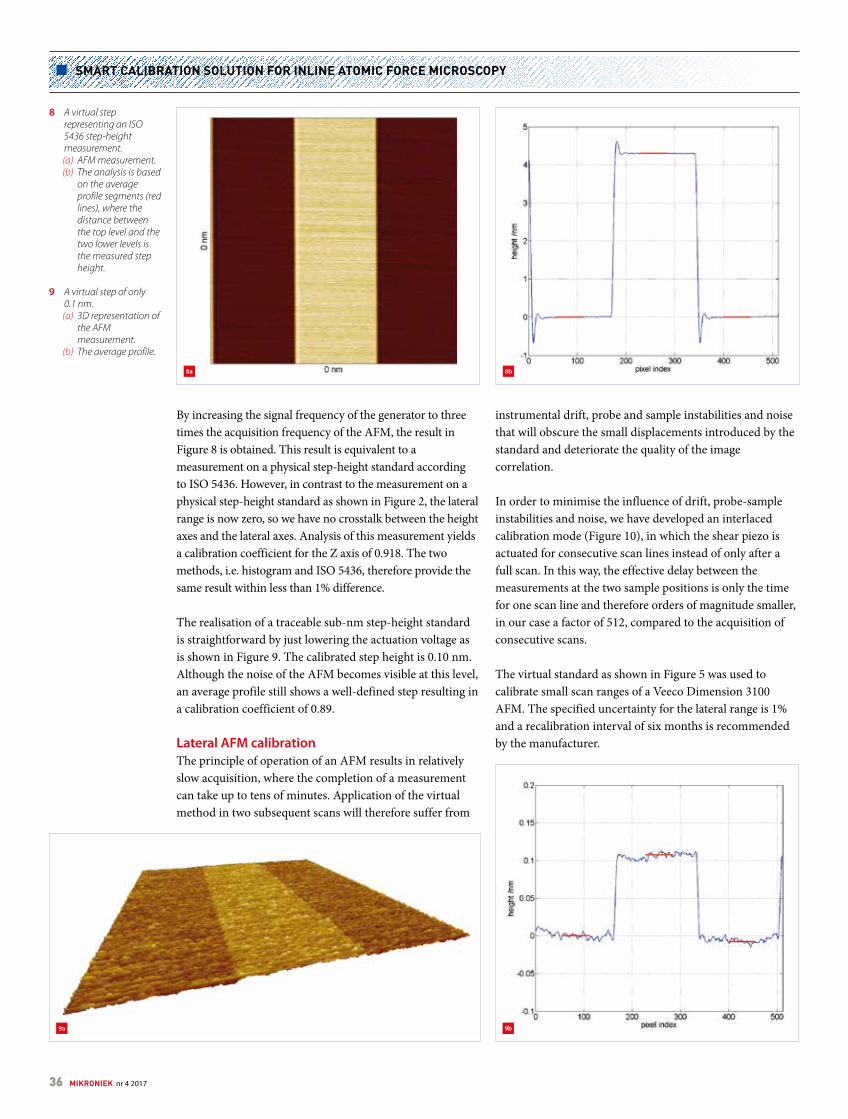
SMART CALIBRATION SOLUTION FOR INLINE ATOMIC FORCE MICROSCOPY
By increasing the signal frequency of the generator to three times the acquisition frequency of the AFM, the result in Figure 8 is obtained. This result is equivalent to a measurement on a physical step-height standard according to ISO 5436. However, in contrast to the measurement on a physical step-height standard as shown in Figure 2, the lateral range is now zero, so we have no crosstalk between the height axes and the lateral axes. Analysis of this measurement yields a calibration coefficient for the Z axis of 0.918. The two methods, i.e. histogram and ISO 5436, therefore provide the same result within less than 1% difference.
The realisation of a traceable sub-nm step-height standard is straightforward by just lowering the actuation voltage as is shown in Figure 9. The calibrated step height is 0.10 nm. Although the noise of the AFM becomes visible at this level, an average profile still shows a well-defined step resulting in a calibration coefficient of 0.89.
Lateral AFM calibrationThe principle of operation of an AFM results in relatively slow acquisition, where the completion of a measurement can take up to tens of minutes. Application of the virtual method in two subsequent scans will therefore suffer from
instrumental drift, probe and sample instabilities and noise that will obscure the small displacements introduced by the standard and deteriorate the quality of the image correlation.
In order to minimise the influence of drift, probe-sample instabilities and noise, we have developed an interlaced calibration mode (Figure 10), in which the shear piezo is actuated for consecutive scan lines instead of only after a full scan. In this way, the effective delay between the measurements at the two sample positions is only the time for one scan line and therefore orders of magnitude smaller, in our case a factor of 512, compared to the acquisition of consecutive scans.
The virtual standard as shown in Figure 5 was used to calibrate small scan ranges of a Veeco Dimension 3100 AFM. The specified uncertainty for the lateral range is 1% and a recalibration interval of six months is recommended by the manufacturer.
8a
8 A virtual step representing an ISO 5436 step-height measurement.
(a) AFM measurement. (b) The analysis is based
on the average profile segments (red lines), where the distance between the top level and the two lower levels is the measured step height.
9 A virtual step of only 0.1 nm.
(a) 3D representation of the AFM measurement.
(b) The average profile.
9a 9b
8b
36 MIKRONIEK nr 4 2017
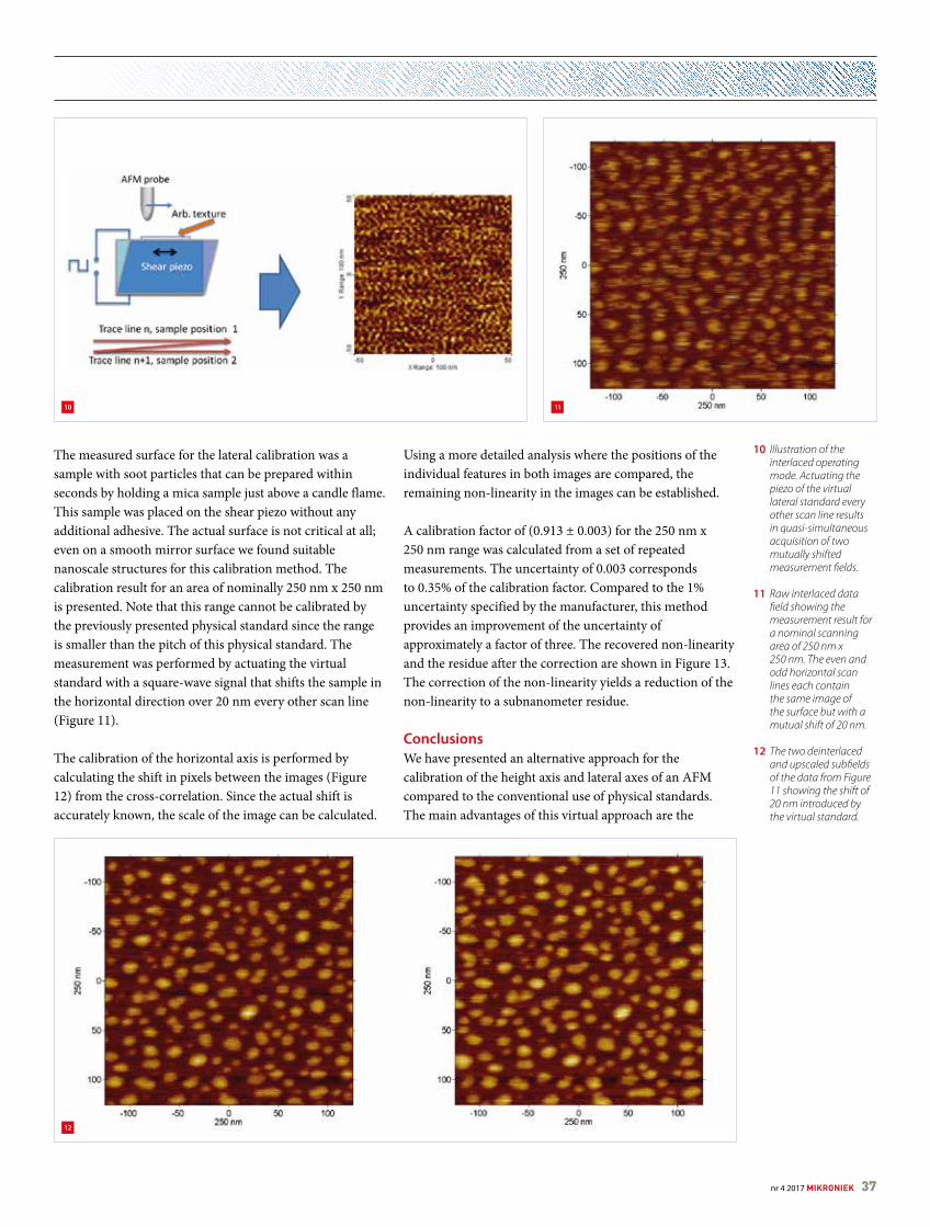
The measured surface for the lateral calibration was a sample with soot particles that can be prepared within seconds by holding a mica sample just above a candle flame. This sample was placed on the shear piezo without any additional adhesive. The actual surface is not critical at all; even on a smooth mirror surface we found suitable nanoscale structures for this calibration method. The calibration result for an area of nominally 250 nm x 250 nm is presented. Note that this range cannot be calibrated by the previously presented physical standard since the range is smaller than the pitch of this physical standard. The measurement was performed by actuating the virtual standard with a square-wave signal that shifts the sample in the horizontal direction over 20 nm every other scan line (Figure 11).
The calibration of the horizontal axis is performed by calculating the shift in pixels between the images (Figure 12) from the cross-correlation. Since the actual shift is accurately known, the scale of the image can be calculated.
Using a more detailed analysis where the positions of the individual features in both images are compared, the remaining non-linearity in the images can be established.
A calibration factor of (0.913 ± 0.003) for the 250 nm x 250 nm range was calculated from a set of repeated measurements. The uncertainty of 0.003 corresponds to 0.35% of the calibration factor. Compared to the 1% uncertainty specified by the manufacturer, this method provides an improvement of the uncertainty of approximately a factor of three. The recovered non-linearity and the residue after the correction are shown in Figure 13. The correction of the non-linearity yields a reduction of the non-linearity to a subnanometer residue.
ConclusionsWe have presented an alternative approach for the calibration of the height axis and lateral axes of an AFM compared to the conventional use of physical standards. The main advantages of this virtual approach are the
10 Illustration of the interlaced operating mode. Actuating the piezo of the virtual lateral standard every other scan line results in quasi-simultaneous acquisition of two mutually shifted measurement fields.
11 Raw interlaced data field showing the measurement result for a nominal scanning area of 250 nm x 250 nm. The even and odd horizontal scan lines each contain the same image of the surface but with a mutual shift of 20 nm.
12 The two deinterlaced and upscaled subfields of the data from Figure 11 showing the shift of 20 nm introduced by the virtual standard.
10 11
12
nr 4 2017 MIKRONIEK 37
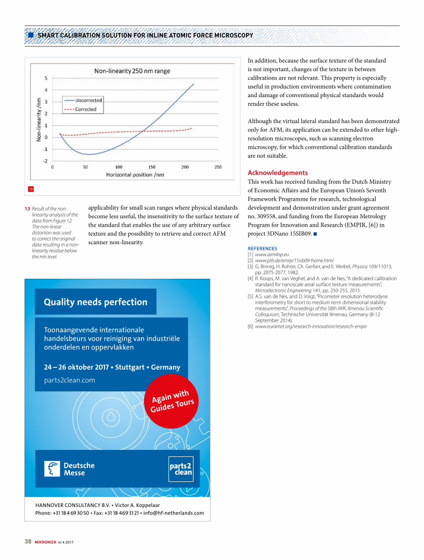
SMART CALIBRATION SOLUTION FOR INLINE ATOMIC FORCE MICROSCOPY
applicability for small scan ranges where physical standards become less useful, the insensitivity to the surface texture of the standard that enables the use of any arbitrary surface texture and the possibility to retrieve and correct AFM scanner non-linearity.
In addition, because the surface texture of the standard is not important, changes of the texture in between calibrations are not relevant. This property is especially useful in production environments where contamination and damage of conventional physical standards would render these useless.
Although the virtual lateral standard has been demonstrated only for AFM, its application can be extended to other high-resolution microscopes, such as scanning electron microscopy, for which conventional calibration standards are not suitable.
AcknowledgementsThis work has received funding from the Dutch Ministry of Economic Affairs and the European Union’s Seventh Framework Programme for research, technological development and demonstration under grant agreement no. 309558, and funding from the European Metrology Program for Innovation and Research (EMPIR, [6]) in project 3DNano 15SIB09.
REFERENCES[1] www.aim4np.eu[2] www.ptb.de/emrp/15sib09-home.html[3] G. Binnig, H. Rohrer, Ch. Gerber, and E. Weibel, Physica 109/11013,
pp. 2075-2077, 1982.[4] R. Koops, M. van Veghel, and A. van de Nes, “A dedicated calibration
standard for nanoscale areal surface texture measurements”, Microelectronic Engineering 141, pp. 250-255, 2015.
[5] A.S. van de Nes, and D. Voigt, “Picometer resolution heterodyne interferometry for short to medium term dimensional stability measurements”, Proceedings of the 58th IWK, Ilmenau Scientific Colloquium, Technische Universität Ilmenau, Germany (8-12 September 2014).
[6] www.euramet.org/research-innovation/research-empir
13 Result of the non-linearity analysis of the data from Figure 12. The non-linear distortion was used to correct the original data resulting in a non-linearity residue below the nm level.
13
Quality needs perfection
HANNOVER CONSULTANCY B.V. • Victor A. Koppelaar Phone: +31 18 4 69 30 50 • Fax: +31 18 469 31 21 • [email protected]
Toonaangevende internationale handelsbeurs voor reiniging van industriële onderdelen en oppervlakken
24 – 26 oktober 2017 ▪ Stuttgart ▪ Germany
parts2clean.com
Again with
Guides Tours
38 MIKRONIEK nr 4 2017
TAPPING INTO A NEW DSPE MEMBER’S EXPERTISE
TEN Flecs – contract manufacturer for thinfilm productsTEN Flecs is a contract manufacturing facility for thin-film integrated circuits and backplanes based on IGZO (indium gallium zinc oxide) and organic TFT technologies. Target applications are NFC and RFID tags, sensors (fingerprint, X-Ray, temperature), displays (LCD, OLED and EPD) and logic (memory, CMOS). TEN Flecs is based in Troitsk, Moscow, Russia, and has a representative / business development office on the High Tech Campus Eindhoven, the Netherlands.
TEN Flecs is a smallscale manufacturing facility, which transfers to industry the decades of applied R&D experience of its technology partners – Imec (Belgium), Holst Centre (the Netherlands) and FlexEnable (UK). The facility is equipped with Flat Panel Display GEN2.5 Tier 1 manufacturing tools. Partnering with the leading equipment and material suppliers makes the line compatible with the technologies of Asian foundries for efficient rampup when volume demand is secured. The line capacity is up to 10,000 m2 of TFTs a year. The customers are manufacturers of components (such as ready displays) as well as design and brand companies looking for contract (outsource) manufacturing.
High precisionTEN Flecs offers a high level of precision for integrated circuits on large areas, not yet achieved within the standard silicon industry. This opportunity is enabled by a flatpanel display production process applied to microelectronics fabrication. The use of novel metaloxide and organic materials allows TEN Flecs to fabricate microelectronics on motherglass of GEN2.5 size (370 mm x 470 mm). Photolithography with scanner and stepper exposure is used for achieving critical dimensions of 1.53 μm. New materials and switching from wafers to glass with incomparably larger sizes, while preserving high precision and small critical dimensions, enables lower costs of microelectronics and is now highly innovative.
ProductionSmallscale production by TEN Flecs allows seeding new markets while testifying new technologies. When flexible
electronics technologies have been verified for industrial and market success, they can be transferred to a larger production scale. IGZO and organic materials, which enable inherent mechanical flexibility and transparency of electronics, are used as semiconducting layers in thinfilm transistors and can be deposited on large areas with no loss of performance.
INFORMATION TENFLECS.COM
1 Conformable organic LCD (OLCD) demo developed by FlexEnable, a TEN Flecs technology partner.
2 The most recent NFC prototype (128-bit NFC Barcode tag, ISO 14443A) developed by Imec, a TEN Flecs technology partner.
2
The production kickoff is planned to Q4 2018.
TEN GroupTEN Flecs is part of the contract services group of companies TEN (Troitsk Engineering Network) managed by TechnoSpark (professional venturebuilding company).TEN Group also includes:• TEN Electronics contract manufacturer of
new electronics and mechatronics.• TEN Engineering contract service company in
full cycle design & engineering.• TEN Fab contract plastic & metalworking plant. • TEN Additive technologies contract
manufacturer of parts, casings, 3Dplastics.• TEN Optics – contract manufacturer of
advanced optical coatings in visual spectra focused on fluorescent dichroic filters.
• TEN Brading contract brading plant, producing fortified parts in aerospace & automotive industries, building, sport furniture.
• TEN Composites contract manufacturer of carcass, shell and individual parts made of composites.
• TEN Med contract manufacturer of prosthetics and other parts for the medical industry.
1
nr 4 2017 MIKRONIEK 39

ECP² COURSE CALENDAR
ECP2 program powered by euspenThe European Certified Precision Engineering Course Program (ECP2) has been developed to meet the demands in the market for continuous professional development and training of postacademic engineers (B.Sc. or M.Sc. with 210 years of work experience) within the fields of precision engineering and nanotechnology. They can earn certification points by following selected courses. Once participants have earned a total of 45 points, they will be certified. The ECP2 certificate is an industrial standard for professional recognition and acknowledgement of precision engineeringrelated knowledge and skills, and allows the use of the ECP2 title. ECP2EU.WPENGINE.COM
Course providers• Engenia (ENG) WWW.ENGENIA.NL
• The High Tech Institute (HTI) WWW.HIGHTECHINSTITUTE.NL
• Mikrocentrum (MC) WWW.MIKROCENTRUM.NL
• LiS Academy (LiS) WWW.LISACADEMY.NL
• Schout DfM (SCHOUT) WWW.SCHOUT.EU
• Holland Innovative (HI) WWW.HOLLANDINNOVATIVE.NL
• Cranfield University WWW.CRANFIELD.AC.UK
Content partners• Dutch Society for Precision
Engineering (DSPE) WWW.DSPE.NL
• Mechatronics Academy (MA) WWW.MECHATRONICS-ACADEMY.NL
• Technical Training for Professionals (T2Prof )
WWW.T2PROF.NL
• Systems & Software Academy (S&SA)
COURSE(content partner)
ECP2 points Provider Starting date(location, if not Eindhoven, NL)
FOUNDATIONMechatronics System Design part 1 (MA) 5 HTI 2 October 2017Mechatronics System Design part 2 (MA) 5 HTI 9 October 2017Design Principles 3 MC 25 September 2017System Architecting (S&SA) 5 HTI 30 October 2017Design Principles Basic (MA) 5 HTI to be planned (Q2 2018)Motion Control Tuning (MA) 6 HTI 15 November 2017
ADVANCEDMetrology and Calibration of Mechatronic Systems (MA) 3 HTI 7 November 2017Actuation and Power Electronics (MA) 3 HTI 14 November 2017Thermal Effects in Mechatronic Systems (MA) 3 HTI to be planned (Q2 2018)Summer school OptoMechatronics (DSPE/MA) 5 HTI Dynamics and Modelling (MA) 3 HTI 27 november 2017
Manufacturability 5 LiS 30 October 2017 (Leiden, NL)Green Belt Design for Six Sigma 4 HI 20 September 2017
26 Sept. 2017 (Enschede, NL)RF1 Life Data Analysis and Reliability Testing 3 HI 6 November 2017
SPECIFICApplied Optics (T2Prof ) 6.5 HTI 31 October 2017Applied Optics 6.5 MC 14 September 2017Machine Vision for Mechatronic Systems (MA) 2 HTI 11 October 2017Electronics for NonElectronic Engineers – Basics Electricity and Analog Electronics (T2Prof )
6 HTI 9 October 2017
Electronics for NonElectronic Engineers – Basics Digital Electronics (T2Prof )
4 HTI to be planned (Q1 2019)
Modern Optics for Optical Designers (T2Prof ) 10 HTI 19 January 2018Tribology 4 MC 31 October 2017 (Utrecht, NL)
6 March 2018Basics & Design Principles for UltraClean Vacuum (MA) 4 HTI 5 December 2017Experimental Techniques in Mechatronics (MA) 3 HTI to be planned (Q2 2018)Advanced Motion Control (MA) 5 HTI 6 November 2017Advanced Feedforward Control (MA) 2 HTI 4 October 2017Advanced Mechatronic System Design (MA) 6 HTI 22 September 2017Finite Element Method 5 ENG incompanyDesign for Manufacturing – Design Decision Method 3 SCHOUT incompanyPrecision Engineering Industrial Short Course 5 CRANF. UNI. to be planned (Cranfield, UK)
40 MIKRONIEK nr 4 2017
UPCOMING EVENTS4 October 2017, Bussum (NL)15th National Cleanroom DayEvent for cleanroom technology users and suppliers in the fields of micro/nano electronics, healthcare, pharma and food, organised by the Dutch Contamination Control Society, VCCN.
WWW.VCCN.NL
10-12 October 2017, Leuven (BE)Special Interest Group Meeting: Additive ManufacturingThe 4th in a series of joint Special Interest Group meetings between euspen and ASPE on dimensional accuracy and surface finish in additive manufacturing.
WWW.EUSPEN.EU
10-12 October 2017, Karlsruhe (DE)DeburringEXPOSecond edition of trade fair for deburring technology and precision surface finishing.
WWW.DEBURRING-EXPO.COM
23-26 October 2017, Aachen (DE)DSPE Optics Week 2017A unique collaboration by Dutch, German and international organisations comprising a symposium & fair, a demonstration day, and two courses. See the preview on page 5 ff.
WWW.OPTICSWEEK.NL
24-26 October, Stuttgart (DE)Parts2clean 2017International trade fair for industrial parts and surface cleaning.
WWW.PARTS2CLEAN.COM
29 October - 3 November 2017, Charlotte (NC, USA)32th ASPE Annual MeetingMeeting of the American Society for Precision Engineering, introducing new concepts, processes, equipment, and products while highlighting recent advances in precision measurement, design, control, and fabrication. ASML will deliver the keynote address.
ASPE.NET
30 October - 3 November 2017, Leiden (NL)LiS Academy Manufacturability course5Day course (summer schooltype) targeted at young professional engineers with a limited knowledge of and experiences with manufacturing technologies and associated manufacturability aspects.
WWW.LISACADEMY.NL
8-9 November 2017, Glasgow (UK)Special Interest Group Meeting Micro/Nano Manufacturing The focus will be on novel methodological developments in micro and nanoscale manufacturing, i.e., on novel process chains including process optimisation, quality assurance approaches and metrology.
WWW.EUSPEN.EU
15-16 November 2017, Veldhoven (NL)Precision Fair 2017Seventeenth edition of the Benelux premier trade fair and conference on precision engineering, organised by Mikrocentrum.
WWW.PRECISIEBEURS.NL
23 November 2017, Utrecht (NL)Dutch Industrial Suppliers & Customer Awards 2017Event organised by Link Magazine, with awards for best knowledge supplier and best logistics supplier, and the Best Customer Award.
WWW.LINKMAGAZINE.NL
12-13 December 2017, Amsterdam (NL)International MicroNanoConference 2017Microfluidics, photonics and nanoinstrumentation are main topics of this industry and applicationoriented conference, exhibition and demo event.
WWW.MICRONANOCONFERENCE.ORG
13-14 December 2017, Den Bosch (NL)AgriFoodTech 2017Second edition of event featuring innovations within the agri and food sectors, such as sensors, drones, autonomous robots, smart farming, big data, vision technology and smart LEDs. The focus is on efficient, effective and sustainable production, in machine design and food processing as well as in the field.
WWW.AGRIFOODTECH.NL
21-23 March 2018, Dresden (DE)Conference on Thermal Issues in Machine ToolsThis conference is organised by CRC/TR 96 and euspen (Special Interest Group Thermal Issues), which have been working to solve the conflict between reducing energy consumption and increasing accuracy and productivity in machining since 2011.
WWW.EUSPEN.EU
nr 4 2017 MIKRONIEK 41
NEWS
The 2017 edition will focus on digitalisation, networking and the production operations of tomorrow, i.e., on Industry 4.0 and the Internet of Things. EMO Hannover 2017 will be held from 18 to 23 September in Hannover, Germany, and is organised by the German Machine Tool Builders’ Association (VDW), located in Frankfurt am Main, on behalf of the European European Association of the Machine Tool Industries, Cecimo.
EMO preview
(Courtesy: Deutsche Messe)
EMO Hannover claims exhibitors have since long aligned their innovation cycles to the fair’s calendar. “As a result, more innovations are unveiled here than at any other trade fair in the industry – which in turn makes EMO Hannover a key point of reference for the decision makers in the production technology segment.” Below, a preview of the innovations introduced by Renishaw, Cellro and Hembrug.
Integrated measurementRenishaw, a world leader in precision engineering technologies, will be exhibiting its extensive range of metrology and additive manufacturing systems on two stands at EMO Hannover 2017. Intelligent machining processes are critical to companies that want to exploit the full benefits of Industry 4.0; hence, Renishaw will demonstrate the power of integrating its latest measurement technologies within a manufacturing process. In addition, it will exhibit software and systems for metal part manufacture in the EMO’s new Additive Manufacturing Zone.
Products highlighted will include a new contact scanning system for CNC machine tools, new software for the Equator flexible gauge which allows users to fully integrate the system with CNC machine tools, new onmachine and mobile apps that simplify the use of machine tool probing, an enhanced noncontact tool setter for machining centres, a new multiprobe optical interface system, a new surface finish probe for coordinate measuring machines (CMMs), and new software that enhances the functionality of Renishaw’s XM60 multiaxis calibration system.
On display will be, for example, a new member of Renishaw’s SPRINT product family for onmachine scanning. The new SPRINT system with SupaScan is designed for simple integration into machine tool applications requiring fast workpiece setup, and where overall cycle time is critical, bringing the benefits of scanning technology to the mass market. The system also provides the ability to perform advanced scanning functionality such as monitoring the final condition of a component surface.
Another innovation is a new, improved surface finish measurement probe for use with Renishaw’s multisensor REVO 5axis measurement system on CMMs. The new SFP2 probe allows users to fully integrate surface finish measurement and dimensional inspection on a single CMM, giving advantages over traditional methods requiring a separate process. The
EMO Hannover is the world’s premier trade fair for the metalworking sector, attracting approximately 60% of its exhibitors from outside of Germany. The fair covers products and services throughout all metalworking production areas, from machine tools and production systems for cutting and forming which are at the heart of machining, precision tools, accessories and controller technology, to system elements and components for automated manufacturing.
42 MIKRONIEK nr 4 2017
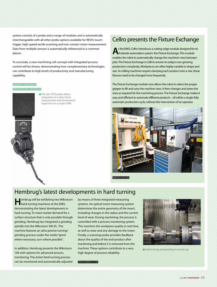
Cellro presents the Fixture Exchange
At the EMO, Cellro introduces a cuttingedge module designed for its Xcelerate automation system: the Fixture Exchange. This module
enables the robot to automatically change the machine’s vises between jobs. The Fixture Exchange is Cellro’s answer to today’s evergrowing production complexity. Workpieces are often highly variable in shape and size. As milling machines require clamping each product onto a vise, these fixtures need to be changed more frequently.
The Fixture Exchange module now allows the robot to select the proper gripper to lift and carry the machine vises. It then changes and stores the vises as required for the machining process. The Fixture Exchange makes it easy and efficient to automate different products – all within a single fully automatic production cycle, without the intervention of an operator.
WWW.CELLRO.COM
system consists of a probe and a range of modules and is automatically interchangeable with all other probe options available for REVO; touchtrigger, highspeed tactile scanning and noncontact vision measurement. Data from multiple sensors is automatically referenced to a common datum.
To conclude, a new machining cell concept with integrated process control will be shown, demonstrating how complementary technologies can contribute to high levels of productivity and manufacturing capability.
WWW.EMO-HANNOVER.DE
WWW.RENISHAW.COM/EMOHUB
The new SFP2 probe allows integration of surface finish measurement and dimensional inspection on a single CMM.
Hembrug’s latest developments in hard turning
Hembrug will be exhibiting two Mikroturn hardturning machines at the EMO,
demonstrating the latest developments in hard turning. To meet market demand for a surface structure that is only possible through grinding, Hembrug has integrated a grinding spindle into the Mikroturn 500 XL. This machine features an ultraprecise turning/grinding process under the motto “grind where necessary, turn where possible”.
In addition, Hembrug presents the Mikroturn 100 with options for advanced process monitoring. The entire hardturning process can be monitored and automatically adjusted
by means of three integrated measuring systems. An optical insert measuring system determines the entire geometry of the insert, including changes in the radius and the current level of wear. During machining, the process is controlled with a process monitoring system. This monitors the workpiece quality in real time, as well as wear and any damage to the insert. Finally, a scanning probe provides feedback about the quality of the endproduct after machining and before it is removed from the machine. These options contribute to a very high degree of process reliability.
WWW.HEMBRUG.COM
Hard turning and grinding in one set-up.
nr 4 2017 MIKRONIEK 43
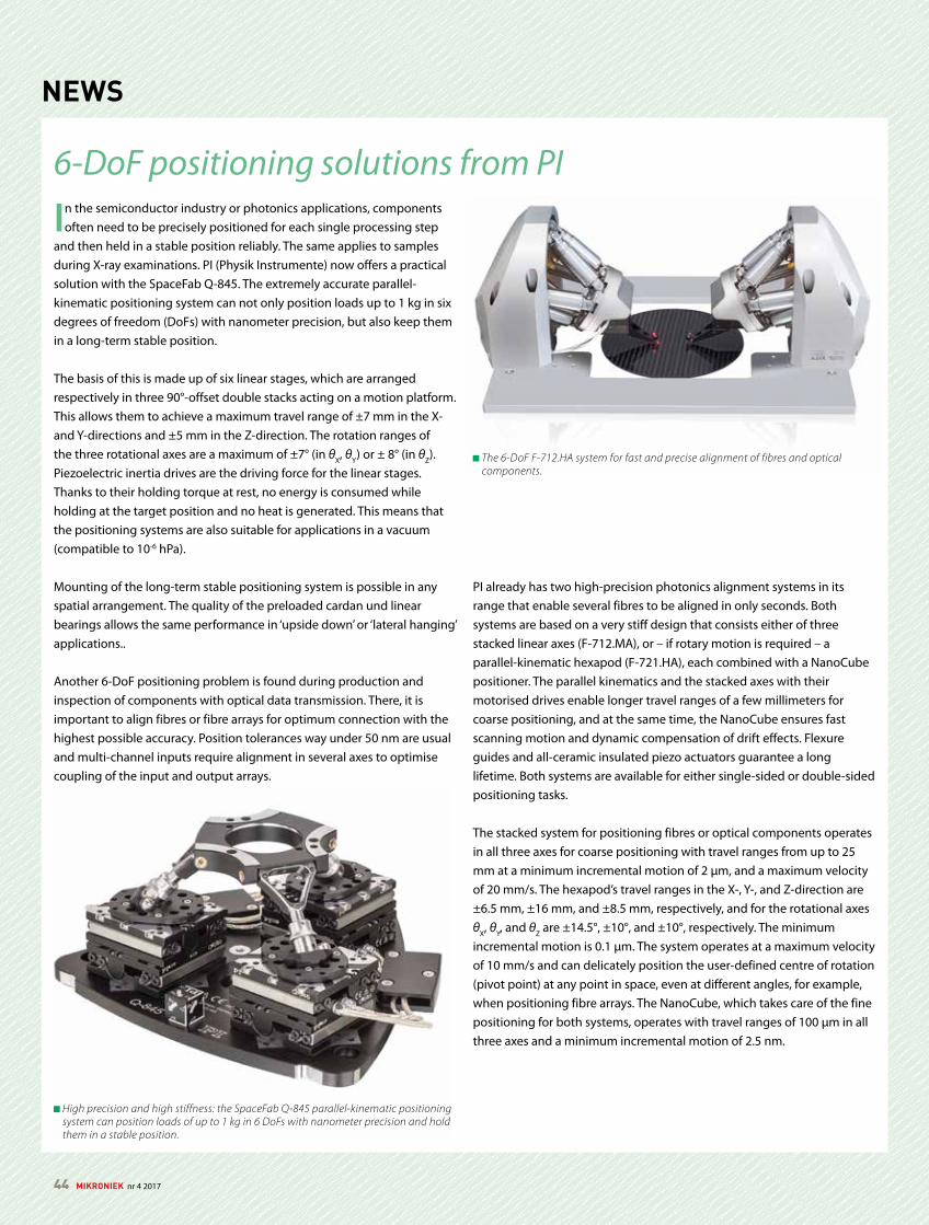
NEWS
In the semiconductor industry or photonics applications, components often need to be precisely positioned for each single processing step
and then held in a stable position reliably. The same applies to samples during Xray examinations. PI (Physik Instrumente) now offers a practical solution with the SpaceFab Q845. The extremely accurate parallelkinematic positioning system can not only position loads up to 1 kg in six degrees of freedom (DoFs) with nanometer precision, but also keep them in a longterm stable position.
The basis of this is made up of six linear stages, which are arranged respectively in three 90°offset double stacks acting on a motion platform. This allows them to achieve a maximum travel range of ±7 mm in the X and Ydirections and ±5 mm in the Zdirection. The rotation ranges of the three rotational axes are a maximum of ±7° (in θX, θY) or ± 8° (in θZ). Piezoelectric inertia drives are the driving force for the linear stages. Thanks to their holding torque at rest, no energy is consumed while holding at the target position and no heat is generated. This means that the positioning systems are also suitable for applications in a vacuum (compatible to 106 hPa).
Mounting of the longterm stable positioning system is possible in any spatial arrangement. The quality of the preloaded cardan und linear bearings allows the same performance in ‘upside down’ or ‘lateral hanging’ applications..
Another 6DoF positioning problem is found during production and inspection of components with optical data transmission. There, it is important to align fibres or fibre arrays for optimum connection with the highest possible accuracy. Position tolerances way under 50 nm are usual and multichannel inputs require alignment in several axes to optimise coupling of the input and output arrays.
6-DoF positioning solutions from PI
PI already has two highprecision photonics alignment systems in its range that enable several fibres to be aligned in only seconds. Both systems are based on a very stiff design that consists either of three stacked linear axes (F712.MA), or – if rotary motion is required – a parallelkinematic hexapod (F721.HA), each combined with a NanoCube positioner. The parallel kinematics and the stacked axes with their motorised drives enable longer travel ranges of a few millimeters for coarse positioning, and at the same time, the NanoCube ensures fast scanning motion and dynamic compensation of drift effects. Flexure guides and allceramic insulated piezo actuators guarantee a long lifetime. Both systems are available for either singlesided or doublesided positioning tasks. The stacked system for positioning fibres or optical components operates in all three axes for coarse positioning with travel ranges from up to 25 mm at a minimum incremental motion of 2 µm, and a maximum velocity of 20 mm/s. The hexapod’s travel ranges in the X, Y, and Zdirection are ±6.5 mm, ±16 mm, and ±8.5 mm, respectively, and for the rotational axes θX, θY, and θZ are ±14.5°, ±10°, and ±10°, respectively. The minimum incremental motion is 0.1 µm. The system operates at a maximum velocity of 10 mm/s and can delicately position the userdefined centre of rotation (pivot point) at any point in space, even at different angles, for example, when positioning fibre arrays. The NanoCube, which takes care of the fine positioning for both systems, operates with travel ranges of 100 µm in all three axes and a minimum incremental motion of 2.5 nm.
High precision and high stiffness: the SpaceFab Q-845 parallel-kinematic positioning system can position loads of up to 1 kg in 6 DoFs with nanometer precision and hold them in a stable position.
The 6-DoF F-712.HA system for fast and precise alignment of fibres and optical components.
44 MIKRONIEK nr 4 2017
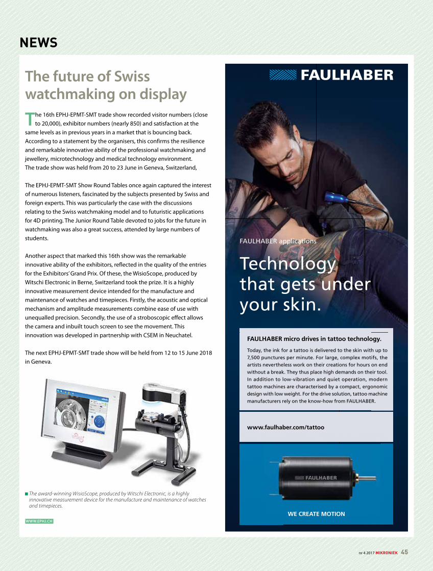
NEWS
Technology that gets under your skin.
FAULHABER applications
FAULHABER micro drives in tattoo technology.
Today, the ink for a tattoo is delivered to the skin with up to 7,500 punctures per minute. For large, complex motifs, the artists nevertheless work on their creations for hours on end without a break. They thus place high demands on their tool. In addition to low-vibration and quiet operation, modern tattoo machines are characterised by a compact, ergonomic design with low weight. For the drive solution, tattoo machine manufacturers rely on the know-how from FAULHABER.
www.faulhaber.com/tattoo
WE CREATE MOTION
dff_170512_anz_tattoo_97x260_en.indd 1 28.07.17 14:45
The award-winning WisioScope, produced by Witschi Electronic, is a highly innovative measurement device for the manufacture and maintenance of watches and timepieces.
The 16th EPHJEPMTSMT trade show recorded visitor numbers (close to 20,000), exhibitor numbers (nearly 850) and satisfaction at the
same levels as in previous years in a market that is bouncing back. According to a statement by the organisers, this confirms the resilience and remarkable innovative ability of the professional watchmaking and jewellery, microtechnology and medical technology environment. The trade show was held from 20 to 23 June in Geneva, Switzerland,
The EPHJEPMTSMT Show Round Tables once again captured the interest of numerous listeners, fascinated by the subjects presented by Swiss and foreign experts. This was particularly the case with the discussions relating to the Swiss watchmaking model and to futuristic applications for 4D printing. The Junior Round Table devoted to jobs for the future in watchmaking was also a great success, attended by large numbers of students.
Another aspect that marked this 16th show was the remarkable innovative ability of the exhibitors, reflected in the quality of the entries for the Exhibitors’ Grand Prix. Of these, the WisioScope, produced by Witschi Electronic in Berne, Switzerland took the prize. It is a highly innovative measurement device intended for the manufacture and maintenance of watches and timepieces. Firstly, the acoustic and optical mechanism and amplitude measurements combine ease of use with unequalled precision. Secondly, the use of a stroboscopic effect allows the camera and inbuilt touch screen to see the movement. This innovation was developed in partnership with CSEM in Neuchatel. The next EPHJEPMTSMT trade show will be held from 12 to 15 June 2018 in Geneva.
WWW.EPHJ.CH
The future of Swiss watchmaking on display
nr 4 2017 MIKRONIEK 45
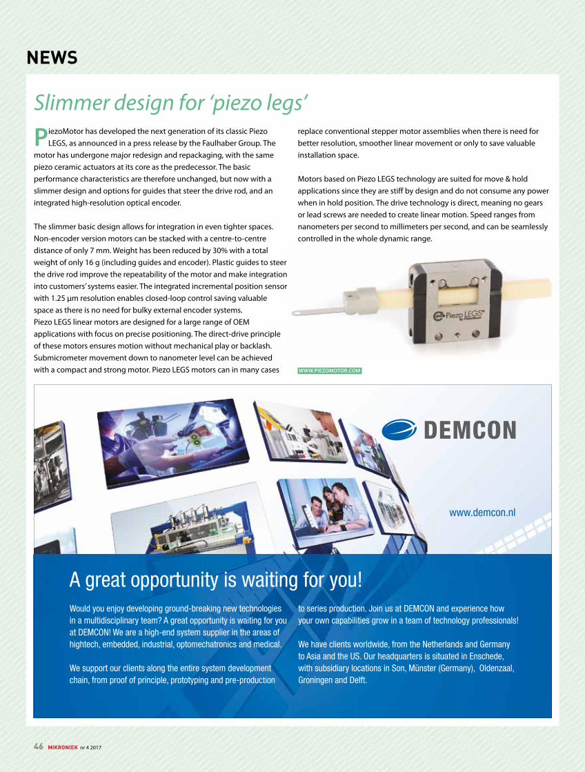
NEWS
Would you enjoy developing ground-breaking new technologies in a multidisciplinary team? A great opportunity is waiting for you at DEMCON! We are a high-end system supplier in the areas of hightech, embedded, industrial, optomechatronics and medical.
We support our clients along the entire system development chain, from proof of principle, prototyping and pre-production
to series production. Join us at DEMCON and experience how your own capabilities grow in a team of technology professionals!
We have clients worldwide, from the Netherlands and Germany to Asia and the US. Our headquarters is situated in Enschede, with subsidiary locations in Son, Münster (Germany), Oldenzaal, Groningen and Delft.
A great opportunity is waiting for you!
www.demcon.nl
PiezoMotor has developed the next generation of its classic Piezo LEGS, as announced in a press release by the Faulhaber Group. The
motor has undergone major redesign and repackaging, with the same piezo ceramic actuators at its core as the predecessor. The basic performance characteristics are therefore unchanged, but now with a slimmer design and options for guides that steer the drive rod, and an integrated highresolution optical encoder.
The slimmer basic design allows for integration in even tighter spaces. Nonencoder version motors can be stacked with a centretocentre distance of only 7 mm. Weight has been reduced by 30% with a total weight of only 16 g (including guides and encoder). Plastic guides to steer the drive rod improve the repeatability of the motor and make integration into customers’ systems easier. The integrated incremental position sensor with 1.25 μm resolution enables closedloop control saving valuable space as there is no need for bulky external encoder systems. Piezo LEGS linear motors are designed for a large range of OEM applications with focus on precise positioning. The directdrive principle of these motors ensures motion without mechanical play or backlash. Submicrometer movement down to nanometer level can be achieved with a compact and strong motor. Piezo LEGS motors can in many cases
Slimmer design for ‘piezo legs’replace conventional stepper motor assemblies when there is need for better resolution, smoother linear movement or only to save valuable installation space.
Motors based on Piezo LEGS technology are suited for move & hold applications since they are stiff by design and do not consume any power when in hold position. The drive technology is direct, meaning no gears or lead screws are needed to create linear motion. Speed ranges from nanometers per second to millimeters per second, and can be seamlessly controlled in the whole dynamic range.
WWW.PIEZOMOTOR.COM
46 MIKRONIEK nr 4 2017
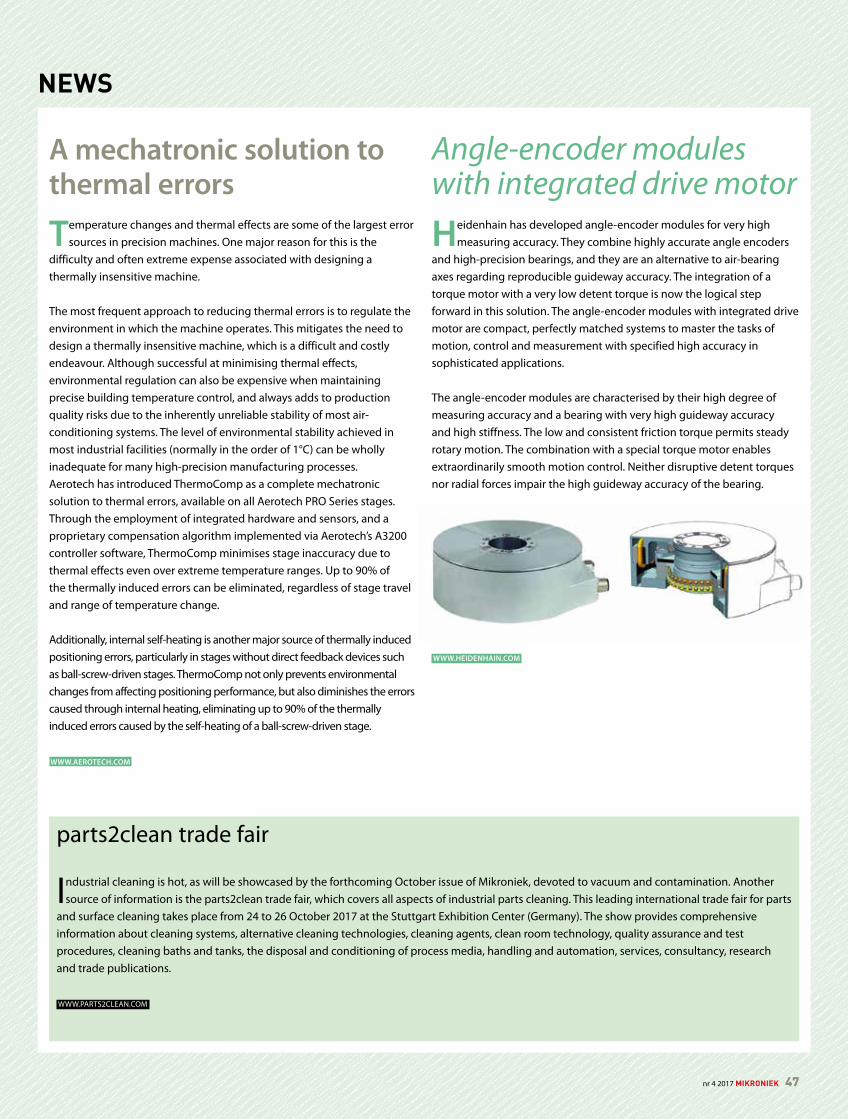
NEWS
parts2clean trade fair
Industrial cleaning is hot, as will be showcased by the forthcoming October issue of Mikroniek, devoted to vacuum and contamination. Another source of information is the parts2clean trade fair, which covers all aspects of industrial parts cleaning. This leading international trade fair for parts
and surface cleaning takes place from 24 to 26 October 2017 at the Stuttgart Exhibition Center (Germany). The show provides comprehensive information about cleaning systems, alternative cleaning technologies, cleaning agents, clean room technology, quality assurance and test procedures, cleaning baths and tanks, the disposal and conditioning of process media, handling and automation, services, consultancy, research and trade publications.
WWW.PARTS2CLEAN.COM
Temperature changes and thermal effects are some of the largest error sources in precision machines. One major reason for this is the
difficulty and often extreme expense associated with designing a thermally insensitive machine.
The most frequent approach to reducing thermal errors is to regulate the environment in which the machine operates. This mitigates the need to design a thermally insensitive machine, which is a difficult and costly endeavour. Although successful at minimising thermal effects, environmental regulation can also be expensive when maintaining precise building temperature control, and always adds to production quality risks due to the inherently unreliable stability of most airconditioning systems. The level of environmental stability achieved in most industrial facilities (normally in the order of 1°C) can be wholly inadequate for many highprecision manufacturing processes.Aerotech has introduced ThermoComp as a complete mechatronic solution to thermal errors, available on all Aerotech PRO Series stages. Through the employment of integrated hardware and sensors, and a proprietary compensation algorithm implemented via Aerotech’s A3200 controller software, ThermoComp minimises stage inaccuracy due to thermal effects even over extreme temperature ranges. Up to 90% of the thermally induced errors can be eliminated, regardless of stage travel and range of temperature change.
Additionally, internal selfheating is another major source of thermally induced positioning errors, particularly in stages without direct feedback devices such as ballscrewdriven stages. ThermoComp not only prevents environmental changes from affecting positioning performance, but also diminishes the errors caused through internal heating, eliminating up to 90% of the thermally induced errors caused by the selfheating of a ballscrewdriven stage.
WWW.AEROTECH.COM
A mechatronic solution to thermal errors
Heidenhain has developed angleencoder modules for very high measuring accuracy. They combine highly accurate angle encoders
and highprecision bearings, and they are an alternative to airbearing axes regarding reproducible guideway accuracy. The integration of a torque motor with a very low detent torque is now the logical step forward in this solution. The angleencoder modules with integrated drive motor are compact, perfectly matched systems to master the tasks of motion, control and measurement with specified high accuracy in sophisticated applications.
The angleencoder modules are characterised by their high degree of measuring accuracy and a bearing with very high guideway accuracy and high stiffness. The low and consistent friction torque permits steady rotary motion. The combination with a special torque motor enables extraordinarily smooth motion control. Neither disruptive detent torques nor radial forces impair the high guideway accuracy of the bearing.
WWW.HEIDENHAIN.COM
Angle-encoder modules with integrated drive motor
nr 4 2017 MIKRONIEK 47
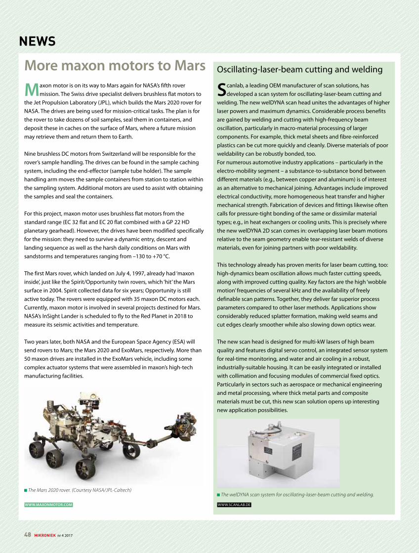
NEWS
Maxon motor is on its way to Mars again for NASA’s fifth rover mission. The Swiss drive specialist delivers brushless flat motors to
the Jet Propulsion Laboratory (JPL), which builds the Mars 2020 rover for NASA. The drives are being used for missioncritical tasks. The plan is for the rover to take dozens of soil samples, seal them in containers, and deposit these in caches on the surface of Mars, where a future mission may retrieve them and return them to Earth.
Nine brushless DC motors from Switzerland will be responsible for the rover’s sample handling. The drives can be found in the sample caching system, including the endeffector (sample tube holder). The sample handling arm moves the sample containers from station to station within the sampling system. Additional motors are used to assist with obtaining the samples and seal the containers.
For this project, maxon motor uses brushless flat motors from the standard range (EC 32 flat and EC 20 flat combined with a GP 22 HD planetary gearhead). However, the drives have been modified specifically for the mission: they need to survive a dynamic entry, descent and landing sequence as well as the harsh daily conditions on Mars with sandstorms and temperatures ranging from –130 to +70 °C.
The first Mars rover, which landed on July 4, 1997, already had ‘maxon inside’, just like the Spirit/Opportunity twin rovers, which ‘hit’ the Mars surface in 2004. Spirit collected data for six years; Opportunity is still active today. The rovers were equipped with 35 maxon DC motors each. Currently, maxon motor is involved in several projects destined for Mars. NASA’s InSight Lander is scheduled to fly to the Red Planet in 2018 to measure its seismic activities and temperature.
Two years later, both NASA and the European Space Agency (ESA) will send rovers to Mars; the Mars 2020 and ExoMars, respectively. More than 50 maxon drives are installed in the ExoMars vehicle, including some complex actuator systems that were assembled in maxon’s hightech manufacturing facilities.
WWW.MAXONMOTOR.COM
More maxon motors to Mars
The Mars 2020 rover. (Courtesy NASA/JPL-Caltech)
Oscillatinglaserbeam cutting and welding
Scanlab, a leading OEM manufacturer of scan solutions, has developed a scan system for oscillatinglaserbeam cutting and
welding. The new welDYNA scan head unites the advantages of higher laser powers and maximum dynamics. Considerable process benefits are gained by welding and cutting with highfrequency beam oscillation, particularly in macromaterial processing of larger components. For example, thick metal sheets and fibrereinforced plastics can be cut more quickly and cleanly. Diverse materials of poor weldability can be robustly bonded, too.For numerous automotive industry applications – particularly in the electromobility segment – a substancetosubstance bond between different materials (e.g., between copper and aluminum) is of interest as an alternative to mechanical joining. Advantages include improved electrical conductivity, more homogeneous heat transfer and higher mechanical strength. Fabrication of devices and fittings likewise often calls for pressuretight bonding of the same or dissimilar material types; e.g., in heat exchangers or cooling units. This is precisely where the new welDYNA 2D scan comes in: overlapping laser beam motions relative to the seam geometry enable tearresistant welds of diverse materials, even for joining partners with poor weldability.
This technology already has proven merits for laser beam cutting, too: highdynamics beam oscillation allows much faster cutting speeds, along with improved cutting quality. Key factors are the high ‘wobble motion’ frequencies of several kHz and the availability of freely definable scan patterns. Together, they deliver far superior process parameters compared to other laser methods. Applications show considerably reduced splatter formation, making weld seams and cut edges clearly smoother while also slowing down optics wear.
The new scan head is designed for multikW lasers of high beam quality and features digital servo control, an integrated sensor system for realtime monitoring, and water and air cooling in a robust, industriallysuitable housing. It can be easily integrated or installed with collimation and focusing modules of commercial fixed optics. Particularly in sectors such as aerospace or mechanical engineering and metal processing, where thick metal parts and composite materials must be cut, this new scan solution opens up interesting new application possibilities.
WWW.SCANLAB.DE
The welDYNA scan system for oscillating-laser-beam cutting and welding.
48 MIKRONIEK nr 4 2017
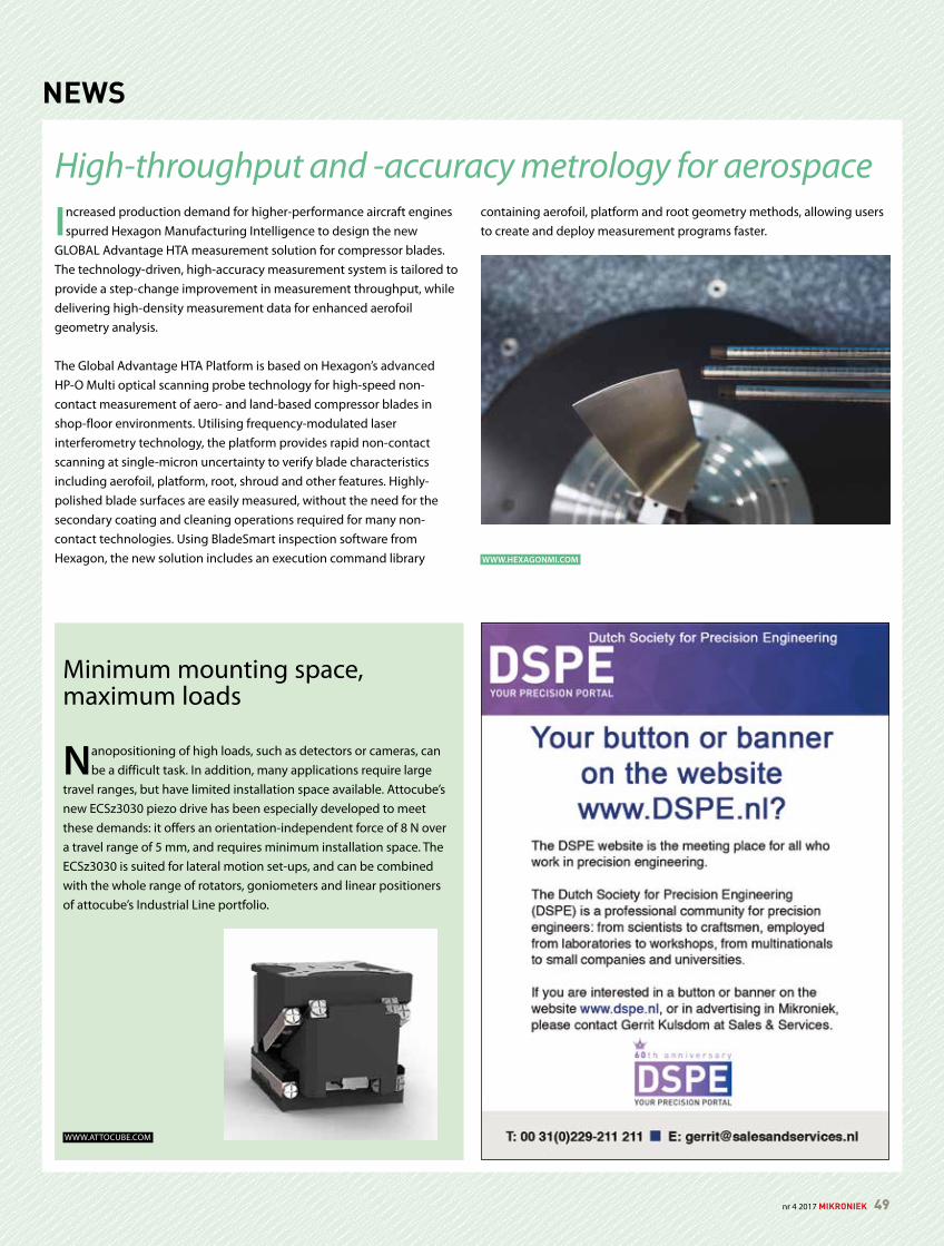
NEWS
Increased production demand for higherperformance aircraft engines spurred Hexagon Manufacturing Intelligence to design the new
GLOBAL Advantage HTA measurement solution for compressor blades. The technologydriven, highaccuracy measurement system is tailored to provide a stepchange improvement in measurement throughput, while delivering highdensity measurement data for enhanced aerofoil geometry analysis.
The Global Advantage HTA Platform is based on Hexagon’s advanced HPO Multi optical scanning probe technology for highspeed noncontact measurement of aero and landbased compressor blades in shopfloor environments. Utilising frequencymodulated laser interferometry technology, the platform provides rapid noncontact scanning at singlemicron uncertainty to verify blade characteristics including aerofoil, platform, root, shroud and other features. Highlypolished blade surfaces are easily measured, without the need for the secondary coating and cleaning operations required for many noncontact technologies. Using BladeSmart inspection software from Hexagon, the new solution includes an execution command library
High-throughput and -accuracy metrology for aerospacecontaining aerofoil, platform and root geometry methods, allowing users to create and deploy measurement programs faster.
WWW.HEXAGONMI.COM
Minimum mounting space, maximum loads
Nanopositioning of high loads, such as detectors or cameras, can be a difficult task. In addition, many applications require large
travel ranges, but have limited installation space available. Attocube’s new ECSz3030 piezo drive has been especially developed to meet these demands: it offers an orientationindependent force of 8 N over a travel range of 5 mm, and requires minimum installation space. The ECSz3030 is suited for lateral motion setups, and can be combined with the whole range of rotators, goniometers and linear positioners of attocube’s Industrial Line portfolio.
WWW.ATTOCUBE.COM
nr 4 2017 MIKRONIEK 49
GUIDEAutomation Technology
Festo BVSchieweg 62 2627 AN DELFTThe NetherlandsT +31 (0)152518890E [email protected] www.festo.nlContact person: Mr. Ing. Richard Huisman
Festo is a leading worldwide supplier of automation technology and the performance leader in industrial training and education programs.
member
Cleanrooms
Brecon GroupKroonstraat 64879 AV EttenLeurT +31 (0)76 504 70 80E [email protected] www.brecon.nl
Brecon Group can attribute a large proportion of its fame as a cleanroom builder to continuity in the delivery of quality products within the semiconductor industry, with ASML as the most important associate in the past decades.
Brecon is active with cleanrooms in a high number of sectors on:* Industrial and pharmaceutical* Healthcare and medical devices
2
2
2
Cleanrooms
Cleanrooms
Connect 2 Cleanrooms BVGraadt van Roggenweg 328344 (Blok D)3531 AH UtrechtNederlandT +31 (0)30 298 2112E [email protected] www.connect2cleanrooms.nl
Our cleanroom solutions are bespoke and scalable, encouraging efficiency through flexible design. We help organisations reduce failure rates by getting it right first time.
member
Development
TNOT + 31 (0)88866 50 00W www.tno.nl
TNO is an independent innovation organisation that connects people and knowledge in order to create the innovations that sustainably boosts the competitiveness of industry and wellbeing of society.
member
Development and Engineering
ACE ingenieurs- & adviesbureauwerktuigbouwkunde en elektrotechniek BVDr. Holtroplaan 46Postbus 7030, 5605 JA Eindhoven5652 XR EindhovenT +31 (0)40 2578300F +31 (0)40 2578397 E [email protected] W www.ace.eu
ACE has developed into a leading engineering and consultancy firm with a strong focus on mechanics and mechatronics. Services include conceptualization, development, engineering and prototyping.
member
Development and Engineering
Segula Technologies Nederland B.V.De Witbogt 25652 AG EindhovenT +31 (0)40 8517 500W www.segula.nl
SEGULA Technologies Nederland BV develops advanced intelligent systems for the High Tech and Automotive industry. As a project organisation, we apply our (engineering) knowledge to nonlinear systems. This knowledge is comprised of systems architecture and modelling, analysis, mechanics, mechatronics, electronics, software, system integration, calibration and validation.
member
50 MIKRONIEK nr 4 2017
GUIDEEducation
Leiden school for Instrument-makers (LiS)Einsteinweg 612333 CC LeidenThe NetherlandsT +31 (0)715681168F +31 (0)715681160E [email protected] www.lis.nl, www.lisacademy.nl
The LiS is a modern level 4 MBO school, with a long history (founded in 1901). The school encourages establishing projects in close cooperation with industry and scientific institutes, allowing for high level “real life” work. Under the name LiSEngineering and LiSAcademy the school accepts contract work and organizes education for others.
member
PAO Techniek en Management
De Bouwcampus TU Delft, gebouw 26 Van der Burghweg 1 2628 CS DelftPostbus 50482600 GA Delft
T +31 (0)152784618E [email protected] www.paotm.nl
Electrical Discharge Machining (EDM)
CVT BVHeiberg 29C5504 PA VeldhovenThe NetherlandsT +31 (0)497 54 10 40E [email protected] www.heinmade.com
Partner high tech industry for wire EDM precision parts. Flexible during day shifts for prototyping. Outside office hours low cost unmanned machining. Call and enjoy our expertise!
member
Ter Hoek VonkerosiePropaanstraat 17463 PN RijssenT +31 (0)548 540807F +31 (0)548 540939E [email protected] www.terhoek.com
INNOVATION OF TOMORROW, INSPIRATION FOR TODAYStaying ahead by always going the extra mile. Based on that philosophy, Ter Hoek produces precision components for the hightech manufacturing industry.
We support customers in developing highquality, custom solutions that can then be seriesproduced with unparalleled accuracy. That is what makes us one of a kind. It is in that combination of innovative customization and repeated precision that we find our passion. Inspired by tomorrow’s innovation, each and every day.
member
Lasers, Light and Nanomotion
Laser 2000 Benelux C.V. Voorbancken 13a 3645 GV VinkeveenPostbus 20, 3645 ZJ VinkeveenT +31(0)297 266 191F +31(0)297 266 134E [email protected] www.laser2000.nl
Laser 2000 Benelux considers it her mission to offer customers the latest photonics technologies available.Our areas of expertise are:• Lasers, scanners and laser
machines for industry and research• Light metrology instruments for
LED and luminaire industries• Light sources for scientific
applications• Piezo and stepper motion
products for nano and micro positioning
• Inspection and research grade high speed cameras
• Laser safety certified products
Mechatronics Development
Sioux CCMDe Pinckart 245674 CC NuenenT +31 (0)40 2635000F [email protected] www.sioux.eu
Sioux CCM is a technology partner with a strong focus on mechatronics.We help leading companies with the hightech development, industrialization and creation of their products, from concept stage to a prototype and/or delivery of series production.Commitment, motivation, education and skills of our employees are the solid basis for our business approach
Sioux CCM is part of the Sioux Group.
member
Manufacturing Technical Assemblies (MTA) b.v.Waterbeemd 85705 DN HelmondT +31 (0)492 474992F +31 (0)492 474510E info@mta.nlW www.mta.nl
MTA is an hightech system supplier specialized in the development and manufacturing of mechatronic machines and systems. Our clients are OEM s in the Packaging, Food, Graphics and Hightech industries.
member
nr 4 2017 MIKRONIEK 51
GUIDE
YOUR COMPANY PROFILE
IN THIS GUIDE?Please contact: Sales & Services
Gerrit Kulsdom / +31 (0)229 211 [email protected]
Mechatronics Development
MI-PartnersDillenburgstraat 9N5652 AM EindhovenThe NetherlandsT +31 (0)40 291 49 20F +31 (0)40 291 49 21E info@mipartners.nlW www.mipartners.nl
MIPartners is active in R&D of highend mechatronic products and systems. We are specialised in concept generation and validation for ultrafast (>10g), extremely accurate (subnanometers) or complex positioning systems and breakthrough production equipment.
member
Metal Precision Parts
Etchform BVArendstraat 511223 RE HilversumT +31 (0)35 685 51 94F [email protected] www.etchform.com Etchform is a production and service company for etched and electroformed metal precision parts.
member
Micro Drive Systems
Maxon Motor Benelux
The Netherlands
Head Officemaxon motor benelux bvJosink Kolkweg 387545 PR Enschede
SouthHigh Tech Campus 95656 AE EindhovenT +31(053) 744 0 744E [email protected] www.maxonmotor.nl
Belgium / Luxembourg
maxon motor benelux bv Schaliënhoevedreef 20C2800 Mechelen BelgiumT +32 (15) 20 00 10F +32 (15) 27 47 71E [email protected] www.maxonmotor.be
maxon motor is the worldwide leading supplier of high precision drives and systems. When it really matters! Try us.
member
Micro Drive Systems
FAULHABER Benelux B.V.Drive SystemsHigh Tech Campus 95656 AE Eindhoven The NetherlandsT +31 (0)40 8515540E [email protected] [email protected] www.faulhaber.com
FAULHABER specializes in the development, production and deployment of highprecision small and miniaturized drive systems, servo components and drive electronics with output power of up to 200 watts. The product range includes brushless motors, DC micromotors, encoders and motion controllers. FAULHABER also provides customerspecific complete solutions for medical technology, automatic placement machines, precision optics, telecommunications, aerospace and robotics, among other things.
Physik Instrumente (PI) Benelux BVHertog Hendrikstraat 7a 5492 BA SintOedenrode The NetherlandsT +31 (0)499375375F +31 (0)499 375373E [email protected] www.pi.ws
PI is the world’s leading provider of nanopositioning products and systems. All key technologies are developed, manufactured and qualified inhouse by PI: Piezo components, actuators and motors, magnetic drives, guiding systems, nanometrology sensors, electronic amplifiers, digital controllers and software.
member
52 MIKRONIEK nr 4 2017
GUIDEMotion Control Systems
Aerotech United KingdomThe Old Brick KilnRamsdell, TadleyHampshire RG26 5PRUKT +44 (0)1256 855055F +44 (0)1256 855649W www.aerotech.co.uk
Newport Spectra-Physics B.V.Vechtensteinlaan 12 163555 XS UtrechtT +31 (0)30 6592111E [email protected] www.newport.com
Newport SpectraPhysics B.V. is a subsidiary of Newport, a leader in nano and micro positioning technologies with an extensive catalog of positioning and motion control products. Newport is part of MKS Instruments Inc., a global provider of instruments, subsystems and process control solutions that measure, control, power, monitor, and analyze critical parameters of advanced processes in manufacturing and research applications.
member
Motion Control Systems
Physik Instrumente (PI) Benelux BVHertog Hendrikstraat 7a 5492 BA SintOedenrode The NetherlandsT +31 (0)499375375F +31 (0)499 375373E [email protected] www.pi.ws
PI is the world’s leading provider of nanopositioning products and systems. All key technologies are developed, manufactured and qualified inhouse by PI: Piezo components, actuators and motors, magnetic drives, guiding systems, nanometrology sensors, electronic amplifiers, digital controllers and software.
member
Optical Components
Molenaar OpticsGerolaan 63A3707 SH ZeistPostbus 23700 AA ZeistT +31 (0)30 6951038F +31 (0)30 6961348E info@molenaaroptics.nlW www.molenaaroptics.eu
member
Piezo Systems
HEINMADE BVHeiberg 29CNL 5504 PA VeldhovenT +31 (0)40 851 2180E [email protected] www.heinmade.com
As partner for piezo system solutions, HEINMADE serves market leaders in the high tech industry. Modules and systems are developed, produced and qualified inhouse. HEINMADE distributes Noliac piezo components.
member
Piezo Systems
Physik Instrumente (PI) Benelux BVHertog Hendrikstraat 7a 5492 BA SintOedenrode The NetherlandsT +31 (0)499375375F +31 (0)499 375373E [email protected] www.pi.ws
PI is the world’s leading provider of nanopositioning products and systems. All key technologies are developed, manufactured and qualified inhouse by PI: Piezo components, actuators and motors, magnetic drives, guiding systems, nanometrology sensors, electronic amplifiers, digital controllers and software.
member
Ultra-Precision Metrology & Engineering
IBS Precision EngineeringEsp 2015633 AD EindhovenT +31 (0)40 2901270F +31 (0)40 2901279E [email protected] W www.ibspe.com
IBS Precision Engineering delivers world class measurement, positioning and motion systems where ultrahigh precision is required. As a strategic engineering partner to the world’s best manufacturing equipment and scientific instrument suppliers, IBS has a distinguished track record of proven and robust precision solutions. Leading edge metrology is at the core of all that IBS does. From complex carbonfibre jet engine components to semiconductor chips accurate to tens of atoms; IBS has provided and engineered key enabling technologies.
member
nr 4 2017 MIKRONIEK 53
A D V E R T I S E R S I N D E X
n Deburring Expo 25
www.ontbramen-precisie-oppervlakken-expo.nl
n Demcon 46
www.demcon.nl
n Faulhaber Benelux BV 45
www.faulhaber.com
n Heidenhain Nederland BV Cover 4
www.heidenhain.nl
n Maxon Motor 15
www.maxonmotor.nl
n Mikrocentrum / Precision Fair 2017 Cover 3
www.precisionfair.com
n Mikroniek Guide 50-53
n NTS-Group 22
www.nts-group.nl
n Oude Reimer BV 22
www.oudereimer.nl
n Parts2Clean 38
www.parts2clean.com
n VDL Enabling Technologies Group Cover 2
www.vdletg.com
n VSL Dutch Metrology Institute 15
www.vsl.nl
54 MIKRONIEK nr 4 2017

Precision Fair 2017THE meeting point for precision technology!
Trade fair & ConferenceWednesday 15 and Thursday 16 November 2017NH Conference Centre Koningshof Veldhoven, The Netherlands
17th editionFree entrance
With the support of:
www.precisionfair.com
• Discover novel technologies, clever solutions and new products• Exhibition of 300 specialised companies and knowledge institutions• Over 50 inspiring lectures on precision machining• Including international Meet & Match Events• Big Business with Big Science: precision technology in the world’s
largest research projects
The new angle encoder modules combine HEIDENHAIN’s proven measuring technology with a high-precision HEIDENHAIN bearing. The components are optimally harmonized and together form a highly integrated assembly with specified accuracy. In this way, HEIDENHAIN angle encoder modules simplify the construction of high-accu racy rotary axes. Because, as a unit with compact dimensions, they significantly reduce the time and cost of installation and adjustment. HEIDENHAIN has already completed the necessary assembly and adjustments of all individual components. So you save time and money while attaining optimal measuring quality.
Angle Encoder Modules – The Perfect Combination of Highly Accurate Angle Encoders and Precision Bearings
HEIDENHAIN NEDERLAND B.V. 6716 BM Ede, Netherlands Phone 0318-581800 www.heidenhain.nl
Angle Encoders Linear Encoders Contouring Controls Position Displays Length Gauges Rotary Encoders