Embed Size (px)
Citation preview
Appl. Sci. 2015, 5, 942-954; doi:10.3390/app5040942
applied sciences ISSN 2076-3417
www.mdpi.com/journal/applsci
Article
Fabrication and Simulation of Self-Focusing Field Emission X-ray Tubes
Kevin Cheng 1, Yi-Ping Chou 1, Meng-Jey Youh 2,†, Yih-Ming Liu 3,*, Ming-Der Ger 3,†,
Kung-Hsu Hou 4,† and Nen-Wen Pu 5,*
1 School of Defense Science, Chung Cheng Institute of Technology, National Defense University,
Dasi, Taoyuan 335, Taiwan; E-Mails: [email protected] (K.C.);
[email protected] (Y.-P.C.) 2 Department of Information Technology, Hsing Wu University, New Taipei City 244, Taiwan;
E-Mail: [email protected] 3 Department of Chemical and Materials Engineering, Chung Cheng Institute of Technology,
National Defense University, Dasi, Taoyuan 335, Taiwan; E-Mail: [email protected] 4 Department of Power Vehicle and Systems Engineering, Chung Cheng Institute of Technology,
National Defense University, Dasi, Taoyuan 335, Taiwan; E-Mail: [email protected] 5 Department of Photonics Engineering, Yuan Ze University, Chung-Li, Taoyuan 320, Taiwan
† These authors contributed equally to this work.
* Authors to whom correspondence should be addressed; E-Mails: [email protected] (Y.-M.L.);
[email protected] (N.-W.P.); Tel.: +886-3-380-1126 (ext. 316526) (Y.-M.L.);
+886-3-463-8800 (ext. 7512) (N.-W.P.); Fax: +886-3-389-2494 (Y.-M.L.);
+886-3-451-4281 (N.-W.P.).
Academic Editor: Wen-Hsiang Hsieh
Received: 27 July 2015 / Accepted: 20 October 2015 / Published: 26 October 2015
Abstract: A self-focusing field emission (FE) X-ray tube with a large-area cathode design
was simulated and fabricated. The designed X-ray tube had a cylindrically symmetric
geometry; the diameter of the cathode and the anode was 15 mm, and the cathode-anode
distance was 20 mm. Owing to the unique cup-shaped design of the cathode, the electron
beam emitted from the large-area cathode was focused onto the anode without using
magnetic lenses or extra biased electrodes. Carbon nanocoils, which were grown on the
bottom of the circular cup-shaped cathode, were used as electron emitters because of their
excellent FE properties. A simulation of the electron trajectories for various cup heights
revealed that the optimal focal spot size (0.1 mm) was obtained at a cup height of 5 mm
OPEN ACCESS

Appl. Sci. 2015, 5 943
when a voltage of 50 kV was applied. To verify this result, an X-ray tube was fabricated
and tested. An X-ray photograph of the tested tooth and electric circuits showed good
resolution and X-ray intensity. The large cathode area effectively reduces the current
density and thereby improves the lifetime of the cathode.
Keywords: X-ray tubes; field emission; carbon nanocoils
1. Introduction
X-ray radiation has long been used in various fields, such as medical diagnosis, industrial
applications, material characterization, and scientific research. A traditional X-ray tube comprises a
metal filament (hot cathode) and a metal target (anode), which are enclosed in an evacuated glass
envelope. The metal filament is heated to over 1000 °C to emit electrons, which are accelerated by an
applied electric field to bombard the metal target, generating X-rays [1]. These thermionic emission
(TE) X-ray tubes have many limitations. Metal filaments must be heated to a high temperature to boil
off electrons, so the response time is long. Moreover, the energy distribution of the emitted electrons
from the heated cathode is wide, inhibiting their focusing and the X-ray imaging resolution. Also, the
high temperature may lead to evaporation of the filament material or its oxidation by residual gases,
reducing its lifetime. The typical lifetime of a TE X-ray tube is less than a year and a large portion of
their failures thereof is filament-related.
Field emission (FE) of electrons from the surface of a conductor was proposed by Fowler and
Nordheim in 1928 [2]. In FE, electrons are drawn from high-aspect-ratio or low-work-function cathode
materials to the vacuum under a high electric field. This phenomenon is used in a variety of
applications such as FE display panels [3], backlight units [4], field emission lamps (FELs) [5], and
X-ray tubes [6]. FE-type X-ray tubes have many desirable properties. Electrons are extracted from the
metal cathode by an applied electric field while the temperature of the emitters is significantly lower
than that of the TE filaments. A colder cathode has the benefits of a longer lifetime and a much faster
response. The FE current depends on the applied voltage, and the X-ray intensity depends on the FE
current. Thus, the X-ray intensity can be conveniently and very rapidly controlled by varying the
cathode voltage. Many researchers have worked on the design and fabrication of FE X-ray tubes [7,8].
The typical FE X-ray tubes may comprise three parts, which are an FE cathode grown with electron
emitters, an anode (metal target), and a gate electrode. Also, magnetic lenses or extra biased focusing
electrodes can be used to focus the electrons onto the anode. Since nano-materials were discovered,
carbon nanotubes (CNTs) [9–11], carbon nano-coils (CNCs) [12–15], and CNTs decorated with
nanodiamonds [16] have been identified as excellent FE cathode materials because of their high aspect
ratio, good thermal stability, and good mechanical strength. The extremely high aspect ratios of CNTs
and CNCs give rise to a large field enhancement factor, β [17], which makes them excellent field
emitters with low turn-on fields. Researchers have found that CNCs exhibit several advantages over
CNTs, including better long-term current emission stability, higher current density, and longer
operation lifetime [18,19].
Appl. Sci. 2015, 5 944
The resolution of an X-ray image depends on the spot size of the electron beam on the anode. To
minimize the spot size, a focusing electrode [20] is commonly used, but its use requires an extra bias
circuit and results in a more complicated tube design. In this research, a simple diode-type FE
X-ray tube is designed and focusing is achieved without resorting to magnetic lenses or active
focusing electrodes.
2. Simulation Methodology, Material, and the Experiments
This section will firstly introduce the simulation methodology, and then describe the material
properties of CNCs and the process of their fabrication.
2.1. Finite Element Method (FEM)
The FEM was employed in the simulation to calculate the electric field strength. The FEM is a
numerical technique for finding approximate solutions to boundary value problems for differential
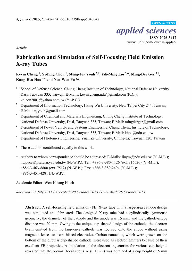
equations. First, the problem domain is divided into finite elements, as shown in Figure 1, and each
element is represented by a set of element equations to the original problem. To make the final
calculation, all element equations are systematically recombined into a global system of equations,
which can be numerically solved by known techniques from the initial values in the original problem.
Figure 1. X-ray tube divided into finite elements for electric field calculations. Red and
blue parts are anode and cathode, respectively.
The FEM is the preferred method in structural mechanical analysis. In this study, the FEM is a
suitable tool for obtaining a numerical solution for the spatial distribution of the electric field between
the cathode and the anode.
2.2. Field Emission Theory
FE refers to the quantum-mechanical phenomenon of electron tunneling from a conductor into
the vacuum through a surface potential barrier whose width is significantly reduced by a high local
electric field [21–25]. The tunneling probability depends very strongly on the width of the potential
barrier and decreases exponentially with increasing barrier width. The local electric field can be orders

Appl. Sci. 2015, 5 945
of magnitude greater than the applied macroscopic field, owing to the enhancement effect at sharp
tips or edges.
The FE current (I) can be calculated from the quantum-mechanical tunneling probability of electrons
through a triangular potential barrier, and the result is the well-known Fowler-Nordheim (F-N) equation:
2 2 3/2α (β / )exp( /β )I A E b E= φ − φ (1)
where α and b are constants; A is the effective FE area; E, ϕ, and β are the applied macroscopic electric
field (without the local microscopic geometrical effect that causes enhancement), the material work
function, and the field enhancement factor, respectively. The value of β depends on the microscopic
geometry of the emitters and is the most important factor that affects the FE performance.
Nanomaterials with enormously high aspect ratios, such as CNCs and CNTs, are known to have very
high β, and have been demonstrated to be excellent field emitters with low turn-on E fields [21–25].
The value of β can be extracted from the experimentally obtained slope of the F-N plot.
To obtain the macroscopic electric field E, which determines the FE current density, Poisson’s
equation was firstly solved numerically for the potential distribution V(x, y, z) using the FEM. The
electric field distribution is then calculated by differentiation:
E V= −∇
(2)
In this work, three different kinds of software packages were used in the simulation; they were
(1) SolidWorks® (Dassault Systèmes SolidWorks Corp., Waltham, MA, USA), which was used to
define a precise device geometry; (2) Comsol Multiphysics (Comsol Inc., Stockholm, Sweden), which
was used to calculate the distribution of the electric field on the designed cathode surface; and (3)
Simion 8.0 (Scientific Instrument Services, Inc., Ringoes, NJ, USA), which simulated the trajectory of
the emitted electrons that were accelerated by the electric field between the cathode and the anode.
2.3. CNCs as Electron Emitting Nanomaterial
The unique properties of carbon nanomaterials, such as their high thermal conductivity, low work
function, and excellent electron migration rate, make them promising FE emitters. CNTs have received
much attention since their discovery by Iijima [26–32]. An advantage of CNTs in FE is that they are
natural field-enhancing objects because of their high aspect ratio.
CNCs [13–16,33–37] are nanocarbon materials with a coiled structure and are composed of
nanometer-scale fibers. Compared with CNTs, CNCs have considerably more electron emission
sites—not only at the tips but also at the numerous nanocrystallites embedded in the amorphous carbon
body. Additionally, CNCs are more robust than CNTs because the former are much thicker and thus
can withstand a higher current density. Owing to their much larger diameter and higher FE site density,
CNCs exhibit better long-term current emission stability, current density, FE efficiency, and lifetime
than CNTs [18,19], and so they have already found application in FE lighting [38–41]. Consequently,
CNCs are used as the emitter material in the X-ray tube in this work.
CNCs are generally synthesized by catalytic thermal chemical vapor deposition (TCVD) or arc
discharge. Since CVD can be used in the low-cost, large-scale commercial synthesis of CNCs, it was
utilized to synthesize the CNCs herein.
Appl. Sci. 2015, 5 946
The substrates that were used herein for the synthesis of CNC cathodes were 304 stainless steel
circular disks with a diameter of 15 mm. Each substrate was firstly cleaned with acetone,
ultrasonicated for 10 min, and subsequently washed in deionized water. To expose the bare metal
surface, each stainless steel substrate was then immersed in 10%–37% HCl for 3–10 min and rinsed
again with deionized water. Before TCVD, Pd catalysts were deposited onto the substrates through
chemical displacement in a 100–800 ppm PdCl2 solution of pH 1.6–1.8 at 80 °C for 10 min. After the
reaction was complete, the cathodes were rinsed with deionized water and dried with N2 gas. The
prepared cathodes were placed in a TCVD furnace and the pressure was pumped down to 10−2 Torr.
The temperature was gradually increased to 600 °C at a rate of 20 °C/min in an atmosphere of H2 and
Ar. The flow rates for H2 and Ar were 10 and 100 sccm, respectively. When the temperature reached
600 °C, the Ar gas was evacuated and the H2 flow rate was increased to 20 sccm to pretreat the Pd
catalysts for 5 min. Next, to grow the CNCs, C2H2 gas was fed at a flow rate of 5 sccm for 20 min
while the furnace temperature was maintained at 600 °C.
The morphologies of the CNCs were examined using a transmission electron microscope (TEM,
model: Tecnai F30, FEI, Hillsboro, OR, USA) and a field emission scanning electron microscope
(FE-SEM, model: JEOL JSM-7600F, Japan Electron Optic Laboratory Co., Ltd., Tokyo, Japan). Their
graphite crystallinity was analyzed using Raman spectroscopy.
3. Results and Discussion
3.1. Simulation of the Self-Focusing Cathode Design
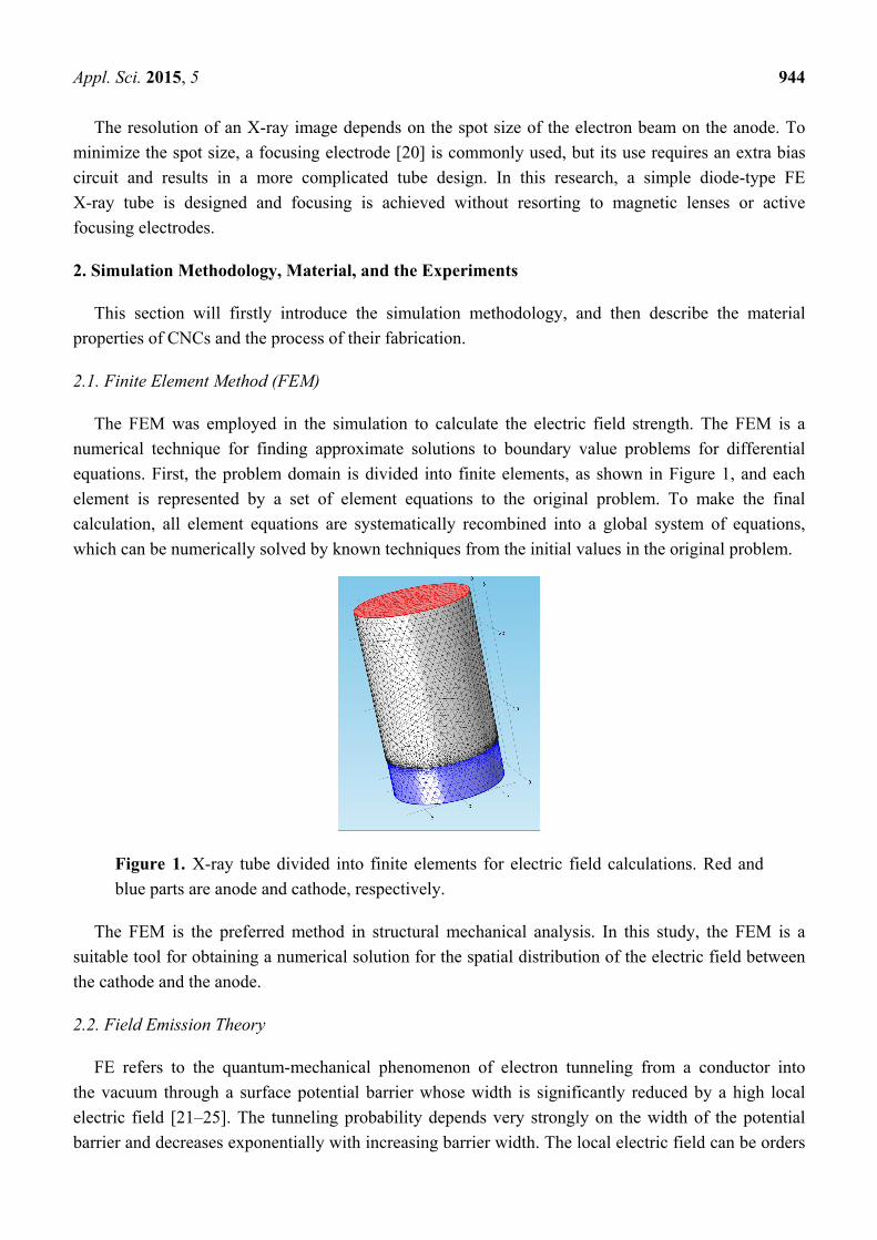
Figure 2 displays the geometry of the X-ray tube for simulation. The red part is the anode, which
has a diameter of 15 mm and is biased at an applied voltage of 50 kV; the blue part is the metallic cup
for electrostatic focusing which has a diameter of 15 mm with a 12-mm-diameter aperture on the top to
focus the emitted electrons. The CNC FE cathode disk (not shown) was situated at the bottom of
the metallic cup. The whole cathode (CNC FE disk and cup) was grounded. The distance from the
electron emitters to the anode was fixed at 20 mm, and the cup height was varied to minimize the size
of the focal spot on the anode.
Figure 2. Geometry of the X-ray tube in SolidWorks. Red and blue parts are anode and
cup-shaped cathode, respectively. CNC FE disk (diameter = 15 mm) is at the bottom
offocusing cup; a 12-mm-diameter aperture is at the top of cup.

Appl. Sci. 2015, 5 947
In the design herein, the electron-emitting area was quite large. This was advantageous because it
would greatly reduce the average current density if the total FE current was fixed, resulting in a longer
lifetime of the CNC emitters.
The electrostatic potential distribution and, hence, the electric field distribution were then calculated
using Comsol Multiphysics. Finally, the trajectories of the emitted electrons accelerated by the
Coulomb force were simulated using Simion 8.0. The calculated trajectories are shown in Figure 3.
(a) (b)
Figure 3. Trajectories of emitted electrons (a) without and (b) with focusing cup design.
Vertical axis in (b) represents electric potential V.
Figure 3a presents the simulation results for an X-ray tube without the focusing cup; electrons are
dragged by the applied voltage in straight trajectories to bombard the anode. In contrast, in Figure 3b,
the trajectories of the electrons emitted from a cup-shaped cathode clearly converged onto a small
focal spot. After testing with various heights of the cup-shaped cathode, the optimal cup height was
about 5 mm, which yielded the smallest focal spot size of 0.1 mm (diameter). Figure 4 shows the
three-dimensional (3D) electron trajectories in the X-ray tube with a 5-mm-high focusing cup.
Figure 4. Three-dimensional (3D) diagram of electron trajectories in the X-ray tube with a
5-mm-high focusing cup.
Note that the focusing cup is maintained at the same voltage as the CNC FE disk. Thus, no extra
bias circuit is needed, and the structure and fabrication of such an X-ray tube are simple.
Appl. Sci. 2015, 5 948
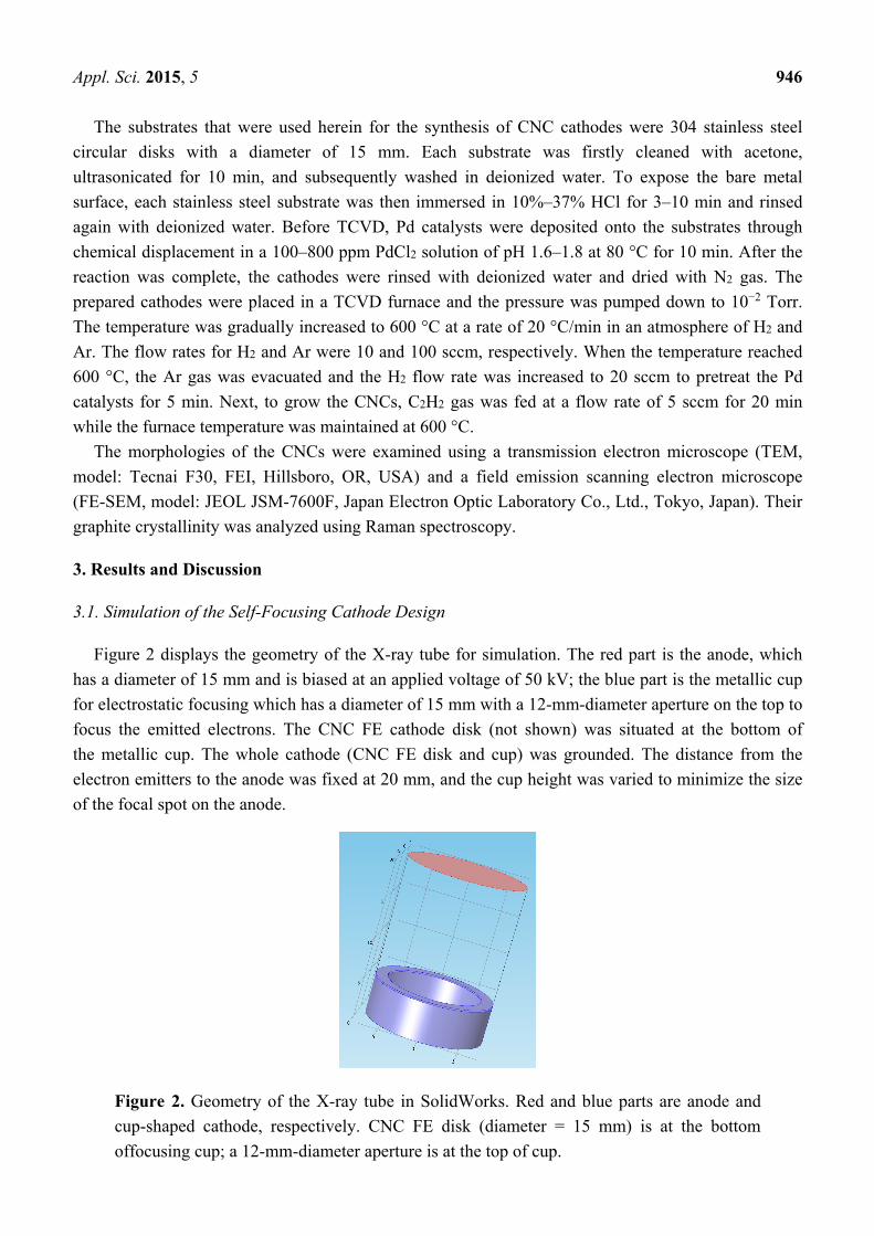
To understand why this simple design offered such a good focusing effect for a large-area cathode,
Figure 5 shows the electric field distribution on the CNC FE disk (a) without and (b) with the focusing
cup design. Comparing Figure 5a with b, the metallic cup wall clearly has a strong shielding effect:
the electric field strength near the disk edge was reduced from 9.5 × 10⁵ V/m (center) to below
1.2 × 10⁵ V/m. In contrast, the electric field without the focusing cup was nearly constant everywhere
on the CNC FE disk. This shielding effect forced the electric field lines within the cup to converge
towards the central axis, so the electrons were guided by this field distribution and focused onto
the anode.
(a) (b)
Figure 5. Calculated electric field strength on the surface of CNC FE disk (a) without and
(b) with focusing cup design.
3.2. Characterization of the Synthesized CNCs
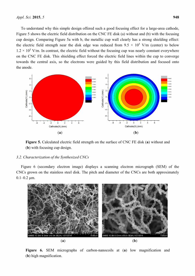
Figure 6 (secondary electron image) displays a scanning electron micrograph (SEM) of the
CNCs grown on the stainless steel disk. The pitch and diameter of the CNCs are both approximately
0.1–0.2 μm.
(a) (b)
Figure 6. SEM micrographs of carbon-nanocoils at (a) low magnification and
(b) high magnification.

Appl. Sci. 2015, 5 949
A TEM image of the CNCs synthesized at 600 °C is shown in the inset of Figure 7. The CNCs
synthesized at this temperature had a diameter of around 100 nm and an amorphous structure. A Pd
catalyst particle was observed in the micrograph (the red circle). Also shown in Figure 7 is the energy
dispersive X-ray (EDX) spectrum that was obtained within the red circle to reveal the chemical
composition of the catalyst particle (The Cu signal came from the Cu grid supporting the CNC samples
for TEM analysis).
Figure 7. TEM image of CNCs (inset) and EDX spectrum taken within the red circle,
which contained one Pd catalyst particle.
Figure 8 shows the Raman spectrum of the synthesized CNCs. The D-band at around 1350 cm−1 and
the G-band at 1580 cm−1 are clearly seen; they are related to the structural defects and the graphite
lattice, respectively, in carbonaceous materials. The intensity ratio ID/IG, which is an indicator of the
crystallinity of carbon materials, is 0.78. This number is similar to those obtained for the CNCs in
previous studies [39,42].
Figure 8. Raman spectrum of as-grown CNC film.
Appl. Sci. 2015, 5 950
3.3. Test of X-Ray Tube
To validate the device simulation herein, an X-ray tube with the designated geometry and
dimensions (a 20 mm cathode-anode separation; a 15 mm diameter; a 5 mm focusing cup height; and a
Cu anode) was constructed and tested. The focal spot size was estimated experimentally to be roughly
≤0.8 mm. The deviation from the optimal simulation result might be attributed to the slightly different
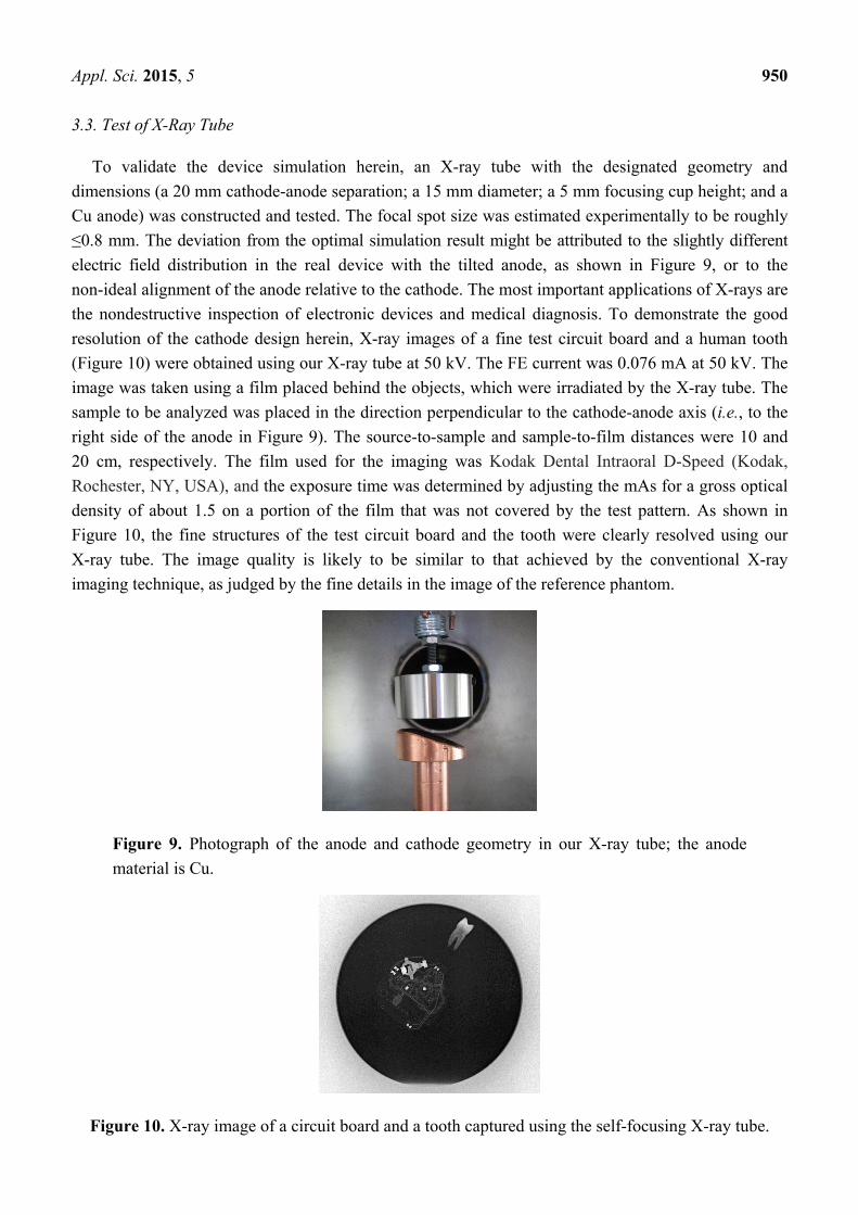
electric field distribution in the real device with the tilted anode, as shown in Figure 9, or to the
non-ideal alignment of the anode relative to the cathode. The most important applications of X-rays are
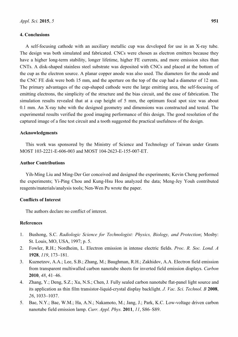
the nondestructive inspection of electronic devices and medical diagnosis. To demonstrate the good
resolution of the cathode design herein, X-ray images of a fine test circuit board and a human tooth
(Figure 10) were obtained using our X-ray tube at 50 kV. The FE current was 0.076 mA at 50 kV. The
image was taken using a film placed behind the objects, which were irradiated by the X-ray tube. The
sample to be analyzed was placed in the direction perpendicular to the cathode-anode axis (i.e., to the
right side of the anode in Figure 9). The source-to-sample and sample-to-film distances were 10 and
20 cm, respectively. The film used for the imaging was Kodak Dental Intraoral D-Speed (Kodak,
Rochester, NY, USA), and the exposure time was determined by adjusting the mAs for a gross optical
density of about 1.5 on a portion of the film that was not covered by the test pattern. As shown in
Figure 10, the fine structures of the test circuit board and the tooth were clearly resolved using our
X-ray tube. The image quality is likely to be similar to that achieved by the conventional X-ray
imaging technique, as judged by the fine details in the image of the reference phantom.
Figure 9. Photograph of the anode and cathode geometry in our X-ray tube; the anode
material is Cu.
Figure 10. X-ray image of a circuit board and a tooth captured using the self-focusing X-ray tube.
Appl. Sci. 2015, 5 951
4. Conclusions
A self-focusing cathode with an auxiliary metallic cup was developed for use in an X-ray tube.
The design was both simulated and fabricated. CNCs were chosen as electron emitters because they
have a higher long-term stability, longer lifetime, higher FE currents, and more emission sites than
CNTs. A disk-shaped stainless steel substrate was deposited with CNCs and placed at the bottom of
the cup as the electron source. A planar copper anode was also used. The diameters for the anode and
the CNC FE disk were both 15 mm, and the aperture on the top of the cup had a diameter of 12 mm.
The primary advantages of the cup-shaped cathode were the large emitting area, the self-focusing of
emitting electrons, the simplicity of the structure and the bias circuit, and the ease of fabrication. The
simulation results revealed that at a cup height of 5 mm, the optimum focal spot size was about
0.1 mm. An X-ray tube with the designed geometry and dimensions was constructed and tested. The
experimental results verified the good imaging performance of this design. The good resolution of the
captured image of a fine test circuit and a tooth suggested the practical usefulness of the design.
Acknowledgments
This work was sponsored by the Ministry of Science and Technology of Taiwan under Grants
MOST 103-2221-E-606-003 and MOST 104-2623-E-155-007-ET.
Author Contributions
Yih-Ming Liu and Ming-Der Ger conceived and designed the experiments; Kevin Cheng performed
the experiments; Yi-Ping Chou and Kung-Hsu Hou analyzed the data; Meng-Jey Youh contributed
reagents/materials/analysis tools; Nen-Wen Pu wrote the paper.
Conflicts of Interest
The authors declare no conflict of interest.
References
1. Bushong, S.C. Radiologic Science for Technologist: Physics, Biology, and Protection; Mosby:
St. Louis, MO, USA, 1997; p. 5.
2. Fowler, R.H.; Nordheim, L. Electron emission in intense electric fields. Proc. R. Soc. Lond. A
1928, 119, 173–181.
3. Kuznetzov, A.A.; Lee, S.B.; Zhang, M.; Baughman, R.H.; Zakhidov, A.A. Electron field emission
from transparent multiwalled carbon nanotube sheets for inverted field emission displays. Carbon
2010, 48, 41–46.
4. Zhang, Y.; Deng, S.Z.; Xu, N.S.; Chen, J. Fully sealed carbon nanotube flat-panel light source and
its application as thin film transistor-liquid-crystal display backlight. J. Vac. Sci. Technol. B 2008,
26, 1033–1037.
5. Bae, N.Y.; Bae, W.M.; Ha, A.N.; Nakamoto, M.; Jang, J.; Park, K.C. Low-voltage driven carbon
nanotube field emission lamp. Curr. Appl. Phys. 2011, 11, S86–S89.

Appl. Sci. 2015, 5 952
6. Wang, S.; Calderon, X.; Peng, R.; Schreiber, E.C.; Zhou, O.; Chang, S. A carbon nanotube field
emission multipixel X-ray array source for microradiotherapy application. Appl. Phys. Lett. 2011,
98, 213701.
7. Whitlock, R.R.; Bell, M.I.; Kerns, D.V.; Kerns, S.; Davidson, J.L.; Kang, W.P. Transmission
Cathode for X-ray Production. U.S. Patent 6,333,968, 25 December 2001.
8. Sugie, H.; Tanemura, M.; Filip, V.; Iwata, K.; Takahashi, K.; Okuyama, F. Carbon nanotubes as
electron source in an X-ray tube. Appl. Phys. Lett. 2001, 78, 2578–2580.
9. Bandaru, P.R. Electrical properties and applications of carbon nanotube structures. J. Nanosci.
Nanotechnol. 2007, 7, 1239–1267.
10. Zou, R.; Hu, J.; Song, Y.; Wang, N.; Chen, H.; Chen, H. Carbon nanotubes as field emitter.
J. Nanosci. Nanotechnol. 2010, 10, 7876–7896.
11. Sarada, Y.; Agarwal, S.; Kar, K.K. A Simple Method for Controlled Growth of Carbon Nanocoils
on Metallic Wire by Chemical Vapor Deposition. Nanosci. Nanotechnol. Lett. 2009, 1, 213–217.
12. Zhang, M.; Nakayama, Y.; Pan, L. Synthesis of carbon tubule nanocoils in high yield using
iron-coated indium tin oxide as catalyst. Jpn. J. Appl. Phys. 2000, 39, 1242–1244.
13. Chen, X.; Yang, S.; Motojima, S. Morphology and growth models of circular and flat carbon coils
obtained by the catalytic pyrolysis of acetylene. Mater. Lett. 2002, 57, 48–54.
14. Hernadi, K.; Fonseca, A.; Nagy, J.B.; Fudala, Á.; Bernaerts, D.; Kiricsi, I. Catalytic production of
carbon nanofibers over iron carbide doped with Sn2+. Appl. Catal. A 2002, 228, 103–113.
15. Chen, X.; Saito, T.; Kusunoki, M.; Motojima, S. Three-dimensional vapor growth mechanism of
carbon microcoils. J. Mater. Res. 1999, 14, 4329–4336.
16. Chen, X.; Motojima, S. The growth patterns and morphologies of carbon micro-coils produced by
chemical vapor deposition. Carbon 1999, 37, 1817–1823.
17. Liu, H.; Saito, Y. Influence of surface roughness on field emission of electrons from carbon
nanotube films. J. Nanosci. Nanotechnol. 2010, 10, 3983–3987.
18. Zhang, Z.; He, P.; Sun, Z.; Feng, T.; Chen, Y.; Li, H.; Tay, B. Growth and field emission property
of coiled carbon nanostructure using copper as catalyst. Appl. Surf. Sci. 2010, 256, 4417–4422.
19. Sung, W.Y.; Ok, J.G.; Kim, W.J.; Lee, S.M.; Yeon, S.C.; Lee, H.Y.; Kim, Y.H. Synthesis and
field emission characteristics of carbon nanocoils with a high aspect ratio supported by copper
micro-tips. Nanotechnology 2010, 18, 245603.
20. Zhang, J.; Cheng, Y.; Lee, Y.Z.; Gao, B.; Qiu, Q.; Lin, W.L.; Lalush, D.; Lu, J.P.; Zhou, O.
A nanotube-based field emission X-ray source for microcomputed Tomography. Rev. Sci.
Instrum. 2005, 76, 094301.
21. Cheng, Y.; Zhou, O. Electron field emission from carbon nanotubes. Physique 2003, 4,
1021–1033.
22. Murphy, E.L.; Good, R.H., Jr. Thermionic Emission, Field Emission, and the Transition Region.
Phys. Rev. 1956, 102, 1464–1473.
23. Dyke, W.P.; Dolan, W.W. Field emission. Adv. Electron. Electron. Phys. 1956, 8, 89–183.
24. Gadzuk, J.W.; Plummer, E.W. Field Emission Energy Distribution (FEED). Rev. Mod. Phys.
1973, 45, 487–548.
25. Gomer, R. Field emission, field ionization and field desorption. Surface Sci. 1994, 299–300,
129–152.

Appl. Sci. 2015, 5 953
26. De Heer, W.A.; Ugarte, D. Carbon onions produced by heat treatment of carbon soot and their
relation to the 217.5 nm interstellar absorption feature. Chem. Phys. Lett. 1993, 207, 480–486.
27. Fan, S. Self-oriented regular arrays of carbon nanotubes and their field emission properties.
Science 1999, 283, 512–514.
28. Rinzler, A.G.; Hafner, J.H.; Nikolaev, P.; Nordlander, P.; Colbert, D.T.; Smalley, R.E.; Lou, L.;
Kim, S.G.; Tomanek, D. Synthesis of Large Arrays of Well-Aligned Carbon Nanotubes on Glass.
Science 1995, 269, 1550–1553.
29. De Heer, W.A.; Châtelain, A.; Ugarte, D. A Carbon Nanotube Field-Emission Electron Source.
Science 1995, 270, 1179–1180.
30. Saito, Y.; Uemura, S. Field emission from carbon nanotubes and its application to electron
sources. Carbon 2000, 38, 169–182.
31. Bonard, J.M.; Croci, M.; Klinke, C.; Kurt, R.; Noury, O.; Weiss, N. Carbon nanotube films as
electron field emitters. Carbon 2002, 40, 1715–1728.
32. Huang, J.X.; Chen, J.; Deng, S.Z.; She, J.C.; Xu, N.S. Field-emission fluorescent lamp using
carbon nanotubes on a wire-type cold cathode and a reflecting anode. J. Vac. Sci. Technol. B
2008, doi:10.1116/1.2970144.
33. Downs, W.B.; Baker, R.T.K. Novel carbon fiber-carbon filament structures. Carbon 1991, 29,
1173–1179.
34. Motojima, S.; Kawaguchi, M.; Nozaki, K.; Iwanaga, H. Preparation of coiled carbon fibers by
catalytic pyrolysis of acetylene, and its morphology and extension characteristics. Carbon 1991,
29, 379–385.
35. Kawaguchi, M.; Nozaki, K.; Motojima, S.; Iwanaga, H. A growth mechanism of regularly coiled
carbon fibers through acetylene pyrolysis. J. Cryst. Growth 1992, 118, 309–313.
36. Chen, X.; Motojima, S. Morphologies of carbon micro-coils grown by chemical vapor deposition.
J. Mater. Sci. 1999, 34, 5519–5524.
37. Chesnokov, V.V.; Zaikovskii, V.I.; Buyanov, R.A. Symmetric twisted carbon filaments
formed from butadiene-1,3 on Ni-Cu/MgO-catalyst: Growth regularities and mechanism. J. Mol.
Catal. A 2000, 158, 267–270.
38. Pu, N.W.; Youh, M.J.; Chung, K.J.; Liu, Y.M.; Ger, M.D. Field emission lamps prepared with
dip-coated and nickel electroless plated carbon nanotube cathodes. J. Nanosci. Nanotechnol.
2015, 15, 5093–5098.
39. Chung, K.J.; Pu, N.W.; Youh, M.J.; Liu, Y.M.; Ger, M.D.; Cheng, K.; Jiang, J.C. Improvement of
Field-Emission-Lamp Characteristics Using Nitrogen-Doped Carbon Nanocoils. Diam. Relat.
Mater. 2015, 53, 1–10.
40. Chung, K.J.; Pu, N.W.; Youh, M.J.; Liu, Y.M.; Ger, M.D.; Huang W.K. Improvement of Lighting
Uniformity and Phosphor Life in Field Emission Lamps Using Carbon Nano-Coils. J. Nanomater.
2015, in press.
41. Chou, Y.P.; Pu, N.W.; Ger, M.D.; Chung, K.J.; Hou, K.H.; Liu, Y.M. Bulb-Shaped Field
Emission Lamps Using Carbon Nano-Coil Cathodes. J. Nanosci. Nanotechnol. 2012, 12,
8316–8322.

Appl. Sci. 2015, 5 954
42. Huang, W.K.; Chung, K.J.; Liu, Y.M.; Ger, M.D.; Pu, N.W.; Youh, M.J. Carbon Nanomaterials
Synthesized Using a Spray Pyrolysis Method. Vacuum 2015, 118, 94–99.
© 2015 by the authors; licensee MDPI, Basel, Switzerland. This article is an open access article
distributed under the terms and conditions of the Creative Commons Attribution license
(http://creativecommons.org/licenses/by/4.0/).