Embed Size (px)
Citation preview

Nano Today (2010) 5, 231—242
avai lab le at www.sc iencedi rec t .com
journa l homepage: www.e lsev ier .com/ locate /nanotoday
REVIEW
Controlling nanoscale morphology in polymerphotovoltaic devices
Joanna E. Slotaa,1, Ximin Hea,1, Wilhelm T.S. Hucka,b,c,∗
a The Nanoscience Centre, University of Cambridge, 11 J.J. Thomson Avenue, Cambridge CB3 0FF, United Kingdomb Melville Laboratory, Department of Chemistry, University of Cambridge, Lensfield Road, Cambridge CB2 1EW, United Kingdomc Radboud University Nijmegen, Institute for Molecules and Materials, Heyendaalseweg 135, 6525 AJ Nijmegen, The Netherlands
Received 3 March 2010; received in revised form 5 May 2010; accepted 6 May 2010
KEYWORDSPolymerphotovoltaics;Nanoscalemorphology;
Summary Whilst inspiring significant academic interest, the maximum power conversionefficiencies achieved by polymer PVs under solar conditions (PCE; 6.10—6.77%), are not yetsufficient for the devices to become widely marketable. Therefore much current work in thearea is focussed on raising device efficiencies as far as possible towards theoretically achievablelevels. To this end, key strategies involve material design and synthesis, device processing, and
Phase separation;Nanoimprintlithography
methods for controlling the morphology of the active components.This review aims to highlight the importance of morphological design and control for highly
efficient polymer PVs, to discuss strategies by which morphology can be controlled, and tooutline some of the characterisation techniques vital to the understanding and optimisation of
ials.ts re
shgS[
morphology in these mater© 2010 Elsevier Ltd. All righ
International discourse on climate change has beenemphasising the need for clean and renewable energy tech-nologies, to supersede fossil fuels and reduce the emissionof CO2. An estimated 120,000 TW of solar energy incidenton the surface of the Earth represents the largest source of
renewable energy available for such technologies. Althoughconventional silicon photovoltaics (PVs) have been an avail-able means of converting this solar energy into electricity for56 years [1], the high cost of single crystal Si, and expen-∗ Corresponding author at: Melville Laboratory, Department ofChemistry, University of Cambridge, Lensfield Road, Cambridge CB21EW, United Kingdom.
E-mail address: [email protected] (W.T.S. Huck).1 These authors contributed equally.
bteiemtpcp
1748-0132/$ — see front matter © 2010 Elsevier Ltd. All rights reserved.doi:10.1016/j.nantod.2010.05.004
served.
ive (high temperature and vacuum) production techniquesave inhibited their extensive use: even after considerablerowth and investment in recent years, PVs (90% of which arei) account for less than 1% of the world’s electric capacity2].
In order for PVs to become more prevalent and thusetter harness solar energy for human endeavour, new PVechnologies are being developed to allow reduced costs ornhanced efficiency [3]. One such promising area of researchs polymer PV devices, in which the thin film active lay-rs comprise either: polymers only, polymer—small molecule
ixtures, or polymer—inorganic hybrids. Polymer PVs holdhe potential to become more commonplace as energyroviders than their inorganic counterparts, due to theirompatibility with inexpensive, low-temperature solutionrocessing and continuous deposition. There are also several

2
fro
iPstcclal
ltavimmwba
Dr
Amtcateepcsiwbfbaa
pa(teista
A
Ti
ara[bh
E
TiisltwfdpwtLd
dmoaainatL[tbwbrlfattL
mfb(ctTms
32
urther advantages associated with utilising polymeric mate-ials, such as their light weight, flexibility, and the possibilityf fine-tuning properties through organic synthesis.
Whilst inspiring significant academic interest, the max-mum power conversion efficiencies achieved by polymerVs under solar conditions (PCEs) (which approach, or inome reports exceed 7%) [4—7] are not yet sufficient forhe devices to become widely marketable. Therefore muchurrent work in the area is focussed on raising device effi-iencies as far as possible towards theoretically achievableevels [8]. To this end, key strategies involve material designnd synthesis, device processing, and methods for control-ing the morphology of the active components.
This review aims to highlight the importance of morpho-ogical design and control for highly efficient polymer PVs,o discuss strategies by which morphology can be controlled,nd to outline some of the characterisation techniquesital to the understanding and optimisation of morphologyn these materials. The discussion of morphology includesaterial shape, size, phase structuring and texture. Sinceolecular packing and crystallinity is intimately associatedith the material texture, discussion of the relationshipetween these factors and device performance is occasion-lly included.
evice operation and ideal morphologyequirements
lthough single-component polymer PVs are possible, theost successful devices are based on polymer heterojunc-
ions [9]. This type of device incorporates two distinctomponents: the electron-accepting (acceptor), and hole-ccepting (donor) materials. The absorbing material (usuallyhe acceptor) has a bandgap in the visible region,nabling the absorption of photons to form bound, excitedlectron—hole pairs (Frenkel-type excitons). In order forhotocurrent to be generated, these excitons must be suc-essfully dissociated into free charge carriers, which mustubsequently migrate to the electrodes. High exciton bind-ng energies (∼0.3—0.5 eV) must be overcome, contrastingith the case for inorganic semiconductors, where such highinding energies are not seen and photoexcitation producesree charges under ambient conditions. As will be discussedelow, each step in the processes of current generation iscutely affected by the structure and composition of thective organic components.
In terms of the parameters normally used to quantify PVerformance [10], the overall efficiency of current gener-ted per incident photon, or external quantum efficiency�EQE) is the product of the efficiency of each step (absorp-ion, exciton diffusion, charge transfer, charge collection),ach of which is influenced by morphology. Morphologicalnfluence on light absorption and exciton diffusion influenceshort circuit current (Jsc); morphological influence on chargeransfer and collection affect the open circuit voltage (Voc),nd fill factor (FF).
bsorption
he efficiency of light absorption and exciton generations mainly contingent on the bandgap and thickness of the
ilomt
J.E. Slota et al.
bsorbing material. Semiconducting polymers can displayelatively high absorption coefficients (∼105 cm−1), whichllow efficient absorption within thin (100—200 nm) films11]. The absorption cross-sections can also be influencedy molecular environment and packing; polymer crystallinityas been shown enhance optical absorption [12,13].
xciton dissociation
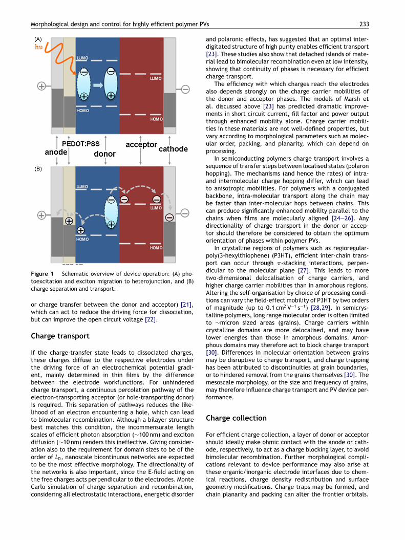
he driving force for exciton dissociation is imposed at thenterface between the donor and acceptor components,n the form of an electric field originating from an off-et between the donor and acceptor frontier orbital energyevels. Therefore the first step towards efficient dissocia-ion necessitates the random diffusion of neutral excitonsithin the material in which they are formed, to the inter-
ace, before relaxation to the ground state occurs. A largeonor/acceptor interface is therefore required such that allarts of the material, in which excitons are formed, areithin the exciton diffusion length (LD, average distance
ravelled before recombination), from the interface. TheD is specific to material, and depends on both the excitoniffusion coefficient, D and lifetime, �. LD = (D�)1/2.
Efficient polymer PVs will therefore have donor/acceptoromain sizes limited to the order of LD, with exact require-ents varying according to the material system. For many
rganic materials based on coplanar hydrocarbons, excitonsre primarily in the first excited singlet (S1) state, withn approximately nanosecond lifetime, bringing about LD
n the order of ∼10 nm. For materials including heavier,on-coplanar components such as C60, spin—orbit couplingllows significant cross-over to the triplet (T1) state. Sincehe T1 state displays an approximately microsecond lifetime,D may be longer (several 10 s of nm) for these materials14,15]. Although a complete theoretical understanding ofhe mechanisms by which S1 and T1 excitons diffuse has noteen obtained, morphology (specifically, molecular packinghich can alter intermolecular interactions) is thought toe a controlling factor. For example, molecular orderingeduces Stokes shift, leading to a better spectral over-ap between emission and absorption, which is favourableor Förster transitions, by which singlet excitons are oftenpproximated to diffuse [16]. It is also noted that sinceriplet excitons are considered to diffuse by slower, Dexterransfer they may not necessarily lead to a greatly increasedD [17] (Fig. 1).
Once an exciton reaches the donor/acceptor interface,ore weakly bound charge-transfer (CT) states may be
ormed. These polar pairs may recombine (geminate recom-ination), recombine with charges on adjacent moleculesbimolecular recombination), or dissociate via a series ofharge separated (CS) states to generate a mobile elec-ron and hole in the acceptor and donor, respectively.he relative probabilities of recombination and dissociationay depend on the morphology at the interface. Tran-
ient absorption experiments provide evidence of a decrease
n geminate pair recombination with increased molecu-ar order [18,19], although varying explanations have beenffered as to the mechanism for this improvement [20]. Theolecular packing configuration may enhance a dipole athe interface (sometimes formed from specific polarization
Morphological design and control for highly efficient polymer PV
ad[rsc
atamttvup
shatbbccdto
ppdthAtottclp[mhommf
C
Fsob
Figure 1 Schematic overview of device operation: (A) pho-toexcitation and exciton migration to heterojunction, and (B)charge separation and transport.
or charge transfer between the donor and acceptor) [21],which can act to reduce the driving force for dissociation,but can improve the open circuit voltage [22].
Charge transport
If the charge-transfer state leads to dissociated charges,these charges diffuse to the respective electrodes underthe driving force of an electrochemical potential gradi-ent, mainly determined in thin films by the differencebetween the electrode workfunctions. For unhinderedcharge transport, a continuous percolation pathway of theelectron-transporting acceptor (or hole-transporting donor)is required. This separation of pathways reduces the like-lihood of an electron encountering a hole, which can leadto bimolecular recombination. Although a bilayer structurebest matches this condition, the incommensurate lengthscales of efficient photon absorption (∼100 nm) and excitondiffusion (∼10 nm) renders this ineffective. Giving consider-ation also to the requirement for domain sizes to be of theorder of LD, nanoscale bicontinuous networks are expected
to be the most effective morphology. The directionality ofthe networks is also important, since the E-field acting onthe free charges acts perpendicular to the electrodes. MonteCarlo simulation of charge separation and recombination,considering all electrostatic interactions, energetic disorderctigc
s 233
nd polaronic effects, has suggested that an optimal inter-igitated structure of high purity enables efficient transport23]. These studies also show that detached islands of mate-ial lead to bimolecular recombination even at low intensity,howing that continuity of phases is necessary for efficientharge transport.
The efficiency with which charges reach the electrodeslso depends strongly on the charge carrier mobilities ofhe donor and acceptor phases. The models of Marsh etl. discussed above [23] has predicted dramatic improve-ents in short circuit current, fill factor and power output
hrough enhanced mobility alone. Charge carrier mobili-ies in these materials are not well-defined properties, butary according to morphological parameters such as molec-lar order, packing, and planarity, which can depend onrocessing.
In semiconducting polymers charge transport involves aequence of transfer steps between localised states (polaronopping). The mechanisms (and hence the rates) of intra-nd intermolecular charge hopping differ, which can leado anisotropic mobilities. For polymers with a conjugatedackbone, intra-molecular transport along the chain maye faster than inter-molecular hops between chains. Thisan produce significantly enhanced mobility parallel to thehains when films are molecularly aligned [24—26]. Anyirectionality of charge transport in the donor or accep-or should therefore be considered to obtain the optimumrientation of phases within polymer PVs.
In crystalline regions of polymers such as regioregular-oly(3-hexylthiophene) (P3HT), efficient inter-chain trans-ort can occur through �-stacking interactions, perpen-icular to the molecular plane [27]. This leads to morewo-dimensional delocalisation of charge carriers, andigher charge carrier mobilities than in amorphous regions.ltering the self-organisation by choice of processing condi-ions can vary the field-effect mobility of P3HT by two ordersf magnitude (up to 0.1 cm2 V−1 s−1) [28,29]. In semicrys-alline polymers, long range molecular order is often limitedo ∼micron sized areas (grains). Charge carriers withinrystalline domains are more delocalised, and may haveower energies than those in amorphous domains. Amor-hous domains may therefore act to block charge transport30]. Differences in molecular orientation between grainsay be disruptive to charge transport, and charge trapping
as been attributed to discontinuities at grain boundaries,r to hindered removal from the grains themselves [30]. Theesoscale morphology, or the size and frequency of grains,ay therefore influence charge transport and PV device per-
ormance.
harge collection
or efficient charge collection, a layer of donor or acceptorhould ideally make ohmic contact with the anode or cath-de, respectively, to act as a charge blocking layer, to avoidimolecular recombination. Further morphological compli-
ations relevant to device performance may also arise athese organic/inorganic electrode interfaces due to chem-cal reactions, charge density redistribution and surfaceeometry modifications. Charge traps may be formed, andhain planarity and packing can alter the frontier orbitals.
234 J.E. Slota et al.
Figure 2 Illustration of the ideal interdigitated architecturewithin the active layer of polymer PVs, summarising the mainmorphological considerations. This includes nanoscale phasedimensions (with the exact size determined by LD), chargeblocking layers at each electrode, and a compromise in thick-ness such that the absorbing layer is thick enough for efficientabsorption of incident light, but thin enough to allow excitondiffusion to the heterojunction and charge transport to the elec-trodes. Not shown is the ideal molecular order (which in generalaids both exciton, and free charge carrier transport). Struc-tti
StcPpeihity(
M
C[miiaalrdnta
iPghonp
Ftp
attrtw(
M
Cccitrsmttaoetpdetesatas
pmdmlm(bb
ural requirements at the donor/acceptor interface, as well ashe interfaces with each electrode, are complicated but alsomportant.
urface treatments such as plasma oxidation of ITO elec-rodes, or self-assembled monolayers have been used to helpompatibility, reducing traps and enhancing contact [31].oly(ethylene-dioxythiophene) doped with poly(styrene sul-honic acid) (PEDOT·PSS) is generally used as polymerlectrode (coating the transparent inorganic electrode), tomprove the surface contact, reduce shorts, and facilitateole extraction. Extensive work on modeling and character-sation of the morphology-dependent electronic structure athe organic—organic and organic—metal interfaces has notet led to a comprehensive predictive understanding [32,33]Fig. 2).
ethods towards controlled morphology
onventionally, the bulk heterojunction device structure34—36] has been used to approximate the morphologyost favourable for efficient polymer PVs, whilst utiliz-
ng a beguilingly simple fabrication process. This processnvolves casting a mixture of donor and acceptor, usu-lly from solution, forming a blended film. The resultingrchitecture is composed of randomly orientated phases atengthscales natural to the phase separation of the mate-ials (mainly dependent on Flory-Huggins parameters). Theonor/acceptor interface is large, and for several combi-ations of materials, phases are spontaneously produced athe appropriate lengthscale to afford exciton dissociation,s can be shown by PL quenching [34].
Although the simplicity and affordability of fabrications, as we have discussed, key to the potential of polymerVs, bulk heterojunctions only partially fulfil the strin-
ent morphological conditions for efficient devices, andave therefore exhibited limited efficiencies. The morphol-gy may be approximated to bicontinuous interpenetratingetworks, but the phases often do not comprise pure com-onents, which has a complex effect on charge transportwmtcf
igure 3 Illustration of the bulk heterojunction device struc-ure, typically arising from spincasting blends and arrestinghase separation.
nd may lead to increased recombination. There is no wayo control the percolation path of each material to the elec-rodes, and unconnected islands are likely. Phases are alsoandomly aligned with respect to electric field. Connectivityo electrodes is hard to control, and wetting the electrodesith the inappropriate polymer cannot easily be avoided
Fig. 3).
aterial design
onsiderable synthetic endeavour has been engaged inhemically tuning the properties of polymers for PV appli-ations [4—6,37—41]. The palette of materials successfuln bulk heterojunction PVs has been limited not only byheir optoelectronic properties, but also their phase sepa-ation behaviour. Polymer regioregularity, molecular weight,ide chains, and polydispersity tend to be tailored to opti-ise absorption and electronic properties such as charge
ransport, but also have a strong impact on solubility andhe morphology of cast blends [6,42,43]. Chemical alter-tions aimed at enhancing morphology may similarly impactptoelectronic properties. For example, side groups maynhance solubility (which can enable more uniform, con-rolled morphology), but interfere with mobility and opticalroperties by disrupting molecular order by steric hin-rance, chain-twisting, or altering the HOMO energy bylectron donation [43—46]. Since morphology and optoelec-ronic properties are intertwined, screening for the mostffective PV materials is complicated. Success is limitedince the multitude of required properties (an appropri-te bandgap for absorption, an offset in frontier orbitalso promote exciton diffusion, good charge carrier mobilitynd the ability to spontaneously phase separate into idealtructures), cannot be simultaneously optimised.
The most successful materials currently available forolymer PVs are blends of conjugated polymer withethanofullerene small-molecules in bulk heterojunctionevices [4—6]. Although these show promising device perfor-ances, the control and understanding of the morphology is
imited; nanoscale phase separation shown in atomic forceicroscopy (AFM) and transmission electron microscopy
TEM) imaging is not well defined. In the systems studiedy Chen et al. [4], the bulk heterojunction with least visi-le molecular organisation showed the highest performance,
hereas for Park et al. [5], ordered PCDTBT [40] fibrils wereost visible in the most efficient devices. The successes ofhese investigations lead to further questions about how theontrol of morphology, in these, and similar materials mayurther enhance device performance.

r PV
P
Ahotttdiuipmgtcwi
rfcispaiF
aepb2srzaiomarAtPadPLidrtsa
Morphological design and control for highly efficient polyme
Processing conditions
The morphologies of bulk heterojunction films cast fromblends are generally only kinetically stable, and sensitiveto many parameters during processing. Altering the uniquebalance of kinetic control and thermodynamic influencesin each system can be used to manipulate the size andconnectivity of demixed phases [47]. Conditions such asconcentration [48,49], ratio of materials [5,49,50], solventtype [5,49,51—54], solvent mixtures (including additivesno longer detected after processing) [4,6,7,55—58], cast-ing speed, solvent evaporation rate [59,60], temperature,humidity, and substrate wetting interactions [61] haveall been used to optimise bulk heterojunction morphol-ogy. For example, an empirically optimised PCDTBT:PC70BMratio of 1:4 has recently been used to achieve high PCEs(∼6%). Increasing the relative amount of PC70BM througha series of blends seemingly induced the formation ofbetter connected pathways of PCDTBT fibrils, produc-ing enhanced fill factors [5]. Mechanisms and detaileddiscussions of these material-dependent thermodynamicinfluences have been discussed in several review articles[47,62,63,67].
Domain size and connectivity has been successfullymanipulated in a number of studies by the inclusion of pro-cessing additives. In recent work by Liang et al. [6] a range ofpolymers based on thieno[3,4-b]thiophene and benzodithio-phene units were blended with the fullerene derivative[6,6]-phenyl-C61-butyric acid methyl ester (PC61BM). Thepolymer with most favourable mobility and HOMO energylevel of the studied set was seen to phase separate read-ily from PC61BM in 1,2-dichlorobenzene, producing phasesover 100 nm and low PCE (3.10%). Processing from a mixedsolvent including 3% 1,8-diiodooctane was implemented toimprove the morphology (reduce the domain sizes), andobtain a PCE over 6%. Morphology control using the sameadditive has enabled some of the highest PCEs ever reportedin the field (up to 7.4%) [4,7]. Lee et al. have suggested thatthese additives function through selective solubility for oneblend material, and having a higher boiling point than thebulk solvent, which leads to enhanced separation of phasesin the liquid state, and slower drying of one component[58].
Some evidence has suggested that specific process-ing conditions can induce vertical segregation within theblends, which can enhance PV efficiency when the donoror acceptor-rich regions are suitably orientated relative tothe electrodes. XPS studies showed slight vertical strat-ification of P3HT and PC61BM when a 1,8-octanedithiolsolvent additive was used [57]. Changing surface wettinginteractions using alkyltrichlorosiliane surface treatmentand a viscous solvent has also produced vertical phaseseparation and enhanced �EQE in polyfluorene blends[61].
Altogether, few general rules apply to the optimisationof each specific bulkheterojunction fabrication process, andsome phenomena (such as the significant impact of adding
very low percentages of a secondary solvent) [4,6] are notpredictable. The processing conditions must be painstak-ingly tailored for each new material system; optimisationaffords only limited control, and blend morphologies remainnotoriously irreproducible.i
ato
s 235
ost-processing treatments
lthough the thermodynamic instability of blended bulketerojunction films represents a challenge to stable PVperation, it also offers a route improved morphologieshrough post-processing treatments. Thermal annealing hashe effect of allowing the morphology to equilibrate towardshe most energetically favourable configuration (often aemixed state). This means that domains often ripen andncrease in sizes. Although eventually this may lead tonfavourable domain sizes (�LD) [48], incomplete ripen-ng may enhance connectivity between phases and improveercolation pathways [64]. Equilibration in this manneray allow crystallinity to develop, which can be seen to
reatly enhance device performance in P3HT:PC61BM sys-ems; PC61BM is excluded from P3HT, and both phasesrystallise and form a nanoscale interpenetrating network,ith enhanced optical absorption and charge carrier mobil-
ties [65—67].Thermal annealing may also improve morphology by
emoving residual solvent, reducing trapping sites at inter-aces, or simply the smoothing the film to allow enhancedontact with the electrodes [59]. Thermal treatment maynduce vertical diffusion and segregation of materials; initu ellipsometry studies by Campoy-Quilles et al. showedreferred segregation of donor towards anode interfacend acceptor towards cathode interface during thermallynduced self-organisation and morphology evolution (seeig. 4) [68].
Equilibration in saturated solvent atmosphere (solventnnealing) has also been applied to modify bulk het-rojunction morphologies after casting. Solvent moleculesenetrate and solvate the film, allowing polymer chains toecome more mobile and facilitating self-organisation. In007 Zhao et al. reported that treatment with an atmo-phere of 1,2-dichlorobenzene improved the performance ofegioregular-P3HT/PC61BM blend PVs (spun from chloroben-ene) to an extent not achievable by thermal annealinglone [69]. AFM roughness analysis and strong vibronic bandsn the absorption spectra indicated that P3HT molecularrder had been more efficiently induced than when ther-al treatment was applied. Improved device performance
fter solvent annealing was attributed to the enhanceded-shifted absorption and improved hole mobility of P3HT.n additional thermal annealing step was found to fur-her improve the phase separated networks by promotingCBM aggregation. A combination of solvent and thermalnnealing techniques therefore produced the most efficientevices (PCE 3.7%). However, similar results and a higherCE (4.4%) had already been reported for the same blend byi et al., who had effectively introduced a solvent anneal-ng step, by slowing the evaporation of 1,2-dichlorobenzeneuring casting [59]. Later Chu et al. also achieved similaresults and a PCE of 3.8% for P3HT/PC71BM PVs from 1,2,4-richlorobenzene [70]. In both these studies, an insufficientpincoating time was used for the films to dry completely,nd equilibration was facilitated in the presence of remain-
ng solvent, in an enclosed environment.A further post-processing, cross-linking step has beenttempted in order to hinder diffusion and aggrega-ion within bulk heterojunction active layers. Segregationf PC61BM has been suppressed by utilising fullerene

236 J.E. Slota et al.
Figure 4 Vertical composition in P3HT:PCBM films as deduced using ellipsometry. PCBM vertical concentration profiles: (A) before(blue) and after (red) thermal annealing; (B) after spin coated at 5000 r.p.m. (blue), 3000 r.p.m. (green) or 700 r.p.m. (red); (C)b ateda Schea ith p
ocM(apldtid
B
Bttmadaso
tfiachoibm
attFpso
o
efore (blue) and after (red) vapour annealing; (D) after spin cohydrophobic self-assembled hexamethyldisilazane monolayer.nd (F) after vapour or thermal annealing. Image reproduced w
r polythiophene derivatives synthesised to incorporateross-linking functionality [71—73]. Investigating the latter,iyanishi et al. synthesised poly(3-(5-hexenyl)-thiophene)
P3HNT) which was blended with PC61BM then cross-linkedt the vinyl side chains to form a morphologically robustolymer PV [73]. Although the initial PCE was slightlyower than the equivalent non-cross-linked P3HT:PC61BMevice (3.16% as opposed to 3.33%), morphology was morehermally stable after cross-linking, and after 10 h anneal-ng PCE was much less deteriorated in the cross-linkedevice.
lock copolymers
lock copolymers are macromolecules consisting of morehan one type of repeat unit, organised into discrete sec-ions, or blocks along the chain. If the blocks compriseaterials which naturally phase separate, covalent link-
ges between the blocks limit the scale of phase separatedomains. Classical block copolymers spontaneously self-ssemble into a variety of periodic, ordered nanoscaletructures. The thermodynamic driving forces for suchrganisation are well understood; hence the manipula-
Sweas
on substrates with (right), or without (left) pretreatment withmatic representations of typical PCBM distributions: (E) beforeermission from Ref. [68].
ion of parameters such as relative block length andlm thickness can produce directed ordering [74]. Thespiration of exploiting block copolymer self-assembly toontrol nanoscale morphology in polymer PV applicationsas inspired much research over recent years. Enhancementf morphology in the active layer has been sought by util-sing block copolymers with optoelectronic functionality, ory using block copolymers to direct, or template desiredorphologies [75,76].In the ideal case, copolymers comprising donor and
cceptor blocks would spontaneously self-organise into con-inuous lamellae, or cylindrical structures perpendicular tohe electrodes, resembling the ideal morphology depicted inig. 2. Through simple processing, high purity charge trans-ort pathways would be formed, and the thermodynamicallytable morphology would endure elevated temperatures andperation conditions.
However, several problems have hindered the realisationf such systems described above in efficient polymer PVs.
emiconducting polymers often have conjugated backbones,hich introduce rigidity meaning that the thermodynamicquilibrium structures (determined by mixing interactionsnd molecular conformations) are distinct from those under-tood for classical coil block copolymers. Phase separation
Morphological design and control for highly efficient polymer PVs 237
plicam Re
ptbdbaas[dp
A
Tebtrsefidt[
isgogd[
Figure 5 (A) Schematic representation of an inverse gyroid regyroid array replicated in TiO2. Reproduced with permission fro
and self-assembly may also be hindered by bulky groupssuch as fullerenes [77]. Synthesis of rigid ‘‘rod’’ conju-gated block copolymers can also be arduous; there havebeen few reports of ‘‘rod—rod’’ copolymers, with little evi-dence of ordered self-assembly [78,79]. Flexibility can beintroduced into semiconducting polymers by including func-tional, conjugated moieties as pendant groups along thechain. Attention has focused on optoelectronic copolymerswith one flexible chain (‘‘rod—coil’’) [80—83], or two flexi-ble chains (‘‘coil—coil’’) [84,85], where periodic nanoscalemorphologies are more readily formed (such as lamellaeor hexagonal packed rods of (alkoxyphenylenevinylene-b-isoprene) [81,82], or fibrils of P3HT [83]). The mostsuccessful single-component block copolymer PVs have uti-lized ‘‘rod—coil’’ copolymers of P3HT and polyacrylateadorned with perylene bisimide pendants [86—88]. Thesehave shown good crystallinity in both phases, high pho-toluminescence quenching, �EQE and PCEs of up to 31%and 0.49%, respectively. These results are promising sincethe copolymer devices show improvement relative to theequivalent homopolymer blends, but efficiencies lag behindsimple blended devices in other materials.
Where optoelectronic functionality and spontaneous self-assembly have proved difficult to simultaneously achieve,alternative approaches involve templating or back-fillingfrom ordered block copolymer nanostructures [89,90]. Forexample, copolymers of poly(3-dodecylthiophene) (P3DDT)and insulating polylactide (PLA) have been synthesised.Selective chemical etching of PLA resulted in a porous,highly ordered film of P3DDT, which could be backfilled withmaterials such as PCBM for PV applications [89]. Tailoringthe relative volume fractions of poly(4-fluorostyrene) (PFS)and PLA blocks leads to the formation of a bicontinuous dou-ble gyroid phase [90]. Templating this morphology for use in
PVs has the advantage of obviating the need for alignment ofthe blocks, as direct pathways are present in every direction(see Fig. 5).Block copolymers could otherwise be introduced intohomopolymer blends to aid compatibility between disparate
wPpc
ted from block copolymer templates. (B) SEM of a ∼4 �m thickf. [90].
hases. Naturally acting at the interface, due to their struc-ural duality, they are thought to reduce interfacial tensionetween blend components, which stabilises nanoscaleomain sizes. Ripening was inhibited in P3HT:PC61BM blendsy the addition of 17 wt% of a copolymer containing P3HTnd C60; this significantly reduced the attenuation of PCEfter extended thermal treatment [91]. Block copolymerurfactants similar to those reported by the Thelakkat group88] have improved the PCE of P3HT:perylene tetracarboxy-iimide blend PVs (from 0.37% to 0.55%) by suppressinghase separation [92].
lignment and structuring techniques
o assist ordered assembly in polymer PV active lay-rs, top-down alignment or lithographic techniques maye employed. Alignment of polymers can been achievedhrough mechanical alignment (such as flow coating orubbing), Langmuir Blodgett deposition, liquid crystallineelf-organisation, alignment-directing substrates, which cannhance charge transport [24,25,93]. Coupling of a magneticeld to the diamagnetic moment of rod blocks can be used toirect self-assembly of amphiphillic block copolymers, buthis method has met with limited success for PV active layers94].
Soft lithographic techniques such as micro-contact print-ng or dip-pen nanolithography have been used to createurfaces patterned with regions of different surface ener-ies. These patterns can guide or force the phase separationf polymer blends into rather well-controlled morpholo-ies (see Fig. 6). However these techniques have only beenemonstrated at lengthscales exceeding LD in most polymers95—97].
Synthesising optoelectronic polymer brushes is anotheray of ensuring alignment and enhanced mobility in polymerVs (see Fig. 7) [26,98]. Recent breakthroughs in syntheticrocedures have enabled the growth of polymer brushesontaining conjugated polymer backbones, providing a first

238 J.E. Slota et al.
Figure 6 (A) Surface patterning method used to generate C60 patterns. An amine-terminated fullerene is introduced onto a surfacepatterned with mercaptohexadecanoic acid (MHA) by micro-contact printing or dip-pen nanolithography. The rest of the surface isbackfilled with alkanethiol. (B) AFM topography and (C) fluorescence microscopy of structured poly-[2-(3,7-dimethyloctyloxy)-5-methoxy-p-phenylenevinylene] (MDMO-PPV):PC61BM films prepared on C60/MHA patterned substrates. Vertical scale: 200 nm.Reproduced with permission from Ref. [95].
Figure 7 (A) AFM phase image of a 45 nm poly-(triphenylamine acrylate) (PTPAA) brush film grown from a glass substrate infiltratedwith 2.6 nm diameter CdSe nanocrystals. (B) Cartoon of inferred structure for CdSe nanocrystal infiltrated polymer brush photovoltaicdevice. From bottom to top: ITO-coated glass slide modified by surface attachment of a bromine end-caped trichlorosilane self-a ownb planc
sd
N
Nbcmdobuti(paTi
fiN
tosv(eiibdabr
ssembled-monolayer (SAM) (blue squares), polymer brushes grrush network exhibiting some degree of phase separation in theathode. Reproduced with permission from Ref. [98].
tep towards ‘synthesised’ rather than fabricated polymerevices [99].
anoimprint lithography
anoimprint lithography (NIL) is a hot embossing methody which large areas and high densities of nanostructuresan be simply replicated in polymers, from pre-patternedoulds. NIL is being investigated as a method for pro-ucing optimised morphologies in polymer PVs, since notnly can continuous phases with nanoscale patterninge rapidly formed, but a significant degree of molec-lar alignment may be simultaneously induced withinhese phases. Grazing incidence X-ray diffraction stud-es on regioregular-P3HT imprinted with a Si mould
treated with an anti-adhesion monolayer of 1H,1H,2H,2H-erfluorodecyltrichlorosilane (FDTS)) showed vertical chainlignment within ∼100 nm wide gratings and pillars [100].his alignment within the structures, summarised in Fig. 8,s thought to be determined by the geometry of nanocon-
mPbd
from the SAM (red lines), CdSe nanocrystals infiltrated into thee of the film (small black circles), and caped with an aluminum
nement, and surface interactions with the mould duringIL.
A handful of examples exist where ordered heterojunc-ion polymer PVs have been produced by the NIL patterningf an organic donor. Fullerene acceptor materials wereubseqently deposited by spincoating from a selective sol-ent [101,102], or evaporation [103,104]. The residual layernormally retained between features patterned by NIL)nsured complete contact of donor with the anode. Increas-ng the donor/acceptor surface area through NIL patterningmproved the Jscs, and the PCEs by up to five times relative toilayer devices [103]. However, the dimension of imprintedomains was much larger than the exciton diffusion lengths,nd PCEs were limited. The highest PCE of 2.5% was achievedy 2D patterned P3HT:PCBM, which is far lower than the besteports for bulk heterojunctions of the same system [102].
Recently, smaller NIL masters and a double-imprintethodology achieved an ordered heterojunction polymerV with greater PCE than the equivalent optimised blendedulkheterojunction [105]. P3HT was patterned with highensity arrays of nanostructures by solvent-assisted NIL,

Morphological design and control for highly efficient polymer PVs 239
Figure 8 Illustrations of the effect of NIL on P3HT molecular alignment, determined by grazing incident X-ray diffraction. (A)tionating
Mechanism of chain alignment due to polymer flow and interacsurface. Schematics of ideal P3HT chain alignment in (B) nanogrRef. [100].
and thermally annealed before demoulding to improve crys-tallinity. The resulting P3HT nanostructures were stampedinto a heated film of F8TBT acceptor material, in a secondNIL process. The result was a precisely defined interdigi-
tltr
Figure 9 (A) Schematic procedure of double imprinted PV devicelow intensity �EQE and PCE. (C) SEM images of imprinted 80 nm postfrom Ref. [105].
between P3HT side chain and an anti-adhesion-treated moulds and (C) nanopillars. Images reproduced with permission from
ated morphology, with a minimum pitch of 50 nm, and aayer of donor or acceptor at the anode and cathode, respec-ively. As shown in Fig. 9, a clear trend was noted betweeneducing the size of phases and increasing efficiency of
fabrication. (B) The correlation of imprinted feature sizes withs of P3HT and (D) holes in F8TBT. Reproduced with permission

2 J.E. Slota et al.
tcptsat
C
Awlsseman(c
tmCse[bnesprtcyooo
apiimeii32
aottc[hbt
Figure 10 Electron tomography filtered back projectionrtp
gstWdm
C
Pafprccdltmiadtstd
ptfti
ad
40
he devices, suggesting improved geminate dissociation andharge transport to the electrodes through pure, directathways. Patterning in this manner allows flexibility inerms of materials (requiring only a difference in glass tran-ition temperature, Tg between the donor and acceptor),nd the dimensions of both phases can be independentlyailored to match their respective exciton diffusion lengths.
haracterisation techniques
s outlined above, the nanoscale morphology of materialsithin polymer PV devices plays a crucial role in control-
ing device performance. Using a wide range of fabricationtrategies, enormous progress has been made in gainingome level of control over active layer morphologies. How-ver, an important issue is to address how well the nanoscaleorphologies supposedly present in efficient devices, have
ctually been characterised. Indeed, full characterisation ison-trivial, since resolution is required in the order of LD
sometimes sub-10 nm) and imaging is often limited by lowontrast, especially in polymer-only systems.
In many reports characterisation has been limited tohe surface, by using techniques such as atomic forceicroscopy (AFM), and scanning electron microscopy (SEM).onductive AFM has also been used to determine thepatial distribution (20 nm resolution) of electronic prop-rties, and how this relates to top-surface morphology6,106]. Other methods scan through the film structure,ut no not resolve vertical variations (for example scan-ing transmission X-ray microscopy (STXM) and transmissionlectron microscopy (TEM)) [5,6,67,107]. Confocal Ramanpectroscopy, or STXM measurements can determine a com-osition map of polymer blends, with 1 �m or ∼50 nmesolution, respectively, averaged through the thickness ofhe film [108,109]. The textures identified by microscopyan be quantified by roughness, or Fourier-transform anal-sis [110], and scattering techniques can reveal molecularrdering and crystallinity [100]. Selective etching, staining,r sputtering may be necessary to enhance contrast betweenrganic materials, but can be destructive to morphology.
Vertical concentration gradients within polymer PVctive layers have been probed by techniques such as X-rayhotoelectron spectroscopy (XPS), ellipsometry, secondaryon mass spectroscopy (SIMS) and Rutherford back scatter-ng [57,68,107,111,112]. These methods identify verticalaterial profiles averaged across the film, with no lat-
ral resolution. Cross-sectioning (sequentially exposing thenternal structure by plasma etching, cutting with a focusedon beam (FIB) or ultra-microtoming) can elucidate a quasi-D representation of the morphology, built from a series ofD AFM, SEM or TEM images [49,113,114].
Recently, electron tomography has been promoted asnon-invasive method by which full 3D reconstructions
f polymer blend morphologies can be made from elec-ron scattering in transmission geometry [47,115]. Althoughhis technique has provided clear, quantitative morphologi-
al information from some nanostructured polymer systems116], applications to often low-contrast polymer PV devicesave been limited. Andersson et al. [115] investigatedlends of poly[2,7-(9,9-dioctyl-fluorene)-alt-5,5-(4′,7′-di-2-hienyl-2′,1′3′-benzothia-diazole)] (APFO-3) and PC61PB; accgtr
econstruction of an APFO-3/PC61BM (1:4) blend. Well scat-ering domains are seen as light volumes. Reproduced withermission from Ref. [115].
raphical representation of the 3D reconstruction can beeen in Fig. 10, but it is noted that the power of theechnique is more clearly demonstrated in video format.ithin the represented morphology, it is difficult to confi-
ently determine the material composition, and the contrastainly originates from PC61BM scattering.
onclusion
olymer photovoltaic devices have received enormousttention in recent years. In order for this technology toulfil its promises and play a significant role in global energyroduction, device efficiencies must be enhanced whilstetaining low cost and simplicity of fabrication. For effi-ient devices, the requirements for exciton dissociation,harge transport and charge collection impose stringent con-itions on the architecture and morphology of the activeayers. Many competing methodologies have been employedo tackle these design specifications and approximate idealorphologies. Each approach is also aiding an understand-
ng of the relationship between active layer morphologynd device performance. The most successful polymer PVevices to date also employ the most simple fabricationechniques, that is, blended bulk heterojunctions with nopecial post-processing. However, little morphological con-rol is afforded through influencing phase separation in theseevices, and the morphologies are not easily characterised.
In the near future, we expect techniques which decou-le synthetic optimisation of optoelectronic properties fromhe active layer morphology (such as NIL) to be importantor the separation and understanding of factors which con-rol polymer PV performance, even if their fabrication is toonvolved to lead to economically produced PVs for sale.
Longer term, new materials (both donor and acceptor)re required to continue the trend of improvements toevice performance. If synthetic complications are over-ome, bottom-up self-assembly techniques (such as block
opolymers) have the potential to allow designed morpholo-ies, whilst retaining simple production. In general though,he search for new materials must first evolve from the cur-ent brute force approach of synthesising an almost endless
r PV
Morphological design and control for highly efficient polymevariety of polymers, to a rational design based on a moredetailed understanding of phase separation and morphologycontrol in blends.
References
[1] D.M. Chapin, C.S. Fuller, G.L. Pearson, J. Appl. Phys. 25 (1954)676.
[2] REN21, Renewables Global Status Update 2009, Deutche GTZ.[3] R.F. Service, Science 319 (2008) 718.[4] H.-Y. Chen, J. Hou, S. Zhang, Y. Liang, G. Yang, Y. Yang, L. Yu,
Y. Wu, G. Li, Nat. Photon 3 (2009) 649.[5] S.H. Park, A. Roy, S. Beaupre, S. Cho, N. Coates, J.S. Moon, D.
Moses, M. Leclerc, K. Lee, A.J. Heeger, Nat. Photon 3 (2009)297.
[6] Y. Liang, D. Feng, Y. Wu, S.-T. Tsai, G. Li, C. Ray, L. Yu, J. Am.Chem. Soc. 131 (2009) 7792.
[7] Y. Liang, Z. Xu, J. Xia, S.-T. Tsai, Y. Wu, G. Li, et al., Adv.Mater. 22 (2010) 1.
[8] M.C. Scharber, D. Muhlbacher, M. Koppe, P. Denk, C. Waldauf,A.J. Heeger, et al., Adv. Mater. 18 (2006) 789.
[9] C.W. Tang, US Patent 4,164,431 (August 14, 1979);C.W. Tang, Appl. Phys. Lett. 48 (1986) 183.
[10] S. Gunes, H. Neugebauer, N.S. Sariciftci, Chem. Rev. 107(2007) 1324.
[11] H. Hoppe, N.S. Sariciftci, D. Meissner, Mol. Cryst. Liq. Cryst.385 (2002) 113.
[12] T. Erb, U. Zhokhavets, G. Gobsch, S. Raleva, B. Stuhn, P.Schilinsky, et al., Adv. Funct. Mater. 15 (2005) 1193.
[13] P. Heremans, D. Cheyns, B.P. Rand, Acc. Chem. Res. 42 (2009)1740.
[14] P. Peumans, A. Yakimov, S.R. Forrest, J. Appl. Phys. 93 (2003)3693.
[15] S. Yoo, B. Domercq, B. Kippelen, Appl. Phys. Lett. 85 (2004)5427.
[16] K. Brunner, A. Tortschanoff, Ch. Warmuth, H. Bassler, H.F.Kauffmann, J. Phys. Chem. B 104 (2000) 3781.
[17] S. Blumstengel, F. Meinardi, R. Tubino, M. Gurioli, M. Jandke,P. Strohriegl, J. Chem. Phys. 115 (2001) 3249.
[18] I.W. Hwang, D. Moses, A.J. Heeger, J. Phys. Chem. C 112(2008) 4350.
[19] T.M. Clarke, A.M. Ballantyne, J. Nelson, D.D.C. Bradley, J.R.Durrant, Adv. Funct. Mater. 18 (2008) 4029.
[20] J. Peet, A.J. Heeger, G.C. Bazan, Acc. Chem. Res. 42 (2009)1700.
[21] H. Ishii, K. Sugiyama, E. Ito, K. Seki, Adv. Mater. 11 (1999)606.
[22] J.-L. Bredas, J.E. Norton, J. Cornil, V. Coropceanu, Acc.Chem. Res. 42 (2009) 1691.
[23] R.A. Marsh, C. Groves, N.C. Greenham, J. Appl. Phys. 101(2007) 083509.
[24] H. Sirringhaus, R.J. Wilson, R.H. Friend, Appl. Phys. Lett. 77(2000) 406.
[25] Z. Zheng, K.-H. Yim, M.S.M. Saifullah, M.E. Welland, R.H.Friend, J.-S. Kim, et al., Nano Lett. 7 (2007) 987.
[26] G.L. Whiting, H.J. Snaith, S. Khodabakhsh, J.W. Andreasen,D.W. Breiby, M.M. Nielsen, et al., Nano Lett. 6 (2006) 573.
[27] R.J. Kline, M.D. Mcgehee, M.F. Toney, Nat. Mater. 5 (2006)222.
[28] H. Sirringhaus, P.J. Brown, R.H. Friend, M.M. Nielsen, K. Bech-gaard, B.M.W. Langeveld-Voss, et al., Nature 401 (1999) 685.
[29] Z. Bao, A. Dodabalapur, A.J. Lovinger, Appl. Phys. Lett. 69
(1996) 4108.[30] L.G. Kaake, P.F. Barbara, X.-Y. Zhu, J. Phys. Chem. Lett. 1(2010) 628.
[31] N.R. Armstrong, C. Carter, C. Donley, A. Simmonds, P. Lee, M.Brumbach, et al., Thin Solid Films 445 (2003) 342.
s 241
[32] S. Braun, W.R. Salaneck, M. Fahlman, Adv. Mater. 21 (2009)1450.
[33] J.H. Seo, R.Q. Yang, J.Z. Brezinski, B. Walker, G.C. Bazan,T.Q. Nguyen, Adv. Mater. 21 (2009) 1006.
[34] G. Yu, A.J. Heeger, J. Appl. Phys. 78 (1995) 4510.[35] J.J.M. Halls, C.A. Walsh, N.C. Greenham, E.A. Marseglia, R.H.
Friend, S.C. Moratti, A.B. Holmes, Nature 376 (1995) 498.[36] G. Yu, J. Gao, J.C. Hummelen, F. Wudl, A.J. Heeger, Science
270 (1995) 1789.[37] J. Hou, M.-H. Park, S. Zhang, Y. Yao, L.-M. Chen, J.-H. Li, Y.
Yang, Macromolecules 41 (2008) 6012.[38] M. Helgesen, R. Sondergaard, F.C. Krebs, J. Mater. Chem. 20
(2010) 36.[39] Y. Liang, Y. Wu, D. Feng, S.-T. Tsai, H.-J. Son, G. Li, et al., J.
Am. Chem. Soc. 131 (2009) 56.[40] N. Blouin, A. Michaud, D. Gendron, S. Wakim, E. Blair, R.
Neagu-Plesu, et al., J. Am. Chem. Soc. 130 (2008) 732.[41] C.-P. Chen, S.-H. Chan, T.-C. Chao, C. Ting, B.T. Ko, J. Am.
Chem. Soc. 130 (2008) 12828.[42] M. Al-Ibrahim, H.-K. Roth, M. Schroedner, A. Konkin, U.
Zhokhavets, G. Gobsch, Org. Electron. 6 (2005) 65.[43] R.J. Kline, M.D. McGehee, Polym. Rev. 46 (2006) 27.[44] S. Cho, J.H. Seo, S.H. Kim, S. Song, Y. Jin, K. Lee, et al., Appl.
Phys. Lett. 93 (2008) 263301.[45] C.J. Shi, Y. Yao, Y. Yang, Q.B. Pei, J. Am. Chem. Soc. 128
(2006) 8980.[46] H. Zhou, L. Yang, S. Xiao, S. Liu, W. You, Macromolecules 43
(2010) 811.[47] X. Yang, J. Loos, Macromolecules 40 (2007) 1353.[48] X. Yang, J.K.J. van Duren, R.A.J. Janssen, M.A.J. Michels, J.
Loos, Macromolecules 37 (2004) 2151.[49] H. Hoppe, M. Niggemann, C. Winder, J. Kraut, R. Hiesgen, A.
Hinsch, et al., Adv. Funct. Mater. 14 (2004) 1005.[50] J.K.Y. van Duren, X. Yang, J. Loos, C.W.T. Bulle-Lieuwma, A.B.
Sieval, J.C. Hummelen, R.A. Janssen, Adv. Funct. Mater. 14(2004) 425.
[51] T. Martens, T. Munters, L. Goris, J.D. Haen, K. Schouteden,M.D. Olieslaeger, et al., App. Phys. A 79 (2004) 27.
[52] S.E. Shaheen, C.J. Brabec, N.S. Sariciftci, F. Padinger, T.Fromherz, J.C. Hummelen, Appl. Phys. Lett. 78 (2001) 841.
[53] L. Liu, Y. Shi, Y. Yang, Adv. Funct. Mater. 11 (2001) 420.[54] M.T. Rispens, A. Meetsma, R. Rittberger, C.J. Brabec, N.S.
Saricifti, J.C. Hummelen, Chem. Commun. (2003) 2116.[55] F. Zhang, K.G. Jespersen, C. Bjorstrom, M. Svensson, M.R.
Andersson, V. Sundstrom, Adv. Funct. Mater. 16 (2006) 667.[56] J. Peet, J.Y. Kim, N.E. Coates, W.L. Ma, D. Moses, A.J. Heeger,
et al., Nat. Mater. 6 (2007) 497.[57] Y. Yao, J. Hou, Z. Xu, G. Li, Y. Yang, Adv. Funct. Mater. 18
(2008) 1783.[58] J.K. Lee, W.L. Ma, C.J. Brabec, J. Yuen, J.S. Moon, J.Y. Kim,
et al., J. Am. Chem. Soc. 130 (2008) 3619.[59] G. Li, V. Shrotriya, J. Huang, Y. Yao, T. Moriarty, K. Emery, et
al., Nat. Mater. 4 (2005) 864.[60] X. Yang, J.K.J. van Duren, M.T. Rispens, J.C. Hummelen,
R.A.J. Janssen, M.A.J. Michels, J. Loos, Adv. Mater. 16 (2004)802.
[61] A.C. Arias, N. Corcoran, M. Banach, R.H. Friend, J.D. MacKen-zie, W.T.S. Huck, Appl. Phys. Lett. 80 (2002) 1695.
[62] B.C. Thompson, J.M.J. Frechet, Angew. Chem. Int. Ed. 47(2008) 58.
[63] H. Hoppe, N.S. Sariciftci, J. Mater. Chem. 16 (2006) 45.[64] P. Peumans, S. Uchida, S.R. Forrest, Nature 425 (2003) 158.[65] F. Padinger, R.S. Rittberger, N.S. Sariciftci, Adv. Funct. Mater.
13 (2003) 85.[66] M. Reyes-Reyes, K. Kim, J. Dewald, R. Lopez-Sandoval, A.
Avadhanula, S. Curran, et al., Org. Lett. 7 (2005) 5749.[67] X. Yang, J. Loos, S.C. Veenstra, W.J.H. Verhees, M.M. Wienk,
J.M. Kroon, et al., Nano Lett. 5 (2005) 579.
2
[[
[
[
42
[68] M. Campoy-Quiles, T. Ferenczi, T. Agostinelli, P.G. Etchegoin,Y. Kim, T.D. Anthopoulos, et al., Nat. Mater. 7 (2008) 158.
[69] Y. Zhao, Z. Xie, Y. Qu, Y. Geng, L. Wang, Appl. Phys. Lett. 90(2007) 043504.
[70] C.-W. Chu, H. Yang, W.-J. Hou, J. Huang, G. Li, Y. Yang, Appl.Phys. Lett. 92 (2008) 103306.
[71] M. Drees, H. Hoppe, C. Winder, H. Neugebauer, N.S. Sariciftci,W. Schwinger, et al., J. Mater. Chem. 15 (2005) 5158.
[72] Z. Zhu, S. Hadjikyriacou, D. Waller, R. Gaudiana, J. Macromol.Sci. Part A: Pure Appl. Chem. 41 (2004) 1467.
[73] S. Miyanishi, K. Tajima, K. Hashimoto, Macromolecules 42(2009) 1610.
[74] F.S. Bates, G.H. Fredrickson, Phys. Today 52 (1999) 32.[75] S.B. Darling, Energy Environ. Sci. 2 (2009) 1266.[76] R.A. Segalman, B. McColloch, S. Kirmayer, J.J. Urban, Macro-
molecules 42 (2009) 9205.[77] S. Barrau, T. Heiser, F. Richard, C. Brochon, C. Ngov, K. van
de, Wetering, Macromolecules 41 (2008) 2701.[78] P.-T. Wu, G. Ren, C. Li, R. Mezzenga, S.A. Jenekhe, Macro-
molecules 42 (2009) 2317.[79] K. Ohshimizu, M. Ueda, Macromolecules 41 (2008) 5289.[80] G. Tu, H. Li, M. Forster, R. Heiderhoff, L.G. Balk, U. Scherf,
Macromolecules 39 (2006) 4327.[81] B.D. Olsen, X. Li, J. Wang, R.A. Segalman, Soft Matter 5 (2009)
182.[82] B.D. Olsen, R.A. Segalman, Macromolecules 40 (2007) 6922.[83] M.C. Iovu, R. Zhang, J.R. Cooper, D.M. Smilgies, A.E. Javier,
E.E. Sheina, et al., Macromol. Rapid Commun. 28 (2007) 1816.[84] M. Sommer, S.M. lindner, M. Thelakkat, Adv. Funct. Mater. 17
(2007) 1493.[85] S.M. Lindner, M. Thelakkat, Macromolecules 37 (2004) 8832.[86] M. Sommer, A.S. Lang, M. Thelakkat, Angew. Chem. Int. Ed.
47 (2008) 7901.[87] Q. Zhang, A. Cirpan, T.P. Russell, T. Emrick, Macromolecules
42 (2009) 1079.[88] M. Sommer, S. Huttner, U. Steiner, M. Thelakkat, Appl. Phys.
Lett. 95 (2009) 183308.[89] B.W. Boudouris, C.D. Frisbie, M.A. Hillmyer, Macromolecules
41 (2008) 67.[90] E.J.W. Crossland, M. Kamperman, M. Nedelcu, C. Ducati, U.
Wiesner, D.-M. Smilgies, et al., Nano Lett. 9 (2009) 2807.[91] K. Sivula, Z.T. Ball, N. Watanabe, J.M. Frechet, Adv. Mater.
18 (2006) 206.[92] S. Rajaram, P.B. Armstrong, B.J. Kim, J.M.J. Frechet, Chem.
Mater. 21 (2009) 1775.[93] M. Grell, D.D.C. Bradley, Adv. Mater. 11 (1999) 895.[94] Y. Tao, H. Zohar, B.D. Olsen, R.A. Segalman, Nano Lett. 7
(2007) 2742.[95] L.Y. Park, A.M. Munro, D.S. Ginger, J. Am. Chem. Soc. 130
(2008) 15926.[96] G. Fichet, N. Corcoran, P.K.K. Ho, A.C. Arias, J.D. MacKenzie,
W.T.S. Huck, et al., Adv. Mater. 16 (2004) 1908.[97] K.-H. Yim, Z.J. Zheng, R.H. Friend, W.T.S. Huck, J.S. Kim,
Adv. Funct. Mater. 18 (2008) 2897.[98] H.J. Snaith, G.L. Whiting, B. Sun, N.C. Greenham, W.T.S.
Huck, R.H. Friend, Nano Lett. 5 (2005) 1653.[99] T. Beryozkina, K. Boyko, N. Khanduyeva, V. Senkovskyy, M.
Horecha, U. Oertel, et al., Angew. Chem. Int. Ed. 48 (2009)2695.
100] M. Aryal, K. Trivedi, W. Hu, A.C.S. Nano 3 (2009) 3085.101] M.-S. Kim, J.-S. Kim, J.C. Cho, M. Shtein, L.J. Guo, J. Kim,
Appl. Phys. Lett. 90 (2007) 123113.102] M. Aryal, F. Buyukserin, K. Mielczarek, X.-M. Zhao, J. Gao, A.
Zakhidov, et al., J. Vac. Sci. Technol. B 26 (2008) 2562.103] D.M. Nanditha, M. Dissanayake, A.A.D.T. Adikaari, R.J. Curry,
R.A. Hatton, S.R.P. Silva, Appl. Phys. Lett. 90 (2007) 253502.uq
J.E. Slota et al.
[104] D. Cheyns, K. Vasseur, C. Rolin, J. Genoe, J. Poortmans, P.Heremans, Nanotechnology 19 (2008) 424016.
[105] X. He, F. Gao, G. Tu, D. Hasko, S. Huttner, U. Steiner, et al.,Nano Lett. 10 (2010) 1302.
[106] A. Alexeev, J. Loos, M.M. Koetse, Ultramicroscopy 106 (2006)191.
[107] C.R. McNeil, B. Watts, L. Thomsen, H. Ade, N.C. Greenham,P.C. Dastoor, Macromolecules 40 (2007) 3263.
[108] R. Stevenson, A.C. Arias, C. Ramsdale, J.D. MacKenzie, D.Richards, Appl. Phys. Lett. 79 (2001) 2178.
[109] C.R. McNeil, B. Watts, S. Swaraj, H. Ade, L. Thomsen, W.Belcher, et al., Nanotechnology 19 (2008) 424015.
[110] W. Ma, C. Yang, A.J. Heeger, Adv. Mater. 19 (2007) 1387.[111] J.-S. Kim, P.K.H. Ho, C.E. Murphy, R.H. Friend, Macro-
molecules 37 (2004) 2861.[112] C.M. Bjorstrom, A. Bernasik, J. Rysz, A. Budkowski, S. Nils-
son, M. Svensson, et al., J. Phys.: Condens. Mater. 17 (2005)L529.
[113] J.K.J. van Duren, J. Loos, F. Morrissey, C.M. Leewis, K.P.H.Kivits, L.J. van Ijzendoorn, et al., Adv. Funct. Mater. 12 (2002)665.
[114] T. Martens, J. D’Haen, T. Munters, Z. Beelen, L. Goris, J.Manca, et al., Synth. Met. 138 (2003) 243.
[115] B.V. Andersson, A. Herland, S. Masich, O. Inganas, Nano Lett.9 (2009) 853.
[116] H. Jinnai, R.J. Spontak, T. Nishi, Macromolecules 43 (2010)1675.
Joanna E. Slota received her BA and MSciin natural sciences from Fitzwilliam College,University of Cambridge in 2006. She is cur-rently a PhD student in the NanoscienceCentre, University of Cambridge, workingunder the supervision of Prof. Wilhelm T.S.Huck. Her research relates to methods ofmorphology control in polymer electronicdevices.
Ximin He received her MSc degree inchemistry from the Key Lab of Organic Opti-cal Electronics, Department of Chemistry,Tsinghua University in 2006. She has nearlyfinished her PhD studies at the University ofCambridge, working under the supervision ofProf. Wilhelm T.S. Huck. Her research inter-ests include novel routes to nanopatterning,nanoimprint lithography, and polymer photo-voltaic devices.
Wilhelm Huck is Professor of macromolecularchemistry at the University of Cambridge andsince 1 January 2010 also Professor of physicalorganic chemistry at the Radboud Univer-sity Nijmegen, the Netherlands. His researchinterests include nanoscale control in softmatter, surface modification using polymerbrushes and polymer photovoltaics. In his new
group at the Radboud University, he will studythe influence of interfaces, confinement andcompartmentalisation on chemical reactionssing microdroplet devices, as well as developing new tools foruantitative biology in microdroplets.