Embed Size (px)
Citation preview

2010:013
M A S T E R ' S T H E S I S
Camera Design forPico and Nano Satellite Applications
Kashif Gulzar
Luleå University of Technology
Master Thesis, Continuation Courses Space Science and Technology
Department of Space Science, Kiruna
2010:013 - ISSN: 1653-0187 - ISRN: LTU-PB-EX--10/013--SE

Computer Science VII: Robotics and Telematics
Camera Design for Pico and Nano Satellite
Applications
Thesis submitted in partial fulfillment of the requirement for the degree of
Master of Science in Space Technology
Kashif Gulzar
Würzburg, September 25, 2009
Project Supervisors:
© Kashif Gulzar September 2009
Prof. Dr.-Ing. Hakan Kayal
Spacecraft Control and System Design
Computer Science VII
University of Würzburg, Germany
Dr. Victoria Barabash
Senior Lecturer
Department of Space Science
Luleå University of Technology,Sweden

ii
Acknowledgements
This research project was completed at University of Würzburg in the department of
“Computer Science VII Robotics and Telematics”, during the last semester of studies for
Spacemasters program. Firstly, I would like to thank my thesis supervisor Prof. Dr.-Ing.
Hakan Kayal. He has provided me opportunity to work on this project related to my
interest. He provided me much useful explanation and full support during the execution
and all the way through design, development and testing of process. I would like to pay
special thanks Prof. Dr. Klaus Schilling from Würzburg, Germany and Dr. Victoria
Barabash from Kiruna, Sweden to provide wealth-full knowledge resources and support
during this entire Spacemasters program. Especially, I would like to acknowledge their
effort for their arrangement of guest lecturers, delivered by people from the space
industry. I also would like to thank for the technical support provided by Mr. Dieter
Ziegler in robotics lab during the hardware development of this camera. He has really
supported me and guided me for the quick acquisition of related component on time.
I would also like to acknowledge the support received from OmniVision Sensor
Company, for providing the sensor datasheet and for acknowledging my request to
provide the sensor which makes it possible for its assessment and PCB design on the
preplanned schedule.
Most importantly and finally, I would like to thanks my parents for their patience and
encouraging support during the time I spent abroad for my MS-thesis. I also would like to
pay special thanks to my brothers for their support during this last semester.
Kashif Gulzar
Sep 2009

iii
Master thesis Abstract
Degree Program: MSc in Space Technology
Title: Camera Design for Pico and Nano Satellite Applications
Author: Kashif Gulzar
Date: 30.September.2009 Number of Pages: 115
Department: Computer Science VII Word Count: 17,779
Faculity: Faculatiy of Robotic and Telemetics
Supervisors: Prof. Dr.-Ing. Hakan Kayal
Dr. Victoria Barabash
Small scale camera is now enviable as an attractive future candidate for the low cost Pico and Nano satellites. These small satellites provided platform for developing cost effective applications. Well designed camera hardware with certain capabilities can support multiple on-board applications. Small camera can be integrated as Star Sensor, Earth detector and can be used for Remote Sensing applications. It could be used to be specific for Earth and Moon observation missions. Space debris monitoring, inspection of nearby space objects especially, nearby satellites and observation of Translucent Lunar Phenomenon (TLP) are other important candidate applications for these low cost satellite missions exploiting the use of a small camera. These small low cost satellites with camera can also be used for astronomical purposes. The purpose of this thesis is to investigate these applications and design and construct a camera for small satellites with the range from Pico to Nano satellite, a camera that could support single as well as multiple applications depending on application scenario with very little or no modification in hardware design.
Project’s main task is to develop and construct the camera. This design involved the design of imager or sensor board along with processing board. A preliminary but related optics assessment associated to particular application has been carried out. Feasibility and scale of camera related to different mission driver’s tradeoffs e.g. optics, mass, power, spatial and temporal resolution, memory, processing or application requirements, etc. have been investigated. A suitable imaging sensor was selected and imaging system have been constructed & tested as the outcome of this thesis.
Keywords: Imager, Picosatellite, Nanosatellite, Earth observation, Space Debris Monitoring, Translucent Lunar Phenomenon, Resolution, Remote Sensing.

iv
Table of Contents
1. Introduction ............................................................................................................................... 1
1.1 Project timeline ................................................................................................................ 2
1.2 Achievements................................................................................................................... 2
1.3 Background ...................................................................................................................... 3
2. Requirements study ................................................................................................................... 5
2.1 Satellite classes definition ................................................................................................ 5
2.1.1 Nanosatellite ............................................................................................................ 5
2.1.2 Picosatellite .............................................................................................................. 5
2.1.3 CubeSat standard ..................................................................................................... 6
2.2 Minimum requirement in term of satellite class ............................................................. 6
2.3 Image sizes and data volumes analysis ............................................................................ 6
2.4 Requirement analysis for application ............................................................................ 10
2.4.1 Pixel size ................................................................................................................. 12
2.4.2 Feasibility analysis of Transient Lunar Phenomena ............................................... 13
2.4.3 Earth observation ................................................................................................... 17
2.4.4 Star sensor ............................................................................................................. 19
2.4.5 Space debris monitoring ........................................................................................ 20
2.4.6 Overall requirements ............................................................................................. 23
2.4.7 Telescope size ........................................................................................................ 23
3. Previous Work ......................................................................................................................... 25
3.1 Existing satellites with camera ....................................................................................... 25
3.1.1 CubeSat XI‐IV .......................................................................................................... 25
3.1.2 COMPASS‐1 ............................................................................................................ 26
3.1.3 AAU‐CUBESAT ........................................................................................................ 26
3.1.4 CanX‐1 .................................................................................................................... 26

v
3.2 Existing hardware solutions ........................................................................................... 27
3.2.1 C628 enhanced JPEG module ................................................................................ 27
3.2.2 C328R Jpeg compression VGA camera module [C328R] ........................................ 29
3.2.3 C3188A sensor module .......................................................................................... 30
3.2.4 OV7648FB camera module .................................................................................... 31
3.2.5 CMUCAM 3 camera ................................................................................................ 32
3.3 Existing optics procurement and design solutions ........................................................ 33
3.3.1 LENS selection ........................................................................................................ 33
3.3.2 Optics design solutions for small size satellite ....................................................... 35
4. Architecture design .................................................................................................................. 38
4.1 System architecture ....................................................................................................... 38
4.2 Sensor ............................................................................................................................ 41
4.2.1 CCD Vs CMOS ......................................................................................................... 41
4.3 Available CMOS sensors survey and selection ............................................................... 43
4.4 Sensor features .............................................................................................................. 45
4.4.1 Block diagram of the sensor OV7720 ..................................................................... 47
4.4.2 Sensor parameters ................................................................................................. 47
4.4.3 Camera SCCB interface for configuration .............................................................. 49
4.4.4 Prototype optics for sensor ................................................................................... 49
4.5 Processor market survey ................................................................................................ 49
4.5.1 Selected processor features ................................................................................... 51
4.6 FIFO for image buffering ................................................................................................ 56
4.6.1 Al440B description ................................................................................................. 57
4.6.2 FIFO features [AVERLOGIC] .................................................................................... 58
4.7 System block diagram based on selected components ................................................. 59
5. Schematic design ..................................................................................................................... 61
5.1 Sensor interface with FIFO ............................................................................................. 61
5.2 Serial bus interface to FIFO ............................................................................................ 65
5.2.1 Interface connection of sensor board with processor. .......................................... 66
5.3 Sensor read operation ................................................................................................... 67
5.4 SCCB programming ........................................................................................................ 68
5.5 Memory .......................................................................................................................... 69

vi
5.6 CAN/RS232 Interface ..................................................................................................... 69
5.7 Debugging interface and processor clocking ................................................................. 70
5.8 Power supply .................................................................................................................. 71
5.9 Power budgets and alternatives .................................................................................... 71
5.10 Mass budgets ................................................................................................................. 72
5.11 USB interface. ................................................................................................................ 73
5.12 Dimension ...................................................................................................................... 73
5.13 Modular printed circuit boards ...................................................................................... 73
6. Software .................................................................................................................................. 75
6.1 Software for image acquisition ...................................................................................... 75
6.1.1 Software for sensor test application ...................................................................... 76
7. System testing ......................................................................................................................... 83
7.1 Images acquired for alignment problems ...................................................................... 83
7.2 Testing of SCCB bus interface ........................................................................................ 84
7.3 Night image of the sky ................................................................................................... 85
7.4 Near and far images ....................................................................................................... 86
7.5 Image of the Sun and sky at day time ............................................................................ 87
8. Conclusion & future recommendations ................................................................................... 88
9. References ............................................................................................................................... 91

vii
List of Tables
Table 1: Sensor volume calculation and its impact on memory sizing ............................................ 9
Table 2: Transmission time to send single image for different sensor format ............................... 10
Table 3: Imager specifications CanX-1[CanX-1] .......................................................................... 27
Table 4: C628 enhanced JPEG module specifications [C628] ...................................................... 27
Table 5: C3188A camera module specifications [C3188A] .......................................................... 31
Table 6: Key specifications OV7648FB camera module [OV7648FB] ........................................ 32
Table 7: Small optical lenses ......................................................................................................... 33
Table 8: Selected sensor comparison ............................................................................................. 44
Table 9: OV7720 sensor parameters [OV7720] ............................................................................ 48
Table 10: FIFO for image acquisition selection table .................................................................... 57
Table 11: FIFO write interface signals .......................................................................................... 62
Table 12: FIFO read interface signals ............................................................................................ 63
Table 13: Processor board connector signals description .............................................................. 64
Table 14: Power configuration with now optional component removed ....................................... 71
Table 15: For CubeSat with sensor board directly interface with OBC(Alternative-1) ................. 71
Table 16: For CubeSat allowing the use of power up to 1 W* ...................................................... 72
Table 17: Prototype mass ............................................................................................................... 73

viii
List of Figures
Figure 1: Project timeline ................................................................................................................. 2
Figure 2: Würzburg ground station visibility ................................................................................... 7
Figure 3: Focal length concept ....................................................................................................... 10
Figure 4: TLP observation scenario ............................................................................................... 14
Figure 5: Focal length vs. ground sampling distance for Moon .................................................... 15
Figure 6: Focal length vs. aperture ................................................................................................ 16
Figure 7: Camera use as Earth observation scenario ..................................................................... 17
Figure 8: Focal length vs. Ground Sampling Distance for Earth observation ............................... 18
Figure 9: Focal length vs. aperture for Earth observation .............................................................. 19
Figure 10: Earth objects in orbit [NASA-OD] ............................................................................... 21
Figure 11: Focal length vs. space debris size ................................................................................. 22
Figure 12: CubeSat images taken University of Tokyo by CubeSat [PRISM XI-IV] ................... 25
Figure 13: Functional diagram C628 module ................................................................................ 28
Figure 14: C328R Jpeg compression VGA camera module [C328R] ........................................... 29
Figure 15: Block diagram C328R camera module [C328R] .......................................................... 30
Figure 16: C3188A camera module [C3188A] .............................................................................. 30
Figure 17: OV7648FB camera module [OV7648FB] .................................................................... 31
Figure 18: CMUcam3 block diagram [CMUCAM3] .................................................................... 33
Figure 19: Infinite conjugate micro lenses [EDMUND]................................................................ 35
Figure 20: C mount adapter [EDMUND] ...................................................................................... 35
Figure 21: (a) Conventional lens. (b) Annular folded optics concept [TREMBLAY07] .............. 36
Figure 22: PRISM satellite deployable optics [PRISM] ................................................................ 37
Figure 23: Camera architecture-1 [BEYONDLOGIC] .................................................................. 38
Figure 24: Proposed system architecture-2 .................................................................................... 40

ix
Figure 25: Sensor OV7720 ............................................................................................................ 46
Figure 26: Internal block diagram sensor ...................................................................................... 47
Figure 27 Typical dynamic instruction usage [FURBER] ............................................................. 50
Figure 28: Processor architecture [LPC2468] ................................................................................ 52
Figure 29: AL440B internal block diagram [AVERLOGIC] ........................................................ 58
Figure 30: System block diagram .................................................................................................. 59
Figure 31: Interfacing between sensor and FIFO ........................................................................... 61
Figure 32: Connector for FIFO interfacing with processor board ................................................. 64
Figure 33: AL440B Serial bus write timing ................................................................................... 66
Figure 34: AL440B Serial Bus read timing ................................................................................... 66
Figure 35: Sensor board connector pin out .................................................................................... 66
Figure 36: Interrupt latency for VSYNC or frame pulse ............................................................... 68
Figure 37: Sensor register programming logic through SCCB using I2C[SCCB] ........................ 69
Figure 38: Debugging interface logic ............................................................................................ 70
Figure 39: Sensor PCB................................................................................................................... 73
Figure 40: Sensor PCB size compared to coin ............................................................................... 74
Figure 41: Processor PCB .............................................................................................................. 74
Figure 42: Camera system, Euro coin and standard size card side by side .................................... 74
Figure 43: State flow diagram for microcontroller software ......................................................... 75
Figure 44: Sensor testing program user Interface for Acquisition ................................................. 77
Figure 45: Use case diagram for sensor test application ................................................................ 78
Figure 46: Serial control configuration panel ................................................................................ 79
Figure 47: Gain control configuration panel .................................................................................. 79
Figure 48: Advanced sensor control configuration panel .............................................................. 79
Figure 49: Testing software class diagram .................................................................................... 80
Figure 50: Bayer to RGB conversion algorithm ............................................................................ 82
Figure 51: Misaligned color image with test pattern ..................................................................... 83
Figure 52: Misaligned color image without test pattern ................................................................ 83
Figure 53: Perfectly aligned color RGB image bar test pattern sky at the background ................. 84
Figure 54: Perfectly aligned color RGB image of the blue sky without test pattern ..................... 84
Figure 55: Color RGB image with full red gain settings ............................................................... 85
Figure 56: Color RGB image with full blue gain settings ............................................................. 85

x
Figure 57: Color RGB image with full green gain settings ........................................................... 85
Figure 58: Image with no AGC settings ........................................................................................ 85
Figure 59: Across the sky and across the night .............................................................................. 86
Figure 60: Image of far object ....................................................................................................... 86
Figure 61: Image of object relatively close to camera ................................................................... 86
Figure 62: Image acquired for clear sky with clouds .................................................................... 87
Figure 63: Image acquired for sun over Universität Würzburg Mensa building ........................... 87

xi
List of Acronyms
SSA: Space Situational Awareness COTS: Commercial, off-the-shelf ESA: European Space Agency CIF: Common Intermediate Format QVGA: Quarter Video Graphics Array VGA: Video Graphics Array CANX: Canadian Advanced Nanospace eXperiment TLP: Transient Lunar Phenomenon TSD: Target Sampling Distance GSD: Ground Sampling Distance CMOS: Complementary Metal Oxide Semiconductor FOV: Field of View CPLD: Complex Programmable Logic Device FPGA: Field Programmable Gate Array FIFO: First In First Out DMA: Direct Memory Access DSP: Digital Signal Processing ARM: Advanced RISC Machines Ltd RISC: Reduced Instruction Set Computer SNAP1: Surrey Nanosatellite Applications Platform JPEG: Joint Photographic Experts Group DSC: Digital Still Camera BGA: Ball Grid Array NTSC: National Television System(s) Committee PAL: Phase Alternating Line MMC: MultiMediaCard FAT: File Allocation Table DR: Dynamic Range SNR: Signal-to-Noise Ratio S/N: Signal-to Noise Ratio CCD: Charge-Coupled Device SXGA: Super eXtended Graphics Array CLCC: Ceramic Leadless Chip Carrier Packages AEC: Automatic Exposure Control AGC: Automatic Gain Control AWB: Automatic White Balance ABF: Automatic Band Filter

xii
ABLC: Automatic Black Level Calibration SCCB: Serial Camera Control Bus EFL: Effective Focal Length UART: Universal Asynchronous Receiver Transmitter CAN: Control Area Network SPI: Serial Peripheral Interface OBC: On Board Computer IC: Integrated Circuit I2C: Inter-Integrated Circuit PCB: Printed Circuit Board JTAG: Joint Test Action Group RTC: Real-Time Clock

P a g e | 1
Kashif Gulzar, MSc Dissertation
Chapter 1
Introduction
Small satellite in the range of Picosat and Nanosatellites are the cost effective solution to
investigate certain applications. These satellites offer the platform to develop and test
COTS based solution. Imaging systems integration on these small satellites would be
helpful to realize certain applications for future launch of these small satellites. Some
small satellite especially CubeSats have already used small camera for acquiring images.
Imaging capability on these small satellites opens the horizon for many new possibilities
for future small satellite mission. Some of these capabilities have already been explored
by university satellites producers. Numerous applications and support task for Pico and
Nano satellite like, spacecraft Attitude determination from Star Sensor, Earth & Moon
Observation, Space Debris Monitoring, inspection and monitoring of nearby objects and
other applications of ESA’s Space Situational Awareness (SSA) Program require the use
of small camera for low cost satellite missions.
Therefore, a miniaturized camera to support these basic and advanced applications needs
to be developed. Requirements of these applications are very demanding and interrelated
with Pico and Nano satellite missions. Different aspect of Pico and Nano size satellite
missions imposes the constraints on the design of this camera. Particularly an imaging
system capable of supporting these applications could provide a platform for developing
further application.

P a g e | 2
Kashif Gulzar, MSc Dissertation
1.1 Project timeline
The project was started on time on 01.04.2009 April. Following is the timeline for the
required level of activities carried out during the commencement of the project.
Figure 1: Project timeline
1.2 Achievements
Camera PCB and hardware has been designed and tested.
Images have been acquired, for functional verification.

P a g e | 3
Kashif Gulzar, MSc Dissertation
1.3 Background
Many universities have launched CubeSats, some of these CubeSat are launched as triple
configuration CubeSat. University of Wuerzburg has also launched its second satellite on
23rd September from the PSLV rocket in Sriharikota space center in India. Satellite
missions have different requirements and different objectives. However, having the
possibility of camera on small satellite particularly CubeSats open new horizons for many
applications. Mostly, the camera design on satellite is dictated by optics design and is
actually very much demanding for certain applications. There are many other mission
applications related to small scale satellites in the range of Pico and Nano class where the
use of small camera will be valuable asset.
Since small scale satellites have very demanding and limited mass, power, and
transmission budget specifications therefore, mostly the design constraints prevent the
use of small scale camera. Many university missions are based on CubeSat which
provides opportunity to use miniaturized technology. Small camera have been used in
small satellite specially CubeSat in the past for imaging purpose. On-board camera can be
used for multiple or single application.
Conventional satellites are very costly in term of launch and manufacturing budgets.
Their Risk assessment and analysis offer only the use of space proven or space mature
technology that provide little risk to missions failure. In such satellites adding multiple
applications to the same on board imager would cause additional risk to the camera
failure therefore, in general it’s avoided. But for smaller platform especially the CubeSat
the risk assessment and risk management does allow the use of multiple applications on
board supplementary to the same imager. They provide the platform for the applications
to be tested until they get mature to a level where it can be safely used for conventional
satellites. Since there are different optical demands for different objectives, some time it
is desirable to use definite optics for one solution and design cannot be compromised
with respect to application. In such case, camera in other mission with the modification of

P a g e | 4
Kashif Gulzar, MSc Dissertation
optics can be utilized for other purposes like close inspection of nearby objects (which
may include other satellites, Space Debris). Same camera can be used to for space debris
monitoring and for maintaining space objects catalog. Earth observation for Earth based
imaging and Moon observation to observe certain TLP to take images at low cost. Images
obtained with CubeSat can be proved to be useful resource in remote sensing business to
some extent.
Multipurpose camera can add another flexibility to the mission as same camera could be
used to take images and also perform other vector calculation like for Star Sensor.
However, these application benefits are yet to be explored. The possibility of using a
camera on a CubeSat for multiple purposes can also provide usability benefits.

P a g e | 5
Kashif Gulzar, MSc Dissertation
Chapter 2
Requirements study
Preliminary Requirement study has been performed for different application requirement.
These requirements are mostly influenced by the optics design. Requirement study is
mostly influenced by satellite class and sub-satellite class like CubeSat’s size, mass
power and transmission budgets constraints.
2.1 Satellite classes definition
2.1.1 Nanosatellite
The term "Nanosatellite" or "Nanosat" is usually applied to the name of an artificial
satellite with a wet mass between 1 and 10 kg (2.2–22 lb). Again designs and proposed
designs of these types usually have multiple Nanosatellites working together or
information (sometimes the term "swarm" is applied). Some designs require a larger
"mother" satellite for communication with ground controllers or for launching and
docking with Nanosatellite [WIKI-SATCLASS]
2.1.2 Picosatellite
Picosatellite or "Picosat" is usually applied to the name of an artificial satellite with a wet
mass between 0.1 and 1 kg (0.22–2.2 lb). Again designs and proposed designs of these
types usually have multiple Picosatellites working together or information (sometimes the

P a g e | 6
Kashif Gulzar, MSc Dissertation
term "swarm" is applied). Some designs require a larger "mother" satellite for
communication with ground controllers or for launching and docking with Picosatellites.
The CubeSat design, with 1 kg maximum mass, is an example of a large Picosatellite (or
minimum Nanosatellite) [WIKI-SATCLASS].
2.1.3 CubeSat standard
CubeSat standard falls within the class of Picosatellite. It has well defined standardization
and requirements. The CubeSat can be defined as a one unit scalable 1 kg 100 mm x 100
mm x 100 mm cuboids satellite. The standard must conform to the specification as
outline in the documents defined by Calipoly institute. These two requirements mass and
size have impact on the overall system design.
2.2 Minimum requirement in term of satellite class
From the above definition of the standard classes of Picosatellite and Nanosatellite main
design requirement can be inferred. It is assumed that camera must be able to support at
minimum level of its utilization to support CubeSat standard, therefore, a modular
approach has been followed. CubeSat set the target for minimum configuration of the
camera. Two or three structure of three CubeSat structure sized based satellite can be
combined to accommodate for the advanced capabilities of camera to support a larger
optics size and power budgets and better transmission rate.
2.3 Image sizes and data volumes analysis
Wuerzburg ground station contact period for 10 days has been simulated in STK to
provide the ground station visibility and contact period estimates. Altitude of the satellite
is taken as 700km with the ascending node at 10.00 am in sun synchronous orbit. For all
the calculation in the entire report these parameters are used to provide estimated
calculation. Suitable scenario and orbital design for a particular mission needs can only
be define a concrete orbit selected by mission design.

P a g e | 7
Kashif Gulzar, MSc Dissertation
Simulation is done for minimum elevation of 5[deg]. Maximum access period of the
ground station calculated is around 11[min]. Amount of data generated by image sensor
is in general very large and depends on the resolution or dimensions of the images. Data
volume generated by image sensor is the major problem for their processing,
transmission and storage for on board satellite imaging system with small structure.
Ground station contact periods dictate the imaging parameter.
Figure 2: Würzburg ground station visibility
The amount of data generated though can be reduced by employing compression
techniques. Compression option or solution was not proposed as a hardware solution. For
the design adding compression unit as a separate chip could provide benefit of reducing
data and faster or real time capability to system but add more complexity to the system
hereafter, also require more power budgets. Compression can be used for on-board
system where the transmission of data will be a problem by using offline software
algorithms for compression. But then it will be a slow on-board process.

P a g e | 8
Kashif Gulzar, MSc Dissertation
One more reason to avoid compression in acquisition chain is to provide processor the
capability to process this data directly. Taking uncompressed data and then
decompressing it for processing will delay the system response time. Offline compression
is proposed for this imager which can makes it suitable for transmission. As an example
Star Sensor TLP detection application requires the non-compressed images in initial
stages for processing.
Normally, it’s up to the application designer to exploit the camera to the maximum
capability, Application designer or operation team of the satellite must find out the
timeline when the processor is idle and thereafter, image compression loop can be started.
Time tags command or mission planning schedules would be useful during space mission
operations for compression. However, it all depends on the application designer to take
maximum output from the mission scenario applicable to particular purpose. Data volume
in bits for the single Image can be calculated by using the following relation.
· · · (2.a)
H = The Image Horizontal Resolution
W = The image Vertical Resolution
B = Number of bits per pixels
N= Number of bands or color channels
Following table outlined some of the Image resolution parameters, keeping in view of the
single channel or only raw Bayer format of 8bit.
P a g e | 9
Kashif Gulzar, MSc Dissertation
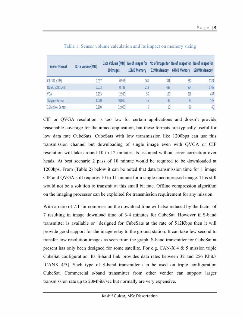
Table 1: Sensor volume calculation and its impact on memory sizing
CIF or QVGA resolution is too low for certain applications and doesn’t provide
reasonable coverage for the aimed application, but these formats are typically useful for
low data rate CubeSats. CubeSats with low transmission like 1200bps can use this
transmission channel but downloading of single image even with QVGA or CIF
resolution will take around 10 to 12 minutes its assumed without error correction over
heads. At best scenario 2 pass of 10 minute would be required to be downloaded at
1200bps. From (Table 2) below it can be noted that data transmission time for 1 image
CIF and QVGA still requires 10 to 11 minute for a single uncompressed image. This still
would not be a solution to transmit at this small bit rate. Offline compression algorithm
on the imaging processor can be exploited for transmission requirement for any mission.
With a ratio of 7:1 for compression the download time will also reduced by the factor of
7 resulting in image download time of 3-4 minutes for CubeSat. However if S-band
transmitter is available or designed for CubeSats at the rate of 512Kbps then it will
provide good support for the image relay to the ground station. It can take few second to
transfer low resolution images as seen from the graph. S-band transmitter for CubeSat at
present has only been designed for some satellite. For e.g. CAN-X 4 & 5 mission triple
CubeSat configuration. Its S-band link provides data rates between 32 and 256 Kbit/s
[CANX 4/5]. Such type of S-band transmitter can be used on triple configuration
CubeSat. Commercial s-band transmitter from other vendor can support larger
transmission rate up to 20Mbits/sec but normally are very expensive.
Sensor Format Data Volume[MB]Data Volume [MB]
10 images
No of Images for
16MB Memory
No of Images for
32MB Memory
No of Images for
64MB Memory
No of Images for
128MB Memory
CIF(352 x 288) 0.097 0.967 165 331 662 1324
QVGA( 320 × 240) 0.073 0.732 218 437 874 1748
VGA 0.293 2.930 55 109 218 437
1M pixel Sensor 1.000 10.000 16 32 64 128
3.2M pixel Sensor 3.200 32.000 5 10 20 40

2
O
P
th
re
fo
th
ac
h
S
su
W
m
d
M
C
Q
V
1
3
Table
2.4 Requ
Optics size h
reliminary c
he applicatio
eport a prelim
or such mult
he scope of
ctivity. Here
as been dis
ome of the
uch optics de
With frequen
multiple app
esigns can b
Most applica
CIF(352 x 288)
QVGA( 320 × 24
VGA
1M pixel Senso
3.2M pixel Sen
Sensor Form
2: Transmis
uirement
has more stri
camera desig
on needs dep
minary asse
ti application
f this thesis
e in this the
scussed wit
se applicatio
esigns are po
nt developme
plication su
be improved
ations also h
for 1200
40)
or
sor
Tra
at
Kashif G
ssion time to
t analysi
ingent requi
gn in this sec
pending on o
ssment on o
n system req
and carried
esis the optic
th several a
ons have ha
ossible to de
ent and testi
upport can
d for particu
have very p
0bps fo
676
512
2048
6991
22370
ansmission Ti
w
Gulzar, MSc D
o send single
s for app
rements and
ction has be
optics, proce
optics param
quires the de
d out as a s
cal requirem
applications
arsh require
evelop and te
ing on smal
be mature
ular applica
precise cont
r 115200bps
ime to Send S
without error
Dissertation
image for d
plication
d differs from
en discussed
essing and m
meter have be
etail analysis
supporting
ments scale
in mind.
ements but
est.
ll satellites
ed. Optics
ation need.
trol and
for 9600
7
5
21
73
233
Single Image
Correction o
different sens
n
m applicatio
d with respe
memory requ
een performe
s and design
bps fo
84
64
256
874
2796
to Ground St
over Head
Figure 3: F
P a g e
sor format
on to applica
ect to the som
uirements. In
ed. Optics d
which is be
or 512Kbps
tation[sec]
ocal length c
e | 10
ation.
me of
n this
design
eyond
2
1
5
16
51
concept

P a g e | 11
Kashif Gulzar, MSc Dissertation
pointing, agility and stability requirements.
With regard to optics design following conventional optics design diagram shown in
(Figure 3) have been considered. From the figure focal length and pixel detector size are
related by following relation.
(2.b)
· (2.c)
Where
P = Pixel size or detector Size.
TSD = Sampling distance of the target it specifies the size of the target object that
can be accommodated into the system. With respect to Earth observation
this simply specify the Ground Sampling Distance or GSD
H = Distance of the object from the sensor with regard to Earth observation it’s
the height of the satellite
f = Focal length of the system.
In optics, the f-number (sometimes called focal ratio, f-ratio, or relative aperture) of an
optical system expresses the diameter of the entrance pupil in terms of the focal length of
the lens. In simpler terms, the f-number is the focal length divided by the "effective"
aperture diameter [WIKI-FSTOP].

P a g e | 12
Kashif Gulzar, MSc Dissertation
/#
(2.d)
Where
f = focal length of the system
D = diameter of the lens
2.4.1 Pixel size
For the different scenarios related to different applications assessment has been
performed for 6µm x 6µm CMOS sensor with dimension of the imager array size equal
to 640 x 480 pixels. A sensor with smaller pixel size can be selected for some of the
application but there are certain advantages of using a larger pixel size. Pixel area affects
the dynamic range of the system. Larger pixel area allows larger charge capacity and
therefore, provides wider dynamic range. It allows the brighter objects to be clearly more
visible on a darker background. Normally, a wide dynamic range is required for star
sensors. Increasing pixel size increases the S/N ratio and the performance tradeoffs are
generally not acceptable when pixel size drops below 6µm [KODAK]. When the size of
a CMOS imaging sensor array is fixed, the only way to increase sampling density and
spatial resolution is to reduce pixel size. But reducing pixel size reduces the light
sensitivity. Hence, under these constraints, there is a tradeoff between spatial resolution
and light sensitivity. Uncorrelated image noise is visible in sensor images generated by
sensor with small pixel size [FARRELL06]. For the small sensor if the sensor technology
allow to use a smaller pixel size with high dynamic range and higher SNR. Smaller pixel
size, however, requires reduced optical focal length of optics size budgets. We can use
smaller optics for a smaller pixel format sensor.
Following applications analysis has been performed for optics and electronics design.

P a g e | 13
Kashif Gulzar, MSc Dissertation
Debris monitoring
Star Sensor for small scale satellite.
Earth observation for small satellites.
Transient lunar phenomenon (TLP) study
Detection of nearby space objects.
2.4.2 Feasibility analysis of Transient Lunar Phenomena
Transient lunar phenomena (TLP) are described as short-lived changes in the brightness
of patches on the face of the Moon. They last anywhere from a few seconds to a few
hours and can grow from less than a few to a hundred kilometers in size. Most instances
of TLP are described as increases in the overall luminosity of a spot on the Moon.
However, sometimes observers report a decrease in a region's brightness or even a change
in its color to red or violet. Reports of TLP have described them as "mists", "clouds",
"volcanoes", among other provocative terms. Even today, they are poorly understood
[TLP]. These TLP require continuous observation of Moon. TLP phenomenon if reported
by astronomers can be verified by satellite based observation or vice versa. Such
detection of change require that the Moon must be imaged continuously, For this thesis
camera has been designed keeping in view of the total duty cycle operation since it is not
possible to observe the Moon continuously using a single satellite a constellation can be
designed to support such observation, or the mission must be planned in a way to support
the maximum utilization and detection. (Figure 4) shows the approximate TLP
observation scenario for Moon observation.

P a g e | 14
Kashif Gulzar, MSc Dissertation
Figure 4: TLP observation scenario
2.4.2.1 Impact on electronics
TLP’s require constant observation of the Moon. Since it is not feasible to image the
Moon continuously and transmit all images to the ground so a limit on system is to store
and transmit only the data when these short lived changes are detected. It requires
excessive burden on some image processing on board to detect, the temporal changes in
image also require powerful digital image processing hardware and high end processor
available for image processing. It requires a huge amount of processing on board for
comparison of images continuously like a target tracking mechanism. However,
compromises can be made initially using low end processors. Since the satellite will
always be in motion therefore, it requires some form of image registration before
comparison and time elapsed change between successive images must be detected with
the camera processor.
For observing such phenomenon, the operation duty cycle of the system must be almost
100%. Which provide stressed constraint on power requirements as the system needs to
be operated continuously. However, storage and transmission requirement with this
scheme is not complex as only few amount of image are required for detection so storage
will not be a big concern for this kind of application.

P a g e | 15
Kashif Gulzar, MSc Dissertation
A project is in operation at ROBOTIC LUNAR IMAGE Monitor in Cerro Tololo
Interamerican Observatory in Chile and is coordinated by Arlin Crotts, Paul Hickson,
Cameron Hummels & Thomas Pfrommer[TLP]. They have used ground based tracking
system consisting of two camera one low-resolution and high frame-rate with
specification(10km/pixel, 5Hz) and the other high-resolution camera and low frame-rate
with specification (1.2km/pixel, 0.1Hz). This system is constantly taking images of the
Moon, and use image processing algorithm for detecting TLP more sensitively than the
human eye but this system is used for ground based observations. From this we can infer
the extent of image frequency required for processing.
2.4.2.2 Optical feasibility analysis for TLP
Optics parameter for Moon has been elaborated at from 500m/pixel to 10000km per
pixels is shown in the following graph.
Figure 5: Focal length vs. ground sampling distance for Moon
To have a complete circumference of the Moon on a 640 x 480 pixel array of 6µm pixel
size with in the field of view of sensor, we have the focal length ~398.64 mm and field of
0 1000 2000 3000 4000 5000 6000 7000 8000 9000 100000
500
1000
1500
2000
2500
3000
3500
4000
4500
Ground Sampling Distance of Moon[m]
Foc
al L
engt
h[m
m]
Focal Length vs Ground Sampling Distance for Moon TLP

P a g e | 16
Kashif Gulzar, MSc Dissertation
view (FOV) of 0.5519 degrees, designing a telescope for this focal length would be a bit
complicated and will be too heavy on structure design, also it doesn’t fit in a CubeSat
with pinhole type camera design. This type of telescope can be accommodated in triple
CubeSat configuration with proper advance design.
For F#=2 focal length vs. aperture has been show for the above calculation with respect
to the sampling distance. The same telescope if used for Earth observation will give the
GSD of 10.558 meters. These numbers are just to give the extent of the design. Same
telescope can be used for acquiring both Earth and Moon images but optics requirements
for such design are quite stringent and challenging and it is difficult to accommodate in
small configuration CubeSat structure. To reduce the optical constraints one preposition
is to use a smaller pixel size. Second proposition is to get a smaller Moon size on the
sensor image plane.
Figure 6: Focal length vs. aperture
0 500 1000 1500 2000 25000
500
1000
1500
2000
2500
3000
3500
4000
4500
Aperture[mm]
Foc
al L
engt
h[m
m]
Focal Lenght vs. Aperture

P a g e | 17
Kashif Gulzar, MSc Dissertation
2.4.2.3 Requirement defined for TLP
REQ_TLP_001. Frequency of image for algorithm application can be either 5 to 6 images
per minute. Requirement is inferred from the Ref [TLP]. However this requirement is
difficult to be met without DMA based DSP processor.
REQ_TLP_002. Storage for at least storage of 10 images on reasonable change detection.
REQ_TLP_003. System will not register more than specified amount of images after a
change is detected or system and frequency of image take can be made reconfigurable or
adaptive. (Based on the detection logic and Phenomenon detection scheme)
REQ_TLP_004. Continuous operation must be ensured during the duration of mission in
order not to miss such phenomenon depending on the view of Moon insight in orbit.
REQ_TLP_005. Combination of satellites must be used to monitor different areas of
Moon. Orbits must be defined depending on particular mission requirements.
REQ_TLP_006. Continuous availability and processing of Images for change detection.
REQ_TLP_007. In time processing and storage is required. Image can be transmitted
whenever system will be in contact with ground station.
2.4.3 Earth observation
Small satellite camera on a Pico and Nano satellite provides a valuable resource for Earth
observation.
Figure 7: Camera use as Earth observation scenario

P a g e | 18
Kashif Gulzar, MSc Dissertation
Depending on the mission scenario it could be used as a main application of the camera
or the secondary application. Mostly, with other application it can be satisfactorily use as
secondary application. For Earth observation we have the same problem with regard to
telescope design. Following calculation shows the effect of GSD on optical focal length.
The f/# is kept to be f/2 to provide the appropriate focal length to diameter ratio. This
ratio can be used for smaller focal length but for larger focal length, greater f/# must be
chosen to allow for appropriate telescope size. Following calculation has been performed
to show some of the impact on system sizing due to larger focal length.
Figure 8: Focal length vs. Ground Sampling Distance for Earth observation
To have a complete disk of Earth in view of camera of a 640x480 array image plane with
6µm pixel we require FOV of 167.47 degree which is not feasible as wide field of view
make the image inappropriate. A lower FOV must be selected for Earth observation. For
particular mission, the reasonable coverage on Earth must be defined and particular
optics must be selected with support to the other application on-board, With regard to
multiple on-board application of the same device Earth observation can be made
secondary application for the cube sat missions.
100
101
102
103
104
105
0
100
200
300
400
500
600
700
800
900
Ground Sampling Distance(GSD) for Earth observation[m]
Foc
al L
engt
h[m
m]
Focal Length vs Ground Sampling Distance(GSD) for Earth Observation

P a g e | 19
Kashif Gulzar, MSc Dissertation
Figure 9: Focal length vs. aperture for Earth observation
2.4.3.1 Requirements with regard to Earth observation
If camera has to support the multiple observations then the Earth observation parameter
can be greatly influence by the added application to the system making the requirement
for the Earth observation a secondary objective. Means that first the system is
parameterized for primary application and then the Earth observation parameter must be
evaluated get the idea of resolution inferred for supporting Earth observation.
2.4.4 Star sensor
Star sensor is used for attitude determination. They provide accurate attitude
determination vectors for satellite. For Star Sensor, the field of view and sensitivity of the
sensor play an important role for the design. Following requirements are inferred.
REQ_STR_001. It must have the capability to store star catalog in flash almost 200KB
minimum is required for the parallel for star sensor algorithm carried out in university of
Würzburg. A larger support for star catalog can be made possible as this requirement
doesn’t conflict with the storage requirement for the system.
0 50 100 150 200 250 300 350 400 4500
100
200
300
400
500
600
700
800
900
Aperture[mm]
Foc
al L
engt
h[m
m]
Focal Lenght vs Aperture for F#=2

P a g e | 20
Kashif Gulzar, MSc Dissertation
REQ_STR_002. DSP support will be an advantage for running computation intensive
algorithm.
REQ_STR_003. The dynamic range of the Star Sensor must be limited to stars with a
visual magnitude range MV 2.5 to 6.5 [STEYN]
REQ_STR_004. Star Sensor must have memory to store at least 5 images or greater per
second for image processing.
REQ_STR_005. FOV should be in the range of 7 degrees to 30 degrees. [STEYN]
provide a good ref for selection of reasonable FOV for Sensor. .
SWATH tanFOV deg · π2 · 180
· 2 · H figure 3
(2.e)
Field of view 10 degrees
F# of 1.4
Pixel detector Size = 6µm x 6µm
Using Equation (2.d) For a 10 degree field of view we would require a focal length of
22mm which is affordable for CubeSat based satellite if the mass budget of the complete
satellite permits to allow use of such optics. Moreover, for Star Sensor it is generally
required reasonable size baffle to protect it from stray light. For the secondary application
of earth observation with start sensor system we can get the swath width of 128.48 km
with a ground sampling distance of 191 meters for Earth observation.
2.4.5 Space debris monitoring
Space debris monitoring is another important and challenging candidate for camera on-
board for small satellite. After the launch of first satellite sputnik, many satellites have
been launched into the various orbit of Earth. Most of these satellite and launched
material kept on circulation around the Earth without any control. Many systems,

P a g e | 21
Kashif Gulzar, MSc Dissertation
previously launched in space, have been discarded due to non functionality orbital debris
generally refers to material that is on orbit as the result of space missions, but is no longer
serving any function. The launch vehicles or anything which are left in space contribute
to the space debris. They have typically involved the release of items such as separation
bolts, lens caps, momentum flywheels, nuclear reactor cores, clamp bands, auxiliary
motors, launch vehicle fairings, and adapter shrouds. Approximately 70,000 objects
estimated to be 2 cm in size have been observed in the 850-1,000 km altitude band. At
altitudes of 2,000 km and lower, it is generally accepted that the debris population
dominates the natural meteoroid population for object sizes 1 mm and larger [AERO].
Following graph shows the increasing trend in space object.
Figure 10: Earth objects in orbit [NASA-OD]

P a g e | 22
Kashif Gulzar, MSc Dissertation
Space debris must be sunlit and the background must be dark in order for the optics to
detect particular kind of debris [UN99]. Optics design does imply to specify the
minimum size to detect debris. 1cm to 10 cm debris size has been used for the assessment
of optics design with respect to the distance of debris from optics or satellite detecting
debris. Distance up to 6km from the satellite orbit has been used for calculating optical
parameter like focal length with respect to space debris distance
Following graph shows the orbital debris focal length for the size of 6µm x 6µm pixel
camera and f/2 f-stop value. The graph compared the distance of object from the satellite
up to 6km using the orbital debris size from 1 to 10cm, acquired by single pixel for a 640
x 480 resolution image plane.
Figure 11: Focal length vs. space debris size

P a g e | 23
Kashif Gulzar, MSc Dissertation
2.4.6 Overall requirements
REQ_PRJ_001. The system must support the capability to adapt to particular application
need.
REQ_PRJ_002. Reasonable on board memory should be provided to support more than
one application.
REQ_PRJ_003. Since the various application have different optical need therefore, if the
optical design permit then suitable focal length must be chosen to support multiple
application.
REQ_PRJ_004. The camera should have the ability to support 100% duty cycle.
REQ_PRJ_005. Camera must support power down mode.
REQ_PRJ_006. It must provide interface to support S-Band transmitter data rates.
REQ_PRJ_007. It must be able to receive onboard command using RS232 or CAN base
interface.
REQ_PRJ_008. It must provide acquisition space for minimum of 10 images.
REQ_PRJ_009. It must be as small as possible and weight and power should be saved to
the minimum.
2.4.7 Telescope size
Telescope with larger focal length can be designed compactly. Ideally the telescope sizes
are dictated by focal length. With a single lens design system the length of telescope
would be the same as the focal length however, with multiple bending of light telescope
size can be reduced. Size can be considerably reduced by using the reflective telescope.
Designing or purchasing telescope for size reduction is very costly. Some of work related
to telescope design has been demonstrated by Nano-JASMINE satellite. It has a Ritchey-
Chretien type telescope with a 5-cm effective aperture, a 167-cm focal length and a field

P a g e | 24
Kashif Gulzar, MSc Dissertation
of view of 0.5x0.5 degree. The telescope only occupies a volume about 15x12x12 cm,
and weighs two kilograms or less [JASMINE]. This implies the reduction in telescope
length to the factor of 11.13 as compared to focal length.

P a g e | 25
Kashif Gulzar, MSc Dissertation
Chapter 3
Previous Work
3.1 Existing satellites with camera
Following explanation summarizes some of the existing CubeSats with camera. The
discussion is with respect to only Picosatellite especially the CubeSats as they specify the
minimum requirements.
3.1.1 CubeSat XI-IV
CubeSat XI-IV was a Pico satellite built by Nakasuka laboratory and is launched in 2003
by Russian rocket “Rockot”, it purpose was to verify commercial off- the shelf
component it has on board camera (Figure 12) below shows the images of earth taken by
CubeSat [PRISM XI-IV].
Figure 12: CubeSat images taken University of Tokyo by CubeSat [PRISM XI-IV]

P a g e | 26
Kashif Gulzar, MSc Dissertation
3.1.2 COMPASS-1
COMPASS-1 was a CubeSat developed Aachen University of Applied Science, Germany
and launched on April 28th 2008 [COMPASS-1]. Its purpose is to let take pictures of the
Earth from the unique point of view of a satellite in orbit. It incorporated CMOS Sensor
OV7648FB camera module.
3.1.3 AAU-CubeSat
This satellite launched in 2003 was developed by Danish students of Aalborg University
was launched in 2003. The imaging payload of this satellite consists of a camera which
was developed using the Motorola CMOS sensor MCM20027. This sensor has a
resolution of 1280 x 768. This satellite has used DMA interface [AAU].
3.1.4 CanX-1
CanX-1 is developed by students of the University of Toronto. The objective of CanX-1
is to verify the functionality of several technologies in orbital space. Color and
monochrome CMOS imagers for testing for imaging star fields, the moon, and the Earth.
The objective was to verify the ability to perform star/moon/horizon tracking as part of a
complete attitude determination system [CanX-1].
CanX-1 carries two independent high-resolution CMOS imagers, together with associated
optics and electronics. The purpose of these imagers is to
Validate the use of spaceborne CMOS imagers for science and engineering.
Provide starfield images for the purpose of attitude determination via star- and
Moon tracking, as well as Earth-horizon tracking.
Provide educational images of the Moon and the Earth.
Following two Imagers were used on the system and compression is implemented in
software.

P a g e | 27
Kashif Gulzar, MSc Dissertation
Table 3: Imager specifications CanX-1[CanX-1]
Color Monochrome
Model HDCS-2020 ADCS-2120 Quantum Eff. 33% 38% Fill Factor 42% 42% Lens Focal Length 2.1 mm 25 mm Lens Aperture f/2 f/2.5 Diag. FOV 112º 14º Res. @ Nadir 1.5 km/pixel 200 m/pixel Power 200 mW 200 mW
3.2 Existing hardware solutions
3.2.1 C628 enhanced JPEG module
This is a small, lightweight and low power consumption device including most of the
features of a Digital Still Camera (DSC) such as snapshot, video capture, date-time
stamp, file management and others. By using external micro-controller, together with a
well-developed, user-friendly command, people can build a custom made camera for
specific application. Although this can be used for Nanosatellite based application or
triple configuration CubeSat but for Picosatellite range it’s not suitable because of size
and mass budgets. Camera is based on Zoran imaging processor. There are two version of
this processor Zoran coach-6E and 6P imaging processor. This processor can be used for
camera design and is one of the good solution with regard to system design, however,
since in-house camera should be developed to support maximum re-configurability,
therefore, use of BGA packages have been avoided but for camera integrator on satellite
system this processor is one of the best off the shelf solution.
Table 4: C628 enhanced JPEG module specifications [C628]
Image Sensor MegaPixels CMOS sensor Image Processor ZORAN COACH-6E On Board Memory 64Mb Storage Resident 16MB NAND Flash

P a g e | 28
Kashif Gulzar, MSc Dissertation
Video Capture 640 × 480 (30 fps) 320 × 240 (30 fps) Unlimited Motion JPEG capturing time depends on available memory space
Photo Resolution
1280 × 960, 640x480 JPEG format
White Balance Normal / Daylight / Tungsten / Floures / Cloudy
UART Baud Rate 115200, 57600 TV out NTSC / PAL USB Interface USB 1.1
Mass storage mode Supported OS: Win2000 / XP / ME
Power DC 5V
Figure 13: Functional diagram C628 module
Compression engine is separate from the acquisition path as shown in (Figure 13) and
therefore, this sensor system seems to more probable candidate in term of available
hardware in the market.

P a g e | 29
Kashif Gulzar, MSc Dissertation
3.2.2 C328R Jpeg compression VGA camera module [C328R]
C328R is neat camera which can be purchased with different lenses. These cameras are
controlled by commands send over serial interface, so there are just four cables (Tx, Rx,
+3.3V, Gnd). Communication logic is TTL so additional circuit is required when
connecting to RS-232 port. The best feature on this camera is ability to produce
directly Jpeg images or 'raw' format images in different color depth and sizes. Camera
resolution is VGA so pictures from 80 x 60 to 640 x 480 can be taken.
3.2.2.1 Features
Small in size, 20mm x 28mm
VGA resolution, down sample to QVGA or CIF
3.3V operation
Low power consumption 60mA
User friendly commands to control the module
UART interface of up to 115.2Kbps
Auto detect baud rate and make connection to the host
Power saving mode
Various lens options
Figure 14: C328R Jpeg compression VGA camera module [C328R]

P a g e | 30
Kashif Gulzar, MSc Dissertation
This camera would be appropriate for some application like taking images of Earth and
Moon in CubeSat it requires very less power and provide compression support and can be
added to any CubeSat where time critical imaging and faster processing of images is not
required. Following block diagram will give an overview of this camera.
Figure 15: Block diagram C328R camera module [C328R]
3.2.3 C3188A sensor module
The C3188A is a 1/3" color camera module with digital output that uses the
OmniVision OV7620 highly integrated CMOS digital color video camera chip. Digital
video port supplies a continuous 8/16 bit-wide image data stream. All camera functions,
such as exposure, gamma, gain, white balance, color matrix, windowing, are
programmable through I2C interface [C3188A]. This camera module was used on
university of Tokyo CubeSat XI-IV.
Figure 16: C3188A camera module [C3188A]

P a g e | 31
Kashif Gulzar, MSc Dissertation
Table 5: C3188A camera module specifications [C3188A]
Imager OV7620, CMOS image sensor Array Size 664 x 492 pixels Pixel size 7.6µm x 7.6 µm Scanning Progressive / interlace Effective image area 4.86mm x 3.64mm Electronic Exposure 500:1 Gamma Correction 128 curve settings S/N Ratio >48dB
Min Illumination 2.5lux @F1.4 Operation Voltage 5 VDC Operation Current 120mW Active 10 µW Standby Lens f6mm, F1.6
3.2.4 OV7648FB camera module
This camera module has OV7648 Camera Chip image sensor with flexible cable
employed in Aachen University of Applied Sciences CubeSat Compass-1 launch on
28.April.2008.
Figure 17: OV7648FB camera module [OV7648FB]
3.2.4.1 Features
Following table outline the features of OV7648FB Camera Module.

P a g e | 32
Kashif Gulzar, MSc Dissertation
Table 6: Key specifications OV7648FB camera module [OV7648FB]
Array Size VGA 640 x 480 QVGA 320 x 240
Power Supply Core 2.4V to 2.6V DC I/O 2.25V to 3.6V DC
Power Requirements Active 40 mW Standby 25 μW
Output Formats (8-bit) • YUV/YCbCr 4:2:2 ITU-656 •Raw RGB Data
Lens Size 1/4" Maximum Image Transfer Rate
VGA 30 fps QVGA 60 fps
Min. Illumination (3000K) f1.2 < 1 lux f2.8 < 5 lux
S/N Ratio 46 dB (AGC off, Gamma=1) Dynamic Range > 48 dB (due to 8-bit ADC limitation)
62 db for internal signal Scan Mode Progressive Exposure Time 523 to 1 line period (at selected frame
rate) Gamma Correction 0.45/1.0 Pixel Size 5.6 μm x 5.6 μm Dark Current 30 mV/s Fixed Pattern Noise < 0.03% of VPEAK-TO-PEAK Image Area 3.6 mm x 2.7 mm Package Dimensions 10mm x 9mm x 7.34mm
3.2.5 CMUCAM 3 camera
Another small camera is that can be used for image acquisition and tracking applications
is CMUcam3 hardware platform can be used for acquiring Images it is connected to
LPC2106 ARM7TDMI processor. It is a FIFO based camera which has following
features
CIF resolution (352x288) RGB color sensor
Open source development environment for Windows and Linux
MMC Flash Slot with FAT16 driver support
Four-port Servo Controller
Load Images into Memory at 26 Frames per Second

P a g e | 33
Kashif Gulzar, MSc Dissertation
FIFO image buffer for multiple pass hi-res image processing
Figure 18: CMUcam3 block diagram [CMUCAM3]
3.3 Existing optics procurement and design solutions
3.3.1 LENS selection
For the prototype the recommended optics supporting particular sensor format will be
used. However, for particular application needs, optics has to be designed according to
application perspective. Survey on small optics has been done and one manufacturer
Edmond optics has been found supplying micro lenses and optics for camera. Mostly for
different scenario custom optics design and development would be appreciated to satisfy
application needs.
Table 7: Small optical lenses
Focal
Lengt
h
(mm)
Max.
Sensor
Forma
t
f /
#
Angula
r
FOV*
Min.
Workin
g
Distanc
e
Distortio
n @ Full
Field
Max. Res.***
(lp/mm)
A
(mm
)
B
(mm
)
C
(mm
)
D
(mm
)
Mountin
g
Thread On
Axis
0.7
Fiel
d
Full
Fiel
d
1.68 1/4" 2.
5
132.9° 400mm -83.90% 169 80 — 15.0 13.2 3.3 2.8 M12 x
0.5

P a g e | 34
Kashif Gulzar, MSc Dissertation
1.7 1/4" 2.
8
109° 400mm -60% 124 87 30 21.0 19.6 4.0 3.2 M12 x
0.5
1.9 1/4" 2.
0
118° 400mm — — — — 17.0 14.5 4.2 4 M12 x
0.5
2.2 1/3" 2.
5
130° 400mm -48.5% 100*
*
63*
*
40*
*
17.0 18.3 4.8 3.7 M12 x
0.5
2.5 1/3" 2.
5
112° 400mm -60% 63 48 30 17.0 20.1 4.6 3.8 M12 x
0.5
2.9 1/3" 2.
0
96° 400mm -36.0% 63 63 40 15.0 18.0 5.2 6.4 M12 x
0.5
3.0 1/3" 2.
0
98.7° 400mm -52.10% 97 62 35 14.0 15.1 5.3 3.9 M12 x
0.5
3.6 1/3" 2.
0
72° 400mm — — — — 14.0 16.1 4.4 4.0 M12 x
0.5
3.9 1/3" 2.
0
74° 400mm -29% 88 54 46 14.0 16.0 5.9 4.0 M12 x
0.5
4.3 1/3" 1.
8
60° 300mm -24.2% 70 50 30 15.0 13.8 3.3 3.3 M12 x
0.5
6.0 1/3" 1.
7
44° 400mm -10% 72 55 46 15.0 15.3 8.0 6.0 M12 x
0.5
6.4 1/3" 2.
4
42.2° 400mm -2.40% 80 63 25 14.8 13.1 5.3 3.3 M12 x
0.5
8.0 1/3" 2.
5
30.9° 800mm <-3.0% 80 63 63 15.0 13.5 5.8 3.0 M12 x
0.5
10.06† 1/2" 2.
8
36° 400mm -0.57% 81 54 64 15.0 13.4 6.1 3.2 M12 x
0.5
10.4† 1/2" 2.
8
35° 400mm -2.00% 93 90 88 14.0 12.0 6.4 4 M12 x
0.5
12.0 1/3" 2.
0
22.3° 800mm -0.15% 63 60 60 14.0 12.0 6.4 4.0 M12 x
0.5
16.0 1/3" 2.
0
17° 400mm -2.50% 75 65 60 14.0 14.4 8 4.5 M12 x
0.5
25.0 1/3" 2.
5
10.7° 200mm -0.46% 83 58 58 25.0 23.5 8.0 6.7 M12 x
0.5
35.0 2/3" 2.
0
17° 200mm -1.10% 160 100 80 25.0 23.4 15.8 16.4 M12 x
0.5
50.0 1/2" 2.
5
6.8° 400mm -1.20% 160 100 80 27.0 48.8 8.0 41.8 M12 x
0.5
Maximum focal length available for this sensor is 50mm. with the largest lens dimension
of 4.8 mm which can be incorporated for the mission. However, these lenses provide

P a g e | 35
Kashif Gulzar, MSc Dissertation
standard mount type and a coupling structure need to be developed within the satellite
structure to use these lenses with standard C-mount type adaptor. A larger optics can be
use for Nanosatellite range satellites.
Figure 19: Infinite conjugate micro lenses [EDMUND]
Figure 20: C mount adapter [EDMUND]
3.3.2 Optics design solutions for small size satellite
Optics design is deeply constrained for small satellite and for CubeSat using a larger
optics is infeasible. However, state of the art technology can be developed in this regard.
Performing the survey from the web following two design solutions for optic found quite
appealing. Since the telescope is not designed for the work carried out in this thesis but
the two approaches given below can be used for the system if design budget permit to use
these state of the art technologies.

P a g e | 36
Kashif Gulzar, MSc Dissertation
3.3.2.1 Ultra thin telephoto lens
These Ultra thin lenses were developed by researchers at University of California San
Diego (UCSD). They created the ultra thin camera using origami to fold up the telephoto
lens. Imager is around seven times more powerful than a standard lens of the same depth
meaning cameras can now be much thinner and more powerful at the same time
[ALTOFT07].
Ultrathin high-quality image is based on an extension of conventional astronomical
telescopes such as the Cassegrain telescope, with additional folding shown in Figure
below. Light enters the element through an outer annular aperture and is focused by a
series of concentric zone reflectors to the image plane in the central area of the optics.
Figure 21 shows this concept [TREMBLAY07].
.
Figure 21: (a) Conventional lens. (b) Annular folded optics concept [TREMBLAY07]
3.3.2.2 Deployable optics
One of other techniques to reduce the length of the telescope or to be incorporated within
the structure of the Nanosatellite is to use deployable optical concept. This concept was
successfully used in PRISM, which is a remote sensing Nanosatellite. Similar kind of
deployable telescope design can be used on CubeSat Structure. Following image of
PRISM satellite from [PRISM] shows this deployable telescope concept.

P a g e | 37
Kashif Gulzar, MSc Dissertation
Figure 22: PRISM satellite deployable optics [PRISM]

P a g e | 38
Kashif Gulzar, MSc Dissertation
Chapter 4
Architecture design
4.1 System architecture
There are invariably many designs option on which camera architecture can be based.
One approach is to use shared memory and transfer this data to memory and read this
data by processor, after the images have been stored in the memory following diagram
accessed from [BEYONDLOGIC] summarize this approach. This approach is useful and
can be used in the system however, this approach requires to CPLD or FPGA in the
acquisition chain.
Figure 23: Camera architecture-1 [BEYONDLOGIC]

P a g e | 39
Kashif Gulzar, MSc Dissertation
Second approach is to use a FIFO based design as given for [CMUCAM3]. There are
many DSP processors in the market which has these Asynchronous FIFO built into the
chip and can be used for the system. However, due to the ease of using ARM processor,
and to avoid costly solution, DSP approach is avoided for this design. TI and Analog
devices DSP offer the performance solution in term of processing power and can be used
for Nanosatellite. DSP based imaging processors are expensive in term overall
development cost and require more development time than conventional processor.
One more important design aspect is to use FPGA, and built the whole design in single
chip, a single chip design approach is the best approach. However, due to the same
reasons as outlined for DSP above this design approach has been avoided. For
architecture following is proposed based on the above discussion. The selected
architecture reasonably provide the good margin for faster image acquisition and suitable
for many applications.
This camera prototype is designed to support Picosatellite and Nanosatellite applications.
Function of the imaging system is to support the different application, provide storage
capability for the system and provide interface for the OBC and transceiver. Mostly for
Nanosatellite launch cost is much greater then Picosatellite or CubeSat standard so
reliability is the most important factor for such class of satellite. Failure of payload or any
component on such class of satellite is unavoidable. However, CubeSat standard satellites
normally rely on non-space rated Commercial-Off-The-Shelf (COTS) components.
Reliability is an issue but small size doesn’t permit the use of redundant hardware mostly
due to power requirements which is indirectly related to mass budget. Triple
configuration CubeSat provides the use of a bit larger components if desired.

P a g e | 40
Kashif Gulzar, MSc Dissertation
Figure 24: Proposed system architecture-2
Application like Star Sensor and Debris monitoring and TLP are mostly driving the
system design for the processing part and other application like Remote Earth
Observation and others require long time memory storage. For this camera, design is

P a g e | 41
Kashif Gulzar, MSc Dissertation
based my on architecture similar to one of the Star Sensor design proposed in the paper
[STEYN] and [CMUCAM3] but with innovative DMA based solution. This design has
more flexibility many component can be re configured for particular application needs
also it provide more flexibility for larger design. Mostly, cameras for commercial use and
mobile phones also follow similar kind of design approaches, and are based on high end
DSP and imaging processors.
Many cameras which require a single shot can only manage one intermediate buffer
memory as a FIFO similar to equal to the size of image to store. A single image buffering
allows transfer of this image to the ground station at later stages. Camera design approach
is kept as modular, meaning that the sensor and FIFO will be designed on single PCB and
processing board with storage element will be constructed on other board. For CubeSats
if it’s only desired to take snapshots then the camera sensor board with FIFO can be
directly interfaced to OBC I/O’s. This offer saving in term of power budgets and
formulate it use feasible on satellite like CubeSat. The architecture is normally easy to
implement and can be used for application like snapshot of Earth. CubeSats transmission
rate are normally not feasible to download in a single pass or without compression.
Compression unit as a separate solution is not proposed, however, offline processing can
be done onboard to transfer images to ground station. This discussed approach is feasible
when simultaneous multiple images are not required in performing any calculation on
board on images. Following section discuss the components selection criteria for the
system on which the component have been selected and henceforth, provides the detail
feature and discussion for selected component.
4.2 Sensor
4.2.1 CCD Vs CMOS
System Dynamic Range: Dynamic Range (DR) is the ratio of the maximum output signal,
or saturation level, of an image sensor to the dark noise level or minimum level of the

P a g e | 42
Kashif Gulzar, MSc Dissertation
imager [KODAK SENSOR]. CCD sensors are better in term of dynamic range
[LITWILLER].
DR 20. logVV
(4.a)
Responsivity: The imager output voltage per incident optical energy density is called the
imager responsivity, and it is expressed in volts per micro-joule per centimeter squared,
or V/ (J/cm2) [KODAK SENSOR]. Both technologies are more or less similar in term of
responsivity. CMOS imagers are marginally superior to CCD as gain elements can be
placed and integrated on the chip [LITWILLER].
Reliability: Both technologies are more or less comparable in term of reliability.
Power: CMOS sensors consume less power than similar CCD sensors. Also for CMOS
sensor a single supply at the chip interface provide additive advantage over CCD.
Size: CMOS has the advantage to provide higher system integration. Many components
are integrated on the sensor chip. This means there are some DSP processing block and
A/D converters as well as programming interface for windowing operation available in
chip.
Speed: CMOS arguably has the advantage over CCDs because all camera functions can
be placed on the image sensor. With one die, signal and power trace distances can be
shorter, with less inductance, capacitance and propagation delays. To date, though,
CMOS imagers have established only modest advantages in this regard, largely because
of early focus on consumer applications that do not demand notably high speeds
compared with the CCD’s industrial, scientific and medical applications [LITWILLER].
Blooming: Overflow of photo-generated charge is termed blooming. The result of
blooming is a corrupted image near the blooming site. The extent of the image
degradation is dependent on the level of excess charge and on the architecture of the

P a g e | 43
Kashif Gulzar, MSc Dissertation
imager being used [KODAK SENSOR]. CMOS has natural antiblooming immunity to
counter blooming. CCD require some specific engineering to achieve such structure,
however this can be built-in on chip, but consumer grade CCD have mostly lacks anti-
blooming structures [LITWILLER].
Windowing: One unique capability of CMOS sensor is the windowing. The portion or
window of image can be read which provide additional advantage of reduced size images
or preview before being download or region of interest kind of operation. CCD sensor
has minimal support for windowing [LITWILLER].
Biasing and clocking: CCD requires some extra hardware for clock generation and some
external clock drivers for impedance matching. This requires clock generation hardware
for several CCD phase clock in term of PLDs or CPLDs. With CMOS no such clocking
hardware is required and mostly the clocking and synchronizing components are built in
to the system, therefore, CMOS provide a better solution in term of complexity of system
design [LITWILLER].
With the above discussion use of CCD sensor has been ruled out, and it has been decided
to use CMOS sensor for application. Star Sensors have already been built for space using
CMOS sensor which is one of the applications proposed for the project. In any case
system in which absolute calibration is must and uniformity of sensor pixels plays
important role care must be taken and calibration and correction techniques should be
performed. For the Star Sensor dynamic range and S/N ratio is of most important
concern.
4.3 Available CMOS sensors survey and selection
Market survey of available sensor has been performed. There are many sensors available
in market. A complete and thorough survey of uncountable sensor is infeasible. Sensors
used in some of the CubeSats mission provide some direction toward the selection. One
of the problems in finding some of the sensor is that no complete data sheets (only

P a g e | 44
Kashif Gulzar, MSc Dissertation
preliminary information) are available for evaluation purposes also there are other legal
issue involved. These all factor greatly influence the project completion time. Following
table outline some of the sensors in term of availability. Most appropriated moderate
candidate has been selected from the table keeping in view of also the availability, power,
and pixel size and windowing operation and availability. Since a larger pixel size was
desirable OV7720 6µm x 6µm for the sensor to be useful for Star Sensor or debris
monitoring application was selected from the table below. However, big pixel size sensor
consumes a little more power. It adds up to 40 mW to 50 mW to the whole system. This
increased figure is practically feasible.
Table 8: Selected sensor comparison
Sensor Provide
r
Resol
ution
Lower
Resolut
ion
support
Powe
r
[mW
]
Built
-in
ADC
ADC
Width
Output
Format
Temp
[ºC]
Dynamic
Range
[dB]
Pi
x
Si
ze
Packag
e
LUPA-1300 Cypres
s
1280 x
1024
Yes 900 No N
A
Analog 0 to 60 --- 14 μm
x 14
μm
--
CYIWOSC
1300AA
Cypres
s
1297H x
1041V)
Yes TBA Ye
s
10 Bayer-
pattern
0 to
+60°C
TB
A
2.8um
x
2.8um
--
MCM20027 Motoro
la
1280 x
1024
Yes 250 Ye
s
10 Bayer-
pattern
0-40 50
dB
6µm x
6µm
--
OV9655-
V28A
OmniV
ision
1280 x
1024
SXGA
Yes 90 Raw
RGB,
RGB
(GRB
RGB56),(
YUV
YCbCr)
0°C to
50°C
-- 3.18
μm x
3.18u
m
CSP
-28
OV7610(No
t Produced)
OmniV
ision
640 x 480 Yes 200 Ye
s
8/
16
bit
Raw RGB
Data,
RGB,
YUV
wi
de
8.4μm
x
8.4μm

P a g e | 45
Kashif Gulzar, MSc Dissertation
OV9665-
V26A
OmniV
ision
1280 x
1024
SXGA
Yes 80 Ye
s
10 Raw RGB
Data,
RGB,
YUV
-30 to +70 wi
de
2μm
x2μm
26-
pin
CSP
2
OV7720-
V28A
OmniV
ision
and below,
CIF,
QVGA,
VGA
Yes 120 Ye
s
10 Raw RGB
Data,
RGB,
YUV
–20 to +70 60
dB
6.0µm
x
6.0µm
CSP
-28
OV7710-
C48A
OmniV
ision
and below,
CIF,
QVGA,
VGA
Yes 140 Ye
s
10 Raw RGB
Data,
RGB,
YUV
-40 to
+105
wi
de
6.0µm
x
6.0µm
CL
CC-
48
OV7725-
V28A
OmniV
ision
and below,
CIF,
QVGA,
VGA
Yes 120 Ye
s
10 Raw RGB
Data,
RGB,
YUV
–20 to +70 60
dB
6.0µm
x
6.0µm
CSP
-28
OV7211-
F48V ™
OmniV
ision
VGA -- 140 Ye
s
10 RGB,
YUV
–20 to +70 wi
de
6.0µm
x
6.0µm
28-
pin
CSP
OV07710-
C00A
OmniV
ision
VGA -- 140m
W
Ye
s
10 10bit raw
8bit RGB,
YUV
-40 to
+105.
53
dB
6.0µm
x
6.0µm
CL
CC-
48
4.4 Sensor features
OV7720 from OmniVision sensor selected as a final candidate from (Table 8) because of
following additional features.
1. 6µm x 6µm pixel size.
2. 8 bit raw data format is available.
3. CLCC package was available which is easy for prototyping at low cost.
4. Provide SCCB interface to program and control many of the important sensor
features.
5. Automatic image control functions including:
Automatic Exposure Control (AEC)

P a g e | 46
Kashif Gulzar, MSc Dissertation
Automatic Gain Control (AGC)
Automatic White Balance (AWB)
Automatic Band Filter (ABF)
Automatic Black-Level Calibration (ABLC) This sensor is also chosen as
minimum amount of support component are needed.
6. It provides the full functionality of a single chip camera. A/D converters are built
into the chip and sensor provides the digital interface for easy integration in to
digital systems.
7. Availability and purchase issues.
8. Provide configuration supports for image sizes. VGA, QVGA, and any other size
scaling down from CIF to 40 x 30.
9. High sensitivity for low-light operation
10. Provide reasonably good dynamic range and SNR
Figure 25: Sensor OV7720

P a g e | 47
Kashif Gulzar, MSc Dissertation
4.4.1 Block diagram of the sensor OV7720
Figure 26: Internal block diagram sensor
Here sensor provides the 10 bit output on digital interface. Sensor is a ten bit sensor but
only upper 8 bits are used for the design. Data from the image array unit is sampled by
A/D converter and is passed through processing stages and finally available at output
D[9:0]. SCCB block here provide the programming interface to control the sensor
parameters. Video timing generator block provide the timing and synchronization signal
for the acquisition unit and is very useful for software synchronization through interrupts.
4.4.2 Sensor parameters
Following are the important parameters for this sensor.

P a g e | 48
Kashif Gulzar, MSc Dissertation
Table 9: OV7720 sensor parameters [OV7720]
Array Size 640 x 480
Power(Active) 120 mW typical maximum( Depends on the
image acquisition rate)
Output Format support for:
– Raw RGB(10/8 bit)
– RGB (GRB 4:2:2, RGB565/555/
444)
– YCbCr (4:2:2) formats
Maximum Image Transfer Rate 60 fps
Sensitivity 3V/(lux.sec)
SNR 50 dB
Dynamic Range 60 dB
Pixel Size 6µm x 6µm
Scan Mode Progressive
Dark Current 40mV/s
Image area 3984µm x 2592µm
Package dimension 1.143 cm X 1.143 cm
automatic image control functions
including:
– Automatic Exposure Control (AEC)
– Automatic Gain Control (AGC)
– Automatic White Balance (AWB)
– Automatic Band Filter (ABF)
– Automatic Black-Level
Calibration (ABLC)
image quality controls including
Image Window Sizes supports image sizes: VGA, QVGA,
and any size scaling down from CIF
to 40 x 30
Operating Temperature Range -20°C to +70°C
Digital Signal Processor Block Color saturation, hue, gamma,

P a g e | 49
Kashif Gulzar, MSc Dissertation
sharpness (edge enhancement),
and anti blooming
Elimination of Color Cross talk
Dynamic Range Consult [OV7720]
SNR Consult [OV7720]
4.4.3 Camera SCCB interface for configuration
4.4.4 Prototype optics for sensor
With respect to current testing in the system a compatible lens with following
specification with following parameter was used. Refer to Annex-4 for detail mechanical
specifications.
Part# 741R
Effective Focal Length (EFL) = 5.3 mm
F#= 1.9 mm Infinity
Angle of View = 55.6 deg Diagonal
45.7 deg Horizontal
35.1 deg Vertical
4.5 Processor market survey
If we want improve processing speed, we must first understand what it spends its time
doing. It is a common misconception that computers spend their time computing, that is,
carrying out arithmetic operations on user data. In practice they spend very little time
'computing' in this sense. Although they do a fair amount of arithmetic, most of this is
with addresses in order to locate the relevant data items and program routines. Then,
having found the user's data, most of the work is in moving it around rather than
processing it in any transformational sense [FURBER]

O
pr
pr
pr
in
u
A
d
ex
One of the pr
rocessing al
rocessing o
rocessors tak
nstructions. B
sed for imag
A market sur
etails of the
xternal mem
1. It mus
2. It mus
3. It mus
4. Intern
extern
Figure 27
rocessor sel
lgorithm are
of images. F
kes 43% of
Both data m
ge processing
rvey of the
e candidate
mory interfac
st have exter
st provide U
st have DMA
nal video FI
nal video FIF
Instr
Data Move
Compariso
Kashif G
7 Typical dy
ection criter
e data inten
From (Figu
the time. Se
movement ins
g algorithms
processor h
processors
ce has been s
rnal memory
UART/CAN b
A architectur
IFO can be
FO.
15%
13%
uction T
ement
on
Gulzar, MSc D
ynamic instru
ria is to use
nsive, a lot
ure 27) clea
econd time c
struction and
s.
has been per
parameters.
selected due
y interface.
based interfa
re to support
an advanta
23%
%
5% 1%
Type vs D
Control flow
Logical operat
Dissertation
uction usage
a DMA bas
of data mo
arly the dat
consuming in
d control flo
rformed. Ta
LPC2468
to following
ace for OBC
t memory in
age however
43%
Dynamic
Arth
ions Othe
e [FURBER]
sed processo
ovement is
ta movemen
nstruction is
w instructio
able in Anne
DMA based
g reasons.
C.
ntensive proc
r design pe
c Usage
hmetic operatio
er
P a g e
]
or. Mostly im
required fo
nt instructio
s the control
on are extens
ex-A provid
d processor
cesses.
rmits the u
ons
e | 50
mage
or the
on in
flow
sively
de the
with
se of

P a g e | 51
Kashif Gulzar, MSc Dissertation
5. USB interface and debugging hardware like JTAG or ISP may provide additive
advantage for application development processor.
6. On board RTC can provide time based synchronization and time tagging of image
however these function can also be controlled by OBC.
4.5.1 Selected processor features
A detail analysis of imaging processor was carried out to in term of function supported.
ARM based architecture was chosen for the application and a survey is performed on the
available ARM based processor attached in Annex-1. This table outlines the various
candidates selected for the hardware. Many of the COTS based components used in
mobile industry are very small where these IC packages are based on BGA packages
requiring excessive amount of work in term of hardware development and testing. For
these type of processor component soldering requires special equipment also inspection
for defect require X-raying techniques. One possible solution for development is to
design the system and outsource the development process but it require excessive amount
of budget.
Suitable COTS based component in term of processing have been outlined in the
following section. Power Specification of LPC2468 has not been mention specifically in
the data sheet but it can go up to maximum of 1.5 Watt based on heat dissipation values
which seems to be very large for single CubeSats, however, for multiple configured
CubeSat this power is within the power budgets. Moreover, power mentioned is based on
absolute maximum rating. Since the hardware has feature to turn off power to most of the
unused peripherals, power can be greatly reduced further buy turning off the processor
unused peripherals. Although BGA package of the device is available that can reduce the
PCB size to very minimum but for the sake of simplicity and development on the pre-
specified schedule this package use was avoided. The architecture of the processor is
shown below.

P a g e | 52
Kashif Gulzar, MSc Dissertation
Figure 28: Processor architecture [LPC2468]
The following processor features are considered for this camera design [LPC2468]
512 KB on-chip flash program memory with In-System Programming (ISP) and
In-Application Programming (IAP) capabilities. Flash program memory is on the
ARM local bus for high performance CPU access.
64 KB of SRAM on the ARM local bus for high performance CPU access.

P a g e | 53
Kashif Gulzar, MSc Dissertation
Dual Advanced High-performance Bus (AHB) system allows simultaneous
Ethernet DMA, USB DMA, and program execution from on-chip Flash with no
contention.
EMC or external memory controller provides support for asynchronous static
memory devices such as RAM, ROM and Flash, as well as dynamic memories
such as Single Data Rate SDRAM also the camera is interfaced to this EMC
block.
General Purpose AHB DMA controller (GPDMA) that can be used with the SSP,
I2S, and SD/MM interface as well as for memory-to-memory transfers.
CAN controller with two channels.
SPI controller.
Three I2C-bus interfaces (one with open-drain and two with standard port pins).
SD/MMC memory card interface.
Real-Time Clock (RTC) with separate power domain, clock source can be the
RTC oscillator or the APB clock.
Watchdog Timer (WDT). The WDT can be clocked from the internal RC
oscillator, the RTC oscillator, or the APB clock.
Boundary scans for simplified board testing.
Four reduced power modes: idle, sleep, power-down, and deep power-down.
Four external interrupt inputs configurable as edge/level sensitive. All pins on
PORT0 and PORT2 can be used as edge sensitive interrupt sources.
From the table in Annex-1, there are some of the hardware available which provide front
end video ports for direct interface to the sensor since they were only available in BGA
package therefore there use is avoided. OMAP3515 from TI has been used for developing
mobile phone based system which is best for power and other specification and can be
used as a digital signal processing hardware with support for faster algorithm execution.
If overall budget permits then this can be used efficiently for many of the task on board

P a g e | 54
Kashif Gulzar, MSc Dissertation
with support for DSP operation for CubeSat mission. But DSP based processor is a costly
solution compared to ARM processor both in term of development and project schedule.
Following discussion outline gives the description of different features of the processors
considered for this Hardware Design. These featured functions are referred from ref.
[LPC2468].
4.5.1.1 External memory controller
The LPC2468 EMC is an ARM PrimeCell MultiPort Memory Controller peripheral is
supported for asynchronous static memory devices like RAM, ROM, and Flash. In
addition, it can be used as an interface with off-chip memory-mapped devices and
peripherals. Sensor is also interfaced to this EMC bus to exploit DMA function. The
EMC is based on an Advanced Microcontroller Bus Architecture (AMBA) compliant
peripheral.
4.5.1.2 General purpose DMA controller
The GPDMA is based on AMBA AHB compliant peripheral which allow different
peripherals to have DMA support. The GPDMA allows peripheral-to-memory, memory-
to-peripheral, peripheral-to-peripheral, and memory-to-memory transactions. DMA
provides unidirectional serial DMA transfers for a single source and destination. The
source and destination areas can be accessed through the AHB master interface.
4.5.1.3 USB interface
The Universal Serial Bus (USB), a 4-wire bus which supports communication between a
host and one or more (up to 127) peripherals. The host controller allocates the USB
bandwidth to attached devices through a token-based protocol. The bus supports hot
plugging and dynamic configuration of the devices. All transactions are initiated by the
host controller. LPC2468 provides fully support compliant USB 2.0 specification (@full
speed).

P a g e | 55
Kashif Gulzar, MSc Dissertation
4.5.1.4 CAN controller
The Controller Area Network (CAN) is a serial communications protocol which
efficiently supports distributed real-time control with a very high level of security. This
communication protocol is available on many satellites and provides a very robust
interface. The CAN block is intended to carry multiple CAN buses at the same time,
allowing the device to be used as a gateway, switch, or router between two of CAN buses
in industrial or automotive and space applications.
4.5.1.5 UARTs
The LPC2468 contains four UARTs. The UARTs include a fractional baud rate
generator. Standard baud rates such as 115200 can be achieved and is used for the test
application command, control and accusation interface.
4.5.1.6 SPI Interface
The LPC2468 contains one SPI controller. SPI is a full duplex serial interface designed to
handle multiple masters and slaves connected to a given bus. Only a single master and a
single slave can communicate on the interface during a given data transfer. During data
transfer the master always sends 8 bits to 16 bits of data to the slave, and the slave always
sends 8 bits to 16 bits of data to the master
The peripheral clock that is normally used for peripherals can be derived from CPU clock
and it can run with the same max speed as ARM7 AHB at 60MHz (max). From the data
sheet it can be inferred that we can divide this with a factor of 8 or greater and SPI rate
can be calculated as 1/8 of input peripheral clock.
Maximum SPI ratPCLKSPCCR
minimum 8 (6.a)
This implies

P a g e | 56
Kashif Gulzar, MSc Dissertation
PCLK = 60MHz.
608
7.5
200 (1.a)
Since data can be transferred to S-Band transceiver around this rate therefore, is
supported by capability of S-Band Transmitter and hence can be safely used for this
purpose. It depends only on the implementation of S-Band Transceiver implementation.
4.6 FIFO for image buffering
After the processor and sensor has been selected for the proposed architecture, remaining
important hardware component is FIFO. There are two types of FIFO available one is
asynchronous FIFO which has multiple clock domains means support separate clock for
read and write operation. Second type of FIFO is synchronous FIFO which has only
single clock domain for read and write operation.
Asynchronous FIFO is only investigated due to due to the consideration for multiple
clock domains. Sensor can write the data onto the port of FIFO at its pixel clock rate and
processor can read the FIFO at its memory or port access rate. CMOS sensor can be
easily interfaced to asynchronous FIFO.
Following FIFOs were available from Averlogic and Cypress semiconductor for present
512 KB FIFO from the Averlogic AL440 was selected as it can store easily 640 x 480
size image. Sensor board with single FIFO can be used with direct interface to on board
processor.

P a g e | 57
Kashif Gulzar, MSc Dissertation
Table 10: FIFO for image acquisition selection table
Product
Descriptio
n
Configuratio
n
Application Part No. Power
Specifications
Speed Package
Full HD
FIFO
memory
8M X 16 bits Multimedia
System,
Video
Capture
System, and
various video
data buffering
AL460A 3.3
2.5V
150/75
MHz
LQFP12
8
Frame
FIFO
512K X8 bits Serial I/O
Buffer,
HDTV,
Multimedia
System
AL440B 3.3V
52 mA
171.6 mW
40/80
MHz
44-
TSOP(II)
Frame
FIFO
384K X8 bits Serial I/O
Buffer, NTSC
Video,
Multimedia
System
AL422B 3.3V
5V
45mA@30MHz,3.3
V
148.5 mW
50
MHz
28-SOP
FIFO
Cypress
512K X9bits Asynchronou
s first-in first-
out (FIFO)
buffer
CY7C421
-15AC
5V
55 mA@40 Mhz
275 mW@40 Mhz
40Mh
z
32
TPQFP
4.6.1 Al440B description
The AL440B 4Mbits (512k x 8-bit) FIFO memory provides completely independent 8bit
input and output ports it can operate at a maximum speed of 80 MHz as seen from table.
The built-in address and pointer control circuits provide a very easy-to-use memory

P a g e | 58
Kashif Gulzar, MSc Dissertation
interface that greatly reduces design time and effort [AVERLOGIC]. Following block
diagram explains the internal working of FIFO.
Figure 29: AL440B internal block diagram [AVERLOGIC]
4.6.2 FIFO features [AVERLOGIC]
4Mbits (512k x 8 bits) organization FIFO
Independent 8bit read/write port operations (different read/write data rates
acceptable)
Maximum Read/write cycle time: 80 MHz and 40 MHz (2 speed grades)
Input Enable (write mask) / Output Enable (data skipping) control
Window read/write with Mirroring capable
Selectable control signal polarity
Input Ready / Output Ready flags
Direct cascade connection
Self refresh
3.3V 10% power supply

P a g e | 59
Kashif Gulzar, MSc Dissertation
Following system design has been proposed. Selected components have been shown to
elaborate this system block diagram.
4.7 System block diagram based on selected components
In the system block diagram in (Figure 30) shown below a part from processor, sensor
and FIFO, many other options are set as optional and if particular application or group of
application demand storage and processing capability these option can be use.
Figure 30: System block diagram

P a g e | 60
Kashif Gulzar, MSc Dissertation
There is one optional interface to SDRAM left kept as a template in PCB design and
could be added for particular mission if the power budget permits. SDRAM chip requires
constant power and cannot be used as a permanent storage for long time and must be
turned on and off during the whole cycle of the missions. It should be used only for
processing temporary images. For permanent storage a flash based solution is the best
and can be used after the onboard processing has been done to store images which does
not require processing and only need to be later transmission to ground station.

P a g e | 61
Kashif Gulzar, MSc Dissertation
Chapter 5
Schematic design
Schematic for the processor board has been designed by consulting the development
board Schematic from Olimex LPC2468 development Board [LPC-E2468] and IAR Kit
development board [IAR] schematics have been attached in Annex-2 for processor board
Annex-3 for sensor board. The camera consists of two PCB modules. One module
contain sensor, FIFO buffer, and other module consists of processor with supporting
memories debug and output interfaces.
5.1 Sensor interface with FIFO
Figure show the interface between the processor and sensor.
Figure 31: Interfacing between sensor and FIFO

P a g e | 62
Kashif Gulzar, MSc Dissertation
Following signal were present at the FIFO write Interface
Table 11: FIFO write interface signals
Pin Name Pin
Number
I/O Type Description
DI[7:0] 9,8,7,6,4,3,2
,
1
I The DI pins input 8bits of data. Data input
is Synchronized with the WCK clock.
Data is acquired at the rising edge of
WCK clock.
WE 10 I WE is an input signal that controls the 8bit
input data write and write pointer
operation.
IE 11 I IE is an input signal that controls the
enabling/ Disabling of the 8bit data input
pins. The internal write address pointer is
always incremented at rising edge of
WCK by enabling WE regardless of the IE
level.
WCK 13 I WCK is the write clock input pin. The
write data input is synchronized with this
clock.
WRST 14 I The WRST is a reset input signal that
resets the write address pointer to 0.
IRDY 15 O IRDY is a status output flag that reports
the FIFO space availability.

P a g e | 63
Kashif Gulzar, MSc Dissertation
FIFO read interface contains the following signals.
Table 12: FIFO read interface signals
Pin name Pin
Number
I/O
Type
Description
DO[7:0] 36,37,38,39,
41,42,43,44
O The DO pins output 8bit of data. Data
output is synchronized with the RCK
clock. Data is output at the rising edge of
the RCK clock.
RE 35 I RE is an input signal that controls the 8bit
output data read and read pointer
operation.
OE 34 I OE is an input signal that controls the
enabling/ disabling of the 8bit data output
pins. The internal read address pointer is
always incremented at rising edge of RCK
by enabling RE regardless of the OE level.
RCK 32 I RCK is the read clock input pin. The read
data output is synchronized with this
clock.
RRST 31 I The RRST is a reset input signal that
resets the read address pointer to 0.
ORDY 30 O ORDY is a status output flag that reports
the FIFO data availability.

P a g e | 64
Kashif Gulzar, MSc Dissertation
Following signals were present in the connector for interfacing with the processor board.
The FIFO block design has been given as a reference in FIFO data sheet [AVERLOGIC]
for interfacing.
Figure 32: Connector for FIFO interfacing with processor board
Table 13: Processor board connector signals description
Pin name Pin Function I/O Signal Description
FD0…. FD7 The DO pins
output 8bit of
data.
WRST Resets the Write Address Pointer
3.3V Supply 3.3V
10%.
WE_ENA
Gnd Ground FRAME Frame Synchronization from sensor
Rrst PWDN Sensor Power Down Mode Select
IRDY ORDY
RESET_SEN automatically
Initialize
SDA_FIFO SDA carries the serial bus read/write data
bits.

P a g e | 65
Kashif Gulzar, MSc Dissertation
sensor and
FIFO chip
logic.
CS_SEN Chip select
Signal from
Processor
OE_RCK Output Rd Signal from Processor
SCL_FIFO SCL supplies
the serial bus
clock signal
to FIFO.
SDA,SDL Provide Serial Interface for Sensor
operation.
Note both serial interfaces can be made common through jumper configurations TPC1
and TPC2 shown in schematics.
5.2 Serial bus interface to FIFO
The Serial bus interface consists of the SCL (serial clock), SDA (serial data) and
/SDAEN (serial Interface enable) signals. There are pulling up circuit internally for both
SCL and SDA pins. When/SDAEN is high, the serial bus interface is disabled and both
SCL and SDA pins are pulled high. When /SDAEN is low, the serial bus interface is
enabled and data can be written into or read from theAL440B register set. For both read
and write, each byte is transferred MSB first and LSB last, and the SDA data bit is valid
when the SCL is pulled high [AVERLOGIC]. Timing relation is shown in the following
(Figure 33-34). Serial interface contain many command and will be discussed in the
software section for the project.

P a g e | 66
Kashif Gulzar, MSc Dissertation
Figure 33: AL440B Serial bus write timing
Figure 34: AL440B Serial Bus read timing
5.2.1 Interface connection of sensor board with processor.
Figure 35: Sensor board connector pin out
Signal Description Signal Description
D0…. D7 Connect to Data Bus WRST Connect to P2.4 IO

P a g e | 67
Kashif Gulzar, MSc Dissertation
3.3V Supply 3.3V to sensor
board
WE_ENA Connect to Onboard
IO Pin P2.0
Gnd Ground FRAME Frame
Synchronization from
sensor connect with
processor P2.13 and
act as an interrupt
signal
RRST P2.2 System Reset
Signal
PWDN Sensor Power Down
Mode Select connect
to P2.1
IRDY Read Reset connect to
P2.3
ORDY Reports FIFO
availability
P2.13.
RESET_SEN automatically
Initialize sensor and
FIFO chip logic.
SDA_FIFO SDA carries the serial
bus read/write data
bits.
CS_SEN Chip select Signal
from Processor
connected to CS0
OE_RCK Output Rd Signal from
Processor
SCL_FIFO SCL supplies the
serial bus clock signal
to FIFO. Connected to
processor I2C Bus
SDA,SDL Provide Serial
Interface for Sensor
operation.
. Connected to
processor I2C Bus
5.3 Sensor read operation
For the software programming and acquisition scheme the start of the VSYNC frame
generate interrupt and next start of frame generate interrupt these interrupt must be
counted between frame and sensor must be read before the next available frame is
available. We can start reading the image as soon as we get frame interrupt and empty the

P a g e | 68
Kashif Gulzar, MSc Dissertation
buffer of specified. With the DMA we can then store this data to available 16MB
SDRAM. As soon as all the images for particular application are stored in the SDRAM
processing algorithm can be started. If no processing is required the sensor can be stored
on the flash for later transmission to ground station.
The problem with utilizing storage on SDRAM is that it consumes much power and must
be turned off when there is no onboard processing however, for continuous duty cycle
application it cannot be turned off. But nevertheless storage on flash provide a better
solution in term of power saving. For CubeSat solution use of SDRAM is not
recommended. For the test application SDRAM is not used.
Figure 36: Interrupt latency for VSYNC or frame pulse
5.4 SCCB programming
Sensor has provided an SCCB interface for programming, which can directly be
interfaced to I2C. The programming protocol for two wires SCCB is quite similar to I2C.
However, there are certain difference i.e. the sensor Acknowledgement bit is don’t care
and it’s only based on three kind of transactions
3-phase write transaction cycle
2-phase write transaction cycle
2-phase read transaction cycle

P a g e | 69
Kashif Gulzar, MSc Dissertation
Phase is composed of 9 bits 8th data bits followed by 1 don’t care bit which is usually an
acknowledgement bit in I2C interface. Following figure illustrated different phases of
programming sensor registers.
Figure 37: Sensor register programming logic through SCCB using I2C[SCCB]
Phase 1: ID_Address
Phase 2: Sub_Address
Phase 3: Write Data
5.5 Memory
Up to 16MB SDRAM and 128MB Flash memory interface has been provided and
interfaced with the system this option is left configurable different memory sizes can be
used. However, if for low level mission where only picture acquisition is of important
concern and not and not the processing SDRAM use can then be avoided to save large
amount of power. Memory interface are typical design followed for the SDRAM or
FLASH and can be referred in schematics given in Appendix 2.
5.6 CAN/RS232 Interface
TJA1050 is used as the CAN transceiver. Which can provide interface for OBC operation
on can based network. Can termination resistor are provided for this system. RS232
Interface is also provided to support programming operation, testing of command and
control operation and image transmission through USB based serial cable.

P a g e | 70
Kashif Gulzar, MSc Dissertation
5.7 Debugging interface and processor clocking
12 MHz crystal is used as a main clock source. This clock source with the help of on
board PLL can be multiplied and then divided to obtain the processor operation clock.
Crystal Y2 provides the on board RTC clock. On board debugging and programming can
be performed using the JTAG interface. This connector of JTAG has been routed to P2
connector. Olimex OCD USB JTAG Debugger is used for programming and debugging.
Following figure outlines the corresponding JTAG interfacing. JTAG interface has been
provided for adding debugging capabilities to the system. This debugging interface can
be removed for flight hardware to save on board mass and space.
Figure 38: Debugging interface logic

P a g e | 71
Kashif Gulzar, MSc Dissertation
5.8 Power supply
The system is operated from 5V supply which was further regulated down to 3.3 volts for
sensor and processor and for other components on PCB. For prototype schematic system
regulation support 1.6 Watts. However, direct system voltage of 3.3V from the regulated
power bus in the satellite can support more power in that case regulator can be bypassed.
5.9 Power budgets and alternatives
Following table indicate the major component drawing system power.
Table 14: Power configuration with now optional component removed
(Typically proposed for Nanosatellite Class)
Component Power[mW]
OV7720 120
FIFO 171.6
Processor 1500 max
SDRAM
IS42S16800D
1000
FLASH
K9F2808Q0C 128MX8
OR
HY27UF081G2M 16MX8
33
UART Chip 0.99
Total 2825.59
Table 15: For CubeSat with sensor board directly interface with OBC(Alternative-1)
Component Power[mW]
OV7720 120

P a g e | 72
Kashif Gulzar, MSc Dissertation
FIFO 171.6
Total 291.6
Table 16: For CubeSat allowing the use of power up to 1 W*
Component Power[mW]
OV7720 120
FIFO 171.6
Processor (Processor can operate on power less then 500m
with many peripheral turned off)*
1500 max
FLASH
K9F2808Q0C
128MX8
HY27UF081G2M
16MX8
33
UART Chip 0.99
Total 1825.59
Above (Tables 14-16) highlight the power budget calculations. Since many of the feature
can be made configurable for particular mission. If the power budget doesn’t permit to
use full configuration of the system power can be compromised on lower functionality.
Alternatives one and two can be used depending on the power budgets for CubeSat.
Typically CubeSats have 2-10 Watts of power budgets for complete satellite.
5.10 Mass budgets
For the prototype following sensor board and processor board masses were.

P a g e | 73
Kashif Gulzar, MSc Dissertation
Table 17: Prototype mass
5.11 USB interface.
USB interface support has been provided to support high speed transfer of images to PC.
Acquisition through this interface is used and software can be developed to support
higher data rate for testing. Development of the hardware driver for the test at high speed
takes time and is beyond the scope of this thesis work.
5.12 Dimension
Sensor board = 30mm x 31mm
Processor board = 57.46mm x 57.46 mm
5.13 Modular printed circuit boards
Sensor PCB has been designed following figures shows the designed hardware for on
board camera. Design is modular and two PCBs are developed. Following figure shows
the PCB for sensor board.
Figure 39: Sensor PCB
Board Mass[grams] Sensor board with optics 11 Processor board 23

P a g e | 74
Kashif Gulzar, MSc Dissertation
Figure 40: Sensor PCB size compared to coin
Following figures shows the processor PCB and complete system designed for the
different applications.
Figure 41: Processor PCB
Complete System given with comparison for the developed camera.
Figure 42: Camera system, Euro coin and standard size card side by side

P a g e | 75
Kashif Gulzar, MSc Dissertation
Chapter 6
Software
6.1 Software for image acquisition
Embedded software in microcontroller performs various system initializations. It
initializes the processor clock, UART, I2C, Memory interfaces, IO ports functions and
DMA. It also configures sensor interrupts for frame transfer. Software state diagram
explain different microcontroller states chosen for testing purposes.
Figure 43: State flow diagram for microcontroller software

P a g e | 76
Kashif Gulzar, MSc Dissertation
Normally, after initialization microcontroller maintain it state in command acquisition by
enabling serial port interrupts, as soon as microcontroller get a valid command from the
host pc or testing application software, it respond with appropriated action. For e.g. when
microcontroller receives command for image acquisition, it acquires the image from the
FIFO and transfer it through serial port to PC and at the end of the transfer sends the valid
acknowledgment.
6.1.1 Software for sensor test application
Sensor test Application has been developed in Microsoft Visual C# 2008 Express
Edition. The software will provide the user an interface for what normally been acquired
from the image sensor. It also provides implementation for conversion algorithm.
Application has been developed to keep most of the things simple. The software sends
command through serial port and after the proper execution of the command, controller
send the acknowledgment only if the command is successful on the controller. If no
acknowledgment is received then after some time out software resumes its state.
6.1.1.1 Design considerations
Command and control and acquisition program developed to test the functionality of the
sensor and acquire Image. The user performs the different configuration of the software.
First of all select the appropriate parameter from the user interface to configure serial port
and then program the sensor through sensor initialization command via serial interface
port. These commands are received by microcontroller to program the registers specific
to the sensor. The core functionality includes the user interaction command to load the
data acquired to a text file through any terminal software for testing purpose. To acquire
image from the sensor user simply click the acquire image button after that the image will
be received by pc and displayed on the screen. The following diagram shows the main
layout of the application.

P a g e | 77
Kashif Gulzar, MSc Dissertation
Figure 44: Sensor testing program user Interface for Acquisition
Following use cases for the system was designed to fulfill different tasks. (Figure 45)
shows the case diagram developed for this system.
A. Perform Configuration
Users testing the sensor will have the flexibility to configure sensor parameter some
are specified as slider and selection values for the user. User must specify the correct
serial port for proper operation of the sensor.
A.1 Configure Image Sensor
A.1.1 Initialize defaults: Initialized the sensor with defaults for proper operation.
A.1.2 Adjust Gain (RGBA): Adjust the gain of the all channels and Individual
RGB channels
A.1.3 Flip Image (HV): for flip the image horizontally and vertically.
A.1.4 Bit & Bar Shift: Bar pattern Configuration for sensor to check the
alignment and color of sensor.

P a g e | 78
Kashif Gulzar, MSc Dissertation
A.1.5 General Register Update: Provide users the flexibility to manually input the
command and value for the required operation as stated in the data sheet.
A.2 Configure Serial Port: Use to configure serial port parameter for testing
operation 115200 baud rate must be selected by the user.
B. Load Sample File
This use case provide the user flexibility to load the sensor data saved as text file
where the sensor pixel data is save as decimal values using hyper terminal. It
provide the user additional flexibility for test purpose
C. Acquire Image
This actually sends the command to microcontroller to start sending data. The
command is use by user to trigger acquisition
D. Save Image
D.1 Save Image Bayer: This saves the image in Raw Bayer format without
RGB conversion
D.2 Save Image RGB: This will provide user to save the converted image
into RGB format and save it as bitmap file.
Figure 45: Use case diagram for sensor test application

P a g e | 79
Kashif Gulzar, MSc Dissertation
6.1.1.2 Panels to perform configuration
Following panels have been designed to support various use cases as discussed before.
Serial port configuration panel in is shown in the (Figure 46), (Figure 47) shows some of
the Control Configuration panel to configure sensor RGB gain values and also support
function to flip vertically and horizontally image in sensor hardware. (Figure 48) outlines
the advance control panel to configure sensor configuration manually it provide basic
support for sensor alignment using test pattern supported by sensor.
6.1.1.3 Software architecture
Each new control can be added by making new user control and extending it from
BaseConfiguration Class which just add a new panel in configuration tab. The class
diagram shows different classes and there relation used for the testing software.
Figure 46: Serial control
configuration panel
Figure 47: Gain control
configuration panel
Figure 48: Advanced sensor
control configuration panel

P a g e | 80
Kashif Gulzar, MSc Dissertation
Figure 49: Testing software class diagram
6.1.1.4 Acquire image implementation
User is responsible for selecting different command on the interface panel. The system
goes through various states depending on the command executed on the interface panel.
Following is the state diagram through which the system goes during various operation
executed by user.

P a g e | 81
Kashif Gulzar, MSc Dissertation
6.1.1.5 Bayer to RGB conversion algorithm
The sensor output used is in Bayer pattern for test purposes. Therefore, when the image is
receive on ground and need to be convert to color images a conversion algorithm has to
be employed to convert the image in to RGB. For the conversions we need to interpolate
the two other colors value at each pixel location. The propose algorithm has been taken
from the ref [BAYER] and conversion algorithm has been developed using the proposed

P a g e | 82
Kashif Gulzar, MSc Dissertation
correlated linear interpolation. Following flow diagram explains the conversion
algorithm.
Figure 50: Bayer to RGB conversion algorithm

P a g e | 83
Kashif Gulzar, MSc Dissertation
Chapter 7
System testing
During the development some images have been acquired, the sensor was configured for
8 bit RAW Bayer pattern. First two images with sensor were out of alignment therefore,
after certain modifications in the software image were perfectly synchronized. Normally,
sensor ICs in the market have some test mode to facilitated the development of software.
7.1 Images acquired for alignment problems
Figure 51: Misaligned color image with test pattern
Figure 52: Misaligned color image without test pattern

P a g e | 84
Kashif Gulzar, MSc Dissertation
However, first few image received above was unfortunately misaligned as shown in
(Figure 49). Following images are obtained after alignments is been done perfectly in
software.
Figure 53: Perfectly aligned color RGB image bar test pattern sky at the
background
Figure 54: Perfectly aligned color RGB image of the blue sky without test pattern
7.2 Testing of SCCB bus interface
After the successful image acquisition parameter SCCB interface of the sensor were
tested. The software gain slider send commands from the test application and program
gain configuration Registers. Gains were adjusted to full scale to so that the Bayer to
RGB conversion will be verified. Following RGB full gain images were obtained with
functionally testing for SCCB bus Interface.

P a g e | 85
Kashif Gulzar, MSc Dissertation
Figure 55: Color RGB image with full red gain settings
Figure 56: Color RGB image with full blue gain settings
Figure 57: Color RGB image with full green gain settings
Figure 58: Image with no AGC settings
7.3 Night image of the sky
Image of the sky has been taken at night since there is too much city light pollution
sensor image is quite noise and also image was acquired using automatic gain and

P a g e | 86
Kashif Gulzar, MSc Dissertation
exposure control setting. For correct images of stars sensor must be calibrated and
experiments must be done on clear sky night.
Figure 59: Across the sky and across the night
7.4 Near and far images
Distant and far images are being taken with same focus to study the image quality.
Figure 60: Image of far object
Figure 61: Image of object relatively close to camera

P a g e | 87
Kashif Gulzar, MSc Dissertation
7.5 Image of the Sun and sky at day time
Figure 62: Image acquired for clear sky with clouds
Figure 63: Image acquired for sun over Universität Würzburg Mensa building

P a g e | 88
Kashif Gulzar, MSc Dissertation
Chapter 8
Conclusion & future recommendations
Many satellites are currently planning mission to use camera in space on CubeSat.
CubeSats are the low cost platform for developing such system and maturing the
technology. These CubeSats provide the platform for developing the state of art
technology. Developing small things with lots of constraints on system always help in
developing these state of the art technologies.
For this thesis, work is carried out with regard to both Picosatellite and Nanosatellite.
Picosatellites especially for CubeSats requirements are very demanding for some of the
applications therefore, at present only the snapshot applications are possible. But a larger
platform Nano satellite has no such big constraints and can support and easily incorporate
small camera for the applications need as discussed. Small camera on Pico and Nano
satellite will be useful for many applications that have not been realized yet for any
mission. There is a growing demand to use this camera for such application.
Already developed camera from the market can be purchased and used but, designing a
system provides more flexibility in term of selection of components for particular design
objective and to support multiple applications. Also it provides flexibility for selecting or
designing particular optics for such mission. If a particular design is available, then PCB
can be modified to support the optical assembly. Previous satellite especially the
CubeSats launched with camera has been studied and system is proposed with different
alternative and related issues were discussed and prove to be feasible up to certain extent

P a g e | 89
Kashif Gulzar, MSc Dissertation
dictated by optics design and availability. Off the self solution for optics are cheap and
recommended for normal application. But for demanding application custom optics
design is desirable.
Based on the application requirement different alternatives were proposed, since the
power and mass budget of current CubeSats missions are very demanding to meet, only
camera sensor module developed can be used for a single CubeSat at this point however,
the complete prototype with full functionality can be used on Nano satellite or triple
configuration CubeSats. For prototype only, optics compatible with camera with
reasonable field of view has been used. But this optics needs to be replaced with the
proposed state of the art solutions. Custom development of optic is a must demand to
achieve particular application or multiple application objectives.
Future work
Selected processer provides the middle level processing and acquisition capability and
can be used to develop system with efficient utilization of hardware recourses. Currently
designed system provides the platform for testing it on future mission. But in future
development, processor board design replaced by a DSP processor with DMA support is
recommended. DSP processor or FPGA based design can only meet the stringent
processing demand for many application e.g. to be used as an efficient star sensor and
Debris monitoring and TLP monitoring.
Power alternative for DSP based system are similar to the design system and would not
be a big issue for Nanosatellite system or triple configuration CubeSats. System needs to
be matured and for each task particular application software needs to be developed.
Certain mission planning and procedures needs to be developed for multiple task and
feasibility of such application with respect to orbit design need to be carried out for
particular mission. Moreover, optics design must be done to allow a flexible option for
optics modification to achieve particular mission objectives.

P a g e | 90
Kashif Gulzar, MSc Dissertation
Although preliminary level of testing is done for testing electronics and hardware
interfaces, but absolute calibration of system further required to be done on ground for
the matching scenario and received flux from the objects in space. Especially for different
scenario regarding application, flux values have to be worked out for different orbital
height and different object distance for absolute calibration of the equipment and optics
design and this requires lot of effort time and work. Also optical and absolute sensor
analysis is required to be investigated for such single or multiple applications. These
calculations require a lot of understanding with regard to optics design must be done as a
separate study.

P a g e | 91
Kashif Gulzar, MSc Dissertation
References
[WIKI-SATCLASS] Miniaturized satellite. (2009, August 2). Retrieved August 2, 2009, from Wikipedia,The Free Encyclopedia: http://en.wikipedia.org /w/index.php?title=Miniaturized_satellite&oldid%20=305582543
[CanX4/5] CanX-4&5 (Canadian Advanced Nanospace eXperiment-4&5)
Retrieved August 3, 2009 from http://directory.eoportal.org /presentations/1001/10001040.html
[WIKI-FSTOP] F-number (2009, September 22). In Wikipedia, Free Encyclopedia.
Retrieved 13:45, August 22, 2009, from http://en. wikipedia.org/w/index.php?title=F- number&oldid=315505570.
[KODAK] Detector: Charged-COUPLED DEVICES Retrieve August 22,
2009 from http://www.kodak.com/US/en/digital/pdf/largePixels .pdf
[FARRELL06] Farrell, J., Xiao, F. and Kavusi, S., "Resolution and light
sensitivity tradeoff with pixel size," Proc. SPIE Vol. 6069, (2006). http://www. imageval.com/ public/Papers/ResolutionSensitivity Tradeoff_SPIE06
[TLP] AEOLUS, Transient Lunar Phenomena Studies. Retrieved August
22, 2009 from http://www.astro.columbia.edu/~arlin/TLP/ [STEYN] W.H. Steyn, M.J. Jacobs and P.J. Oosthuizen A High Performance
Star Sensor System for Full Attitude Determination on a Microsatellite Retrieve August 22, 2009 from http://staff.ee.sun.ac.za/whsteyn/Papers/AAS97_Star.pdf
[AERO] Space Debris Basics. Retrieved August 23, 2009 from
http://www.aero.org/capabilities/cords/ debris-basics.html

P a g e | 92
Kashif Gulzar, MSc Dissertation
[NASA-OD] Orbital Debris Quarterly news Volume 13 issue 2. Retrieved August 23, 2009 from http://orbitaldebris.jsc.nasa.gov/newsletter/ pdfs/ODQNv13i2.pdf
[UN99] UNITED NATIONS New York, 1999. Technical Report on Space
Debris. Retrieved August 23, 2009 http://www.unoosa.org /pdf/reports/ac105/AC105_720E.pdf
[JASMINE] M. Suganuma, Y.Kobayashi, N. Gouda, T.Yano, Y.Yamada, N.
Takato, and M.Yamauchi. Development of a very small telescope for space astrometry surveyer http://sait.oat.ts.astro.it /MSAIt770406/PDF/2006MmSAI..77.1187S.pdf
[PRISM XI-IV] Akito Enokuchi, Masaki Nagai, Ryu Funase, Yuya Nakamura and
Shinichi Nakasuka. REMOTE SENSING BY UNIVERSITY OF TOKYO’S PICO-SATELLITE PROJECT “PRISM”. Retrieved on September 22 from http://www.dlr.de/iaa.symp/Portaldata/49 /Resources/dokumente/archiv5/0605_Enockuchi.pdf
[COMPASS-1] COMPASS-1 Phase-B Documentation http://www.raumfahrt.fh-
aachen.de/ downloads/Phase_B.pdf [AAU OBC] AAU CUBESAT OBC report Retrieved August 22, 2009 from
http://www.cubesat.auc.dk/dokumenter/OBC_design.pdf [AAU] AAU CubeSat Website. Retrieved August 27, 2009 from
http://www.cubesat .auc.dk/ [CAN-X1] Canada’s Smallest Satellite: The Canadian Advanced Nanospace
eXperiment (CanX-1) G. James Wells, Luke Stras, Tiger Jeans Space Flight Laboratory, University of Toronto Institute For Aerospace Studies. Retrieved August 28 from http://www.utias-sfl.net/docs/canx1-ssc-2002.pdf
[C628] The C628 Enhanced JPEG Module. Retrieved August 27, 2009
from http://www.electronics123.net/amazon/datasheet/C628.pdf [C328R] C328R User Manual. Retrieved August 27, 2009 from
http://ssdl.stanford.edu/ssdl/images/stories/AA236/0708A/Lab/Rover /Parts/cam_c328.pdf

P a g e | 93
Kashif Gulzar, MSc Dissertation
[C3188A] C3188A 1/3” Color Camera Module With Digital Output Retrieved August 28, 2009 from http://www.quasarelectronics .com/kit-files/camera-module/d-c3188a.pdf
[OV7648FB] OV7648FB Color CMOS VGA (640 x 480) Camera Module
Preliminary datasheet Retrieved August 28, 2009 from http:// www.ime.co.kr/Data/Omni/Web-sources/OV7648FB_DS%20(1.0) .pdf
[CMUCAM3] CMUcam3 Datasheet September 22, 2007 Retrieve August 21,
2009 from http://www.superrobotica.com/download/cmucam3 /CMUcam3_datasheet.pdf
[EDMUND] Infinite Conjugate µ-Video™ Imaging Lenses CMOS Digital
Image Sensors. Retrieve August 22, 2009. http://www. edmundoptics.com/onlinecatalog/displayproduct.cfm?productID=2196
[ALTOFT07] Ultra thin telephoto lens to revolutionise camera phones. Feb 2007.
Retrieved September 9, 2009 from http://www.mad4mobilephones .com/ultra-thin-telephoto-lens-to-revolutionise-camera-phones /410/
[TREMBLAY07] Eric J. Tremblay, Ronald A. Stack, Rick L. Morrison, and Joseph
E. Ford (Ultrathin cameras using annular folded optics) 2007 Published in Optical Society of America Retrieved September 25 from http://psilab.ucsd.edu/research/origami_optics /files/(journal_2007)_tremblay_(AO_Folded_imager1).pdf
[PRISM] PRISM project official website Retrieved September 22, 2009
from http://www.space.t.u-tokyo.ac.jp/prism/img/PRISM_Outlook .jpg
[BEYONDLOGIC] CMOS Digital Image Sensors. Retrieve August 22, 2009 from
http://www.beyondlogic.org/imaging/camera.htm [KODAK SENSOR] SOLID STATE IMAGE SENSORS TERMINOLOGY. Retrieved
August 30, 2009 from http://www.kodak.com/global/plugins /acrobat/en/business/ISS/supportdocs/terminology.pdf
[LITWILLER] CCD vs. CMOS, Facts and Fiction. Retrieved August 28, 2009
from http://www.dalsa.com/shared/content/Photonics_Spectra_ CCDvsCMOS_Litwiller.pdf

P a g e | 94
Kashif Gulzar, MSc Dissertation
[OV7720] OV7720 VGA Product Brief. Retrieved August 28, 2009 from
http://www.ovt.com/uploads/parts/OV7720_PB%20(1.11)_web .pdf
[FURBER00] Furber, S. (2000). Arm System on Chip Archetecture. Addison
Wesley Longman Limited. [LPC2468] LPC2468 Product data sheet Rev.4. 17 Oct 2008. Retrieved August
29, 2009 from http://www.nxp.com/acrobat_download/datasheets/ LPC2468_4.pdf
[UMLPC2000] LPC24XX User manual Rev. 03 — 15 January 2009 [AVERLOGIC] Video Frame and Line FIFOs, Application Specialty Memory
Retrieved August 28, 2009 from http://www.averlogic .com/product_fifos.htm
[LPC-E2468] LPC-E2468 development board User Manual Rev.B, Febuarary,
2009 Retrieved August 28, 2009 from http://www.olimex.com/dev/pdf/ARM/LPC/LPC-E2468.pdf
[IAR] IAR KickStart Kit for LPC2468 Retrieved August 28 from
http://iar.com/website1/1.0.1.0/658/1/?item=prod_prod-/250 &group=prod_prod_grp-s1/34
[SCCB] Serial Camera Control Bus Specification 2002,Document Version
2. Appication note OmniVision [BAYER] RGB "Bayer" Color and MicroLenses Retrieved September 15,
2009. From http://www.siliconimaging.com/RGB%20Bayer.htm

Annex‐1 Processor selection table P a g e | 95
Kashif Gulzar, MSc Dissertation
Maximum
Frequency[
MHz]
Manufacture
r
Processor Bus-Width Memory
Interfaces
Power
Consumpti
on
Direct
Camera
Interfac
e
DM
A
Output
Interfaces
Progra
m
Memor
y
Package Temperat
ure
Storage
Dimensio
n
40 Atmel AT91SAM7A1 32 bit Risk Direct
External Ram
TBD No Yes CAN
UART
SPI
No On
Chip
144-lead
LQFP
-40°C ~
85°C
20mmX
20 mm
40 Atmel AT91M40800 32-bit
RISC
Fully-
programmable
External Bus
Interface
TBD No Yes CAN
UART
SPI
I2C
No On
Chip
100-lead
TQFP
(-40°C to
85°C)
16mmX
16 mm
60 NXP LPC2292 16/32-bit
ARM
C 1.5 Watts
based on
Heat
Dissipation
No Yes CAN
UART
SPI
I2C
256 KB LQFP144
TFBGA144
(-40°C to
85°C)
22.15mm
X22.15
72 NXP LPC2378 16/32-bit
ARM
yes 1.5 Watts
maximum
Based on
Heat
Dissipation
No Yes Ethernet 100Mbps
USB
SSP
SPI
I2C
SD/MMC
512 KB
Flash
LQFP144 -40 ---85 22.15mmx
22.15mm
72 NXP LPC2468 16/32-bit
ARM
yes 1.5Watt
Maximum
No Yes Ethernet 100Mbps
USB
SSP
SPI
I2C
SD/MMC
512 KB
Flash
(LQFP208 -40 ---86 28mmX
28mm
700 TI TMS320DM643
7 Digital Media
Processor
VelociTI.2
™
Extensions
to VelociTI
Dynamic
Depends on
the
peripheral
turned on
Yes Yes I2C
McBsp
I2S and TDM
SPI
McASP
High End CAN
No On
Chip
S-PBGA-
N376
–40°C to
125°C
16X16
mm

Annex‐1 Processor selection table P a g e | 96
Kashif Gulzar, MSc Dissertation
Maximum
Frequency[
MHz]
Manufacture
r
Processor Bus-Width Memory
Interfaces
Power
Consumpti
on
Direct
Camera
Interfac
e
DM
A
Output
Interfaces
Progra
m
Memor
y
Package Temperat
ure
Storage
Dimensio
n
Ethernet
PCI
200 TI tms320vc5509a Based on
ARM16/32
yes Dynamic
Depends on
the
peripheral
turned on
Yes yes USB Full-Speed
(12 Mbps)
McBSP port
64K
Rom
144-
Terminal
Low-Profile
Quad
Flatpack
-40 to 85 12,10mm
x
12,10mm
600 TI OMAP3515 ARM
Cortex-A8
16/32
yes 0,92871 Yes yes Video Port
(Configurable)
Graphics
Accelerator
MMC/SD
McBSP
Pin/Package
POP Interface
I2C
McSPI
HDQ/1-Wire
UART
USB
32 KB
(ARM
515-pin
PBGA
0 to 90,-
40 to 105
12,10mm
x
12,10mm
600 Analog
Devices
ADSP-BF561 32 bits yes ~ 2W
Dynamic
No yes Dual 12-channel
DMA controllers
SPI-compatible
port
UART with
support for IrDA
Dual watchdog
328K 297-ball
PBGA
–40°C to
+85°C
27mmX24
mm

Annex‐1 Processor selection table P a g e | 97
Kashif Gulzar, MSc Dissertation
Maximum
Frequency[
MHz]
Manufacture
r
Processor Bus-Width Memory
Interfaces
Power
Consumpti
on
Direct
Camera
Interfac
e
DM
A
Output
Interfaces
Progra
m
Memor
y
Package Temperat
ure
Storage
Dimensio
n
timers
Dual 32-bit core
timers
2 parallel
input/output
peripheral
interface units
supporting
ITU-R 656 video
and glueless
interface to
analog front end
ADCs

Annex‐2 Processor board schematics P a g e | 98
Kashif Gulzar, MSc Dissertation
Schematic Page 1 JTAG
1 23 45 67 89 1011 1213 1415 1617 1819 20
P2
MEC8-10-01-L-D-EM2
10K
R5
10K
R9
TDOTDITMSTRSTTCKRTCK
TRSTTDITMSTCKRTCKTDO
RST
RST
10K
R3
10K
R2
10K
R4
100K
R6
10K
R10
10K
R11
10K
R8
GND GND GND GNDGND
3.3V
10K
R73.3V
12
Y112MHZ
22pfC1
22pfC2
22pfC3
22pfC4
NA
R12
12
Y23278MHZ
GND
12
P1
AVCC
10K
R1
3.3V
GND
47K
R13 D11N4148
100nfC5
3.3V
GND
GND
ALARM37USB_D-2
52
DBGEN 9
TDO 2
TDI4
TMS6
TRST8
TCK 10
RTCK206
RSTOUT29
RESET35
XTAL1 44
XTAL246
RTCX134
RTCX2 36
NC30
NC117
NC141
LPC2468 - JTAG EXT OSCIC1F
LPC2468
S1
SW-PB
USB_D-2

Annex‐2 Processor board schematics P a g e | 99
Kashif Gulzar, MSc Dissertation
Schematic Page 2 Power
GND
100uf 10V
C6
10uF
C810uf 6.3V
GNDGNDGND
3.3V
GND
560
R14
GND
100nFC10
100nFC11
100nFC12100nF
C13
100nFC14100nF
C15
100nFC16100nF
C17
100nFC18100nF
C19
GND
3.3V
GND
GND
100nFC20
100nFC21
100nFC22
0KR15 Chip 08053.3V
VSSIO33
VSSIO 63
VSSIO77
VSSIO93
VSSIO114
VSSIO133
VSSIO148
VSSIO169
VSSIO 189
VSSIO200
VSSCORE32
VSSCORE84
VSSCORE172
VSSA22
VDD(3V3)15
VDD(3V3)60
VDD(3V3)71
VDD(3V3)89
VDD(3V3)112
VDD(3V3)125
VDD(3V3)146
VDD(3V3)165
VDD(3V3)181
VDD(3V3)198
VDD(DCDC)(3V3)26
VDD(DCDC)(3V3)86
VDD(DCDC)(3V3)174
VDDA20
VREF24
VBAT38
LPC2468 - SupplyIC1G
LPC2468
GND
10uF
C230805 6.5 V
GND
100nFC24
470nHL1
3.3V
1 2TPC1
E
1 2TPC2
E
3.3V1 2
TPC3
E3.3V1 2
TPC4
E
VREFVBAT
VREF
VBAT
PROC VDD
D2
Vin Vout
GND
VR1
MICREL - MIC5209-3.3YS - IC REG LDO 500MA, 1%, 3.3V
.1uf
C7
GND
12
P3
Header 2
.1uf
C9
3.3V5V

Annex‐2 Processor board schematics P a g e | 100
Kashif Gulzar, MSc Dissertation
Schematic Page 3 Memory and Sensor Interface
P2[
0]/P
WM
1[1]
/ T
XD
1/ T
RA
CE
CL
K15
4
P2[
1]/P
WM
1[2]
/ R
XD
1/ P
IPE
ST
AT
015
2
P2[
2]/P
WM
1[3]
/ C
TS
1/ P
IPE
ST
AT
115
0
P2[
3]/P
WM
1[4]
/ D
CD
1/ P
IPE
ST
AT
214
4
P2[
4]/P
WM
1[5]
/ D
SR
1/ T
RA
CE
SY
NC
142
P2[
5]/P
WM
1[6]
/ D
TR
1/ T
RA
CE
PK
T0
140
P2[
6]/P
CA
P1[
0]/
RI1
/TR
AC
EP
KT
113
8
P2[
7]/R
D2/
RT
S1/
TR
AC
EP
KT
213
6
P2[
8]/T
D2/
TX
D2/
TR
AC
EP
KT
313
4
P2[
9]/
U1C
ON
NE
CT
/ R
XD
2/ E
XT
IN0
132
P2[
10]/
EIN
T0
110
P2[
11]/
EIN
T1/
MC
IDA
T1/
I2S
TX
_CL
K10
8
P2[
12]/
EIN
T2/
MC
IDA
T2/
I2S
TX
_WS
106
P2[
13]/
EIN
T3/
MC
IDA
T3/
I2S
TX
_SD
A10
2
P2[
14]/
CS
2/ C
AP
2[0]
/SD
A1
91
P2[
15]/
CS
3/ C
AP
2[1]
/SC
L1
99
P2[
16]/
CA
S87
P2[
17]/
RA
S95
P2[
18]/
CL
KO
UT
059
P2[
19]/
CL
KO
UT
167
P2[
20]/
DY
CS
073
P2[
21]/
DY
CS
181
P2[
22]/
DY
CS
2/ C
AP
3[0]
/SC
K0
85
P2[
23]/
DY
CS
3/ C
AP
3[1]
/SS
EL
064
P2[
24]/
CK
EO
UT
053
P2[
25]/
CK
EO
UT
154
P2[
26]/
CK
EO
UT
2/ M
AT
3[0]
/MIS
O0
57
P2[
27]/
CK
EO
UT
3/ M
AT
3[1]
/MO
SI0
47
P2[
28]/
DQ
MO
UT
049
P2[
29]/
DQ
MO
UT
143
P2[
30]/
DQ
MO
UT
2/ M
AT
3[2]
/SD
A2
31
P2[
31]/
DQ
MO
UT
3/ M
AT
3[3]
/SC
L2
39
LP
C24
68 -
P2
IC1CLPC2468
P3[0]/D0 197
P3[1]/D1 201
P3[2]/D2 207
P3[3]/D3 3
P3[4]/D4 13
P3[5]/D5 17
P3[6]/D6 23
P3[7]/D7 27
P3[8]/D8191
P3[9]/D9 199
P3[10]/D10 205
P3[11]/D11 208
P3[12]/D12 1
P3[13]/D13 7
P3[14]/D14 21
P3[15]/D15 28
P3[16]/D16/ PWM0[1]/TXD1 137
P3[17]/D17/ PWM0[2]/RXD1 143
P3[18]/D18/ PWM0[3]/CTS1 151
P3[19]/D19/ PWM0[4]/DCD1 161
P3[20]/D20/ PWM0[5]/DSR1 167
P3[21]/D21/ PWM0[6]/DTR1175
P3[22]/D22/ PCAP0[0]/RI1 195
P3[23]/D23/ CAP0[0]/ PCAP1[0] 65
P3[24]/D24/ CAP0[1]/ PWM1[1] 58
P3[25]/D25/ MAT0[0]/ PWM1[2] 56
P3[26]/D26/ MAT0[1]/ PWM1[3] 55
P3[27]/D27/ CAP1[0]/ PWM1[4] 203
P3[28]/D28/ CAP1[1]/ PWM1[5] 5
P3[29]/D29/ MAT1[0]/ PWM1[6] 11
P3[30]/D30/MAT1[1]/RTS1 19
P3[31]/D31/MAT1[2] 25
LPC2468 - P3IC1D
LPC2468
P4[0]/A075
P4[1]/A179
P4[2]/A283
P4[3]/A397
P4[4]/A4103
P4[5]/A5107
P4[6]/A6113
P4[7]/A7121
P4[8]/A8127
P4[9]/A9131
P4[10]/A10135
P4[11]/A11145
P4[12]/A12149
P4[13]/A13155
P4[14]/A14159
P4[15]/A15173
P4[16]/A16101
P4[17]/A17104
P4[18]/A18105
P4[19]/A19111
P4[20]/A20/ SDA2/SCK1109
P4[21]/A21/ SCL2/SSEL1115
P4[22]/A22/ TXD2/MISO1123
P4[23]/A23/ RXD2/MOSI1129
P4[24]/OE183
P4[25]/WE179
P4[26]/BLS0119
P4[27]/BLS1139
P4[28]/BLS2/ MAT2[0]/TXD3170
P4[29]/BLS3/ MAT2[1]/RXD3176
P4[30]/CS0187
P4[31]/CS1193
LPC2468 - P4IC1E
LPC2468
D0D1D2D3D4D5D6D7D8D9D10D11D12D13D14D15
D0D1D2D3D4D5D6D7D8D9D10D11D12D13D14D15
A0A1A2A3A4A5A6A7A8A9A10A11A12
A13A14
A0A1A2A3A4A5A6A7A8A9A10A11A12A13A14
100nFC44
100nFC45
100nFC43
100nFC42
100nFC41
100nFC40
100nFC39
100nFC38
GND
3.3V
A0 23
A1 24
A2 25
A3 26
A4 29
A5 30
A6 31
A7 32
A8 33
A9 34
A10/AP 22
A11 35
A12 36
DQ02
DQ14
DQ25
DQ37
DQ48
DQ510
DQ611
DQ713
DQ842
DQ944
DQ1045
DQ1147
DQ1248
DQ1350
DQ1451
DQ1553
DQML 15
DQMH 39
CS 19WE 16CAS 17RAS 18
CLK 38CKE 37VDD11
VDD214
VDD327
VDDQ13
VDDQ29
VDDQ343
VDDQ449
VSS128
VSS241
VSS354
VSSQ16
VSSQ212
VSSQ346
VSSQ452
NC1 40
BA0 20
BA1 21
S2
SDRAM COMPONENT
nRASnCASWECSSD
CLK_SDENCLK_SD
DQMN0DQMN1
OEWE
nCA
SnR
AS
CL
K_S
D
CS
SD
EN
CL
K_S
D
DQ
MN
0D
QM
N1
NC
1N
C2
NC
3N
C4
NC
5
R/B2# 6R/B# 7
RE# 8
CE# 9CE2# 10
NC
11
VCC 12
VSS 13
NC
14N
C15
CLE 16
ALE 17
WE# 18
WP#19
DNU20 DNU21 DNU22
NC
23N
C24
NC
25N
C26
NC
27
NC
28
I/O029 I/O130 I/O231 I/O332
NC
33
NC
34
NC
35
VSS 36
VCC 37
PRE 38
NC
39
NC
40
I/O441 I/O542 I/O643 I/O744
NC
45
NC
46
NC
47
NC
48 U4
HY27UF081G2MD0D1D2D3D4D5D6D7
10K R343.3V
NA
ND
_RB
NAND_RB
ALECLE
0R36
NAR37CLEALE
100KR31
NAR30
3.3V
GNDCS1
CS1
GND
100nFC37
10uF/6.3VC36
3.3V
1 2TPC8
EGND
100KR35GND
OE_GATEWE_GATE
VCC14 GND 7
A1
B2 Y 3
U5A
DM74ALS32M
147
4
56
U5B
DM74HC32D3.3V
GND
CS1
OE_GATE
WE_GATE
OE
WE
4.7KR41
4.7KR403.3V3.3V
3.3V
GND
D[0
..15
]
A[0..14]
D4LED3
560
R38560R
3.3V
LED_STAT
LED_STAT
FR
AM
E
WE
_EN
AP
WD
NR
ES
ET
_SE
NS
OR
3.3V
SDASCL
CS_SEN
OE
WE_ENA
RESET_SENSOR
GND
PWDNFRAME
WRSTRRST
1 23 45 67 89 1011 1213 1415 1617 1819 2021 2223 2425 2627 2829 3031 3233 3435 3637 3839 40
P5
MHDR2X20GND
3.3V
SCL_FIFOSDA_FIFO
IRDY ORDY
nEIN
T1
D0D2D4D6
D1D3D5D7
OR
DY
1 2TPC9
E
RR
ST
IRDY
CS_SEN
OE_RCK
WR
ST
GND
100nFC35
GND
13
2 2TPC7
N_CE
N_CE
10KR32
NAR333.3V
GND3.3V
10KR39
3.3V

Annex‐2 Processor board schematics P a g e | 101
Kashif Gulzar, MSc Dissertation
Schematic Page 4 UART USB and CAN & MMC Interface
P0[0]/RD1/TXD/ SDA194
P0[1]/TD1/RXD3/ SCL196
P0[2]/TXD0202
P0[3]/RXD0204
P0[4]/ I2SRX_CLK/ RD2/CAP2[0]168
P0[5]/ I2SRX_WS/ TD2/CAP2[1]166
P0[6]/ I2SRX_SDA/ SSEL1/MAT2[0]164
P0[7]/ I2STX_CLK/ SCK1/MAT2[1]162
P0[8]/ I2STX_WS/ MISO1/MAT2[2]160
P0[9]/ I2STX_SDA/ MOSI1/MAT2[3]158
P0[10]/TXD2/ SDA2/MAT3[0]98
P0[11]/RXD2/ SCL2/MAT3[1]100
P0[12]/ USB_PPWR2/ MISO1/AD0[6]41
P0[13]/ USB_UP_LED2/ MOSI1/AD0[7]45
P0[14]/ USB_HSTEN2/ USB_CONNECT 2/SSEL169
P0[15]/TXD1/ SCK0/SCK128
P0[16]/RXD1/ SSEL0/SSEL130
P0[17]/CTS1/ MISO0/MISO126
P0[18]/DCD1/ MOSI0/MOSI124
P0[19]/DSR1/ MCICLK/SDA1122
P0[20]/DTR1/ MCICMD/SCL1120
P0[21]/RI1/ MCIPWR/RD1118
P0[22]/RTS1/ MCIDAT0/TD1116
P0[23]/AD0[0]/ I2SRX_CLK/ CAP3[0]18
P0[24]/AD0[1]/ I2SRX_WS/ CAP3[1]16
P0[25]/AD0[2]/ I2SRX_SDA/ TXD314
P0[26]/AD0[3]/ AOUT/RXD312
P0[27]/SDA050
P0[28]/SCL048
P0[29]/USB_D+161
P0[30]/USB_D-162
P0[31]/USB_D+251
LPC2468 - P0IC1A
LPC2468
P1[0]/ ENET_TXD0 196
P1[1]/ ENET_TXD1 194
P1[2]/ ENET_TXD2/ MCICLK/ PWM0[1]185
P1[3]/ ENET_TXD3/ MCICMD/ PWM0[2] 177
P1[4]/ ENET_TX_EN 192
P1[5]/ ENET_TX_ER/ MCIPWR/ PWM0[3] 156
P1[6]/ ENET_TX_CLK/ MCIDAT0/ PWM0[4] 171
P1[7]/ ENET_COL/ MCIDAT1/ PWM0[5] 153
P1[8]/ ENET_CRS_DV/ ENET_CRS 190
P1[9]/ ENET_RXD0 188
P1[10]/ ENET_RXD1 186
P1[11]/ ENET_RXD2/ MCIDAT2/ PWM0[6]163
P1[12]/ ENET_RXD3/ MCIDAT3/ PCAP0[0] 157
P1[13]/ ENET_RX_DV 147
P1[14]/ ENET_RX_ER 184
P1[15]/ ENET_REF_CLK /ENET_RX_CLK182
P1[16]/ ENET_MDC 180
P1[17]/ ENET_MDIO 178
P1[18]/ USB_UP_LED1/ PWM1[1]/ CAP1[0] 66
P1[19]/ USB_TX_E1/ USB_PPWR1/ CAP1[1] 68
P1[20]/ USB_TX_DP1/ PWM1[2]/SCK0 70
P1[21]/ USB_TX_DM1/ PWM1[3]/SSEL0 72
P1[22]/ USB_RCV1/ USB_PWRD1/ MAT1[0] 74
P1[23]/ USB_RX_DP1/ PWM1[4]/MISO0 76
P1[24]/ USB_RX_DM1/ PWM1[5]/MOSI078
P1[25]/USB_LS1/USB_HSTEN1/MAT1[1] 80
P1[26]/USB_SSPND1/PWM1[6]/CAP0[0] 82
P1[27]/USB_INT1/USB_OVRCR1/CAP0[1] 88
P1[28]/USB_SCL1/PCAP1[0]/MAT0[0] 90
P1[29]/USB_SDA1/PCAP1[1]/MAT0[1] 92
P1[30]/USB_PWRD2/VBUS/AD0[4] 42
P1[31]/USB_OVRCR2/SCK1/AD0[5] 40
LPC2468 - P1IC1B
LPC2468
GND
GND
1KR2522R2622R27
GND15KR29
15KR28
GNDGND
3.3V
USB_PWRD2
USB_PWRD2
USB_D+2
USB_D-2USB_D+2
5V
ENA1
FLAG A2
FLAG B3
ENB4 OUT B 5GND 6IN 7OUT A 8
U3
LM3526
.1uf
C3210uFC31
GND
10KR22
10KR23
nUSB_PPWR2nUSB_OVRCR2
nUSB_OVRCR2
nUSB_PPWR2
Q1BC807
Q2
BC817
10KR16
2.2K
R18
22R20 15K
R19
330R17100uf 6.3V
C30
GND
GND
3.3V
3.3V
GND
MCIPWR
nEINT1
MCIDAT1MCIDAT0
MCICLK
MCICMDMCIDAT3
MCIDAT2
MCIDAT0MCIDAT1
MCIDAT2MCIDAT3
MCICLKMCICMD
MCIPWR
TXD1RXD1
TXD0RXD0
I2SRX_SDAI2STX_CLKI2STX_WSI2STX_SDA
RD1TD1
51R24
51R21
100nF
C33
100nF
C34
5V
TD1
RD1
CAN_H
CAN_L
3.3V
GND1
TXD2
VCC 3
RXD4 SPLIT 5
CANL 6
CANH 7STB8
U2
TJA1040
12
TPC5E
12
TPC6E
SD
A_F
IFO
SC
L_F
IFO
SDASCL
D3MBR0540
VBUS1
D-2
D+3
GND4
J1
440119-6
13
10
11
8
12
9
14
7
C1+1
C2+4
GND15
C1-3VCC 16
C2-5
V- 6
V+ 2
U1
MAX3232CPE
100nFC28
100nFC26
100nF
C29
100nFC27
100nFC25
GND
TXD1
RXD1TXD0
RXD0
GND
GND3.3V
12345
6789
10
P4
Header 5X2A
I2SRX_SDAI2STX_CLKI2STX_WSI2STX_SDA
GND
CD/DAT31CMD2 VSS13 VDD4 CLC5 VSS2
6 DAT07 DAT18
99
nCD10
SD CARDSD
SDCON

Annex‐3 Sensor board schematics P a g e | 102
Kashif Gulzar, MSc Dissertation
Sensor Schematic Page 1
3.3V
D2
D3 D4D5 D6D7 D8
GND
3.3V
GND
SD
A
SCL
GND
DI01
DI12
DI23
DI34
VDD5
DI46
DI57
DI68
DI79
WE10
IE11
GND12
WCK13
WRST14
IRDY15
PLRTY16
TEST17
AVDD18
NC19
NC20
NC21
AGND22
SDAEN23SCL24SDA25GND26
OE 34RE 35
DO6 37DO5 38DO4 39
DO242
DO044
RESET 27NC 28
RCK 32
RRST 31
ORDY 30
VDD 29
GND 33
DO7 36
VDD 40DO3 41
DO143
AL440bP1
FIFO
3.3V
3.3V
FD0FD1FD2FD3
FD4FD5FD6FD7
FD0 FD1FD2 FD3FD4 FD5FD6 FD7
SDASCL
SDA_FIFOSCL_FIFO
GND
GNDGND
GND
3.3V
3.3V
10uF
C7Cap Pol3
10K
R6
10uF
C6
GND
RESET_SEN
D2D3D4D5
D6D7D8
D9D9
WE_SEN
100nFC1 100nFC2
GND
CS_SEN
CS_SEN
OE_RCK
PC
LK
RS
_FIF
O
PCLK
SE
NC
LK
3.3V
GND
VCC14GND 7
A1
B2Y 3
U2A
WE_SEN
WE_ENA
HREF
HREF
WE_ENA
RESET_SEN
VSYNC
GND
AV
DD
1V
RE
FH
2V
RE
FN
3R
ST
B4
PWDN5
GND6
AVDD7
D98
D79
D510
D511
D1
12
XC
LK
13
VC
CIN
T14
PC
LK
15
DG
ND
16
DO
VD
D17
D2
18
D4 19D6 20D8 21D0 22
HREF 23VSYNC 24
SCL 25
SD
A26
FS
IN27
AG
ND
28
OV7720 Sensor
U1CMOS Sensor
PWDN
FRAME
PWDN
1 2
TPC2
E1 2
TPC1
ESCL_FIFOSDA_FIFO
3.3V
3.3V
D[2..9]
10R1
10R2
10R3
10R4
10R5
100nFC3100nFC4
100nFC5
GND GND GND
VCC14 GND
7B5
Y 6A4
U2BVSYNC
FRAME
3.3V
3.3V
GND
GND2
OUT3
TRI1
VCC4
Y1
24MHz Oscillator
3.3V 3.3V
GND
SENCLK
.1uFC8
WRST
WRST
RRST
RRST
1 23 45 67 89 1011 1213 1415 1617 1819 2021 2223 2425 2627 2829 3031 3233 3435 3637 3839 40
P2
MHDR2X20GND
3.3V
3.3VGND
12
TPC5E
IRDY ORDY
SCL_FIFOSDA_FIFO
IRDY ORDY
GND12
TPC3E
1 2TPC4
EOE_RCK
GND

Annex‐4 Sensor Board Schematics P a g e | 103
Kashif Gulzar, MSc Dissertation