Embed Size (px)
Citation preview

© 2009
FARAZ KHAN
ALL RIGHTS RESERVED

ÂTÄÄ ÉâÜ ~ÇÉãÄxwzx {tá |àá ÉÜ|z|Ç |Ç ÉâÜ ÑxÜvxÑà|ÉÇáAÊ
- Leonardo da Vinci

ENDURANCE CHARACTERIZATION AND IMPROVEMENT OF
FLOATING GATE SEMICONDUCTOR MEMORY DEVICES
BY
FARAZ KHAN
A thesis submitted to the
Graduate School – New Brunswick
Rutgers, The State University of New Jersey
in partial fulfillment of the requirements
for the degree of
Master of Science
Graduate Program in
Electrical and Computer Engineering
written under the direction of
Professor Kuang Sheng
and approved by
____________________________________________
____________________________________________
____________________________________________
New Brunswick, New Jersey
May, 2009

ABSTRACT OF THE THESIS
ENDURANCE CHARACTERIZATION AND IMPROVEMENT OF FLOATING
GATE SEMICONDUCTOR MEMORY DEVICES
By FARAZ KHAN
Thesis Director:
Professor Kuang Sheng
Low power consumption, virtually zero latency, extremely fast boot-up for OS
and applications, fast data access, portability, and high shock resistance are some of many
reasons that make Flash memory devices an ideal choice for a vast variety of consumer
electronics. Flash memory is a specific type of non-volatile EEPROM. A typical Flash
memory cell looks similar to a MOSFET, except that it has a dual-gate structure. Flash
memory cells use the principle of threshold voltage modulation to alter the channel
current ( ) when a reference read voltage ( ) is applied to the control gate. Different
levels of are, in turn, interpreted as unique logic states. Fowler-Nordheim tunneling is
used to achieve threshold voltage modulation in NAND Flash memory cells.
dsI readV
dsI
Despite its high performance potential, NAND Flash memory suffers from the
drawback of limited program/erase endurance. High field/current stress caused by
Fowler-Nordheim tunneling (during program/erase cycling) leads to tunnel oxide
degradation, which eventually limits the endurance characteristics of NAND Flash
ii
memory cells. One of the most significant tunnel oxide degradation mechanisms is
charge trapping. This work is devoted to the study of charge trapping and its effects on
the endurance characteristics and reliability of NAND Flash memory devices. Cell
threshold voltage shift and memory window narrowing, a direct consequence of tunnel
oxide degradation caused by charge trapping, are typical failure modes in NAND Flash
memory cells.
In this work, endurance characterization of NAND Flash memory devices and a
detailed analysis has been conducted reconfirming the issue of limited program/erase
endurance. Subsequently, a novel NAND Flash memory cell design has been proposed
which eliminates tunnel oxide degradation caused by Fowler-Nordheim tunneling.
Device simulations (using the Sentaurus TCAD tool suite by Synopsys®, Inc.) and
corresponding analysis show that, as compared to conventional cells, the proposed cell
design offers a 10 times reduction in intrinsic threshold voltage shift. That, according to
the measured endurance characteristics of cells fabricated in this work, translates to an
improvement of over 200 times in program/erase endurance. In a nutshell, the proposed
cell design offers superior reliability and endurance as compared to conventional NAND
Flash memory cells.
* All work in this thesis is copyrighted.
iii

DEDICATION
This work is dedicated to my mother and father, with love and thanks for
all they have done for me.
iv
ACKNOWLEDGEMENTS
I take this opportunity to express my sincere gratitude to Professor Kuang Sheng
for his invaluable guidance throughout my research work. His active interest and
encouragement have been the driving force for the successful completion of my research
and thesis.
I am very thankful to Professor Yicheng Lu and Professor Wei Jiang for taking
time out of their busy schedules to do a critical review of this thesis and serve as my
committee members.
I am deeply grateful to Dr. Behnam Moradi (Quality and Reliability Assurance
Lead Engineer-Micron Technology, Inc.) for his guidance and counsel through out my
research work. He always shared his unparalleled technical knowledge and offered his
expertise and experience to help me out. I thank him for always being very patient and
taking time out for mentoring me despite his very busy schedule.
I am very thankful to my manager Mr. Roger Faul (Yield Enhancement/Real
Time Defect Analysis Manager-Micron Technology, Inc.) for extending his help and
support whenever I needed it. He always encouraged me at every step of the way and
gave me invaluable advice. I am thankful to him for always sharing his inestimable
technical expertise throughout the course of my research work.
I would like to extend my gratitude to Mr. Rahil Hasan (Product Integration
Engineering Manager-Micron Technology, Inc.) who always encouraged me and
provided constructive advice. I am grateful to him for providing me with the necessary
v
resources, without which it would have not been possible to successfully conduct this
research work.
I am grateful to Dr. Haitao Liu (Device Engineer-Micron Technology, Inc.) for
sharing his technical expertise in TCAD device design and helping me with device
simulation issues.
I wish to express my appreciation for Dr. Mehdi Mansouri (Process
Instructor/Trainer-Micron Technology, Inc.) for always taking time out to answer my
questions and offering his extensive technical knowledge.
I am tempted to thank all my friends individually for always being there for me
but from fear of leaving someone out, I will simply say thank you to all of them.
However, I would like to especially thank my friend Dr. Gaurav Saraf for guiding me
throughout this research.
Finally, and most importantly, I express my deep sense of gratitude and
thankfulness to my parents, brother, and sister. This work would not have been possible
without their irreplaceable love, patience, encouragement, and moral support.
vi

TABLE OF CONTENTS
Abstract................................................................................................................................ii
Dedication...........................................................................................................................iv
Acknowledgements..............................................................................................................v
Table of Contents...............................................................................................................vii
List of Tables......................................................................................................................ix
List of Illustrations...............................................................................................................x
Chapter 1: Introduction....................................................................................................1
1.1 Motivation.........................................................................................................1
1.2 Objective...........................................................................................................3
1.3 Thesis Organization..........................................................................................4
Chapter 2: Technical Background...................................................................................5
2.1 NOR Flash vs. NAND Flash.............................................................................6
2.2 Cell Structure of the NAND Flash Memory cell............................................10
2.3 Principles of Operation of the NAND Flash Memory Cell............................13
2.4 Electrical Conduction Through Thin Dielectrics............................................39
2.4.1 Fowler-Nordheim Tunneling...........................................................40
Chapter 3: Reliability Issues in NAND Flash Memory................................................47
3.1 Tunnel Oxide Degradation caused by Fowler-Nordheim Tunneling.............48
3.1.1 Charge Trapping in Tunnel Oxide...................................................49
3.2 Reliability Concerns caused by Charge Trapping in Tunnel Oxide...............57
3.3 Some Prior Work for Improving Charge Trapping in Tunnel Oxide.............66
vii

Chapter 4: Characterization and Improvement of Flash Memory Endurance.........69
4.1 Endurance Characterization of MLC NAND Flash Memory Cells................69
4.1.1 Endurance Characterization using Fixed Program/Erase
Conditions......................................................................................69
4.1.2 Endurance Characterization using Program/Erase Verify
Schemes.........................................................................................74
4.2 A Novel Method for Endurance Improvement...............................................78
4.2.1 Simulation Software - Background Information..............................82
4.2.2 Device Simulations..........................................................................91
4.2.3 Design Challenges...........................................................................97
4.2.4 Potential Concerns and Corresponding Solutions..........................106
Chapter 5: Conclusions and Suggestions for Future Work.......................................111
References.......................................................................................................................113
viii

LIST OF TABLES
Table 1.1 Comparison of average specifications between HDDs, SSDs, and
HHDs................................................................................................. 2
Table 2.1 A comparison of basic advantages, disadvantages and applications
of NAND vs. NOR Flash memories.................................................. 9
Table 2.2 Basic advantages of SLC vs. MLC Flash devices............................. 17
Table 2.3 Relative cell conditions of programmed vs. erased cells in an SLC
device................................................................................................. 35
Table 4.1 Comparison of operation conditions between the conventional and
proposed NAND Flash memory cell................................................. 81
Table 4.2 96Comparison of shift between conventional and proposed cell... TV
Table 4.3 GCRs achieved using IPD films with various dielectric
constants............................................................................................ 102
Table 4.4 Relative dielectric constants and corresponding breakdown electric
fields of several typical dielectric materials...................................... 105
ix

LIST OF ILLUSTRATIONS
Figure 2.1 Volatile vs. Non-volatile semiconductor memory......................... 5
Figure 2.2 NAND vs. NOR Flash.................................................................... 6
Figure 2.3 (a) Programming of a NOR Flash memory cell (CHE Injection),
and (b) Erasing of a NOR Flash memory cell (FN Tunneling)...... 7
Figure 2.4 Basic structure of a NAND Flash memory cell.............................. 10
Figure 2.5 3D view of a typical NAND Flash memory cell............................ 11
Figure 2.6 Scanning electron microscope (SEM) cross-sections of typical
SLC NAND Flash memory cells.................................................... 12
Figure 2.7 Gate stack of the Flash Memory cell can be replaced by
capacitors in series to understand the effect of capacitive
coupling.......................................................................................... 13
Figure 2.8 Schematic view of a conventional NAND Flash memory array
structure.......................................................................................... 13
Figure 2.9 3D view of a conventional NAND Flash memory array................ 14
Figure 2.10 Threshold voltage modulation........................................................ 15
Figure 2.11 TV distributions of programmed (“0”) vs. erased (“1”) cells in an
array................................................................................................ 15
Figure 2.12 16TV distributions in MLC devices....................................................
Figure 2.13 The erased Flash memory cell turns “on” when is
applied............................................................................................
readV
20
x

Figure 2.14 The programmed Flash memory cell is “off” when is
applied............................................................................................
readV
21
Figure 2.15 Distributions of acceptable ranges for the ’s of programmed
(“0”) and erased (“1”) cells...........................................................
TV
21
Figure 2.16 Energy band diagram of an erased (left) and a programmed
(right) Flash memory cell............................................................... 23
Figure 2.17 Voltage conditions during programming a NAND Flash memory
cell................................................................................................. 24
Cell conditions after (a) step 1 of the boosting process, (b) step 2
of the boosting process, (c) step 3 of the boosting
process............................................................................................
Figure 2.18
27
Figure 2.19 Final cell conditions at the end of the boosting process................. 28
Figure 2.20 Cross-section view and respective voltage conditions within the
selected string................................................................................. 29
Figure 2.21 Cross-section view and respective voltage conditions within a
program inhibited string................................................................. 29
Figure 2.22 A timeline of the boosting process................................................. 30
Figure 2.23 Voltage conditions during erasing a NAND Flash memory
cell.................................................................................................. 32
Figure 2.24 Cross-section view and respective voltage conditions of a string
that has been selected for erase...................................................... 33
Figure 2.25 Voltage conditions of an erase inhibited string.............................. 34
xi

Figure 2.26 TV distribution of programmed vs. erased cells relative to
, , , and ................................................................. evV readV pvV passV 35
Capacitive components of a generic floating gate device.............. Figure 2.27 36
Figure 2.28 40Energy band diagram for the 2SiOSi − interface...........................
Figure 2.29 Energy band representation of Fowler-Nordheim tunneling
through thin oxides......................................................................... 41
Figure 2.30 Fowler-Nordheim tunneling I-V characteristics............................ 43
Figure 2.31 Energy band representation of Fowler-Nordheim tunneling (a) at
zero bias, (b) from substrate to floating gate (Program
Operation), and (c) from floating gate to substrate (Erase
Operation)....................................................................................... 44
Figure 3.1 Electron trap density as a function of Hydrogen concentration in
the oxide......................................................................................... 51
(a) C-V and (b) I-V measurements before and after the
Polysilicon-SiO2-Si capacitors were stressed for a short
time.................................................................................................
Figure 3.2
52
Figure 3.3 Positive charge concentration plotted against various stress fields
for different oxide thicknesses....................................................... 53
Figure 3.4 Positive and negative I-V curves taken before and after the
Polysilicon-SiO2-Si capacitors were stressed for a prolonged
period of time (10 minutes)............................................................ 55
xii

Figure 3.5 Leakage current changes in a constant current stressing test of
SiO2................................................................................................ 56
Figure 3.6 SLC Flash memory cell endurance characteristics........................ 57
Figure 3.7 Programmed and erased as a function of the number of
cycles for a cell under fixed program and erase conditions...........
TV
61
Figure 3.8 Program and erase times increasing as a function of number of
program/erase cycles in NOR Flash memory cells........................ 64
Figure 3.9 Program and erase times increasing as a function of the number
of cycles.......................................................................................... 64
Figure 3.10 A percolation model for stress-induced leakage current (SILC)
and eventual oxide breakdown....................................................... 65
Figure 3.11 Reduction in memory window closure caused by N2O
annealing........................................................................................ 67
Figure 4.1 Typical endurance characteristics of MLC NAND Flash memory
cells................................................................................................. 70
Figure 4.2 Endurance characteristics of MLC NAND Flash memory cells.... 71
Figure 4.3 (a) Average as a function of program/erase cycles and (b)
Average as a function of program/erase cycles............................ 72
Figure 4.4 73Variability chart showing a slight initial decrease in ....... erasedTV −
Figure 4.5 Variability chart for (a) the number of erase pulses needed as a
function of the number of cycles and (b) the number of program
pulses needed as a function of the number of cycles..................... 76
xiii
Figure 4.6 NAND Flash Memory cell with Pseudo Wordline........................ 79
Figure 4.7 Schematic view of the proposed NAND Flash memory array
structure.......................................................................................... 79
Figure 4.8 Visualization of a 3D mesh structure and associated doping
distribution..................................................................................... 89
Figure 4.9 Doping profile of a 3D PMOS transistor with SiGe source/drain
pockets............................................................................................ 90
Figure 4.10 Conventional Flash memory Cell (left) compared to the
proposed Flash memory cell (right)............................................... 91
Figure 4.11 2D simulation structure of the conventional NAND Flash
memory cell.................................................................................... 92
Figure 4.12 Shift in the I-V curve of (a) the proposed memory cell and (b)
the conventional memory cell caused by charge
trapping...................
94
Figure 4.13 Comparison of gate coupling ratio between the conventional and
the proposed Flash memory cell..................................................... 98
Figure 4.14 Gate coupling ratio as a function of IPD EOT............................... 99
Figure 4.15 IV curves and respective GCRs using various IPD thicknesses
and dielectric constants.................................................................. 100
Figure 4.16 IV curves and respective gate coupling ratios of the NAND
Flash memory cells using various IPD thicknesses and dielectric
constants, with the pseudo wordline floating................................. 101
Figure 4.17 Temperature dependence of leakage current.................................. 104
xiv

Figure 4.18 The originally proposed NAND Flash memory cell has a sharp
corner between the pseudo wordline and the floating gate............ 107
Figure 4.19 Pseudo wordline recessed into the floating gate in order to avoid
current crowding and improve tunneling efficiency...................... 108
Figure 4.20 I-V stress curves for various dielectric materials........................... 109
xv

1
CHAPTER 1: INTRODUCTION
1.1 MOTIVATION
Semiconductor memory is an important component of modern microelectronics
and an integral part of a vast variety of computing systems and consumer electronics. Its
applications are rapidly growing with improving device capabilities. Non-volatile
semiconductor memory is an increasingly popular type of semiconductor memory
because of its ability to retain data without external power. A very important member of
the non-volatile semiconductor memory family is Flash memory because of its high
performance capabilities and applications in a wide range of popular consumer products
representing a considerable amount of the overall semiconductor market [1].
Low power consumption, high shock resistance (physical resilience/ruggedness),
small size, light weight, and fast data access are few of the many reasons why Flash
memory devices are continually increasing in popularity and demand as a non-volatile
memory storage solution for portable electronics such as wireless phones, personal digital
assistants (PDAs), portable music players, keychain USB drives, digital cameras, secure
digital (SD) cards, CompactFlash® cards, multimedia cards (MMCs), and many other
applications. Another very important Flash memory application is the solid state drive
(SSD). SSDs offer low power consumption, virtually zero latency, extremely fast boot-up
for OS and applications, fast data access, smaller size, light weight, and high shock
resistance (physical resilience/ruggedness) as compared to the conventional magnetic
media such as hard disk drives (HDDs). Flash memory is also used in Hybrid Hard
Drives (HHDs). HHDs employ a large buffer of non-volatile flash memory used to cache

2
data during normal use due to which the platters of the hard drive are at rest almost at all
times, instead of constantly spinning as is the case in HDDs. This feature offers several
benefits such as decreased power consumption, improved reliability, and a faster boot
process. A comparison of a few average specifications between HDDs, SSDs, and HHDs
is shown in table 1.1 [2].
It must be noted that table 1.1 contains data reported in 2007 and that the
performance of SSDs has improved significantly since then. SSDs being currently
manufactured by Micron Technology, Inc. offer capacities of up to 256GB and read/write
speeds of up to 250MB/s.
Table 1.1: Comparison of average specifications between HDDs, SSDs, and HHDs.
According to a presentation at WinHEC 2007, the projected NAND chipset
adoption by 2010 will be approximately 75% in notebook PCs and 50% in desktop PCs
[2]. The rapidly increasing demand makes Flash memory a major contributor to the
evolution of the semiconductor memory industry.

3
Despite its superior performance potential, Flash memory suffers from the
drawback of having limited program/erase endurance. As opposed to an HDD, there is a
limit to the number of times NAND Flash memory cells can be programmed and erased.
Nominally, each block survives 100,000 program/erase cycles in an SLC NAND Flash
device and approximately 10,000 cycles in an MLC NAND Flash device [3,4], implying
that long-term reliability and endurance is one of the major concerns in NAND Flash
memory technology. Amongst the reliability and endurance concerns, cell threshold
voltage shift and memory window narrowing caused by oxide degradation (owed to
charge trapping caused by electronic stress during program/erase cycling) is of great
interest since it is the main failure mechanism in Flash based memory devices [5]. The
issue of tunnel oxide degradation is expected to increase as the oxide thickness is
downscaled and the projected number of program/erase cycles is increased [6]. This
would put severe limitations to thickness reduction and Flash memory scaling. Thus
research in this direction is of significant importance. This work focuses on studying and
resolving the reliability concerns related to tunnel oxide degradation in Flash memory
cells.
1.2 OBJECTIVE
The objective of this work is to study tunnel oxide degradation in Flash memory
cells and propose solutions to the problem in order to improve their long-term reliability
and endurance. In this work, a novel NAND Flash memory cell design has been proposed
which significantly improves the long-term reliability and endurance of NAND Flash
memory cells. Device simulations and analysis have been provided to show that the

4
proposed cell design offers more endurance and reliability as compared to the
conventional NAND Flash memory cell.
1.3 THESIS ORGANIZATION
The motivation and objective of the current research are discussed in chapter 1.
Chapter 2 provides an overview of the technical background of Flash memory including
the structure, function and principles of operation of NAND Flash memory devices.
Chapter 3 includes a detailed review of the reliability issues affecting Flash memory
devices and some prior research work done in attempt to address these issues. In chapter
4, endurance characterization and analysis of NAND Flash memory cells have been
included. Subsequently, a novel NAND Flash memory cell design has been proposed.
Device simulations and corresponding analysis has been provided to show that the
proposed cell design offers superior program/erase endurance and reliability as compared
to conventional NAND Flash memory cells. The conclusions and suggested future work
have been presented in chapter 5.

5
CHAPTER 2: TECHNICAL BACKGROUND
Semiconductor memory can be divided into two main categories: Volatile and
Non-volatile. Volatile semiconductor memory loses stored information once the power
supply is switched off such as DRAM. On the other hand, non-volatile semiconductor
memory maintains stored information even when the power supply is switched off such
as Flash memory. Figure 2.1 shows the two families of semiconductor memory (Volatile
and Non-volatile) and a few examples of technologies belonging to each family.
Figure 2.1: Volatile vs. Non-volatile semiconductor memory.
6
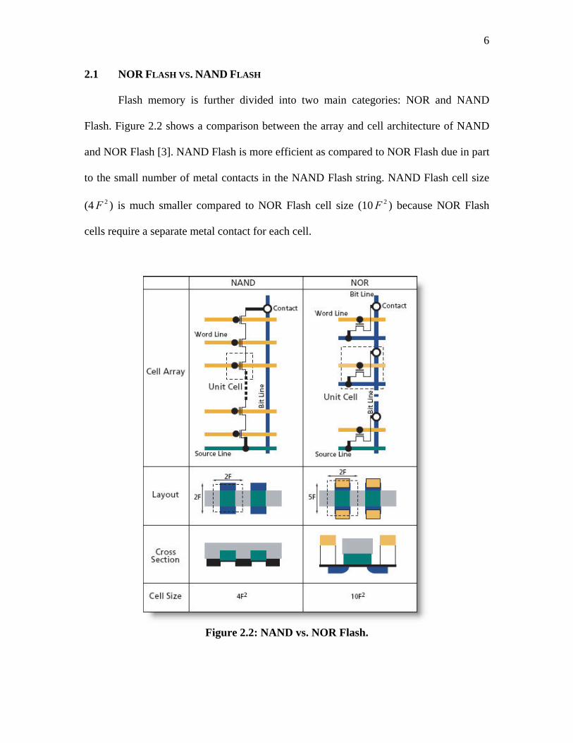
2.1 NOR FLASH VS. NAND FLASH
Flash memory is further divided into two main categories: NOR and NAND
Flash. Figure 2.2 shows a comparison between the array and cell architecture of NAND
and NOR Flash [3]. NAND Flash is more efficient as compared to NOR Flash due in part
to the small number of metal contacts in the NAND Flash string. NAND Flash cell size
(4 ) is much smaller compared to NOR Flash cell size (10 ) because NOR Flash
cells require a separate metal contact for each cell.
2F 2F
Figure 2.2: NAND vs. NOR Flash.
7
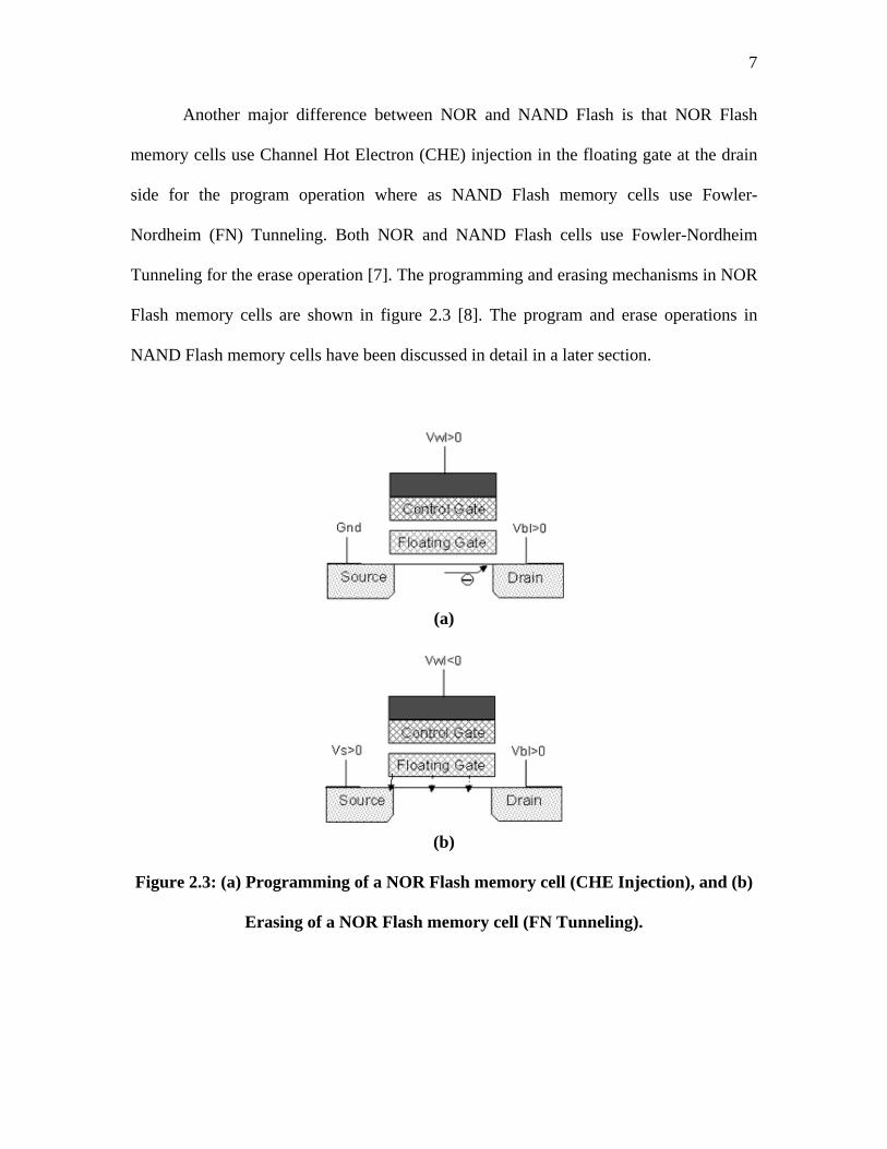
Another major difference between NOR and NAND Flash is that NOR Flash
memory cells use Channel Hot Electron (CHE) injection in the floating gate at the drain
side for the program operation where as NAND Flash memory cells use Fowler-
Nordheim (FN) Tunneling. Both NOR and NAND Flash cells use Fowler-Nordheim
Tunneling for the erase operation [7]. The programming and erasing mechanisms in NOR
Flash memory cells are shown in figure 2.3 [8]. The program and erase operations in
NAND Flash memory cells have been discussed in detail in a later section.
(a)
(b)
Figure 2.3: (a) Programming of a NOR Flash memory cell (CHE Injection), and (b)
Erasing of a NOR Flash memory cell (FN Tunneling).

8
Advantages and disadvantages of NOR Flash [3]:
The primary advantage of NOR Flash is fast random access which makes it ideal
for program code storage. Random access gives NOR Flash its execute-in-place (XiP)
functionality (code execution), which is often required in embedded applications.
However, an increasing number of processors include a direct NAND Flash interface and
can boot directly from the NAND Flash device (without NOR Flash). Another advantage
of NOR Flash is its byte write capability. A few of the most popular applications of NOR
Flash today include BIOS, Mobile Phones, Routers, Set-Top Boxes, and Video Games.
The main disadvantage of NOR Flash is its slow program and erase performance.
Another significant disadvantage of NOR Flash is the high programming current (since
CHE programming is used) [7].
Advantages and disadvantages of NAND Flash [3]:
The most prominent advantage of NAND Flash memory over NOR Flash is its
faster program and erase times. Moreover, NAND Flash cells are 60% smaller as
compared to NOR Flash cells providing higher densities required for today’s low-cost
consumer devices in a significantly reduced die area. NAND Flash typically incorporates
a string of 32 cells per contact in contrast with one contact per every cell in NOR Flash.
This results in smaller cells, and greater bit density at a lower cost. The fast program and
erase times, lower cost per bit, and small size make NAND Flash ideal for large amount
of data storage e.g. hard drives for personal computers. NAND Flash is very similar to a
hard disk drive. It is sector-based (page-based) and well suited for storage of sequential
data such as pictures, video, audio, or PC data. NAND Flash is used in virtually all
9
removable cards, including USB drives, secure digital (SD) cards, memory stick cards,
CompactFlash® cards, and multimedia cards (MMCs). The NAND Flash multiplexed
interface provides a consistent pinout for all recent devices and densities. This pinout
allows designers to use lower densities and migrate to higher densities without any
hardware changes to the printed circuit board. Other important applications of NAND
Flash memory include Mobile Phones, Digital Audio/Voice, Still & Video Cameras,
Mass Data Storage, and PDAs.
The main drawback of NAND Flash is its slower random access as compared to
NOR Flash. A comparison of basic advantages, disadvantages and applications of NAND
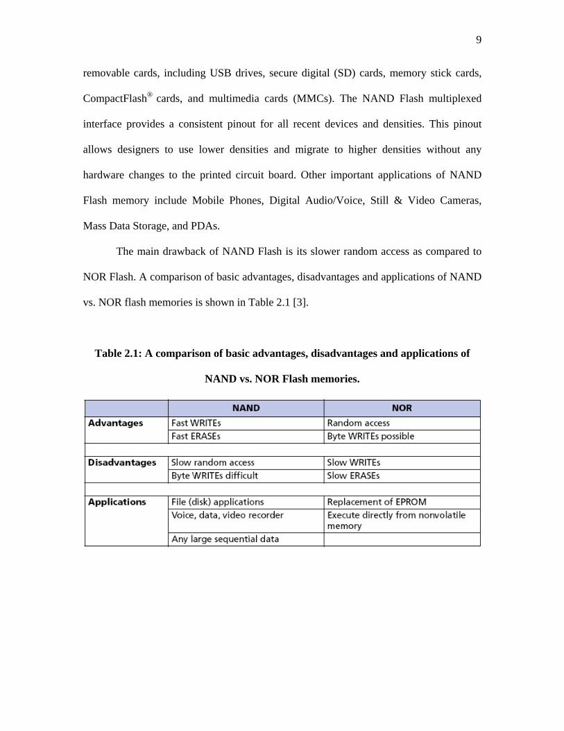
vs. NOR flash memories is shown in Table 2.1 [3].
Table 2.1: A comparison of basic advantages, disadvantages and applications of
NAND vs. NOR Flash memories.

10
2.2 CELL STRUCTURE OF THE NAND FLASH MEMORY CELL
The basic structure of a NAND Flash memory cell is similar to that of a
MOSFET, as shown in figure 2.4. It is composed of a dual-gate transistor. The dual-gate
functionality allows charge storage on the floating gate and thereby alteration of the
device threshold voltage (threshold voltage modulation). This enables programming and
erasing the transistor by adding or removing charge from the floating gate in order to
produce distinct logical values.
Figure 2.4: Basic structure of a NAND Flash memory cell.

11
The various components of a NAND Flash memory cell and their respective
functions are as follows:
• Gate Oxide: The gate oxide is also often referred to as “tunnel oxide” and has two
primary functions:
o It is used to tunnel electrons during the “program” and “erase” operations.
The thickness of the oxide determines the tunneling current density.
o It determines the threshold voltage of the cell during the “read” operation.
• Floating Gate: A polysilicon layer that is completely surrounded by a dielectric
used to store charge and alter the threshold voltage of the device.
• Dielectric: This is simply an insulator, typically ONO (Oxide Nitride Oxide). The
function of this dielectric is to inhibit charge stored on the floating gate from
leaking into the control gate.
• Control Gate: The conductor of the wordline used to access the transistor.
A 3D view of a typical NAND Flash memory cell is shown in figure 2.5 [9].
Figure 2.5: 3D view of a typical NAND Flash memory cell.

12
Scann AND Flash
memor
ing Electron Microscope (SEM) cross-sections of typical SLC N
y cells is shown in figure 2.6 [4].
Figure 2.6: Scanning electron microscope (SEM) cross-sections of typical SLC
ince the floating gate is electronically isolated, voltage can not be directly
applied
NAND Flash memory cells.
S
to it. A fraction of the voltage applied to the control gate is “seen” by the floating
gate due to capacitive coupling. In other words, capacitive coupling is used to indirectly
control the floating gate. The voltage seen by the floating gate then plays its role in
bending the energy bands at the Floating Gate-Tunnel Oxide interface. The voltage seen
by the floating gate in a Flash memory cell is analogous to the voltage applied to the gate
of a MOS transistor. The gate stack of a Flash Memory cell can be thought of as two
capacitors in series as shown in figure 2.7.

13
Figure 2.7: Gate stack of the Flash memory cell can be replaced by capacitors in
series to understand the effect of capacitive coupling.
The basic capacitive components of the Flash memory cell and respective
calculations are further discussed in the next section.
2.3 PRINCIPLES OF OPERATION OF THE NAND FLASH MEMORY CELL
Flash Memory stores information in an array of transistors also called ‘cells’.
Figure 2.8 shows the schematic view of a conventional NAND Flash memory array.
Wordline
Control Gate Floating Gate
Bitline
Figure 2.8: Schematic view of a conventional NAND Flash memory array structure.
14
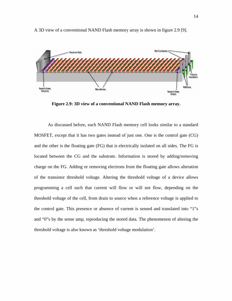
A 3D view of a conventional NAND Flash memory array is shown in figure 2.9 [9].
Figure 2.9: 3D view of a conventional NAND Flash memory array.
s discussed before, each NAND Flash memory cell looks similar to a standard
MOSFE
A
T, except that it has two gates instead of just one. One is the control gate (CG)
and the other is the floating gate (FG) that is electrically isolated on all sides. The FG is
located between the CG and the substrate. Information is stored by adding/removing
charge on the FG. Adding or removing electrons from the floating gate allows alteration
of the transistor threshold voltage. Altering the threshold voltage of a device allows
programming a cell such that current will flow or will not flow, depending on the
threshold voltage of the cell, from drain to source when a reference voltage is applied to
the control gate. This presence or absence of current is sensed and translated into “1”s
and “0”s by the sense amp, reproducing the stored data. The phenomenon of altering the
threshold voltage is also known as ‘threshold voltage modulation’.

15
Figure 2.10: Threshold voltage modulation.
As shown in figure 2.10, the threshold voltage of the Flash Memory Cell is altered
or “modulated” simply by adding or removing electrons from the floating gate.
Figure 2.11 shows the distributions of programmed (“0”) vs. erased (“1”) cells
in an array.
TV
Figure 2.11: distributions of programmed (“0”) vs. erased (“1”) cells in an array. TV
Some modern Flash memory devices, referred to as multi-level cell (MLC)
devices, can store more than 1 bit per cell (typically 2 bits per cell for current technology)
by varying the number of electrons placed on the FG, as compared to single-level cell

16
(SLC) devices that can store only one bit per cell at a time. In other words, in MLC
devices, one threshold voltage level represents two bits. Figure 2.12 shows the
distributions in MLC devices. TV
Figure 2.12: distributions in MLC devices. TV
However, since the delta between each state is decreased in MLC devices
compared to SLC devices, the margins between the threshold voltages of subsequent
logic states is significantly reduced. Thus, more rigidly controlled programming is
needed to manipulate a more precise amount of charge stored on the floating gate. At the
same time, precise charge sensing is required as well.
Multi-level cell devices have some advantages and some disadvantages over
single-level cell devices. The basic advantages of each of the two types of Flash memory
cells have been summarized in table 2.2 [3].

17
Table 2.2: Basic advantages of SLC vs. MLC Flash devices.
SSLLCC MMLLCC High Density
Low Power Consumption Program/Erase Speeds
Program/Erase Endurance Low Cost per Bit
Operating Temperature Endurance
The threshold voltage shift, TVΔ , caused by charge stored on the floating gate of
a NAND Flash memory cell is given by [10],
IPDT C
qNV .=Δ (2.1)
where is the electronic charge, N is the number of electrons stored on the floating
gate, and
q
IPDC is the control gate to floating gate capacitance. is given by, IPDC
IPD
IPDIPD EOT
SC
.0ε= (2.2)
where is the equivalent oxide thickness of the interpoly dielectric (IPD) and
is the floating gate area covered by the control gate.
IPDEOT IPDS

18
The threshold voltage of the floating gate memory cell at any given time, , can
therefore be written as
TV
TTT VVV Δ+= 0 (2.3)
where is a constant that depends on the gate and substrate material, doping,
and gate oxide thickness. is given by the expression
0TV
0TV
ox
dm
ox
oxmsFT C
QCQ
V −−Φ+Φ= 20 (2.4)
where
FΦ is the Fermi potential of the substrate at the surface at inversion
msΦ is the work function difference between the gate metal and the substrate
oxQ is the fixed charge in the tunnel oxide
dmQ is the maximum charge held by the depletion layer at inversion
oxC is the capacitance of the tunnel oxide
It can be seen that the effective threshold voltage of the transistor can be altered
by changing the amount of charge stored on the floating gate i.e. altering the term. TVΔ
The basic operations performed on a Flash Memory Cell include reading,
programming, program inhibiting, program verifying, erasing, erase inhibiting, and erase
verifying. The mechanisms involved in reading, programming, program inhibiting,
erasing, and erase inhibiting an MLC device are essentially the same as for an SLC
device. For the reason of simplicity, the above mentioned basic operations are discussed
for the case of an SLC device.

19
A NAND Flash memory cell is programmed (set to a “0” state) by applying a
large voltage, , on the CG (Control Gate). provides an electric field strong
enough to tunnel electrons from the substrate to the FG (Floating Gate), through the
tunnel oxide. This process of field assisted tunneling is called Fowler-Nordheim (FN)
Tunneling. To erase the cell (reset to “1”), a large voltage differential, , is placed
between the substrate and the gate. provides an electric field strong enough to
tunnel electrons from the floating gate back to the substrate, through the tunnel oxide.
programV programV
eraseV
eraseV
The read, program, program inhibit, program verify, erase, erase inhibit, and erase
verify operations are subsequently discussed in detail.
• Read: The “read” operation is performed to determine whether the cell is in a
“programmed” (“0”) or “erased” (“1”) state. A reference voltage, , is applied to the
control gate, where < < . is the threshold voltage of an
erased cell and is the threshold voltage of a programmed cell.
readV
erasedTV − readV programmedTV − erasedTV −
programmedTV −
o Reading An erased cell (“1”): When the cell is in the un-programmed or “erased”
state, the floating gate is depleted of electrons. In order to read the cell, is
applied to the control gate and a source to drain voltage potential is also applied.
Since the floating gate in the erased state is depleted of electrons, the applied voltage
is sufficient to drive the cell into inversion, since < . The cell is now
turned “on” and there is a current flow from drain to source that is sensed by the
sense amp and the cell is read as a “1“.
readV
erasedTV − readV
20
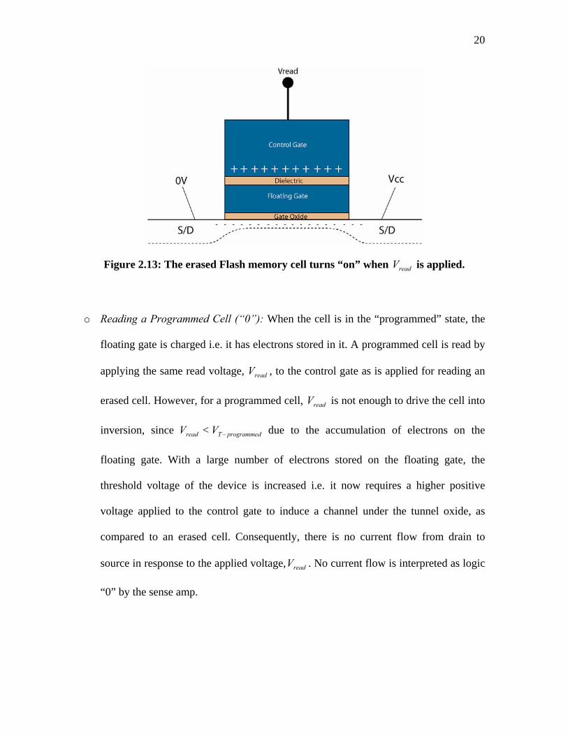
Figure 2.13: The erased Flash memory cell turns “on” when is applied. readV
o Reading a Programmed Cell (“0”): When the cell is in the “programmed” state, the
floating gate is charged i.e. it has electrons stored in it. A programmed cell is read by
applying the same read voltage, , to the control gate as is applied for reading an
erased cell. However, for a programmed cell, is not enough to drive the cell into
inversion, since < due to the accumulation of electrons on the
floating gate. With a large number of electrons stored on the floating gate, the
threshold voltage of the device is increased i.e. it now requires a higher positive
voltage applied to the control gate to induce a channel under the tunnel oxide, as
compared to an erased cell. Consequently, there is no current flow from drain to
source in response to the applied voltage, . No current flow is interpreted as logic
“0” by the sense amp.
readV
readV
readV programmedTV −
readV

21
Figure 2.14: The programmed Flash memory cell is “off” when is applied. readV
An SLC Flash memory device is engineered such that it has two statistical
distributions of threshold voltages in the array (i.e. for programmed and erased cells).
Figure 2.15 shows the distributions of acceptable ranges for ’s of programmed (“0”)
and erased (“1”) cells.
TV
Figure 2.15: Distributions of acceptable ranges for the ’s of programmed (“0”)
and erased (“1”) cells.
TV

22
As seen in figure 2.15, sits between the two distributions of threshold
voltages. This is done so that if the cell has not been programmed, will induce a
conductive channel allowing current flow from drain to source and is interpreted as a “1”
stored in the cell.
readV
readV
At the same time, is smaller than the ’s of the programmed distribution,
therefore there is no current flow from drain to source and is interpreted as a “0” stored in
the cell.
readV TV
The effect of electrons stored on the floating gate on the threshold voltage of the
cell can be expressed by the following equation [11]:
IPD
FGerasedTprogrammedT C
QVV −= −− (2.5)
where
erasedTV − is the threshold voltage of an erased cell.
programmedTV − is the threshold voltage of a programmed cell.
FGQ is the charge stored on the floating gate.
IPDC is the interpoly dielectric capacitance or the control gate to floating gate
capacitance.
A simplified schematic energy band diagram of an erased (left) and a
programmed (right) Flash memory cell are shown in figure 2.16 [8].

23
Figure 2.16: Energy band diagram of an erased (left) and a programmed (right)
Flash memory cell.
• Program: Programming or “writing” to an un-programmed cell simply means charging
the floating gate. This is done using Fowler-Nordheim Tunneling. A large positive
voltage, , is applied to the control gate while the substrate is grounded. When the
oxide barrier between the substrate and the floating gate becomes thin enough, electrons
tunnel from the substrate to the floating gate through the gate oxide. Fowler-Nordheim
Tunneling has been discussed in detail in a later section.
programV

24
Figure 2.17: Voltage conditions during programming a NAND Flash memory cell.
• Program Inhibit: The programming voltage that is applied to the selected wordline is
carried to all cells sharing the wordline. If a high potential such as is applied
to the wordline, all cells sharing the wordline would get programmed rather than just
the selected cell. In order to prevent unselected cells from being programmed, they
must be “inhibited” from being programmed. The program inhibit process is also
often referred to as “boosting”.
programV

25
Before proceeding to a detailed explanation of the process of boosting, the
following device parameters are assumed for the purposes of demonstration:
=CCV 1.8V
TV of SGD and SGS = 0.8V
=passV 5V
=inhibitV 10V
=programV 20V
The following are the basic steps involved in the boosting process:
o Step 1: The SGD voltage is driven to (1.8V) and all wordlines to . This
opens a continuous channel from the bitline down the length of the string. The
unselected bitlines (all strings except for the ones in which the cell to be programmed
exists) are ramped to (1.8V). The selected bitline (string in which the cell
selected for programming exists) is kept grounded. The cells in the unselected strings
are now off and the channels floating at ~1V (1.8V-
CCV passV
CCV
TV ), while the channels of the
cells in the selected string are still at 0V. The source slot is ramped to . This stops
current from flowing through the string. Since no current is flowing, but all channels
are open, the source, drain, and channel of all cells in the string will be at the same
potential. Figure 2.18 (a) shows the cell conditions after step 1 of the boosting process
[9].
CCV

26
o Step 2: The potential on SGD is dropped from 1.8V to 1.0V. Since the of these
cells is 0.8V, this guarantees that the SGD transistor of all unselected strings are shut
off ( < or 1.0V-1.8V<0.8V), while the SGD of selected strings remain on
( > or 1.0V-0V>0.8V). The source, drain and channel of the unselected strings
are therefore floating, while those of the selected string still have a path to ground.
Figure 2.18 (b) shows the cell conditions after step 2 of the boosting process [9].
TV
GSV TV
GSV TV
o Step 3: All wordlines in the block are raised to 10V ( ). The floating channels of
the unselected strings will capacitively couple to the gate and float up to
approximately 8-9V, thereby reducing the gate-to-well potential to approximately 10-
12V. That is not enough potential to induce tunneling, so these cells will not be
programmed. The selected wordline is then raised to 20V. Since the selected string is
still grounded, the gate-to-well potential on the selected wordline is 20V, while the
potential across the cells on the unselected wordlines is only 10V. Therefore, only
the cell on the selected wordline and bitline will be programmed. Figure 2.18 (c)
shows the cell conditions after step 3 of the boosting process [9].
inhibitV

27
(a)
(b)

28
(c)
Figure 2.18: Cell conditions after (a) step 1 of the boosting process, (b) step 2 of the
boosting process, (c) step 3 of the boosting process.
Figure 2.19 shows a final cell conditions at the end of the boosting process.
Figure 2.19: Final cell conditions at the end of the boosting process.

29
A cross-section view and respective voltage conditions within a selected (5 cell)
string are shown in figure 2.20 [9].
Figure 2.20: Cross-section view and respective voltage conditions within the selected
string.
A cross-section view of a program inhibited (5 cell) string and the respective
voltage conditions is shown in figure 2.21 [9].
Figure 2.21: Cross-section view and respective voltage conditions within a program
inhibited string.

30
A timeline of the boosting process is shown in figure 2.22 [9].
Figure 2.22: A timeline of the boosting process.
It must be noted that even though the representations above show 20V being
applied as the programming voltage, in modern NAND Flash devices, program verify
operations (discussed later in this section) are performed at fixed intervals during the
ramping of the wordline to 20V. In other words, the applied program pulses are ramped
up starting from a small voltage and increased gradually, with program verify operations
performed intermittently. The single cell programming algorithm can be broken down
into the following steps:
31
1. Apply a low voltage program pulse to the selected wordline (and, in turn, to the
selected gate).
2. Check the cell (Program Verify operation). TV
3. If cell ≥ Target , end programming loop. TV TV
4. If the cell < Target , increment the gate voltage (stepped WL voltage). TV TV
5. Repeat steps 2-3.
In summary, the starting gate voltage needs to be low enough to ensure the cell
does not over program in the first pulse. The key to programming a cell, without over-
programming the selected cell, is to move the threshold voltage up as gently as possible
yet hard enough to minimize the time to program. Another reason for not applying higher
than necessary program pulse voltage is to avoid inadvertently programming neighboring
cells (‘Program Disturb’ mechanism).
• Program Verify: After the program operation, a program verify is done with slight guard
band. That means that we apply slightly higher voltage to the wordline than a typical read
operation to guarantee margin. This voltage is known as the program verify voltage, .
Each sense amp tries to detect the state of the cell in a program verify operation.
Internally, the sense amp maintains a latched state of the expected data and does a
compare vs. the sensed data.
pvV
If the cell in question has been “programmed” enough, it will have a
greater than , and no current flow will be detected by the sense amp and the cell is
read as a “0”. On the other hand, if the of the cell in question is below the
TV
pvV
TV

32
expected , and the string discharges, the sense amp will detect the current
and the cell is read a “1”, which indicates the program operation has not completed
yet. Another program pulse is then applied to the cell followed by another program
verify operation. This algorithm is repeated until the cell in question is verified to
have been programmed or we have a program verify failure (program fail status).
programmedTV −
• Erase: Erasing a programmed cell is the reverse process of programming an erased cell,
i.e. instead of tunneling electrons from the substrate to the floating gate, we now tunnel
electrons from the floating gate back to the substrate. A sufficiently large positive
voltage, , is applied to the substrate while the control gate is grounded and electrons
tunnel from the floating gate to the substrate through the gate oxide, again, by the process
of Fowler-Nordheim tunneling.
eraseV
Figure 2.23: Voltage conditions during erasing a NAND Flash memory cell.
33
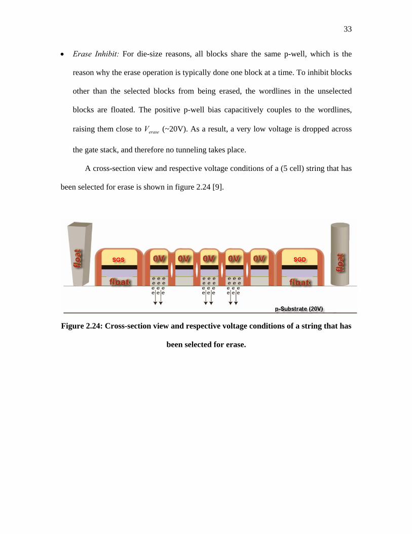
• Erase Inhibit: For die-size reasons, all blocks share the same p-well, which is the
reason why the erase operation is typically done one block at a time. To inhibit blocks
other than the selected blocks from being erased, the wordlines in the unselected
blocks are floated. The positive p-well bias capacitively couples to the wordlines,
raising them close to (~20V). As a result, a very low voltage is dropped across
the gate stack, and therefore no tunneling takes place.
eraseV
A cross-section view and respective voltage conditions of a (5 cell) string that has
been selected for erase is shown in figure 2.24 [9].
Figure 2.24: Cross-section view and respective voltage conditions of a string that has
been selected for erase.

34
The voltage conditions of a string that has been erase inhibited are shown in
figure 2.25 [9].
Figure 2.25: Voltage conditions of an erase inhibited string.
P-Substrate+20V
BL = float
float
float
float
float
Coupled to 20V
P-substrate = 20V
float
• Erase Verify: Erase verify is not performed cell-by-cell as opposed to a program
verify. Instead, each string is verified, with all wordlines set to Erase Verify voltage,
. If the string current detected by the sense amp is lower than the expected current
(i.e. the current when all cells in the string are erased), it indicates that one or more
cells in the string have not been completely erased. More erase pulses are then
applied followed by another erase verify. This algorithm is repeated until all cells in
the string are verified to have been erased or we have an erase verify failure (erase
fail status).
evV

35
Figure 2.26 shows the distribution of programmed vs. erased cells, in an SLC
device, relative to , , , and .
TV
evV readV pvV passV
Figure 2.26: distribution of programmed vs. erased cells relative to , , , and .
TV evV readV pvV
passV
The relative characteristics and conditions of programmed and erased cells in an
SLC device have been summarized in table 2.3.
Table 2.3: Relative cell conditions of programmed vs. erased cells in an SLC device.
Cell state # of e-‘s in Floating Gate Cell VTCurrent in Channel
(when Vread is applied)? Logic State
Not Programmed Low Low Yes 1
Programmed High High No 0
36
The electronic characteristics of a Flash memory cell are essentially like those of
a MOSFET. Once the potential of the floating gate is determined, the current equations
for a MOS transistor can be used to compute the IV characteristics of the Flash memory
cell [12].
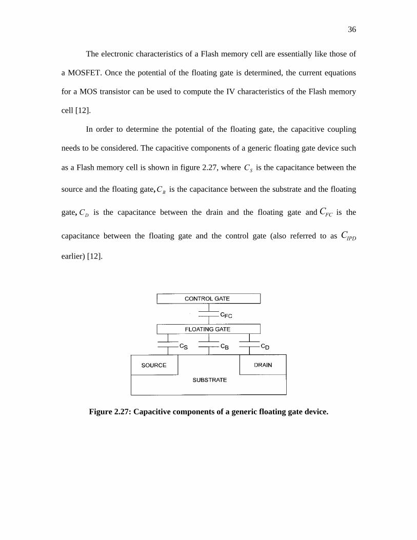
In order to determine the potential of the floating gate, the capacitive coupling
needs to be considered. The capacitive components of a generic floating gate device such
as a Flash memory cell is shown in figure 2.27, where is the capacitance between the
source and the floating gate, is the capacitance between the substrate and the floating
gate, is the capacitance between the drain and the floating gate and is the
capacitance between the floating gate and the control gate (also referred to as
SC
BC
DC FCC
IPDC
earlier) [12].
Figure 2.27: Capacitive components of a generic floating gate device.

37
As can be seen from figure 2.27, the total capacitance of the floating gate, , is
the sum of the individual capacitive components i.e.
TotalC
FCDBSTotal CCCCC +++= (2.6)
The total charge on the floating gate, , can then be written as
=
FGQ
FGQ FCCGFCDDFGBBFGSSFG CVVCVVCVVCVV ×−+×−+×−+×− )()()()( (2.7)
where is the potential on the floating gate, is the potential on the control gate,
and , , and are potentials on source, substrate, and drain, respectively. The
potential of the floating gate is given by
FGV CGV
SV BV DV
FGV = Total
FG
CQ
+ GSGVα + DSDVα + SSVα + BBVα (2.8)
where
Total
FCG C
C=α , the coupling coefficient relative to the control gate (2.9)
Total
DD C
C=α , the coupling coefficient relative to the drain (2.10)
Total
SS C
C=α , the coupling coefficient relative to the source (2.11)
Total
BB C
C=α , the coupling coefficient relative to the source (2.12)
Due to its near identical structure and function as a MOS transistor, the current-
voltage equations for a Flash memory cell can be derived from the current-voltage
equations of the MOS transistor. This is done replacing the MOS gate voltage with GSV
38
the floating gate voltage and transforming the device parameters such as threshold
voltage ( ) and conductivity factor (
FGV
TV β ), to values measured with respect to the control
gate [12]. If we define for =0, DSV
FGTV = Gα
CGTV (2.13)
and
=FGβ CG
G
βα1 , (2.14)
the current–voltage (I–V) equations of a floating gate transistor can be compared to
those of a conventional MOSFET in the triode region and the saturation region. The
derived current-voltage equations for a Flash memory cell are as follows:
In the triode region,
CGTDSGSGDS VfVVV −+< α (2.15)
and
=DSI CGβ ( ) ⎥⎦
⎤⎢⎣
⎡⎟⎟⎠
⎞⎜⎜⎝
⎛−−− 2
21
DSG
DSCG
TGS VfVVVα
(2.16)
In the saturation region,
CGTDSGSGDS VfVVV −+≥ α (2.17)
and
( )22
CGTDSGSG
CG
DS VfVVI −+= αβ (2.18)
where
⎟⎟⎠
⎞⎜⎜⎝
⎛==
FC
D
G
D
CC
fαα (2.19)

39
2.4 ELECTRICAL CONDUCTION THROUGH THIN DIELECTRICS
Electrical conduction through dielectrics can be divided into two main categories:
bulk-limited conduction and electrode-limited conduction [5]. In bulk limited conduction,
the electrical current is determined by the properties and characteristics of the dielectric
itself, and is independent of the characteristics of the electrodes where the current is
originating from. On the other hand, in electrode-limited conduction, the current is
determined by the properties and characteristics of the electrodes where the current is
originating from [13]. In the case of , the conduction current is electrode-limited.
That is because of the very large energy barrier of about 9eV and a high energy barrier of
about 3.2eV at its interface with silicon. An example of bulk-limited conduction can be
seen in the case of which has an energy gap of only about 5eV and an energy
barrier of 2eV at its interface with silicon. Another point to be noted is that since
has a smaller barrier for electrons in the conduction band (~3.2eV) compared to the holes
in the valence band (~4.7eV), the current through will be composed primarily of
electron conduction [5].
2SiO
43 NSi
2SiO
2SiO
The proof that the current through is electrode limited was observed by
Lezlinger et al. by studying the current-voltage characteristics of different electrode
materials [13]. For a metal-oxide-silicon system, it was observed that for a positive bias
on the metal, the current was independent of the metal used. At the same time, for a
negative bias on the metal, the current was dependent on the particular metal used.
2SiO
However, it has been shown in a study [14] that in an oxide containing a high
density of charge traps, the conduction process can change from being electrode-limited

40
to being bulk-limited. Charge trapping is a form of oxide degradation that may be caused
by high electronic field/current stress during the tunneling process.
Figure 2.28: Energy band diagram for the 2SiOSi − interface.
2.4.1 FOWLER-NORDHEIM TUNNELING
Fowler-Nordheim tunneling is a field-assisted electron-tunneling mechanism [5].
It is the tunneling of electrons from the vicinity of the electrode Fermi level through the
forbidden energy gap into the conduction band of the oxide in the presence of a high
electric field [13]. Fowler-Nordheim tunneling is one of the most important injection
mechanisms used in floating gate devices.
Due to the high electric field, the electrons in the conduction band of silicon see a
steep triangular energy barrier as shown in figure 2.29. The magnitude of the barrier
slope is directly proportional to applied electric field. The width of the energy barrier is,
therefore, determined by the applied electric field. The height of the barrier is determined
by the electrode material and the band structure of . As the electric field is increased 2SiO

41
by increasing the applied voltage at the control gate, the barrier slope becomes steeper
and hence the barrier width is decreased.
Figure 2.29: Energy band representation of Fowler-Nordheim tunneling through
thin oxides.
At sufficiently high fields, the width of the barrier becomes sufficiently small for
the electrons to tunnel through the barrier from the silicon conduction band into the oxide
conduction band [5]. In the Fowler-Nordheim regime, the value of the oxide electric field
becomes larger thanox
b
tΦ
, where bΦ is the barrier height and is the thickness of the
tunnel oxide [16]. This mechanism was originally demonstrated by Fowler and Nordheim
for electrons tunneling through a vacuum barrier and a modified version of that was later
presented by Lezlinger and Snow for oxide tunneling. The Fowler-Nordheim current
density is given by the following equation [5]:
oxt

42
)exp(2
inj
Cinj E
EEJ
−= α (2.20)
with
*
3
8 mm
hq
bΦ=
πα (2.21)
and
qmE b
Ch3
242
3* Φ= (2.22)
where = Plank’s constant ( ) h seV .104.13567 -15×
= The energy barrier at the injecting interface (3.2eV forbΦ 2SiOSi − )
= The electric field at the injecting interface (V/cm) injE
q = Electronic charge (- ) C1910602.1 −×
m = The mass of a free electron ( ) kg3110109.9 −×
= The effective mass of an electron in the band gap of (0.42m [17]) *m 2SiO
h =π2h

43
The I-V characteristic of Fowler-Nordheim tunneling is shown in figure 2.30 [18].
It can be seen that the current density is approximately exponentially dependent on the
electric field within the oxide.
Figure 2.30: Fowler-Nordheim tunneling I-V characteristics.
The energy band representation of the Floating Gate (polysilicon)-Tunnel Oxide
( )-Substrate ( ) system for a Flash memory cell at zero bias is shown in figure
2.31(a). The energy band representations of the Floating Gate (polysilicon)-Tunnel Oxide
( )-Substrate ( ) system during the program and erase operations are shown in
figures 2.31(b) and 2.31(c), respectively.
2SiO Si
2SiO Si
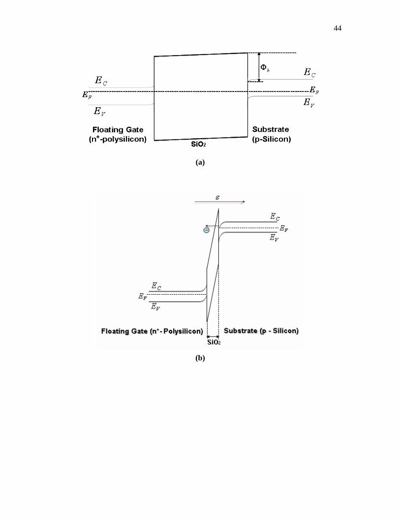
44
(a)
(b)

45
(c)
Figure 2.31: Energy band representation of Fowler-Nordheim tunneling (a) at zero
bias, (b) from substrate to floating gate (Program Operation), and (c) from floating
gate to substrate (Erase Operation).
It is important to note that at very high voltages, the silicon surface will be
degenerate n-type regardless of the bulk doping [13]. For an electrode with donor density
of and an oxide electric field of 7.5 MV/cm at the interface, the Fermi level
is calculated to be about 0.25eV above the bottom of the silicon conduction band at the
surface [15].
317105 −× cm

46
Summary:
This chapter reviewed the two types of semi-conductor memories i.e. volatile
semiconductor memory and non-volatile semiconductor memory while focusing on non-
volatile semiconductor memory, Flash in particular. The basic differences between NOR
Flash and NAND Flash, their respective advantages and disadvantages, and applications
were briefly discussed. Finally, a detailed discussion of the structure and function and
principles of operation of the NAND Flash memory cell were included in this chapter.
47
CHAPTER 3: RELIABILITY ISSUES IN NAND FLASH MEMORY
Despite its numerous advantages, Flash memory suffers from the disadvantage of
limited endurance [19]. There is a limit to the number of times the memory cells can be
programmed and erased. High electric fields and, in turn, high current densities are
applied to the tunnel oxide ( ) during the program/erase cycling of a Flash memory
cell. Program/erase cycling is known to cause a fairly uniform wear-out of the cell
performance, mainly due to tunnel oxide degradation, which eventually limits the
endurance characteristics [20]. The intrinsic limitation of the tunnel oxide to withstand
the high field/current induced stress is of significant importance as it directly translates to
the endurance and reliability of the cell. The reliability and performance of a Flash
memory cell are evaluated using device characteristics such as transient characteristics,
endurance characteristics and retention characteristics [5].
2SiO
The transient characteristics of a Flash memory cell include the shifting of the cell
threshold voltage (threshold voltage modulation) as a function of time during
programming and erasing. These characteristics, in turn, determine the values of the
voltages and the time needed to program and erase the cell. The cell threshold voltage
and, in turn, the program and erase time is altered by charge trapping in the tunnel oxide
caused by the tunneling current passing through it during the program and erase
operations.
The endurance of a Flash Memory cell is defined as the number of program and
erase cycles that can be performed before the device breaks down due to damage or
degradation of the tunnel oxide (owed to high field/current stress during Fowler-

48
Nordheim tunneling). Tunnel oxide degradation caused by Fowler-Nordheim tunneling
has been discussed in detail in a later section.
The retention of a Flash Memory Cell is defined as the time it takes for the charge
stored on the floating gate to be lost through leakage. The retention characteristic of a
Flash Memory cell is, again, dependent on tunnel oxide degradation caused by Fowler-
Nordheim tunneling during programming and erasing.
The combined effect of all the device characteristics i.e. transient, endurance, and
retention define the reliability and performance of a Flash memory cell. Moreover, as
mentioned before, these characteristics are strongly dependent on tunnel oxide
degradation caused by high field/current induced stress during Fowler-Nordheim
tunneling.
3.1 TUNNEL OXIDE DEGRADATION CAUSED BY FOWLER-NORDHEIM TUNNELING
Charge trapping in tunnel oxide caused by Fowler-Nordheim tunneling is one of
the main causes of degradation in Flash memory cells and therefore one of the limiting
factors in their long-term reliability [15]. Tunnel oxide degradation in a Flash Memory
cell is much more significant as compared to a typical MOSFET because of the high
field/current induced stress during Fowler-Nordheim tunneling. A typical Flash Memory
cell is operated at voltages as high as 20V which is considerably higher as compared to
the operating voltages of a typical MOSFET.
One of the most significant tunnel oxide degradation mechanisms is stress-
induced charge trapping. Charge trapping is directly correlated to the threshold voltage
shift during program/erase cycles in Flash memory cells [21] which leads to memory
49
window ( ) narrowing eventually causing the cell to reach
end of its life-time. Charge traps are storage sites for electrons or holes in the oxide
created due to degradation caused by high field/current induced stress during Fowler-
Nordheim tunneling.
TVΔ erasedprogrammedT VVV −=Δ
Charge trapping in the tunnel oxide causes transient, endurance and retention
failures in Flash memory cells and therefore is an important phenomenon to understand
in order to attempt improving the reliability and endurance of Flash memory cells.
3.1.1 CHARGE TRAPPING IN TUNNEL OXIDE
Charges in systems can be broken down into four main categories [22]: 2SiOSi −
1- Interface trapped charge: This is the charge that is located at the
interface. These are attributed to intrinsic dangling bonds, oxidation induced structural
defects, and physically induced defects.
2SiOSi −
2- Fixed oxide charge: This is the charge located in the oxide near the
interface and is primarily positively charged. This charge originates from the oxidation
process in which ionized silicon is not satisfied with an oxygen bond.
2SiOSi −
3- Oxide trapped charge: This is the charge located in the bulk of the oxide and can be
negatively or positively charged, depending on the polarity of the charge trapped.
4- Mobile ionic charge: This type of charge occurs mainly due to ionic contamination
such as Na+. A source of ionic contamination can be physical contact of the oxide with
human skin, which contains Na+ ions.
50
Among the above mentioned four categories, interface trapped charge and oxide
trapped charge play the most significant role, when it comes to Fowler-Nordheim
tunneling and reliability in Flash memory cells [22].
High field/current stressing during Fowler-Nordheim tunneling causes both
positive and negative charge trapping in [23]. The origin of charge traps is still not
entirely understood and is a current area of interest for researchers. There have been a
number of theories and models attempting to explain the phenomenon of charge trap
generation in . A few models are based on the relaxation of a bond close to the
interface after a hole is captured and others based on the effect of hydrogen liberated by
stress [15]. It is believed by researchers that trap generation is a consequence of Si-H
bond breaking by high energy electrons [24].
2SiO
2SiO
According to Jeno et al. [23], positive charge trapping is believed to be a
consequence of direct tunneling between the anode and the trap sites near the
interface and negative charge trapping is believed to be caused by the trapping of the
injected electrons into the traps that pre-exist in the oxide as well as the traps that are
generated during the high field/current stressing of the oxide. According to a study on
hole trapping in [25], it was suggested that during Fowler-Nordheim tunneling,
some of the high-energy electrons will generate electron-hole pairs in the oxide (by
impact ionization) and some of the generated holes will be trapped within the oxide. It
was reported in [26] that electron trap sites are related to diffused water into the
film, which is in compliance with the conclusions made in [24]. It was shown that
negative charge build-up in ultra-dry oxide is 1/10
2SiOSi −
2SiO
2SiO
th that of wet oxide. The results in [26]
suggest that the hydrogen contained in the oxide strongly affects the generation of

51
electron traps in as shown in figure 3.1, which are in compliance with the theories
and conclusions supported in [24].
2SiO
Figure 3.1: Electron trap density as a function of Hydrogen concentration in the
oxide.
In an experiment conducted by Jeno et al. [23], Polysilicon- -Si capacitors
were used to study high field/current stress induced charge trapping in . C-V and I-
V measurements were used to monitor the concentration as well as the centroid of the
charge build-up in the Polysilicon- -Si capacitors. Capacitors with p-type substrates
were subjected to high current stress for 10 seconds and the C-V and I-V measurements
that were obtained are shown in figure 3.2.
2SiO
2SiO
2SiO

52
(a)
(b)
Figure 3.2: (a) C-V and (b) I-V measurements before and after the Polysilicon-SiO2-
Si capacitors were stressed for a short time.
When gate stress was applied to the p-type capacitors, a negative shift in the C-V
curve was observed indicating a net positive charge in the oxide. From the shifts in C-V
i.e. + and I-V i.e. -, the centroid of the positive charges, VΔ VΔ +'X , was calculated
using the following equation:

53
+−
+=
+Δ−Δ
''Xd
XVV
ox
(3.1)
where +'X is measured from the 2SiOSi − interface. It was found that the value of +'X
was much smaller compared to the thickness of suggesting that the positive charges
are very close to the interface.
2SiO
2SiOSi −
It was further observed that the concentration of the positive charges (which can
be determined from the C-V or I-V shift using the calculated value of +'X ) is
independent of the oxide thickness and hence it is indeed an interface phenomenon.
Figure 3.3 shows the concentration of positive charges plotted against various stress
fields for different oxide thicknesses [23].
Figure 3.3: Positive charge concentration plotted against various stress fields for
different oxide thicknesses.
54
It was further observed that the concentration of trapped positive charges
increased exponentially with the applied stress field.
Overall, it was shown that positive charges are formed/trapped near the
interface as a consequence of direct tunneling between the anode and the trap sites near
the interface and that their concentration is independent of the thickness of the
oxide.
2SiOSi −
2SiOSi −
As discussed above, initially a negative shift (due to positive charge trapping ) of
the C-V curve is seen. However, it was observed that after a short duration of continuous
high field stress, the curve begins to shift in the positive direction and a net positive shift
is seen relative to the initial curve [23]. The obvious deduction is that as more and more
electrons get trapped in the oxide, the total number of negative charges trapped out
number the total number of positive charges and the oxide at which point the oxide
carries a net negative charge trapped.
In order to study the concentration and centroid of the negative charges trapped in
the oxide, it was made sure that the positive charges initially trapped in the oxide were
neutralized. One of the methods that can be used is to apply a reversed gate stress. An
initial set of positive and negative I-V curves were recorded. The I-V measurements were
made at relatively low current levels (at least two orders of magnitude lower than the
stressing current) to make sure a significant amount of electron trapping is not introduced
in the oxide. The Polysilicon- -Si capacitors were then stressed and positive and
negative I-V curves were taken. It was observed that (given the positive charges are
properly neutralized) the positive and negative I-V curves shifted by the same amount i.e.
+ = - , implying that the centroid of negative charges,
2SiO
VΔ VΔ −'X , is at the center of the

55
oxide. Figure 3.4 shows the positive and negative I-V curves taken before and after
stressing the capacitors for 10 minutes [23]. As in the case of positive charges, the
concentration of the negative charges can be determined from the C-V or I-V shift using
the calculated value of −'X .
Figure 3.4: Positive and negative I-V curves taken before and after the Polysilicon-
SiO2-Si capacitors were stressed for a prolonged period of time (10 minutes).
The phenomenon of initial net positive charge generation (hole trapping) followed
by a net negative charge generation in the oxide (electron trapping) was reconfirmed in a
study done by Ohij et al. [26]. It was shown that the leakage current in a constant current
stressing test of (oxynitrided and un-oxynitrided) silicon dioxide initially increased for a
short time and subsequently decreased confirming the initial generation of positive
charges and subsequent generation of net negative charges, as shown in figure 3.5. It can
be clearly seen that the phenomenon of the initial net positive charge generation is short-
lived and net negative charge trapping quickly becomes dominant.

56
Figure 3.5: Leakage current changes in a constant current stressing test of SiO2.
Impact ionization caused by high energy electrons generates electron-hole pairs in
the oxide and some of the holes get trapped in the oxide [25]. After the electron-hole
pairs are generated, they are free to tunnel through to the anode and cathode, respectively.
However, since has a smaller barrier for electrons in the conduction band (~3.2eV)
compared to the holes in the valence band (~4.7eV), a greater number of generated
electrons will tunnel through to the anode compared to the number of holes tunneling
through to the cathode [5]. According to [23], positive charges are generated in the oxide
by to direct tunneling between the oxide and the anode. However, the number of electron
traps in the oxide increases as the oxide degrades due to high field/current stressing of the
oxide until they out-number the positive charges and the oxide exhibits a net negative
charge trapping [23]. It was shown that trapped positive charges are relatively unstable
2SiO

57
compared to negative charges and can be easily neutralized. On the contrary, the trapped
electrons are much more stable, which explains the domination of electron traps in the
oxide in the long term. The energy level of trapped electrons is believed to be at least
more than 3.25eV below the conduction band of the . 2SiO
3.2 RELIABILITY CONCERNS CAUSED BY CHARGE TRAPPING IN TUNNEL OXIDE
The density of charge trapped in the oxide is proportional to the current density
integrated over time (flux) [27]. After repeated program and erase cycles over time, the
tunnel oxide traps up enough charge that the cell reaches the end of endurance. End-of-
life endurance by trap-up is a typical failure mode in Flash memory cells [5].
The typical endurance characteristics of an SLC NAND Flash memory cell are
shown in figure 3.6 [4]
Figure 3.6: SLC Flash memory cell endurance characteristics.
58
It can be seen that there is an increase in and with extended
program/erase cycling of the NAND Flash memory cells.
programmedTV − erasedTV −
As discussed before, there is an initial generation of net positive charge (holes) in
the tunnel oxide, however, that phenomenon is short-lived. An initial slight decrease in
may sometimes be observed as a consequence of the positive charge generation
in the tunnel oxide which enhances the tunneling efficiency [8,25,28], as shown in figure
4.4. The increase in net positive charge in the oxide, which results in an additional
electric field at the interface, causes additional electrons to be tunneled out from the
floating gate during the erase operation. At the same time, the positive charges in the
oxide result in a decrease in the intrinsic threshold voltage of the erased cell. The two
effects i.e. over-erasing of the cell (removal of more than intended electrons to the
floating gate) due to increase in tunneling efficiency and decrease of the intrinsic
threshold voltage of the cell due to positive charges in the oxide result in a decrease in
. On the other hand, during the program operation, the same phenomenon i.e. an
increase in the tunneling efficiency caused by the positive charges in the oxide results
additional electrons being tunneled into the floating gate. The over-programming of the
cell (addition of more than intended electrons to the floating gate) has an effect of
increasing the threshold voltage of the programmed cell. However, the positive charges in
the oxide have an effect of decreasing the intrinsic threshold voltage of the cell. Since the
two phenomena i.e. increase in tunneling efficiency and decrease in intrinsic threshold
voltage of the cell have an opposite effect, often little or no initial change in
is observed, as has been well explained in [28]. The net effect on (increase or
decrease) depends on which one of the two phenomena i.e. decrease in intrinsic threshold
erasedTV −
erasedTV −
programmedTV −
programmedTV −
59
voltage due to positive charge generation and increase in tunneling efficiency is
dominant. However, as mentioned earlier, the phenomenon of positive charge generation
in the oxide is short-lived (as seen in figure 4.4) and hence the change in and
may not always be detected, which is the case in endurance characteristics
shown in figure 3.6.
erasedTV −
programmedTV −
As the number of program/erase cycles increase, starts to rise. The long-
term increase in is due to the generation of net negative charge or traps in the
oxide [8]. During the erase operation, the increase in net negative charge in the oxide
results in a reduction in the effective electric field at the interface which hinders the
tunneling of electrons out of the floating gate during the erase operation. Also, the
negative charges in the tunnel oxide result in an increase in the intrinsic threshold voltage
of the cell. The two phenomena i.e. under-erasing of the cell (removal of less than
intended electrons from the floating gate) and increase in the intrinsic threshold voltage
of the cell result in an increase in . During the program operation, a decrease in
the tunneling efficiency caused by the negative charges in the oxide results in less than
intended electrons being tunneled out of the floating gate. The under-programming of the
cell (addition of less than intended electrons to the floating gate) has an effect of
decreasing the threshold voltage of the programmed cell. However, the negative charges
in the oxide have an effect of increasing the intrinsic threshold voltage of the cell.
Therefore, unlike the additive effect in the case of , the two phenomena i.e.
increase in the intrinsic threshold voltage and the reduction in tunneling efficiency
(caused by negative charge trapping) have an opposite subtractive effect on .
erasedTV −
erasedTV −
erasedTV −
erasedTV −
programmedTV −

60
That is the reason why the rise in is much sharper compared to the rise in
.
erasedTV −
programmedTV −
It must be noted that the endurance characteristics of NOR Flash memory cells
are slightly different as compared to NAND Flash memory cells. The difference is
essentially between the characteristics and is most likely due to the
difference in programming mechanisms between the two. NOR Flash memory cells
typically use CHE (Channel Hot Electron) injection mechanism to program the cells (as
opposed to FN tunneling used in NAND Flash memory cells) [7,28,29]. After extended
cycling, the degradation mechanism inherent to CHE programming appears. Interface
states generated at the drain side reduce the electron mean free path, impacting on the hot
carrier generation mechanism, and electrons trapped in the tunnel oxide modify the
electric field at the injection point, reducing the programming efficiency [28]. It can be
deduced that, in NOR Flash memory cells, the effect on reduction in CHE injection
efficiency caused by oxide degradation near the drain side is the dominant phenomenon
during the program operation (as compared to the affect of increase in intrinsic threshold
voltage caused by negative charge trapping).
programmedTV −
A typical endurance plot of a NOR Flash memory cell (using FN Tunneling for
erasing and CHE injection for programming) is shown in figure 3.7 [28]. Even though a
decrease in is not apparent until 100k cycles as seen in figure 3.7, an increase
in is seen when the cell is further cycled (which is equivalent to an increase in
when a program verify scheme is used) as shown in figure 3.9.
programmedTV −
programt
programmedTV −

61
Figure 3.7: Programmed and erased as a function of the number of cycles for a
cell under fixed program and erase conditions.
TV
The extent of change in in NOR Flash memory cells simply depends
on the how dominant one phenomenon is as compared to the other (i.e. reduction CHE
injection as compared to increase in intrinsic threshold voltage). On the other hand, in
NAND Flash memory cells, FN tunneling is used for both programming and erasing [7].
Therefore there is a uniform degradation of the tunnel oxide throughout the channel and
as the number of electrons traps increases with program/erase cycling, the intrinsic
threshold voltage of the cell increases. Since there is a net increase in both
and , it can be deduced that the increase in intrinsic threshold voltage has a
greater effect on the threshold voltage of the programmed and erased cells as compared to
the effect of reduction in tunneling efficiency caused by trapped electrons.
programmedTV −
programmedTV −
erasedTV −

62
The factors that make one phenomenon more than dominant than the other are
still not entirely understood and a topic of interest for many researchers. It has been
shown in a study [14] that in an oxide containing a high density of charge traps, the
tunneling process can change from being electrode-limited to being bulk-limited i.e. the
tunneling current starts to be dominated by the oxide characteristics as more and more
charge gets trapped in it. However, it is difficult to characterize the small differences in
endurance characteristics observed in different Flash memory cells. The presence and
generation of carriers of both polarities and diverse energies complicates the analysis and
determination of tunnel oxide degradation mechanisms.
Overall, the observed memory window behavior is restricted to the general
statement that memory window widening is caused by positive charge trapping and
memory window narrowing is caused by electron trapping [30,31,32].
As the number of program/erase cycles increases, the threshold voltage of erased
cells keeps increasing until it becomes too high for the sense amp to distinguish it from
programmed cells, as seen in figure 3.6. The memory window keeps decreasing until it
becomes smaller than the minimum acceptable margin value and the cell reaches end-of-
life.
In modern Flash memory devices, however, the threshold voltage shift and
window closure is compensated by means of program and erase verify schemes [28]. The
cell is checked after a program or erase operation (program/erase verify) in order to
determine whether or not the target has been achieved and, if not, programming or
erasing is continued until the cell is verified to have been programmed or erased. In
NAND Flash memory cells, where increases with P/E cycling when fixed
TV
TV
TV
programmedTV −

63
programming conditions are used (no program verify scheme), it is obvious that the cells
now require less than standard/initial programming to raise the threshold voltage to the
required (since standard programming conditions are raising the threshold
voltage to a value higher than that is required). That translates to a decrease in as
the number of P/E cycles increases when a program verify scheme is used. On the other
hand, the increase in with P/E cycling (when no erase verify scheme is used)
means that more than standard erase conditions (i.e. number of erase pulses/pulse
widths/pulse heights) are now required to lower the threshold voltage of the cell to an
acceptable level of . That translates to an increase in as the number of P/E
cycles increases. Figure 4.5 shows variability charts for the number of required program
and erase pulses (which directly translates to and ) as a function of
program/erase cycles for MLC NAND Flash memory cells fabricated on three different
silicon wafers. It can be seen that the number of erase pulses needed exponentially
increases after a certain number of P/E cycles as compared to a slight reduction in the
number of program pulses needed. It is obvious that the primary failure mechanism in
NAND Flash memory cells is erase verify failures i.e. becomes longer than the
device specification limit.
programmedTV −
programt
erasedTV −
erasedTV − eraset
programt eraset
eraset
On the other hand, as discussed before, in NOR Flash memory cells an increase in
and a decrease in is seen after extended cycling. That, of course,
translates to an increase in as well as . The program and erase times for a
NOR Flash memory cell as a function of the number of P/E cycles are shown in figure
3.8 [28].
erasedTV − programmedTV −
eraset programt

64
Figure 3.8: Program and erase times increasing as a function of number of
program/erase cycles in NOR Flash memory cells.
Similar results have been demonstrated in [8] where an increase in as well
as in NOR Flash memory cells was observed, shown in figure 3.9.
eraset
programt
Figure 3.9: Program and erase times increasing as a function of the number of
cycles.
It can be seen in figures 3.8 and 3.9 that, in NOR Flash memory cells, the rise in
is much sharper compared to the rise in with extended cycling (like in the
case of NAND Flash memory cells). That can again be attributed to the two phenomena
(increase in intrinsic threshold voltage and reduction in tunneling efficiency) having an
additive effect on as compared to the opposite effect on . Hence it can be
eraset programt
eraset programt
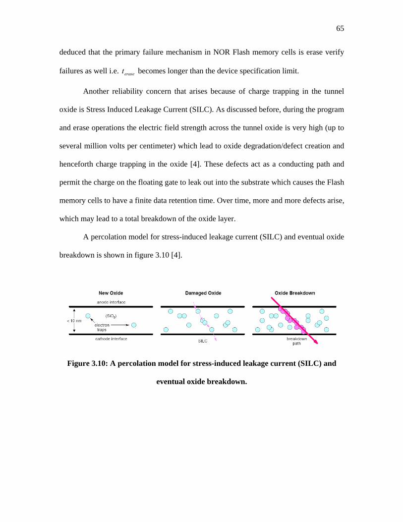
65
deduced that the primary failure mechanism in NOR Flash memory cells is erase verify
failures as well i.e. becomes longer than the device specification limit. eraset
Another reliability concern that arises because of charge trapping in the tunnel
oxide is Stress Induced Leakage Current (SILC). As discussed before, during the program
and erase operations the electric field strength across the tunnel oxide is very high (up to
several million volts per centimeter) which lead to oxide degradation/defect creation and
henceforth charge trapping in the oxide [4]. These defects act as a conducting path and
permit the charge on the floating gate to leak out into the substrate which causes the Flash
memory cells to have a finite data retention time. Over time, more and more defects arise,
which may lead to a total breakdown of the oxide layer.
A percolation model for stress-induced leakage current (SILC) and eventual oxide
breakdown is shown in figure 3.10 [4].
Figure 3.10: A percolation model for stress-induced leakage current (SILC) and
eventual oxide breakdown.

66
3.3 SOME PRIOR WORK FOR IMPROVING CHARGE TRAPPING IN TUNNEL OXIDE
Due to the importance and dire need of improving long-term reliability and
endurance of NAND Flash memory, it is a current topic of interest for many researchers.
Numerous methods have been proposed for improving charge trapping in tunnel oxide.
As discussed earlier, tunnel oxide degradation occurs primarily due to stress
induced traps created during Fowler-Nordheim tunneling [15]. A lot of work has been
done by researchers in attempt to improve charge trapping in tunnel oxide and, in turn,
the reliability and endurance of NAND Flash memory.
In a study done by Ohij et al. [26], it was revealed that electron trapping is
strongly related to the Si-OH or the Si-H bond in films, while hole trapping is
caused by oxygen vacancies in the , both origination from diffused water in the
oxide. It was also found that oxynitridation of film considerably reduces charge
trapping in the oxide during Fowler-Nordheim tunneling current injection, as shown in
figure 3.5. The oxynitrided gate dielectric therefore showed reduction in the
programming time degradation during the program/erase operations of the Flash memory
cells.
2SiO
2SiO
2SiO
2SiO
Similar results were observed in a study done by Fukuda et al. [21]. It was seen
that using rapid thermal oxynitridation (RTONO) shows significant reduction in the
memory window narrowing in Flash memory. In the RTONO technology proposed in
[21], the tunnel oxide is grown in three steps: Si is oxidized in at 1100 , then
lightly nitrided in ammonia ( ) at 900 , and then oxynitrided in nitrous oxide
( ) at 1100 . The RTONO technology showed a 42% reduction in memory
2O Co
3NH Co
ON 2 Co

67
window narrowing. According to another research, increasing annealing
temperature and time monotonically reduces electron trapping in the resulting oxides
[33]. The same results i.e. reduction in memory window closure caused by
annealing, have been demonstrated in [34], as seen in figure 3.12.
ON 2
ON 2
Figure 3.11: Reduction in memory window closure caused by N2O annealing.
-4
-2
0
2
4
6
8
10
1E+00 1E+01 1E+02 1E+03 1E+04 1E+05 1E+06 1E+07
P/E cycles
VT [
V]
Control
N2O annealed
Program Vth
Erase Vth
It was shown in [26] that the negative charges build up in the ultra-dry oxide is
1/10th that of the wet oxide. It was reported that the ultra-dry oxides give rise to excellent
interface immunities against Fowler-Nordheim stressing. That implies that
using ultra-dry oxide is a solution for improving tunnel oxide degradation caused by
charge trapping.
2/ SiOSi
According to a study done by Lopez-Villanueva et al. [15], it was shown that as
the thickness of the oxide decreases, the number if collisions within the bulk of the oxide
decreases. Hence fewer charge traps are created in the bulk of a thinner oxide layer
compared to thicker ones. That implies that one way of decreasing charge trapping in the
tunnel oxide could be using thinner oxides. However, oxide breakdown and stress
68
induces leakage current are constraints that will need to be considered to determine an
optimum tunnel oxide thickness.
Summary:
In this chapter, the issue of tunnel oxide degradation caused by high field/current
stressing and resultant charge trapping was discussed in detail. It was established that
electronic stress is associated with charge trap generation in the tunnel oxide. However,
since a high field is always accompanied by a large injection current, it can not be
determined whether it is the field or the injection current or a combination of both that
causes trap generation. A reconfirmation of the preceding conclusions can be found in a
study conducted by Liang and Hu [27] in which it was shown that the density of trapped
charge in the oxide is proportional to the tunneling current density integrated over time
(flux). Cell threshold voltage shift and narrowing of the memory window caused by
charge trapping until the cell reaches end-of-life was then discussed in detail. Finally, a
few research works by various researchers in attempt to improve charge trapping in
tunnel oxide were discussed.

69
CHAPTER 4: CHARACTERIZATION AND IMPROVEMENT OF FLASH MEMORY
ENDURANCE
As established and discussed earlier, tunnel oxide degradation is a direct
consequence of high field/current stress caused by Fowler-Nordheim tunneling during
programming and erasing NAND Flash memory cells. Tunnel oxide degradation causes
the threshold voltage of programmed and erased cells to shift and the memory window to
narrow with increasing program/erase cycles, which limits the program/erase endurance
and reliability of Flash memory devices.
4.1 ENDURANCE CHARACTERIZATION OF MLC NAND FLASH MEMORY CELLS
In this work, conventional MLC NAND Flash memory cells were fabricated and
tested for endurance. Endurance testing of the fabricated was performed using the two
different program/erase methodologies i.e. with and without program/erase verify
schemes (or fixed and dynamic program/erase conditions respectively).
4.1.1 ENDURANCE CHARACTERIZATION USING FIXED PROGRAM/ERASE CONDITIONS
The typical endurance characteristics of the fabricated MLC NAND Flash
memory cells, when fixed program/erase conditions are used, is shown in figure 4.1.
Threshold voltage measurements were made for logic levels 0 and 3 only (which is the
standard endurance testing procedure). As expected, the rise in , with
program/erase cycling, is much sharper as compared to the rise in .
erasedTV −
programmedTV −

70
Figure 4.1: Typical endurance characteristics of MLC NAND Flash memory cells.
Endurance cycling, using fixed program/erase conditions, was performed on MLC
NAND Flash memory cells fabricated on different silicon wafers (each silicon wafer
contains over 350 fabricated chips with a capacity of 16Gb on each chip) for repeatability
verification and plotted on the same graph as shown in figure 4.2. In other words, each
pair of curves in figure 4.2 represents the average endurance characteristics of more than
MLC NAND Flash memory cells. 81056×

71
-3
-2
-1
0
1
2
3
4
5
Vt [V
]
1 1075432 10070503020 1000600400200 1000040002000
P/E Cycles
Figure 4.2: Endurance characteristics of MLC NAND Flash memory cells.
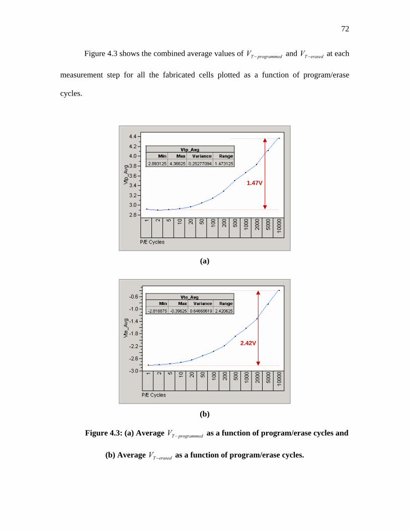
72
Figure 4.3 shows the combined average values of and at each
measurement step for all the fabricated cells plotted as a function of program/erase
cycles.
programmedTV − erasedTV −
1.47V
(a)
2.42V
(b)
Figure 4.3: (a) Average as a function of program/erase cycles and
(b) Average as a function of program/erase cycles.
programmedTV −
erasedTV −

73
It can be seen from figure 4.3 that at the end of 10,000 program/erase cycles,
TV −
is considerably sharper (~165%) as com
of net positive charge (holes) in
the tun
programmed increased by 1.47V where as erasedTV − increased by 2.42V i.e. the rise in
d to programmedTV − .
As discussed before, there is an initial generation
erasedTV − pare
nel oxide, however, that phenomenon is short-lived. As a consequence of positive
charge generation in the tunnel oxide, which enhances the tunneling efficiency, an initial
slight decrease in erasedTV − may sometimes be observed [8,25,28]. The phenomenon of
slight initial decrea erased− was observed in a few of the fabricated cells, as shown
in figure 4.4.
se in TV
Figure 4.4: Variability chart showing a slight initial decrease in erasedTV − .

74
4.1.2 ENDURANCE CHARACTERIZATION USING PROGRAM/ERASE VERIFY SCHEMES
n
be com
ase in and an increase in is typically seen with
program gram
As discussed earlier, the threshold voltage shift and memory window closure ca
pensated by means of program and erase verify schemes. The cell threshold
voltage is checked after a program or erase operation in order to determine whether or not
the target TV has been achieved and, if not, programming or erasing is continued until the
cell is verified to have been programmed or erased. In NAND Flash memory cells, as
shown before, programmedTV − increases with P/E cycling when fixed programming
conditions are used (no program verify scheme). That means that with increasing
program/erase cycle, the cells require less than standard/initial programming to raise the
threshold voltage to the required programmedTV − (since standard programming conditions are
raising the threshold voltage to a value higher than that is required). That translates to a
decrease in programt as the number of P/E cycles increases when a program verify scheme
is used. On the other hand, the increase in erasedTV − with P/E cycling (when no erase verify
scheme is used) means that more than st erase conditions (i.e. number of erase
pulses/pulse widths/pulse heights) are now required to lower the threshold voltage of the
cell to an acceptable level of erasedTV − . That translates to an increase in eraset as the number
of P/E cycles increases.
Overall, a decre
andard
programt eraset
/erase cycling when pro /erase verify schemes are used. That is why the
typical failure mechanism in conventional NAND Flash memory cells is erase verify
failures i.e. eraset rises to a value larger than the device specification limit.

75
Endurance cycling, using program/erase verify schemes, was performed on MLC
NAND Flash memory cells fabricated on different silicon wafers (each silicon wafer
contains over 350 fabricated chips with a capacity of 16Gb on each chip) for repeatability
verification. Figure 4.5 shows variability charts for the number of required program and
erase pulses (which directly translates to and ) as a function of program/erase
cycles.
programt eraset

76
(a)
(b)
Figure 4.5: Variability chart for (a) the number of erase pulses needed as a
function of the number of cycles and (b) the number of program pulses needed as a
function of the number of cycles.
77
As expected, a sharp increase in the number of required erase pulses was seen
with extended cycling. At the same time, a slight decrease in the number of required
program pulses (which translates directly to decrease in ) was observed. It is
obvious from figure 4.5 that the primary failure mechanism in the fabricated NAND
Flash memory cells was erase verify failures. During the program operation, the increase
in intrinsic threshold voltage actually helps to raise the threshold voltage of the cell i.e.
decreases. Therefore program verify failures are not a concern at this point.
programt
programt
In summary, the increase in intrinsic threshold voltage due to electron trapping in
the tunnel oxide is the primary failure mechanism and therefore a major issue as far as the
reliability and endurance of NAND Flash memory cells are concerned.
It can be noted from figure 4.5 that the average number of program pulses needed
for fresh cells is much higher compared to the number of erase pulses needed. That is due
to the fact that programming pulses are applied in small increments to avoid over-
programming the cell and also to avoid inadvertently programming neighboring cells
(‘Program Disturb’ mechanism). The key to successful programming is to move the
threshold voltage up as gently as possible (yet hard enough to minimize the time to
program). On the other hand, since the erase operation is done one block at a time, a high
enough voltage pulse can be applied to erase the cells in the shortest amount of
time/pulses.

78
4.2 A NOVEL METHOD FOR ENDURANCE IMPROVEMENT:
In this work, a novel NAND Flash memory cell design has been proposed which
eliminates tunnel oxide degradation caused by Fowler-Nordheim tunneling and therefore
improves the long-term reliability and endurance of NAND Flash memory cells. Device
simulations and analysis have been provided demonstrating how the proposed cell design
provides superior endurance and reliability as compared to the conventional Flash
memory cells.
In a conventional NAND Flash memory cell, the tunnel oxide is used to tunnel
electrons to and from the floating gate and that, in turn, degrades the oxide. The cross-
section view of a conventional NAND Flash memory cell and schematic view of a
conventional NAND Flash memory array structure are shown in figures 2.4 and 2.8,
respectively.
The proposed cell design, namely ‘NAND Flash Memory Cell with Pseudo
Wordline’ is shown in figure 4.6.
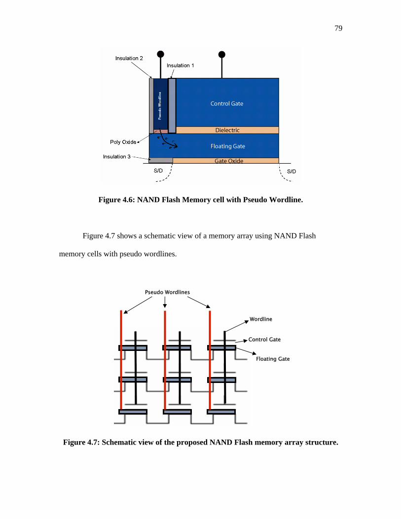
79
Figure 4.6: NAND Flash Memory cell with Pseudo Wordline.
Figure 4.7 shows a schematic view of a memory array using NAND Flash
memory cells with pseudo wordlines.
Wordline
Floating Gate
Control Gate
Pseudo Wordlines
Figure 4.7: Schematic view of the proposed NAND Flash memory array structure.

80
As can been seen from figures 4.6 and 4.7, the proposed cell design has an
external polysilicon line running parallel to the wordline which is used to tunnel electrons
to and from the floating gate and connected directly to the floating gate through a layer of
polyoxide.
During the erase operation, electrons are tunneled from the floating gate through
the tunnel oxide in a conventional NAND Flash memory cell. However, in the proposed
NAND Flash memory cell, electrons are tunneled out of the floating gate via the
polyoxide. In other words, the proposed NAND Flash memory cell uses the polyoxide to
tunnel electrons to and from the floating gate during both the program and erase
operations, as opposed to a conventional NAND Flash memory cell which uses the gate
oxide where has for the tunneling processes.
The only major differences between a conventional NAND Flash memory cell
and the proposed NAND Flash memory cell are that:
• The cell is programmed by applying to the control gate and grounding the
pseudo wordline instead of the substrate/p-well.
programV
• The cell is erased by grounding the control gate and applying to the pseudo
wordline instead of the substrate/p-well.
eraseV

81
Table 4.1: Comparison of operation conditions between the conventional and
proposed NAND Flash memory cell.
RReeaadd PPrrooggrraamm EErraassee
CCoonnvveennttiioonnaall cceellll readV applied to
Control Gate and substrate/p-well
grounded
programV applied to Control Gate and substrate/p-well
grounded
eraseV applied to substrate/p-well and
Control Gate grounded
PPrrooppoosseedd cceellll readV applied to
Control Gate and substrate/p-well
grounded
programV applied to Control Gate and pseudo wordline
grounded
eraseV applied to pseudo wordline and
Control Gate grounded
As explained above, the external poly line in the proposed NAND Flash memory
cell is used for program and erase only. The proposed cell is read through the control gate
just like in a conventional cell, however, during the program/erase operations, electrons
are tunneled to and from the control gate via the pseudo wordline, instead of the
substrate.
The primary advantage of the proposed cell design is that it will eliminate any
high field/current stressing of the tunnel oxide and hence eliminate any degradation of the
tunnel oxide. That will directly translate into an increase in the reliability and endurance
of the NAND Flash memory cell.

82
4.2.1 SIMULATION SOFTWARE - BACKGROUND INFORMATION
In this work, the Sentaurus TCAD tool suite by Synopsis®, Inc. was used for
device simulations. Technology Computer-Aided Design (TCAD) refers to the use of
computer simulations to develop and optimize semiconductor processing technologies
and devices. Synopsys TCAD offers a comprehensive suite of products that includes
industry leading process and device simulation tools, as well as a powerful GUI-driven
simulation environment for managing simulation tasks and analyzing simulation results
[35].
The structure of a device is approximated by a mesh (1D, 2D, or 3D) consisting of
a large number of discrete elements. Differential equations describing the electric
potential and carrier distributions are applied to each element. Boundary conditions for
the simulation are chosen e.g. potentials at each electrode. The equations to find the
potential and carrier concentrations in each element are then solved. The software uses a
numerical solver using an iterative process where the iterations are user defined.
Overall, the simulation process can be broken into three main parts: building the
device structure, running the simulation, and viewing the results.
Building the Device Structure (using Sentaurus Structure Editor):
The Sentaurus Structure Editor tool is used to create the device structure. It is a
device editor and process emulator based on CAD technology [36]. It can be used for 2D
or 3D structure editing and 3D process emulation to create TCAD devices. In Sentaurus
Structure Editor, structures are generated or edited interactively using the graphical user
interface (GUI). From the GUI, 2D and 3D device models are created geometrically

83
using 2D or 3D primary shapes such as rectangles, polygons, cuboids, cylinders, and
spheres. 3D regions can also be created by simple extrusion of 2D objects or by sweeping
2D objects along a path. Doping profiles and meshing strategies can also be defined
interactively. Sentaurus Structure Editor features an interface to configure and call the
Synopsys meshing engines. In addition, it generates the necessary input files for the
meshing engines, which generate the grid and data files for the device structure.
The mesh takes boundary (.bnd) and command (.cmd) files as arguments. The
‘StripDetector.bnd’ boundary file describes materials and contacts and the
‘StripDetector.cmd’ describes doping profiles and mesh refinement.
Running the Simulation (using Sentaurus Device):
Sentaurus Device is an advanced multidimensional device simulator capable of
simulating electrical, thermal, and optical characteristics of silicon-based and compound
semiconductor devices [37]. It is a new-generation device simulator for designing and
optimizing current and future semiconductor technologies such as nanoscale CMOS,
FinFET, thin film transistors (TFTs), SiGe heterojunction bipolar transistors (HBTs),
large-scale power devices, compound semiconductors, CMOS image sensors, light-
emitting diodes, semiconductor lasers, and Flash memory. Advanced physics and the
ability to add user-defined models in Sentaurus Device allow for investigation of novel
structures made from new material. Sentaurus Device is capable of simulating the
electrical, thermal, and optical characteristics of silicon and compound semiconductor
devices.
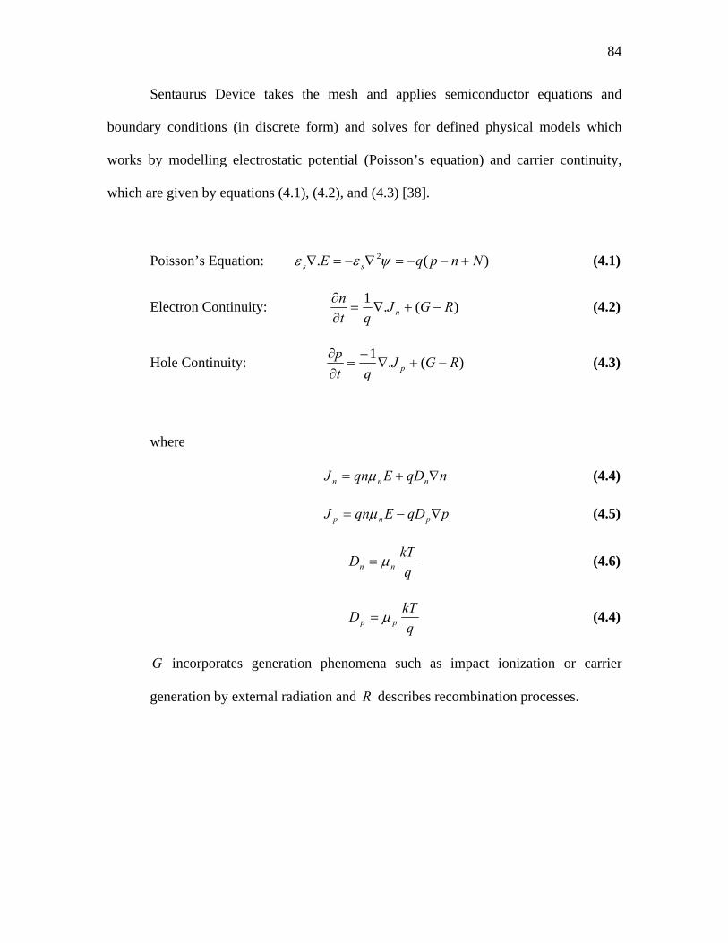
84
Sentaurus Device takes the mesh and applies semiconductor equations and
boundary conditions (in discrete form) and solves for defined physical models which
works by modelling electrostatic potential (Poisson’s equation) and carrier continuity,
which are given by equations (4.1), (4.2), and (4.3) [38].
Poisson’s Equation: (4.1) )(. 2 NnpqE ss +−−=∇−=∇ ψεε
Electron Continuity: )(.1 RGJqt
nn −+∇=
∂∂ (4.2)
Hole Continuity: )(.1 RGJqt
pp −+∇
−=
∂∂ (4.3)
where
nqDEqnJ nnn ∇+= μ (4.4)
pqDEqnJ pnp ∇−= μ (4.5)
q
kTD nn μ= (4.6)
q
kTD pp μ= (4.4)
G incorporates generation phenomena such as impact ionization or carrier
generation by external radiation and R describes recombination processes.

85
The Sentaurus Device command file (*_des.cmd) specifies the following:
File - Input and output files
Electrode - List of the device contacts
Physics - Physics models used in simulation
Plot and CurrentPlot - Variables in included in output files
Math - Controls for solver
Solve - Simulation conditions
Sentaurus Device has various physics models available to simulate semiconductor
devices. The basic physics models include mobility, generation-recombination, and
effective intrinsic density. Material-dependent parameters and interface and contact
boundary conditions can also be defined in the Physics section of the syntax.
Mobility Model: Carrier scattering by impurity ions in doped semiconductors leads to
carrier mobility degradation. The model for mobility degradation due to impurity
scattering is activated by specifying the ‘DopingDep’ term in the Mobility section of the
syntax within the Physics section. In the presence of high electric fields, the carrier drift
velocity is no longer proportional to the field, and can thus no longer be described by a
field-independent mobility. Instead, the velocity saturates to a finite value. The high-field
carrier velocity saturation models are composed of three submodels: the actual mobility
model, the velocity saturation model, and the driving force model.

86
Recombination Model: Sentaurus Device has different parameters available to define the
generation-recombination model. The basic Shockley-Read-Hall model for
recombination and generation of electron-hole pairs (generation and recombination due to
traps distributed in the forbidden band with doping dependence) is used by specifying the
’SRH (DopingDep)’ term in the Recombination section of the syntax within the Physics
section. The effects of band-to-band (BB) tunneling are included by using the
Band2Band model. The band-to-band tunneling model describes the generation of
carriers in high field regions without any influence of local traps. The band-to-band
tunneling process describes the field emission of valence electrons leaving back holes.
Another physics model that is available in Sentaurus Device is the Avalanche model. It
simulates the increase in generation from impact ionization.
Band Gap Model: The bandgap model is selected by using the ‘EffectiveIntrinsicDensity’
statement in the Physics section. This models narrowing of the bandgap at high doping
concentrations and high temperatures.

87
The physics model used for device simulations in this work is given by the
following syntax:
Physics { Temperature=300 eQCvanDort EffectiveIntrinsicDensity(OldSlotboom) Mobility( DopingDep HighFieldsaturation(GradQuasiFermi) Enormal ) Recombination( Band2Band SRH( DopingDep ) Avalanche(Eparallel) ) }
Another useful model available in Sentaurus Device is the Oxide Charge model.
Physics models can be specified for particular device regions by inserting a separate
Physics section. Details of physics models available in Sentaurus device can be found in
the software user guide [39].
The Solve section of the syntax allows various processes such as solution of
Poisson’s equation which simply solves the device under steady state bias conditions.
The Quasistationary function ramps a parameter (such as bias voltage) from an initial
value to a final value in a series of steps and the device is solved for a steady state at each
point e.g. simulating the IV response of a transistor . The Transient function allows
simulation over time. The stepping conditions in each case are user defined. Sentaurus
Device solves each step by an iterative process and the limit to the number of iterations
is, again, user defined.

88
Viewing the Results:
The Inspect function can be used to create graphs (from *.plt files created by
Sentaurus Device). Any pair of data sets such as electrode voltages, currents, etc. can be
plotted.

89
An example of a 3D mesh structure and associated doping distribution is shown in
figure 4.8 [36].
Figure 4.8: Visualization of a 3D mesh structure and associated doping
distribution.

90
An example showing the doping profile of a 3D PMOS transistor with SiGe
source/drain pockets is shown in figure 4.9 [37].
Figure 4.9: Doping profile of a 3D PMOS transistor with SiGe source/drain pockets.

91
4.2.2 DEVICE SIMULATIONS
A conventional NAND Flash memory cell and the proposed cell were simulated
(using the Sentaurus TCAD tool suite by Synopsys®, Inc.). The physics models used have
been discussed earlier in this chapter. The 3D cell structures built for simulations of the
two devices are shown in figure 4.10.
Figure 4.10: Conventional NAND Flash memory cell (left) as compared to the
proposed Flash memory cell (right).
It must be noted that the oxide layers in the conventional NAND Flash memory
cell structure shown in figure 4.9 have been displayed as non-visible. That has been done
for a better 3D representation of the cell, including the IPD and control gate wrapping
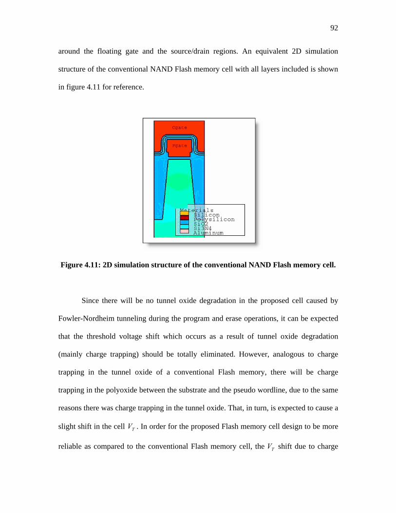
92
around the floating gate and the source/drain regions. An equivalent 2D simulation
structure of the conventional NAND Flash memory cell with all layers included is shown
in figure 4.11 for reference.
Figure 4.11: 2D simulation structure of the conventional NAND Flash memory cell.
Since there will be no tunnel oxide degradation in the proposed cell caused by
Fowler-Nordheim tunneling during the program and erase operations, it can be expected
that the threshold voltage shift which occurs as a result of tunnel oxide degradation
(mainly charge trapping) should be totally eliminated. However, analogous to charge
trapping in the tunnel oxide of a conventional Flash memory, there will be charge
trapping in the polyoxide between the substrate and the pseudo wordline, due to the same
reasons there was charge trapping in the tunnel oxide. That, in turn, is expected to cause a
slight shift in the cell . In order for the proposed Flash memory cell design to be more
reliable as compared to the conventional Flash memory cell, the shift due to charge
TV
TV
93
trapping in the polyoxide under the pseudo wordline must be smaller as compared to the
shift due to charge trapping in the tunnel oxide of a conventional Flash memory cell. TV
Figure 4.12 shows the shift in the I-V curve of the proposed Flash memory cell,
using different dielectric constants for IPD, for a constant trapped charge
(Qf = in this case) in the polyoxide as compared to a shift in the IV
curve of the conventional Flash memory cell for various values of constant trapped
charge in the tunnel oxide (Q
212 /105 cmC×−
f = , , ). 212 /105 cmC×− 212 /102 cmC×− 212 /101 cmC×−

94
(a)
(b)
Figure 4.12: Shift in the I-V curve of (a) the proposed memory cell and (b) the
conventional memory cell caused by charge trapping.

95
It can be seen from figure 4.8 that the shift in due to a trapped charge of
Q
TV
f = at the polyoxide interface (in the proposed cell) is less than 0.5V as
compared to the ‘failure to turn on’ caused by the same amount of trapped charge in the
tunnel oxide-Si interface (in the conventional cell). A failure to turn on occurs when the
cell threshold voltage exceeds the maximum allowed value (3V in this case) i.e. the cell
threshold voltage cell has reached the device specification limit.
212 /105 cmC×−
Furthermore, it can be seen that the effect on cell threshold voltage of trapped
charge (Qf = ) at the at the tunnel oxide-Si interface in the conventional
cell is twice as compared to the effect on cell threshold voltage of a five times higher
trapped charge (Q
212 /101 cmC×−
f = ) at the polyoxide interface in the proposed cell. 212 /105 cmC×−
In summary, the shift caused by charge trapping in the proposed NAND Flash
memory cell is approximately 1000% less compared to the shift seen in the
conventional cell. That, according to the measured endurance characteristics of cells
fabricated in this work (presented later in this chapter), translates to an increase of over
two orders of magnitude in program/erase endurance. It can be deduced that, as compared
to conventional cells, the proposed cell design is 10 times more immune to charge
trapping and offers an over 200 times improvement in program/erase endurance. The
simulations results discussed above have been summarized in table 4.2.
TV
TV
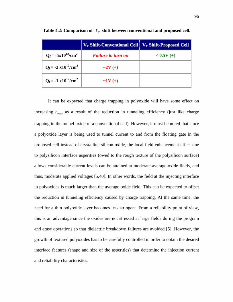
96
Table 4.2: Comparison of shift between conventional and proposed cell. TV
VVTT SShhiifftt--CCoonnvveennttiioonnaall CCeellll VVTT SShhiifftt--PPrrooppoosseedd CCeellll
Qf = -5x10¹²/cm2 Failure to turn on < 0.5V (+)
Qf = -2 x10¹²/cm2 ~2V (+)
Qf = -1 x10¹²/cm2 ~1V (+)
It can be expected that charge trapping in polyoxide will have some effect on
increasing as a result of the reduction in tunneling efficiency (just like charge
trapping in the tunnel oxide of a conventional cell). However, it must be noted that since
a polyoxide layer is being used to tunnel current to and from the floating gate in the
proposed cell instead of crystalline silicon oxide, the local field enhancement effect due
to polysilicon interface asperities (owed to the rough texture of the polysilicon surface)
allows considerable current levels can be attained at moderate average oxide fields, and
thus, moderate applied voltages [5,40]. In other words, the field at the injecting interface
in polyoxides is much larger than the average oxide field. This can be expected to offset
the reduction in tunneling efficiency caused by charge trapping. At the same time, the
need for a thin polyoxide layer becomes less stringent. From a reliability point of view,
this is an advantage since the oxides are not stressed at large fields during the program
and erase operations so that dielectric breakdown failures are avoided [5]. However, the
growth of textured polyoxides has to be carefully controlled in order to obtain the desired
interface features (shape and size of the asperities) that determine the injection current
and reliability characteristics.
eraset

97
4.2.3 DESIGN CHALLENGES
Due to the reduced area of contact between the floating gate and the control gate
in the proposed NAND Flash memory cell as compared to the conventional cell, a
reduction in the gate coupling ratio (GCR) is expected.
Gate coupling ratio is the fraction of the applied voltage that is ‘seen’ by the
floating gate. Mathematically, gate coupling ratio is total
erpoly
CCint where is the
capacitance of the dielectric between the control gate and the floating gate (IPD) and
is the sum of all parasitic capacitances (discussed in detail in chapter 2) of the Flash
memory cell. Several techniques have been presented to extract the gate coupling ratios
from simple dc measurements. The most commonly used methods are 1) linear threshold
voltage technique, 2) subthreshold slope method, and 3) transconductance technique [12].
These techniques require the measurement of the electrical parameters in a memory cell
and in a “dummy” cell i.e. a device identical to the memory cell, but with floating and
control gates connected to each other. By comparing the results, the gate coupling
coefficient can be determined. Other methods have been proposed to extract the gate
coupling coefficients directly from the memory cell without using a “dummy” cell [41].
erpolyCint
totalC
However, it must be noted that a polyoxide layer is being used to tunnel current to
and from the floating gate in the proposed cell instead of crystalline silicon oxide. The
local field enhancement effect due to polysilicon interface asperities (owed to the rough
texture of the polysilicon surface) allows considerable current levels can be attained at
moderate average oxide fields, and thus, moderate applied voltages [5,40]. In other
words, the field at the injecting interface in polyoxides is much larger than the average
oxide field. That means that the required injection efficiency can be achieved in the
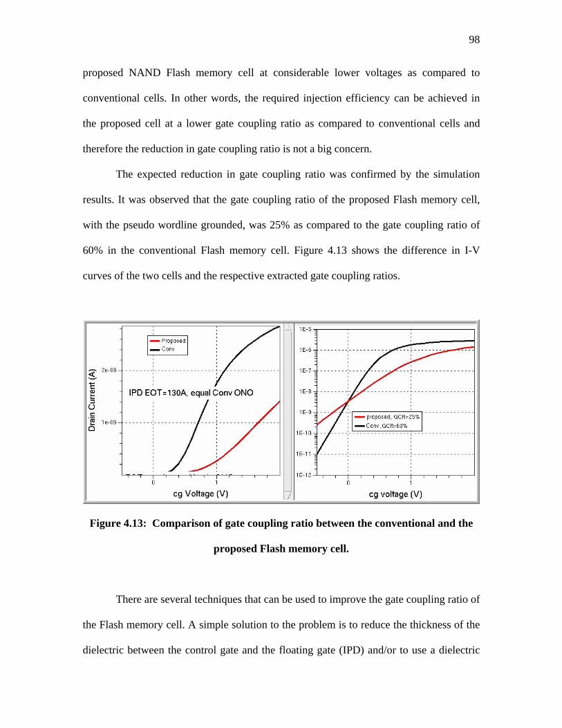
98
proposed NAND Flash memory cell at considerable lower voltages as compared to
conventional cells. In other words, the required injection efficiency can be achieved in
the proposed cell at a lower gate coupling ratio as compared to conventional cells and
therefore the reduction in gate coupling ratio is not a big concern.
The expected reduction in gate coupling ratio was confirmed by the simulation
results. It was observed that the gate coupling ratio of the proposed Flash memory cell,
with the pseudo wordline grounded, was 25% as compared to the gate coupling ratio of
60% in the conventional Flash memory cell. Figure 4.13 shows the difference in I-V
curves of the two cells and the respective extracted gate coupling ratios.
Figure 4.13: Comparison of gate coupling ratio between the conventional and the
proposed Flash memory cell.
There are several techniques that can be used to improve the gate coupling ratio of
the Flash memory cell. A simple solution to the problem is to reduce the thickness of the
dielectric between the control gate and the floating gate (IPD) and/or to use a dielectric

99
material with a higher dielectric constant ( κ ). It has been demonstrated in a study
conducted by Mansouri et al. [42] that the gate coupling ratio of a floating gate cell is
significantly improved when the EOT (equivalent oxide thickness) of the IPD is reduced,
as shown in figure 4.14.
1.E-05
1.E-04
EOT=3.5nm
EOT=5.0nm
EOT=85nm
EOT=9.0nm
EOT=13.5nm
EOT=00%
20%
40%
60%
80%
100%( D ) ( E ) ( C ) ( B ) ( A) Reference
GC
R (g
ate
coup
ling
ratio
)
Figure 4.14: Gate coupling ratio as a function of IPD EOT.
The proposed NAND Flash memory cell was simulated for IPDs with different of
κ values to verify the expected increase in GCR when the dielectric constant is increased
and/or the EOT is reduced. Using an IPD with a dielectric constant of 20 (EOT=33 )
resulted in a gate coupling ratio of 46% (as compared to a gate coupling ratio of 60% in
the conventional cell). Using an IPD with a dielectric constant of 35 (EOT=19 )
resulted in a gate coupling ratio of 57%. Figure 4.15 shows the IV curves and respective
oA
oA

100
calculated gate coupling ratios of the above mentioned combinations of IPD thicknesses
and dielectric constants.
Figure 4.15: IV curves and respective GCRs using various IPD thicknesses and
dielectric constants.
In order to further improve the gate coupling ratio without the need of an IPD
layer with a κ value as high as 35, a technique that can be used is to float the pseudo
wordline during the read operation. It was observed that floating the pseudo wordline
during the read operation improved the gate coupling ratio substantially. Using an IPD
with a dielectric constant of 5.1 (EOT=130 , which is the oA κ /EOT of the IPD used in the
conventional cell) resulted in a gate coupling ratio of 43%. Using an IPD with a dielectric
constant of 20 (EOT=33 ) resulted in a gate coupling ratio of 59%, which is comparable oA
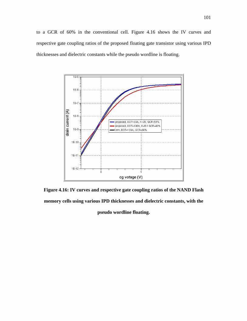
101
to a GCR of 60% in the conventional cell. Figure 4.16 shows the IV curves and
respective gate coupling ratios of the proposed floating gate transistor using various IPD
thicknesses and dielectric constants while the pseudo wordline is floating.
Figure 4.16: IV curves and respective gate coupling ratios of the NAND Flash
memory cells using various IPD thicknesses and dielectric constants, with the
pseudo wordline floating.

102
Overall, it was shown that reasonable gate coupling can be achieved in the
proposed cell. Also, since the need of a very high gate coupling ratio in the proposed cell
(due to local field enhancement effect of the polyoxide) is not as stringent as compared to
conventional cells, the issue of reduction in gate coupling ratio is not a big concern
during the program and erase operations.
A summary of the GCRs achieved using IPD films with various dielectric
constants is shown in table 4.3.
Table 4.3: GCRs achieved using IPD films with various dielectric constants.
IIPPDD κκ VVaalluuee EEOOTT ((Å)) GGCCRR ((%%))
CCoonnvveennttiioonnaall CCeellll 5.1 130 60
20 33 46 Proposed Cell (Pseudo WL Grounded) 35 19 57
5.1 130 43 Proposed Cell (Pseudo WL Floating) 20 33 59
The IPD film used in the conventional device is ONO (κ =5.1 and breakdown
electric field ~7x10⁶ V/cm). In order to achieve higher κ values such as 20, either
(252 TiOOTa − κ =20 and breakdown electric field ~7x10⁶ V/cm) or various
combinations of different high-κ dielectric materials such as , , and
can be used. The properties of compound dielectric materials (
2HfO 32OAl 2ZrO
κ value, band gap energy,
etc.) are determined by the relative concentrations of the different dielectric materials in
the compound.

103
High-dielectric-constant materials such as , , and have been
extensively studied by researchers. exhibits a large band gap (~8.9eV), a large
conduction band offset of 2.8eV with respect to silicon, a dielectric constant (
2HfO 32OAl 2ZrO
32OAl
κ ) of 9-12,
high filed strength, and excellent thermal stability. On the other hand, exhibits a
high dielectric constant (
2HfO
κ ) of 25-30, a relatively smaller band gap of ~5.68eV, and
relatively low thermal stability (due to crystallization at high temperatures leading to
current leakage and breakdown) [43,44]. To take advantage of the large energy band gap
and thermal stability of and the high dielectric constant of , a compound of
the two materials i.e. hafnium-aluminum-oxide ( ) can be used.
32OAl 2HfO
xx OAlHfO −1322 )()(
It has been shown that the κ value, band gap energy, and hence, band offsets with
respect to silicon is proportional the relative concentrations of and [45].
The dielectric constant and crystallinity of hafnium-aluminum-oxide can be controlled by
varying the relative concentrations of and [43]. The relative concentrations
of and can be adjusted by varying the number of deposition cycles in the
atomic layer deposition (ALD) system. Overall, the hafnium-aluminum-oxide films show
higher
2HfO 32OAl
2HfO 32OAl
2HfO 32OAl
κ values as compared to films and significantly improved leakage currents
and breakdown voltages as compared to films [43]. Hafnium-aluminum-oxide
films with 90% (and 10% ) have shown a
32OAl
2HfO
2HfO 32OAl κ value of 19 [46]. At the same
time, zirconium-aluminum-oxide has been shown to have a κ value between 11.84 and
20.96 [47].

104
Studies have been conducted showing that it is feasible to replace the
conventional IPD stack (ONO) in Flash memory cells by high-k materials such as
and in order to significantly improve the gate coupling ratio of the
floating gate cell [42]. It was also observed in [42] that, as compared to ONO,
and had lower leakage current as a function of temperature, as shown in
figure 4.17.
xHfAlO xZrAlO
xHfAlO xZrAlO
1.E-11
1.E-10
1.E-09
1.E-08
1.E-07
-25 25 75 125 175 225
Temperature (˚C)
Cur
rent
(A)
ZrAlOONO
HfAlO
SiO2 Z2
rO
x
x
Figure 4.17: Temperature dependence of leakage current.

105
Table 4.4 shows the relative dielectric constants ( rε ) and corresponding
breakdown electrics fields ( ) of several typical dielectric materials [48]. BDE
Table 4.4: Relative dielectric constants and corresponding breakdown electric fields
of several typical dielectric materials.

106
Another technique that can be used for improving the gate coupling ratio is to
wrap the CG around the open side of the FG. This will significantly increase the surface
area of contact and improve the gate coupling ratio. It must be noted that the conventional
NAND Flash memory cell uses the wrap-around technique for GCR improvement as
shown in figure 4.10. At the same time, recessing the control gate (CG) into the floating
gate (FG) will increase the surface area of contact between the CG and the FG and, in
turn, improve the gate coupling ratio.
In summary, the usage of high-k dielectrics such as and as
interpoly dielectric in combination with recessing the control gate into the floating gate
and wrapping the control gate around the open side of the floating gate will provide a
reasonably high GCR ratio. It is possible that recessing the CG into the FG and wrapping
the CG around the open side of the FG may result in a sufficient GCR so that replacing
the existing interpoly dielectric with a high-k material might not be necessary.
xHfAlO xZrAlO
4.2.4 POTENTIAL CONCERNS AND CORRESPONDING SOLUTIONS
A couple of potential concerns that might affect the performance of the proposed
NAND Flash memory cell are current crowding at the corner of the pseudo wordline and
reduced tunneling efficiency due to the smaller surface area of the polyoxide (as
compared to the surface area of the tunnel oxide in a conventional cell).
As can be seen in figure 4.18, in the originally proposed cell design, there is a
sharp corner at the edge of the pseudo wordline and the floating gate. This sharp corner
can potentially cause current crowding during the program and erase operations.

107
Figure 4.18: The originally proposed NAND Flash memory cell has a sharp corner
between the pseudo wordline and the floating gate.
The surface area of contact between the pseudo wordline and the floating gate in
the proposed cell is smaller as compared to the surface area of contact between the
control gate and the floating gate in the conventional cell. This reduction in the surface
area of contact can be expected to cause some reduction in Fowler-Nordheim tunneling
efficiency during the program and erase operations.
The solution for the above mentioned concerns is to have a rounded edge between
the pseudo wordline and the floating gate and to increase the surface area of contact
between the pseudo wordline and the floating gate.
Rounding of the edge and increase in the surface area of contact are both achieved
by recessing the pseudo wordline into the floating gate as shown in figure 4.19.

108
Figure 4.19: Pseudo wordline recessed into the floating gate in order to avoid
current crowding and improve tunneling efficiency.
As discussed before, a polyoxide layer is being used to tunnel current to and from
the floating gate in the proposed cell instead of crystalline silicon oxide. The local field
enhancement effect due to polysilicon interface asperities (owed to the rough texture of
the polysilicon surface) allows considerable current levels can be attained at moderate
average oxide fields, and thus, moderate applied voltages [5,40]. In other words, the field
at the injecting interface in polyoxides is much larger than the average oxide field. This,
in combination with an increased surface area of contact, is expected to further offset any
reduction in tunneling current density caused by the reduced area of contact. At the same
time, the need for a thin polyoxide layer becomes less stringent. From a reliability point
of view, this is an advantage since the oxides are not stressed at large fields during the
program and erase operations so that dielectric breakdown failures are avoided [5].
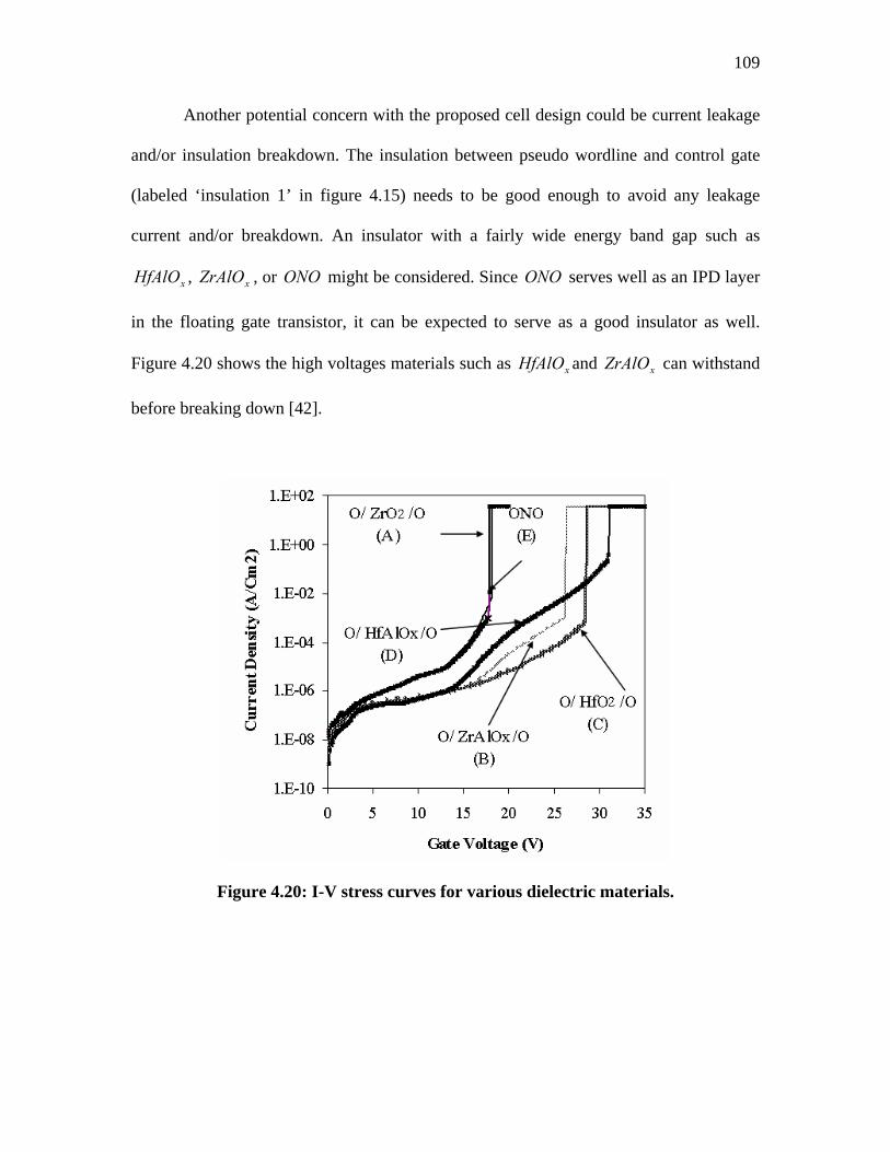
109
Another potential concern with the proposed cell design could be current leakage
and/or insulation breakdown. The insulation between pseudo wordline and control gate
(labeled ‘insulation 1’ in figure 4.15) needs to be good enough to avoid any leakage
current and/or breakdown. An insulator with a fairly wide energy band gap such as
, , or ONO might be considered. Since serves well as an IPD layer
in the floating gate transistor, it can be expected to serve as a good insulator as well.
Figure 4.20 shows the high voltages materials such as and can withstand
before breaking down [42].
xHfAlO xZrAlO ONO
xHfAlO xZrAlO
Figure 4.20: I-V stress curves for various dielectric materials.

110
Summary:
In this chapter, endurance characterization and analysis of fabricated MLC
NAND Flash memory devices was presented which reconfirmed the issue of limited
program/erase endurance and reliability of NAND Flash memory devices. A novel
NAND Flash memory cell design was proposed which eliminates tunnel oxide
degradation caused by Fowler-Nordheim tunneling and therefore improves the long-term
reliability and endurance of the NAND Flash memory cell. The structure and function of
the proposed cell were compared to conventional NAND Flash memory cells and
discussed in detail. Basic background information of the device simulation software used
in this work was then discussed. Device simulation results for conventional and proposed
cell designs were presented and analyzed showing that the proposed cell design is
superior to conventional NAND Flash memory cells in terms of endurance and reliability.
It was shown that the proposed cell design offers a more than 1000% reduction in
intrinsic threshold voltage shift caused by charge trapping which, according to the
measured endurance characteristics of cells fabricated in this work, translates to an
improvement of over two orders of magnitude in program/erase endurance. Some design
challenges and corresponding solutions were then discussed in this chapter. Finally, a
discussion about modifications that can be made to further improve the performance of
the proposed cell design was included in this chapter.

111
CHAPTER 5: CONCLUSIONS AND SUGGESTIONS FOR FUTURE WORK
Conclusions
Low power consumption, virtually zero latency, extremely fast boot-up for OS
and applications, fast data access, small size, light weight, and high shock resistance are
some of many reasons for the rapidly increasing popularity and demand for Flash
memory as a high density, non-volatile memory storage solution for a variety of portable
electronics such as wireless phones, personal digital assistants (PDAs), portable music
players, keychain USB drives, digital cameras, and many other applications. Among the
two types of Flash memory i.e. NAND and NOR Flash, NAND Flash is the ideal choice
for a vast variety of popular consumer electronics due to its the fast program/erase times,
lower cost per bit, and small size as compared to NOR Flash.
However, long-term reliability and endurance is a major concern and a limiting
factor when it comes to the adaptation of NAND Flash as an alternative for cheap and
efficient memory. Tunnel oxide degradation caused by high field/current stress during
Fowler-Nordheim tunneling is the governing phenomenon that causes reliability and
endurance issues in NAND Flash memory cells.
In this work, endurance characterization of fabricated NAND Flash memory cells
and a detailed analysis has been conducted which reconfirmed the issue of limited
program/erase endurance and reliability of NAND Flash memory devices. Subsequently,
a novel cell design has been proposed which eliminates tunnel oxide degradation caused
by Fowler-Nordheim tunneling. The proposed cell design, as compared to conventional
cells, offers a significant improvement to the long-term reliability and endurance of

112
NAND Flash memory cells. It has shown over 10 times more immunity to intrinsic
threshold voltage shift caused by charge trapping which translates to a greater than 200
times improvement in program/erase endurance, according to the measured endurance
characteristics of cells fabricated in this work.
Suggestions for future work
Although the reliability and endurance of NAND Flash memory cells has been an
area of interest for many researchers, there are still innumerable questions and concerns
yet to be addressed. Shortfalls in the current technology and design of NAND Flash
memory cells are issues warranting further research and development in this area. A few
recommendations for future research and development based on the present work are:
1. Additional simulations of the proposed cell with various combinations of suggested
improvements (wrapping the control gate around the open side of the floating gate,
recessing the control gate into the floating gate, recessing the pseudo wordline into the
floating gate, etc.) to find an optimum cell design.
2. Fabrication and testing of the proposed cell.
3. Detailed electrical characterization of the fabricated cell.
4. Study of various high κ dielectrics and their feasibility for use as IPD films in Flash
memory devices.
5. Additional research work to better understand charge trapping in thin oxides and its
effects on the reliability and endurance of floating gate semiconductor memory
devices.

113
REFERENCES
1. C. Clementi and R. Bez, “Non-Volatile Memory Technology: Floating Gate Cell
Concept Evolution”, Proceedings of Materials Research Society Symposium 830, 13 (2005)
2. Jim Cooke, “Flash Memory Technology Direction”, Microsoft WinHEC 2007,
http://download.micron.com/pdf/presentations/events/WinHEC_Cooke.pdf 3. Micron Technical Note, “NAND Flash 101: An Introduction to NAND Flash and
How to Design It In to Your Next Product, http://download.micron.com/pdf/technotes/nand/tn2919.pdf
4. A. R. Olson and D. J. Langlois, “Solid State Drives Data Reliability and Lifetime”,
April 7, 2008, Imation Corp. whitepaper, http://www.imation.com/products/pdfs/SSD-Reliability-Lifetime-White-Paper.pdf
5. W. D. Brown and J. Brewer, “Nonvolatile Semiconductor Memory Technology: A
Comprehensive Guide to Understanding and Using NVSM Devices”, IEEE Press Series on Microelectronic Systems, Wiley-IEEE Press, NJ.
6. D. Ielmini, A. S. Spinelli, and A.L. Lacaita, “Recent developments on Flash
memory reliability”, Microelectronic Engineering 80, 321 (2005). 7. Samsung NAND Flash memory,
www.dataio.com/pdf/NAND/Samsung/NANDtechnology.pdf 8. R. Bez, E. Camerlenghi, A. Modelli, and A. Visconti, “Introduction to Flash
Memory”, Proceedings of the IEEE 91 (4), 489 (2003). 9. Technical Training Document, Micron Technology, Inc. 10. G. Molas, D. Deleruyelle, B. De Salvo, G. Ghibaudo, M. GelyGely, L. Perniola, D.
Lafond, and S. Deleonibus, “Degradation of floating-gate memory reliability by few electron phenomena”, IEEE Transactions on Electron Devices 53, 2610 (2006).
11. P. Canet, V. Bouquet, F. Lalande, J. Devin, and B. Leconte, “Fowler-Nordheim
Erasing Time Prediction in Flash Memory”, Proceedings of the 6th Annual Non-Volatile Memory Technology Symposium, Dallas, Texas (2005).
12. P. Pavan, R. Bez, P. Olivo, and E. Zanoni, “Flash Memory Cells-An Overview”,
Proceedings of the IEEE 85 (8) (1997). 13. M. Lenzlinger and E. H. Snow, “Fowler-Nordheim Tunneling into Thermally
Grown SiO2”, Journal of Applied Physics 40 (1), 278 (1969).

114
14. J. G. Simmons, “Transition from Electrode-Limited to Bulk-Limited Conduction Processes in Metal-Insulator-Metal Systems”, Physical Review 166 (3), 912 (1968).
15. J. A. Lopez-Villanueva, J. A. Jimenez-Tejada, P. Cartujo, J. Bausells, and J. E.
Carceller, “Analysis of the effects of constant-current Fowler-Nordheim-tunneling injection with charge trapping inside the potential barrier”, Journal of Applied Physics 70, 7 (1991).
16. P. Olivo, J. Sune, and B. Ricco, “Determination of the Si-SiO2 Barrier Height from
the Fowler -Nordheim Plot”, IEEE Electronic Device Letters 12 (11) (1991). 17. M. Kamiya, Y. Kojima, Y. Kato, K. Tanaka, and Y. Hayashi, “EPROM Cell with
High Gate Injection Efficiency”, IEEE IEDM Tech. Dig., 741 (1981). 18. B. Euzent, N. Boruta, J. Lee, and C. Jenq, “Reliability Aspects of a Floating Gate
E2 PROM”, 19th Annual Reliability Physics Symposium, 11 (1981). 19. H. Jeong and K. Kim, “Prospect of Emerging Nonvolatile Memories”, Proceedings
of Materials Research Society Symposium 830, 363 (2005) 20. P. Cappelletti, R. Bez, D. Cantarelli, and L. Fratin, “Failure Mechanisms of Flash
Cell in Program/Erase Cycling”, IEEE IEDM Technical Digest 91, 294 (1994). 21. H. Fukuda, T. Hayashi, A. Uchiyama, and T. Iwabuchi, “Determination of Trapped
Oxide Charge in Flash-Type EEPROMs with Heavily Oxynitrided Tunnel Oxide Films”, Electronic Letters 29 (11), 947 (1993).
22. B. E. Deal, “Standardized Terminology for Oxide Charges Associated with
Thermally Oxidized Silicon”, IEEE Transactions on Electronic Devices 27 (3), 606 (1980).
23. C. S. Jena, T. R. Ranganath, C. H. Huang, H. S. Jones, and T. T. L. Chang, “High-
Field Generation of Electron Traps and Charge Trapping in Ultra-Thin SiO2”, IEEE IEDM 388 (1981).
24. J. Wu, E. Rosenbaum, B. MacDonald, E. Li, J. Tao, B. Tracy, and P. Fang, “Anode
Hole Injection versus Hydrogen Release: The Mechanism for Gate Oxide Breakdown”, 38th Annual IEEE International Proceedings on Reliability Physics, 27 (2000).
25. I. C. Chen, S. Holland, and C. Hu, “Hole Trapping and Breakdown in Thin SiO2”,
IEEE Electronic Device Letters EDL-7 (3), 164 (1986). 26. Y. Ohij and M. Ushiyama, “Thin Oxide on Si”, Journal of the Korean Physical
Society (Proc. Suppl.) 28, S1 (1995).

115
27. M. Liang and C. Hu, “Electron Trapping in Very Thin Thermal Silicon Dioxides”, IEEE IEDM, 396 (1981).
28. A. Modelli, A. Visconti, and R. Bez, “Advanced Flash Memory Reliability”, IEEE
International Conference on Integrated Circuit Design and Technology, 211 (2004). 29. K. T. San, C. Kaya, and T. P. Ma, “Effects of Erase Source Bias on Flash EPROM
Device Reliability”, IEEE Transactions on Electron Devices 42 (1), 150 (1995). 30. N. Mielke, A. Fazio, and H. Liou, “Reliability Comparison of FLOTOX and
Textured-Polysilicon E2PROMs”, 25th Proc. IRPS, 85 (1987). 31. H. Nozawa, N. Matsukawa, and S. Morita, “An EEPROM Cell Using a Low Barrier
Height Tunnel Oxide”, IEEE Transactions on Electron Devices ED-33 (2), 275 (1986).
32. K. Hieda, M. Wada, T. Shibata, I. Inoue, M. Momodomi, and H. Iizuka, “Optimum
Design of Dual Control Gate Cell for High Density EEPROM's”, IEEE IEDM Tech. Dig., 593 (1983).
33. Z. Liu, H. Wann, P. K. Ko, C. Hu, and Y. C. Cheng, “Improvement of Charge
Trapping Characteristics of N2O-Annealed and Reoxidized N2O-Annealed Thin Oxides”, IEEE Electron Device Letters 13 (10), 519 (1992).
34. J. Schmitz, “Flash Memories”,
http://www.el.utwente.nl/smi/content/education/is/stand_alone_flash_memories.ppt 35. Synopsis® TCAD,
http://www.synopsys.com/Tools/TCAD/Pages/default.aspx 36. Synopsis® Inc., Sentaurus Structure Editor Datasheet,
http://www.synopsys.com/Tools/TCAD/CapsuleModule/sde_ds.pdf 37. Synopsis® Inc., Sentaurus Device Datasheet,
http://www.synopsys.com/Tools/TCAD/CapsuleModule/sdevice_ds.pdf 38. W. Fichtner, D. J. Rose, and R.E. Bank, “Semiconductor Device Simulation”, IEEE
Transactions on Electron Devices 30 (9), 1018 (1983). 39. Synopsis® Inc., Sentaurus Device User Guide, Version Z-2007.03, Mountain View,
California, 2007. 40. M. Kimura, R. Nozawa, S. Inoue, and T. Shimoda, “Current Density Enhancement
at Active Layer Edges in Polycrystalline Silicon Thin-Film Transistors”, Japanese Journal of Applied Physics 40, L26 (2001).

116
41. Y. C. Park, “Flash Cell Erase Simulation, Characteristics and Validation through Coupling-Ratio Extraction”, Journal of the Korean Physical Society 45 (5), 1377 (2004).
42. S. Kar, R. Singh, D. Misra, H. Iwai, M. Houssa, J. Morais, and D. Landheer,
“Physics and Technology of High-k Gate Dielectrics II”, The Electrochemical Society, ISBN 1566774055, 9781566774055 (2004).
43. J. Koo, J. Lee, S. Kim, Y. D. Kim, and H, Jeon, “Characteristics of Hafnium-
Aluminum-Oxide Thin Films Deposited by Using Atomic Layer Deposition with Various Aluminum Compositions”, Journal of the Korean Physical Society 47 (3), 501 (2005).
44. Y. N. Tan, W. K. Chim, W. K. Choi, M. S. Joo, and B. J. Cho, “Hafnium Aluminum
Oxide as Charge Storage and Blocking-Oxide Layers in SONOS-Type Nonvolatile Memory for High-Speed Operation”, IEEE Transactions on Electron Devices 53 (4), 654 (2006).
45. H. Y. Yu, M. F. Li, B. J. Cho, C. C. Yeo, M. S. Joo, D. L. Kwong, J. S. Pan, C. H.
Ang, J. Z. Zheng, and S. Ramanathan, “Energy gap and band alignment for (HfO2)x(Al2O3)1−x on (100) Si”, Applied Physics Letters 81 (2), 376 (2002).
46. M. S. Joo, B. J. Cho, C. C. Yeo, D. S. H. Chan, S. J. Whoang, S. Mathew, L. K.
Bera, N. Balasubramanian, and D. Kwong, “Formation of Hafnium–Aluminum–Oxide Gate Dielectric Using Single Cocktail Liquid Source in MOCVD Process”, IEEE Transactions On Electron Devices 50 (10), 2088 (2003).
47. M. Bizarro, J. C. Alonso, A. Ortiz, “The Effect of the Process Conditions on the
Synthesis of Zirconium-Aluminum Oxide Thin Films Prepared by Ultrasonic Spray Pyrolysis”, Journal of the Electrochemical Society 152 (11), F179 (2005).
48. Y. A. Ono, “Electroluminescent Displays”, World Scientific, Singapore, ISBN
9810219210, 9789810219215 (1995).