Embed Size (px)
Citation preview
ACIEFS 43 (1) 1–130 (2004) · ISSN 1433–7851 · Vol. 43 · No. 1 · December 22, 2003
D 3461
Dip-Pen NanolithographyC. A. Mirkin, D. S. Ginger, H. Zhang
Diversity-Oriented SynthesisS. L. Schreiber and M. D. Burke
Mass Spectrometry of Protein–Ligand ComplexesK. Breuker
www.angewandte.org
2004–43/11st January Issue
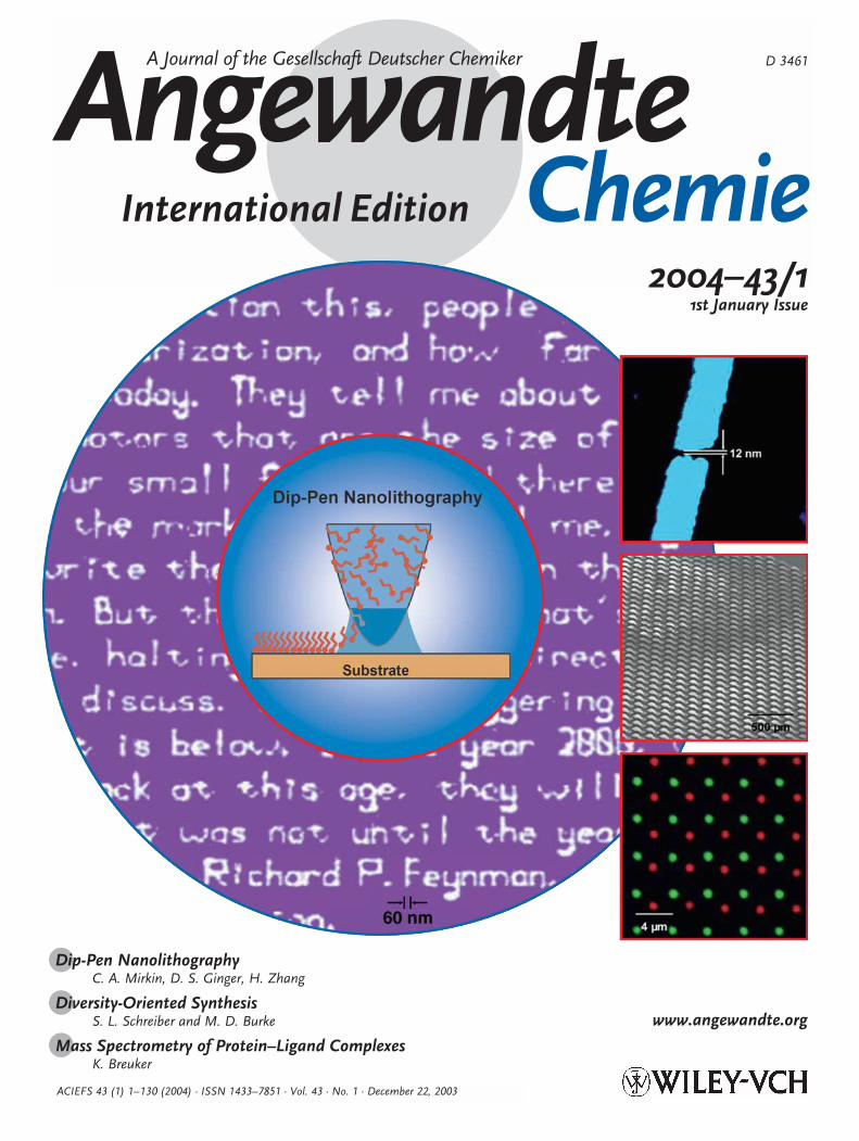
Nanolithography
The Evolution of Dip-Pen NanolithographyDavid S. Ginger, Hua Zhang, and Chad A. Mirkin*
AngewandteChemie
Keywords:biorecognition · dip-pennanolithography · microarrays ·nanostructures · surfacechemistry
C. A. Mirkin et al.Reviews
30 2004 Wiley-VCH Verlag GmbH & Co. KGaA, Weinheim DOI: 10.1002/anie.200300608 Angew. Chem. Int. Ed. 2004, 43, 30 – 45
1. Introduction
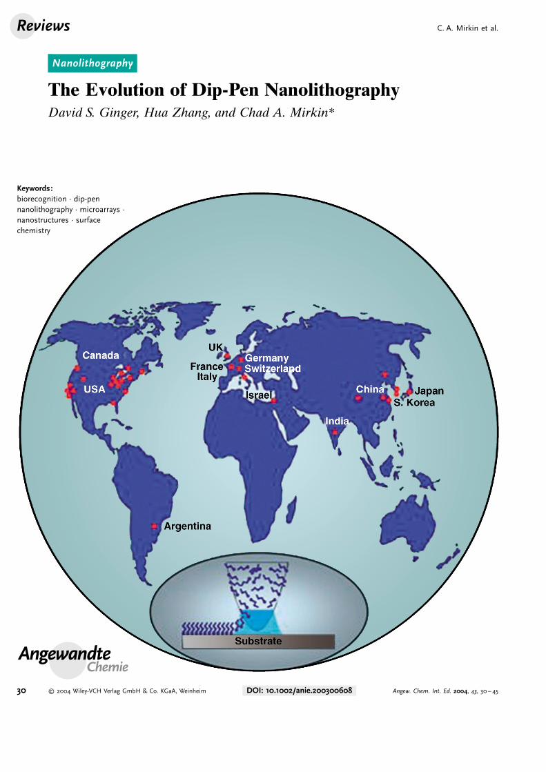
Developing methods that allow the chemistry of surfacesto be controlled on the 1–100 nm length scale is a fundamen-tal and exciting challenge in nanoscience and nanotechnologybecause it opens new possibilities in fields ranging frommolecular electronics to biomedicine to catalysis. This chal-lenge has motivated numerous researchers since the inventionof the scanning tunneling microscope (STM) and its descend-ents (including atomic force microscopy (AFM)). Elegantstructures have been painstakingly crafted—one molecule ata time—with serial STM systems operating under ultrahighvacuum (UHV) and at low temperatures. Other groups haveused STM- and AFM-based methods to oxidize, scrape, oretch nanostructures onto surfaces. Such techniques haveimportant applications but are generally limited to the growthof thin oxides on select metal and semiconductor surfaces, orto multistep etch-and-backfill procedures that cannot beeasily generalized to the parallel patterning of multicompo-nent nanostructures.In 1999 dip-pen nanolithography (DPN) was introduced
to the research community as a new tool for fabricatingnanostructures on surfaces.[1] DPN is a direct-write scanning-probe-based lithography in which an AFM tip is used todeliver chemical reagents directly to nanoscopic regions of atarget substrate (Figure 1). Early results showed that DPN
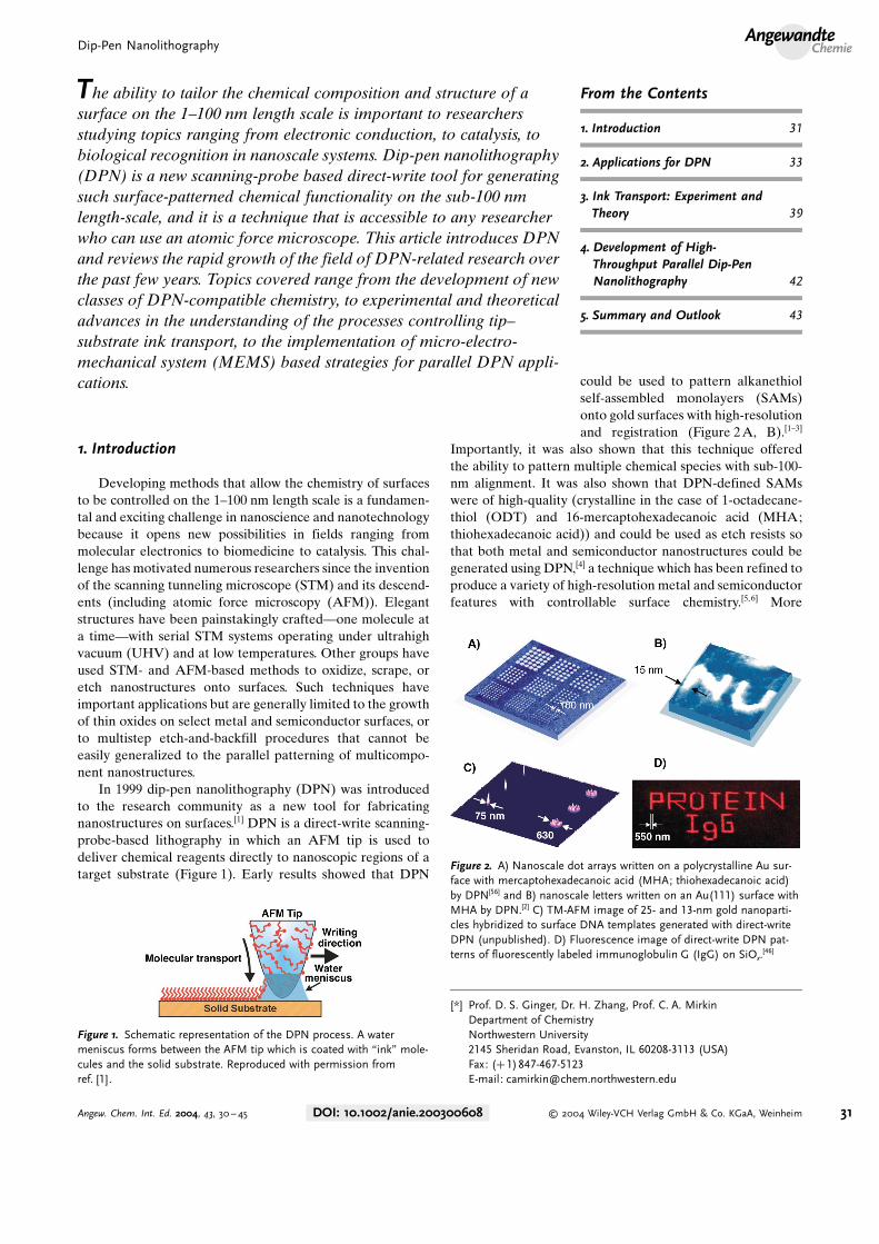
could be used to pattern alkanethiolself-assembled monolayers (SAMs)onto gold surfaces with high-resolutionand registration (Figure 2A, B).[1–3]
Importantly, it was also shown that this technique offeredthe ability to pattern multiple chemical species with sub-100-nm alignment. It was also shown that DPN-defined SAMswere of high-quality (crystalline in the case of 1-octadecane-thiol (ODT) and 16-mercaptohexadecanoic acid (MHA;thiohexadecanoic acid)) and could be used as etch resists sothat both metal and semiconductor nanostructures could begenerated using DPN,[4] a technique which has been refined toproduce a variety of high-resolution metal and semiconductorfeatures with controllable surface chemistry.[5,6] More
[*] Prof. D. S. Ginger, Dr. H. Zhang, Prof. C. A. MirkinDepartment of ChemistryNorthwestern University2145 Sheridan Road, Evanston, IL 60208-3113 (USA)Fax: (+1)847-467-5123E-mail: [email protected]
The ability to tailor the chemical composition and structure of asurface on the 1–100 nm length scale is important to researchersstudying topics ranging from electronic conduction, to catalysis, tobiological recognition in nanoscale systems. Dip-pen nanolithography(DPN) is a new scanning-probe based direct-write tool for generatingsuch surface-patterned chemical functionality on the sub-100 nmlength-scale, and it is a technique that is accessible to any researcherwho can use an atomic force microscope. This article introduces DPNand reviews the rapid growth of the field of DPN-related research overthe past few years. Topics covered range from the development of newclasses of DPN-compatible chemistry, to experimental and theoreticaladvances in the understanding of the processes controlling tip–substrate ink transport, to the implementation of micro-electro-mechanical system (MEMS) based strategies for parallel DPN appli-cations.
From the Contents
1. Introduction 31
2. Applications for DPN 33
3. Ink Transport: Experiment andTheory 39
4. Development of High-Throughput Parallel Dip-PenNanolithography 42
5. Summary and Outlook 43
Figure 1. Schematic representation of the DPN process. A watermeniscus forms between the AFM tip which is coated with “ink” mole-cules and the solid substrate. Reproduced with permission fromref. [1].
Figure 2. A) Nanoscale dot arrays written on a polycrystalline Au sur-face with mercaptohexadecanoic acid (MHA; thiohexadecanoic acid)by DPN[56] and B) nanoscale letters written on an Au(111) surface withMHA by DPN.[2] C) TM-AFM image of 25- and 13-nm gold nanoparti-cles hybridized to surface DNA templates generated with direct-writeDPN (unpublished). D) Fluorescence image of direct-write DPN pat-terns of fluorescently labeled immunoglobulin G (IgG) on SiOx.
[46]
Dip-Pen NanolithographyAngewandte
Chemie
31Angew. Chem. Int. Ed. 2004, 43, 30 – 45 DOI: 10.1002/anie.200300608 2004 Wiley-VCH Verlag GmbH & Co. KGaA, Weinheim
recently, DPN has been developed to pattern a variety of“ink–substrate” combinations. DPN is compatible with manyinks, from small organic molecules[1–7, 109–111] to organic[8–10] andbiological[11,12] polymers (Figure 2C, D), and from colloidalparticles[13,31,65] to metal ions[14–16] and sols.[17,18,112] DPN can beused to pattern surfaces ranging from metals to insulators andto pattern on top of functional monolayers adsorbed on avariety of surfaces. We have even shown that DPN can beused to feed monomers to a living-polymerization reaction ina site-specific fashion, thus opening the possibility of creatingand screening combinatorial arrays of polymer feature-s.[108]An overview of the various chemistries used and thesystems in which they have been applied are presented inTable 1. Many of these systems are discussed in more detail inSection 2.As perhaps the only lithographic technique that offers
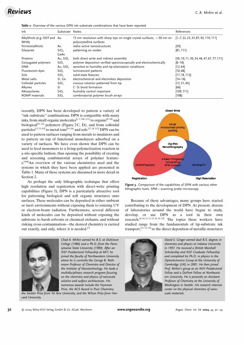
high resolution and registration with direct-write printingcapabilities (Figure 3), DPN is a particularly attractive toolfor patterning biological and soft organic structures ontosurfaces. These molecules can be deposited in either ambientor inert environments without exposing them to ionizing UVor electron-beam radiation. Furthermore, several differentkinds of molecules can be deposited without exposing thesubstrate to harsh solvents or chemical etchants, and withoutrisking cross-contamination—the desired chemistry is carriedout exactly, and only, where it is needed.[7]
Because of these advantages, many groups have startedcontributing to the development of DPN. At present, dozensof laboratories around the world have begun to study,develop, or use DPN as a tool in their ownresearch.[8,10,11,13,15,16,19–32] The topics these workers havestudied range from the fundamentals of tip-substrate inktransport,[21–23,33] to the direct deposition of metallic structures
Chad A. Mirkin earned his B.S. at DickinsonCollege (1986) and a Ph.D. from the Penn-sylvania State University (1989). After anNSF Postdoctoral Fellowship at MIT, hejoined the faculty of Northwestern Universitywhere he is currently the George B. Rath-mann Professor of Chemistry and Director ofthe Institute of Nanotechnology. He leads amultidisciplinary research program focusingon the chemistry and physics of nanoscalesolution and surface architectures. Hisnumerous awards include the FeynmanPrize, the ACS Award in Pure Chemistry,
the Sackler Prize from Tel Aviv University, and the Wilson Prize from Har-vard University.
David S. Ginger earned dual B.S. degrees inchemistry and physics at Indiana Universityin 1997. He received a British MarshallScholarship and NSF Graduate Fellowshipand completed his Ph.D. in physics in theOptoelectronics Group at the University ofCambridge (UK) in 2001. He then joinedProf. Mirkin's group as an NIH PostdoctoralFellow and a DuPont Fellow at Northwest-ern University. He is presently an AssistantProfessor of Chemistry at the University ofWashington in Seattle. His research interestscenter on the physical chemistry of nano-scale materials.
Table 1: Overview of the various DPN ink–substrate combinations that have been reported.
Ink Substrate Notes References
Alkylthiols (e.g. ODTandMHA)
Au 15 nm resolution with sharp tips on single crystal surfaces, <50 nm onpolycrystalline surfaces
[1–7,22,23,33,87,92,110,111]
Ferrocenylthiols Au redox active nanostructures [59]Silazanes SiOx,
GaAspatterning on oxides [81,111]
Proteins Au, SiOx both direct write and indirect assembly [3b,10,11,30,34,46,47,67,77,111]Conjugated polymers SiOx polymer deposition verified spectroscopically and electrochemically [8–10]DNA Au, SiOx sensitive to humidity and tip-silanization conditions [12,64]Fluorescent dyes SiOx luminescent patterns [10,68]Sols SiOx solid-state features [17,18,112]Metal salts Si, Ge electrochemical and electroless deposition [14–16]Colloidal particles SiOx viscous solution patterned from tip [13,31,65]Alkynes Si C�Si bond formation [66]Alkoxysilanes SiOx humidity control important [109,111]ROMP materials SiOx combinatorial polymer brush arrays [108]
Figure 3. Comparison of the capabilities of DPN with various otherlithographic tools. SPM=scanning probe microscopy.
C. A. Mirkin et al.Reviews
32 2004 Wiley-VCH Verlag GmbH & Co. KGaA, Weinheim www.angewandte.org Angew. Chem. Int. Ed. 2004, 43, 30 – 45
and development of electrochemical DPN,[8,15] to the depo-sition of biomolecules[12, 30,34] and the effects of DPN on theorganization of biopolymers.[11]
2. Applications for DPN
It is often difficult to predict the path of development thatan emerging technology will follow. However, a survey of therecent literature suggests several scientific and technologicalareas where DPN is likely to have an important impact(although there are certainly other uses waiting for aresearcher to perform the proof-of-concept and developmentexperiments). In this section we focus on four areas in whichwe believe the unique capabilities of DPN are particularlylikely to make an impact: patterning biomolecular micro- andnanoarrays (Section 2.1), building tailored chemical surfacesfor studying and controlling biorecognition processes fromthe molecular to cellular level (Section 2.2), generatingchemical templates for the controlled orthogonal assemblyof materials on surfaces (Section 2.3), and the use of DPN as arapid prototyping tool for generating hard nanostructuresusing chemical etching on a length-scale comparable, or evensuperior, to that obtainable with e-beam lithography (Sec-tion 2.4). The use of DPN for in situ studies of surfacereactivity and exchange chemistry is discussed separately inSection 3.
2.1. Biomolecular Micro- and Nanoarrays
As a direct-write technique, DPN is particularly well-suited for patterning biological molecules on surfaces. With aresolution limit orders of magnitude better than any alter-native robotic spotting or photolithographic technology, DPNhas the potential to revolutionize the technology of surface-based biomolecular assays, including array-based DNA, smallmolecule, and protein detection. Such chip-based array-format detection systems, or “microarrays,” have becomeubiquitous in almost all areas of health-related research.[35–41]
The power of cDNA and oligonucleotide arrays to quantifyboth gene expression and genomic structure (e.g. throughsingle-nucleotide-polymorphism (SNP) detection), has led totheir use in among others oncology,[38] infectious-disease
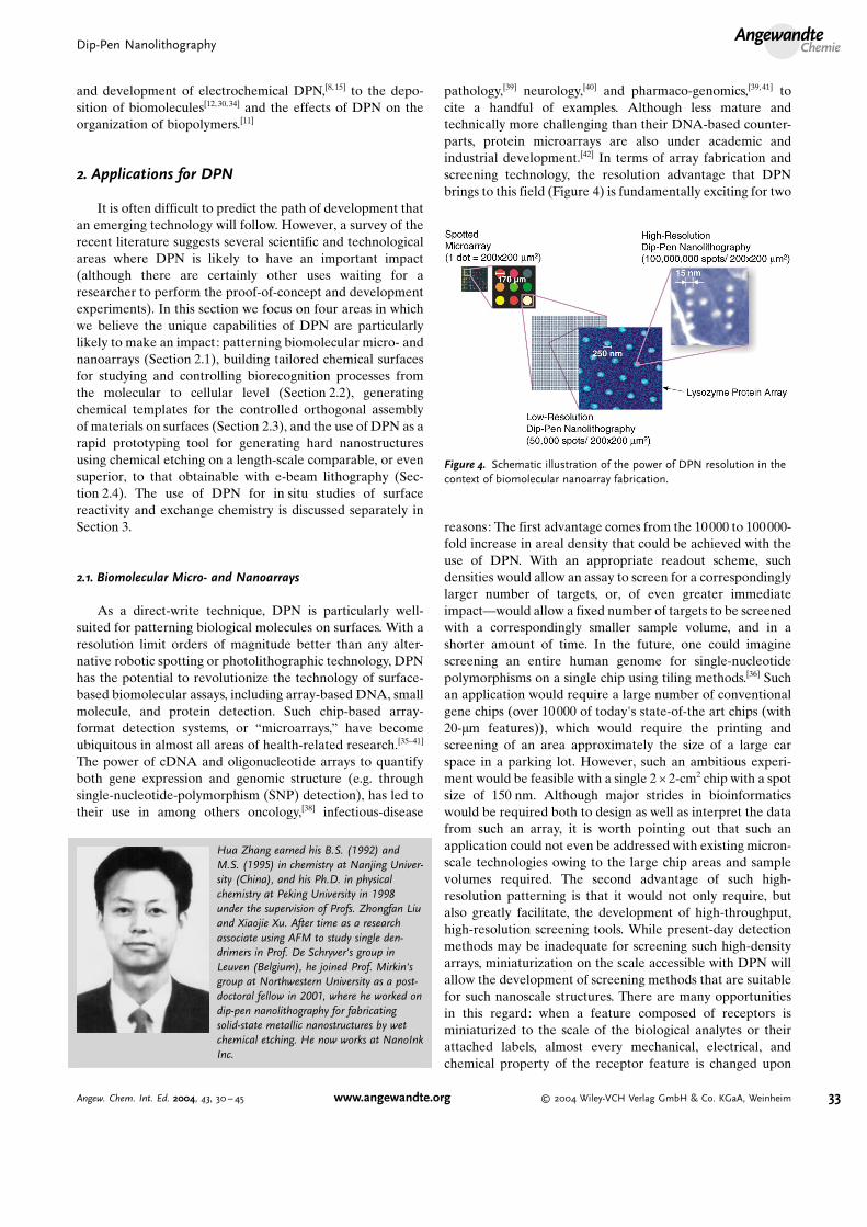
pathology,[39] neurology,[40] and pharmaco-genomics,[39,41] tocite a handful of examples. Although less mature andtechnically more challenging than their DNA-based counter-parts, protein microarrays are also under academic andindustrial development.[42] In terms of array fabrication andscreening technology, the resolution advantage that DPNbrings to this field (Figure 4) is fundamentally exciting for two
reasons: The first advantage comes from the 10000 to 100000-fold increase in areal density that could be achieved with theuse of DPN. With an appropriate readout scheme, suchdensities would allow an assay to screen for a correspondinglylarger number of targets, or, of even greater immediateimpact—would allow a fixed number of targets to be screenedwith a correspondingly smaller sample volume, and in ashorter amount of time. In the future, one could imaginescreening an entire human genome for single-nucleotidepolymorphisms on a single chip using tiling methods.[36] Suchan application would require a large number of conventionalgene chips (over 10000 of today's state-of-the art chips (with20-mm features)), which would require the printing andscreening of an area approximately the size of a large carspace in a parking lot. However, such an ambitious experi-ment would be feasible with a single 2 C 2-cm2 chip with a spotsize of 150 nm. Although major strides in bioinformaticswould be required both to design as well as interpret the datafrom such an array, it is worth pointing out that such anapplication could not even be addressed with existing micron-scale technologies owing to the large chip areas and samplevolumes required. The second advantage of such high-resolution patterning is that it would not only require, butalso greatly facilitate, the development of high-throughput,high-resolution screening tools. While present-day detectionmethods may be inadequate for screening such high-densityarrays, miniaturization on the scale accessible with DPN willallow the development of screening methods that are suitablefor such nanoscale structures. There are many opportunitiesin this regard: when a feature composed of receptors isminiaturized to the scale of the biological analytes or theirattached labels, almost every mechanical, electrical, andchemical property of the receptor feature is changed upon
Hua Zhang earned his B.S. (1992) andM.S. (1995) in chemistry at Nanjing Univer-sity (China), and his Ph.D. in physicalchemistry at Peking University in 1998under the supervision of Profs. Zhongfan Liuand Xiaojie Xu. After time as a researchassociate using AFM to study single den-drimers in Prof. De Schryver's group inLeuven (Belgium), he joined Prof. Mirkin'sgroup at Northwestern University as a post-doctoral fellow in 2001, where he worked ondip-pen nanolithography for fabricatingsolid-state metallic nanostructures by wetchemical etching. He now works at NanoInkInc.
Figure 4. Schematic illustration of the power of DPN resolution in thecontext of biomolecular nanoarray fabrication.
Dip-Pen NanolithographyAngewandte
Chemie
33Angew. Chem. Int. Ed. 2004, 43, 30 – 45 www.angewandte.org 2004 Wiley-VCH Verlag GmbH & Co. KGaA, Weinheim
reaction with the analyte. These properties, which includesize, shape, electrical conductivity, and hydrophilicity, all canbe monitored in situ with an AFM or with on-chip electroniccircuitry. In the long term, it may even be possible to directthe attachment of proteins and virus particles in specificorientations and thus to study reactivity as a function ofstructural configuration.To proceed along such a path towards miniaturization will
require obstacles to be overcome along the way. However, thepotential rewards clearly justify the effort. One potentialdifficulty comes from cross-reactivity and nonspecific binding(NSB) of analyte or other species to the array spots. AlthoughNSB is a problem for any surface-based assay, NSB is likely tobecome more problematic for screening on the nanoscale: ona nanoscale receptor spot it would be possible for a fewnonspecifically bound particles to completely overwhelm theintended signal. Fortunately, moving to the nanoscale offersnew possibilities to alleviate the NSB problem. On one hand,for a small sacrifice in information density, redundancy and“error checking” can be built into any array. On the otherhand, controlling (and screening) the chemical environmentwith nanoscale precision could offer the opportunity both toreduce the frequency of NSB events, and to more readilyidentify them when they do occur. Finally, because DPN is adirect-write technology, cross-contamination of the patternedarray features is entirely eliminated.Before any of the advantages of high-resolution array
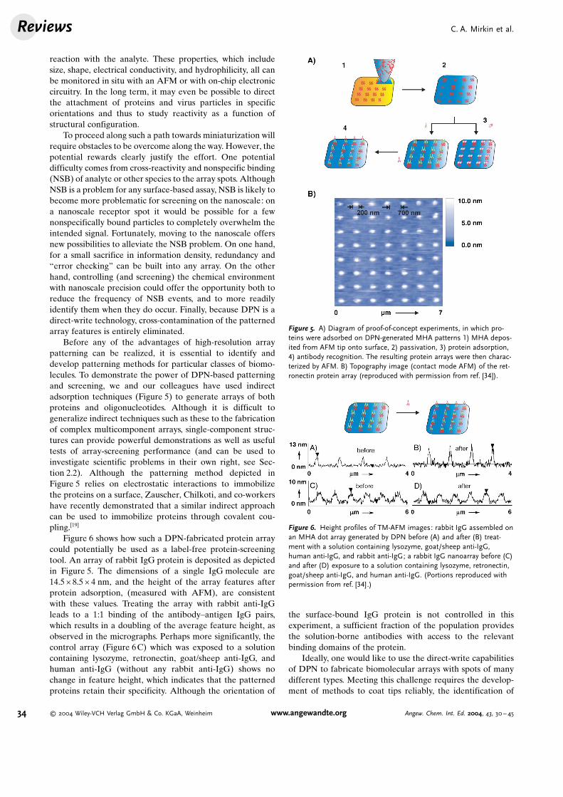
patterning can be realized, it is essential to identify anddevelop patterning methods for particular classes of biomo-lecules. To demonstrate the power of DPN-based patterningand screening, we and our colleagues have used indirectadsorption techniques (Figure 5) to generate arrays of bothproteins and oligonucleotides. Although it is difficult togeneralize indirect techniques such as these to the fabricationof complex multicomponent arrays, single-component struc-tures can provide powerful demonstrations as well as usefultests of array-screening performance (and can be used toinvestigate scientific problems in their own right, see Sec-tion 2.2). Although the patterning method depicted inFigure 5 relies on electrostatic interactions to immobilizethe proteins on a surface, Zauscher, Chilkoti, and co-workershave recently demonstrated that a similar indirect approachcan be used to immobilize proteins through covalent cou-pling.[19]
Figure 6 shows how such a DPN-fabricated protein arraycould potentially be used as a label-free protein-screeningtool. An array of rabbit IgG protein is deposited as depictedin Figure 5. The dimensions of a single IgG molecule are14.5 C 8.5 C 4 nm, and the height of the array features afterprotein adsorption, (measured with AFM), are consistentwith these values. Treating the array with rabbit anti-IgGleads to a 1:1 binding of the antibody–antigen IgG pairs,which results in a doubling of the average feature height, asobserved in the micrographs. Perhaps more significantly, thecontrol array (Figure 6C) which was exposed to a solutioncontaining lysozyme, retronectin, goat/sheep anti-IgG, andhuman anti-IgG (without any rabbit anti-IgG) shows nochange in feature height, which indicates that the patternedproteins retain their specificity. Although the orientation of
the surface-bound IgG protein is not controlled in thisexperiment, a sufficient fraction of the population providesthe solution-borne antibodies with access to the relevantbinding domains of the protein.Ideally, one would like to use the direct-write capabilities
of DPN to fabricate biomolecular arrays with spots of manydifferent types. Meeting this challenge requires the develop-ment of methods to coat tips reliably, the identification of
Figure 5. A) Diagram of proof-of-concept experiments, in which pro-teins were adsorbed on DPN-generated MHA patterns 1) MHA depos-ited from AFM tip onto surface, 2) passivation, 3) protein adsorption,4) antibody recognition. The resulting protein arrays were then charac-terized by AFM. B) Topography image (contact mode AFM) of the ret-ronectin protein array (reproduced with permission from ref. [34]).
Figure 6. Height profiles of TM-AFM images: rabbit IgG assembled onan MHA dot array generated by DPN before (A) and after (B) treat-ment with a solution containing lysozyme, goat/sheep anti-IgG,human anti-IgG, and rabbit anti-IgG; a rabbit IgG nanoarray before (C)and after (D) exposure to a solution containing lysozyme, retronectin,goat/sheep anti-IgG, and human anti-IgG. (Portions reproduced withpermission from ref. [34].)
C. A. Mirkin et al.Reviews
34 2004 Wiley-VCH Verlag GmbH & Co. KGaA, Weinheim www.angewandte.org Angew. Chem. Int. Ed. 2004, 43, 30 – 45
conditions for reproducible tip–substrate transport and ink–substrate coupling, and ultimately the implementation ofparallel-pen and integrated-inking systems. Because theMEMs challenges of parallel-pen and integrated-inkingsystems are covered more fully in Section 4, this section willfocus instead on the chemistry involved.We have used direct-write DPN to pattern oligonucleo-
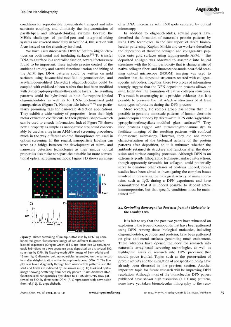
tides on both metal and insulating surfaces.[12] To transferDNA to a surface in a controlled fashion, several factors werefound to be important, these include precise control of theambient humidity and careful functionalization and inking ofthe AFM tips. DNA patterns could be written on goldsurfaces using hexanethiol-modified oligonucleotides, andacrylamide-modified (Acrydite) oligonucleotides could becoupled with oxidized silicon wafers that had been modifiedwith 3’-mercaptopropyltrimethoxysilane layers. The resultingpatterns could be hybridized to both fluorophore-labeledoligonucleotides as well as to DNA-functionalized goldnanoparticles (Figure 7). Nanoparticle labels[43–45] are partic-ularly promising tags for nanoscale detection applications.They exhibit a wide variety of properties—from their highmolar extinction coefficients, to their physical shapes—whichcan be used to encode information. Indeed Figure 7B showshow a property as simple as nanoparticle size could conceiv-ably be used as a tag in an AFM-based screening procedure,much in the way different colored fluorophores are used inoptical screening. In this regard, nanoparticle labeling canserve as a bridge between the development of micro- andnanoscale detection technologies as their unique opticalproperties also make nanoparticles suitable for more conven-tional optical screening methods: Figure 7D shows an image
of a DNA microarray with 1600 spots captured by opticalmicroscopy.In addition to oligonucleotides, several papers have
described the formation of nanoscale protein patterns byusing DPN techniques. In the first report of direct biomo-lecular patterning, Kaplan, Mirkin and co-workers describedthe deposition of thiolated collagen and collagen-like pep-tides onto gold surfaces using tapping-mode AFM.[11] Thedeposited collagen was observed to assemble into helicalstructures with the 65-nm periodicity that is characteristic ofnative collagen fiber, and fluorescence-mode near-field scan-ning optical microscopy (NSOM) imaging was used toconfirm that the deposited structures reacted with collagen-specific antibodies. Together, these two pieces of informationstrongly suggest that the DPN deposition process allows, oreven facilitates, the formation of native collagen structures.This result is encouraging as it provides evidence that it ispossible to preserve the native/active structures of at leastsome types of proteins during the DPN process.More recently, De Yoreo's group has shown that it is
possible to generate nanoscale patterns of human chorionicgonadotropin antibody by direct-write DPN onto 3-glycidox-ypropyltrimethoxysilane-modified glass surfaces.[10] Theyused proteins tagged with tetramethylrhodamine dye tofacilitate imaging of the resulting patterns with confocalfluorescence microscopy. However, they did not reportcharacterization of the biological activity of the proteinpatterns after deposition, so it is unknown whether theantibody retained its structure and function after the depo-sition and surface coupling processes. Although DPN is anextremely gentle lithographic technique, surface interactions,though apparently favorable for collagen, could potentiallyserve to denature other classes of proteins. Indeed, recentstudies have been aimed at investigating the complex issuesinvolved in preserving the biological activity of immunopro-teins, such as IgG, during a DPN experiment and havedemonstrated that it is indeed possible to deposit activeimmunoproteins, but that specific conditions must be main-tained.[46,47]
2.2. Controlling Biorecognition Processes from the Molecular tothe Cellular Level
It is fair to say that the past two years have witnessed anexplosion in the types of compounds that have been patternedusing DPN. Among these, biological molecules, includingoligonucleotides, peptides, and proteins, have been patternedon glass and metal surfaces, generating much excitement.These advances have opened the door for research intonanoscale array-based screening technologies, as well ashighlighted areas of research into DPN processes thatshould prove fruitful. Topics such as the preservation ofprotein activity and the mitigation of nonspecific binding havealready been discussed in the previous section. Anotherimportant topic for future research will be improving DPNresolution. Although most of the biomolecular DPN paperspublished have shown high-resolution (� 100 nm) patterns,none have yet taken biomolecular lithography to the reso-
Figure 7. Direct patterning of multiple-DNA inks by DPN. A) Com-bined red–green fluorescence image of two different fluorophore-labeled sequences (Oregon Green 488-X and Texas Red-X) simultane-ously hybridized to a two-sequence array deposited on a silanized SiOx
substrate by DPN. B) Tapping-mode AFM image of 5-nm (dark) and13-nm (light) diameter gold nanoparticles assembled on the same pat-tern after dehybridization of the fluorophore-labeled DNA. C) The lineplot was taken diagonally through both nanoparticle patterns, and thestart and finish are indicated by the arrows in (B). D) Darkfield opitcalimage showing scattering from densely packed 13-nm diameter DNA-functionalized nanoparticles hybridized to a 1600-dot DNA array pat-terned on SiOx by direct-write DPN. (A–C reproduced with permissionfrom ref. [12], D, unpublished).
Dip-Pen NanolithographyAngewandte
Chemie
35Angew. Chem. Int. Ed. 2004, 43, 30 – 45 www.angewandte.org 2004 Wiley-VCH Verlag GmbH & Co. KGaA, Weinheim
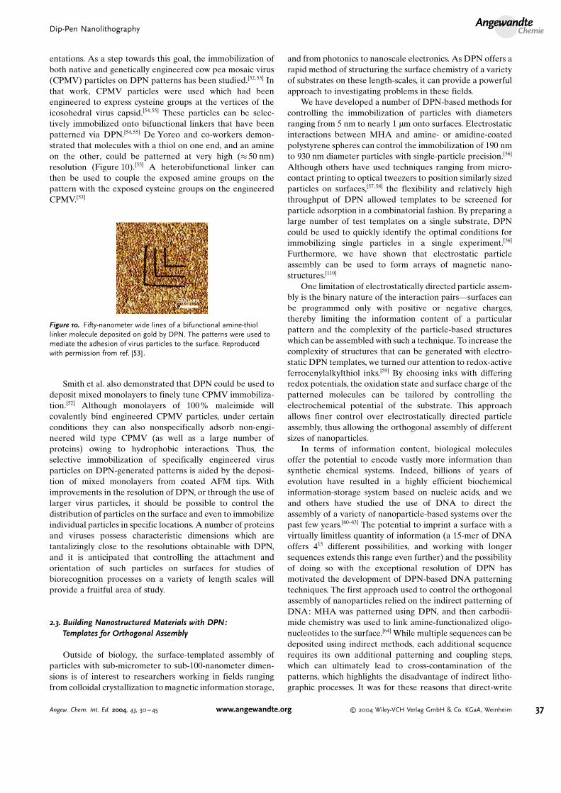
lution obtainable at the cutting-edge of DPN technology(currently � 15 nm for alkanethiol inks on single-crystal goldsurfaces).[2] Such sizes are commensurate with the size ofindividual biological macromolecules, which offers the tanta-lizing possibility that DPN could be used to positionindividual structures with molecular resolution to createtailored chemical surfaces that would allow the investigationof a variety of biological recognition processes spanning themolecular to the cellular level. The development of evenhigher-resolution DPN techniques may require the use ofhigh aspect ratio AFM tips (such as carbon nanotubes[48]) orthe combination of DPN with techniques such as nanograft-ing. The DPN–nanografting combination was described byG.-y. Liu and co-workers in a method they call the “nanopen-reader-writer” (NPRW) (Figure 8).[20,49] NPRW employs a
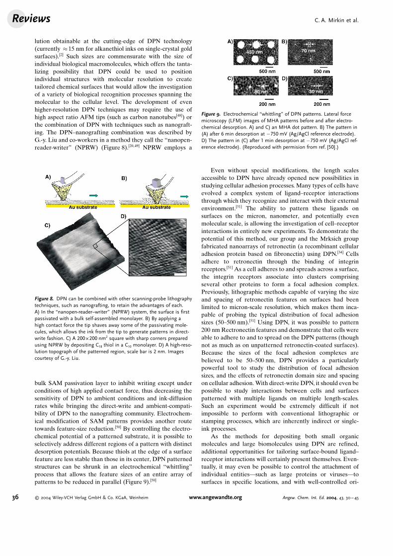
bulk SAM passivation layer to inhibit writing except underconditions of high applied contact force, thus decreasing thesensitivity of DPN to ambient conditions and ink-diffusionrates while bringing the direct-write and ambient-compati-bility of DPN to the nanografting community. Electrochem-ical modification of SAM patterns provides another routetowards feature-size reduction.[50] By controlling the electro-chemical potential of a patterned substrate, it is possible toselectively address different regions of a pattern with distinctdesorption potentials. Because thiols at the edge of a surfacefeature are less stable than those in its center, DPN patternedstructures can be shrunk in an electrochemical “whittling”process that allows the feature sizes of an entire array ofpatterns to be reduced in parallel (Figure 9).[50]
Even without special modifications, the length scalesaccessible to DPN have already opened new possibilities instudying cellular adhesion processes. Many types of cells haveevolved a complex system of ligand–receptor interactionsthrough which they recognize and interact with their externalenvironment.[51] The ability to pattern these ligands onsurfaces on the micron, nanometer, and potentially evenmolecular scale, is allowing the investigation of cell–receptorinteractions in entirely new experiments. To demonstrate thepotential of this method, our group and the Mrksich groupfabricated nanoarrays of retronectin (a recombinant cellularadhesion protein based on fibronectin) using DPN.[34] Cellsadhere to retronectin through the binding of integrinreceptors.[51] As a cell adheres to and spreads across a surface,the integrin receptors associate into clusters comprisingseveral other proteins to form a focal adhesion complex.Previously, lithographic methods capable of varying the sizeand spacing of retronectin features on surfaces had beenlimited to micron-scale resolution, which makes them inca-pable of probing the typical distribution of focal adhesionsizes (50–500 nm).[51] Using DPN, it was possible to pattern200 nmRectronectin features and demonstrate that cells wereable to adhere to and to spread on the DPN patterns (thoughnot as much as on unpatterned retronectin-coated surfaces).Because the sizes of the focal adhesion complexes arebelieved to be 50–500 nm, DPN provides a particularlypowerful tool to study the distribution of focal adhesionsizes, and the effects of retronectin domain size and spacingon cellular adhesion.With direct-write DPN, it should even bepossible to study interactions between cells and surfacespatterned with multiple ligands on multiple length-scales.Such an experiment would be extremely difficult if notimpossible to perform with conventional lithographic orstamping processes, which are inherently indirect or single-ink processes.As the methods for depositing both small organic
molecules and large biomolecules using DPN are refined,additional opportunities for tailoring surface-bound ligand–receptor interactions will certainly present themselves. Even-tually, it may even be possible to control the attachment ofindividual entities—such as large proteins or viruses—tosurfaces in specific locations, and with well-controlled ori-
Figure 8. DPN can be combined with other scanning-probe lithographytechniques, such as nanografting, to retain the advantages of each.A) In the “nanopen-reader–writer” (NPRW) system, the surface is firstpassivated with a bulk self-assembled monolayer. B) By applying ahigh contact force the tip shaves away some of the passivating mole-cules, which allows the ink from the tip to generate patterns in direct-write fashion. C) A 200J200 nm2 square with sharp corners preparedusing NPRW by depositing C18 thiol in a C10 monolayer. D) A high-reso-lution topograph of the patterned region, scale bar is 2 nm. Imagescourtesy of G.-y. Liu.
Figure 9. Electrochemical “whittling” of DPN patterns. Lateral forcemicroscopy (LFM) images of MHA patterns before and after electro-chemical desorption. A) and C) an MHA dot pattern. B) The pattern in(A) after 6 min desorption at �750 mV (Ag/AgCl reference electrode).D) The pattern in (C) after 1 min desorption at �750 mV (Ag/AgCl ref-erence electrode). (Reproduced with permision from ref. [50].)
C. A. Mirkin et al.Reviews
36 2004 Wiley-VCH Verlag GmbH & Co. KGaA, Weinheim www.angewandte.org Angew. Chem. Int. Ed. 2004, 43, 30 – 45
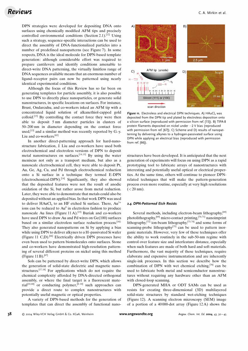
entations. As a step towards this goal, the immobilization ofboth native and genetically engineered cow pea mosaic virus(CPMV) particles on DPN patterns has been studied.[52,53] Inthat work, CPMV particles were used which had beenengineered to express cysteine groups at the vertices of theicosohedral virus capsid.[54,55] These particles can be selec-tively immobilized onto bifunctional linkers that have beenpatterned via DPN.[54,55] De Yoreo and co-workers demon-strated that molecules with a thiol on one end, and an amineon the other, could be patterned at very high (� 50 nm)resolution (Figure 10).[53] A heterobifunctional linker canthen be used to couple the exposed amine groups on thepattern with the exposed cysteine groups on the engineeredCPMV.[53]
Smith et al. also demonstrated that DPN could be used todeposit mixed monolayers to finely tune CPMV immobiliza-tion.[52] Although monolayers of 100% maleimide willcovalently bind engineered CPMV particles, under certainconditions they can also nonspecifically adsorb non-engi-neered wild type CPMV (as well as a large number ofproteins) owing to hydrophobic interactions. Thus, theselective immobilization of specifically engineered virusparticles on DPN-generated patterns is aided by the deposi-tion of mixed monolayers from coated AFM tips. Withimprovements in the resolution of DPN, or through the use oflarger virus particles, it should be possible to control thedistribution of particles on the surface and even to immobilizeindividual particles in specific locations. A number of proteinsand viruses possess characteristic dimensions which aretantalizingly close to the resolutions obtainable with DPN,and it is anticipated that controlling the attachment andorientation of such particles on surfaces for studies ofbiorecognition processes on a variety of length scales willprovide a fruitful area of study.
2.3. Building Nanostructured Materials with DPN:Templates for Orthogonal Assembly
Outside of biology, the surface-templated assembly ofparticles with sub-micrometer to sub-100-nanometer dimen-sions is of interest to researchers working in fields rangingfrom colloidal crystallization to magnetic information storage,
and from photonics to nanoscale electronics. As DPN offers arapid method of structuring the surface chemistry of a varietyof substrates on these length-scales, it can provide a powerfulapproach to investigating problems in these fields.We have developed a number of DPN-based methods for
controlling the immobilization of particles with diametersranging from 5 nm to nearly 1 mm onto surfaces. Electrostaticinteractions between MHA and amine- or amidine-coatedpolystyrene spheres can control the immobilization of 190 nmto 930 nm diameter particles with single-particle precision.[56]
Although others have used techniques ranging from micro-contact printing to optical tweezers to position similarly sizedparticles on surfaces,[57, 58] the flexibility and relatively highthroughput of DPN allowed templates to be screened forparticle adsorption in a combinatorial fashion. By preparing alarge number of test templates on a single substrate, DPNcould be used to quickly identify the optimal conditions forimmobilizing single particles in a single experiment.[56]
Furthermore, we have shown that electrostatic particleassembly can be used to form arrays of magnetic nano-structures.[110]
One limitation of electrostatically directed particle assem-bly is the binary nature of the interaction pairs—surfaces canbe programmed only with positive or negative charges,thereby limiting the information content of a particularpattern and the complexity of the particle-based structureswhich can be assembled with such a technique. To increase thecomplexity of structures that can be generated with electro-static DPN templates, we turned our attention to redox-activeferrocenylalkylthiol inks.[59] By choosing inks with differingredox potentials, the oxidation state and surface charge of thepatterned molecules can be tailored by controlling theelectrochemical potential of the substrate. This approachallows finer control over electrostatically directed particleassembly, thus allowing the orthogonal assembly of differentsizes of nanoparticles.In terms of information content, biological molecules
offer the potential to encode vastly more information thansynthetic chemical systems. Indeed, billions of years ofevolution have resulted in a highly efficient biochemicalinformation-storage system based on nucleic acids, and weand others have studied the use of DNA to direct theassembly of a variety of nanoparticle-based systems over thepast few years.[60–63] The potential to imprint a surface with avirtually limitless quantity of information (a 15-mer of DNAoffers 415 different possibilities, and working with longersequences extends this range even further) and the possibilityof doing so with the exceptional resolution of DPN hasmotivated the development of DPN-based DNA patterningtechniques. The first approach used to control the orthogonalassembly of nanoparticles relied on the indirect patterning ofDNA: MHA was patterned using DPN, and then carbodii-mide chemistry was used to link amine-functionalized oligo-nucleotides to the surface.[64] While multiple sequences can bedeposited using indirect methods, each additional sequencerequires its own additional patterning and coupling steps,which can ultimately lead to cross-contamination of thepatterns, which highlights the disadvantage of indirect litho-graphic processes. It was for these reasons that direct-write
Figure 10. Fifty-nanometer wide lines of a bifunctional amine-thiollinker molecule deposited on gold by DPN. The patterns were used tomediate the adhesion of virus particles to the surface. Reproducedwith permission from ref. [53].
Dip-Pen NanolithographyAngewandte
Chemie
37Angew. Chem. Int. Ed. 2004, 43, 30 – 45 www.angewandte.org 2004 Wiley-VCH Verlag GmbH & Co. KGaA, Weinheim
DPN strategies were developed for depositing DNA ontosurfaces using chemically modified AFM tips and preciselycontrolled environmental conditions (Section 2.1).[12] Usingsuch a strategy, sequence-specific interactions can be used todirect the assembly of DNA-functionalized particles into anumber of predefined nanopatterns (see Figure 7). In somerespects, DNA is the ideal molecule for DPN-based templategeneration: although considerable effort was required toprepare cantilevers and identify conditions amenable todirect-write DNA patterning, the virtually limitless range ofDNA sequences available means that an enormous number ofligand–receptor pairs can now be patterned using nearlyidentical experimental conditions.Although the focus of this Review has so far been on
generating templates for particle assembly, it is also possibleto use DPN to directly place nanoparticles, or generate solidnanostructures, in specific locations on surfaces. For instance,Brust, Ondarcuhu, and co-workers inked an AFM tip with aconcentrated liquid solution of alkanethiol-capped goldcolloid.[13] By controlling the contact force they were thenable to deposit 5 nm diameter particles in clusters of50–200 nm in diameter depending on the contact forceused,[13] and a similar method was recently reported by G.-y.Liu and co-workers.[65]
In another direct-patterning approach for hard-nano-structure fabrication, J. Liu and co-workers have used bothelectrochemical and electroless versions of DPN to depositmetal nanostructures on surfaces.[14,15] By using the watermeniscus not only as a transport medium, but also as ananoscale electrochemical cell, they were able to deposit Pt,Au, Ge, Ag, Cu, and Pd through electrochemical reductiononto a Si surface in a technique they termed E-DPN(electrochemical-DPN).[14] Significantly, they also showedthat the deposited features were not the result of anodicoxidation of the Si, but rather arose from metal reduction.Later, they were able to demonstrate that metals could also bedeposited without an applied bias. In that work DPNwas usedto deliver HAuCl4 to an HF etched Si surface. There, Au
3+
ions can be reduced to Au0 in electroless fashion to producenanoscale Au lines (Figure 11A).[15] Buriak and co-workershave used DPN to draw Au and Pd wires on Ge(100) surfacesbased on a similar electroless surface reduction process.[16]-
They also generated nanopatterns on Si by applying a biaswhile using DPN to deliver alkynes to a H–passivated Si wafer(Figure 11 C,D).[66] Electrically driven DPN processes haveeven been used to pattern biomolecules onto surfaces. Stoneand co-workers have demonstrated high-resolution pattern-ing of several different proteins on nickel using this method(Figure 11B).[67]
Sols can be patterned by direct-write DPN, which allowsthe generation of solid-state dielectric and magnetic nano-structures.[17, 18] For applications which do not require thechemical complexity afforded by DNA-directed orthogonalassembly, or where the final target is a fluorescent mate-rial[10,68] or conducting polymer,[8–10] such approaches canprovide a direct route to complex nanostructures withpotentially useful magnetic or optical properties.A variety of DPN-based methods for the generation of
templates that can direct the assembly of functional nano-
structures have been developed. It is anticipated that the nextgeneration of experiments will focus on using DPN as a rapidprototyping tool to fabricate arrays of nanostructures withinteresting and potentially useful optical or electrical proper-ties. At the same time, others will continue to pioneer DPN-related techniques that will make the pattern-generationprocess even more routine, especially at very high resolutions(< 20 nm).
2.4. DPN-Patterned Etch Resists
Several methods, including electron-beam lithography,[69]
photolithography,[69] micro-contact printing,[70,71] nanoimprintlithography,[72] ion-beam lithography,[73,74] and some forms ofscanning-probe lithography[75] can be used to pattern inor-ganic materials. However, very few of these techniques offerthe ability to work routinely in the sub-50-nm regime withcontrol over feature size and interfeature distance, especiallywhen such features are made of both hard and soft materials.Furthermore, the vast majority of these techniques, requireelaborate and expensive instrumentation and are inherentlysingle-ink processes. In this section we describe how thecombination of DPN with wet chemical etching,[76] can beused to fabricate both metal and semiconductor nanostruc-tures without requiring any hardware other than an AFMwith closed-loop scanning.DPN-generated MHA or ODT SAMs can be used as
resists for creating three-dimensional (3D) multilayeredsolid-state structures by standard wet-etching techniques(Figure 12). A scanning electron microscopy (SEM) imageof a portion of a 40000-dot array (Figure 12A) shows the
Figure 11. Electroless and electrical DPN techniques. A) HAuCl4 wasdeposited from the DPN tip and plated by electroless deposition ontoa silicon surface (reproduced with permission from ref. [15]). B) TlPA-8protein filaments deposited on nickel under �2 V bias (reproducedwith permission from ref. [67]). C) Scheme and D) results of nanopat-terning by delivering alkynes to a hydrogen-passivated surface usingDPN while applying an electrical bias (reproduced with permissionfrom ref. [66]).
C. A. Mirkin et al.Reviews
38 2004 Wiley-VCH Verlag GmbH & Co. KGaA, Weinheim www.angewandte.org Angew. Chem. Int. Ed. 2004, 43, 30 – 45
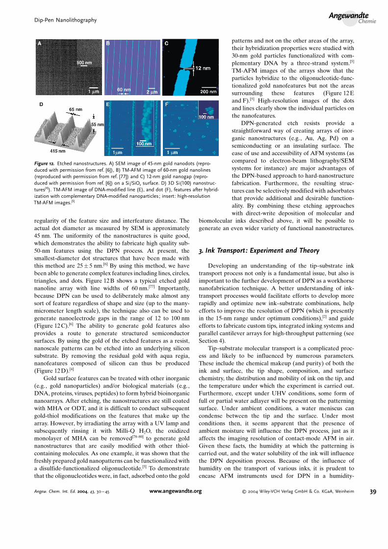
regularity of the feature size and interfeature distance. Theactual dot diameter as measured by SEM is approximately45 nm. The uniformity of the nanostructures is quite good,which demonstrates the ability to fabricate high quality sub-50-nm features using the DPN process. At present, thesmallest-diameter dot structures that have been made withthis method are 25� 5 nm.[6] By using this method, we havebeen able to generate complex features including lines, circles,triangles, and dots. Figure 12B shows a typical etched goldnanoline array with line widths of 60 nm.[77] Importantly,because DPN can be used to deliberately make almost anysort of feature regardless of shape and size (up to the many-micrometer length scale), the technique also can be used togenerate nanoelectrode gaps in the range of 12 to 100 nm(Figure 12C).[6] The ability to generate gold features alsoprovides a route to generate structured semiconductorsurfaces. By using the gold of the etched features as a resist,nanoscale patterns can be etched into an underlying siliconsubstrate. By removing the residual gold with aqua regia,nanofeatures composed of silicon can thus be produced(Figure 12D).[4]
Gold surface features can be treated with other inorganic(e.g., gold nanoparticles) and/or biological materials (e.g.,DNA, proteins, viruses, peptides) to form hybrid bioinorganicnanoarrays. After etching, the nanostructures are still coatedwith MHA or ODT, and it is difficult to conduct subsequentgold-thiol modifications on the features that make up thearray. However, by irradiating the array with a UV lamp andsubsequently rinsing it with Milli-Q H2O, the oxidizedmonolayer of MHA can be removed[78–80] to generate goldnanostructures that are easily modified with other thiol-containing molecules. As one example, it was shown that thefreshly prepared gold nanopatterns can be functionalized witha disulfide-functionalized oligonucleotide.[5] To demonstratethat the oligonucleotides were, in fact, adsorbed onto the gold
patterns and not on the other areas of the array,their hybridization properties were studied with30-nm gold particles functionalized with com-plementary DNA by a three-strand system.[5]
TM-AFM images of the arrays show that theparticles hybridize to the oligonucleotide-func-tionalized gold nanofeatures but not the areassurrounding these features (Figure 12Eand F).[5] High-resolution images of the dotsand lines clearly show the individual particles onthe nanofeatures.DPN-generated etch resists provide a
straightforward way of creating arrays of inor-ganic nanostructures (e.g., Au, Ag, Pd) on asemiconducting or an insulating surface. Theease of use and accessibility of AFM systems (ascompared to electron-beam lithography/SEMsystems for instance) are major advantages ofthe DPN-based approach to hard-nanostructurefabrication. Furthermore, the resulting struc-tures can be selectively modified with adsorbatesthat provide additional and desirable function-ality. By combining these etching approacheswith direct-write deposition of molecular and
biomolecular inks described above, it will be possible togenerate an even wider variety of functional nanostructures.
3. Ink Transport: Experiment and Theory
Developing an understanding of the tip–substrate inktransport process not only is a fundamental issue, but also isimportant to the further development of DPN as a workhorsenanofabrication technique. A better understanding of ink-transport processes would facilitate efforts to develop morerapidly and optimize new ink–substrate combinations, helpefforts to improve the resolution of DPN (which is presentlyin the 15-nm range under optimum conditions),[2] and guideefforts to fabricate custom tips, integrated inking systems andparallel cantilever arrays for high-throughput patterning (seeSection 4).Tip–substrate molecular transport is a complicated proc-
ess and likely to be influenced by numerous parameters.These include the chemical makeup (and purity) of both theink and surface, the tip shape, composition, and surfacechemistry, the distribution and mobility of ink on the tip, andthe temperature under which the experiment is carried out.Furthermore, except under UHV conditions, some form offull or partial water adlayer will be present on the patterningsurface. Under ambient conditions, a water meniscus cancondense between the tip and the surface. Under mostconditions then, it seems apparent that the presence ofambient moisture will influence the DPN process, just as itaffects the imaging resolution of contact-mode AFM in air.Given these facts, the humidity at which the patterning iscarried out, and the water solubility of the ink will influencethe DPN deposition process. Because of the influence ofhumidity on the transport of various inks, it is prudent toencase AFM instruments used for DPN in a humidity-
Figure 12. Etched nanostructures. A) SEM image of 45-nm gold nanodots (repro-duced with permission from ref. [6]), B) TM-AFM image of 60-nm gold nanolines(reproduced with permission from ref. [77]) and C) 12-nm gold nanogap (repro-duced with permission from ref. [6]) on a Si/SiOx surface. D) 3D Si(100) nanostruc-tures[4]). TM-AFM image of DNA-modified line (E), and dot (F), features after hybrid-ization with complementary DNA-modified nanoparticles; insert: high-resolutionTM-AFM images.[5]
Dip-Pen NanolithographyAngewandte
Chemie
39Angew. Chem. Int. Ed. 2004, 43, 30 – 45 www.angewandte.org 2004 Wiley-VCH Verlag GmbH & Co. KGaA, Weinheim
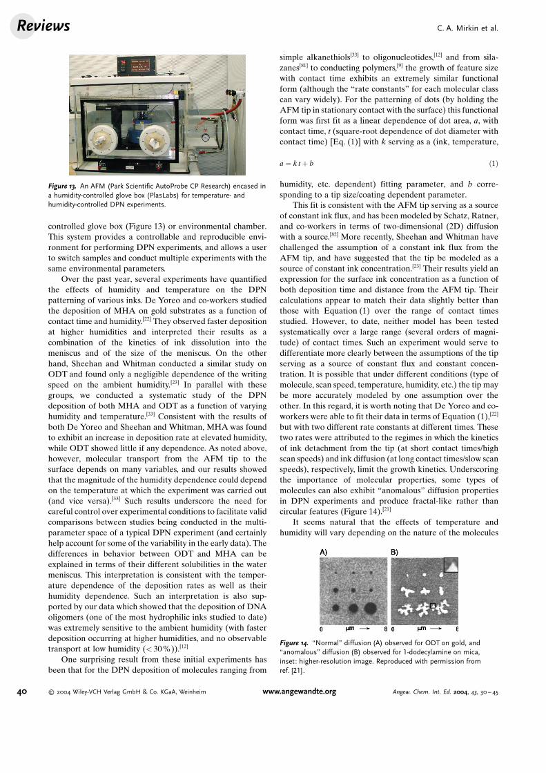
controlled glove box (Figure 13) or environmental chamber.This system provides a controllable and reproducible envi-ronment for performing DPN experiments, and allows a userto switch samples and conduct multiple experiments with thesame environmental parameters.Over the past year, several experiments have quantified
the effects of humidity and temperature on the DPNpatterning of various inks. De Yoreo and co-workers studiedthe deposition of MHA on gold substrates as a function ofcontact time and humidity.[22] They observed faster depositionat higher humidities and interpreted their results as acombination of the kinetics of ink dissolution into themeniscus and of the size of the meniscus. On the otherhand, Sheehan and Whitman conducted a similar study onODT and found only a negligible dependence of the writingspeed on the ambient humidity.[23] In parallel with thesegroups, we conducted a systematic study of the DPNdeposition of both MHA and ODT as a function of varyinghumidity and temperature.[33] Consistent with the results ofboth De Yoreo and Sheehan and Whitman, MHAwas foundto exhibit an increase in deposition rate at elevated humidity,while ODT showed little if any dependence. As noted above,however, molecular transport from the AFM tip to thesurface depends on many variables, and our results showedthat the magnitude of the humidity dependence could dependon the temperature at which the experiment was carried out(and vice versa).[33] Such results underscore the need forcareful control over experimental conditions to facilitate validcomparisons between studies being conducted in the multi-parameter space of a typical DPN experiment (and certainlyhelp account for some of the variability in the early data). Thedifferences in behavior between ODT and MHA can beexplained in terms of their different solubilities in the watermeniscus. This interpretation is consistent with the temper-ature dependence of the deposition rates as well as theirhumidity dependence. Such an interpretation is also sup-ported by our data which showed that the deposition of DNAoligomers (one of the most hydrophilic inks studied to date)was extremely sensitive to the ambient humidity (with fasterdeposition occurring at higher humidities, and no observabletransport at low humidity (< 30%)).[12]
One surprising result from these initial experiments hasbeen that for the DPN deposition of molecules ranging from
simple alkanethiols[33] to oligonucleotides,[12] and from sila-zanes[81] to conducting polymers,[9] the growth of feature sizewith contact time exhibits an extremely similar functionalform (although the “rate constants” for each molecular classcan vary widely). For the patterning of dots (by holding theAFM tip in stationary contact with the surface) this functionalform was first fit as a linear dependence of dot area, a, withcontact time, t (square-root dependence of dot diameter withcontact time) [Eq. (1)] with k serving as a (ink, temperature,
a ¼ k t þ b ð1Þ
humidity, etc. dependent) fitting parameter, and b corre-sponding to a tip size/coating dependent parameter.This fit is consistent with the AFM tip serving as a source
of constant ink flux, and has been modeled by Schatz, Ratner,and co-workers in terms of two-dimensional (2D) diffusionwith a source.[82] More recently, Sheehan and Whitman havechallenged the assumption of a constant ink flux from theAFM tip, and have suggested that the tip be modeled as asource of constant ink concentration.[23] Their results yield anexpression for the surface ink concentration as a function ofboth deposition time and distance from the AFM tip. Theircalculations appear to match their data slightly better thanthose with Equation (1) over the range of contact timesstudied. However, to date, neither model has been testedsystematically over a large range (several orders of magni-tude) of contact times. Such an experiment would serve todifferentiate more clearly between the assumptions of the tipserving as a source of constant flux and constant concen-tration. It is possible that under different conditions (type ofmolecule, scan speed, temperature, humidity, etc.) the tip maybe more accurately modeled by one assumption over theother. In this regard, it is worth noting that De Yoreo and co-workers were able to fit their data in terms of Equation (1),[22]
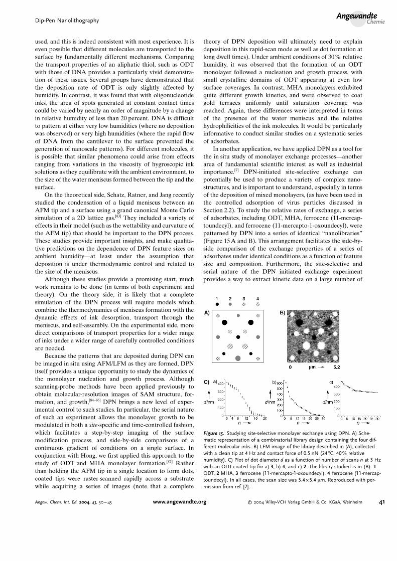
but with two different rate constants at different times. Thesetwo rates were attributed to the regimes in which the kineticsof ink detachment from the tip (at short contact times/highscan speeds) and ink diffusion (at long contact times/slow scanspeeds), respectively, limit the growth kinetics. Underscoringthe importance of molecular properties, some types ofmolecules can also exhibit “anomalous” diffusion propertiesin DPN experiments and produce fractal-like rather thancircular features (Figure 14).[21]
It seems natural that the effects of temperature andhumidity will vary depending on the nature of the molecules
Figure 13. An AFM (Park Scientific AutoProbe CP Research) encased ina humidity-controlled glove box (PlasLabs) for temperature- andhumidity-controlled DPN experiments.
Figure 14. “Normal” diffusion (A) observed for ODT on gold, and“anomalous” diffusion (B) observed for 1-dodecylamine on mica,inset: higher-resolution image. Reproduced with permission fromref. [21].
C. A. Mirkin et al.Reviews
40 2004 Wiley-VCH Verlag GmbH & Co. KGaA, Weinheim www.angewandte.org Angew. Chem. Int. Ed. 2004, 43, 30 – 45
used, and this is indeed consistent with most experience. It iseven possible that different molecules are transported to thesurface by fundamentally different mechanisms. Comparingthe transport properties of an aliphatic thiol, such as ODTwith those of DNA provides a particularly vivid demonstra-tion of these issues. Several groups have demonstrated thatthe deposition rate of ODT is only slightly affected byhumidity. In contrast, it was found that with oligonucleotideinks, the area of spots generated at constant contact timescould be varied by nearly an order of magnitude by a changein relative humidity of less than 20 percent. DNA is difficultto pattern at either very low humidities (where no depositionwas observed) or very high humidities (where the rapid flowof DNA from the cantilever to the surface prevented thegeneration of nanoscale patterns). For different molecules, itis possible that similar phenomena could arise from effectsranging from variations in the viscosity of hygroscopic inksolutions as they equilibrate with the ambient environment, tothe size of the water meniscus formed between the tip and thesurface.On the theoretical side, Schatz, Ratner, and Jang recently
studied the condensation of a liquid meniscus between anAFM tip and a surface using a grand canonical Monte Carlosimulation of a 2D lattice gas.[83] They included a variety ofeffects in their model (such as the wettability and curvature ofthe AFM tip) that should be important to the DPN process.These studies provide important insights, and make qualita-tive predictions on the dependence of DPN feature sizes onambient humidity—at least under the assumption thatdeposition is under thermodynamic control and related tothe size of the meniscus.Although these studies provide a promising start, much
work remains to be done (in terms of both experiment andtheory). On the theory side, it is likely that a completesimulation of the DPN process will require models whichcombine the thermodynamics of meniscus formation with thedynamic effects of ink desorption, transport through themeniscus, and self-assembly. On the experimental side, moredirect comparisons of transport properties for a wider rangeof inks under a wider range of carefully controlled conditionsare needed.Because the patterns that are deposited during DPN can
be imaged in situ using AFM/LFM as they are formed, DPNitself provides a unique opportunity to study the dynamics ofthe monolayer nucleation and growth process. Althoughscanning-probe methods have been applied previously toobtain molecular-resolution images of SAM structure, for-mation, and growth,[84–86] DPN brings a new level of exper-imental control to such studies. In particular, the serial natureof such an experiment allows the monolayer growth to bemodulated in both a site-specific and time-controlled fashion,which facilitates a step-by-step imaging of the surfacemodification process, and side-by-side comparisons of acontinuous gradient of conditions on a single surface. Inconjunction with Hong, we first applied this approach to thestudy of ODT and MHA monolayer formation.[87] Ratherthan holding the AFM tip in a single location to form dots,coated tips were raster-scanned rapidly across a substratewhile acquiring a series of images (note that a complete
theory of DPN deposition will ultimately need to explaindeposition in this rapid-scan mode as well as dot formation atlong dwell times). Under ambient conditions of 30% relativehumidity, it was observed that the formation of an ODTmonolayer followed a nucleation and growth process, withsmall crystalline domains of ODT appearing at even lowsurface coverages. In contrast, MHA monolayers exhibitedquite different growth kinetics, and were observed to coatgold terraces uniformly until saturation coverage wasreached. Again, these differences were interpreted in termsof the presence of the water meniscus and the relativehydrophilicities of the ink molecules. It would be particularlyinformative to conduct similar studies on a systematic seriesof adsorbates.In another application, we have applied DPN as a tool for
the in situ study of monolayer exchange processes—anotherarea of fundamental scientific interest as well as industrialimportance.[7] DPN-initiated site-selective exchange canpotentially be used to produce a variety of complex nano-structures, and is important to understand, especially in termsof the deposition of mixed monolayers, (as have been used inthe controlled adsorption of virus particles discussed inSection 2.2). To study the relative rates of exchange, a seriesof adsorbates, including ODT, MHA, ferrocene (11-mercap-toundecyl), and ferrocene (11-mercapto-1-oxoundecyl), werepatterned by DPN into a series of identical “nanolibraries”(Figure 15A and B). This arrangement facilitates the side-by-side comparison of the exchange properties of a series ofadsorbates under identical conditions as a function of featuresize and composition. Furthermore, the site-selective andserial nature of the DPN initiated exchange experimentprovides a way to extract kinetic data on a large number of
Figure 15. Studying site-selective monolayer exchange using DPN. A) Sche-matic representation of a combinatorial library design containing the four dif-ferent molecular inks. B) LFM image of the library described in (A), collectedwith a clean tip at 4 Hz and contact force of 0.5 nN (24 8C, 40% relativehumidity). C) Plot of dot diameter d as a function of number of scans n at 3 Hzwith an ODT coated tip for a) 3, b) 4, and c) 2. The library studied is in (B). 1ODT, 2 MHA, 3 ferrocene (11-mercapto-1-oxoundecyl), 4 ferrocene (11-mercap-toundecyl). In all cases, the scan size was 5.4J5.4 mm. Reproduced with per-mission from ref. [7].
Dip-Pen NanolithographyAngewandte
Chemie
41Angew. Chem. Int. Ed. 2004, 43, 30 – 45 www.angewandte.org 2004 Wiley-VCH Verlag GmbH & Co. KGaA, Weinheim
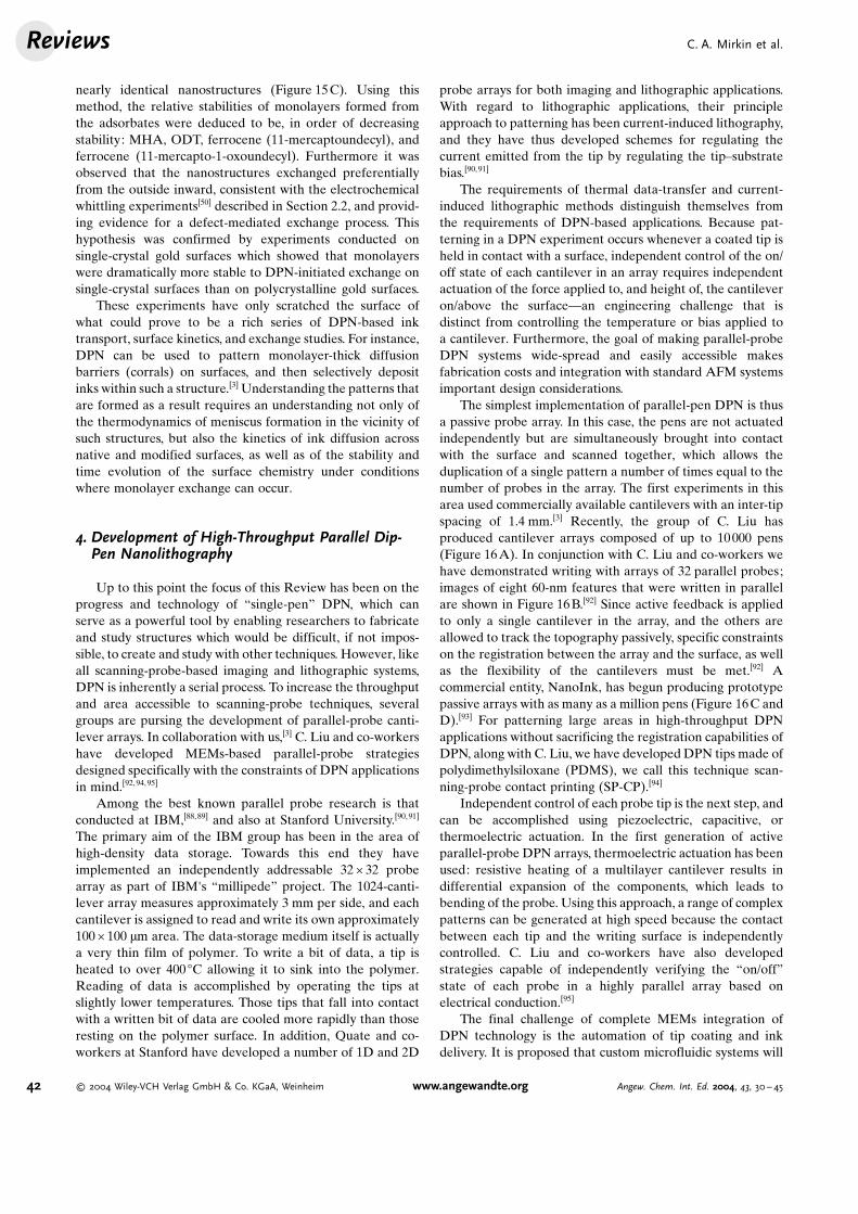
nearly identical nanostructures (Figure 15C). Using thismethod, the relative stabilities of monolayers formed fromthe adsorbates were deduced to be, in order of decreasingstability: MHA, ODT, ferrocene (11-mercaptoundecyl), andferrocene (11-mercapto-1-oxoundecyl). Furthermore it wasobserved that the nanostructures exchanged preferentiallyfrom the outside inward, consistent with the electrochemicalwhittling experiments[50] described in Section 2.2, and provid-ing evidence for a defect-mediated exchange process. Thishypothesis was confirmed by experiments conducted onsingle-crystal gold surfaces which showed that monolayerswere dramatically more stable to DPN-initiated exchange onsingle-crystal surfaces than on polycrystalline gold surfaces.These experiments have only scratched the surface of
what could prove to be a rich series of DPN-based inktransport, surface kinetics, and exchange studies. For instance,DPN can be used to pattern monolayer-thick diffusionbarriers (corrals) on surfaces, and then selectively depositinks within such a structure.[3] Understanding the patterns thatare formed as a result requires an understanding not only ofthe thermodynamics of meniscus formation in the vicinity ofsuch structures, but also the kinetics of ink diffusion acrossnative and modified surfaces, as well as of the stability andtime evolution of the surface chemistry under conditionswhere monolayer exchange can occur.
4. Development of High-Throughput Parallel Dip-Pen Nanolithography
Up to this point the focus of this Review has been on theprogress and technology of “single-pen” DPN, which canserve as a powerful tool by enabling researchers to fabricateand study structures which would be difficult, if not impos-sible, to create and study with other techniques. However, likeall scanning-probe-based imaging and lithographic systems,DPN is inherently a serial process. To increase the throughputand area accessible to scanning-probe techniques, severalgroups are pursing the development of parallel-probe canti-lever arrays. In collaboration with us,[3] C. Liu and co-workershave developed MEMs-based parallel-probe strategiesdesigned specifically with the constraints of DPN applicationsin mind.[92, 94,95]
Among the best known parallel probe research is thatconducted at IBM,[88,89] and also at Stanford University.[90,91]
The primary aim of the IBM group has been in the area ofhigh-density data storage. Towards this end they haveimplemented an independently addressable 32 C 32 probearray as part of IBM's “millipede” project. The 1024-canti-lever array measures approximately 3 mm per side, and eachcantilever is assigned to read and write its own approximately100C 100 mm area. The data-storage medium itself is actuallya very thin film of polymer. To write a bit of data, a tip isheated to over 400 8C allowing it to sink into the polymer.Reading of data is accomplished by operating the tips atslightly lower temperatures. Those tips that fall into contactwith a written bit of data are cooled more rapidly than thoseresting on the polymer surface. In addition, Quate and co-workers at Stanford have developed a number of 1D and 2D
probe arrays for both imaging and lithographic applications.With regard to lithographic applications, their principleapproach to patterning has been current-induced lithography,and they have thus developed schemes for regulating thecurrent emitted from the tip by regulating the tip–substratebias.[90,91]
The requirements of thermal data-transfer and current-induced lithographic methods distinguish themselves fromthe requirements of DPN-based applications. Because pat-terning in a DPN experiment occurs whenever a coated tip isheld in contact with a surface, independent control of the on/off state of each cantilever in an array requires independentactuation of the force applied to, and height of, the cantileveron/above the surface—an engineering challenge that isdistinct from controlling the temperature or bias applied toa cantilever. Furthermore, the goal of making parallel-probeDPN systems wide-spread and easily accessible makesfabrication costs and integration with standard AFM systemsimportant design considerations.The simplest implementation of parallel-pen DPN is thus
a passive probe array. In this case, the pens are not actuatedindependently but are simultaneously brought into contactwith the surface and scanned together, which allows theduplication of a single pattern a number of times equal to thenumber of probes in the array. The first experiments in thisarea used commercially available cantilevers with an inter-tipspacing of 1.4 mm.[3] Recently, the group of C. Liu hasproduced cantilever arrays composed of up to 10000 pens(Figure 16A). In conjunction with C. Liu and co-workers wehave demonstrated writing with arrays of 32 parallel probes;images of eight 60-nm features that were written in parallelare shown in Figure 16B.[92] Since active feedback is appliedto only a single cantilever in the array, and the others areallowed to track the topography passively, specific constraintson the registration between the array and the surface, as wellas the flexibility of the cantilevers must be met.[92] Acommercial entity, NanoInk, has begun producing prototypepassive arrays with as many as a million pens (Figure 16C andD).[93] For patterning large areas in high-throughput DPNapplications without sacrificing the registration capabilities ofDPN, along with C. Liu, we have developedDPN tips made ofpolydimethylsiloxane (PDMS), we call this technique scan-ning-probe contact printing (SP-CP).[94]
Independent control of each probe tip is the next step, andcan be accomplished using piezoelectric, capacitive, orthermoelectric actuation. In the first generation of activeparallel-probe DPN arrays, thermoelectric actuation has beenused: resistive heating of a multilayer cantilever results indifferential expansion of the components, which leads tobending of the probe. Using this approach, a range of complexpatterns can be generated at high speed because the contactbetween each tip and the writing surface is independentlycontrolled. C. Liu and co-workers have also developedstrategies capable of independently verifying the “on/off”state of each probe in a highly parallel array based onelectrical conduction.[95]
The final challenge of complete MEMs integration ofDPN technology is the automation of tip coating and inkdelivery. It is proposed that custom microfluidic systems will
C. A. Mirkin et al.Reviews
42 2004 Wiley-VCH Verlag GmbH & Co. KGaA, Weinheim www.angewandte.org Angew. Chem. Int. Ed. 2004, 43, 30 – 45
ultimately be used to control the inking of individual canti-levers in a parallel probe array. The realization of suchsystems will depend on the development and adaptation of anumber of technologies. Large-scale integration of micro-fluidic technologies is still challenging, and arrays of1000 individually addressable wells represent the currentstate-of-the-art.[96] Thus, to meet the inking needs of parallelprobe arrays (with an ultimate goal of being able to deliver adifferent ink to each probe in a 10000-pen array), newmicrofluidic arrays of addressable ink wells must be imple-mented. Such systems are already under development.[97] Inaddition to microfluidic ink wells into which tips can be“dipped,” integrating the microfluidics directly into the tipsthemselves offers another attractive possibility for MEMsengineers interested in DPN. In an extension of the DPNtechnique that some have likened to a “fountain pen”,[98] bothmicro- and nanopipettes have been used as scanning-probetips with hollow cores through which inks ranging fromchemical etchants[98] to photoresist[99] and even biomole-cules,[26,100] can be pumped directly to a surface for site-specific lithography. Although nanopipette-DPN work ispresently restricted by the hand-fabrication of pulled glasscapillaries, Espinosa and co-workers are lifting this limitationby using advances in microfabrication technology to generatemassively parallel fountain-pen arrays.[101] In this regard, it isstriking to note how the evolution of DPN—from a quill pento a fountain pen to a multiple-pen plotter—has emulated theblueprint provided by the evolution of modern macro-scalewriting and printing technologies. Indeed, this evolution hasfollowed very closely the path proposed at the initialinvention of DPN.[60,102–107]
5. Summary and Outlook
DPN is a unique scanning-probe-based lithographic tool forgenerating high-resolution patternsof chemical functionality on arange of surfaces. The combinationof resolution, registration, anddirect-write capability offered byDPN distinguishes it from anyalternative lithographic strategyand makes DPN a promising toolfor patterning soft organic and bio-logical nanostructures. Many otherrecent lithographic tools that havebeen developed, such as micro-contact patterning (mCP) and nano-imprint lithography (NIL), havebeen driven by the desire tocreate tools that can compete withexisting techniques in the semicon-ductor arena on the basis of costand, in the case of NIL, by offeringhigher resolution. An attractivefeature of DPN is that it is both atool for scientific discovery as wellas an engineering advance thatallows useful multicomponent
nanostructures to be printed at a resolution that is superiorto any conventional lithographic tool. In an age of nano-technology, where being able to fabricate nanostructures of acertain composition, size, and shape is essential, DPN in itscurrent state of development is already a tool that will allowfor rapid advances in the science and technology of highlyminiaturized structures. If the efforts to transform it into amassively parallel process are successful, it will become apowerful production tool in both the life sciences and thesemiconductor industry.This Review has covered several areas of current DPN
research, including the generation of biomolecular nano-arrays for diagnostic applications as well as fundamentalstudies of ligand–receptor interactions. Other particularlyattractive areas of DPN research include the generation oftemplates for assembling (and also for directly depositing)colloidal particles, as well as the creation of a variety of hardnanostructures through direct deposition as well as etching.While much remains to be learned about the DPN depositionprocess, particularly in the area of tip-substrate ink transportand diffusion, several studies published over the past yearhave begun to help clarify things. The transport of twomolecules as similar as ODT and MHA can exhibit differentsensitivities to their environmental conditions, and a completetheory of DPN deposition will need to combine the effects ofmeniscus formation as well as the kinetics of ink transport in amanner that can account for the specific chemistry of anindividual ink. Finally, we have described the ongoingdevelopment of both passive and active parallel-pen DPNarrays. Although predicting the future is troublesome, it isnevertheless fascinating and fun to speculate on the possibil-
Figure 16. Parallel-probe DPN. A) SEM image of a high-density, 2D array of passive DPN probes(courtesy of Chang Liu UIUC) B) Contact-mode AFM topographic images of eight copies of ODT pat-terns generated by using a parallel probe array of AFM cantilevers (reproduced with permission fromref. [92]). C) SEM images of a commercial “Massively Parallel Pen” (MPP) array (courtesy of Nano-Ink, Inc). D) Fluorescence micrograph of spots written with the MPP array (courtesy of NanoInk,Inc.).
Dip-Pen NanolithographyAngewandte
Chemie
43Angew. Chem. Int. Ed. 2004, 43, 30 – 45 www.angewandte.org 2004 Wiley-VCH Verlag GmbH & Co. KGaA, Weinheim
ities that would be opened when such highly parallel DPNsystems are realized. High-throughput deposition of biomo-lecular arrays is one application that comes to mind. Today,scientists use robotic spotting systems (with only 4–16 parallelpins) to generate custom DNA and protein chips. Evenmodestly parallel DPN systems could compete with thesesystems in terms of throughput, thereby allowing the fabri-cation and screening of entire chips using AFM-basedsystems. One could imagine that similar parallel DPN systemscould be applied to combinatorial studies of catalysis, as wellas to the patterning of molecule-based electronic materialswith high levels of registration. Finally, with respect tosemiconductors, the ability to add and remove solid-statematerials from an underlying substrate makes DPN a veryattractive potential tool for lithographic mask fabrication,inspection, and repair. It is clear that DPN has a bright futurein both its single- and multi-pen incarnations.
The Air Force Office of Scientific Research (AFOSR), DefenseAdvanced Research Projects Agency (DARPA), ArmyResearch Office (ARO), and National Science Foundation(NSF) are all acknowledged for support. D.S.G. thanks theNational Institutes of Health (NIH) and DuPont for postdoc-toral fellowship support.
Received: May 22, 2003 [A608]
[1] R. D. Piner, J. Zhu, F. Xu, S. H. Hong, C. A. Mirkin, Science1999, 283, 661.
[2] S. H. Hong, J. Zhu, C. A. Mirkin, Science 1999, 286, 523.[3] S. H. Hong, C. A. Mirkin, Science 2000, 288, 1808.[4] D. A. Weinberger, S. G. Hong, C. A. Mirkin, B. W. Wessels,T. B. Higgins, Adv. Mater. 2000, 12, 1600.
[5] H. Zhang, Z. Li, C. A. Mirkin, Adv. Mater. 2002, 14, 1472.[6] H. Zhang, S.-W. Chung, C. A. Mirkin, Nano Lett. 2003, 3, 43.[7] A. Ivanisevic, K. V. McCumber, C. A. Mirkin, J. Am. Chem.
Soc. 2002, 124, 11997.[8] B. W. Maynor, S. F. Filocamo, M. W. Grinstaff, J. Liu, J. Am.
Chem. Soc. 2002, 124, 522.[9] J. H. Lim, C. A. Mirkin, Adv. Mater. 2002, 14, 1474.[10] A. Noy, A. E. Miller, J. E. Klare, B. L. Weeks, B. W. Woods, J. J.
De Yoreo, Nano Lett. 2002, 2, 109.[11] D. L. Wilson, R. Martin, S. Hong, M. Cronin-Golomb, C. A.
Mirkin, D. L. Kaplan, Proc. Natl. Acad. Sci. USA 2001, 98,13660.
[12] L. M. Demers, D. S. Ginger, S. J. Park, Z. Li, S. W. Chung, C. A.Mirkin, Science 2002, 296, 1836.
[13] M. Ben Ali, T. OndarPuhu, M. Brust, C. Joachim, Langmuir2002, 18, 872.
[14] Y. Li, B. W. Maynor, J. Liu, J. Am. Chem. Soc. 2001, 123, 2105.[15] B. W. Maynor, Y. Li, J. Liu, Langmuir 2001, 17, 2575.[16] L. A. Porter, H. C. Choi, J. M. Schmeltzer, A. E. Ribbe, L. C. C.
Elliott, J. M. Buriak, Nano Lett. 2002, 2, 1369.[17] L. Fu, X. G. Liu, Y. Zhang, V. P. Dravid, C. A. Mirkin, Nano
Lett. 2003, 3, 757.[18] M. Su, X. G. Liu, S. Y. Li, V. P. Dravid, C. A. Mirkin, J. Am.
Chem. Soc. 2002, 124, 1560.[19] J. Hyun, S. J. Ahn, W. K. Lee, A. Chilkoti, S. Zauscher, Nano
Lett. 2002, 2, 1203.[20] N. A. Amro, S. Xu, G.-y. Liu, Langmuir 2000, 16, 3006.[21] P. Manandhar, J. Jang, G. C. Schatz, M. A. Ratner, S. Hong,
Phys. Rev. Lett. 2003, 90, 115505.
[22] B. L. Weeks, A. Noy, A. E. Miller, J. J. De Yoreo, Phys. Rev.Lett. 2002, 88, 255505.
[23] P. E. Sheehan, L. J. Whitman, Phys. Rev. Lett. 2002, 88, 156104.[24] G. Agarwal, L. A. Sowards, R. R. Naik, M. O. Stone, J. Am.
Chem. Soc. 2003, 125, 580.[25] R. McKendry, W. T. S. Huck, B. Weeks, M. Florini, C. Abell, T.
Rayment, Nano Lett. 2002, 2, 713.[26] A. Bruckbauer, L. M. Ying, A. M. Rothery, D. J. Zhou, A. I.
Shevchuk, C. Abell, Y. E. Korchev, D. Klenerman, J. Am.Chem. Soc. 2002, 124, 8810.
[27] S. Matsubara, H. Yamamoto, K. Oshima, E. Mouri, H.Matsuoka, Chem. Lett. 2002, 886.
[28] Y. M. Jung, S. J. Ahn, E. R. Kim, H. Lee, J. Korean Phys. Soc.2002, 40, 712.
[29] X. Hong, L. Wei, W. Guo, J. Li, W. L. Song, Y. B. Bai, T. J. Li,Chem. J. Chin. Univ. 2002, 23, 1778.
[30] L. Wei, X. Hong, W. Guo, Y. B. Bai, T. J. Li, Chem. J. Chin.Univ. 2002, 23, 1386.
[31] J. H. Liao, L. Huang, N. Gu, Chin. Phys. Lett. 2002, 19, 134.[32] H. L. Zhang, Y. Guo, H. L. Li, D. Q. Yang, Chem. J. Chin. Univ.
1999, 20, 1460.[33] S. Rozhok, R. Piner, C. A. Mirkin, J. Phys. Chem. B 2003, 107,
751.[34] K. B. Lee, S. J. Park, C. A. Mirkin, J. C. Smith, M. Mrksich,
Science 2002, 295, 1702.[35] S. P. A. Fodor, Science 1997, 277, 393.[36] E. S. Lander, Nat. Genet. 1999, 21, 3.[37] D. R. Walt, Science 2000, 287, 451.[38] A. Schulze, J. Downward, Nat. Cell Biol. 2001, 3, E190.[39] M. Kato-Maeda, Q. Gao, P. M. Small, Cell. Microbiol. 2001, 3,
713.[40] P. G. Marciano, J. H. Eberwine, R. Raghupathi, T. K. McIntosh,
Restor. Neurol. Neurosci. 2001, 18, 105.[41] F. F. Bier, F. Kleinjung, Fresenius J. Anal. Chem. 2001, 371, 151.[42] D. S. Wilson, S. Nock, Angew. Chem. 2003, 115, 510; Angew.
Chem. Int. Ed. 2003, 42, 494.[43] R. C. Jin, Y. W. Cao, C. A. Mirkin, K. L. Kelly, G. C. Schatz,
J. G. Zheng, Science 2001, 294, 1901.[44] R. Elghanian, J. J. Storhoff, R. C. Mucic, R. L. Letsinger, C. A.
Mirkin, Science 1997, 277, 1078.[45] T. A. Taton, C. A. Mirkin, R. L. Letsinger, Science 2000, 289,
1757.[46] J. H. Lim, D. S. Ginger, K. B. Lee, J. Heo, J. M. Nam, C. A.
Mirkin, Angew. Chem. 2003, 115, 2411; Angew. Chem. Int. Ed.2003, 42, 2309.
[47] K. B. Lee, J. H. Lim, C. A. Mirkin, J. Am. Chem. Soc. 2003, 125,5588.
[48] H. J. Dai, N. Franklin, J. Han, Appl. Phys. Lett. 1998, 73, 1508.[49] G.-Y. Liu, N. A. Amro, Proc. Natl. Acad. Sci. USA 2002, 99,
5165.[50] Y. Zhang, K. Salaita, J. H. Lim, C. A. Mirkin, Nano Lett. 2002,
2, 1389.[51] M. Mrksich, Curr. Opin. Chem. Biol. 2002, 6, 794.[52] J. C. Smith, K.-B. Lee, Q. Wang, M. G. Finn, J. E. Johnson, M.
Mrksich, C. A. Mirkin, Nano Lett. 2003, 3, 883.[53] C. L. Cheung, J. A. Camarero, B. W. Woods, T. W. Lin, J. E.
Johnson, J. J. De Yoreo, J. Am. Chem. Soc. 2003, 125, 6848.[54] Q. Wang, T. W. Lin, J. E. Johnson, M. G. Finn, Chem. Biol.
2002, 9, 813.[55] Q. Wang, E. Kaltgrad, T. W. Lin, J. E. Johnson, M. G. Finn,
Chem. Biol. 2002, 9, 805.[56] L. M. Demers, C. A. Mirkin, Angew. Chem. 2001, 113, 3159;
Angew. Chem. Int. Ed. 2001, 40, 3069.[57] J. P. Hoogenboom, D. L. J. Vossen, C. Faivre-Moskalenko, M.
Dogterom, A. van Blaaderen, Appl. Phys. Lett. 2002, 80, 4828.[58] J. Aizenberg, P. V. Braun, P. Wiltzius, Phys. Rev. Lett. 2000, 84,
2997.
C. A. Mirkin et al.Reviews
44 2004 Wiley-VCH Verlag GmbH & Co. KGaA, Weinheim www.angewandte.org Angew. Chem. Int. Ed. 2004, 43, 30 – 45
[59] A. Ivanisevic, J. H. Im, K. B. Lee, S. J. Park, L. M. Demers, K. J.Watson, C. A. Mirkin, J. Am. Chem. Soc. 2001, 123, 12424.
[60] C. A. Mirkin, MRS Bull. 2000, 25, 43.[61] N. C. Seeman, A. M. Belcher, Proc. Natl. Acad. Sci. USA 2002,
99, 6451.[62] C. M. Niemeyer, Angew. Chem. 2001, 113, 4254; Angew. Chem.
Int. Ed. 2001, 40, 4128.[63] A. P. Alivisatos, K. P. Johnsson, X. G. Peng, T. E. Wilson, C. J.
Loweth, M. P. Bruchez, P. G. Schultz, Nature 1996, 382, 609.[64] L. M. Demers, S. J. Park, T. A. Taton, Z. Li, C. A. Mirkin,
Angew. Chem. 2001, 113, 3161; Angew. Chem. Int. Ed. 2001, 40,3071.
[65] J. C. Garno, Y. Y. Yang, N. A. Amro, S. Cruchon-Dupeyrat,S. W. Chen, G.-Y. Liu, Nano Lett. 2003, 3, 389.
[66] P. T. Hurley, A. E. Ribbe, J. M. Buriak, J. Am. Chem. Soc. 2003,125, 11334.
[67] G. Agarwal, R. R. Naik, M. O. Stone, J. Am. Chem. Soc. 2003,125, 7408.
[68] M. Su, V. P. Dravid, Appl. Phys. Lett. 2002, 80, 4434.[69] G. M. Wallraff, W. D. Hinsberg, Chem. Rev. 1999, 99, 1801.[70] Y. N. Xia, J. A. Rogers, K. E. Paul, G. M. Whitesides, Chem.
Rev. 1999, 99, 1823.[71] Y. Xia, G. M. Whitesides,Angew. Chem. 1998, 110, 568;Angew.
Chem. Int. Ed. 1998, 37, 550.[72] S. Y. Chou, MRS Bull. 2001, 26, 512.[73] M. Albrecht, C. T. Rettner, A. Moser, M. E. Best, B. D. Terris,
Appl. Phys. Lett. 2002, 81, 2875.[74] Y. S. Kim, W. Hong, H. J. Woo, H. W. Choi, G. D. Kim, J. H.
Lee, S. Lee, Jpn. J. Appl. Phys. Part 1 2002, 41, 4141.[75] G. Y. Liu, S. Xu, Y. L. Qian, Acc. Chem. Res. 2000, 33, 457.[76] Y. N. Xia, X. M. Zhao, E. Kim, G. M. Whitesides, Chem. Mater.
1995, 7, 2332.[77] H. Zhang, K.-B. Lee, Z. Li, C. A. Mirkin,Nanotechnology 2003,
14, 1113.[78] M. J. Tarlov, D. R. F. Burgess, G. Gillen, J. Am. Chem. Soc.
1993, 115, 5305.[79] J. Y. Huang, J. C. Hemminger, J. Am. Chem. Soc. 1993, 115,
3342.[80] J. Y. Huang, D. A. Dahlgren, J. C. Hemminger, Langmuir 1994,
10, 626.[81] A. Ivanisevic, C. A. Mirkin, J. Am. Chem. Soc. 2001, 123, 7887.[82] J. K. Jang, S. H. Hong, G. C. Schatz, M. A. Ratner, J. Chem.
Phys. 2001, 115, 2721.[83] J. K. Jang, G. C. Schatz, M. A. Ratner, J. Chem. Phys. 2002, 116,
3875.[84] G. E. Poirier, E. D. Pylant, Science 1996, 272, 1145.[85] G. E. Poirier, M. J. Tarlov, Langmuir 1994, 10, 2853.[86] C. A. Widrig, C. A. Alves, M. D. Porter, J. Am. Chem. Soc.
1991, 113, 2805.[87] S. H. Hong, J. Zhu, C. A. Mirkin, Langmuir 1999, 15, 7897.
[88] P. Vettiger, M. Despont, U. Drechsler, U. Durig, W. Haberle,M. I. Lutwyche, H. E. Rothuizen, R. Stutz, R. Widmer, G. K.Binnig, IBM J. Res. Dev. 2000, 44, 323.
[89] W. P. King, T. W. Kenny, K. E. Goodson, G. L. W. Cross, M.Despont, U. T. Durig, H. Rothuizen, G. Binnig, P. Vettiger, J.Microelectromech. Syst. 2002, 11, 765.
[90] E. M. Chow, G. G. Yaralioglu, C. F. Quate, T. W. Kenny, Appl.Phys. Lett. 2002, 80, 664.
[91] T. Sulchek, R. J. Grow, G. G. Yaralioglu, S. C. Minne, C. F.Quate, S. R. Manalis, A. Kiraz, A. Aydine, A. Atalar, Appl.Phys. Lett. 2001, 78, 1787.
[92] M. Zhang, D. Bullen, S. W. Chung, S. Hong, K. S. Ryu, Z. F.Fan, C. A. Mirkin, C. Liu, Nanotechnology 2002, 13, 212.
[93] L. M. Demers, G. della Cioppa, Genet. Eng. News 2003, 23, 32.[94] X. Wang, K. S. Ryu, D. A. Bullen, J. Zou, H. Zhang, C. A.
Mirkin, C. Liu, Langmuir 2003, 19, 8951.[95] J. Zou, D. Bullen, X. F. Wang, C. Liu, C. A. Mirkin,Appl. Phys.
Lett. 2003, 83, 581.[96] T. Thorsen, S. J. Maerkl, S. R. Quake, Science 2002, 298, 580.[97] D. Banerjee, J. Fragala, T. Duenas, R. Shile, B. Rosner in
Proceedings of the Seventh International Symposium on Mini-aturized Chemical and Biochemical Analysis (micro-TAS 2003)(Squaw Valley, October 5 – 9, 2003), 2003, 1, 58.
[98] A. Lewis, Y. Kheifetz, E. Shambrodt, A. Radko, E. Khatch-atryan, C. Sukenik, Appl. Phys. Lett. 1999, 75, 2689.
[99] M. H. Hong, K. H. Kim, J. Bae, W. Jhe, Appl. Phys. Lett. 2000,77, 2604.
[100] A. Bruckbauer, D. J. Zhou, L. M. Ying, Y. E. Korchev, C. Abell,D. Klenerman, J. Am. Chem. Soc. 2003, 125, 9834.
[101] K.-H. Kim, C. Ke, N. Moldovan, H. D. Espinosa in Proceedingsof the Society of Experimental Mechanics Annual Conference(Charlotte, NC, 2.–4. June 2003), 2003, 235.
[102] C. A. Mirkin, Inorg. Chem. 2000, 39, 2258.[103] C. A. Mirkin, R. D. Piner, S. Hong, U.S. Patent App. No.
20020063212, May 24, 2001.[104] C. A. Mirkin, S. Hong, V. P. Dravid, U.S. Patent App. No.
20020122873, Jan. 28, 2002.[105] C. A. Mirkin, G. della Cioppa, L. Demers, K.-B. Lee, S.-J. Park,
U.S. Patent App. No. 20030068446, Oct. 2, 2002.[106] C. A. Mirkin, V. P. Dravid, M. Su, X. Liu, U.S. Patent App. No.
20030162004, Dec. 17, 2002.[107] C. A. Mirkin, R. Piner, S. Hong, U.S. Patent App. No.
20030157254, Nov. 22, 2002.[108] X. G. Liu, S. W. Liu, C. A. Mirkin, Angew. Chem. 2003, 115,
4785; Angew. Chem. Int. Ed. 2003, 42, 4933.[109] H. Jung, R. Kulkarni, C. P. Collier, J. Am. Chem. Soc. 2003, 125,
12096.[110] X. G. Liu, L. Fu, S. H. Hong, V. P. Dravid, C. A. Mirkin, Adv.
Mater. 2002, 14, 231.[111] D. J. Pena, M. P. Raphael, J. M. Byers, Langmuir 2003, 19, 9028.[112] M. Su, S. Y. Li, V. P. Dravid, J. Am. Chem. Soc. 2003, 125, 9930.
Dip-Pen NanolithographyAngewandte
Chemie
45Angew. Chem. Int. Ed. 2004, 43, 30 – 45 www.angewandte.org 2004 Wiley-VCH Verlag GmbH & Co. KGaA, Weinheim