Embed Size (px)
Citation preview
8/13/2019 2003 Capacitor Mismatch Insensitive 12b Algorithmic Adc
http://slidepdf.com/reader/full/2003-capacitor-mismatch-insensitive-12b-algorithmic-adc 1/4
8/13/2019 2003 Capacitor Mismatch Insensitive 12b Algorithmic Adc
http://slidepdf.com/reader/full/2003-capacitor-mismatch-insensitive-12b-algorithmic-adc 2/4
age is added to the output witho ut the need fo r charge transfer.
B. Amlog Addirion
A concept is presented for implementing he arithmeticopera-
tions ( I ) of the algorithmic ADC in analog hardware without
multiplication. Analog multiplicatio n,within the context of a SCcircuit, is a series of voltage-to-charge and charge-to-voltage
conversions- known also as the charge wnsf er technique QT).
Typical methods for creation of the MX2 are shown in
Fig 2(a),(b). Voltage multiplication by 2 occurs in Fig 2(a)
(C+ZC)[Zlwi th thecharge t ransferof Q = V,.ZCofcapac-
itor C, = 2 C to a another capacitor C, = C. initially dis-
charged. via a vinual earth node to become 2 V,. This method is
sensitive to the ratio of capacitors C,/ C, . An adaptation of this
method is shown in Fig 2(b), which is called a charge transfer
with flip-around C 0 I31, where both C , = C and C, = C
are pre-charged with V,, whereaf ter the charge on C, is m s -
f e d o C,. Half a bit of extra accuracy can be achieved with
the C --f C circuit compared to C 2 C circuit but in practical
applications no better than Is bi ts accura te multiplication-by-2
is realistic using these metho ds in standard CMO S [3]. The 1.5-
bit DAC voltage is added to the output but incurs a multiplica-
tion by 1 ( C / C ) through charge transfer via the virmal earth
node to the output capacitor C,
An alterna tive concep t, C + C, based on voltage addition, is
demonstrated in Fig 2(c). Capacitors can be used for addition,
where instead of multiply ing V by 2, voltage addition occu n by
fin harging each of C, and C, to V, and then placing these
capacitors end to end, with s ay the plate (3) of C, connected to
plate 2) of C ,. To fulfill the 1.5-bit DAC function. the output
can be easily level shifted by adding a voltage at plate (1) of C,.
Due to the pre sence of parasitic cou pling capacitanc e at both
terminals of C ,, C,, when realiz ed in a CMOS process, the
accurate implementation of the C C concept has remained
elusive[I]p t i l l now.
Directimplementation.
as n Fig 2 ( c ) , isonly suita ble for low resolutionADCs of less than 8-bits.
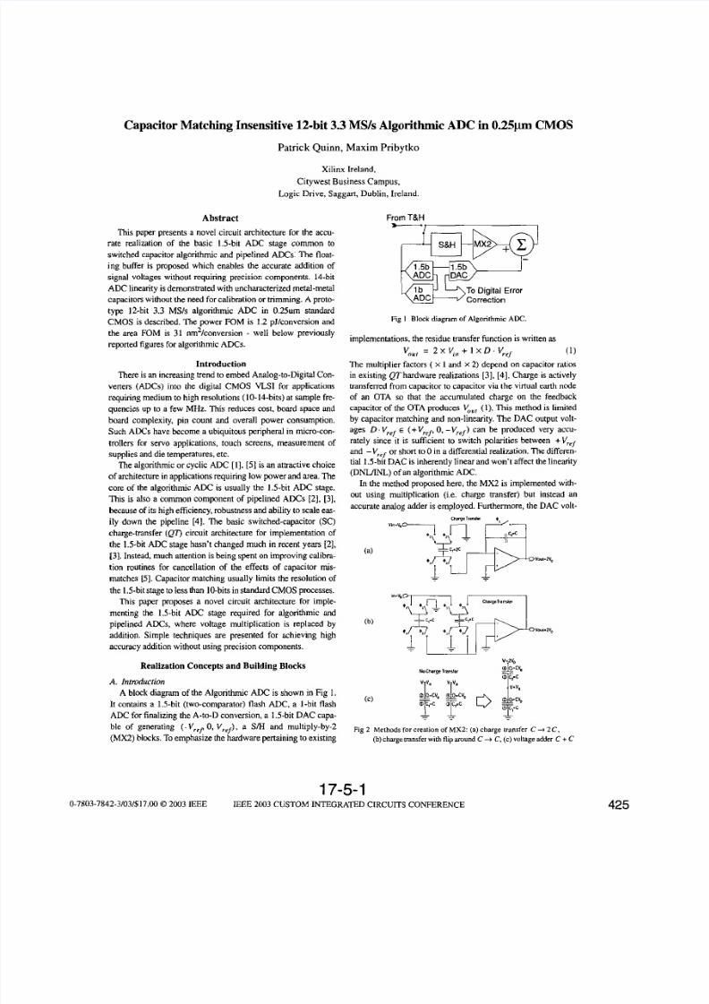
C. Floating Hold Buffer or Accurate Voltage Addition
In order to accurately implem ent the voltage addition concept
of Fig 2(c). a circuit component is proposed with o ne input and
one output, where the output is offset against the input by a dif-
ference voltage VdjIJ with QjlJ being held independent of the
level of the input voltage.
Voltage Vdfn can be sampled and held using a capacitor C .Fig 3 (a),(b). To pr eserve this v oltage, it is sufficient to preserve
charge Q = C . V,lifl on either plate of C. usually the top plate
connected to a high impedance node. Assume that Cis used as a
floating hold capacitor and that the only disch arge pa h from its
top plate terminal is through parasitic capacito r Cpor Fi g 3(c).
Fig 3 a) Sampling capacitor during sampls phase. (b) rampling
capacitor within hold CiruitTy. and (c) ils connection to high
impedance input of =live element during hold p hase.
The voltage across Cis then given by
where VCM= VA is a floating voltage at node A. According to
2). c; depends on V This limits the quality of the floating
voltage hold circuit employing a s ingle samplin g capacitor C.Consider now two such capacitors C C2 precharged to
V,,,, Vrn2- see Fig 4(a). Define the difference voltage as
Vdm = V and assume each of the capacitor top platesis at the Same voltage, i e VI = V = V,, . T h c hold voltage
across bath capacitors of Fig 4(b), V r d = Vc - Vc2. is then
given by
If(C,,,,,,/C, - Cpa,2/C2) (( C,,,,/C, ( 3 ) . 2). then hold volt-age (3) is significantly e s s sensitive to V as compared to (2).
Recall that VI = V ,and the only path for the top plate charge to
escape is through the par asitics. This implies that nodes I ) and
(2) must be physically disconnected.
Fig 4(c) shows the implementation of the floating hold cir-
cuiuy employing C,, C, and a single-ended OTA. The OTA
equalizes the voltages at the top plates of C, and C, by means
of the negative feedback Imp through C, , thus satisfying
VI = V of (3). V .n drives the bottom plate of C, causing a cor-
responding change in node voltage 2) al the OTA positive
input. The voltage difference held across C, and C, is praai-
cally independent of V,, .
This high accuracy floating hold buffer operates such that the
output is unity gain buffered from the in put while m aintaining a
fixed predetermined voltage between output and input. This is
the fundamental building block needed for voltag e addition.
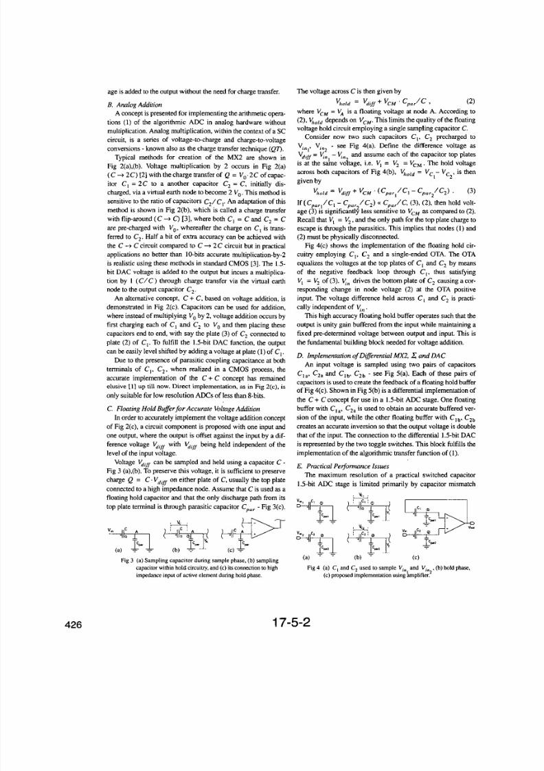
D. ImplemenrotionofDzferenrinl MX2, Z and DAC
An input voltage is sampled using two pain of capacitors
C,,, C,, and C,b,C,, - see Fig 5(a). Each of these pain of
capacitors is used to create the fe edback of a floating hold buffer
of Fig 4(c). Shown in Fig 5(b) is a differential implementation of
the C C concept for use in a 1.5-bit ADC stage. One floating
buffer with C,,, C,, is used to obtain an accurate buffered ver-
sion of the in put, while the other floatin g buffer with C,,, C,,
creates an accurate inversion so that the output voltage is double
that of the input. The c onnectio n to the differential 1.5-bit DAC
is represented by th e two toggle switc hes. This block fulfills the
implementation of the algorithm ic transfer function of I ) .
E. Pracrical Performance Issues
The maximum resolution of a practical switched capacitor
1.5-bit ADC stage is limited primarily by capacitor mismatch
yield = 'dfJ CM cpnr/c 2 (2)
- V' I
V,rold = vd Jfc 'CM (cpo,l/cl cpar2/c2) ( 3 )
Y
_ _
(a) (b) (C)
Fig 4 a) C , and C2 used to sample V, , and V,, , b) hold phase,
(c) pmposed implementation using &m pliii a.*
426 17-5-2
8/13/2019 2003 Capacitor Mismatch Insensitive 12b Algorithmic Adc
http://slidepdf.com/reader/full/2003-capacitor-mismatch-insensitive-12b-algorithmic-adc 3/4
Fig 5 Proposed C C MXZ. Summer and 1.5-bit DAC leve l shift.
(a) m p l e phase. (b) differential hold phaw
and less so by finite amplifier gain a nd charge feedthrough from
the switches. In comparison to the standard C C method
(Fig 2(b)) and assuming sampling capacitors of average value C,
the C C method is less sensitive to capacitor matching by a
fac tor of C/C,,,. whe re C,", is the average value of the para-
sitic capacitors at each amplifie r input. A va lue of C/C,,, = 35
is achieved in the implemented desig n. This implies an extra 4-5
bits accuracy is possible over previous 1.5-bit conversion s tages.
Since the capacitors determine the eff iciency of the ADC. then it
is possible to create a highly efficient architectureusing the pro-
posed C+ C method giving rise to low power and silicon area.
A furtherbenetit of the C Car chitec ture is that it is very insen-
sitive to sampling capa citor non-linearity and so or instance,
small area gate oxide capa citors can be used. The feedback fac-
tor of the C+ C stage is almost double that of the C C.
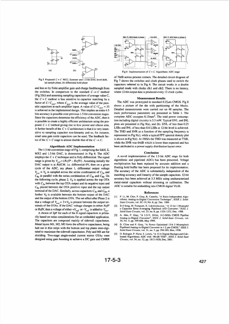
Algor i thmic ADC Implementa t i on
The 1.5-bit conversion stage of Fig I , comprising the S H, 2
MX2 and 1.5-bit DAC. is demonstrated in Fig 6. The ADC
employs the C+ Ctechnique and is fully differential. The signal
range is given by V,<,= (RefP - Re fl) . Assuming initially the
DA C output is at RefCM. i.e. dif fer en tial OV, then on a givencycle of the ADC. say phase I, differe ntial output voltage
V = V, is sampled across the series com binatio n of C3, and
C in parallel with the series com bina tion of C3, a nd C4b.On
the following cycle, phase 2. Vo is applied across the top OTA
with C3, beoveen the top OTA ou tput and its negative input and
C4, placed between the OTA positive input and the top output
terminal of the DAC. Similarly. across capacitors C3, and C4,, a
further Vo is available between the bo ttom output of the D AC
and the output of the bottom OTA. ' h e net effect after Phase 2 is
that a voltage of V,,,= 2 x V0 is present between the output ter-
minals of the OTAs. If the DAC voltage changes to e it he r R e p
or Re p . then a voltage of either V,<, or -V,., is added to V .A choice of 2pF for eac h of the 8 signal capacitors is prima-
rily based on noise considera tions or an em bedded application.
The capacitors are composed mainly of sidewall capacitance.
Metal layers MI, M2, M3 form the effe ctive capacitance, being
laid out in thin strips with the bottom and top plates inter-digi-
t ted to maximize the sidewall capacitance. Poly and M 4 are for
shielding. fio- stag e single-ended current mirror OTAs were
designed using gain bcasting to achieve a DC gain and CMRR
Fig 6 lmplemenfat ion of C + C Algotithmic ADC stage
of 7odB across process com ers. The detailed circuit diagram of
Fig 7 shows the sw itches and clock phases used to switch the
capac itors r e f e d t o in Fig 6. The circuit works in a double
sampled mode with clocks clkl and clw . There is no latency,
where 12-bit output data is produced every 12 clock cycles.
Measurement Resul tsThe AD C was prototyped in standard 0.25pm CM OS. Fig 8
shows a picture of the die with partitioning of the blocks.
Detailed meas urements were carried out on 40 samples. Themain performance parameters are presented in Table 1 The
complete ADC o ccupies 0.1h m. The total power con sum p
tion including digital cir cu iq is5.5 mW. Typical D N L and INL
plots are presented in Fig 9(a), and (b). DNL of less than 0.25
LSBs and INL of less than 0.8 LSBs at 12-bit level is achieved.
The THD and S N R as a function of the sampling freque ncy is
represented in Fig 9( c), while a typical FFT spectral den sity plot
is shown in Fig 9(d). At IMS/s the THDwas measured as 77dB.
while the S N R was 64dB which is lower than expected and has
teen attributedto a power supply distribution layout ermr,
ConclusionA novel implementation of the 1.5-bit ADC stage for both
algoritiunic and pipelined ADCs has been presented. Voltage
multiplication has been replaced by accurate addition and a
floating hold buffer has teen proposed for its implementation.
The accuracy of the D€ s substantially independin1 of the
matching accuracy and linearity of the sample capacitors. 12-bit
accuracy has been a chieved at 3.3 MSIs using uncharacterized
metal-metal capacitors without trimming or calibration. The
ADC is suitable for embedding into CM OS digital VLSI.
References
I l l P. Li. M hin. P. Gray. R. Casrcllo. A Ratio-IndcpendcnLAlgo-rithmic Analog-to-Digital Conversion Technique . IEEE Solid-
Slate Circuirr.vol. SC-19.No. . pp. Dec. 1984.
B-S Sang. M . Tompsetc. K. La krhmi kuma r . A 12-bit I -Msa mpl ds CapaCilOr Error-Averaging Pipelined A D Canvener. lEEE J.
Solid-Store Circuits vol. 23. no. 6, pp. 1324.1332. Dsc. 1988.
A . A b . P. Gray. A 1.5-V. IO-bit. 14.3-MSh CMOS Pipeline
Analog-lo-Digital Convener . IEEE~ J . olid-Stare Circuirr. vol .34. No. 5 pp. 599.606. Ma y 1999.
D. Cline and P. Gray. A Power Optimized 13-b 5 MsamplerlsPipelined Analog-lo-Digiml Convensr in 1.2pm CMOS, IEEEJ
Solid-Smrr Circuirr.vol . 31, no. 3, pp. 294-303. Mar, 1996.
0 Erdogan. P.Hurnt. S.Lewis, A 12-bDigiel-Background-Cali-brated Algorithmic ADC with -90-dB THD. EEE J. Solid Simc
Circui:s.vol.34. no. 12. pp. 1812-1820, Ds W1.
I21
[31
I41
I51
17-5-3 427

8/13/2019 2003 Capacitor Mismatch Insensitive 12b Algorithmic Adc
http://slidepdf.com/reader/full/2003-capacitor-mismatch-insensitive-12b-algorithmic-adc 4/4
dk2
CIW
g 20
.-0 .A
Fig 8 Die photograph showing pani l ianing of blocks,
I 32K FFTplot
I Input frequency 2WkHz
Sampling rate 1.5MWs
Table of Measurements
0 3
0 1024 2046 3072 40
0.6
0.4
0.2
0
-0.2
-0.4
0.6
0.6 0 1024 2048 3012 40
lnpbt frequency 2bOkHi5
80 - f
~ T H D75
70
(C) 65
e 60
50VI
45
40
5
1 2 3 4
0 I 1
Fig 9 Measured A D C Linearity and Dynamic Performance.
428 17-5-4