Embed Size (px)
Citation preview
2002 OSA Annual Meeting - Orlando, Florida
Technical Session WJJ5 - Thin Films II
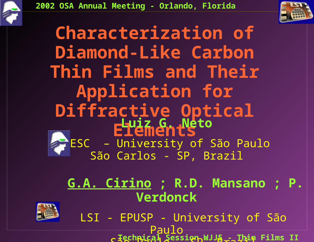
Characterization of Diamond-Like Carbon Thin Films and
Their Application for Diffractive Optical Elements
Luiz G. Neto
EESC – University of São PauloSão Carlos - SP, Brazil
G.A. Cirino ; R.D. Mansano ; P. Verdonck
LSI - EPUSP - University of São Paulo São Paulo - SP, Brazil

2002 OSA Annual Meeting - Orlando, Florida
Technical Session WJJ5 - Thin Films II
Outline
1. Introduction & Goals
2. Results
4. Conclusions
5. Acknowledgments
2002 OSA Annual Meeting - Orlando, Florida
Technical Session WJJ5 - Thin Films II
Introduction
Diffractive Optical Elements (DOE) have a wide range of applications
Amorphous hydrogenated carbon thin films (a:C-H), also called Diamond-Like Carbon (DLC), can be employed as a thin film in several optical applications
2002 OSA Annual Meeting - Orlando, Florida
Technical Session WJJ5 - Thin Films II
Main Goals
Show the applicability of amorphous hydrogenated carbon films (a:C-H) in the micro-optics field, for the fabrication of:
> Diffractive devices:
- Phase-only CGH active - Full complex DOEs material
> Refractive Devices:
- Thin films protective material
(
(
)
)
2002 OSA Annual Meeting - Orlando, Florida
Technical Session WJJ5 - Thin Films II
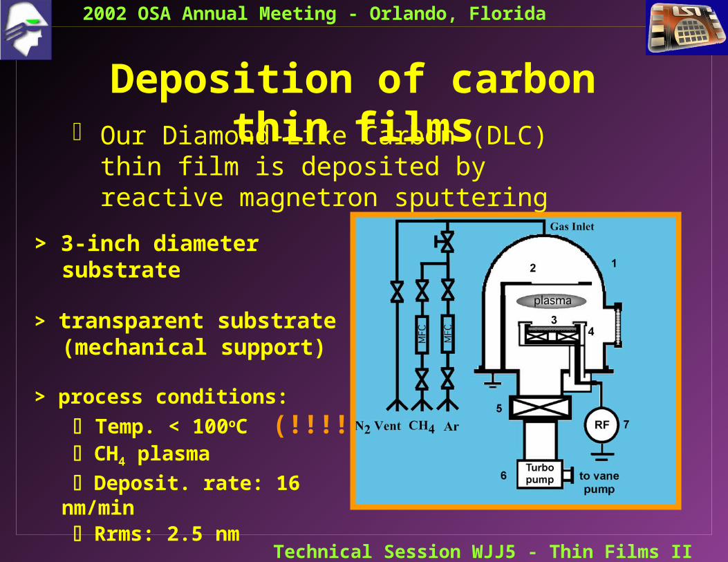
Deposition of carbon thin films Our Diamond-Like Carbon (DLC) thin film is
deposited by reactive magnetron sputtering
> 3-inch diameter substrate
> transparent substrate (mechanical support)
> process conditions:
Temp. < 100oC (!!!!) CH4 plasma
Deposit. rate: 16 nm/min Rrms: 2.5 nm
2002 OSA Annual Meeting - Orlando, Florida
Technical Session WJJ5 - Thin Films II
> Ellipsometry
a priori knowledge of the film thickness is necessary
very good results if silicon substrate is used
> UV / Vis / NIR spectrometry
wavelengths at which film absorption is negligible / nearly complete
Techniques to Characterize DLC Thin Film
2002 OSA Annual Meeting - Orlando, Florida
Technical Session WJJ5 - Thin Films II
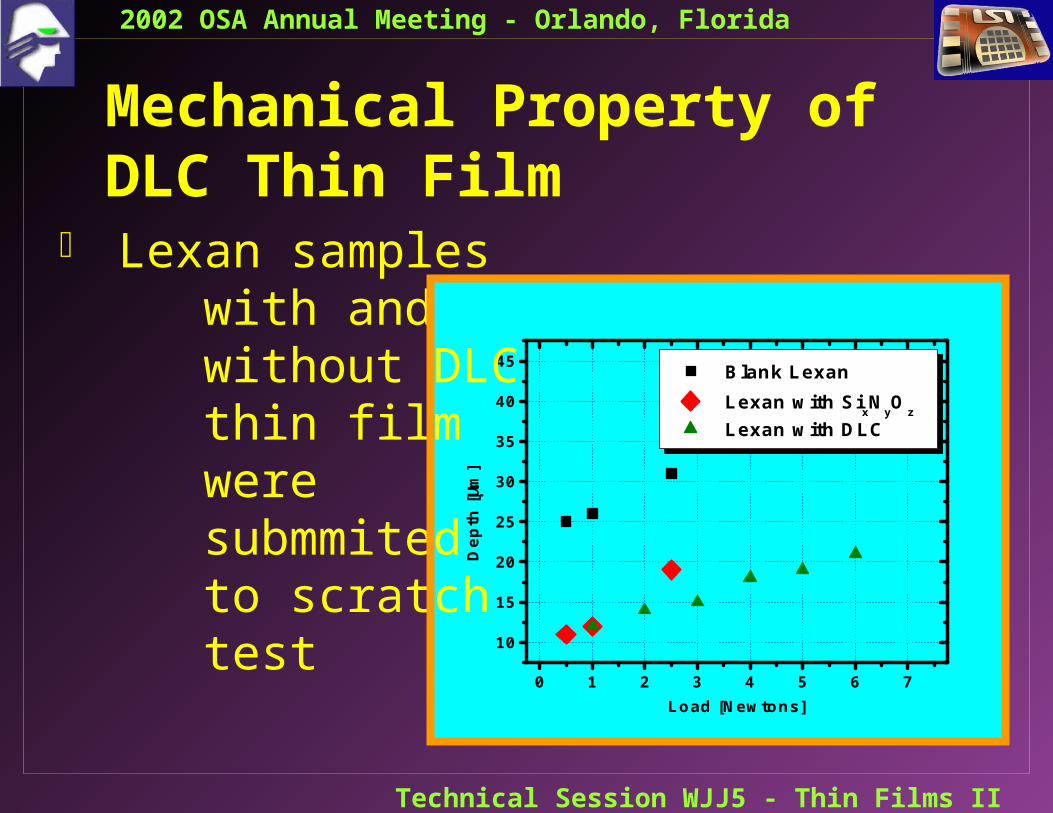
0 1 2 3 4 5 6 7
10
15
20
25
30
35
40
45
Blank Lexan Lexan with Si
xN
yO
z
Lexan with DLC
Dep
th [m
]
Load [Newtons]
Lexan samples with and without DLC thin film were submmited to scratch test
Mechanical Property of DLC Thin Film
2002 OSA Annual Meeting - Orlando, Florida
Technical Session WJJ5 - Thin Films II
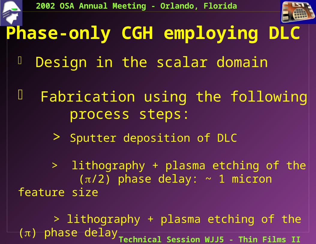
Phase-only CGH employing DLC
Design in the scalar domain
Fabrication using the following process steps:
> Sputter deposition of DLC
> lithography + plasma etching of the (/2) phase delay: ~ 1 micron feature size
> lithography + plasma etching of the () phase delay
2002 OSA Annual Meeting - Orlando, Florida
Technical Session WJJ5 - Thin Films II
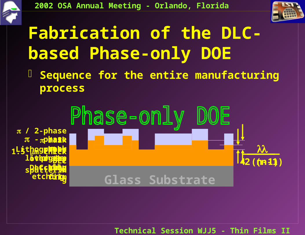
Fabrication of the DLC-based Phase-only DOE Sequence for the entire manufacturing process
Glass Substrate
1.5 m thick DLC
sputtering
/ 2-phasedry
etching
4 (n-1)
- phase mask
lithography - phase
dryetching
2 (n-1)
/ 2-phase maskLithography
over the DLC thin film
2002 OSA Annual Meeting - Orlando, Florida
Technical Session WJJ5 - Thin Films II
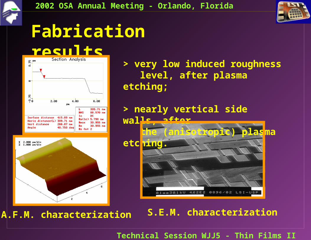
Fabrication results
A.F.M. characterization S.E.M. characterization
> very low induced roughness level, after plasma etching;
> nearly vertical side walls, after the (anisotropic) plasma etching.
2002 OSA Annual Meeting - Orlando, Florida
Technical Session WJJ5 - Thin Films II
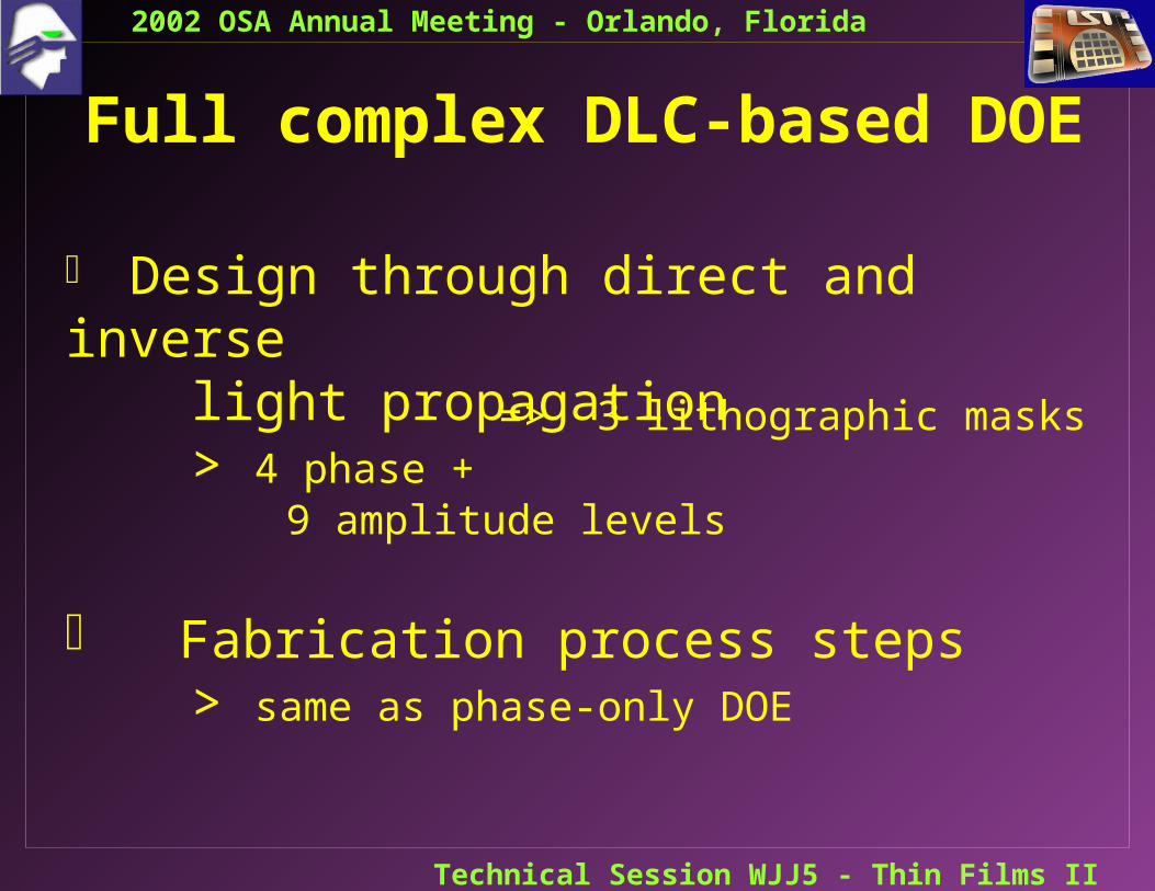
Full complex DLC-based DOE
Design through direct and inverse light propagation > 4 phase + 9 amplitude levels
Fabrication process steps > same as phase-only DOE
=> 3 lithographic masks
2002 OSA Annual Meeting - Orlando, Florida
Technical Session WJJ5 - Thin Films II
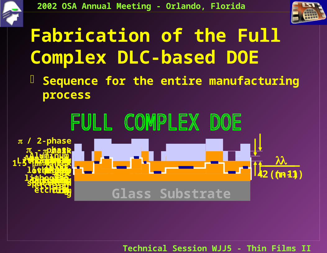
Fabrication of the Full Complex DLC-based DOE Sequence for the entire manufacturing process
Glass Substrate
Aluminumlayer
deposition
1.5 m thick DLC
sputtering
Amplitudemask
lithography
/ 2-phasedry
etching
4 (n-1)
- phase mask
lithography - phase
dryetching
2 (n-1)
/ 2-phase maskLithography
over the DLC thin film
Aluminumlayer
wetetching
2002 OSA Annual Meeting - Orlando, Florida
Technical Session WJJ5 - Thin Films II
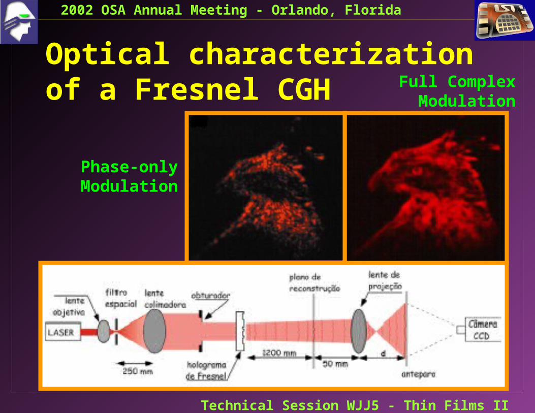
Optical characterizationof a Fresnel CGH Full Complex
Modulation
Phase-onlyModulation
2002 OSA Annual Meeting - Orlando, Florida
Technical Session WJJ5 - Thin Films II
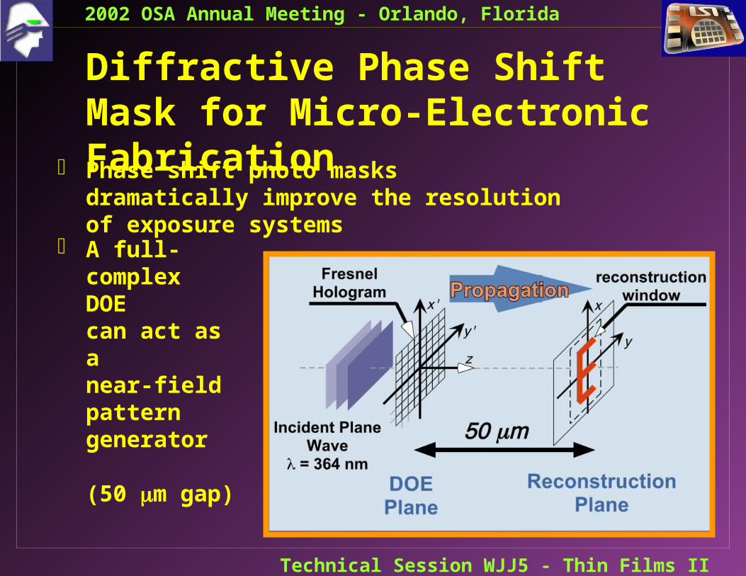
Diffractive Phase Shift Mask for Micro-Electronic Fabrication
Phase shift photo masks dramatically improve the resolution of exposure systems
A full-complexDOE can act as anear-fieldpatterngenerator
(50 m gap)
2002 OSA Annual Meeting - Orlando, Florida
Technical Session WJJ5 - Thin Films II
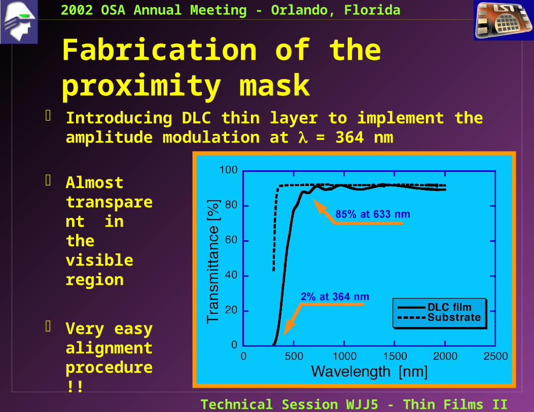
Fabrication of the proximity mask
Introducing DLC thin layer to implement the amplitude modulation at = 364 nm
Almost transparent in the visible region
Very easy alignment procedure !!
2002 OSA Annual Meeting - Orlando, Florida
Technical Session WJJ5 - Thin Films II
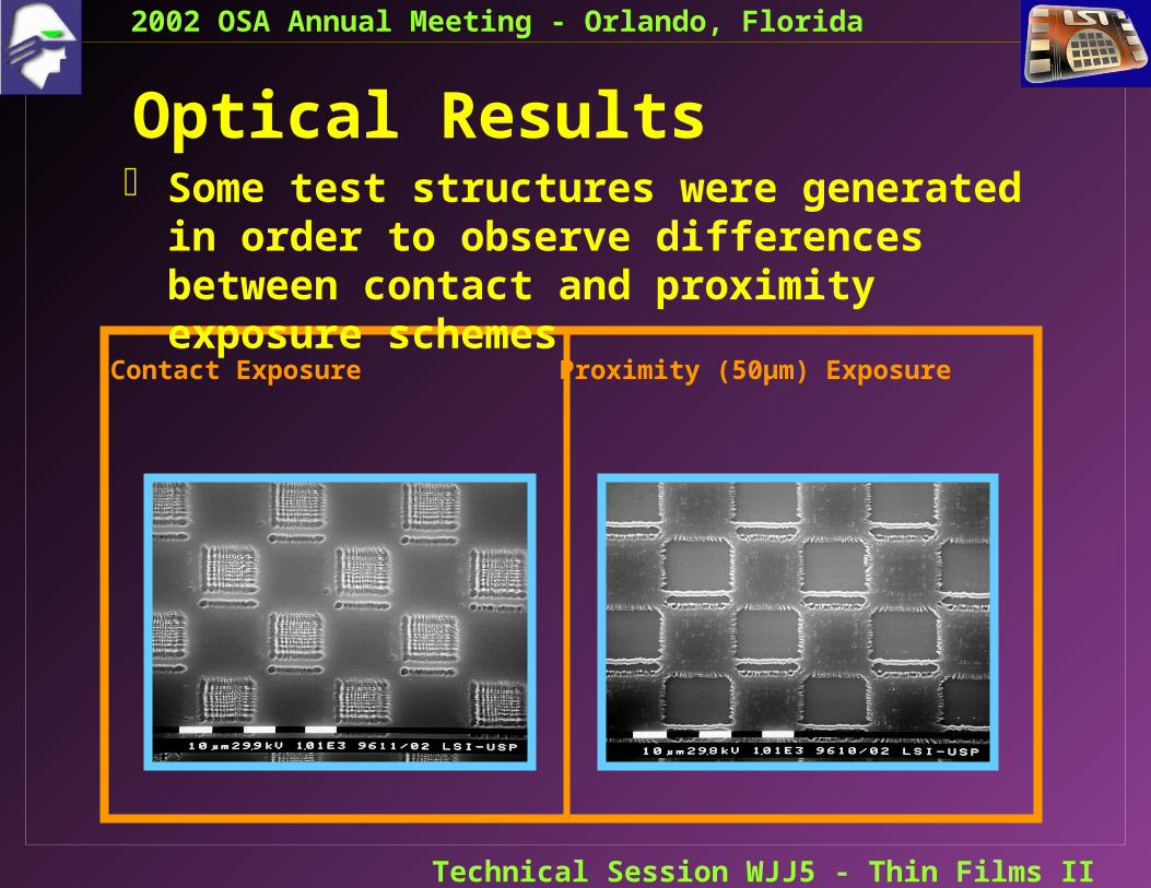
Optical Results
Contact Exposure Proximity (50µm) Exposure
Some test structures were generated in order to observe differences between contact and proximity exposure schemes
2002 OSA Annual Meeting - Orlando, Florida
Technical Session WJJ5 - Thin Films II
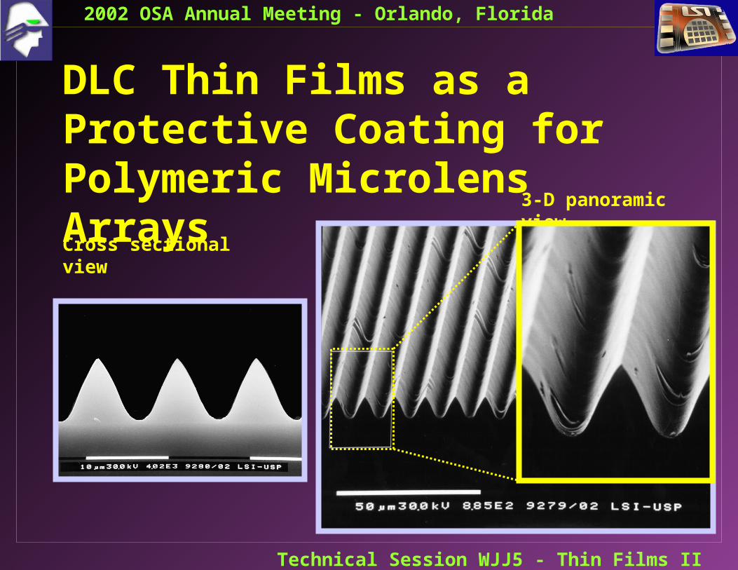
DLC Thin Films as a Protective Coating for Polymeric Microlens Arrays
Cross sectional view
3-D panoramic view
2002 OSA Annual Meeting - Orlando, Florida
Technical Session WJJ5 - Thin Films II
Conclusions DLC thin films are suited to be used as active parts
(and protective coating) of micro-optical devices:
> phase-only modulation CGH, > full complex modulation CGH > full complex modulation phase shift masks > protection layer of polymeric micro-lenses array
Optical characterization of the fabricated devices showed a high quality image with very low speckle noise level
2002 OSA Annual Meeting - Orlando, Florida
Technical Session WJJ5 - Thin Films II
Conclusions (cont)
A full complex-amplitude modulation phase-shift proximity photo mask was designed and fabricated: improvement of the exposure system resolution
A DLC thin layer was introduced to implement the amplitude modulation and a four-phase micro-relief on a fused silica substrate to implement the phase modulation
Optical results showed that diffraction effects are minimized at the mask pattern edges
2002 OSA Annual Meeting - Orlando, Florida
Technical Session WJJ5 - Thin Films II
Acknowledgments
The authors would like to thank the financial support of
> FAPESP,> CenPRA> FINEP and> CNPq.
and
> L. Cescato from UNICAMP, Brazil, for yielding laboratory infra-structure