Embed Size (px)
Citation preview

Confidential Draft9/30/11 CS4361
20-Pin, 24-Bit, 192 kHz, 6-Channel D/A Converter
Features
Multi-Bit Delta-Sigma Modulator
24-Bit Conversion
Automatically Detects Sample Rates Up To 192 kHz
103 dB Dynamic Range
-94 dB THD+N
Low Clock-Jitter Sensitivity
+5 V Core Power
+1.8 V to +5 V Interface Power
Filtered Line-Level Outputs
On-Chip Digital De-emphasis
Popguard® Technology
Mute Output Control
Small 20-pin TSSOP Package
Description
The CS4361 is a complete 6-channel digital-to-analogoutput system including interpolation, multi-bit D/A con-version, and output analog filtering in a small 20-pinpackage. The CS4361 supports all major audio data in-terface formats.
The CS4361 is based on a fourth-order, multi-bit, delta-sigma modulator with a linear analog low-pass filter.This device also includes auto-speed mode detectionusing both sample rate and master clock ratio as amethod of auto-selecting sampling rates between 2 kHzand 216 kHz.
The CS4361 contains on-chip digital de-emphasis, op-erates from a single +5 V power supply with separatebuilt-in level shifter for the digital interface, and requiresminimal support circuitry. These features are ideal forDVD players and recorders, digital televisions, hometheater and set-top box products, and automotive audiosystems.
The CS4361 is available in a 20-pin TSSOP Commer-cial grade package (-40 to 85° C). The CDB4361 is alsoavailable for device evaluation and implementation sug-gestions. Please refer to “Ordering Information” onpage 23 for complete ordering information.
Internal Voltage Reference
+5 Volt-tolerant Reset
Auto-Speed Detecting PCM Serial Interface
Leve
l Tra
nsla
tor
Mode Control
Analog & Digital Core Supply (5 V)
Single-EndedOutputs
(Six Channels6PCM Serial
Audio Input
DigitalFilters
Switch-Cap DAC and
Analog Filters
Multi-bit Modulators
External Mute Control Mute Control
Serial Audio Port & Control Supply (1.8 V to 5 V)
6
Digital De-emphasis
Copyright Cirrus Logic, Inc. 2011(All Rights Reserved)http://www.cirrus.com
SEPT '11DS672F2

CS4361
Confidential Draft9/30/11
TABLE OF CONTENTS1. PIN DESCRIPTIONS .............................................................................................................................. 42. CHARACTERISTICS AND SPECIFICATIONS ...................................................................................... 5
RECOMMENDED OPERATING CONDITIONS .................................................................................... 5ABSOLUTE MAXIMUM RATINGS ........................................................................................................ 5DAC ANALOG CHARACTERISTICS - COMMERCIAL (-CZZ) ............................................................. 6COMBINED INTERPOLATION & ON-CHIP ANALOG FILTER RESPONSE ........................................ 7DIGITAL INPUT CHARACTERISTICS .................................................................................................. 8POWER & THERMAL CHARACTERISTICS ......................................................................................... 8SWITCHING CHARACTERISTICS - SERIAL AUDIO INTERFACE ...................................................... 9
3. TYPICAL CONNECTION DIAGRAM ................................................................................................... 114. APPLICATIONS ................................................................................................................................... 12
4.1 Master Clock .................................................................................................................................. 124.2 Serial Clock .................................................................................................................................... 12
4.2.1 External Serial Clock Mode ................................................................................................... 124.2.2 Internal Serial Clock Mode .................................................................................................... 12
4.3 De-Emphasis ................................................................................................................................. 144.4 Mode Select ................................................................................................................................... 144.5 Initialization and Power-Down ........................................................................................................ 154.6 Output Transient Control ................................................................................................................ 16
4.6.1 Power-Up .............................................................................................................................. 164.6.2 Power-Down .......................................................................................................................... 16
4.7 Grounding and Power Supply Decoupling ..................................................................................... 164.8 Analog Output and Filtering ........................................................................................................... 164.9 Mute Control .................................................................................................................................. 17
5. PERFORMANCE PLOTS ..................................................................................................................... 186. PARAMETER DEFINITIONS ................................................................................................................ 217. PACKAGE INFORMATION .................................................................................................................. 228. ORDERING INFORMATION ................................................................................................................ 239. REVISION HISTORY ............................................................................................................................ 24
2

CS4361
Confidential Draft9/30/11
LIST OF FIGURESFigure 1.Equivalent Output Test Load ........................................................................................................ 8Figure 2.Maximum Loading ......................................................................................................................... 8Figure 3.External Serial Mode Input Timing .............................................................................................. 10Figure 4.Internal Serial Mode Input Timing ............................................................................................... 10Figure 5. Internal Serial Clock Generation ................................................................................................ 10Figure 6.Recommended Connection Diagram .......................................................................................... 11Figure 7.CS4361 Data Format (I²S) .......................................................................................................... 13Figure 8.CS4361 Data Format (Left-Justified) .......................................................................................... 13Figure 9.CS4361 Data Format (Right-Justified 24) ................................................................................... 13Figure 10.CS4361 Data Format (Right-Justified 16) ................................................................................. 14Figure 11.De-Emphasis Curve (Fs = 44.1kHz) ......................................................................................... 14Figure 12.CS4361 Initialization and Power-Down Sequence ................................................................... 15Figure 13.Suggested Active-Low Mute Circuit .......................................................................................... 17Figure 14.Single-Speed Stopband Rejection ............................................................................................ 18Figure 15.Single-Speed Transition Band .................................................................................................. 18Figure 16.Single-Speed Transition Band .................................................................................................. 18Figure 17.Single-Speed Passband Ripple ................................................................................................ 18Figure 18.Double-Speed Stopband Rejection ........................................................................................... 19Figure 19.Double-Speed Transition Band ................................................................................................. 19Figure 20.Double-Speed Transition Band ................................................................................................. 19Figure 21.Double-Speed Passband Ripple ............................................................................................... 19Figure 22.Quad-Speed Stopband Rejection ............................................................................................. 20Figure 23.Quad-Speed Transition Band ................................................................................................... 20Figure 24.Quad-Speed Transition Band ................................................................................................... 20Figure 25.Quad-Speed Passband Ripple ................................................................................................. 20
LIST OF TABLESTable 1. Common Clock Frequencies ....................................................................................................... 12Table 2. Mode Pin Settings ....................................................................................................................... 14
3

CS4361
Confidential Draft9/30/11
1. PIN DESCRIPTIONS
Pin Name # Pin Description
SDIN1SDIN2SDIN3
234
Serial Audio Data Input (Input) - Input for two’s complement serial audio data.
DEM/SCLK 5De-emphasis/External Serial Clock Input (Input) - used for de-emphasis filter control or external serial clock input.
LRCK 6Left Right Clock (Input) - Determines which channel, Left or Right, is currently active on the serial audio data line.
MCLK 7 Master Clock (Input) - Clock source for the delta-sigma modulator and digital filters.
VQ 11 Quiescent Voltage (Output) - Filter connection for internal quiescent voltage.
FILT+ 10Positive Voltage Reference (Output) - Positive reference voltage for the internal sampling circuits.
AOUT1AOUT2AOUT3AOUT4AOUT5AOUT6
191817161312
Analog Output (Output) - The full scale analog output level is specified in the Analog Characteristics specification table.
GND 14 Ground (Input) - ground reference.
VA 15 Analog Power (Input) - Positive power for the analog and core digital sections.
VL 1 Interface Power (Input) - Positive power for the digital interface level shifters.
RST 8 Reset (Input) - Applies reset to the internal circuitry when low.
MUTEC 20 Mute Control (Output) - Control signal for optional external muting circuitry.
MODE 9 Mode Control (Input) - Selects operational modes (see Table 2).
1
2
3
4
5 16
6
7
8
151413
12
11
9
10
17
18
19
20 MUTECVL
AOUT1SDIN1
AOUT2SDIN2
AOUT3SDIN3
AOUT4DEM/SCLK
VALRCK
GNDMCLK
AOUT5RST
AOUT6MODE
VQFILT+
4

CS4361
Confidential Draft9/30/11
2. CHARACTERISTICS AND SPECIFICATIONS
RECOMMENDED OPERATING CONDITIONSAGND = 0 V; all voltages with respect to ground.
ABSOLUTE MAXIMUM RATINGSAGND = 0 V; all voltages with respect to ground.
WARNING: Operation at or beyond these limits may result in permanent damage to the device. Normal operationis not guaranteed at these extremes.
Parameters Symbol Min Nom Max Units
DC Power SupplyVAVL
4.751.7
5.03.3
5.255.25
VV
Specified Temperature Range Commercial TA -40 - +85 C
Parameters Symbol Min Max Units
DC Power SupplyVAVL
-0.3-0.3
6.0VA
VV
Input Current, Any Pin Except Supplies Iin - ±10 mA
Digital Input Voltage (pin 8, RST) VIND -0.3 VA+0.4 V
Digital Input Voltage (all other digital pins) VIND -0.3 VL+0.4 V
Ambient Operating Temperature (power applied) Top -55 125 °C
Storage Temperature Tstg -65 150 °C
5

CS4361
Confidential Draft9/30/11
DAC ANALOG CHARACTERISTICS - COMMERCIALTest Conditions (unless otherwise specified). VA = 5.0 V, VL = 3.3 V, and TA = 25° C. Full-scale input sine wave. Measurement Bandwidth is 10 Hz to 20 kHz. See (Note 1). Specifications apply to all channels unless otherwise indicated.
Notes:
1. One LSB of triangular PDF dither added to data.
Parameter Min Typ Max Unit
Dynamic Performance
Dynamic Range 18 to 24-Bit A-weightedunweighted
16-Bit A-weightedunweighted
99969087
1031009693
----
dBdBdBdB
Total Harmonic Distortion + Noise18 to 24-Bit Ch. 1-2, 0 dB
Ch. 3-4, 0 dBCh. 5-6, 0 dB
-20 dB-60 dB
16-Bit Ch. 1-2, 0 dBCh. 3-4, 0 dBCh. 5-6, 0 dB
-20 dB-60 dB
----------
-93-90-94-80-40-92-89-93-73-33
-86-83-87-76-36-85-82-86-67-27
dBdBdBdBdBdBdBdBdBdB
DAC Analog Characteristics - All Modes
Parameter Symbol Min Typ Max
Interchannel Isolation (1 kHz) - 100 - dB
DC Accuracy
Interchannel Gain Mismatch - 0.1 0.25 dB
Gain Drift - 100 - ppm/°C
Analog Output
Full Scale Output Voltage 0.60•VA 0.65•VA 0.70•VA Vpp
Quiescent Voltage VQ - 0.5•VA - VDC
Max DC Current draw from an AOUT pin IOUTmax - 10 - A
Max Current draw from VQ IQmax - 100 - A
Min AC-Load Resistance (see Figure 2) RL - 3 - k
Max Load Capacitance (see Figure 2) CL - 100 - pF
Output Impedance ZOUT - 100 -
6

CS4361
Confidential Draft9/30/11
COMBINED INTERPOLATION & ON-CHIP ANALOG FILTER RESPONSEThe filter characteristics have been normalized to the sample rate (Fs) and can be referenced to the desired sam-ple rate by multiplying the given characteristic by Fs. (See Note 5)
2. Response is clock-dependent and will scale with Fs.
3. For Single-Speed Mode, the measurement bandwidth is 0.5465 Fs to 3 Fs.For Double-Speed Mode, the measurement bandwidth is 0.577 Fs to 1.4 Fs.For Quad-Speed Mode, the measurement bandwidth is 0.7 Fs to 1 Fs.
4. De-emphasis is available only in Single-Speed Mode.
5. Amplitude vs. Frequency plots of this data are available in “Performance Plots” on page 18.
Parameter Symbol Min Typ Max Unit
Single-Speed Mode
Passband (Note 2) to -0.05 dB cornerto -3 dB corner
00
--
.4780
.4996FsFs
Frequency Response 10 Hz to 20 kHz -.01 - +.08 dB
StopBand .5465 - - Fs
StopBand Attenuation (Note 3) 50 - - dB
Group Delay tgd - 10/Fs - s
De-emphasis Error (Note 4) Fs = 44.1 kHz - - +.05/-.25 dB
Double-Speed Mode
Passband (Note 2) to -0.1 dB cornerto -3 dB corner
00
--
.4650
.4982FsFs
Frequency Response 10 Hz to 20 kHz -.05 - +.2 dB
StopBand .5770 - - Fs
StopBand Attenuation (Note 3) 55 - - dB
Group Delay tgd - 5/Fs - s
Quad-Speed Mode
Passband (Note 2) to -0.1 dB cornerto -3 dB corner
00
--
0.3970.476
FsFs
Frequency Response 10 Hz to 20 kHz 0 - +0.00004 dB
StopBand 0.7 - - Fs
StopBand Attenuation (Note 3) 51 - - dB
Group Delay tgd - 2.5/Fs - s
7

CS4361
Confidential Draft9/30/11
DIGITAL INPUT CHARACTERISTICS
6. RST pin has an input threshold relative to VL, but is VA tolerant.
7. Iin for LRCK is ±20 A max.
POWER & THERMAL CHARACTERISTICS
8. Current consumption increases with increasing FS and increasing MCLK. Typ and Max values arebased on highest FS and highest MCLK. Current variance between speed modes is small.
9. Power-Down Mode is defined when all clock and data lines are held static.
10. Valid with the recommended capacitor values on VQ and FILT+ as shown in the typical connection di-agram in Section 4.
Parameters Symbol Min Typ Max Units
High-Level Input Voltage -all input Pins except RST (% of VL) VIH 70% - - V
Low-Level Input Voltage -all input Pins except RST (% of VL) VIL - - 30% V
High-Level Input Voltage -RST pin (Note 6) (% of VL) VIH 90% - - V
Low-Level Input Voltage -RST pin (% of VL) VIL - - 10% V
Input Leakage Current (Note 7) Iin - - ±10 A
Input Capacitance - 8 - pF
Parameters Symbol5 V Nom
UnitsMin Typ Max
Power Supplies
Power Supply Current normal operation(Note 8)
power-down state (Note 9)
IAILIAIL
----
660.130026
901--
mAmAAA
Power Dissipation normal operationpower-down state (Note 9)
--
3311.63
455-
mWmW
Package Thermal Resistance JA - 72 - °C/Watt
Power Supply Rejection Ratio (Note 10) (1 kHz)(60 Hz)
PSRR --
6040
--
dBdB
AOUTx
AGND
3.3 µF
Vout
RL
CL
Figure 1. Equivalent Output Test Load Figure 2. Maximum Loading
100
50
75
25
2.5 5 10 15
Safe OperatingRegion
Ca
pa
citiv
e L
oad
--
C
(p
F)
L
Resistive Load -- R (k )L
125
3
20
8

CS4361
Confidential Draft9/30/11
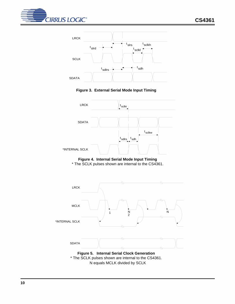
SWITCHING CHARACTERISTICS - SERIAL AUDIO INTERFACE
11. Not all sample rates are supported for all clock ratios. See table “Common Clock Frequencies” onpage 12 for supported ratios and frequencies.
12. In Internal SCLK Mode, the duty cycle must be 50% ±1/2 MCLK period.
13. The SCLK / LRCK ratio may be either 32, 48, 64, or 72. This ratio depends on data format andMCLK/LRCK ratio. (See Figures 7-10)
Parameters Symbol Min Typ Max Units
MCLK Frequency 0.512 - 50 MHz
MCLK Duty Cycle 45 - 55 %
Input Sample Rate All MCLK/LRCK ratios combined(Note 11) 256x, 384x, 1024x
256x, 384x512x, 768x
1152x128x, 192x
64x, 96x128x, 192x
Fs 2284423050
100168
216541346734108216216
kHzkHzkHzkHzkHzkHzkHzkHz
External SCLK Mode
LRCK Duty Cycle (External SCLK only) 45 50 55 %
SCLK Pulse Width Low tsclkl 20 - - ns
SCLK Pulse Width High tsclkh 20 - - ns
SCLK Duty Cycle 45 50 55 %
SCLK rising to LRCK edge delay tslrd 20 - - ns
SCLK rising to LRCK edge setup time tslrs 20 - - ns
SDIN valid to SCLK rising setup time tsdlrs 20 - - ns
SCLK rising to SDIN hold time tsdh 20 - - ns
Internal SCLK Mode
LRCK Duty Cycle (Internal SCLK only) (Note 12) - 50 - %
SCLK Period (Note 13)tsclkw - - ns
SCLK rising to LRCK edgetsclkr - - s
SDIN valid to SCLK rising setup timetsdlrs - - ns
SCLK rising to SDIN hold timeMCLK / LRCK =1152, 1024, 512, 256, 128, or 64
tsdh - - ns
SCLK rising to SDIN hold timeMCLK / LRCK = 768, 384, 192, or 96
tsdh - - ns
109
SCLK----------------
tsclkw2
------------------
109
512 Fs---------------------- 10+
109
512 Fs---------------------- 15+
109
384 Fs---------------------- 15+
9
CS4361
Confidential Draft9/30/11
sclkhtslrst
slrdt
sdlrst sdht
sclklt
SDATA
SCLK
LRCK
Figure 3. External Serial Mode Input Timing
SDATA
*INTERNAL SCLK
LRCK
sclkwt
sdlrst sdht
sclkrt
Figure 4. Internal Serial Mode Input Timing* The SCLK pulses shown are internal to the CS4361.
SDATA
LRCK
MCLK
*INTERNAL SCLK
1 N2
N
Figure 5. Internal Serial Clock Generation* The SCLK pulses shown are internal to the CS4361.
N equals MCLK divided by SCLK
10

CS4361
Confidential Draft9/30/11
3. TYPICAL CONNECTION DIAGRAM
DEM/SCLK
14
AudioData
Processor
External Clock MCLK
GND
CS4361
SDIN1
LRCK
VL
AOUT1
6
2
5
7
10.1 µF
+1 µF
19
Audio Output
+5 V
3.3 µF
10 k C
470
+
R + 470C =
4Fs(R 470)
Rext
ext
ext
+
0.1 µF
33
+
µF
10
VQ
FILT+
11
Note*
Note* = This circuitry is intended for applications where the CS4361 connects directly to an unbalanced output of the design. For internal routing applications please see the DAC analog output characteristics for loading limitations.
For best 20 kHz response
SDIN23
SDIN34
20MUTEC
AOUT2 18
AOUT3 17
AOUT4 16
AOUT5 13
AOUT6 12
Optional Muting Circuit
RST8
Controler
MODE9
+1.8 V to +5 V
VA
15
VL
GND
LRCK
LJ
RJ16
RJ24
I2S
MCLKµF*3.3
µF*10
*Popguard ramp can be adjusted by selecting this capacitor value to be 3.3 µF to give 250 ms ramp time or 10 µF to give a 420 ms ramp time.
or
Figure 6. Recommended Connection Diagram
11

CS4361
Confidential Draft9/30/11
4. APPLICATIONS
The CS4361 accepts data at standard audio sample rates including 48, 44.1 and 32 kHz in SSM, 96, 88.2 and64 kHz in DSM, and 192, 176.4 and 128 kHz in QSM. Audio data is input via the serial data input pin (SDIN). TheLeft/Right Clock (LRCK) determines which channel is currently being input on SDIN, and the optional Serial Clock(SCLK) clocks audio data into the input data buffer.
4.1 Master Clock
MCLK/LRCK must be an integer ratio as shown in Table 1. The LRCK frequency is equal to Fs, the frequen-cy at which words for each channel are input to the device. The MCLK-to-LRCK frequency ratio and speedmode is detected automatically during the initialization sequence by counting the number of MCLK transi-tions during a single LRCK period and by detecting the absolute speed of MCLK. Internal dividers are setto generate the proper clocks. Table 1 illustrates several standard audio sample rates and the requiredMCLK and LRCK frequencies. Please note there is no required phase relationship, but MCLK, LRCK, andSCLK must be synchronous.
Table 1. Common Clock Frequencies
4.2 Serial Clock
The serial clock controls the shifting of data into the input data buffers. The CS4361 supports both externaland internal serial clock generation modes. Refer to Figures 7-10 for data formats.
4.2.1 External Serial Clock Mode
The CS4361 will enter the External Serial Clock Mode when 16 low-to-high transitions are detected onthe DEM/SCLK pin during any phase of the LRCK period. When this mode is enabled, the Internal SerialClock Mode and de-emphasis filter cannot be accessed. The CS4361 will switch to Internal Serial ClockMode if no low-to-high transitions are detected on the DEM/SCLK pin for two consecutive frames ofLRCK. Refer to Figure 12.
4.2.2 Internal Serial Clock Mode
In the Internal Serial Clock Mode, the serial clock is internally derived and synchronous with MCLK andLRCK. The SCLK/LRCK frequency ratio is either 32, 48, 64, or 72 depending upon data format. Operationin this mode is identical to operation with an external serial clock synchronized with LRCK. This mode al-lows access to the digital de-emphasis function. Refer to Figures 7 - 12 for details.
LRCK(kHz)
MCLK (MHz)
64x 96x 128x 192x 256x 384x 512x 768x 1024x 1152x
32 - - - - 8.1920 12.2880 - - 32.7680 36.864044.1 - - - - 11.2896 16.9344 22.5792 33.8680 45.1580 -48 - - - - 12.2880 18.4320 24.5760 36.8640 49.1520 -64 - - 8.1920 12.2880 - - 32.7680 49.1520 - -
88.2 - - 11.2896 16.9344 22.5792 33.8680 - - - -96 - - 12.2880 18.4320 24.5760 36.8640 - - - -
128 8.1920 12.2880 - - 32.7680 49.1520 - - - -176.4 11.2896 16.9344 22.5792 33.8680 - - - - - -192 12.2880 18.4320 24.5760 36.8640 - - - - - -
Mode QSM DSM SSM
12

CS4361
Confidential Draft9/30/11
LRCK
SCLK
Left Channel Right Channel
SDATA +3 +2 +1 LSB+5 +4MSB -1 -2 -3 -4 -5 +3 +2 +1 LSB+5 +4MSB -1 -2 -3 -4
Internal SCLK Mode External SCLK Mode
I²S, 16-Bit data and INT SCLK = 32 Fs ifMCLK/LRCK = 1024, 512, 256, 128, or 64I²S, Up to 24-Bit data and INT SCLK = 48 Fs if MCLK/LRCK = 768, 384, 192, or 96I²S, Up to 24-Bit data and INT SCLK = 72 Fs if MCLK/LRCK = 1152
I²S, up to 24-Bit DataData Valid on Rising Edge of SCLK
Figure 7. CS4361 Data Format (I²S)
LRCK
SCLK
Left Channel Right Channel
SDATA +3 +2 +1 LSB+5 +4MSB -1 -2 -3 -4 -5 +3 +2 +1 LSB+5 +4MSB -1 -2 -3 -4
Internal SCLK Mode External SCLK Mode
Left-Justified, up to 24-Bit DataINT SCLK = 64 Fs if MCLK/LRCK = 1024, 512, 256, 128, or 64INT SCLK = 48 Fs if MCLK/LRCK = 768, 384, 192, or 96INT SCLK = 72 Fs if MCLK/LRCK = 1152
Left-Justified, up to 24-Bit DataData Valid on Rising Edge of SCLK
Figure 8. CS4361 Data Format (Left-Justified)
LRCK
SCLK
Left Channel
SDATA 6 5 4 3 2 1 0723 22 21 20 19 18 6 5 4 3 2 1 0723 22 21 20 19 18
32 clocks
0
Right Channel
Internal SCLK Mode External SCLK Mode
Right-Justified, 24-Bit DataINT SCLK = 64 Fs if MCLK/LRCK = 1024, 512, 256, 128, or 64INT SCLK = 48 Fs if MCLK/LRCK = 768, 384, 192, or 96INT SCLK = 72 Fs if MCLK/LRCK = 1152
Right-Justified, 24-Bit DataData Valid on Rising Edge of SCLKSCLK Must Have at Least 48 Cycles per LRCK Period
Figure 9. CS4361 Data Format (Right-Justified 24)
13

CS4361
Confidential Draft9/30/11
4.3 De-Emphasis
The CS4361 includes on-chip digital de-emphasis. Figure 11 shows the de-emphasis curve for Fs equal to44.1 kHz. The frequency response of the de-emphasis curve will scale proportionally with changes in sam-ple rate, Fs. The de-emphasis filter is active (inactive) if the DEM/SCLK pin is low (high) for five consecutivefalling edges of LRCK. This function is available only in the internal Serial Clock Mode when LRCK < 50 kHz.
4.4 Mode Select
Mode selection is determined by the Mode Select pin. The value of this pin is locked 1024 LRCK cycles afterRST is released. This pin requires a specific connection to supply, ground, MCLK, or LRCK as outlined inTable 2.
Table 2. Mode Pin Settings
Mode pin is: Mode FigureTied to VL I²S 7
Tied to GND Left-Justified 8Tied to LRCK Right-Justified - 24 bit 9Tied to MCLK Right-Justified - 16bit 10
LRCK
SCLK
Left Channel Right Channel
SDATA 6 5 4 3 2 1 09 8 715 14 13 12 11 10 6 5 4 3 2 1 09 8 715 14 13 12 11 10
32 clocksInternal SCLK Mode External SCLK Mode
Right-Justified, 16-Bit DataINT SCLK = 32 Fs if MCLK/LRCK = 1024, 512, 256, 128, or 64INT SCLK = 48 Fs if MCLK/LRCK = 768, 384, 192, or 96INT SCLK = 72 Fs if MCLK/LRCK = 1152
Right-Justified, 16-Bit DataData Valid on Rising Edge of SCLKSCLK Must Have at Least 32 Cycles per LRCK Period
Figure 10. CS4361 Data Format (Right-Justified 16)
GaindB
-10dB
0dB
Frequency
T2 = 15 µs
T1=50 µs
F1 F23.183 kHz 10.61 kHz
Figure 11. De-Emphasis Curve (Fs = 44.1kHz)
14

CS4361
Confidential Draft9/30/11
4.5 Initialization and Power-Down
The initialization and power-down sequence flow chart is shown in Figure 12. The CS4361 enters the pow-er-down state upon initial power-up. The interpolation filters and delta-sigma modulators are reset, and theinternal voltage reference, multi-bit digital-to-analog converters, and switched-capacitor low-pass filters arepowered down. The device will remain in the Power-Down Mode until RST is released and MCLK and LRCKare present. Once MCLK and LRCK are detected, MCLK occurrences are counted over one LRCK periodto determine the MCLK/LRCK frequency ratio. Power is then applied to the internal voltage reference. Final-ly, power is applied to the D/A converters and switched-capacitor filters, and the analog outputs will ramp tothe quiescent voltage, VQ.
USER: Apply Power
Wait State
USER: Apply LRCK and MCLK
MCLK/LRCK Ratio Detection
USER: Applied SCLK
USER: RemoveLRCK
USER: changeMCLK/LRCK ratio
SCLK mode = internal SCLK mode = external
Normal OperationDe-emphasis
available
Analog Outputis Generated
Normal OperationDe-emphasisnot available
Analog Outputis Generated
USER: changeMCLK/LRCK ratio
USER: Apply RSTor remove MCLK
USER: RemoveLRCK
USER: Apply RSTor remove MCLK
USER: Apply MCLK, release RST
Power-Down StateVQ and outputs low
VQ and outputsramp down
VQ and outputsramp down
VQ and outputs ramp up
USER: No SCLK
Figure 12. CS4361 Initialization and Power-Down Sequence
15

CS4361
Confidential Draft9/30/11
4.6 Output Transient Control
The CS4361 uses Popguard technology to minimize the effects of output transients during power-up andpower-down. When implemented with external DC-blocking capacitors connected in series with the audiooutputs, this feature eliminates the audio transients commonly produced by single-ended, single-supplyconverters. To make the best use of this feature, it is necessary to understand its operation.
4.6.1 Power-Up
When the device is initially powered up, the audio outputs, AOUT1-6, are clamped to VQ, which is initiallylow. After RST is released and MCLK is applied, the outputs begin to ramp with VQ towards the nominalquiescent voltage. This ramp takes approximately 200 ms to complete. The gradual voltage ramping al-lows time for the external DC-blocking capacitors to charge to VQ, effectively blocking the quiescent DCvoltage. Audio output begins approximately 2000 sample periods after valid LRCK and SDIN are supplied(and SCLK, if used).
4.6.2 Power-Down
To prevent audio transients at power-down, the DC-blocking capacitors must fully discharge before turn-ing off the power. In order to do this, either stop MCLK or hold RST low for a period of about 250 ms beforeremoving power. During this time, voltage on VQ and the audio outputs discharge gradually to GND. Ifpower is removed before this 250 ms time period has passed, a transient will occur when the VA supplydrops below that of VQ. There is no minimum time for a power cycle; power may be reapplied at any time.
When changing clock ratio or sample rate, it is recommended that zero data (or near zero data) be presenton SDIN for at least 10 LRCK samples before the change is made. During the clocking change, the DACoutputs will always be in a zero data state. If non-zero audio is present at the time of switching, a slightclick or pop may be heard as the DAC output automatically goes to its zero data state.
4.7 Grounding and Power Supply Decoupling
As with any high-resolution converter, the CS4361 requires careful attention to power supply and groundingarrangements to optimize performance. Figure 6 shows the recommended power arrangement, with VAconnected to a clean +5 V supply. For best performance, decoupling and filter capacitors should be locatedas close to the device package as possible, with the smallest capacitors placed closest.
4.8 Analog Output and Filtering
The analog filter present in the CS4361 is a switched-capacitor filter followed by a continuous-time, low-pass filter. Its response, combined with that of the digital interpolator, is given in Figures 14 - 21. The rec-ommended external analog circuitry is shown in the “Typical Connection Diagram” on page 11.
The analog outputs are named AOUT1-6. The SDIN1 feeds AOUT1 as the ‘Left’ marked data and AOUT2as the ‘Right’ marked data. The SDIN2 feeds AOUT3 as the ‘Left’ marked data and AOUT4 as the ‘Right’marked data. The SDIN3 feeds AOUT5 as the ‘Left’ marked data and AOUT6 as the ‘Right’ marked data.
16

CS4361
Confidential Draft9/30/11
4.9 Mute Control
The MUTEC pin is intended to be used as control for an external mute circuit in order to add off-chip mutecapability.
This pin becomes active under the following conditions:
1. During power-up initialization
2. Upon reset
3. If the MCLK to LRCK ratio is incorrect
4. Upon receipt of 512 consecutive samples of zero
5. During power-down
The MUTEC pin will only go active on static zero data only if all 6 channels satisfy the 512 sample require-ment. If any channel receives non-zero data, the mute pin will return low (inactive).
Use of the mute control function is not mandatory but is recommended for designs requiring the absoluteminimum in extraneous clicks and pops. Also, use of the mute control function can enable the system de-signer to achieve idle channel noise and signal-to-noise ratios that are only limited by the external mute cir-cuit. The MUTEC pin is an active-high CMOS driver. See Figure 13 below for a suggested active-high mutecircuit.
470 AudioOut
2 k
10 k
-V
+VA
MMUN2111LT1
AOUT
MUTEC
CS4361
ACCouple
47 k10 k
FilterCap
MMUN2211LT1
(if available)
6
6
(Low Ron)
Figure 13. Suggested Active-Low Mute Circuit
17

CS4361
Confidential Draft9/30/11
5. PERFORMANCE PLOTS
Figure 14. Single-Speed Stopband Rejection Figure 15. Single-Speed Transition Band
Figure 16. Single-Speed Transition Band Figure 17. Single-Speed Passband Ripple
18

CS4361
Confidential Draft9/30/11
Figure 18. Double-Speed Stopband Rejection Figure 19. Double-Speed Transition Band
Figure 20. Double-Speed Transition Band Figure 21. Double-Speed Passband Ripple
19

CS4361
Confidential Draft9/30/11
Figure 22. Quad-Speed Stopband Rejection Figure 23. Quad-Speed Transition Band
0.35 0.4 0.45 0.5 0.55 0.6 0.65 0.7 0.75
-60
-50
-40
-30
-20
-10
0
Am
plitu
de (
dB)
Frequency(normalized to Fs)0 0.1 0.2 0.3 0.4 0.5 0.6 0.7 0.8 0.9 1
-100
-90
-80
-70
-60
-50
-40
-30
-20
-10
0
Am
plitu
de (
dB)
Frequency(normalized to Fs)
0.05 0.1 0.15 0.2 0.25 0.3 0.35 0.4 0.45
-0.2
-0.15
-0.1
-0.05
0
0.05
0.1
0.15
0.2
Am
plitu
de (
dB)
Frequency(normalized to Fs)
Figure 24. Quad-Speed Transition Band Figure 25. Quad-Speed Passband Ripple
0.4 0.45 0.5 0.55 0.6 0.65 0.7
-50
-45
-40
-35
-30
-25
-20
-15
-10
-5
0
Am
plitu
de (
dB)
Frequency(normalized to Fs)
20

CS4361
Confidential Draft9/30/11
6. PARAMETER DEFINITIONS
Total Harmonic Distortion + Noise (THD+N)
The ratio of the rms value of the signal to the rms sum of all other spectral components over the specifiedbandwidth (typically 10 Hz to 20 kHz), including distortion components. Expressed in decibels.
Dynamic Range
The ratio of the full-scale rms value of the signal to the rms sum of all other spectral components over thespecified bandwidth. Dynamic range is a signal-to-noise measurement over the specified bandwidth madewith a -60 dBFS signal. 60 dB is then added to the resulting measurement to refer the measurement to fullscale. This technique ensures that the distortion components are below the noise level and do not effect themeasurement. This measurement technique has been accepted by the Audio Engineering Society, AES17-1991, and the Electronic Industries Association of Japan, EIAJ CP-307.
Interchannel Isolation
A measure of crosstalk between the left and right channels. Measured for each channel at the converter'soutput with all zeros to the input under test and a full-scale signal applied to the other channel. Units in deci-bels.
Interchannel Gain Mismatch
The gain difference between left and right channels. Units in decibels.
Gain Error
The deviation from the nominal full scale analog output for a full scale digital input.
Gain Drift
The change in gain value with temperature. Units in ppm/°C.
21

CS4361
Confidential Draft9/30/11
7. PACKAGE INFORMATION
Notes:
1. “D” and “E1” are reference datums and do not included mold flash or protrusions, but do include moldmismatch and are measured at the parting line, mold flash or protrusions shall not exceed 0.20 mm perside.
2. Dimension “b” does not include dambar protrusion/intrusion. Allowable dambar protrusion shall be0.13 mm total in excess of “b” dimension at maximum material condition. Dambar intrusion shall not re-duce dimension “b” by more than 0.07 mm at least material condition.
3. These dimensions apply to the flat section of the lead between 0.10 and 0.25 mm from lead tips.
INCHES MILLIMETERS NOTE
DIM MIN NOM MAX MIN NOM MAXA -- -- 0.043 -- -- 1.10
A1 0.002 0.004 0.006 0.05 -- 0.15A2 0.03346 0.0354 0.037 0.85 0.90 0.95b 0.00748 0.0096 0.012 0.19 0.245 0.30D 0.252 0.256 0.259 6.40 6.50 6.60 2,3E 0.248 0.2519 0.256 6.30 6.40 6.50 1
E1 0.169 0.1732 0.177 4.30 4.40 4.50e -- -- 0.026 -- -- 0.65 1L 0.020 0.024 0.028 0.50 0.60 0.70µ 0° 4° 8° 0° 4° 8°
JEDEC #: MO-153
Controlling Dimension is Millimeters.
20L TSSOP (4.4 mm BODY) PACKAGE DRAWING
E
N
1 2 3
e b2 A1
A2 A
D
SEATINGPLANE
E11
L
SIDE VIEW
END VIEW
TOP VIEW
22

CS4361
Confidential Draft9/30/11
8. ORDERING INFORMATION
Product Description Package Pb-Free Grade Temp Range Container Order #
CS436120-pin, 24-bit,
192 kHz, 6-channel D/A Converter
20-Plastic TSSOP
Yes Commercial -40 to 85° CTube CS4361-CZZ
Tape and Reel CS4361-CZZR
CDB4361 CS4361 Evaluation Board - - - - CDB4361
23

CS4361
Confidential Draft9/30/11
9. REVISION HISTORY
Release Changes
A1 Initial Release.
A2 Correction to PDF file size.
F1 Removed VA = 3.3 V operation.Updated Typ and Max THD+N and Dynamic Range specs in “DAC Analog Characteristics - Commercial” on page 6.Corrected “Output Transient Control” on page 16 and “CS4361 Initialization and Power-Down Sequence” on page 15 to show ramp down when MCLK is removed.Corrected MUTEC description “512 LRCK cycles” in “Mute Control” on page 17.Removed -DZZ ordering option.
F2 Changed from footnote to “DAC Analog Characteristics - Commercial” on page 6 to read “One LSB of tri-angular PDF dither added to data,” instead of “One-half LSB...”Added -CZZR ordering option and removed references to -CZZ from the specifications..
Contacting Cirrus Logic SupportFor all product questions and inquiries, contact a Cirrus Logic Sales Representative. To find the one nearest you, go to www.cirrus.com.
IMPORTANT NOTICE
Cirrus Logic, Inc. and its subsidiaries (“Cirrus”) believe that the information contained in this document is accurate and reliable. However, the information is subjectto change without notice and is provided “AS IS” without warranty of any kind (express or implied). Customers are advised to obtain the latest version of relevantinformation to verify, before placing orders, that information being relied on is current and complete. All products are sold subject to the terms and conditions of salesupplied at the time of order acknowledgment, including those pertaining to warranty, indemnification, and limitation of liability. No responsibility is assumed by Cirrusfor the use of this information, including use of this information as the basis for manufacture or sale of any items, or for infringement of patents or other rights of thirdparties. This document is the property of Cirrus and by furnishing this information, Cirrus grants no license, express or implied under any patents, mask work rights,copyrights, trademarks, trade secrets or other intellectual property rights. Cirrus owns the copyrights associated with the information contained herein and gives con-sent for copies to be made of the information only for use within your organization with respect to Cirrus integrated circuits or other products of Cirrus. This consentdoes not extend to other copying such as copying for general distribution, advertising or promotional purposes, or for creating any work for resale.
CERTAIN APPLICATIONS USING SEMICONDUCTOR PRODUCTS MAY INVOLVE POTENTIAL RISKS OF DEATH, PERSONAL INJURY, OR SEVERE PROP-ERTY OR ENVIRONMENTAL DAMAGE (“CRITICAL APPLICATIONS”). CIRRUS PRODUCTS ARE NOT DESIGNED, AUTHORIZED OR WARRANTED FOR USEIN PRODUCTS SURGICALLY IMPLANTED INTO THE BODY, AUTOMOTIVE SAFETY OR SECURITY DEVICES, LIFE SUPPORT PRODUCTS OR OTHER CRIT-ICAL APPLICATIONS. INCLUSION OF CIRRUS PRODUCTS IN SUCH APPLICATIONS IS UNDERSTOOD TO BE FULLY AT THE CUSTOMER’S RISK AND CIR-RUS DISCLAIMS AND MAKES NO WARRANTY, EXPRESS, STATUTORY OR IMPLIED, INCLUDING THE IMPLIED WARRANTIES OF MERCHANTABILITY ANDFITNESS FOR PARTICULAR PURPOSE, WITH REGARD TO ANY CIRRUS PRODUCT THAT IS USED IN SUCH A MANNER. IF THE CUSTOMER OR CUSTOM-ER’S CUSTOMER USES OR PERMITS THE USE OF CIRRUS PRODUCTS IN CRITICAL APPLICATIONS, CUSTOMER AGREES, BY SUCH USE, TO FULLYINDEMNIFY CIRRUS, ITS OFFICERS, DIRECTORS, EMPLOYEES, DISTRIBUTORS AND OTHER AGENTS FROM ANY AND ALL LIABILITY, INCLUDING AT-TORNEYS’ FEES AND COSTS, THAT MAY RESULT FROM OR ARISE IN CONNECTION WITH THESE USES.
Cirrus Logic, Cirrus, the Cirrus Logic logo designs, and Popguard are trademarks of Cirrus Logic, Inc. All other brand and product names in this document may betrademarks or service marks of their respective owners.
24


![tbdPin Assignment 20-pin WL-CSP 28-pin SSOP/TSSOP ams Datasheet Page 5 [v2-01] 2016-Oct-12 Document Feedback AS1130 − Pin Assignment B3 3, 10, 18, 19, 26 VDD Positive Supply Voltage](https://img.pdfslide.us/doc/110x75/5fe83cbfe2f27346cd5f1619/tbd-pin-assignment-20-pin-wl-csp-28-pin-ssoptssop-ams-datasheet-page-5-v2-01.jpg)