Embed Size (px)
Citation preview

MMZ25332B4T1
1RF Device DataNXP Semiconductors
2 W High Gain Power Amplifier forCellular InfrastructureInGaP GaAs HBTThe MMZ25332B4 is a versatile 2--stage power amplifier targeted at driver
and pre--driver applications for macro and micro base stations and final stageapplications for small cells. Its versatile design allows operation in anyfrequency band from 1500 to 2700 MHz providing gain of more than 26.5 dB.The device operates off a 5 V supply, and its bias currents and portions of thematching networks are adjustable for optimum performance in any specificapplication. It is housed in a QFN 4 x 4 surface mount package which allows formaximum via hole pattern. The MMZ25332B4 offers exceptional reliability,ruggedness and ESD performance.
Typical Performance: VCC1 = VCC2 = VBIAS = 5 Vdc, ICQ = 400 mA
FrequencyPout(dBm)
Gps(dB)
ACPR(dBc)
ICC(mA) Test Signal
2140 MHz 21.7 26.5 –48 441 W--CDMA
2350 MHz 21.5 26.6 –48 446 LTE
2600 MHz 22.5 26.7 –48 453 LTE
Features Frequency: 1500–2700 MHz
P1dB: 33 dBm @ 2500 MHz
Power gain: 26.5 dB @ 2500 MHz
OIP3: 48 dBm @ 2500 MHz
EVM≤ 3% @ 23.5 dBm Pout, WLAN (802.11g)
Active bias control (adjustable externally)
Power down control via VBIAS Single 3 to 5 volt supply
Single--ended power detector
Cost--effective 24--pin, 4 mm QFN surface mount plastic package
Figure 1. Functional Block Diagram
VCC2/RFout
VCC2/RFout
PDET
RFin
VCC2/RFout
VBA1 VBIASVBA2
BIASCIRCUIT
VCC1
VBIAS
NXP SemiconductorsTechnical Data
Document Number: MMZ25332B4Rev. 1, 12/2017
1500–2700 MHz, 26.5 dB, 33 dBmInGaP HBT LINEAR AMPLIFIER
MMZ25332B4T1
QFN 4 4--24L
2015, 2017 NXP B.V.

2RF Device Data
NXP Semiconductors
MMZ25332B4T1
Table 1. Maximum Ratings
Rating Symbol Value Unit
Supply Voltage VCC 6 V
Supply Current ICC 1200 mA
RF Input Power Pin 30 dBm
Storage Temperature Range Tstg –65 to +150 C
Junction Temperature TJ 175 C
Table 2. Thermal Characteristics
Characteristic Symbol Value (1) Unit
Thermal Resistance, Junction to CaseCase Temperature 95C, VCC1 = VCC2 = VBIAS = 5 Vdc Stage 1
Stage 2
RJC7022
C/W
Table 3. Electrical Characteristics (VCC1 = VCC2 = VBIAS = 5 Vdc, 2600 MHz, TA = 25C, 50 ohm system, in NXP CWApplication Circuit)
Characteristic Symbol Min Typ Max Unit
Small--Signal Gain (S21) Gp 23.5 26 — dB
Input Return Loss (S11) IRL — –13 — dB
Output Return Loss (S22) ORL — –18 — dB
Power Output @ 1dB Compression P1dB — 33 — dBm
Intercept Point, Two--Tone CW OIP3 — 48 — dBm
Supply Current ICQ 368 392 415 mA
Supply Voltage VCC — 5 — V
Table 4. ESD Protection Characteristics
Test Methodology Class
Human Body Model (per JESD22--A114) 2
Machine Model (per EIA/JESD22--A115) B
Charge Device Model (per JESD22--C101) IV
Table 5. Moisture Sensitivity Level
Test Methodology Rating Package Peak Temperature Unit
Per JESD22--A113, IPC/JEDEC J--STD--020 1 260 C
Table 6. Ordering Information
Device Tape and Reel Information Package
MMZ25332B4T1 T1 Suffix = 1,000 Units, 12 mm Tape Width, 13--inch Reel QFN 4 4--24L
1. Refer to AN1955, Thermal Measurement Methodology of RF Power Amplifiers. Go to http://www.nxp.com/RF and search for AN1955.
(Top View)
1
2
3
24 23 22
4
N.C.
21 20 19
7 8 9 10 11 12
18
17
16
15
5
6
14
13
RFin
Figure 2. Pin Connections
Note: Exposed backside of the package is DC and RFground. N.C. can be connected to GND.
N.C. N.C. N.C. VCC1 PDET
N.C.
N.C.
N.C.
N.C. N.C.N.C.VBA1 VBA2 VBIAS
N.C.
N.C.
N.C.
N.C.
N.C.
VCC2/RFout
VCC2/RFout
VCC2/RFout

MMZ25332B4T1
3RF Device DataNXP Semiconductors
50 OHM APPLICATION CIRCUIT: 2500–2700 MHz, 5 VOLT OPERATION
Figure 3. MMZ25332B4T1 Test Circuit Schematic
R1
L1
C6
ACTIVE BIAS CIRCUIT
VCC1
Z1
L2
VBIAS
C9
PDET
C10
C1
VCC2
C3C4
C12
Z1 0.074 0.02 Microstrip
RFINPUT
RFOUTPUT
13
C5C8
C11
C214
15
16
17
18
6
5
4
3
2
1
7 8 9 10 11 12
24 23 22 21 20 19
R2
C7
Table 7. MMZ25332B4T1 Test Circuit Component Designations and ValuesPart Description Part Number Manufacturer
C1, C4 22 pF Chip Capacitors 04023J22R0BBS AVX
C2 2 pF Chip Capacitor 04023J2R0BBS AVX
C3 1.8 pF Chip Capacitor 04023J1R8BBS AVX
C5 8.2 pF Chip Capacitor 04023J8R2BBS AVX
C6, C9, C12 1000 pF Chip Capacitors GCM155R71E103KA37 Murata
C7, C8 1 uF Chip Capacitors GRM155R61A105KE15 Murata
C10 470 pF Chip Capacitor GRM1555C1H471JA01 Murata
C11 4.7 F Chip Capacitor GRM188R60J475KE19 Murata
L1 12 nH Chip Inductor 0603HC-12NX Coilcraft
L2 6.8 nH Chip Inductor 0603HC-6N8X Coilcraft
R1 1200 , 1/16 W Chip Resistor RC0402JR--071K2L Yageo
R2 330 , 1/16 W Chip Resistor RC0402JR--07330L Yageo
PCB Rogers RO4350B, 0.010, r = 3.66 MG3044 MTL

4RF Device Data
NXP Semiconductors
MMZ25332B4T1
50 OHM APPLICATION CIRCUIT: 2500–2700 MHz, 5 VOLT OPERATION
Figure 4. MMZ25332B4T1 Test Circuit Component Layout
PCB actual size: 1.30 1.46.(1) VBIAS [Board] supplies VBA1, VBA2 and VBIAS [Device].
C11
C8
C12C10
C6
C5
C4
C3C2
C1
R2R1 C7
L2L1
C9
MG3044
QFN 44--24DRev. 0
RFOUTRFIN
VCC1
VDECT
VCC2
VBIAS (1)
Table 7. MMZ25332B4T1 Test Circuit Component Designations and ValuesPart Description Part Number Manufacturer
C1, C4 22 pF Chip Capacitors 04023J22R0BBS AVX
C2 2 pF Chip Capacitor 04023J2R0BBS AVX
C3 1.8 pF Chip Capacitor 04023J1R8BBS AVX
C5 8.2 pF Chip Capacitor 04023J8R2BBS AVX
C6, C9, C12 1000 pF Chip Capacitors GCM155R71E103KA37 Murata
C7, C8 1 uF Chip Capacitors GRM155R61A105KE15 Murata
C10 470 pF Chip Capacitor GRM1555C1H471JA01 Murata
C11 4.7 F Chip Capacitor GRM188R60J475KE19 Murata
L1 12 nH Chip Inductor 0603HC-12NX Coilcraft
L2 6.8 nH Chip Inductor 0603HC-6N8X Coilcraft
R1 1200 , 1/16 W Chip Resistor RC0402JR--071K2L Yageo
R2 330 , 1/16 W Chip Resistor RC0402JR--07330L Yageo
PCB Rogers RO4350B, 0.010, r = 3.66 MG3044 MTL
(Test Circuit Component Designations and Values table repeated for reference.)

MMZ25332B4T1
5RF Device DataNXP Semiconductors
50 OHM APPLICATION CIRCUIT: 2500–2700 MHz, 5 VOLT OPERATION
Figure 5. S11 versus Frequency versusTemperature
2800–18
–8
2400
f, FREQUENCY (MHz)
2480
–10
–12
–14
–16
S11(dB)
–40C
2560 2640 2720
25C
85C
Figure 6. S21 versus Frequency versusTemperature
20
32
f, FREQUENCY (MHz)
30
28
26
22
S21(dB)
–40C
25C
85C
Figure 7. S22 versus Frequency versusTemperature
–28
–8
f, FREQUENCY (MHz)
–12
–16
–24
S22(dB) –40C
25C
85C
VCC1 = VCC2 = VBIAS = 5 Vdc VCC1 = VCC2 = VBIAS = 5 Vdc
VCC1 = VCC2 = VBIAS = 5 Vdc
24
28002400 2480 2560 2640 2720
28002400 2480 2560 2640 2720
–20

6RF Device Data
NXP Semiconductors
MMZ25332B4T1
50 OHM APPLICATION CIRCUIT: 2500–2700 MHz, 5 VOLT OPERATION
–33
–36
–39
–57
–48
–42
–54
–51
–60
–45
–63
Figure 8. ACPR versus Output Powerversus Temperature
Pout, OUTPUT POWER (dBm)
ACPR
(dBc)
–40C
25C
85C
–40C
85C
2010 12 2614 16 18 2422
Figure 9. Stage Collector Current versus OutputPower versus Temperature
Pout, OUTPUT POWER (dBm)
20
I CC,COLLECTORCURRENT(mA)
10 12 2614 16 18 2422
ICC2
Pout, OUTPUT POWER (dBm)
450
400
350
200
300
150
100
250
50
Figure 10. Power Gain versus Output Powerversus Temperature
Pout, OUTPUT POWER (dBm)
30
28
26
20
Gps,POWER
GAIN(dB)
24
10 1220
26
22
14 16 18 2422
32
VCC1 = VCC2 = VBIAS = 5 Vdc, f = 2600 MHzSingle--Carrier W--CDMA 3GPP TM1 Unclipped
VCC1 = VCC2 = VBIAS = 5 Vdc, f = 2600 MHzSingle--Carrier W--CDMA 3GPP TM1 Unclipped
–40C25C85C
ICC1 --40C
85C
25C
VCC1 = VCC2 = VBIAS = 5 Vdc, f = 2600 MHzSingle--Carrier W--CDMA 3GPP TM1 Unclipped
25C
1.8
1.6
1.4
0.2
20
0.8
P DET,POWER
DETECTOR(V)
1.2
0.4
10 12
0.6
026
1
14 16 18 2422
25C
85C
2
Pout, OUTPUT POWER (dBm)
Figure 11. Power Detector versus Output Powerversus Temperature
VCC1 = VCC2 = VBIAS = 5 Vdc, f = 2600 MHzSingle--Carrier W--CDMA 3GPP TM1 Unclipped
Minimum Temperature Variation
–40C

MMZ25332B4T1
7RF Device DataNXP Semiconductors
50 OHM APPLICATION CIRCUIT: 2110–2170 MHz, 5 VOLT OPERATION
Figure 12. MMZ25332B4T1 Test Circuit Schematic
R1
L1
ACTIVE BIAS CIRCUIT
VCC1
Z1
L2
VBIAS
C9
PDET
C6
C1
VCC2
C3C4
C10
Z1 0.12 0.02 Microstrip
RFINPUT
RFOUTPUT
13
C5C8
C11
C214
15
16
17
18
6
5
4
3
2
1
7 8 9 10 11 12
24 23 22 21 20 19
R2
C7
Table 8. MMZ25332B4T1 Test Circuit Component Designations and ValuesPart Description Part Number Manufacturer
C1, C4 22 pF Chip Capacitors 04023J22R0BBS AVX
C2 2.4 pF Chip Capacitor 04023J2R4BBS AVX
C3 2.2 pF Chip Capacitor 04023J2R2BBS AVX
C5 6.8 pF Chip Capacitor 04023J6R8BBS AVX
C6 470 pF Chip Capacitor GRM1555C1H471JA01 Murata
C7, C8 1 F Chip Capacitors GRM155R61A105KE15 Murata
C9, C10 1000 pF Chip Capacitors GCM155R71E102KA37 Murata
C11 4.7 F Chip Capacitor GRM188R60J475KE19 Murata
L1 12 nH Chip Inductor 0603HC-12NX Coilcraft
L2 5.6 nH Chip Inductor LL1608-FSL5N6S Toko
R1 1.2 k, 1/16 W Chip Resistor RC0402JR--071K2L Yageo
R2 330 , 1/16 W Chip Resistor RC0402JR--07330L Yageo
PCB Rogers RO4350B, 0.010, r = 3.66 MG3044 MTL

8RF Device Data
NXP Semiconductors
MMZ25332B4T1
50 OHM APPLICATION CIRCUIT: 2110–2170 MHz, 5 VOLT OPERATION
C11
C8
C10C6
C5
C4
C3C2
C1
R2R1 C7
L2L1
C9
MG3044
QFN 44--24DRev. 0
RFOUTRFIN
VCC1
VDECT
VCC2
VBIAS (1)
Figure 13. MMZ25332B4T1 Test Circuit Component Layout
PCB actual size: 1.30 1.46.(1) VBIAS [Board] supplies VBA1, VBA2 and VBIAS [Device].
Table 8. MMZ25332B4T1 Test Circuit Component Designations and ValuesPart Description Part Number Manufacturer
C1, C4 22 pF Chip Capacitors 04023J22R0BBS AVX
C2 2.4 pF Chip Capacitor 04023J2R4BBS AVX
C3 2.2 pF Chip Capacitor 04023J2R2BBS AVX
C5 6.8 pF Chip Capacitor 04023J6R8BBS AVX
C6 470 pF Chip Capacitor GRM1555C1H471JA01 Murata
C7, C8 1 F Chip Capacitors GRM155R61A105KE15 Murata
C9, C10 1000 pF Chip Capacitors GCM155R71E102KA37 Murata
C11 4.7 F Chip Capacitor GRM188R60J475KE19 Murata
L1 12 nH Chip Inductor 0603HC-12NX Coilcraft
L2 5.6 nH Chip Inductor LL1608-FSL5N6S Toko
R1 1.2 k, 1/16 W Chip Resistor RC0402JR--071K2L Yageo
R2 330 , 1/16 W Chip Resistor RC0402JR--07330L Yageo
PCB Rogers RO4350B, 0.010, r = 3.66 MG3044 MTL
(Test Circuit Component Designations and Values table repeated for reference.)

MMZ25332B4T1
9RF Device DataNXP Semiconductors
50 OHM APPLICATION CIRCUIT: 2110–2170 MHz, 5 VOLT OPERATION
Figure 14. S11 versus Frequency
2300–18
–12
1900
f, FREQUENCY (MHz)
2000
–13
–14
–15
–16
–17
S11(dB)
2100 2200
Figure 15. S21 versus Frequency
24
29
f, FREQUENCY (MHz)
28
27
26
25
S21(dB)
Figure 16. S22 versus Frequency
–28
–8
f, FREQUENCY (MHz)
–12
–16
–20
–24
S22(dB)
VCC1 = VCC2 = VBIAS = 5 Vdc VCC1 = VCC2 = VBIAS = 5 Vdc
VCC1 = VCC2 = VBIAS = 5 Vdc
23001900 2000 2100 2200
23001900 2000 2100 2200
10RF Device Data
NXP Semiconductors
MMZ25332B4T1
50 OHM APPLICATION CIRCUIT: 2110–2170 MHz, 5 VOLT OPERATION
–40–42–44
–56
–50
–46
–54–52
–58
–48
–66
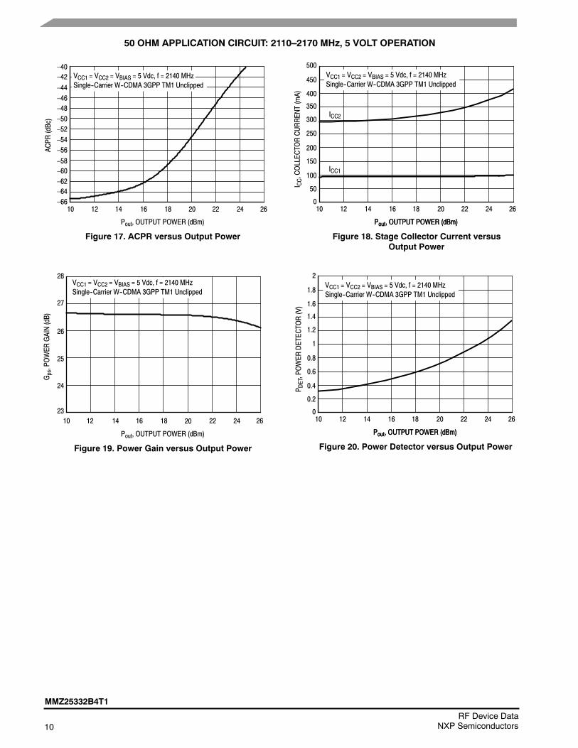
Figure 17. ACPR versus Output Power
Pout, OUTPUT POWER (dBm)
ACPR
(dBc)
2010 12 2614 16 18 22
Figure 18. Stage Collector Current versusOutput Power
Pout, OUTPUT POWER (dBm)
20
I CC,COLLECTORCURRENT(mA)
10 12 2614 16 18 22
Pout, OUTPUT POWER (dBm)
500
450
400
250
350
200
150
300
0
Figure 19. Power Gain versus Output Power
Pout, OUTPUT POWER (dBm)
27
26
25
20
Gps,POWER
GAIN(dB)
10 1223
26
24
14 16 18 22
28
VCC1 = VCC2 = VBIAS = 5 Vdc, f = 2140 MHzSingle--Carrier W--CDMA 3GPP TM1 Unclipped
VCC1 = VCC2 = VBIAS = 5 Vdc, f = 2140 MHzSingle--Carrier W--CDMA 3GPP TM1 Unclipped
ICC1
VCC1 = VCC2 = VBIAS = 5 Vdc, f = 2140 MHzSingle--Carrier W--CDMA 3GPP TM1 Unclipped
–60–62–64
ICC2
100
50
24 24
24
Figure 20. Power Detector versus Output Power
Pout, OUTPUT POWER (dBm)
20
P DET,POWER
DETECTOR(V)
10 12 2614 16 18 22
Pout, OUTPUT POWER (dBm)
2
1.8
1.6
1
1.4
0.8
0.6
1.2
0
VCC1 = VCC2 = VBIAS = 5 Vdc, f = 2140 MHzSingle--Carrier W--CDMA 3GPP TM1 Unclipped
0.4
0.2
24

MMZ25332B4T1
11RF Device DataNXP Semiconductors
50 OHM APPLICATION CIRCUIT: 2300–2400 MHz, 5 VOLT OPERATION
Figure 21. MMZ25332B4T1 Test Circuit Schematic
R1
L1
ACTIVE BIAS CIRCUIT
VCC1
Z1
L2
VBIAS
C9
PDET
C6
C1
VCC2
C3C4
C10
Z1 0.074 0.02 Microstrip
RFINPUT
RFOUTPUT
13
C5C8
C11
C214
15
16
17
18
6
5
4
3
2
1
7 8 9 10 11 12
24 23 22 21 20 19
R2
C7
Table 9. MMZ25332B4T1 Test Circuit Component Designations and ValuesPart Description Part Number Manufacturer
C1, C4 22 pF Chip Capacitors 04023J22R0BBS AVX
C2 2.0 pF Chip Capacitor 04023J2R4BBS AVX
C3 2.2 pF Chip Capacitor 04023J2R2BBS AVX
C5 8.2 pF Chip Capacitor 04023J6R8BBS AVX
C6 470 pF Chip Capacitor GRM1555C1H471JA01 Murata
C7, C8 1 F Chip Capacitors GRM155R61A105KE15 Murata
C9, C10 1000 pF Chip Capacitors GCM155R71E102KA37 Murata
C11 4.7 F Chip Capacitor GRM188R60J475KE19 Murata
L1 12 nH Chip Inductor 0603HC-12NX Coilcraft
L2 6.8 nH Chip Inductor LL1608-FSL5N6S Toko
R1 1.2 k, 1/16 W Chip Resistor RC0402JR--071K2L Yageo
R2 330 , 1/16 W Chip Resistor RC0402JR--07330L Yageo
PCB Rogers RO4350B, 0.010, r = 3.66 MG3044 MTL

12RF Device Data
NXP Semiconductors
MMZ25332B4T1
50 OHM APPLICATION CIRCUIT: 2300–2400 MHz, 5 VOLT OPERATION
C11
C8
C10C6
C5
C4
C3C2
C1
R2R1 C7
L2L1
C9
MG3044
QFN 44--24DRev. 0
RFOUTRFIN
VCC1
VDECT
VCC2
VBIAS (1)
Figure 22. MMZ25332B4T1 Test Circuit Component Layout
PCB actual size: 1.30 1.46.(1) VBIAS [Board] supplies VBA1, VBA2 and VBIAS [Device].
Table 9. MMZ25332B4T1 Test Circuit Component Designations and ValuesPart Description Part Number Manufacturer
C1, C4 22 pF Chip Capacitors 04023J22R0BBS AVX
C2 2.0 pF Chip Capacitor 04023J2R4BBS AVX
C3 2.2 pF Chip Capacitor 04023J2R2BBS AVX
C5 8.2 pF Chip Capacitor 04023J6R8BBS AVX
C6 470 pF Chip Capacitor GRM1555C1H471JA01 Murata
C7, C8 1 F Chip Capacitors GRM155R61A105KE15 Murata
C9, C10 1000 pF Chip Capacitors GCM155R71E102KA37 Murata
C11 4.7 F Chip Capacitor GRM188R60J475KE19 Murata
L1 12 nH Chip Inductor 0603HC-12NX Coilcraft
L2 6.8 nH Chip Inductor LL1608-FSL5N6S Toko
R1 1.2 k, 1/16 W Chip Resistor RC0402JR--071K2L Yageo
R2 330 , 1/16 W Chip Resistor RC0402JR--07330L Yageo
PCB Rogers RO4350B, 0.010, r = 3.66 MG3044 MTL
(Test Circuit Component Designations and Values table repeated for reference.)

MMZ25332B4T1
13RF Device DataNXP Semiconductors
50 OHM APPLICATION CIRCUIT: 2300–2400 MHz, 5 VOLT OPERATION
25002200 2300 2400
25002200 2250 2300 2350 2400 2450
Figure 23. S11 versus Frequency
2500–18
–12
2200
f, FREQUENCY (MHz)
2250
–13
–14
–15
–16
–17
S11(dB)
2300 2350
Figure 24. S21 versus Frequency
24
29
f, FREQUENCY (MHz)
28
27
26
25
S21(dB)
Figure 25. S22 versus Frequency
–32
–12
f, FREQUENCY (MHz)
–16
–20
–24
–28
S22(dB)
VCC1 = VCC2 = VBIAS = 5 Vdc VCC1 = VCC2 = VBIAS = 5 Vdc
VCC1 = VCC2 = VBIAS = 5 Vdc
2400 2450

14RF Device Data
NXP Semiconductors
MMZ25332B4T1
50 OHM APPLICATION CIRCUIT: 2300–2400 MHz, 5 VOLT OPERATION
–40
–42
–44
–56
–50
–46
–54
–52
–58
–48
–62
Figure 26. ACPR versus Output Power
Pout, OUTPUT POWER (dBm)
ACPR
(dBc)
2010 12 2414 16 18 22
Figure 27. Stage Collector Current versusOutput Power
Pout, OUTPUT POWER (dBm)
20
I CC,COLLECTORCURRENT(mA)
10 12 2414 16 18 22
Pout, OUTPUT POWER (dBm)
500
450
400
250
350
200
150
300
0
Figure 28. Power Gain versus Output Power
Pout, OUTPUT POWER (dBm)
27
26
25
20
Gps,POWER
GAIN(dB)
10 1223
24
24
14 16 18 22
28
VCC1 = VCC2 = VBIAS = 5 Vdc, f = 2350 MHzSingle--Carrier LTE--20 MHz 3GPP TM1.1, PAR = 9.8 dB
ICC1
–60
ICC2
100
50
Figure 29. Power Detector versus Output Power
Pout, OUTPUT POWER (dBm)
20
P DET,POWER
DETECTOR(V)
10 12 2414 16 18 22
Pout, OUTPUT POWER (dBm)
1.6
1
1.4
0.8
0.6
1.2
0
0.4
0.2
VCC1 = VCC2 = VBIAS = 5 Vdc, f = 2350 MHzSingle--Carrier LTE--20 MHz 3GPP TM1.1, PAR = 9.8 dB
VCC1 = VCC2 = VBIAS = 5 Vdc, f = 2350 MHzSingle--Carrier LTE--20 MHz 3GPP TM1.1, PAR = 9.8 dB
VCC1 = VCC2 = VBIAS = 5 Vdc, f = 2350 MHzSingle--Carrier LTE--20 MHz 3GPP TM1.1, PAR = 9.8 dB

MMZ25332B4T1
15RF Device DataNXP Semiconductors
Figure 30. PCB Pad Layout for 24--Lead QFN 4 4
0.50
0.30
3.00 4.40
2.6 2.6 solder pad with thermalvia structure. All dimensions in mm.
Figure 31. Product Marking
MA11WLYW
16RF Device Data
NXP Semiconductors
MMZ25332B4T1
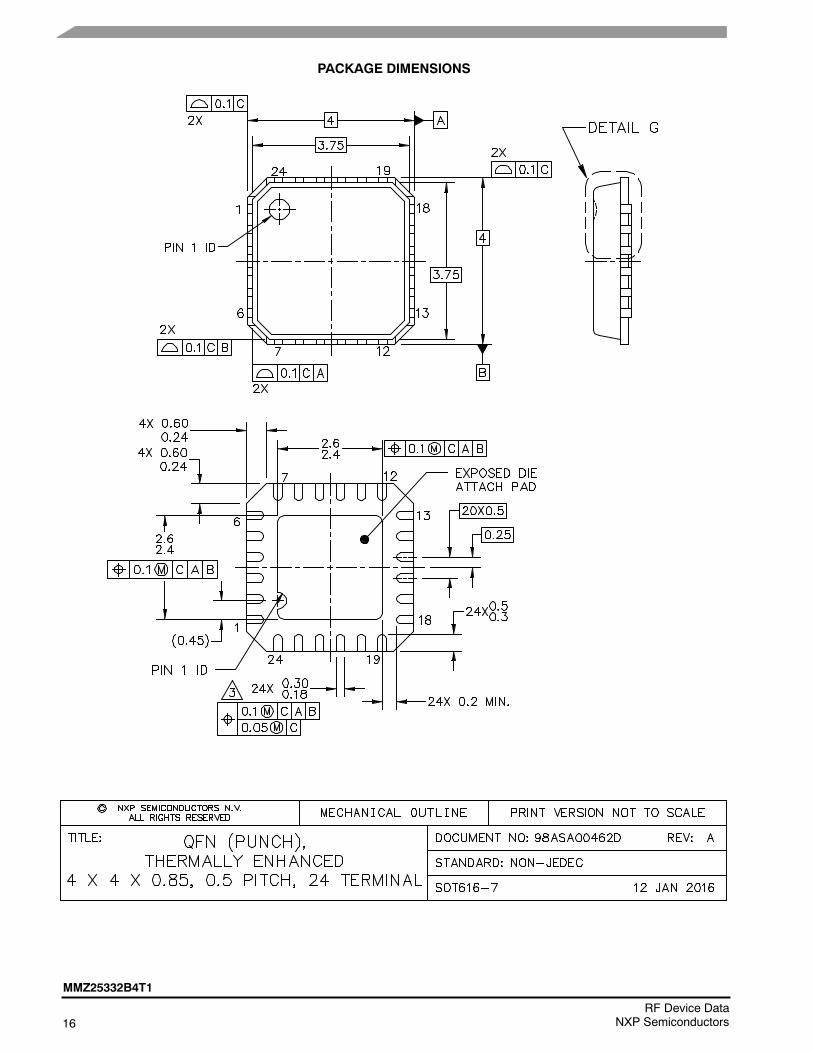
PACKAGE DIMENSIONS

MMZ25332B4T1
17RF Device DataNXP Semiconductors

18RF Device Data
NXP Semiconductors
MMZ25332B4T1

MMZ25332B4T1
19RF Device DataNXP Semiconductors
PRODUCT DOCUMENTATION, SOFTWARE AND TOOLS
Refer to the following resources to aid your design process.
Application Notes AN1955: Thermal Measurement Methodology of RF Power Amplifiers
Software .s2p File
Development Tools Printed Circuit Boards
To Download Resources Specific to a Given Part Number:1. Go to http://www.nxp.com/RF
2. Search by part number
3. Click part number link
4. Choose the desired resource from the drop down menu
FAILURE ANALYSIS
At this time, because of the physical characteristics of the part, failure analysis is limited to electrical signature analysis. Incases where NXP is contractually obligated to perform failure analysis (FA) services, full FA may be performed by thirdparty vendors with moderate success. For updates contact your local NXP Sales Office.
REVISION HISTORY
The following table summarizes revisions to this document.
Revision Date Description
0 Dec. 2015 Initial Release of Data Sheet
1 Dec. 2017 Fig. 31, Product Marking: updated to show location of Pin 1 on Product Marking, p. 15

20RF Device Data
NXP Semiconductors
MMZ25332B4T1
Information in this document is provided solely to enable system and softwareimplementers to use NXP products. There are no express or implied copyright licensesgranted hereunder to design or fabricate any integrated circuits based on the informationin this document. NXP reserves the right to make changes without further notice to anyproducts herein.
NXP makes no warranty, representation, or guarantee regarding the suitability of itsproducts for any particular purpose, nor does NXP assume any liability arising out of theapplication or use of any product or circuit, and specifically disclaims any and all liability,including without limitation consequential or incidental damages. “Typical” parametersthat may be provided in NXP data sheets and/or specifications can and do vary indifferent applications, and actual performance may vary over time. All operatingparameters, including “typicals,” must be validated for each customer application bycustomer’s technical experts. NXP does not convey any license under its patent rightsnor the rights of others. NXP sells products pursuant to standard terms and conditions ofsale, which can be found at the following address: nxp.com/SalesTermsandConditions.
NXP, the NXP logo, Freescale and the Freescale logo are trademarks of NXP B.V.All other product or service names are the property of their respective owners.E 2015, 2017 NXP B.V.
How to Reach Us:
Home Page:nxp.com
Web Support:nxp.com/support
Document Number: MMZ25332B4Rev. 1, 12/2017