Embed Size (px)
Citation preview

2. Transistors, Fabrication, Layout
Jacob Abraham
Department of Electrical and Computer EngineeringThe University of Texas at Austin
VLSI DesignFall 2017
September 6, 2017
ECE Department, University of Texas at Austin Lecture 2. Transistors, Fabrication, Layout Jacob Abraham, September 6, 2017 1 / 44

Conductivity in Silicon Lattice
Look at the behavior of crystalline silicon
At temperatures close to 0 K, electrons in outermost shelltightly bound (insulator)
At higher temps., (300 K), some electrons have thermalenergy to break covalent bonds
ECE Department, University of Texas at Austin Lecture 2. Transistors, Fabrication, Layout Jacob Abraham, September 6, 2017 1 / 44

The Elements (Periodic Table)
ECE Department, University of Texas at Austin Lecture 2. Transistors, Fabrication, Layout Jacob Abraham, September 6, 2017 2 / 44

Build Systems with Information on ElectricalCharacteristics of Building Blocks (Transistors)
This course will not cover semiconductor physics
Learn this from other courses in the department
We will design VLSI circuits knowing the electrical behavior ofthe transistors
ECE Department, University of Texas at Austin Lecture 2. Transistors, Fabrication, Layout Jacob Abraham, September 6, 2017 3 / 44

Dopants
Used to selectively change the conductivity of silicon
Silicon is a semiconductor
Pure silicon has no free carriers and conducts poorly
Adding dopants impurities to pure silicon increases theconductivity
Group V: extra electron (n-type)
Group III: missing electron, called hole (p-type)
ECE Department, University of Texas at Austin Lecture 2. Transistors, Fabrication, Layout Jacob Abraham, September 6, 2017 4 / 44

p-n Junctions
Diodes
A junction between p-type and n-type semiconductor forms adiode
Current flows only in one direction
ECE Department, University of Texas at Austin Lecture 2. Transistors, Fabrication, Layout Jacob Abraham, September 6, 2017 5 / 44

p-n Junction, Cont’d
Source: Prof. Dr. Helmut Foll, University of KielECE Department, University of Texas at Austin Lecture 2. Transistors, Fabrication, Layout Jacob Abraham, September 6, 2017 6 / 44

nMOS Transistor
Four-Terminal device: gate, source, drain, body
Gate oxide body stack looks like a capacitor
Gate and body are conductors
SiO2 (oxide) is a very good insulator
Called metal oxide semiconductor (MOS) capacitor, eventhough gate material changed to polysilicon
Recent gate material in nanoscale processes is back to metal
ECE Department, University of Texas at Austin Lecture 2. Transistors, Fabrication, Layout Jacob Abraham, September 6, 2017 7 / 44

nMOS Transistor Operation
Body (bulk) is commonly tied to Ground (0 V)
When the gate is at a low voltage
P-type body is at low voltage
Source-body and drain-body diodes are OFF
No current flows, transistor is OFF
When the gate is at a high voltage
Positive charge on gate of MOScapacitor
Negative charge attracted to body
Inverts a channel under gate to n-type
Now electrons can flow through n-typesilicon from source through channel todrain, transistor is ON
ECE Department, University of Texas at Austin Lecture 2. Transistors, Fabrication, Layout Jacob Abraham, September 6, 2017 8 / 44

pMOS Transistor
Similar to nMOS transistor, but doping and voltages reversed
Body tied to high voltage (VDD)
Gate low: transistor ON
Gate high: transistor OFF
Bubble indicates inverted behavior
ECE Department, University of Texas at Austin Lecture 2. Transistors, Fabrication, Layout Jacob Abraham, September 6, 2017 9 / 44

CMOS Fabrication
Silicon technology
CMOS transistors are fabricated on silicon wafer
Lithography process similar to printing press
On each step, different materials are deposited or etched
Easiest to understand by viewing both top and cross-sectionof wafer in a simplified manufacturing process
Example inverter cross-section
Typically use p-type substrate for nMOS transistors
Requires n-well for body of pMOS transistors
n+
p substrate
p+
n well
A
YGND VDD
n+ p+
SiO2
n+ diffusion
p+ diffusion
polysilicon
metal1
nMOS transistor pMOS transistor
ECE Department, University of Texas at Austin Lecture 2. Transistors, Fabrication, Layout Jacob Abraham, September 6, 2017 10 / 44

Well and Substrate Taps
Substrate contacts are critical to correct operation of CMOS
Substrate must be tied to GND, n-well to VDD(reverse-biased diodes isolate regions)
Metal to lightly-doped semiconductor forms poor connectioncalled Schottky Diode – use heavily doped well and substratecontacts/taps
n+
p substrate
p+
n well
A
YGND VDD
n+p+
substrate tap well tap
n+ p+
ECE Department, University of Texas at Austin Lecture 2. Transistors, Fabrication, Layout Jacob Abraham, September 6, 2017 11 / 44

Inverter Masks
Transistors and wires are defined by masks
Cross-sections shown above taken along dashed line
ECE Department, University of Texas at Austin Lecture 2. Transistors, Fabrication, Layout Jacob Abraham, September 6, 2017 12 / 44

Examples of Fabrication Steps
Start with blank wafer
Build inverter from the bottom up
First step is to form the n-well
Cover wafer with protective layer of SiO2 (oxide)
Remove layer where n-well should be built
Implant or diffuse n dopants into exposed wafer
Strip off SiO2
ECE Department, University of Texas at Austin Lecture 2. Transistors, Fabrication, Layout Jacob Abraham, September 6, 2017 13 / 44

Oxidation and Photoresist
Grow SiO2 on top of Si wafer
900 −− 1200◦C with H2O or O2 in oxidation furnace
Spin-on photoresist
Photoresist is a light-sensitive organic polymer which softenswhere exposed to light (positive resist)
ECE Department, University of Texas at Austin Lecture 2. Transistors, Fabrication, Layout Jacob Abraham, September 6, 2017 14 / 44

Lithography
Use light to transfer a pattern to the wafer
Expose photoresist through n-well mask (using UV light –example 193 nm wavelength)
“Immersion lithography” used in some nanoscale processes
Strip off exposed photoresist
Interesting physics problem
How can we “print” a 45 nm feature using light with awavelength of 193 nm?
Significant distortion of the image!ECE Department, University of Texas at Austin Lecture 2. Transistors, Fabrication, Layout Jacob Abraham, September 6, 2017 15 / 44

Trend in Integrated Circuit Feature Sizes
ECE Department, University of Texas at Austin Lecture 2. Transistors, Fabrication, Layout Jacob Abraham, September 6, 2017 16 / 44

Features Smaller than Wavelength of Light Used
ECE Department, University of Texas at Austin Lecture 2. Transistors, Fabrication, Layout Jacob Abraham, September 6, 2017 17 / 44

Optical Proximity Correction (OPC)
What you see is NOT what you get
ECE Department, University of Texas at Austin Lecture 2. Transistors, Fabrication, Layout Jacob Abraham, September 6, 2017 18 / 44

Etch and Strip Photoresist
Etch oxide with Hydrofluoric acid (HF)
Only attacks oxide where resist has been exposed
Strip remaining photoresist using mixture of acids (“piranha” etch)
Necessary so resist does not melt in the next step
ECE Department, University of Texas at Austin Lecture 2. Transistors, Fabrication, Layout Jacob Abraham, September 6, 2017 19 / 44

n-Well
Formed using ion implant (used to be diffusion)
Bombard wafer with As ions, which only enter exposed Si
(With diffusion, wafer is placed in a furnace with As gas)
Remaining oxide is then stripped off using HF, and it is backto the bare wafer, but with an n-well
Subsequent steps repeat the above process
ECE Department, University of Texas at Austin Lecture 2. Transistors, Fabrication, Layout Jacob Abraham, September 6, 2017 20 / 44
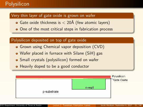
Polysilicon
Very thin layer of gate oxide is grown on wafer
Gate oxide thickness is < 20A (few atomic layers)
One of the most critical steps in fabrication process
Polysilicon deposited on top of gate oxide
Grown using Chemical vapor deposition (CVD)
Wafer placed in furnace with Silane (SiH) gas
Small crystals (polysilicon) formed on wafer
Heavily doped to be a good conductor
ECE Department, University of Texas at Austin Lecture 2. Transistors, Fabrication, Layout Jacob Abraham, September 6, 2017 21 / 44

Polysilicon Patterning
Use same lithography processing to pattern polysilicon
Reactive Ion Etch (RIE) process
Charge buildup on un-etched polysilicon can lead to “antennaeffects” and damage gate oxide
Self-aligned process
Polysilicon “blocks” dopants where the channel should beformed
ECE Department, University of Texas at Austin Lecture 2. Transistors, Fabrication, Layout Jacob Abraham, September 6, 2017 22 / 44

N+ Diffusion
nMOS transistors are formed
Oxide is patterned to form the n+ regions
N+ diffusion forms nMOS source, drain, and n-well contact
ECE Department, University of Texas at Austin Lecture 2. Transistors, Fabrication, Layout Jacob Abraham, September 6, 2017 23 / 44

N+ Diffusion, Cont’d
Ion implantation used to dope silicon
n+ regions are formed
Oxide is stripped off to complete patterning step
ECE Department, University of Texas at Austin Lecture 2. Transistors, Fabrication, Layout Jacob Abraham, September 6, 2017 24 / 44

P+ Diffusion
A similar set of steps is used to form the p+ diffusion regions forthe pMOS transistor source and drain as well as the substratecontact
ECE Department, University of Texas at Austin Lecture 2. Transistors, Fabrication, Layout Jacob Abraham, September 6, 2017 25 / 44

Contacts
Points where the first level of metal contacts the transistors
Used to wire the devices together
Wafer is covered with thick field oxide
Oxide is etched where the contact cuts are needed
ECE Department, University of Texas at Austin Lecture 2. Transistors, Fabrication, Layout Jacob Abraham, September 6, 2017 26 / 44

Metalization
Used to interconnect internal nodes
Aluminum was the traditional metal
Switch to Copper for high performance processes
Aluminum is sputtered over the entire wafer
Patterned to remove excess metal, leaving the wires
ECE Department, University of Texas at Austin Lecture 2. Transistors, Fabrication, Layout Jacob Abraham, September 6, 2017 27 / 44

Layout
Describes actual layers and geometry on the silicon substrateto implement a function
Need to define transistors, interconnection
Transistor widths (for performance)Spacing, interconnect widths, to reduce defects, satisfy powerrequirementsContacts (between poly or active and metal), and vias(between metal layers)Wells and their contacts (to power or ground)
Layout of lower-level cells constrained by higher-levelrequirements: floorplanning
“design iteration”
ECE Department, University of Texas at Austin Lecture 2. Transistors, Fabrication, Layout Jacob Abraham, September 6, 2017 28 / 44
Layout, Cont’d
Chips are specified with set of masks
Minimum dimensions of masks determine transistor size (andhence speed, cost, and power)
Feature size f = distance between source and drain
Set by minimum width of polysilicon (= minimum “drawn”gate length)
Feature size improves 30% every 3 years or so
Normalize for feature size when describing design rules
Express rules in terms of λ = f/2
e.g., λ = 0.3µm in 0.6µm process
ECE Department, University of Texas at Austin Lecture 2. Transistors, Fabrication, Layout Jacob Abraham, September 6, 2017 29 / 44

CMOS Inverter Layout
Note: the N- and P- well arenot shown in the layout
ECE Department, University of Texas at Austin Lecture 2. Transistors, Fabrication, Layout Jacob Abraham, September 6, 2017 30 / 44

Other CMOS Layouts
Using wide transistors Using even wider transistors
ECE Department, University of Texas at Austin Lecture 2. Transistors, Fabrication, Layout Jacob Abraham, September 6, 2017 31 / 44

Buffer with Two Inverters
Side by side Stacked
ECE Department, University of Texas at Austin Lecture 2. Transistors, Fabrication, Layout Jacob Abraham, September 6, 2017 32 / 44

Improving Layout Efficiency
“Flip” a cell so that power (or ground) can be shared with anothercell
ECE Department, University of Texas at Austin Lecture 2. Transistors, Fabrication, Layout Jacob Abraham, September 6, 2017 33 / 44

“Stick” Diagram and Simplified Layout of NAND Gate
Stick diagrams identifyactual layers (which aschematic does not);both can be annotatedwith transistor sizes
n- and p-wells are shown
ECE Department, University of Texas at Austin Lecture 2. Transistors, Fabrication, Layout Jacob Abraham, September 6, 2017 34 / 44

Simplified Design Rules
Based on λ (popular in academia)
Discussed in the textbook
Rules based on λ can theoretically be migrated to a differenttechnology (by changing the value of λ); in practice, all the rulesdo not scale in the same way, and industry typically does not use λrules
ECE Department, University of Texas at Austin Lecture 2. Transistors, Fabrication, Layout Jacob Abraham, September 6, 2017 35 / 44

Inverter Layout
Dimensions of pMOS and nMOS transistors
Dimensions specified as Width/Length (WL )
Minimum size, 4λ/2λ, sometimes called unit-size transistor(pMOS transistors are typically designed to be about twice thewidth of nMOS transistors, because of the mobilities of holesand electrons)
ECE Department, University of Texas at Austin Lecture 2. Transistors, Fabrication, Layout Jacob Abraham, September 6, 2017 36 / 44

The MOSIS Scalable CMOS Rules
MOSIS is a prototyping and small-volume production service forVLSI circuit development
MOSIS keeps costs down by combining many designs on asingle die (multi-project chips)
Similar facilities exist in Europe (Europractice, CMP), Taiwan,etc.
λ-based rules
Designs using these rules are fabricated by a variety ofcompanies
Support for submicron digital CMOS, analog (buried polylayer for capacitor), micromachines, etc.
https://www.mosis.com/files/scmos/scmos.pdf
ECE Department, University of Texas at Austin Lecture 2. Transistors, Fabrication, Layout Jacob Abraham, September 6, 2017 37 / 44

Nangate 45nm Open Cell Library
Used in the laboratory exercises
This is an open-source, standard-cell library
To aid university research programs and other organizations indeveloping design flows, designing circuits and exercising newalgorithms
Link to the wiki:http://www.eda.ncsu.edu/wiki/FreePDK45:Contents
Example: poly rules (note: summarized here)
Rule Value Description1 50 nm Minimum width2 140 nm Minimum spacing3 55 nm Min. extension4 70 nm Min. enclosure5 50 nm Min. spacing6 75 nm Min. spacing
ECE Department, University of Texas at Austin Lecture 2. Transistors, Fabrication, Layout Jacob Abraham, September 6, 2017 38 / 44

Example of Other Nangate 45nm Rules
Active RulesRule Value Description1 90 nm Minimum width2 80 nm Minimum spacing3 – Min. well-active4 – active inside
Contact RulesRule Value Description1 65 nm Minimum width2 75 nm Minimum spacing3 – contact inside4 5 nm Min. active around5 5 nm Min. poly around6 35 nm Min. spacing with gate7 90 nm Min. spacing with poly
ECE Department, University of Texas at Austin Lecture 2. Transistors, Fabrication, Layout Jacob Abraham, September 6, 2017 39 / 44

Trend Towards Reducing Number of Rules
Improve manufacturability
Less flexibility for designers
Intel reduced the number of poly layout rules for logic layoutin 45nm by 37% compared with the 65 nm process
Highly regular layout greatly reduces lithographic distortions
Limit rules, thereby limiting the number of allowed structuresand shape relationshipsMove towards 1-dimensional shapes and “Gridded DesignRules” (GDR)
Example layout from Tela Innovations
ECE Department, University of Texas at Austin Lecture 2. Transistors, Fabrication, Layout Jacob Abraham, September 6, 2017 40 / 44

Regular Layout
Lithography simulations
Lithographic distortions reduced significantly with 1-D shapesand GDR
Scan D Flip-Flop, 45nm process
Source: Tela Innovations, Inc., ISPD 2009
2D Conven-tionalLayout
1D GDRLayout
ECE Department, University of Texas at Austin Lecture 2. Transistors, Fabrication, Layout Jacob Abraham, September 6, 2017 41 / 44

Copper and the Damascene ProcessSource: UMC
Layers of Damascene Copper (Intel)
Copper Damascene Interconnect (Intel)
ECE Department, University of Texas at Austin Lecture 2. Transistors, Fabrication, Layout Jacob Abraham, September 6, 2017 42 / 44

Advanced Metalization
IBM Technology (in Rabaey, Digital Integrated Circuits, 2nd ed.)First commercial Copper process(0.12µ)
ECE Department, University of Texas at Austin Lecture 2. Transistors, Fabrication, Layout Jacob Abraham, September 6, 2017 43 / 44

Example CMOS Circuit
ECE Department, University of Texas at Austin Lecture 2. Transistors, Fabrication, Layout Jacob Abraham, September 6, 2017 44 / 44