Embed Size (px)
Citation preview

Calhoun: The NPS Institutional Archive
Theses and Dissertations Thesis Collection
2001-03
2-D modeling of GaN HEMTs incorporating the
piezoelectric effect
Eimers, Karl P.
Monterey, California. Naval Postgraduate School
http://hdl.handle.net/10945/2751

NAVAL POSTGRADUATE SCHOOL Monterey, California
THESIS
Approved for public release; distribution is unlimited.
2-D MODELING OF GaN HEMTS INCORPORATING THE PIEZOELECTRIC EFFECT
by
Karl P. Eimers
March 2001
Thesis Advisor: Todd R. Weatherford Second Reader: Harry Dietrich

2-D MODELING OF GaN HEMTS INCORPORATING THE PIEZOELECTRIC EFFECT
Karl P. Eimers-Lieutenant, United States Navy B.S., United States Military Academy, 1992
Master of Science in Electrical Engineering-March 2001 Advisor: Todd R. Weatherford, Department of Electrical and Computer Engineering
Second Reader: Harry Dietrich, Naval Research Laboratory Gallium Nitride (GaN) High Electron Mobility Transistors (HEMTs) are microwave power devices that promise to revolutionize the capability of Navy radar systems. The Office of Naval Research is currently funding basic research of developing microwave power amplifiers for use in future radar systems. This thesis incorporates piezoelectric (PZ) equations in the Silvaco AtlasTM software for modeling GaN/AlGaN structures. The PZ effect enhances a two dimensional electron gas at the GaN/AlGaN interface due to stress induced polarization.
DoD KEY TECHNOLOGY AREAS: Electronics, Materials, Processes, and Structures, Modeling and Simulation KEYWORDS: Gallium Nitride, High Electron Mobility Transistor, Piezoelectric Effect
i
REPORT DOCUMENTATION PAGE Form Approved OMB No. 0704-0188 Public reporting burden for this collection of information is estimated to average 1 hour per response, including the time for reviewing instruction, searching existing data sources, gathering and maintaining the data needed, and completing and reviewing the collection of information. Send comments regarding this burden estimate or any other aspect of this collection of information, including suggestions for reducing this burden, to Washington headquarters Services, Directorate for Information Operations and Reports, 1215 Jefferson Davis Highway, Suite 1204, Arlington, VA 22202-4302, and to the Office of Management and Budget, Paperwork Reduction Project (0704-0188) Washington DC 20503. 1. AGENCY USE ONLY (Leave blank)
2. REPORT DATE March 2001
3. REPORT TYPE AND DATES COVERED Master�s Thesis
4. TITLE AND SUBTITLE: Title (Mix case letters) 2-D Modeling of GaN HEMTs Incorporating the Piezoelectric Effect 6. AUTHOR(S) Eimers, Karl P.
5. FUNDING NUMBERS
7. PERFORMING ORGANIZATION NAME(S) AND ADDRESS(ES) Naval Postgraduate School Monterey, CA 93943-5000
8. PERFORMING ORGANIZATION REPORT NUMBER
9. SPONSORING / MONITORING AGENCY NAME(S) AND ADDRESS(ES) N/A
10. SPONSORING / MONITORING AGENCY REPORT NUMBER
11. SUPPLEMENTARY NOTES The views expressed in this thesis are those of the author and do not reflect the official policy or position of the Department of Defense or the U.S. Government. 12a. DISTRIBUTION / AVAILABILITY STATEMENT Approved for public release; distribution is unlimited
12b. DISTRIBUTION CODE A
13. ABSTRACT (maximum 200 words) Gallium Nitride (GaN) High Electron Mobility Transistors (HEMTs) are microwave power devices that promise to revolutionize the capability of Navy radar systems. The Office of Naval Research is currently funding basic research of developing microwave power amplifiers for use in future radar systems. This thesis incorporates piezoelectric (PZ) equations in the Silvaco AtlasTM software for modeling GaN/AlGaN structures. The PZ effect enhances a two dimensional electron gas at the GaN/AlGaN interface due to stress induced polarization.
15. NUMBER OF PAGES
14. SUBJECT TERMS Gallium Nitride, High Electron Mobility Transistor, Piezoelectric effect
16. PRICE CODE
17. SECURITY CLASSIFICATION OF REPORT
Unclassified
18. SECURITY CLASSIFICATION OF THIS PAGE
Unclassified
19. SECURITY CLASSIFICATION OF ABSTRACT
Unclassified
20. LIMITATION OF ABSTRACT
UL
NSN 7540-01-280-5500 Standard Form 298 (Rev. 2-89) Prescribed by ANSI Std. 239-18

ii
THIS PAGE INTENTIONALLY LEFT BLANK

iii
Approved for public release; distribution is unlimited
2-D MODELING OF GaN HEMTS INCORPORATING THE PIEZOELECTRIC EFFECT
Karl P. Eimers
Lieutenant, United States Navy B.S., United States Military Academy, 1992
Submitted in partial fulfillment of the requirements for the degree of
MASTER OF SCIENCE IN ELECTRICAL ENGINEERING
from the
NAVAL POSTGRADUATE SCHOOL March 2001
Author: ___________________________________________ Karl P. Eimers
Approved by: ___________________________________________ Todd Weatherford, Thesis Advisor
___________________________________________ Harry Dietrich, Second Reader
___________________________________________ Jeffrey B. Knorr, Chairman
Department of Electrical and Computer Engineering

iv
THIS PAGE INTENTIONALLY LEFT BLANK

v
ABSTRACT Gallium Nitride (GaN) High Electron Mobility Transistors (HEMTs) are
microwave power devices that promise to revolutionize the capability of Navy radar
systems. The Office of Naval Research is currently funding basic research of developing
microwave power amplifiers for use in future radar systems. This thesis incorporates
piezoelectric (PZ) equations in the Silvaco ATLASTM software for modeling GaN/AlGaN
structures. The PZ effect enhances a two dimensional electron gas at the GaN/AlGaN
interface due to stress induced polarization.

vi
THIS PAGE INTENTIONALLY LEFT BLANK

vii
TABLE OF CONTENTS
I. INTRODUCTION....................................................................................................... 1 A. BACKGROUND.............................................................................................. 1 B. RELATED WORK ......................................................................................... 3 C. OBJECTIVES ................................................................................................. 3
II. TRANSISTOR OVERVIEW ..................................................................................... 5 A. FIELD EFFECT TRANSISTOR................................................................... 5 B. HIGH ELECTRON MOBILITY TRANSISTOR........................................ 8 C. GALLIUM NITRIDE ................................................................................... 10 D. PIEZOELECTRIC EFFECT....................................................................... 12
III. DEVICE MODELING.............................................................................................. 15 A. GENERAL ..................................................................................................... 15 B. NUMERICAL SIMULATION MODELS .................................................. 16
1. Boltzmann Approximation of Electron Probability....................... 16 2. Various ............................................................................................... 16 3. Solution Convergence ....................................................................... 17
C. PIEZOELECTRIC EFFECT....................................................................... 17 1. General ............................................................................................... 17 2. Sheet Carrier Concentration due to Internal Stress ...................... 18
III. RESULTS................................................................................................................... 25 A. THE MODEL ................................................................................................ 25 B. 2-DEG............................................................................................................. 27 C. IV CURVES................................................................................................... 34
IV. DISCUSSION ............................................................................................................ 37 VI. CONCLUSIONS AND RECOMMENDATIONS.................................................. 41
A. CONCLUSIONS ........................................................................................... 41 B. RECOMMENDATIONS.............................................................................. 41
LIST OF REFERENCES ..................................................................................................... 43 APPENDIX A. DECKBUILD SIMULATION INPUT DECK......................................... 45 APPENDIX B. C-INTERPRETER FILE ........................................................................... 47 INITIAL DISTRIBUTION LIST ........................................................................................ 55

viii
THIS PAGE INTENTIONALLY LEFT BLANK

ix
LIST OF FIGURES
Figure 1. Basic FET structure. ................................................................................................ 5 Figure 2. Energy band diagram for FET with no bias at gate contact...................................... 7 Figure 3. A HEMT or MODFET structure (From: Silvaco Software example files). ........... 8 Figure 4. Energy band diagram for unbiased HEMT device. .................................................. 9 Figure 5. Energy band diagram for a HEMT with 2 volt bias at drain. ................................. 10 Figure 6. PZ effect demonstrated as increase in polarization due to mechanical stress. ....... 13 Figure 7. EF(x) calculated from Ambacher and EF(x) modeled for this work versus Al
mole fraction. .................................................................................................. 22 Figure 8. A typical NRL AlGaN/GaN HEMT. ...................................................................... 25 Figure 9. HEMT model created in Silvaco software.............................................................. 26 Figure 10. Close view of HEMT contacts from same model................................................. 26 Figure 11. Bandgaps of various models. ................................................................................ 27 Figure 12. Donor concentration profile of various models. ................................................... 29 Figure 13. Donor concentration spike at interface of various models. .................................. 30 Figure 14. Electron concentrations versus distance of various models.................................. 31 Figure 15. Electron concentrations at the interface of various models. ................................. 32 Figure 16. Conduction and valence band energy versus distance of various models. ........... 33 Figure 17. Conduction band energy of various models (close up)......................................... 34 Figure 18. Simulated IV curves for AlGaN HEMT transistor. .............................................. 35 Figure 19. Measured IV curves for AlGaN HEMT transistor................................................ 35 Figure 20. Simulated and measured IV curves for AlGaN HEMT transistor. ....................... 36

x
THIS PAGE INTENTIONALLY LEFT BLANK

xi
LIST OF TABLES
Table 1. 2-DEG versus Fermi level........................................................................................ 21 Table 2. Variables, sources, and parameters. .......................................................................... 23

xii
THIS PAGE INTENTIONALLY LEFT BLANK
xiii
ACKNOWLEDGMENTS I sincerely thank the following people who assisted me to complete this thesis:
Prof. Weatherford provided clear guidance, kept the project on track, and ensured the
quality of the final product. Dr. Harry Dietrich kindly assisted with the content and
coordination with the Naval Research Laboratory. Dr. Steve Binari provided the vital
data for comparison between simulated results and real device measurements. Dr. Mario
Ancona graciously provided a prototype GaN HEMT model and advice in using Silvaco
Software. Dr.�s Weber, Specht, Feick, et al, of the University of California, Berkeley
provided needed insight in material properties of GaN and the piezoelectric effect.
Maureen Stafford Eimers made life a blessing, while Zachary Eimers provided all the
necessary diversions to keep things in perspective. Most of all, I thank God who made
everything and gives me reason to be.

xiv
EXECUTIVE SUMMARY
A computer model of Gallium Nitride (GaN) High Electron Mobility Transistors (HEMTs) has been developed for the purpose of designing and modifying high power and high frequency power amplifiers. GaN HEMT power amplifiers are being investigated for the Advanced Multi-function RF System (AMRFS). This model includes the impact of the piezoelectric effect automatically based on the material parameters of the GaN HEMT.
The piezoelectric effect results from the GaN noncentrosymmetric crystal
combined with strain induced at the AlGaN/GaN heterojunction by lattice mismatch. This effect results in a predictable amount of electron sheet charge at the heterojunction providing exceptional conductivity of electron current. GaN material offers large energy bandgap, high breakdown voltage, and high peak electron velocity. The heterojunction also produces a quantum well which further enhances the speed of electron transport from source to drain contacts.
Silvaco software was modified to incorporate these physical realities. Equations
generated by Prof. Ambacher of Cornell University utilize the mole fraction of Aluminum in the AlGaN layer and the thickness of that layer to accurately predict the resultant amount of two dimensional electron gas (2-DEG). The software modifications use that result and simulate implanting an appropriate amount of donor impurities in the top 10 nanometers of GaN material that lies directly below the AlGaN layer. The software incorporates these calculations when first generating the device for simulation. Once the software begins executing voltage biasing commands, electron mobility and electron saturation velocity values are manually controlled to avoid the expected scattering effects that impurity implantation would normally instigate.
Simulations were run on a model based on actual devices produced and tested at
the Naval Research Laboratory (NRL). Various levels of Aluminum mole fraction were tried and resulted in electron concentrations expected by the Ambacher equations. Electron concentrations were found to match the program generated donor implantation within 4% accuracy. Energy band diagrams were generated to verify proper electron energy levels expected for a HEMT device. The program proved capable of matching expected energy band profiles throughout various mole fraction levels.
A model based on NRL�s devices with a matching mole fraction was run through
drain-to-source bias conditions and compared with measured results provided by NRL. The device was simulated under matching gate biases and I-V curves presented to show a general correspondence between modeled and measured results. Numerous combinations of electron mobility and velocity saturation were tried to improve model accuracy. Results presented derive from a simulation run with reported values of mobility and velocity saturation. Possibilities for improving model accuracy are discussed and evaluated for further research.

xv
This work is the only reported software model that incorporates the piezoelectric effect. GaN HEMT performance is strongly related to the piezoelectric effect which governs the amount of charge carriers available in the device. Since the GaN HEMT promises to be the most powerful available high frequency power amplifier, it is hoped this work will be an important step forward in realizing the potential of this new device.

xvi
THIS PAGE INTENTIONALLY LEFT BLANK

1
I. INTRODUCTION
A. BACKGROUND
Radio Frequency (RF) amplifiers are vital to Navy technology requirements. The
Navy employs many systems that radiate RF energy for communication, navigation, or
detection and ranging. RF waveforms used by these systems are typically formed by
delicate mechanisms at minimal power; so, virtually every RF emission is amplified
before transmission. Often this amplification has been done by travelling-wave tube
(TWT) technology, which is expensive and readily degrades over time.
Solid state amplifiers offer a promising alternative to TWTs. Incorporating
smaller size and higher reliability, semiconductor amplifiers offer easier manufacturing,
packaging, and handling than tubes. These amplifiers cannot currently match the
maximum amplification of TWTs, yet they demonstrate respectable power levels with
less distortion than TWTs, especially over extended periods of time [1].
Field Effect Transistors (FETs) are excellent RF power amplifiers especially
above 4 GHz and where low noise is particularly vital. Generally, FETs have superior
power gains, lower noise, and higher output power capabilities than their chief
competitor, the bipolar junction transistor (BJT) [2]. The FET benefits in speed and noise
from its single carrier (unipolar) process.
High Electron Mobility Transistors (HEMTs) are the most promising high-speed
power amplifiers yet seen. The HEMT, while a relatively immature technology, has the
highest current-gain cutoff frequency yet measured for any semiconductor device. The
HEMT uses an energy offset that occurs between the substrate material and its upper

2
layer of Aluminum alloy (which is doped in a special way; this modulated doping gives
rise the HEMT�s other name, the MODFET). Since the GaN substrate material is nearly
or completely undoped, the highest possible electron mobility and least amount of
scattering are achieved.
Non-Silicon semiconductors dominate the high power, high frequency amplifier
environment. Compound semiconductors such as Gallium Arsenide are more difficult to
manufacture but offer advantages in material parameters such as electron mobility
allowing greater gain and faster operation. Gallium Nitride (GaN) is a different
compound semiconductor that has promise to be the ultimate in RF amplification because
of its high frequency and high temperature capability and extremely high power output.
Software modeling is a versatile tool for designing and analyzing semiconductor
devices. Parameters that can be calculated include DC characteristics such as threshold
voltage, gain, leakage, punch through voltage and breakdown behavior. RF
characteristics that can be predicted include cut-off frequency, s-, y-, h- and z-parameters,
maximum available gain, maximum stable gain, maximum frequency of oscillation and
stability factor. Intrinsic switching times and Fourier analysis of periodic large-signal
outputs can also be calculated.
High power GaN microwave devices require special attention for accurate
modeling. Heat is a crucial parameter in predicting device performance for high-power,
high-speed devices. The piezoelectric (PZ) effect has never been modeled in a
Technology Computer Aided Design (TCAD) program yet may be the key to designing
GaN-based compound semiconductor devices. The PZ effect refers to the physical
property of some materials, GaN in particular, to exhibit polarization when strained. This

3
polarization results in lowered resistivity due to the presence of extra charge carriers.
Since GaN and AlGaN have a slight lattice mismatch, every HEMT structure exhibits the
PZ effect. Adding mechanical strain to a device might further enhance PZ effect.
B. RELATED WORK
The Naval Research Laboratory is currently conducting research on GaN HEMT
power amplifiers. They are using Silvaco Software to model devices that they have built
or intend to build. NRL�s models do not automatically account for the piezoelectric
effect. This work hopes to dovetail their efforts and take a further step in accurately
replicating the GaN HEMT.
UC Berkeley is conducting tests of compound semiconductor materials to include
Gallium Nitride. They are conducting tests that apply mechanical stress to materials and
measuring various constants related to the piezoelectric effect. Their testing of GaN and
AlGaN materials under applied stress could assist in accurately modeling externally
applied stress effects. This work currently focuses on internal stresses generated by
lattice mismatch between AlGaN and GaN heterojunctions.
C. OBJECTIVES
This work seeks to increase the Navy�s capability to model GaN HEMTs by
providing a working Silvaco Software model of an existing GaN HEMT device. The
model developed is distinguished in that it incorporates the piezoelectric effect.

4
THIS PAGE INTENTIONALLY LEFT BLANK

5
II. TRANSISTOR OVERVIEW
The following sections describe the basic structure and operation of field effect
transistors and the high electron mobility transistor.
A. FIELD EFFECT TRANSISTOR
The FET was the original transistor, or transfer resistor, despite the earlier
maturing of the bipolar junction transistor. The FET was first conceived in the 1920�s,
but it was not seriously developed until the 1960�s. In between those time periods, the
BJT emerged and blossomed into an effective electronic component. Regardless of
temporarily losing prominence to the BJT as the electronic device of choice, the FET has
regained distinction by its compactness and by easier production. Thanks to the
computer industry, the FET (specifically the MOSFET) is currently the most produced
manmade object in the world [3].
Figure 1. Basic FET structure.
The FET operates by separating metal contacts (source and drain) by a piece of
semiconductor. Another contact (non-conducting gate) modulates the
conductance/resistance of the semiconductor material by applying a voltage and thereby
modulating the current flow between the original two contacts. As shown in Figure 1,
MetalContact
A.
Semi-conductor
B.
ModulatingContact
MetalContactCurrent
SourceDrain
Gate

6
electric current entering the FET can either be allowed to flow through, be restricted, or
be shut off depending on the voltage applied at the modulating contact.
This device works because the modulating contact voltage controls the amount of
depletion region present in the semiconductor. In order to induce current flowing in the
semiconductor, a voltage difference must exist between the source and drain. The gate to
drain voltage difference will cause a depletion region (or an inversion layer) to build
around the modulating gate contact (which is grounded). If the modulating contact is
biased opposite the voltage difference between the other contacts, the depletion region
grows. As soon as a depletion region completely covers, or pinches off the channel of
current carriers, the amount of current flowing from source to drain is limited to its
existing level. If no voltage difference exists between the contacts, and the modulating
contact is biased enough to create a complete depletion region, then the device is shut off
(applying bias to the drain will cause no drain current).
Band diagrams allow us to see what is happening in the energy related aspects in
the semiconductor material. With no bias at the modulating contact (also known as the
gate contact) and no bias at the other contacts (the source and drain contacts), the three
dimensional conduction band energy diagram looks like Figure 2.
The left rectangle (purple and 0.0 volts) is the first ohmic contact (the source).
Without any bias applied anywhere on the device, the source contact mirrors its opposite
contact, the drain, in having the lowest energy levels available. This is expected since the
source and drain are ohmic (low resistance) contacts that allow electrons to flow from the
semiconductor to the metal. Since an electron will seek the lowest energy state available,

7
any electron dropped onto the energy diagram of Figure 2 will naturally move to the
source or drain contact.
Figure 2. Energy band diagram for FET with no bias at gate contact.
The high-energy center of Figure 2 is the gate, which is a rectifying contact that
prevents electrons from flowing into the gate. Changing the gate bias allows control of
the energy band `blanket�. To cause current to flow through the device, bias is applied to
the drain that pulls the blanket down on the right side of Figure 2. All electrons in the
device naturally flow to the right finding the lowest energy state available. If one were to
raise the gate voltage/energy level, the blanket would rise throughout the center of the
device, especially close to the gate contact. The electrons would be forced to the bottom
of the device restricting their flow. If enough gate bias were applied, all electrons from
the source could be blocked from traveling through the semiconductor to the drain
(regardless of how low the drain is biased).

8
B. HIGH ELECTRON MOBILITY TRANSISTOR
First constructed by Mimura, et al., in 1980 [14], the HEMT is a different form of
the field effect transistor but similar in structure to the MOSFET. It exploits the
properties of non-Silicon semiconductors such as Gallium Arsenide and Gallium Nitride,
specifically the electron transport properties of these compound semiconductors. The
HEMT requires special deposition techniques such as molecular beam epitaxy (MBE) to
grow a layer of Aluminum alloy (AlGaAs or AlGaN) on the undoped substrate. The
Aluminum alloy layer is doped and acts as an insulator in the HEMT device (just like the
oxide in the MOSFET).
Figure 3. A HEMT or MODFET structure (From: Silvaco Software example files).
Depicted in Figure 3, the HEMT is also known as the modulation doped FET
(MODFET) because the dopant source is modulated to selectively dope the Aluminum
alloy layer. This helps induce a surface channel adjacent to the alloy-substrate interface.
Since the channel is undoped, the electrons experience very little scattering in the surface

9
channel and, hence, have very high mobility. The name HEMT derives from this effect,
and the HEMT enjoys electron mobility higher than even the MESFET device (which is
doped and suffers from more scattering).
The key to HEMT performance is the conduction band offset (∆EC) present at the
alloy-substrate interface. The alloy material has a wider bandgap than the substrate. At
the interface, the substrate conduction band is pulled down to the Fermi level, making the
interface highly conductive. Moving deeper into the substrate, the conduction band rises
and pushes electrons toward the interface. On the alloy side of the interface, the
conduction band is much higher than the interface level keeping electrons physically at
the interface. The interface is naturally an inversion layer where electrons collect and
sometimes described as a quantum well. This inversion layer is called a two-dimensional
electron gas or 2-DEG.
Figure 4. Energy band diagram for unbiased HEMT device.
Gate
Drain
Source

10
Figure 4 is a three-dimensional conduction band diagram of an unbiased HEMT
viewed from the drain side. The ditch is the interface between the Aluminum alloy and
the substrate where the ∆EC and the 2-DEG appear. When a bias is applied to the drain,
the energy band blanket is pulled down on the drain side requiring electrons to flow to its
lower energy states, as in Figure 5. Application of gate bias can raise the energy levels
through the center of the device and thereby modify the current flow as desired. A
negative bias reduces the electron concentration in the channel and, if high enough, can
completely repel electrons, turning the device off [15].
Figure 5. Energy band diagram for a HEMT with 2 volt bias at drain.
C. GALLIUM NITRIDE
Group III-nitride materials are ideal for high power and high temperature devices
due to their large energy bandgap, high breakdown voltage, high peak electron velocity

11
and high electron sheet density in channels when used in a heterostructure. Since most of
the nitrides can form heterostructures and better ohmic contacts, they appear more
promising than some contending materials such as Silicon Carbide. These wide bandgap
materials are well suited to handle caustic and hostile environments such as high altitude
or space. The nitrides also enjoy direct bandgaps making them very useful in optical
applications.
The major drawback is difficulty of manufacture, especially in GaN devices,
leading to problems in reliability and excessive cost. Much progress has been made in
growth of quality Gallium Nitride crystals, but much is left to be done. Nitride materials
have created difficulties in chemical etching due to its characteristically inert nature.
They also have high melting temperatures and pressures making normal methods (such as
Czochralski method) ineffective.
A problem for all high power devices is thermal dissipation. Higher temperatures
degrade performance because low electric-field mobility and high electric-field electron
velocity decrease with temperature. A successful substrate for GaN devices has been
sapphire; however, Silicon Carbide can conduct heat at seven times the rate of sapphire
[4]. Sapphire was the first successful substrate used with GaN by Shui Nakamura (who
made a blue LED) at Nichia Chemical in Japan [5]. A better substrate material for GaN
appears to be Silicon Carbide. SiC is a useful wide bandgap semiconductor in its own
right, and much easier to fabricate. It boasts much better thermal conductivity than
sapphire and a much closer lattice constant match (1% off GaN compared to 14% for
sapphire and GaN). Sapphire continues to allure with its greatly reduced cost compared

12
to SiC. Other substrate candidates being investigated include Lithium Gallate and
Neodymium Gallate.
D. PIEZOELECTRIC EFFECT
The PZ effect is an electrical polarization produced by applying stress (internal or
external) to the crystal. Many crystals exhibit the PZ effect to some degree and are used
in devices that convert mechanical energy to electrical such as microphones, earphones,
and accelerometers. Because AlGaN has a different lattice constant than GaN, in-plane
biaxial stress is created when AlGaN is grown on GaN [6]. Studies have shown a direct
relationship between the concentration of Al in the AlGaN layer to sheet charge density
at the interface [7]. GaN and its compounds have very high piezoelectric constants
resulting in values of piezoelectric fields that are measured in mega-Volts per centimeter.
These high electric fields effect conductivity, allowing for electron transport without
using dopants. Lattice mismatch is not the only way to introduce the required stress for
PZ effect: mechanical force may be applied with similar effect.
GaN exhibits the PZ effect because it is a noncentrosymmetric crystal, that is, it
has no center of symmetry in its unit cell. When atoms are pushed from their natural
location, their charges do not balance equally. The demonstration of the PZ effect is
shown in Figure 6. The left side displays an unstressed crystal, which exhibits some
spontaneous polarization due to slightly unequal distribution of charged atoms. The right
side displays the crystal stressed from top to bottom. This causes slight movement of the
atoms increasing the unequalness of distribution and thereby increasing the total
polarization. If the stress occurs in the direction of the spontaneous polarization, total

13
polarization increases. Stress in the opposite direction would decrease the total
polarization [8].
Polarization [C/m2] is used here in the sense of the volume density of an electric
dipole moment. This is typically observed in a dielectric material placed in an electric
field. In a dielectric material the molecules experience a slight displacement so that
positive and negative charges line up in opposite directions which impacts the electric
field inside and outside the material. GaN and other noncentrosymmetric crystals exhibit
polarization with or without an externally applied electric field.
Figure 6. PZ effect demonstrated as increase in polarization due to mechanical stress.
The left side of Figure 6 shows a small polarization vector, P, which increases
with strain caused by the applied stress on the right side. The presence of P on the left
side is due to another quality of GaN: ferroelectricity. In a ferroelectric crystal, the center
of its positive charge (for GaN, the Nitrogen) does not coincide with the center of its
negative charge (the Gallium). This results in a net polarization even when unperturbed
by external forces (sometimes referred to as spontaneous polarization). This
Stress
P P + ∆∆∆∆P

14
ferroelectricity, which is shared by many types of crystals, can result in a hysteresis loop
when electric field is applied and reversed slowly [9].

15
III. DEVICE MODELING
A. GENERAL
Silvaco International device simulation software performed the modeling in this
work. Silvaco�s ATLASTM program performed the general functions while BLAZETM,
GIGATM, and C-INTERPRETERTM performed specialized functions required for III-
V/heterojunction devices, thermal calculations, and user defined equations, respectively.
To control and modify the models, Silvaco�s VWF Interactive Tools (specifically
DECKBUILDTM, TONYPLOTTM, and DEVEDITTM) were utilized.
The Silvaco software uses physically based simulation rather than empirical
modeling. While empirical modeling produces formulas that match existing data,
physically based simulation predicts device performance based on physical structure and
bias conditions. The Silvaco software represents a device on a two dimensional grid. At
every grid intersection the program simulates carrier transport by means of differential
equations derived from Maxwell�s laws. To achieve accuracy, the program must
incorporate the appropriate physics via numerical procedures. A brief description of
those procedures follows in section B.
The device modeled for this thesis was created and tested by S. C. Binari (et al.)
at the Naval Research Laboratory (NRL) in Washington, D.C. NRL continues to
investigate GaN HEMTs expecting to exceed the performance of Gallium Arsenide
transistors in high power applications.

16
B. NUMERICAL SIMULATION MODELS
To perform device simulation in the subject GaN HEMT, ATLAS uses
Boltzmann statistics to describe carrier statistics. To correctly model III-V
semiconductors, ATLAS employs the BLAZE program extension which modifies
calculations that involve energy bands at heterojunctions. Heterojunctions require
changes in calculating current densities, thermionic emissions, velocity saturation, and
recombination-generation.
1. Boltzmann Approximation of Electron Probability
When modeling non-degenerate semiconductor material, the Fermi-Dirac
statistical formula may be approximated as
���
����
� −=L
F
kTEf εε exp)(
This provides the probability of an available electron state with energy E is
occupied by an electron. EF is the Fermi level; k is Boltzmann�s constant; and TL is the
temperature. This formula is the basis for derivations that describe the effective density
of states, the intrinsic carrier concentration, and the energy bandgap as discussed in [10].
These formulas will not be discussed.
2. Various
Several equations are not expounded here but appear in the Silvaco Software
Manual [10]. Pertinent ones for this work include the energy balance equations,
boundary (contact) physics, mobility model, carrier temperature dependent mobility, and
carrier generation-recombination models.

17
3. Solution Convergence
ATLAS uses these equations as it attempts to find solutions to carrier parameters
such as current through the electrodes, carrier concentrations and electric fields
throughout the device. ATLAS sets up the equations with an initial guess for parameter
values then iterates through parameters to resolve discrepancies. ATLAS will
alternatively use a decoupled (Gummel) approach or a coupled (Newton) approach to
achieve an acceptable correspondence of values. When convergence on acceptable
values does not occur, the program automatically reduces the iteration step size. ATLAS
generates the initial guess for parameter values by solving a zero-bias condition based on
doping profiles in the device.
C. PIEZOELECTRIC EFFECT 1. General
The primary research effort into the PZ effect has focussed on the internal strain
caused by lattice mismatch between the AlGaN and GaN layers. The model developed in
this work solely accounts for this internal strain. Another factor that could be
investigated is the amount of external stress or strain. We could enter either stress or
strain, since stress is a measure of the force applied to something while strain is a
measure of the deformation resulting from that stress. They are related by a single
coefficient called the modulus of elasticity [11]. Applying an external (mechanical)
stress to a device could increase or decrease the total PZ effect depending on the direction
applied.
Also, an applied electric field might influence the total PZ effect. A piezoelectric
crystal is essentially an electromechanical transducer that changes strain into electric
potential and vice versa. So, applying an external electric field will cause some

18
mechanical deformation which may further affect the total PZ effect. The question is,
�Does this result in a measurable amount of sheet charge?�
Another parameter potentially important to high power devices is thermal
expansion strain. This parameter is not ready to be modeled for several reasons. Current
research has not uncovered reliable relationships because layer microstructure has no
clear relationship to thermal strain. There is not enough evidence to demonstrate sample
to sample consistency between GaN and sapphire or SiC. Finally, the Poisson coefficient
is not reliably accurate and might be temperature dependent [12]. Given these
uncertainties, thermal expansion will have to wait for more research before being
incorporated into computer simulations.
2. Sheet Carrier Concentration due to Internal Stress
Sheet electron concentration may be calculated by:
[ ])()()()()()( 2
0 xExExeedx
exxn CFb
AlGaNS ∆−+��
�
����
�−= φεεσ (1a)
Or
[ ]��
���
��
���
∆−+∗��
���
−
���
���
+=−
CFeffb
AlGaNAlGaN
GaNS ExExe
edx
ex
ddxxn )()(
)()()0()(1)( 2
0
1
φεεσεε (1b)
Ambacher [13] found that the dominant factor to describe sheet carrier
concentration is the total polarization induced sheet charge which can be controlled by
the alloy composition (the Al mole fraction) of the barrier. The sheet carrier
concentration is directly related to the thickness of the Schottky barrier and inversely
proportional to the height of the barrier.

19
The following physical properties can be calculated with x being the mole fraction
of Al in the AlGaN layer (AlxGa(1-x)N):
Dielectric Constant
4.103.0)( +−= xxε (2)
The dielectric constant is normally assumed linear. This equation may be
improved if future research provides a more accurate non-linear relationship.
Ni Schottky barrier
( )eVxe b 84.03.1 +=φ (3)
There are several types of metals used to make Schottky barrier contacts with
GaN. Ni is a good choice for this work as its barrier height is comparable to most other
candidates (as reported by Mohney in [17]) especially the Pt/Au used in the NRL
HEMTs.
Band Offset
[ ])0()(7.0 ggC ExEE −=∆ (4)
Band Gap
( )eVxxxxxEg 0.1)1(42.3)1(13.6)( −−−+= (5)
These equations hold true for values of x from 0.1 to 0.6.
The total bound sheet charge, σ(x), is determined by the net polarization (PZ plus
spontaneous).
The PZ polarization is:

20
{ } ���
����
�−
��
�� −
−=)()(
)()()(
)()(1)(2
33
133331
0
0
xCxC
xexexa
GaNaxaxrPPE (6)
Where r(x) is degree of relaxation, e is the PZ coefficient, a is the lattice
constant and C is an elastic constant. These constants are also dependent on the mole
fraction of Al:
mxxa 100 10)189.3077.0()( −+−= (7)
a has the value of unstrained GaN, 3.189 Angstroms.
GPaxxC )1035()(13 += (8)
GPaxxC )40532()(33 +−= (9)
( ) )()()()( GaNexGaNeAlNexe ijijijij +∗−= (10)
PZ coefficients for AlN and GaN were taken from [13] and determined to be AlN:
e31 = -0.6 , e33 = 1.46 , and for GaN: e31 = -0.49 , e33 = 0.73.
The spontaneous polarization is:
2)029.0052.0()(mCxxPSP −−= (11)
The relaxation degree for an AlGaN layer of 300 +/- 50 Angstroms, can be
calculated by:
��
��
�
≤<≤≤−
<≤=
167.0167.038.033.15.3
38.000)(
xxx
xxr (12)

21
Given these formulas for PZ and spontaneous polarization, the induced charge
density can be calculated:
PP −∇=ρ (13)
The value of the total bound sheet charge, σ(x), required for equation (1), is
calculated by:
{ } { })()()()()( topPtopPbottomPbottomPx SPPESPPE +−+=σ (14)
Where the bottom and top refer to the GaN and AlGaN layers in a horizontal
heterostructure interface.
Ambacher states that the Fermi level is relative to the conduction band level in the
GaN layer. He also states that it is dependent on the Al mole fraction of the AlGaN layer,
however, he does not provide an equation to determine it. He does provide data that
shows the sheet carrier concentration versus Al mole fraction. Using that information,
one can calculate the Fermi level he used. Table 1 provides Ambacher�s presented data,
the Fermi level calculated from matching the equations to his data, the 2-DEG calculated
from the previous Fermi level, the difference in the 2-DEG densities, and the Fermi level
derived from the curve fit equation (which is used in this work�s model).
Mole Fraction
x
Ambacher 2-DEG X 1013
EF(x) calculated
eV
Calculated 2-DEG X 1013
2-DEG error
EF(x) Modeled
eV 0.1 0.263 0.1175 0.263 0.00% 0.116193 0.2 0.766 0.327 0.766 0.00% 0.334918 0.3 1.289 0.56 1.289 0.00% 0.54943 0.4 1.771 0.775 1.774 -0.17% 0.745028 0.5 1.921 0.86 1.921 0.00% 0.883491 0.6 1.892 0.875 1.889 0.16% 0.885441
Table 1. 2-DEG versus Fermi level.

22
Figure 7 demonstrates the correspondence of the calculated EF(x) with the
modeled EF(x).
Figure 7. EF(x) calculated from Ambacher and EF(x) modeled for this work versus Al mole fraction.
The formula used to create the modeled EF(x) is:
6)7()1917.2(102967.0)( xxxEF −+−= (15)
Table 2 contains all the variables (in three forms: Ambacher�s; the ATLAS or
BLAZE parameter; the C INTERPRETER argument), their source, and their function in
the Silvaco code. All variables whose source is an equation are computed in Silvaco�s C
INTERPRETER.
00.20.40.60.8
1
0.1 0.2 0.3 0.4 0.5 0.6
Al mole fraction x
Calculated EfModeled Ef

23
VARIABLE (Ambacher/Silvaco
equivalent parameter/C INT. argument)
SOURCE PASSED IN/OUT
Sheet electron concentration nS/NA/*fixed
Eq. (1) Passed out
Al mole fraction X/x.composition/xcomp &
ycomp
User & Structure file Passed in
Dielectric constant ε/NA/*eps
Eq. (2) Neither
Work function φb/WORKFUN/NA
Eq. (3) Neither
Conduction band offset ∆EC/ALIGN/NA
Eq. (4) Neither
Bandgap Eg/EG300, EGALPHA,
EGBETA/NA
Eq. (5) Neither
PZ effect polarization PPE/NA/NA
Eq. (6) Neither
Lattice constant a0/NA/NA
Eq. (7) Neither
Elastic constant C13/NA/NA
Eq. (8) Neither
Elastic constant C33/NA/NA
Eq. (9) Neither
Piezoelectric coefficients ε13 & ε33/NA/NA
Eq. (10) Neither
Spontaneous Polarization PSP/NA/NA
Eq. (11) Neither
Degree of relaxation r(x)/NA/NA
Eq. (12) Neither
Fermi level EF(x)/NA/NA
Eq. (15) Neither
Sheet charge σ(x)/NA/NA
Eq. (14) Neither
Table 2. Variables, sources, and parameters.
Due to the nature of the Silvaco Software, the user must declare the values of the
Al mole fraction and the thickness of the AlGaN layer in two locations. First, in the
DEVEDIT structure file the AlGaN layer thickness is specified graphically which
provides dAlGaN (along with physical dimensions of every layer). The mole fraction in the
AlGaN layer must also be specified (but as an impurity). The second specification of

24
these parameters occurs in the C-INTERPRETER code. This is required because one
cannot make the C-INTERPRETER function input the depth of a layer nor the mole
fraction (what C-INTERPRETER calls �xcomp�) from a remote area. Since the doping
function only checks conditions at the very point where it is placing the dopants (which is
in the GaN layer), it must be told about the xcomp in the AlGaN layer. The C-
INTERPRETER file is called by the DECKBUILD file listed in appendix A.

25
III. RESULTS
A. THE MODEL
A Silvaco model was generated based on the devices that have been built and
tested by the Naval Research Laboratory. Figure 8 demonstrates the typical NRL HEMT
as reported by Binari in [16].
Figure 8. A typical NRL AlGaN/GaN HEMT.
The actual model is somewhat different as can be seen in Figure 9. The implant
damage zones, which provide isolation in the real device, were not included and the
source and drain contacts were placed directly on the GaN layer. This change in the
contact placement is required to allow proper current flow from contacts to the device. If
contacts are placed on the AlGaN layer, the software treats the layer as an effective
insulator preventing any current flow.
Sapphire
AlN
GaN
ImplantDamage
AlGaN
Ti/Al/Ni/Au Pt/Au Ti/Al/Ni/Au
0.025µ m
3 µm
330.2 µm
.20 µm
.200 µm
50 µm
0.5 µm
2.4/1.8µm
.95/.65µm.5 µm
Length
Depth
Width

26
Figure 9. HEMT model created in Silvaco software.
Figure 10 provides a closer view of the contacts and heterojunction.
Figure 10. Close view of HEMT contacts from same model.

27
The layer beneath the gate contact is listed as AlN. This is because Silvaco does
not allow AlGaN as a material. However, using the DEVEDIT program, this AlN layer
can be assigned a mole fraction value (called �x comp�) which is used by C-
INTERPRETER to modify important parameters such as bandgap, electron affinity,
conduction and valence bands density of states. In order to test the program, three
simulations were run in different Aluminum mole fractions in the AlGaN layer. Values
of 0.1, 0.3, and 0.5 were used to observe model behavior. Figure 11 demonstrates the
varying bandgaps amongst these three trials.
B. 2-DEG
Figure 11. Bandgaps of various models.
Figure 11 is a cutline from the gate contact to the GaN layer. The left column is
the gate contact which has a 0eV bandgap, the center column is the AlGaN layer, and the

28
right column is the GaN layer which has a 3.36eV bandgap (the expected value for
intrinsic GaN). In the center column, the lowest line represents the X = 0.1 mole fraction
in AlXGa(1-X)N. The middle line is X = 0.3; and the top is X = 0.5. Each line
demonstrates the proper amount of bandgap for each alloy as they approach the large
bandgap of AlN of 6.2 eV.
In order to create the 2-DEG, a C-INTERPRETER function called �f.doping� is
used to place the appropriate number of electrons at the AlGaN/GaN interface. The
appropriate level of electron concentration is determined by Ambacher�s equations as
represented by the C computer code in appendix B. The Ambacher equations generate a
sheet charge in carriers per square centimeter. Since Silvaco accepts donor
concentrations in dopants per cubic centimeter, the sheet charge is multiplied by one
million to be spread over 1/100th of a micron ( that is: [ND/cm2] x (1/10-6 [1/cm])).
The AlGaN layer is also doped in a manner appropriate to a MODFET. It is
doped with 5e+18 from the top of the layer until 0.02 microns from the bottom. The last
0.02 microns are left undoped which gives the characteristic HEMT band structure to the
AlGaN layer. The resultant doping for the three trials appears in Figure 12.

29
Figure 12. Donor concentration profile of various models.
As before, the left column is the gate which has no doping, the center is the
AlGaN layer which is doped from the top (which in this perspective is the left side) to 0.2
microns from the bottom, and the GaN layer which has a spike of doping right at the
AlGaN/GaN interface. Figure 13 zooms in to the interface spike.

30
Figure 13. Donor concentration spike at interface of various models.
In Figure 13, three spikes can be seen. Each corresponds with the Al mole
fraction of the model run. The 0.5 model demonstrates an approximate 2e+19
concentration, the 0.3 has approximately 1e+19, and the 0.1 has 2e+18. Since these
numbers are in dopants per cm3, they must be divided by one million to achieve the
equivalent sheet density. These numbers become 2e+13, 1e+13, and 7e+12 and compare
to Ambacher�s predictions of 1.9e+13, 1.2e+13, and 2.6e+12.
These doping levels result in the desired concentrations of charge carriers as
demonstrated in Figure 14.
31
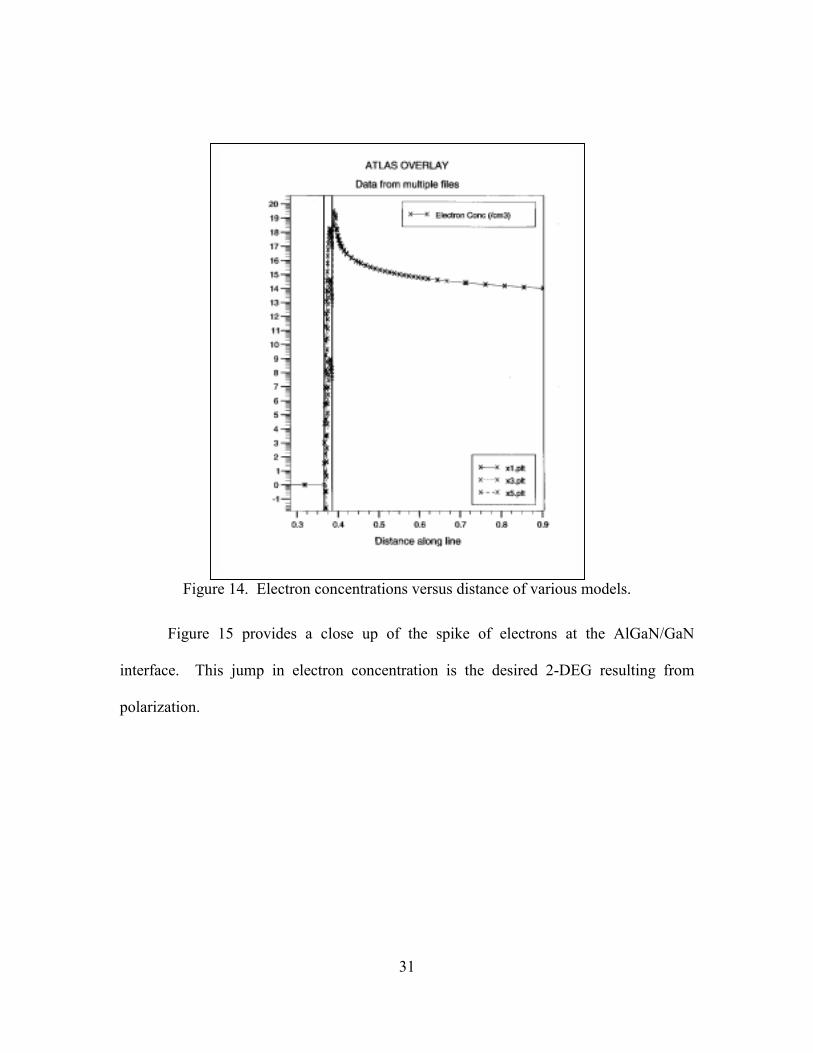
Figure 14. Electron concentrations versus distance of various models.
Figure 15 provides a close up of the spike of electrons at the AlGaN/GaN
interface. This jump in electron concentration is the desired 2-DEG resulting from
polarization.

32
Figure 15. Electron concentrations at the interface of various models.
As can be seen in Figure 15, the amount of charge in the channel is approximately
the same as the doping and what Ambacher predicts. This is the desired result of this
thesis. Figure 15 provides both the electron concentration and the doping profile so that
one can see that while the electron concentration exceeds the desired doping
concentration, it does so only in a very reduced area. Using Silvaco�s Integrate function
in TONYPLOT, these two areas were found to differ by less than 4%.
The following figures show the energy bands of the device, again looking at a
cutline from the gate through the AlGaN layer and into the GaN layer. They demonstrate
the expected shape for a HEMT device as seen back in Figure 4.

33
Figure 16. Conduction and valence band energy versus distance of various models.
Figure 16 shows the entire energy band diagram around the AlGaN layer while
Figure 17 shows the conduction band more closely. Once can see the expected trench or
quantum well that make the HEMT a unique transistor device. (Figures 12 through 17
all show the results from three models of different Aluminum mole fractions, as specified
in the lower right corner. The demonstrated Aluminum mole fractions are x = 0.1, 0.3,
and 0.5.)

34
Figure 17. Conduction band energy of various models (close up).
C. IV CURVES
The model was tested and compared with measured results by NRL [16]. The
model was run with a 0.3 Al mole fraction under different gate biases. Figure 18 displays
the results. The device was subjected to a drain bias ramped from 0.0 to 20.0 Volts with
gate biases of 0.0, -1.0, -3.0, and �5.0 Volts.

35
Figure 18. Simulated IV curves for AlGaN HEMT transistor.
NRL�s results on a real device are shown in Figure 19.
Figure 19. Measured IV curves for AlGaN HEMT transistor.
00.00010.00020.00030.00040.00050.00060.00070.00080.0009
0.0
2.5
5.0
7.5
10.0
12.5
15.0
17.5
20.0
Drain [V]
Dra
in [A
] gate bias 0.0 Vgate bias -1.0 Vgate bias -3.0 Vgate bias -5.0 V

36
The model IV curves have noticeable differences. While the real device peaks by
five volts on the drain, only the �5.0 gate bias case does so in the model. The real device
never surpasses about 0.0009 Amps while the model approaches 0.0012 Amps. The real
device curves (except the �5.0 volt case) begin to fall off around thirteen volts on the
drain, but the model drain current never fall off. This anomaly is expected to be caused
by heating effects for which the model does not account. Despite these differences, the
model curves and the real curves are roughly similar and hopefully show promise for
using the Silvaco model. Figure 20 shows the simulated and measured results overlaid
with the 0.0 V and the �5.0 V gate bias conditions.
Figure 20. Simulated and measured IV curves for AlGaN HEMT transistor.
00.00010.00020.00030.00040.00050.00060.00070.00080.0009
0.0
2.0
4.0
6.0
8.0
10.0
12.0
14.0
16.0
18.0
20.0
Drain bias
Am
ps
Sim gate 0Sim gate -5Meas gate 0Meas gate -5

37
IV. DISCUSSION
The above cutlines demonstrate that appropriate levels of electron sheet
concentrations have been achieved at the AlGaN-GaN interface. The model successfully
models the impact of various Aluminum mole fractions.
The IV curves demonstrate correspondence between the model and a real device.
Some investigation into the differences was conducted. The simulation�s slower rise to
peak current was thought to be due to leakage current moving through the substrate (not
in the 2-DEG channel beneath the AlGaN interface), however, a current flow analysis
eliminated that possibility. All current in the device is travelling through the 2-DEG
channel. Gate current leakage was also investigated but eliminated as the cause as it is
less than 1e-17 (virtual zero). NRL measured gate leakage in actual devices which
demonstrated greater leakage (though still negligible) than the simulations. Attempts
were made to increase carrier mobility and decrease saturation velocity without
satisfactory results. More than a dozen simulations using various mobilities and
saturation velocities were run without achieving the steep slope of the measured device
from 0.0 to 4.0 volts. A matching peak current of 0.00084 Amps was achieved. An
electron mobility of 9000 cm2/V-sec and electron velocity saturation of 1.1e7 cm/sec
were used based on work reported by Eastman in [18].
After exploring options in adjusting electron mobility and velocity saturation, one
of two results can be achieved: the steep current rise from 0.0 to 4.0 volts can be
matched (but peak current greatly exceeds desired levels), or the peak current can be
matched (but the current rise at lower voltages lags behind the desired levels).

38
Accordingly, other options can be investigated. The thickness of the 2-DEG is currently
0.01 microns. A thinner 2-DEG could be achieved with an adjusted model structure. A
structure with less substrate and more focussed meshing (grouping of points within the
structure where equilibrium equations are calculated by Silvaco software) would allow a
more refined 2-DEG. However, this approach might reduce the effectiveness of a model
which includes thermal effects. Without the substrate (sapphire or Silicon Carbide),
modeling a device under thermal conditions might suffer in accuracy.
Other means to attack the I-V curve discrepancies are available in Silvaco
Software. Some options not used in this work were the ability to model thermal effects,
interface effects, and quantum effects. Silvaco software has a program called GIGATM
which extends ATLASTM to account for lattice heat flow by implementing Wachutka�s
thermodynamic model. This program would probably assist the accurate modeling of
high field effects where the current begins to decrease, though its impact on the low field
problems is doubtful. ATLASTM has an INTERFACE statement that allows one to define
the interface charge density. This function might allow a simple method for defining the
2-DEG, but it would preclude the option of automating the density of the 2-DEG which
this project has achieved. The INTERFACE statement also modifies the surface
recombination velocity and thermionic emission which might not be desired. Quantum
effects can be addressed in Silvaco by including solution of Schrodinger�s equation
(which modifies the normally calculated density of states and carrier concentrations)
and/or including equations to correct carrier temperature through quantum potential.
The impact of these equations might have an adverse effect on accurate control of the 2-
DEG density.

39
Another issue to consider is the method of modeling the 2-DEG with doping. The
method used in this work is expected to be accurate since Silvaco software normally
reacts to doping by reducing electron mobility. Since this model takes manual control of
mobility, the result should be a device with the correct mobility and extra electrons at the
heterojunction. However, a better approach might be to take electrons from other areas in
the device. The software would have to move them to the interface and maintain the
appropriate level of concentration as predicted by Ambacher. This approach would
require some extensive work with Silvaco, as the software does not currently allow such
an option.

40
THIS PAGE INTENTIONALLY LEFT BLANK

41
VI. CONCLUSIONS AND RECOMMENDATIONS
A. CONCLUSIONS
PZ and spontaneous polarization effects are significant in GaN devices and can be
modeled with Silvaco Software. The desired density of current carriers has been related
to the mole fraction of Al in AlGaN. The equations of Ambacher et al. are readily
implemented by this model. The current versus voltage performance of the modeled
device approximates a measured device, however, it requires some treatment before it
will closely match actual device performance. Potential areas for correcting the
inaccuracies have been discussed.
B. RECOMMENDATIONS
Strenuous attempts to match real device performance could now be performed.
Silvaco Software has capabilities to incorporate thermal effects and Silicon Carbide
(instead of Sapphire) as a substrate. These are areas of current concern in device
fabrication which ONR and industry ought to be attracted to fund such work.
Silvaco Software has expressed interest to incorporate the PZ effect into the
BLAZE software module. This effort would aid Navy needs in developing new GaN
devices. Future thesis research can be conducted in cooperation with Silvaco to
incorporate this work into their software. Specifically, the AlGaN layer thickness and
mole fraction composition might be automatically updated from the structure file (to
eliminate the need to enter those values into the C-INTERPRETER code). Also the
Fermi level might be automatically updated and provided to the C-INTERPRETER
function rather than using equation 15.

42
Applying external stress to devices to optimize the 2-DEG created from the PZ
effect offers further enhancement of HEMT performance. UC Berkley has expressed an
interest in performing the experiments required to measure this phenomenon. The results
of such work could be incorporated into the Silvaco Software.
The modeling of the PZ effect is performed in a static fashion by this work. One
could investigate the possibility that a dynamic effect between applied voltage bias and
PZ effect occurs. If so, Silvaco may be able to incorporate such an effect to their
software.

43
LIST OF REFERENCES
1. Smith, M.C., Dunleavy, L.P., �Comparison of Solid State, MPM, and TWT Based Transmitters for Spaceborne Applications,� Proceedings of IEEE Southeastcon �98, pp. 256-259, April 23, 1998.
2. Gonzalez, Guillermo, Microwave Transistor Amplifiers: Analysis and Design, Prentice Hall, New Jersey, 1997, p. 81.
3. Pierret, Robert, Semiconductor Device Fundamentals, Addison-Wesley Publishing Company, Massachusetts, 1996, p. 526.
4. Burm, J., �General Remarks on GaN-based Transistors and Potential for High Temperature/Power Operation,� Jun 1998, Properties, Processing and Applications of Gallium Nitride and Related Semiconductors, INSPEC 1999, p. 569.
5. Jelenski, Andrzej, �Gallium Nitride--New Material for Microwave and Optoelectronics,� Microwaves and Radar, MIKON '98, 12th International Conference on , Vol. 4, 1998, pp. 147-158.
6. Takeuchi and Akasaki, �GaInN Quantum Wells: Piezoelectricity,� Feb 1998 Properties, Processing and Applications of Gallium Nitride and Related Semiconductors, INSPEC 1999, p. 525.
7. Asbeck, P.M., et al, �Piezoelectric Charge Densities in AlGaN/GaN HFETs,� ELECTRONIC LETTERS, 3 July 1997, Vol. 33, No.14, pp. 1230-1231.
8. Kittel, Charles, Introduction to Solid State Physics, 5th Edition, John Wiley & Sons, New York, NY, 1976.
9. Kasap, S.O., Principles of Electrical Engineering Materials and Devices, IRWIN, Chicago, IL, 1997.
10. Silvaco International, ATLAS User�s Manual, November 1998.
11. Haliday, Resnik, Walker, Fundamentals of Physics 5th Edition, John Wiley & Sons, New York, NY, 1997.
12. Leszczynski, M, et al, �Lattice Parameters of the Group III Nitrides,� Feb 1998 Properties, Processing and Applications of Gallium Nitride and Related Semiconductors, INSPEC 1999 p. 6-9.
13. Ambacher, O., et al, �Two Dimensional Electron Gases Induced by Spontaneous and Piezoelectric Polarization in Undoped and Doped AlGaN/GaN Heterostructures,� Journal of Applied Physics, Vol. 87, Number 1, January 1, 2000, p. 334-344.
14. Shur, Michael, Physics of Semiconductor Devices, Prentice Hall, Engelwood Cliffs, NJ, 1990.

44
15. Dimitrijev, Sima, Understanding Semiconductor Devices, Oxford University Press, New York, 2000.
16. Binari, S.C. et al, �Trapping Effects and Microwave Power Performance in AlGaN/GaN HEMTs,� unpublished report (expect to be published in Electron Device Letters, April 2001)
17. Mohney, S., �Schottky Barrier Contacts to GaN,� April 1998, Properties, Processing and Applications of Gallium Nitride and Related Semiconductors, INSPEC 1999, p. 496.
18. Eastman, L, �High Power, Broadband, Linear, Solid State Amplifier 1st Annual Report under MURI Contract No. N00014-96-1-1223� Sept. 1, 1996 � Aug. 31, 1997. http://www.iiiv.cornell.edu/www/schaff/muri/reports/fy97annual/ annual_report.html
45
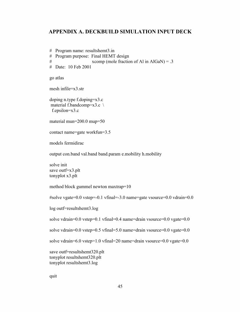
APPENDIX A. DECKBUILD SIMULATION INPUT DECK
# Program name: resultshemt3.in # Program purpose: Final HEMT design
# xcomp (mole fraction of Al in AlGaN) = .3 # Date: 10 Feb 2001 go atlas mesh infile=x3.str doping n.type f.doping=x3.c material f.bandcomp=x3.c \ f.epsilon=x3.c material mun=200.0 mup=50 contact name=gate workfun=3.5 models fermidirac output con.band val.band band.param e.mobility h.mobility solve init save outf=x3.plt tonyplot x3.plt method block gummel newton maxtrap=10 #solve vgate=0.0 vstep=-0.1 vfinal=-3.0 name=gate vsource=0.0 vdrain=0.0 log outf=resultshemt3.log solve vdrain=0.0 vstep=0.1 vfinal=0.4 name=drain vsource=0.0 vgate=0.0 solve vdrain=0.0 vstep=0.5 vfinal=5.0 name=drain vsource=0.0 vgate=0.0 solve vdrain=6.0 vstep=1.0 vfinal=20 name=drain vsource=0.0 vgate=0.0 save outf=resultshemt320.plt tonyplot resultshemt320.plt tonyplot resultshemt3.log
quit

46
THIS PAGE INTENTIONALLY LEFT BLANK

47
APPENDIX B. C-INTERPRETER FILE
#include <stdio.h> #include <stdlib.h> #include <math.h> #include <ctype.h> #include <malloc.h> #include <string.h> /* FILE NAME: x3.c*/ /* * Composition and temperature dependent electron saturation velocity * Statement: MATERIAL * Parameter: F.VSATN = */ /* electron saturation velocity */ int vsatn(double xcomp,double ycomp,double temp,double *vsn,double *dvsn) { return(0); /* 0 - ok */ } /* * Composition and temperature dependent hole saturation velocity * Statement: MATERIAL * Parameter: F.VSATP */ /* hole saturation velocity */ int vsatp(double xcomp,double ycomp,double temp,double *vsn,double *dvsn) { return(0); /* 0 - ok */ } /* * Electron velocity saturation model. * Statement: MATERIAL * Parameter: F.MUNSAT */ /* electron velocity saturation */ int munsat(double e,double v,double mu0,double *mu,double *dmde) { return(0); /* 0 - ok */ } /* electron velocity saturation */

48
/* * Hole velocity saturation model. * Statement: MATERIAL * Parameter: F.MUPSAT */ int mupsat(double e,double v,double mu0,double *mu,double *dmde) { return(0); /* 0 - ok */ } /* position dependent doping */ /* * Position dependent net doping. * Statement: DOPING * Parameter: F.DOPING */ int doping(double x,double y,double *nnet) { /*Ambacher*/ double xAct, x2, e, epsilon0, dalgan, Efermi, fib, Eg, Eg0, deltaEC; double epsilonx, r, a0, agan, c13, c33, e31AlN, e31GaN, e33AlN, e33GaN; double e31, e33, Ppe, Psp, Ppe0, Psp0, sigma, ns; double nn, nn1, nn2, nn3; xAct=0.3; /*mole fraction of Al in AlGaN (must be adjusted manually)*/ x2=xAct; e=1.60218e-19; /*[C] charge of an electron*/ epsilon0=8.8542e-12; /*[C/VM] permittivity of free space*/ dalgan=200e-10; Efermi=2.1917*x2-0.102967-7*x2*x2*x2*x2*x2*x2; /* [CV] Fermi level
wrt GaN conduct. band energy*/ fib=1.3*x2+.84; /*[CV--(eV)] Gate Schottky barrier (work function?)*/ Eg=x2*6.13+(1-x2)*3.42-x2*(1-x2); /*[CV] AlGaN bandgap (x2 = Al mole
fraction)*/ Eg0=3.42; /*[CV] GaN bandgap*/ deltaEC=0.7*(Eg-Eg0); /*[CV] band offset*/ epsilonx=-.3*x2+10.4; /*[] relative permittivity*/ r; if (x2<=0.38) r=0.0; /*[] degree of relaxation*/

49
if (x2>0.38) if (x2<=0.67) r=3.5*x2-1.33; if (x2>0.67) r=1.0; a0=(-0.077*x2+3.189)*1.e-10; /*[m] AlGaN lattice constant*/ agan=3.189e-10; /*[m] GaN lattice constant*/ c13=(5*x2+103); /*[GPa] AlGaN elastic coefficients*/ c33=(-32*x2+405); e31AlN=-.6; /*[C/m^2] PZ coefficients*/ e31GaN=-.49; e33AlN=1.46; e33GaN=.73; e31=(e31AlN-e31GaN)*x2+e31GaN; e33=(e33AlN-e33GaN)*x2+e33GaN; /*double e31AlN=-.58;*/ /* alt. PZ coefficients (not used)*/ /*double e31GaN=-.36;*/ /*but mentioned in Ambacher.*/ /*double e33AlN=1.55;*/ /*double e33GaN=1.0;*/ /*double e312=(e31AlN-e31GaN)*x2+e31GaN;*/ /*double e332=(e33AlN-e33GaN)*x2+e33GaN;*/ /*double e31AlN=-.38;*/ /*double e31GaN=-.32;*/ /*double e33AlN=1.29;*/ /*double e33GaN=.63;*/ /*double e313=(e31AlN-e31GaN)*x2+e31GaN;*/ /*double e333=(e33AlN-e33GaN)*x2+e33GaN;*/ Ppe=2*(r-1)*((a0-agan)/a0)*(e31-e33*(c13/c33)); /*PZ polarization*/ Psp=(-0.052*x2-0.029); /*Spontaneous polarization*/

50
x2=0.0; e31=(e31AlN-e31GaN)*x2+e31GaN; /*Resetting constants & coeff.*/ e33=(e33AlN-e33GaN)*x2+e33GaN; /*for GaN*/ a0=(-0.077*x2+3.189)*1.e-10; c13=(5*x2+103); c33=(-32*x2+405); r=0.0; Ppe0=2*(r-1)*((a0-agan)/a0)*(e31-e33*(c13/c33)); /*PZ polarization*/ Psp0=(-0.052*x2-0.029); /*Spontaneous polarization*/ x2=xAct; sigma=(Ppe0+Psp0)-(Ppe+Psp); /*sheet charge per m^2*/ sigma=sigma/1.e4; /*per cm^2*/ /*electron sheet concentration*/ ns=sigma/e-(epsilon0*epsilonx/(dalgan*e))*(fib+Efermi-deltaEC)/1.e4; /*e311 Constants measured differently by various researchers*/ /*e312 provided by Ambacher.*/ /*e313 actually used above*/ /*e331*/ /*e332*/ /*e333 actually used above*/ /*Ambacher*/ nn1 = 1.e5; nn2 = 5.e18; nn3 = ns*(1.e6); //Sheet charge is spread over 0.01 microns, so nn = nn1; //ns [n/cm^2] is multiplied by 1/10^-6 [cm^-1] //in order to translate to [n/cm^3] which //ATLAS requires. if (x>1.6 && x<3.7) { if (y>=-0.02 && y<-0.0025) nn=nn2; if (y>=0 && y<=0.01) nn=nn3; }

51
*(nnet) = nn; return(0); /* 0 - ok */ } /* band parameters */ /* * Temperature and composition dependent band parameters * Statement: MATERIAL * Parameter: F.BANDCOMP * Note: This function can only be used with BLAZE. */ int bandcomp(double xcomp,double ycomp,double temp,double *eg,double
*chi,double *nc,double *nv,double *degdt) { double egr, chir, ncr, nvr; egr = 3.39+xcomp*2.81; chir = 2.7-xcomp*2.0; ncr = (1.79+xcomp*2.63)*1.e18; nvr = (3.31+xcomp*3.45)*1.e18; *(eg) = egr; *(chi) = chir; *(nc) = ncr; *(nv) = nvr; return(0); /* 0 - ok */ } /* electron mobility */ /* * Composition, temperature and doping dependent electron mobility * Statement: MATERIAL * Parameter: F.CONMUN */ int conmun(double xcomp,double ycomp,double temp,double ntot,double *mun) { return(0); /* 0 - ok */ } /* hole mobility */

52
/* * Composition, temperature and doping dependent hole mobility * Statement: MATERIAL * Parameter: F.CONMUP */ int conmup(double xcomp,double ycomp,double temp,double ntot,double *mup) { return(0); /* 0 - ok */ } /* relative permittivity */ /* * Composition and temperature dependent permittivity. * Statement: MATERIAL * Parameter: F.EPSILON */ int epsilon(double xcomp,double ycomp,double temp,double *eps) { double epsr; epsr = 9.0-xcomp*0.5; *(eps) = epsr; return(0); /* 0 - ok */ } /* interface fixed charge */ /* * Interface fixed charge as a function of position. * Statement: INTERFACE * Parameter: F.QF */ int int_fixed_charge(double x,double y,double *fixed) { return(0); } /* device degradation interface acceptor traps */ /* * Interface acceptor trap density as a function of location * Statement: DEGREDATIONPARAM * Parameter: F.NTA */

53
int devdeg_nta(double x,double y,double *nta) { return(0); } /* device degradation interface donor traps */ /* * Interface donor trap density as a function of location * Statement: DEGREDATIONPARAM * Parameter: F.NTD */ int devdeg_ntd(double x,double y,double *ntd) { return(0); } /* device degradation electron capture xsect */ /* * Interface electron capture cross section * Statement: DEGREDATIONPARAM * Parameter: F.SIGMAE */ int devdeg_sigmae(double x,double y,double *sigmae) { return(0); } /* device degradation hole capture xsection */ /* * Interface hole capture cross section * Statement: DEGREDATIONPARAM * Parameter: F.SIGMAH */ int devdeg_sigmah(double x,double y,double *sigmah) { return(0); } /* interface acceptor traps */ /* * Interface acceptor trap density as a function of location * Statement: INTTRAP (ACCEPTOR) * Parameter: F.DENSITY */ int int_acc_trap(double x,double y,double *density) {

54
return(0); } /* interface donor traps */ /* * Interface donor trap density as a function of location * Statement: INTTRAP (DONOR) * Parameter: F.DENSITY */ int int_don_trap(double x,double y,double *density) { return(0); } /* * Interface donor trap density vs position * Statement: INTTRAP * Parameter: F.INTDONOR */ int intdonor(double x,double y,double energy,double *density,double
*ncross,double *pcross,double *nlife,double *plife,double *gd) { return(0); } /* * Interface acceptor trap density vs position * Statement: INTTRAP * Parameter: F.INTACCEPTO */ int intacceptor(double x,double y,double energy,double *density,double
*ncross,double *pcross,double *nlife,double *plife,double *ga) { return(0); }

55
INITIAL DISTRIBUTION LIST 1. Defense Technical Information Center ................................................................... 2
8725 John J. Kingman Road, Suite 0944 Ft. Belvoir, VA 22060-6218
2. Dudley Knox Library .............................................................................................. 2 Naval Postgraduate School 411 Dyer Road Monterey, CA 93943-5101
3. Engineering and Technology Curricular Office, Code 34���������...1 Naval Postgraduate School Monterey, CA 93943-5109
4. Chairman, Code EC������������������������.1 Department of Electrical and Computer Engineering Naval Postgraduate School
Monterey, CA 93943-5121 5. Prof. Todd R. Weatherford, Code EC/Wt����������������3
Department of Electrical and Computer Engineering Naval Postgraduate School
Monterey, CA 93943-5121
6. Dr. Harry Dietrich�������������������������2 Code 6856 Naval Research Laboratory Washington D.C. 20375
7. LT Karl P. Eimers, USN����������������������..3
P.O. Box K St. Maries, ID 83861


![A Survey of Modeling and Control of Piezoelectric Actuatorsfile.scirp.org/pdf/MME_2013022713035446.pdf · A Survey of Modeling and Control of Piezoelectric ... ity [19]. For improvement,](https://img.pdfslide.us/doc/110x75/5aa360e57f8b9a46238e4273/a-survey-of-modeling-and-control-of-piezoelectric-survey-of-modeling-and-control.jpg)