Embed Size (px)
Citation preview
Logarithmic Circuits
© John Knight
Dig Cir p. 99 Revised; October 23, 2003
Logarithmic CircuitsBinary Up Counter
1T
C
“Q”
1
CLK
“T”
Q0
Q1
Q2
Q3
1T
C1
CLK
1T
C1
1T
C1
1T
C1
Q0Q1Q2Q3
4-bit binary counter
T3 T2 T1
TC=T4
T0
The circles show how
defined by ANDs:T1 = Q0T2 = Q1Q0T3 = Q2Q1Q0TC = Q3Q2Q1Q0
the toggle signals are
Toggle Flip Flop
If T=1, toggle output QIf T=0, hold old Q
@(posedge clk)
Simplest Counter Circuit Uses T Flip-Flops
0 1
0
0
0
0
0
0
0
0
1
1
0
0
1
0
0
1
0
1
0
1
0
0
0
1
1
1
0
1
0
1
0
0
1
1
0
0
0
0
0
1
0
Notice the ripple carry. This limits the speed of the counter.
Propagation Delay
1
TC = Teminal Count
Slide 50
Carleton University © John KnightDigital Circuits p. 100 Revised; October 23, 2003
Logarithmic Circuits Binary Counters
Binary CountersThe simplest counters use toggle flip-flops. These are made from D flip-flopsas shown.
This is why many circuits of counters show an XOR gate and an AND gate foreach flip-flop.
The AND gates, drawn on top of the waveforms, show how the flip-flops toggle whenever all the precedingflip-flops are one.
Counter Speed
Note that for long counters the chain of AND gates will get very long and will limit the speed of the counter. Fora 32 bit counter, the clock speed must allow propagation through 31 AND gates plus the clock-to-output andsetup times of a flip-flop.
1DC1
D QT
T=0� D=QoldT=1� D=~Qold
Comment on Slide 50
Logarithmic Circuits
© John Knight
Dig Cir p. 101 Revised; October 23, 2003
Logarithmic Carry in a Binary Counter
Ripple Carry Circuit Using T Flip-Flops
Logarithmic Carry Circuit Using T Flip-Flops
1T
C1
1T
C1
1T
C1
1T
C1
Q4Q5Q6Q7
8-bit binary counter using a ripple carry
T7 T6 T5
T8
T41T
C1
CLK
1T
C1
1T
C1
1T
C1
Q0Q1Q2Q3T3 T2 T1 T0
012456 37
Delay is N-1 (7), AND gate delays
1T
C1
1T
C1
1T
C1
1T
C1
Q4Q5Q6Q7
8-bit binary counter using logarithmic carry
T7 T6 T5
T8
T41T
C1CLK
1T
C1
1T
C1
1T
C1Q0
Q1Q2Q3T3 T2 T1 T0
1111 2
2
2
2
3
333
Delay is log2(N) = 3, AND gate delaysbut watchthe fanout
Level number
Slide 51
Carleton University © John KnightDigital Circuits p. 102 Revised; October 23, 2003
Logarithmic Circuits Logarithmic Ripple-Carry Counter
Comment on Slide 51
Logarithmic Ripple-Carry CounterBy placing a buffer as shown, the end-to-end carry need only pass through 2log2(N) gates.
Counter SpeedIn the ripple-carry circuit.
The time between a clock edge and a stable outbut from TC is:TCHQV for Q0 + (Tpd for 7 AND gates).
Ignoring the flip-flop delay, this is a delay proportional to N-1, for N flip-flops.
The fanout also effects the delay. Here all fanouts are 2.
In the logarithmic carry circuit.
The slowest carry, TC, must go from:
a. The clock input to Q0
b. Q0 through a 1st level AND (green with a “1” in side).
c. through a 2nd level AND gate (red with a “2” inside).
d. through a 3rd level AND gate (blue with a “3” inside).
For N flip-flops this delay is proportional to log2(N).
However the fanouts increase the delay. The largest fanout is N/2 + 1, (five for N=8).
Logarithmic Circuits
© John Knight
Dig Cir p. 103 Revised; October 23, 2003
Logarithmic Carry for TC for a 16-Bit Counter
C0
C1
C10=T2
C2
C3
C32
C10
C32
C30=T4
C4
C5
C54
C6
C7
C76
C54
C76
C74
C8
C9
C98
C10
C11
C1514
C1312
C1512
C98
C30
C74
C70=T8
C70
C118
C150=T16
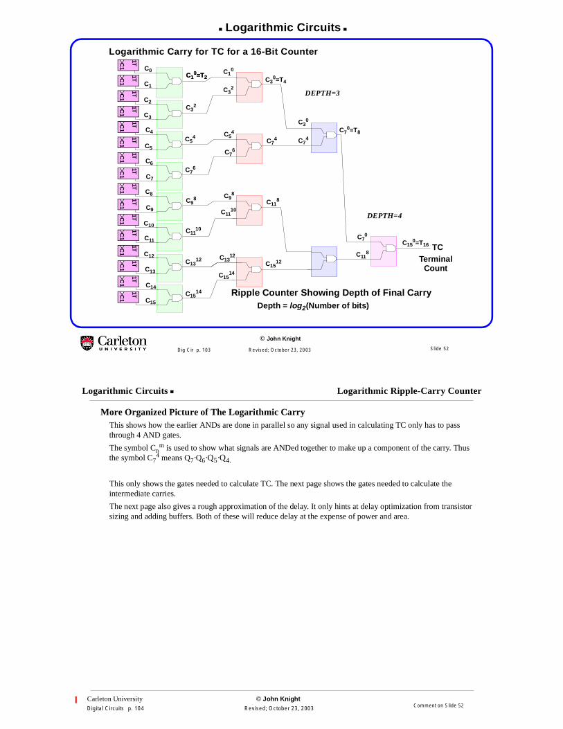
Ripple Counter Showing Depth of Final CarryDepth = log2(Number of bits)
DEPTH=4
DEPTH=3
C13
C12
C15
C14
C1110
C1110
C1312
C1514
C118
1TC1
1TC1
1TC1
1TC1
1TC1
1TC1
1TC1
1TC1
1TC1
1TC1
1TC1
1TC1
1TC1
1TC1
1TC1
1TC1
C10=T2
TCTerminal
Count
Slide 52
Carleton University © John KnightDigital Circuits p. 104 Revised; October 23, 2003
Logarithmic Circuits Logarithmic Ripple-Carry Counter
Comment on Slide 52
More Organized Picture of The Logarithmic CarryThis shows how the earlier ANDs are done in parallel so any signal used in calculating TC only has to passthrough 4 AND gates.
The symbol Cnm is used to show what signals are ANDed together to make up a component of the carry. Thus
the symbol C74 means Q7·Q6·Q5·Q4.
This only shows the gates needed to calculate TC. The next page shows the gates needed to calculate theintermediate carries.
The next page also gives a rough approximation of the delay. It only hints at delay optimization from transistorsizing and adding buffers. Both of these will reduce delay at the expense of power and area.
Logarithmic Circuits
© John Knight
Dig Cir p. 105 Revised; October 23, 2003
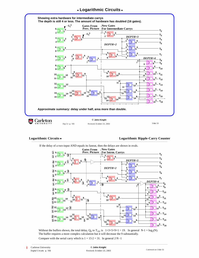
Showing extra hardware for intermediate carrysThe depth is still 4 or less. The amount of hardware has doubled (16 gates).
Approximate summary: delay under half, area more than double.
1100
3322
55
44
7766
9 988
1111
1010
301
0
32
745
4
76
1189
8
1110
703
0
74
110
118
201
0
2
403
0
4
503
0
54
664 6
030
64
54
807
0
8
90
98
10 108 10
010
898
T2
T3
T4
T5
T6
T7
T8T9
T10
T11
T12
Gates FromPrev. Picture
New GatesFor Intermediate Carrys
DEPTH=4
DEPTH=3
DEPTH=2
1313
1212
1515
141415
1413
12
1512 15
8118
1512
12811
8
12
138
1312
148
14 141213
12
120 T13
130 T14
140 T15
150 T16
C10
C30
Slide 53
Carleton University © John KnightDigital Circuits p. 106 Revised; October 23, 2003
Logarithmic Circuits Logarithmic Ripple-Carry Counter
Comment on Slide 53
If the delay of a two-input AND equals its fanout, then the delays are shown in ovals.
Without the buffers shown, the total delay, Q0 to T16, is 1+3+5+9+1 = 19. In general N-1 + log2(N).The buffer requires a more complex calculation but it will decrease the 9 substantially.
Compare with the serial carry which is 1 + 15·2 = 31. In general 2·N -1
11
00
3322
5544
77
66
9 988
1111
1010
301
0
32
745
4
76
1189
8
1110
703
0
74
110
118
201
0
2
403
0
4
503
0
54
66
4 603
0
64
54
807
0
8
90
98
10 108 10
010
898
T2
T3
T4
T5
T6
T7
T8T9
T10
T11
T12
Gates FromPrev. Picture
New GatesFor Intrm. Carrys
DEPTH=4
DEPTH=3
DEPTH=2
1313
1212
1515
1414
1514
1312
1512 15
8118
1512
12811
8
12
138
1312
148
14 141213
12
120 T13
130 T14
140 T15
150 T16
3
5
3
1
11 9
3
3
5
1
2
2
2
2
11
1
2
1
1
21
1
21
1
Addition
© John Knight
Dig Cir p. 107 Revised; October 23, 2003
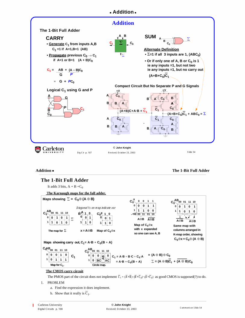
AdditionThe 1-Bit Full Adder
C1 = AB +PG
�
C0C1
BA
�
= G + PC0
C1 =1 if A=1,B=1 (AB)
A
BC0
C1
G
P
CARRY
ABB
C0A
(A+B)C+A·B = C1
+V
ABB
C0A
A
C0B
�
(A + B)C0
• Generate C1 from inputs A,B
• Propagate previous C0 → C1if A=1 or B=1 (A + B)C0
SUM
• Σ=1 if all 3 inputs are 1, (ABC0)
• Or if only one of A, B or C0 is 1ie any inputs =1, but not two
(A+B+C0)C1
AB
C0
C0
A
B
C1
AB
C0
C0
A
B
C1
A
+VCompact Circuit But No Separate P and G Signals
ie any inputs =1, but no carry out
(A+B+C0)C1 + ABC0 = Σ
Alternate Definition
Logical C1 using G and P
Slide 54
Carleton University © John KnightDigital Circuits p. 108 Revised; October 23, 2003
Addition The 1-Bit Full Adder
Comment on Slide 54
The 1-Bit Full AdderIt adds 3 bits, A + B +C0
The Karnaugh maps for the full adder.
The CMOS carry circuit
The PMOS part of the circuit does not implement C1 = (A+B)· (B+C0)· (A+C0) as good CMOS is supposed(?) to do.
1. PROBLEM
a. Find the expression it does implement.
b. Show that it really is C1.
110
1
00 01 11 10
0
1
AB
0
AC
00
0 BC
00 01 11 10
0
1
AB
AB
0
1 00�
C1 = A·B + B·C + C0·A
= A·B + C0(B + A)
Maps showing carry out, C1= A·B + C0(B + A)
Circle map.
000
0
00 01 11 10
0
1
AB
1
1 11C1
Diagonal 1s on map indicate xor
� = (A ⊕ B)CI + (A ⊕ B)C0
= (A ⊕ B) ⊕ C0
BA0
1
1 00
0
1
1
C0
C0C0
C0x0
1
1 00
0
1
1
100
1
0 0 1 1
0
1
x
1
0 01
C0
A⊕BA⊕B
00 11 01 10AB
110
1
00 01 11 10
0
1
AB
0
1 00
C0
A⊕BA⊕B
The map for Σ x = A⊕B Map of C0⊕x
Map of C0⊕xwith x expandedso one can see A, B
Same map withcolumns arranged in
K-map order, showing
C0⊕x = C0⊕ (A ⊕ B)
Maps showing � = C0⊕ (A ⊕ B)
Map for C1.
Addition
© John Knight
Dig Cir p. 109 Revised; October 23, 2003
The 4-Bit Adder
Σ1
C1C2
B1A1
�
� = (A ⊕ B) ⊕ C0 A
B
A
C0B
�
Σ0
C0C1
B0A0
�
Σ3
C3C4
B3A3
�
Σ2
C2C3
B2A2
�
G3P3
Σ2
C2
B2A2
�
Σ3
B3A3
G2P2
G4P4
G1P1
Σ0
C0
B0A0
�
Σ1
C1
B1A1
�C3�
C = G + PC0
GPC
C0
Generate carry; G
Propagate carry; P
Ripple Carry Using Propagate and Generate
C0C4
Ripple-Carry Adder
Basic Adder Blocks
Longest PathG and P are independent of C �
Slide 55
Carleton University © John KnightDigital Circuits p. 110 Revised; October 23, 2003
Addition The 1-Bit Full Adder
Comment on Slide 55
2. PROBLEM
Show that the PMOS part of the full adder on Slide 54, implements the complement of the NMOS part.Hint: plot the PMOS function on a Karnaugh map. Then invert each square on the map to get the complement ofThe PMOS function, and check that it matches the NMOS map.
3.• PROBLEM
Some books define P=A⊕B. Show what this does to the C1 and � functions.What advantage does it have, i.e. smaller, faster, less power.
Solution:
The alternate P is generated for free because it is needed in the sum, thus saving an OR gate in each block.However the XOR takes more time to calculate, so the Ps will be delayed.Some circuits,. like the carry-bypass adder, demand that P=XOR.
Addition
© John Knight
Dig Cir p. 111 Revised; October 23, 2003
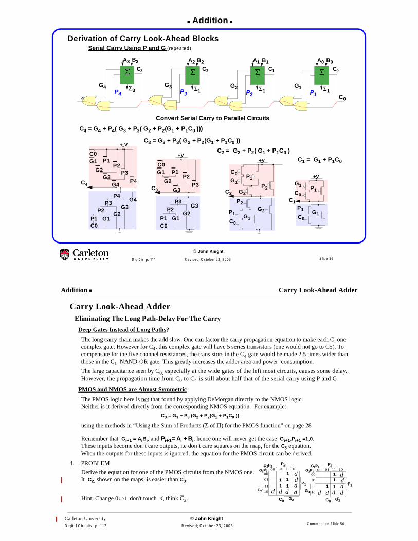
Derivation of Carry Look-Ahead Blocks
G3P3
C2
G2P2
G4P4
G1P1
C0C1C3
Serial Carry Using P and G (repeated)
C04
C4 = G4 + P4( G3 + P3( G2 + P2(G1 + P1C0 )))
C2 = G2 + P2( G1 + P1C0 )
C3 = G3 + P3( G2 + P2(G1 + P1C0 ))
C1 = G1 + P1C0
C0
P2
G1
G2
P1
+V
C2 C0
G1 P1
C1
+V
C0
G2P1
P2
G1
C0
C0
P1 G1G1P1
P2G2
P3G3
P4G4
C0P1G1
G2P2
G3P3
G4P4
+ V
C4
C0G1P1
P2G2
P3G3
C0P1G1
G2P2
G3P3
+V
C3
Σ3
B3A3
�
Σ1
B2A2
�
Σ1
B1A1
�
Σ1
B0A0
�
Convert Serial Carry to Parallel Circuits
Slide 56
Carleton University © John KnightDigital Circuits p. 112 Revised; October 23, 2003
Addition Carry Look-Ahead Adder
Comment on Slide 56
Carry Look-Ahead AdderEliminating The Long Path-Delay For The Carry
Deep Gates Instead of Long Paths?
The long carry chain makes the add slow. One can factor the carry propagation equation to make each Ci onecomplex gate. However for C4, this complex gate will have 5 series transistors (one would not go to C5). Tocompensate for the five channel resistances, the transistors in the C4 gate would be made 2.5 times wider thanthose in the C1 NAND-OR gate. This greatly increases the adder area and power consumption.
The large capacitance seen by C0, especially at the wide gates of the left most circuits, causes some delay.However, the propagation time from C0 to C4 is still about half that of the serial carry using P and G.
PMOS and NMOS are Almost Symmetric
The PMOS logic here is not that found by applying DeMorgan directly to the NMOS logic.Neither is it derived directly from the corresponding NMOS equation. For example:
C3 = G3 + P3 (G2 + P2(G1 + P1C0 ))
using the methods in “Using the Sum of Products (Σ of Π) for the PMOS function” on page 28
Remember that Gi+1 = AiBi, and Pi+1= Ai + Bi, hence one will never get the case Gi+1,Pi+1 =1,0.These inputs become don’t care outputs, i.e don’t care squares on the map, for the C3 equation.When the outputs for these inputs is ignored, the equation for the PMOS circuit can be derived.
4. PROBLEM
Derive the equation for one of the PMOS circuits from the NMOS one.It C2, shown on the maps, is easier than C3.
Hint: Change 0↔1, don't touch d, think C2.
1
d
P1
G1
P2
G2
d d
00
01
11
10
00 01 11 10G1P1
G2P2
1 d
d
d1
1d
C0
1
P1
G1
P2
G2
1
d
00
01
11
10
G2P2
1
d d
d1
1
d
C0
00 01 11 10G1P1d
d
Addition
© John Knight
Dig Cir p. 113 Revised; October 23, 2003
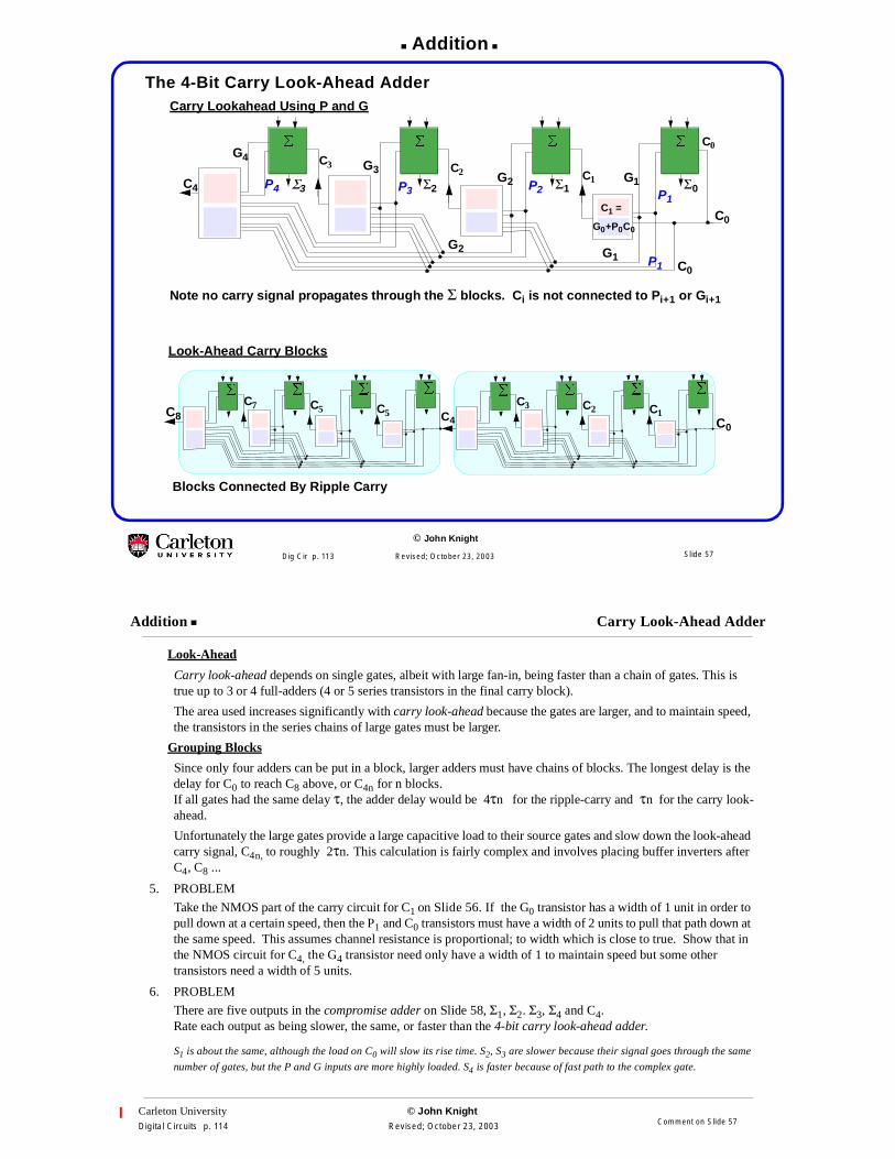
The 4-Bit Carry Look-Ahead Adder
G3
P3Σ3G2 P2
G4
P4G1
P1
C3
�
Carry Lookahead Using P and G
C0
C4 Σ1C1
�
Σ0
C0�
Σ2
C2
�
P1G1
G2
C1 =
G0+P0C0
C7
�
C8C5
� �
C5
�C3
�
C0C4
C1
� �
C2
�
Look-Ahead Carry Blocks
C0
Blocks Connected By Ripple Carry
Note no carry signal propagates through the Σ blocks. Ci is not connected to Pi+1 or Gi+1
Slide 57
Carleton University © John KnightDigital Circuits p. 114 Revised; October 23, 2003
Addition Carry Look-Ahead Adder
Comment on Slide 57
Look-Ahead
Carry look-ahead depends on single gates, albeit with large fan-in, being faster than a chain of gates. This istrue up to 3 or 4 full-adders (4 or 5 series transistors in the final carry block).
The area used increases significantly with carry look-ahead because the gates are larger, and to maintain speed,the transistors in the series chains of large gates must be larger.
Grouping Blocks
Since only four adders can be put in a block, larger adders must have chains of blocks. The longest delay is thedelay for C0 to reach C8 above, or C4n for n blocks.If all gates had the same delay τ, the adder delay would be 4τn for the ripple-carry and τn for the carry look-ahead.
Unfortunately the large gates provide a large capacitive load to their source gates and slow down the look-aheadcarry signal, C4n, to roughly 2τn. This calculation is fairly complex and involves placing buffer inverters afterC4, C8 ...
5. PROBLEM
Take the NMOS part of the carry circuit for C1 on Slide 56. If the G0 transistor has a width of 1 unit in order topull down at a certain speed, then the P1 and C0 transistors must have a width of 2 units to pull that path down atthe same speed. This assumes channel resistance is proportional; to width which is close to true. Show that inthe NMOS circuit for C4, the G4 transistor need only have a width of 1 to maintain speed but some othertransistors need a width of 5 units.
6. PROBLEM
There are five outputs in the compromise adder on Slide 58, Σ1, Σ2. Σ3, Σ4 and C4.Rate each output as being slower, the same, or faster than the 4-bit carry look-ahead adder.
S1 is about the same, although the load on C0 will slow its rise time. S2, S3 are slower because their signal goes through the same
number of gates, but the P and G inputs are more highly loaded. S4 is faster because of fast path to the complex gate.
Addition
© John Knight
Dig Cir p. 115 Revised; October 23, 2003
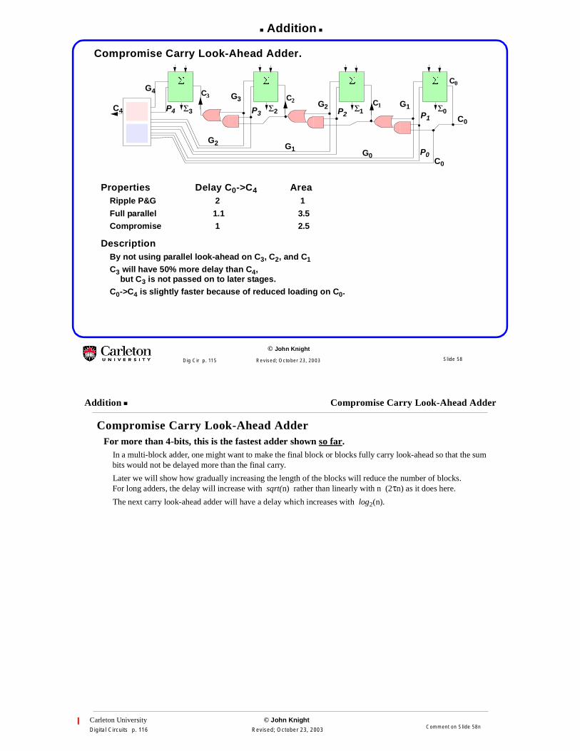
Compromise Carry Look-Ahead Adder.
Properties Delay C0->C4 AreaRipple P&G 2 1
Full parallel 1.1 3.5Compromise 1 2.5
DescriptionBy not using parallel look-ahead on C3, C2, and C1
C3 will have 50% more delay than C4,but C3 is not passed on to later stages.
C0->C4 is slightly faster because of reduced loading on C0.
G3
P3Σ3
G2P2
G4
P4G1
P1
C3
�
C0
C4 Σ1C1
�
Σ0
C0�
Σ2
C2
�
P0G0G1
G2
C0
Slide 58
Carleton University © John KnightDigital Circuits p. 116 Revised; October 23, 2003
Addition Compromise Carry Look-Ahead Adder
Compromise Carry Look-Ahead AdderFor more than 4-bits, this is the fastest adder shown so far.
In a multi-block adder, one might want to make the final block or blocks fully carry look-ahead so that the sumbits would not be delayed more than the final carry.
Later we will show how gradually increasing the length of the blocks will reduce the number of blocks.For long adders, the delay will increase with sqrt(n) rather than linearly with n (2τn) as it does here.
The next carry look-ahead adder will have a delay which increases with log2(n).
Comment on Slide 58n
Addition
© John Knight
Dig Cir p. 117 Revised; October 23, 2003
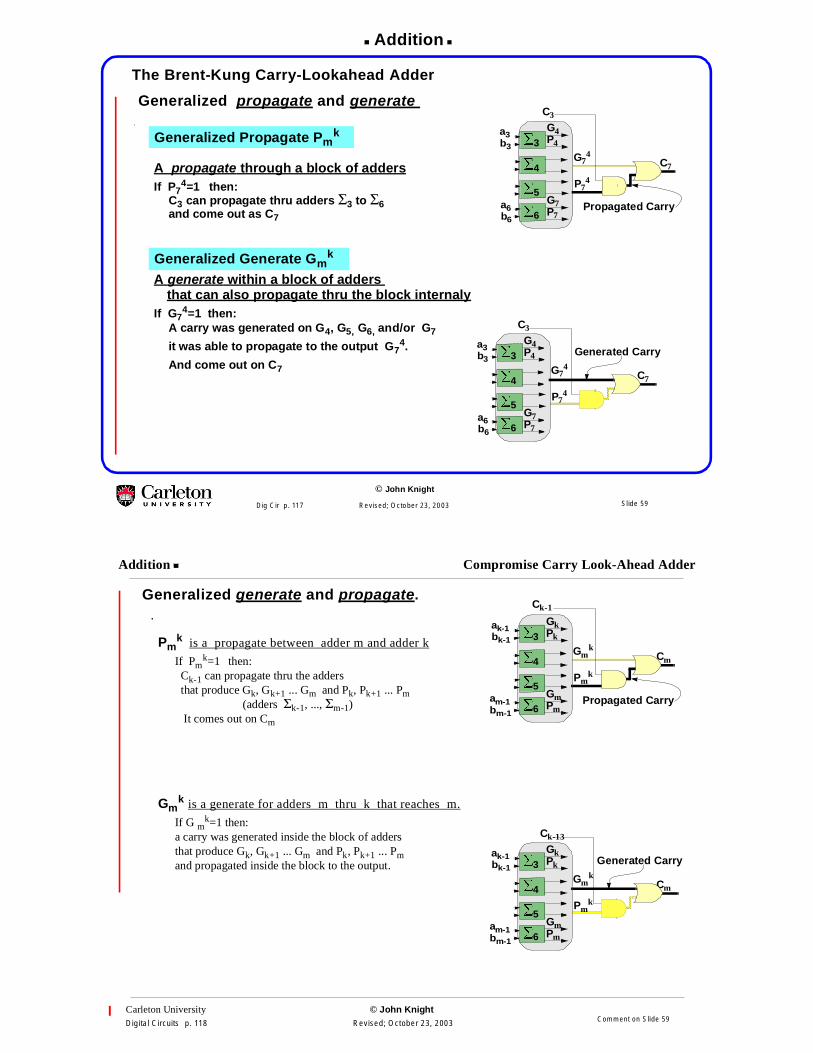
The Brent-Kung Carry-Lookahead Adder
Generalized propagate and generate
A propagate through a block of addersIf P7
4=1 then:C3 can propagate thru adders Σ3 to Σ6and come out as C7
A generate within a block of addersthat can also propagate thru the block internaly
If G74=1 then:
A carry was generated on G4, G5, G6, and/or G7
it was able to propagate to the output G74.
And come out on C7
�6
�5
�4
�3
C7
C3
P74
G74
Propagated Carry
b3
a3
b6
a6
G4P4
G7P7
Generalized Propagate Pmk
Generalized Generate Gmk
�6
�5
�4
�3
C7
C3
P74
G74
Generated Carryb3
a3
b6
a6
G4P4
G7P7
Slide 59
Carleton University © John KnightDigital Circuits p. 118 Revised; October 23, 2003
Addition Compromise Carry Look-Ahead Adder
Generalized generate and propagate.
Pmk is a propagate between adder m and adder k
If Pmk=1 then:
Ck-1 can propagate thru the addersthat produce Gk, Gk+1 ... Gm and Pk, Pk+1 ... Pm
(adders Σk-1, ..., Σm-1)It comes out on Cm
Gmk is a generate for adders m thru k that reaches m.
If G mk=1 then:
a carry was generated inside the block of addersthat produce Gk, Gk+1 ... Gm and Pk, Pk+1 ... Pmand propagated inside the block to the output.
�6
�5
�4
�3
Cm
Ck-1
Pmk
Gmk
Propagated Carry
bk-1
ak-1
bm-1
am-1
GkPk
GmPm
�6
�5
�4
�3
Cm
Ck-13
Pmk
Gmk
Generated Carrybk-1
ak-1
bm-1
am-1
GkPk
GmPm
Comment on Slide 59
Addition
© John Knight
Dig Cir p. 119 Revised; October 23, 2003
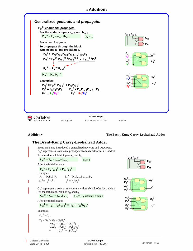
Generalized generate and propagate.
Pmk composite propagate.
For the adder’s inputs am-1 and bm-1
For other P signalsTo propagate through the blockOne needs all the propagates.
Examples:
Pmk = Pm
m Pm-1k = PmPm-1
k
P52 = P5P4P3P2 Pm
0 = PmPm-1Pm-2....P0
P53 = P5
5P43 P5
3 = P54P3
3
am-1bm-1Gm
Pm
G43
P55
G55
P53
P43 G5
3
G33
P54
G54
P53
P33 G5
3
Pmm = Pm = am-1+bm-1, P0 = 1
Pmk = PmPm-1Pm-2Pm-3 . . . Pk+1Pk
Pmk = Pm
m Pm-1m-1Pm-2
m-2 . . . Pk-1k-1Pk
k
Pmk = Pm
m Pm-1k
Pmk = Pm
j Pj-1k
Slide 60
Carleton University © John KnightDigital Circuits p. 120 Revised; October 23, 2003
Addition The Brent-Kung Carry-Lookahead Adder
The Brent-Kung Carry-Lookahead AdderBrent and Kung introduced a generalized generate and propagate.Pm
k represents a composite propagate from a block of m-k+1 adders.
For the adder’s initial inputs am and bm
After the initial inputs:-
Examples:P5
2 = P5P4P3P2 Pm0 = PmPm-1Pm-2....P0
P50 = P5
5P40 , P5
0 = P54P3
0
Gmk represents a composite generate within a block of m-k+1 adders.
For the initial adder inputs am and bm
After the initial inputs:-
Examples:
Gm0 =Cm
C5 = G50= G5 + P5G4
0
= G5 + P5(G4+ P4G30)
= (G5 + P5G4) + P5P4G30
= G54 + P5
4G30
am-1bm-1Gm
Pm
G40
P55
G50
P50
P43 G5
0
G30
P54
G54
P50
P30 G5
0
Pmm = Pm = am-1+bm-1, P0 = 1
Pmk = PmPm-1
k = PmjPj-1
k
Gmm = Gm = am-1bm-1, G0 = C0 which is often 0
Gmk = Gm + PmGm-1
k = Gmj + Pm
jGj-1k
Comment on Slide 60
Addition
© John Knight
Dig Cir p. 121 Revised; October 23, 2003
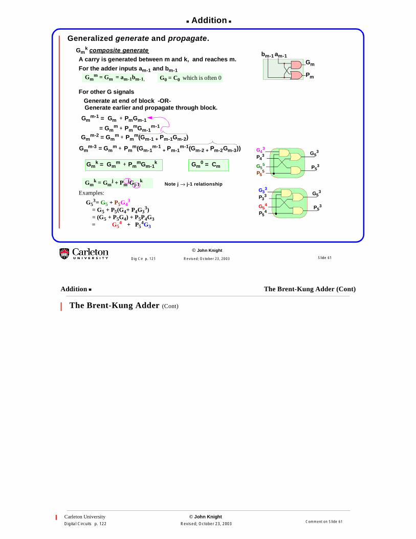
Generalized generate and propagate.
Gmk composite generate
A carry is generated between m and k, and reaches m.
For the adder inputs am-1 and bm-1
For other G signalsGenerate at end of block -OR-Generate earlier and propagate through block.
Note j → j-1 relationship
Examples:
G53= G5 + P5G4
3
= G5 + P5(G4+ P4G33)
= (G5 + P5G4) + P5P4G3= G5
4 + P54G3
am-1bm-1Gm
Pm
G43
P55
G55
P53
P43 G5
3
G33
P54
G54
P53
P33 G5
3
Gmm = Gm = am-1bm-1, G0 = C0 which is often 0
Gmm-1 = Gm + PmGm-1
= Gmm + Pm
mGm-1m-1
Gmm-3 = Gm
m + Pmm(Gm-1
m-1+ Pm-1
m-1(Gm-2 + Pm-2Gm-3))
Gmm-2 = Gm
m + Pmm(Gm-1 + Pm-1Gm-2)
Gmk = Gm
m + PmmGm-1
k Gm0 = Cm
Gmk = Gm
j + PmjGj-1
k
Slide 61
Carleton University © John KnightDigital Circuits p. 122 Revised; October 23, 2003
Addition The Brent-Kung Adder (Cont)
The Brent-Kung Adder (Cont)
Comment on Slide 61
Addition
© John Knight
Dig Cir p. 123 Revised; October 23, 2003
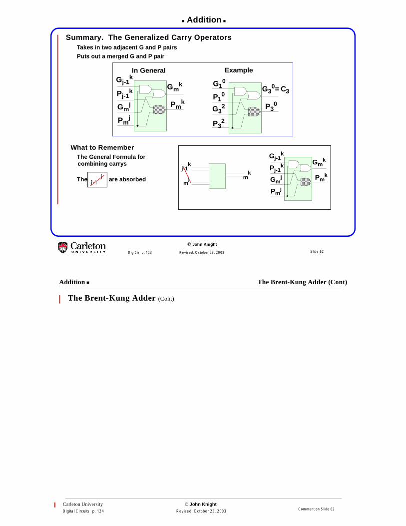
Summary. The Generalized Carry OperatorsTakes in two adjacent G and P pairs
Puts out a merged G and P pair
What to RememberThe General Formula forcombining carrys
The are absorbed
P10
G32
G30= C3
P32
G10
P30
Pj-1k
Gmj
Gmk
Pmj
Gj-1k
Pmk
ExampleIn General
Pj-1k
Gmj
Gmk
Pmj
Gj-1k
Pmk
j-1k
mj m
k
j-1j
Slide 62
Carleton University © John KnightDigital Circuits p. 124 Revised; October 23, 2003
Addition The Brent-Kung Adder (Cont)
The Brent-Kung Adder (Cont)
Comment on Slide 62
Addition
© John Knight
Dig Cir p. 125 Revised; October 23, 2003
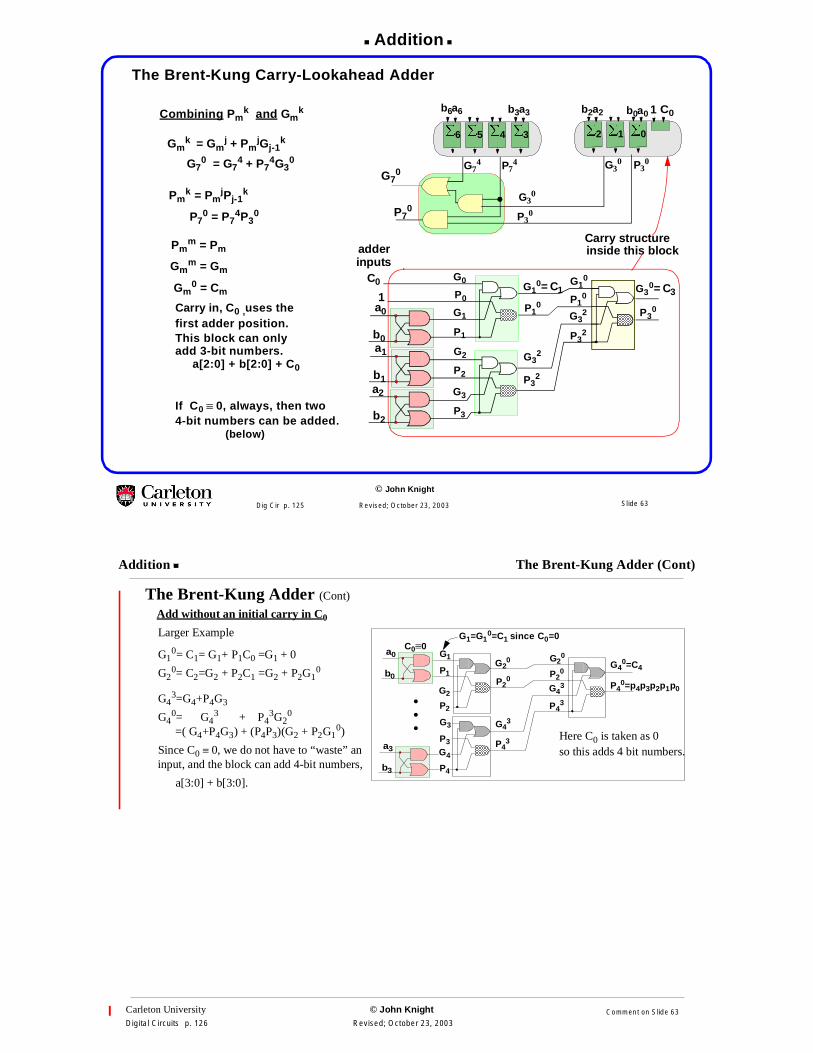
The Brent-Kung Carry-Lookahead Adder
�6
G30
P74
G70
�5 �4 �3
G74
�2
P30
�1 �0
G30
P70
P30
Carry structureinside this block
P0
G1
G10= C1
P1
G0
P10
P2
G3
G32
P3
G2
P32
P10
G32
G30= C3
P32
G10
P30
Combining Pmk and Gm
k
Gmk = Gm
j + PmjGj-1
k
Pmk = Pm
jPj-1k
G70 = G7
4 + P74G3
0
P70 = P7
4P30
b0a0
adderinputs
1
C0
Pmm = Pm
Gmm = Gm
Gm0 = Cm
b0
a0
b1
a1
C01
Carry in, C0 ,uses thefirst adder position.This block can onlyadd 3-bit numbers.
If C0 ≡ 0, always, then two4-bit numbers can be added. b2
a2
b2a2b3a3b6a6
a[2:0] + b[2:0] + C0
(below)
Slide 63
Carleton University © John KnightDigital Circuits p. 126 Revised; October 23, 2003
Addition The Brent-Kung Adder (Cont)
The Brent-Kung Adder (Cont)
Add without an initial carry in C0
Larger Example
G10= C1= G1+ P1C0 =G1 + 0
G20= C2=G2 + P2C1 =G2 + P2G1
0
G43=G4+P4G3
G40= G4
3 + P43G2
0
=( G4+P4G3) + (P4P3)(G2 + P2G10)
Since C0 ≡ 0, we do not have to “waste” aninput, and the block can add 4-bit numbers,
a[3:0] + b[3:0].
P1
G2
G20
P2
G1
P20
P3
G4
G43
P4
G3
P43
P20
G43
G40=C4
P43
G20
P40=p4p3p2p1p0
Here C0 is taken as 0
b0
a0C0≡0
so this adds 4 bit numbers.
G1=G10=C1 since C0=0
b3
a3
•••
Comment on Slide 63
Addition
© John Knight
Dig Cir p. 127 Revised; October 23, 2003
P0
G1
G10= C1
P1
G0
P10
P2
G3
G32
P3
G2
P32
P10
G32
G30= C3
P32
G10
P30
P4
G5
G54
P5
G4
P54
P6
G7
G76
P7
G6
P76
P54
G76
G74
P76
G54
P74
P8
G9
G98
P9
G8
P98
P10
G11
G1110
P11
G10
P1110
G1110
G118
P1110
G98
P118
P98
P30
G74
G70= C7
P74
G30
P70
P70
G118
G110= C11
P118
P110
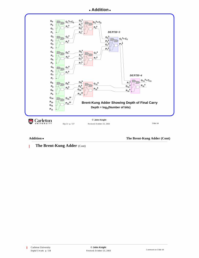
Brent-Kung Adder Showing Depth of Final CarryDepth = log2(Number of bits)
DEPTH=4
DEPTH=3
Slide 64
Carleton University © John KnightDigital Circuits p. 128 Revised; October 23, 2003
Addition The Brent-Kung Adder (Cont)
The Brent-Kung Adder (Cont)
Comment on Slide 64
Addition
© John Knight
Dig Cir p. 129 Revised; October 23, 2003
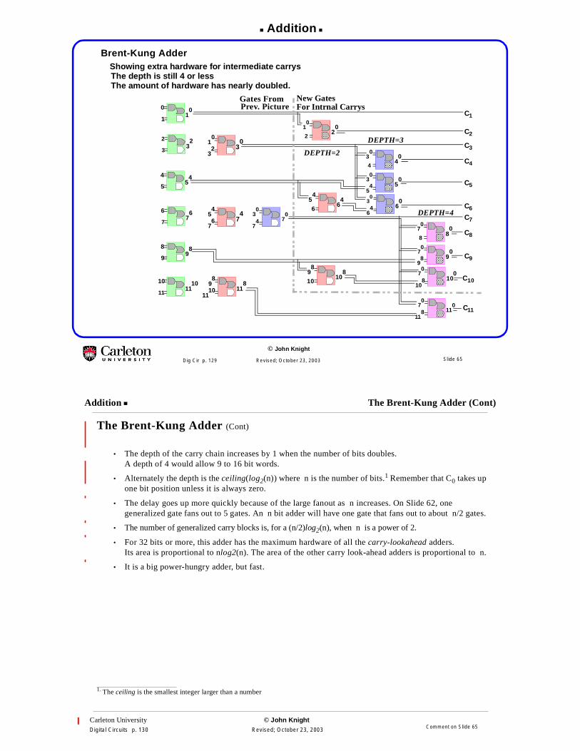
Brent-Kung AdderShowing extra hardware for intermediate carrysThe depth is still 4 or lessThe amount of hardware has nearly doubled.
1100
3322
55
44
7766
9988
1111
1010
301
0
32
745
4
76
1189
8
1110
703
0
74
1107
0
118
201
0
2
403
0
4
503
0
54
664
603
0
64
54
807
0
8
907
0
98
1010
810
070
108
98
C1
C2
C3
C4
C5
C6
C7
C8
C9
C10
C11
Gates FromPrev. Picture
New GatesFor Intrnal Carrys
DEPTH=4
DEPTH=3
DEPTH=2
Slide 65
Carleton University © John KnightDigital Circuits p. 130 Revised; October 23, 2003
Addition The Brent-Kung Adder (Cont)
The Brent-Kung Adder (Cont)
• The depth of the carry chain increases by 1 when the number of bits doubles.A depth of 4 would allow 9 to 16 bit words.
• Alternately the depth is the ceiling(log2(n)) where n is the number of bits.1 Remember that C0 takes upone bit position unless it is always zero.
• The delay goes up more quickly because of the large fanout as n increases. On Slide 62, onegeneralized gate fans out to 5 gates. An n bit adder will have one gate that fans out to about n/2 gates.
• The number of generalized carry blocks is, for a (n/2)log2(n), when n is a power of 2.
• For 32 bits or more, this adder has the maximum hardware of all the carry-lookahead adders.Its area is proportional to nlog2(n). The area of the other carry look-ahead adders is proportional to n.
• It is a big power-hungry adder, but fast.
1. The ceiling is the smallest integer larger than a number
Comment on Slide 65
Addition
© John Knight
Dig Cir p. 131 Revised; October 23, 2003
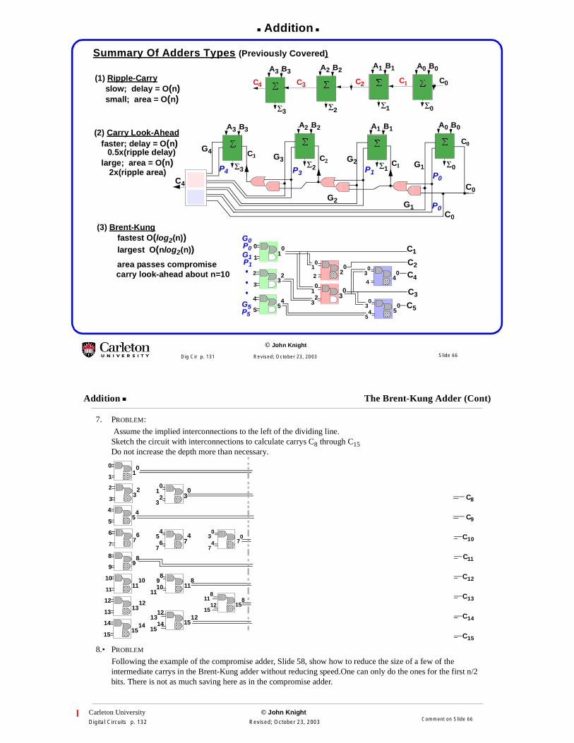
Summary Of Adders Types (Previously Covered)
Σ1
C2
B1A1
� C0C1C4 C3
Σ0
B0A0
�
Σ2
B2A2
�
Σ3
B3A3
�(1) Ripple-Carry
G3
P3
G2P1
G4
P4G1
P0
C3
C0C4
C1
C0
C2
P0G1G2
C0
Σ3
B3A3
�
Σ2
B2A2
�
Σ1
B1A1
�
Σ0
B0A0
�
(2) Carry Look-Ahead
11
00
3322
5544 3
010
32
201
0
2 403
0
4
503
0
54
C1
C2
C4
C3
C5
(3) Brent-Kung
slow; delay = O(n)small; area = O(n)
faster; delay = O(n)
large; area = O(n)
fastest O(log2(n))largest O(nlog2(n))
2x(ripple area)
0.5x(ripple delay)
area passes compromisecarry look-ahead about n=10
P1
G1
P5
G5
P0
G0
Slide 66
Carleton University © John KnightDigital Circuits p. 132 Revised; October 23, 2003
Addition The Brent-Kung Adder (Cont)
7. PROBLEM:
Assume the implied interconnections to the left of the dividing line.Sketch the circuit with interconnections to calculate carrys C8 through C15Do not increase the depth more than necessary.
8.• PROBLEM
Following the example of the compromise adder, Slide 58, show how to reduce the size of a few of theintermediate carrys in the Brent-Kung adder without reducing speed.One can only do the ones for the first n/2bits. There is not as much saving here as in the compromise adder.
1100
33
22
5544
7766
99
88
1111
1010
301
0
32
745
4
76
1189
8
1110
703
0
74
1313
1212
1515
1414 151213
12
1514
15811
8
1512
C10
C11
C12
C8
C9
C13
C14
C15
Comment on Slide 66
Addition
© John Knight
Dig Cir p. 133 Revised; October 23, 2003
Summary Of Adders Types : (About to be covered)
1
0C0A3
B3A2
B2A3
B3A0
B0
Σ
C4 11
11A7
B7A6
B6A5
B5A4
B4C8
1
011
11
Σ STAGE 2 STAGE 16) Carry Select
G3P3
G2P2
G4
P4
G1P1
C1C3
C01
1G1
MUXC4 C0
P4
C2
P3 P2 P1
When P3P2P1P0=1, does not wait for the ripple carry.
5) Carry Skip
C0
Σ3
B3A3
�
Σ2
B2A2
�
Σ1
B1A1
�
Σ0
B0A0
�
Four New Adder Types
Speeds up slowestC0->C4 pathwith littleextra area.
Does not helpother paths.
Doubles area
Very fast pathC0->C4
Stilldelay = O(n)
Select the correct one
Adder for C0=1Adder for C4=1
Adder for C4=0 Adder for C0=0
Calculate answers for bothC0=1 and for C0=0
Slide 67
Carleton University © John KnightDigital Circuits p. 134 Revised; October 23, 2003
Addition Properties of look-ahead adders
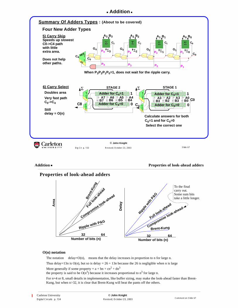
Properties of look-ahead adders
O(n) notationThe notation delay=O(n), means that the delay increases in proportion to n for large n.
Thus delay=13n is O(n), but so is delay = 26 + 13n because the 26 is negligible when n is large
More generally if some property = a + bn + cn2 + dn3
the property is said to be O(n3) because it increases proportional to n3 for large n.
For n=4 or 8, small details in implementation, like buffer sizing, may make the look-ahead faster than Brent-Kung, but when n>32, it is clear that Brent-Kung will beat the pants off the others.
Bre
nt-K
ung
Ripple with P&G
Full lo
ok-a
head
Compromise look-ahead
Brent-Kung
Full look-ahead
Compromise look-ahead
Rippl
ew
ithP&G
Number of bits (n)Number of bits (n)
Del
ayAre
a
32 64 32 64
To the finalcarry out.Some sum bitstake a little longer.
Comment on Slide 67
Addition
© John Knight
Dig Cir p. 135 Revised; October 23, 2003
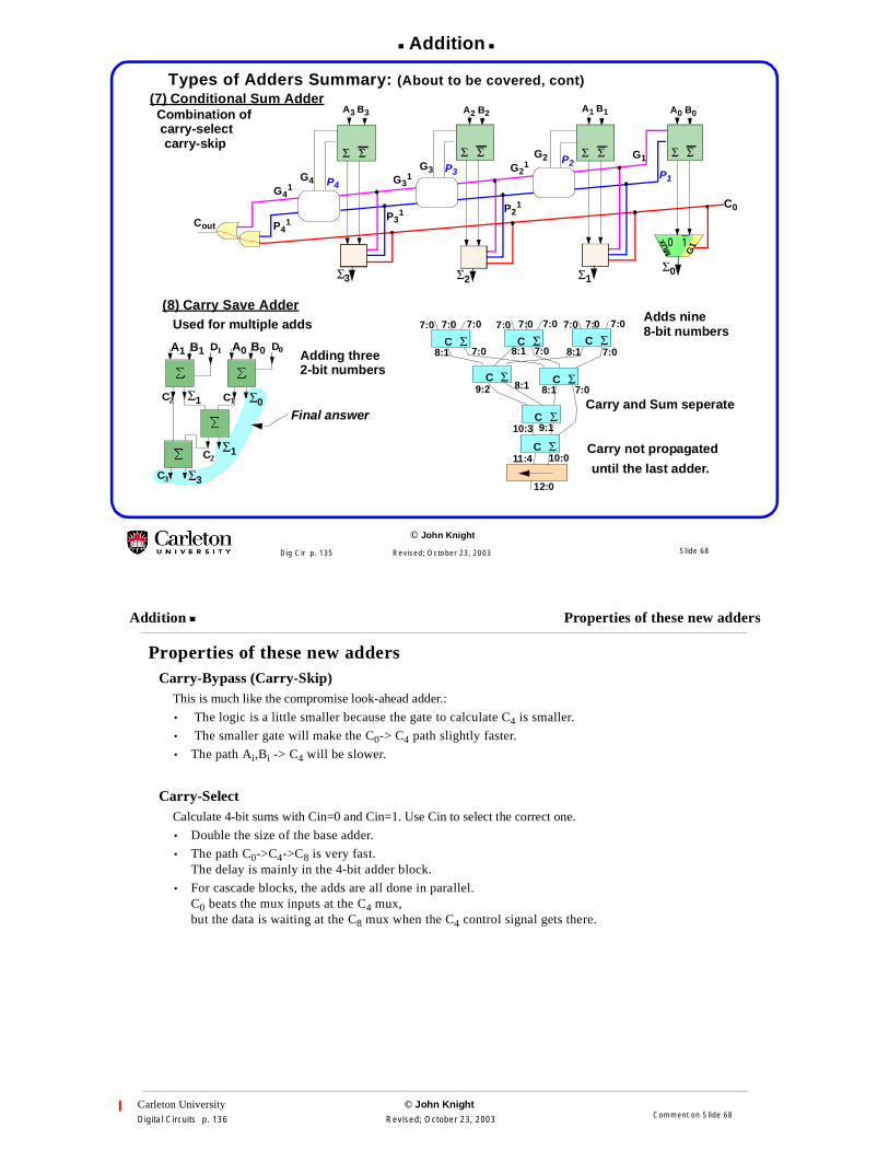
Types of Adders Summary: (About to be covered, cont)(7) Conditional Sum Adder
G3 P3
B2A2B3A3
G2 P2
G4
G1
P1
B0A0B1A1
Cout
G21
P21
G31
P31
P41
G41
0 1
G1
MU
X
Σ
P4
Σ Σ Σ Σ Σ Σ Σ
Σ2Σ0Σ1
C0
Σ3
(8) Carry Save Adder7:0 7:07:0
8:17:08:1 7:0 7:08:1
9:2 8:1 8:1 7:0
10:3 9:1
11:4 10:0
12:0
7:0 7:07:0 7:0 7:07:0
ΣC ΣC ΣC
ΣCΣC
ΣC
ΣC
Combination ofcarry-selectcarry-skip
Used for multiple adds
Carry and Sum seperate
Adds nine8-bit numbers
Carry not propagated
until the last adder.
Σ1
B1A1 D1
C2 Σ0
B0A0
�
D0
C1
�
Σ1C2
�
�
Σ3C3
Adding three2-bit numbers
Final answer
Slide 68
Carleton University © John KnightDigital Circuits p. 136 Revised; October 23, 2003
Addition Properties of these new adders
Properties of these new addersCarry-Bypass (Carry-Skip)
This is much like the compromise look-ahead adder.:
• The logic is a little smaller because the gate to calculate C4 is smaller.
• The smaller gate will make the C0-> C4 path slightly faster.
• The path Ai,Bi -> C4 will be slower.
Carry-SelectCalculate 4-bit sums with Cin=0 and Cin=1. Use Cin to select the correct one.
• Double the size of the base adder.
• The path C0->C4->C8 is very fast.The delay is mainly in the 4-bit adder block.
• For cascade blocks, the adds are all done in parallel.C0 beats the mux inputs at the C4 mux,but the data is waiting at the C8 mux when the C4 control signal gets there.
Comment on Slide 68
Addition
© John Knight
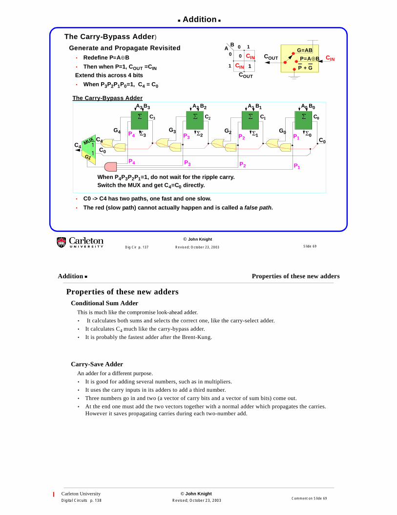
Dig Cir p. 137 Revised; October 23, 2003
The Carry-Bypass Adder)
Generate and Propagate Revisited• Redefine P=A⊕B
• Then when P=1, COUT =CIN
Extend this across 4 bits
• When P3P2P1P0=1, C4 = C0
The Carry-Bypass Adder
• C0 -> C4 has two paths, one fast and one slow.
• The red (slow path) cannot actually happen and is called a false path.
CINCOUT
G=AB
P=A⊕B
P + G
AB
0
1
0 1
0
1
CIN
CIN
COUT
G3P3
Σ3
B3A3
G2P2
G4
P4
G0P1
Σ0
C0
B0A0
�
Σ1
C1
B1A1
�C3�
C0C411G1
MUXC4 C0
P4 Σ2
C2
B2A2
�
P3 P2 P1
When P4P3P2P1=1, do not wait for the ripple carry.Switch the MUX and get C4=C0 directly.
Slide 69
Carleton University © John KnightDigital Circuits p. 138 Revised; October 23, 2003
Addition Properties of these new adders
Properties of these new addersConditional Sum Adder
This is much like the compromise look-ahead adder.
• It calculates both sums and selects the correct one, like the carry-select adder.
• It calculates C4 much like the carry-bypass adder.
• It is probably the fastest adder after the Brent-Kung.
Carry-Save AdderAn adder for a different purpose.
• It is good for adding several numbers, such as in multipliers.
• It uses the carry inputs in its adders to add a third number.
• Three numbers go in and two (a vector of carry bits and a vector of sum bits) come out.
• At the end one must add the two vectors together with a normal adder which propagates the carries.However it saves propagating carries during each two-number add.
Comment on Slide 69
False Paths
© John Knight
Dig Cir p. 139 Revised; October 23, 2003
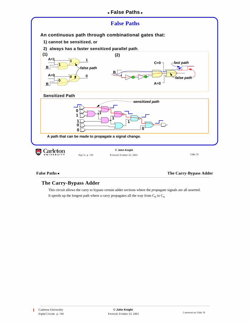
False Paths
An continuous path through combinational gates that:
1) cannot be sensitized, or
2) always has a faster sensitized parallel path.
Sensitized Path
A path that can be made to propagate a signal change.
false path
false path
C=0
A=0
B
A=11
1 1
A=00
0 0
B
Bfast path
(1) (2)
110
1
0
01
1
0
sensitized path
Slide 70
Carleton University © John KnightDigital Circuits p. 140 Revised; October 23, 2003
False Paths The Carry-Bypass Adder
The Carry-Bypass AdderThis circuit allows the carry to bypass certain adder sections where the propagate signals are all asserted.
It speeds up the longest path where a carry propagates all the way from C0 to C4
Comment on Slide 70
False Paths
© John Knight
Dig Cir p. 141 Revised; October 23, 2003
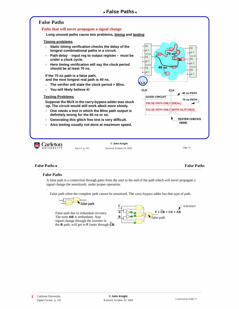
False PathsPaths that will never propagate a signal change
Long unused paths cause two problems, timing and testing
Timing problems• Static timing verification checks the delay of the
longest combinational paths in a circuit.• Path delay - input reg to output register - must be
under a clock cycle.• Here timing verification will say the clock period
should be at least 70 ns.
If the 70 ns path is a false path,and the next longest real path is 40 ns.• The verifier will state the clock period > 80ns.• You will likely believe it!
Testing Problems
Suppose the MUX in the carry-bypass adder was stuckup. The circuit would still work albeit more slowly.• One needs a test in which the 80ns path output is
definitely wrong for the 60 ns or so.• Generating this glitch free test is very difficult.• Also testing usually not done at maximum speed.
1D
C1
1D
C1
1D
C1
1D
C1
1D
C1
1D
C1
40 ns
70 ns
CLK
CLK CLK
GOOD CIRCUIT
FALSE PATH ONLY (IDEAL)
40 ns PATH
TESTER CHECKSHERE
FALSE PATH ONLY (WITH GLITCHES)
70 ns PATH
Slide 71
Carleton University © John KnightDigital Circuits p. 142 Revised; October 23, 2003
False Paths False Paths
False PathsA false path is a connection through gates from the start to the end of the path which will never propagate asignal change (be sensitized) under proper operation..
false path
False path when the complete path cannot be sensitized. The carry-bypass adder has that type of path.
False path due to redundant circuitry. F = CB + CA + AB
false path
false pathThe term AB is redundant. Any
C
A
Bsignal change through the inverter inthe B path, will get to F faster through CB.
redundant
Comment on Slide 71
False Paths
© John Knight
Dig Cir p. 143 Revised; October 23, 2003
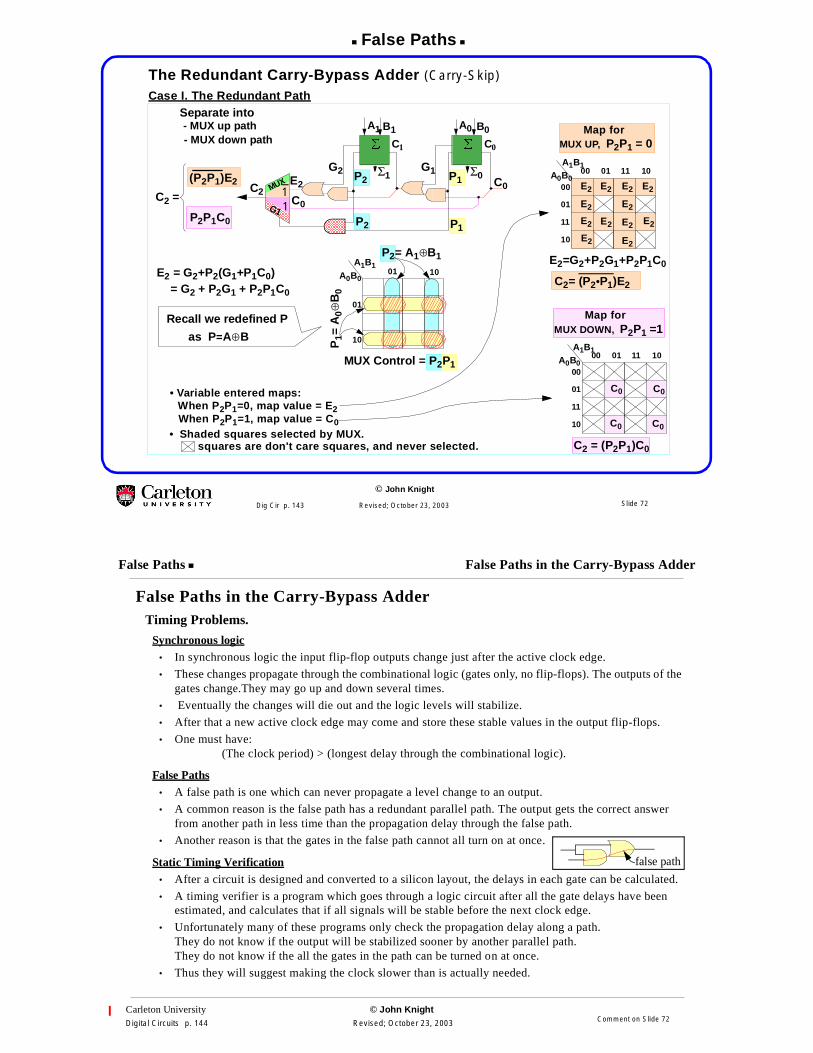
The Redundant Carry-Bypass Adder (Carry-Skip)
Case I. The Redundant Path
G2 P2G1 P1
Σ0
C0
B0A0
�
Σ1
C1
B1A1
�
C0
P2 P1
E211G1
MUXC2C0
01
10
01A0B0
A1B1
00
01
11
10
00 01
C0
C0
C0
C0
11 10A0B0
A1B1
Separate into
C2 =
MUX Control = P2P1
P1=
A0⊕
B0
P2= A1⊕B1
C2 = (P2P1)C0
• Variable entered maps:
MUX DOWN, P2P1 =1
P2P1C0
00
01
11
10
00 01
E2 E2
E2
E2
E2 E2
E2
E2
11 10A0B0
A1B1
E2 E2 E2 E2
E2=G2+P2G1+P2P1C0
MUX UP, P2P1 = 0
C2= (P2•P1)E2
• Shaded squares selected by MUX.squares are don't care squares, and never selected.
When P2P1=1, map value = C0
10
When P2P1=0, map value = E2
(P2P1)E2
Map for
Map for
E2 = G2+P2(G1+P1C0)= G2 + P2G1 + P2P1C0
- MUX up path- MUX down path
as P=A⊕B
Recall we redefined P
Slide 72
Carleton University © John KnightDigital Circuits p. 144 Revised; October 23, 2003
False Paths False Paths in the Carry-Bypass Adder
False Paths in the Carry-Bypass AdderTiming Problems.
Synchronous logic• In synchronous logic the input flip-flop outputs change just after the active clock edge.
• These changes propagate through the combinational logic (gates only, no flip-flops). The outputs of thegates change.They may go up and down several times.
• Eventually the changes will die out and the logic levels will stabilize.
• After that a new active clock edge may come and store these stable values in the output flip-flops.
• One must have:(The clock period) > (longest delay through the combinational logic).
False Paths• A false path is one which can never propagate a level change to an output.
• A common reason is the false path has a redundant parallel path. The output gets the correct answerfrom another path in less time than the propagation delay through the false path.
• Another reason is that the gates in the false path cannot all turn on at once.
Static Timing Verification• After a circuit is designed and converted to a silicon layout, the delays in each gate can be calculated.
• A timing verifier is a program which goes through a logic circuit after all the gate delays have beenestimated, and calculates that if all signals will be stable before the next clock edge.
• Unfortunately many of these programs only check the propagation delay along a path.They do not know if the output will be stabilized sooner by another parallel path.They do not know if the all the gates in the path can be turned on at once.
• Thus they will suggest making the clock slower than is actually needed.
false path
Comment on Slide 72
False Paths
© John Knight
Dig Cir p. 145 Revised; October 23, 2003
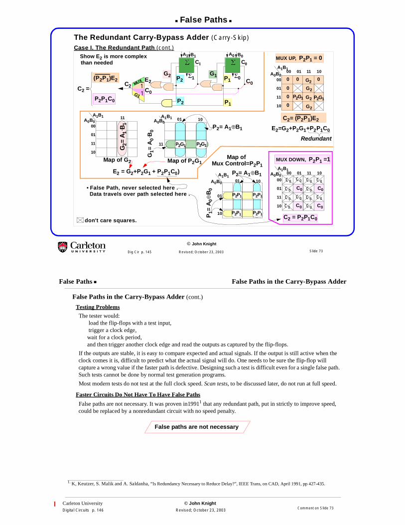
The Redundant Carry-Bypass Adder (Carry-Skip)
Case I. The Redundant Path (cont.)
G2 P2G1 P1
Σ0
C0
B0A0
�
Σ1
C1
B1A1
�
C0
P2 P1
E211G1
MUXC2C0
01
10
01A0B0
A1B1
11
A0B0
A1B1
00
01
11
10
11A0B0
A1B1
E2 = G2+P2G1 + P2P1C0)
C2 =
P1=
A0⊕
B0
P2= A1⊕B1
P2= A1⊕B1
C2 = P2P1C0
G1=
A0·
B0
G2=
A1·
B1
MUX DOWN, P2P1 =1
P2P1C0
00
01
11
10
00 01
0 0
0
0
0
G2
11 10A0B0
A1B1
0
E2=G2+P2G1+P2P1C0
MUX UP, P2P1 = 0
C2= (P2P1)E2
don't care squares.
10
01 10
G2
G2
G2
P2G1P2G1
• False Path, never selected here .Data travels over path selected here .
00
01
11
10
00 01
C0
C0
C0
C0
11 10A0B0
A1B1
C0
C0
C0
C0C0C0
C0
C0
C0
C0 C0
C0
P2G1 P2G1
P2P1 P2P1
P2P1P2P1
(P2P1)E2
Map ofMux Control=P2P1
Show E2 is more complexthan needed
Redundant
Map of P2G1Map of G2
Slide 73
Carleton University © John KnightDigital Circuits p. 146 Revised; October 23, 2003
False Paths False Paths in the Carry-Bypass Adder
False Paths in the Carry-Bypass Adder (cont.)
Testing Problems
The tester would:load the flip-flops with a test input,trigger a clock edge,wait for a clock period,and then trigger another clock edge and read the outputs as captured by the flip-flops.
If the outputs are stable, it is easy to compare expected and actual signals. If the output is still active when theclock comes it is, difficult to predict what the actual signal will do. One needs to be sure the flip-flop willcapture a wrong value if the faster path is defective. Designing such a test is difficult even for a single false path.Such tests cannot be done by normal test generation programs.
Most modern tests do not test at the full clock speed. Scan tests, to be discussed later, do not run at full speed.
Faster Circuits Do Not Have To Have False Paths
False paths are not necessary. It was proven in19911 that any redundant path, put in strictly to improve speed,could be replaced by a nonredundant circuit with no speed penalty.
1. K, Keutzer, S. Malik and A. Saldanha, “Is Redundancy Necessary to Reduce Delay?”, IEEE Trans, on CAD, April 1991, pp 427-435.
False paths are not necessary
Comment on Slide 73
False Paths
© John Knight
Dig Cir p. 147 Revised; October 23, 2003
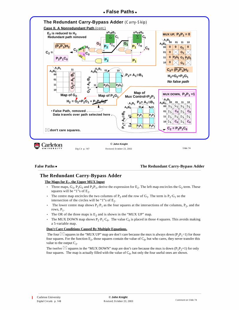
The Redundant Carry-Bypass Adder (Carry-Skip)
Case II. A Nonredundant Path (cont.)
G2 P2G1 P1
Σ0
C0
B0A0
�
Σ1
C1
B1A1
�
C0
P2 P1
H211G1
MUXC2C0
01
10
01A0B0
A1B1
11
A0B0
A1B1
00
01
11
10
11A0B0
A1B1
H2 = G2+P2G1 + P2P1C0)
C2 =
P1=
A0⊕
B0
P2= A1⊕B1
Map of P2G1
P2= A1⊕B1
Map of G2
C2 = P2P1C0
G1=
A0·
B0
G2=
A1·
B1
MUX DOWN, P2P1 =1
P2P1C0
00
01
11
10
00 01
0 0
0
0
0
G2
11 10A0B0
A1B1
0
H2=G2+P2G1
MUX UP, P2P1 = 0
C2= (P2P1)H2
don't care squares.
10
01 10
G2
G2
G2
P2G1P2G1
• False Path, removed .Data travels over path selected here .
00
01
11
10
00 01
C0
C0
C0
C0
11 10A0B0
A1B1
C0
C0
C0
C0C0C0
C0
C0
C0
C0 C0
C0
P2G1 P2G1
P2P1 P2P1
P2P1P2P1
(P2P1)H2
Map ofMux Control=P2P1
E2 is reduced to H2Redundant path removed
No false path
Slide 74
Carleton University © John KnightDigital Circuits p. 148 Revised; October 23, 2003
False Paths The Redundant Carry-Bypass Adder
The Redundant Carry-Bypass AdderThe Maps for E2, the Upper MUX Input
• Three maps, G2, P2G2 and P2P1, derive the expression for E2. The left map encircles the G2 term. Thesesquares will be “1”s of E2.
• The centre map encircles the two columns of P2 and the row of G1. The term is P2·G1 so theintersection of the circles will be “1”s of E2.
• The lower centre map shows P2·P1 as the four squares at the intersections of the columns, P2, and therows, P1.
• The OR of the three maps is E2 and is shown in the “MUX UP” map.
• The MUX DOWN map shows P2·P1·C0. The value C0 is placed in those 4 squares. This avoids makinga 5-variable map.
Don't Care Conditions Caused By Multiple Equations.
The four squares in the “MUX UP” map are don’t care because the mux is always down (P2P1=1) for thosefour squares. For the function E2, those squares contain the value of C0, but who cares, they never transfer thisvalue to the output C2.
The twelve squares in the “MUX DOWN” map are don’t care because the mux is down (P1P2=1) for onlyfour squares. The map is actually filled with the value of C0, but only the four useful ones are shown.
Comment on Slide 74
False Paths
© John Knight
Dig Cir p. 149 Revised; October 23, 2003
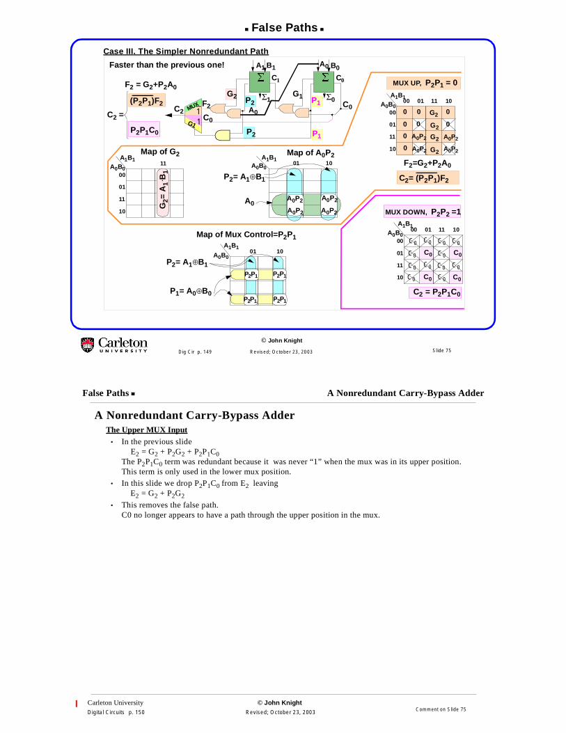
Case III. The Simpler Nonredundant Path
G2 P2G1 P1
Σ0
C0
B0A0
�
Σ1
C1
B1A1
�
C0
P2 P1
01 10A0B0
A1B1
01 10A0B0
A1B1
00
01
11
10
11A0B0
A1B1
00
01
11
10
00 01
C0
C0
C0
C0
11 10A0B0
A1B1
F2 = G2+P2A0
C2 =
Map of Mux Control=P2P1
P1= A0⊕B0
P2= A1⊕B1
Map of A0P2Map of G2
C2 = P2P1C0
A0G2=
A1·
B1
MUX DOWN, P2P2 =1
(P2P1)F2
P2P1C0
00
01
11
10
00 01
0 0
0 0
0
0
0
G2
11 10A0B0
A1B1
0
F2=G2+P2A0
MUX UP, P2P1 = 0
C2= (P2P1)F2
A0
P2= A1⊕B1
F211G1
MUXC2C0
G2
G2
G2
A0P2 A0P2
A0P2 A0P2
A0P2 A0P2
A0P2 A0P2
C0
C0
C0
C0C0C0
C0
C0
C0
C0 C0
C0
P2P1 P2P1
P2P1P2P1
Faster than the previous one!
Slide 75
Carleton University © John KnightDigital Circuits p. 150 Revised; October 23, 2003
False Paths A Nonredundant Carry-Bypass Adder
A Nonredundant Carry-Bypass AdderThe Upper MUX Input
• In the previous slideE2 = G2 + P2G2 + P2P1C0
The P2P1C0 term was redundant because it was never “1” when the mux was in its upper position.This term is only used in the lower mux position.
• In this slide we drop P2P1C0 from E2 leavingE2 = G2 + P2G2
• This removes the false path.C0 no longer appears to have a path through the upper position in the mux.
Comment on Slide 75
Adders
© John Knight
Dig Cir p. 151 Revised; October 23, 2003
Adders
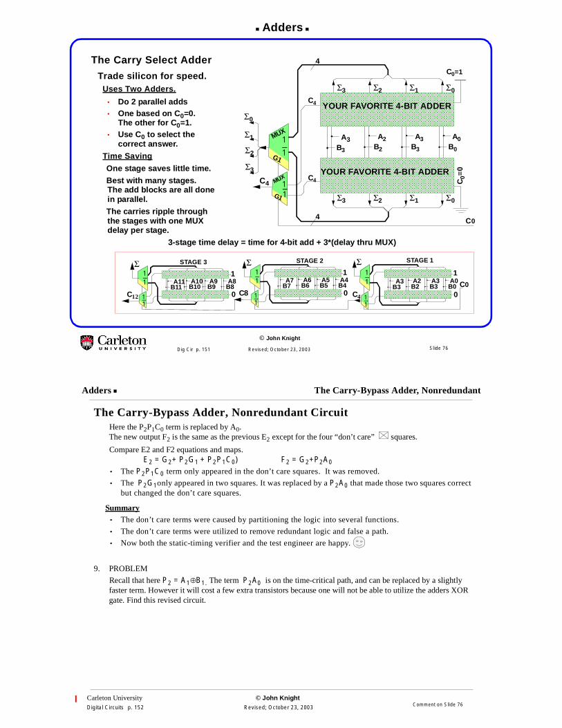
The Carry Select Adder
Trade silicon for speed.Uses Two Adders.
• Do 2 parallel adds• One based on C0=0.
The other for C0=1.• Use C0 to select the
correct answer.Time Saving
One stage saves little time.Best with many stages.The add blocks are all donein parallel.The carries ripple throughthe stages with one MUXdelay per stage.
3-stage time delay = time for 4-bit add + 3*(delay thru MUX)
A3B3
A2B2
A3B3
A0B0
Σ3 Σ2 Σ1 Σ0
C0=1
1
1G1
MUX
Σ3 Σ2 Σ1 Σ0
C0=
0
11G1
MUXC4
Σ3
Σ2
Σ1
Σ0
YOUR FAVORITE 4-BIT ADDER
YOUR FAVORITE 4-BIT ADDER
C4
C4
4
4 C0
1
0C0A3
B3A2B2
A3B3
A0B0
Σ
C4 11
11A7
B7A6
B6A5B5
A4B4
C8
1
011
11
Σ
A11B11
A10B10
A9B9
A8B8
C12
1
011
11
Σ STAGE 3 STAGE 2 STAGE 1
Slide 76
Carleton University © John KnightDigital Circuits p. 152 Revised; October 23, 2003
Adders The Carry-Bypass Adder, Nonredundant
The Carry-Bypass Adder, Nonredundant CircuitHere the P2P1C0 term is replaced by A0.The new output F2 is the same as the previous E2 except for the four “don’t care” squares.
Compare E2 and F2 equations and maps.E2 = G2+ P2G1 + P2P1C0) F2 = G2+P2A0
• The P2P1C0 term only appeared in the don’t care squares. It was removed.
• The P2G1only appeared in two squares. It was replaced by a P2A0 that made those two squares correctbut changed the don’t care squares.
Summary• The don’t care terms were caused by partitioning the logic into several functions.
• The don’t care terms were utilized to remove redundant logic and false a path.
• Now both the static-timing verifier and the test engineer are happy.
9. PROBLEM
Recall that here P2 = A1⊕B1. The term P2A0 is on the time-critical path, and can be replaced by a slightlyfaster term. However it will cost a few extra transistors because one will not be able to utilize the adders XORgate. Find this revised circuit.
Comment on Slide 76
Adders
© John Knight
Dig Cir p. 153 Revised; October 23, 2003
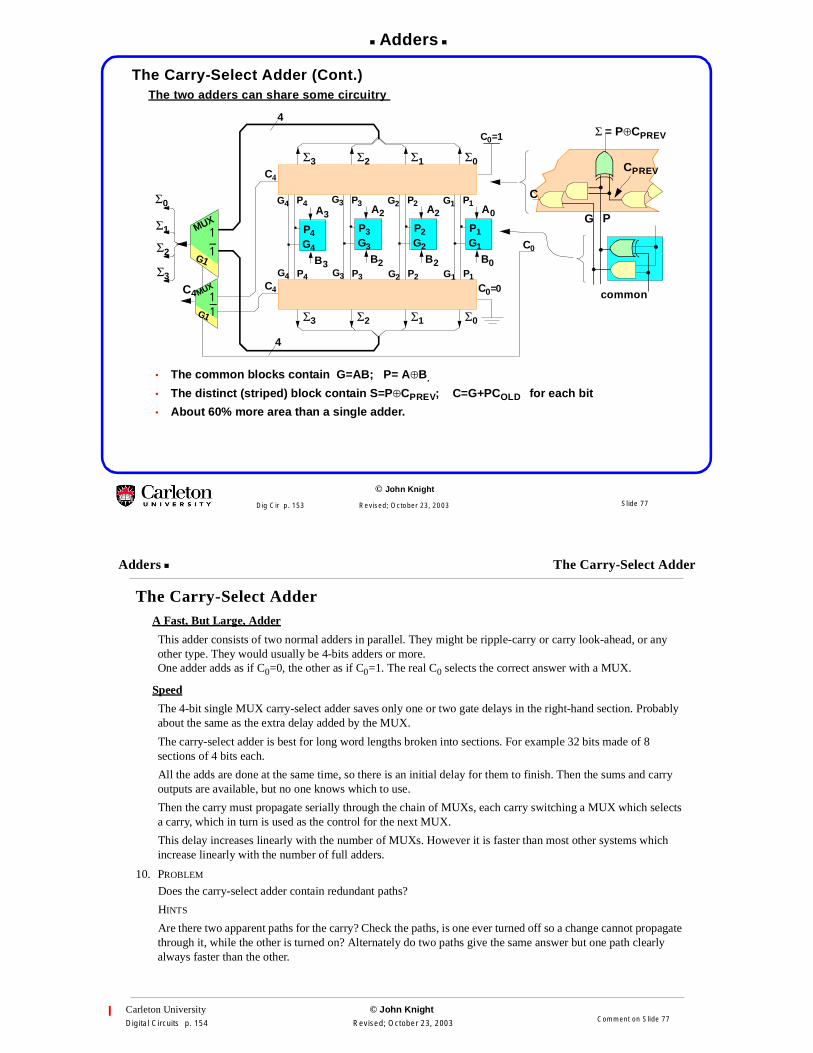
The Carry-Select Adder (Cont.)The two adders can share some circuitry
• The common blocks contain G=AB; P= A⊕B.
• The distinct (striped) block contain S=P⊕CPREV; C=G+PCOLD for each bit
• About 60% more area than a single adder.
C0
B3
A3
P4G4
B2
A2
P3G3
B2
A2
P2G2
B0
A0
P1G1
Σ3 Σ2 Σ1 Σ0C4
C0=1
1
1G1
MUX
Σ3 Σ2 Σ1 Σ0
C4
P4G4 P3G3 P2G2 P1G1
C0=011G1
MUXC4
Σ3
Σ2
Σ1
Σ0
4
4
P4G4 P3G3 P2G2 P1G1
Σ = P⊕CPREV
C
G
CPREV
P
common
Slide 77
Carleton University © John KnightDigital Circuits p. 154 Revised; October 23, 2003
Adders The Carry-Select Adder
The Carry-Select AdderA Fast, But Large, Adder
This adder consists of two normal adders in parallel. They might be ripple-carry or carry look-ahead, or anyother type. They would usually be 4-bits adders or more.One adder adds as if C0=0, the other as if C0=1. The real C0 selects the correct answer with a MUX.
Speed
The 4-bit single MUX carry-select adder saves only one or two gate delays in the right-hand section. Probablyabout the same as the extra delay added by the MUX.
The carry-select adder is best for long word lengths broken into sections. For example 32 bits made of 8sections of 4 bits each.
All the adds are done at the same time, so there is an initial delay for them to finish. Then the sums and carryoutputs are available, but no one knows which to use.
Then the carry must propagate serially through the chain of MUXs, each carry switching a MUX which selectsa carry, which in turn is used as the control for the next MUX.
This delay increases linearly with the number of MUXs. However it is faster than most other systems whichincrease linearly with the number of full adders.
10. PROBLEM
Does the carry-select adder contain redundant paths?
HINTS
Are there two apparent paths for the carry? Check the paths, is one ever turned off so a change cannot propagatethrough it, while the other is turned on? Alternately do two paths give the same answer but one path clearlyalways faster than the other.
Comment on Slide 77
Conditional Sum Adder
© John Knight
Dig Cir p. 155 Revised; October 23, 2003
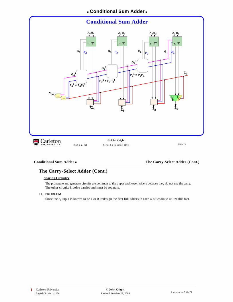
Conditional Sum Adder
G3 P3
B3A3B4A4
G2 P2G4 G1 P1
B1A1B2A2
Cout
G21
P21 = P2P1
G31
P31 = P3P2
1
P41 = P4P3
1
G41
0 1
G1
MU
X
Σ
P4
Σ Σ Σ Σ Σ Σ Σ
Σ4 Σ3Σ1Σ2
C0
Slide 78
Carleton University © John KnightDigital Circuits p. 156 Revised; October 23, 2003
Conditional Sum Adder The Carry-Select Adder (Cont.)
The Carry-Select Adder (Cont.)Sharing Circuitry
The propagate and generate circuits are common to the upper and lower adders because they do not use the carry.The other circuits involve carries and must be separate.
11. PROBLEM
Since the c0 input is known to be 1 or 0, redesign the first full-adders in each 4-bit chain to utilize this fact.
Comment on Slide 78
Conditional Sum Adder
© John Knight
Dig Cir p. 157 Revised; October 23, 2003
G4 P4
B3A3
Calculate in the adder box
Cout = Gn0
C0
G31 = G3 + P3G2
1
P31 = P3P2
1G41 = G4 + P4G3
1
P41 = P4P3
1
Σ Σ
Σ3
Gk+11 = carry out from the kth adder
Gk+12 = carry out from the kth adder
Pn1 = PnPn-1 · · · P2P1
Sum Σk=Pk if Ck-1=1
Pn1 = PnPn-1
1
Gn1 = Gn + PnGn-1
1
Gk if Ck-1=0Σ if Ck=0
Σk-1 = Ak-1⊕Bk-1
Σ if Ck=1Carry out Ck = Σk-1 = Ak-1⊕Bk-1⊕1
Gk = Ak-1Bk-1
Pk = Ak-1+Bk-1
Select the correct sum to send outSelect the right carry to send on.
ignoring C0. (C0=0)
Gk+10 = carry out from the kth adder
ignoring G1,P1, and C0. (G1=0=C0)
a bit can propagate C0� Cout
= PnPn-1 · · · P2P1
If (Pn1 ==1), then
Calculate both sum and carry values
Slide 79
Carleton University © John KnightDigital Circuits p. 158 Revised; October 23, 2003
Conditional Sum Adder The Conditional-Sum Adder
The Conditional-Sum AdderAt one time considered to be the fastest adder theoretically.It combines features of the carry look-ahead, the carry-select, and the carry-bypass adders.
Each adder block calculates:
P = carry out if there is a carry in, Cout(C0=1).G= carry out if it is independent of a carry in, Cout(C0=0).Σ = sum out if carry in is 0, Σ(Cin=0).Σ = sum out if carry in is 1, Σ(Cin=1).
Select the right carry and the right sum outside the adder block
Outside the adder block the previous P and G lines along with C0 are used to select the proper sum.The proper carry out is G if C0=1 and P if C0=0However the proper one is not selected immediately. Both are passed on to the next adder block.The next block upgrades P and G and passes them on.
The carry out from a block of (usually four) adders is selected from the previous P and G by C0.
Comment on Slide 79
Conditional Sum Adder
© John Knight
Dig Cir p. 159 Revised; October 23, 2003
Conditional Sum Adder
G3
P3
B2A2B3A3
G2
P2
G4
G1
P1
B0A0B1A1
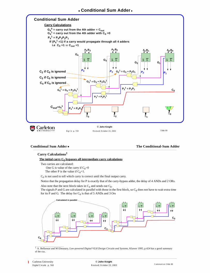
Carry Calculations
Cout=G40
C0
G21 = G2 + P2G1
P21 = P2P1
G31 = G3 + P3G2
1
P31 = P3P2
1
P41 = P4P3
1
G41 = G4 + P4G3
1
1 1
Σ
P4
Σ Σ Σ Σ Σ Σ Σ
Σ3 Σ2 Σ1
G40 = carry out from the 4th adder = Cout
G41 = carry out from the 4th adder with C0 =0
Σ0
P41 = P4P3P2P1
i.e C0 =1 � Cout =1
C3 if C0 is ignored
C4 if C0 is ignored
C2 if C0 is ignored
If (P41 =1) if a carry would propagate through all 4 adders
Slide 80
Carleton University © John KnightDigital Circuits p. 160 Revised; October 23, 2003
Conditional Sum Adder The Conditional-Sum Adder
Carry Calculations1
The initial carry C0 bypasses all intermediate carry calculations
Two carries are calculated:One G is value of the carry if C0=0The other P is the value if C0=1.
C0 is not used to tell which carry is correct until the final output carry.
Notice that the propagation delay for P is exactly that of the carry-bypass adder, the delay of 4 ANDs and 2 ORs.
Also note that the next block takes in C4 and sends out C8.The signals P and G are calculated in parallel with those in the first block, so C8 does not have to wait extra timefor its P and G. The delay for C8 is that of 5 ANDs and 3 Ors
1. A. Bellaouar and M Elmasary, Low-powered Digital VLSI Design Circuits and Systems, Kluwer 1995, p.424 has a good summaryof the csa..
Σ Σ Σ Σ Σ Σ Σ Σ
Σ Σ Σ Σ Σ Σ Σ Σ
C8
C4
C0
Calculated in parallel
Comment on Slide 80
Conditional Sum Adder
© John Knight
Dig Cir p. 161 Revised; October 23, 2003
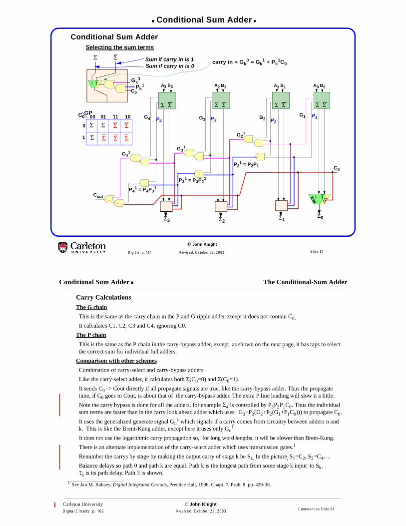
Conditional Sum Adder
G3 P3
B2A2B3A3
G2 P2G4
G1 P1
B0A0B1A1
Selecting the sum terms
Cout
C0
G21
P21 = P2P1
G31
P31 = P3P2
1
P41 = P4P3
1
G41
1 1
G1
MU
X
Σ
P4
Σ Σ Σ Σ Σ Σ Σ
Σ3 Σ2Σ1
Pk1
C0
Gk1
Σ Σ
1 1
GP00 01 11 10
0
1
Σ
Σ
Σ
Σ
Σ
Σ
Σ
Σ
C0
Sum if carry in is 1Sum if carry in is 0
Σ0
carry in = Gk0 = Gk
1 + Pk1C0
Slide 81
Carleton University © John KnightDigital Circuits p. 162 Revised; October 23, 2003
Conditional Sum Adder The Conditional-Sum Adder
Carry CalculationsThe G chain
This is the same as the carry chain in the P and G ripple adder except it does not contain C0.
It calculates C1, C2, C3 and C4, ignoring C0.
The P chain
This is the same as the P chain in the carry-bypass adder, except, as shown on the next page, it has taps to selectthe correct sum for individual full adders.
Comparison with other schemes
Combination of carry-select and carry-bypass adders
Like the carry-select adder, it calculates both Σ(C0=0) and Σ(C0=1).
It sends C0 -> Cout directly if all propagate signals are true, like the carry-bypass adder. Thus the propagatetime, if C0 goes to Cout, is about that of the carry-bypass adder. The extra P line loading will slow it a little.
Note the carry bypass is done for all the adders, for example Σ4 is controlled by P3P2P1C0. Thus the individualsum terms are faster than in the carry look ahead adder which uses G3+P3(G2+P2(G1+P1C0))) to propagate C0.
It uses the generalized generate signal Gnk which signals if a carry comes from circuitry between adders n and
k. This is like the Brent-Kung adder, except here it uses only Gn1
It does not use the logarithmic carry propagation so, for long word lengths, it will be slower than Brent-Kung.
There is an alternate implementation of the carry-select adder which uses transmission gates.1
Renumber the carrys by stage by making the output carry of stage k be Sk. In the picture, S1=C2, S2=C4, ...
Balance delays so path 0 and path k are equal. Path k is the longest path from some stage k input to Sk.τk is its path delay. Path 3 is shown.
1. See Jan M. Rabaey, Digital Integrated Circuits, Prentice Hall, 1996, Chapt. 7, Prob. 8, pp. 429-30.
Comment on Slide 81
Reducing Delay By Gradually Increasing Stage Length
© John Knight
Dig Cir p. 163 Revised; October 23, 2003
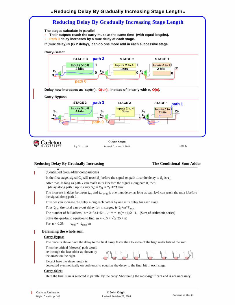
Reducing Delay By Gradually Increasing Stage Length
The stages calculate in parallel• Their outputs reach the carry muxs at the same time (with equal lengths).• Path 0 delay increases by a mux delay at each stage.
If (mux delay) ≈ (G P delay), can do one more add in each successive stage.
Carry-Select
Delay now increases as sqrt(n), O(√n), instead of linearly with n, O(n).
Carry-Bypass
C0C2 1
1
C5 11
C9 11
STAGE 3 STAGE 1
Inputs 2 to 4Inputs 5 to 8
STAGE 2
4 bits 3bits
path 3
Inputs 0 to 12 bits
path 0
1
0
1
0
1
0
C0C2 1
1
C5 11
C9 11
STAGE 3 STAGE 1
Inputs 5 to 8
STAGE 2
4 bits
path 3
path 0
Inputs 2 to 43bits 2 bits
Inputs 0 to 1S3 S2 S1
path 1
Slide 82
Carleton University © John KnightDigital Circuits p. 164 Revised; October 23, 2003
Reducing Delay By Gradually Increasing The Conditional-Sum Adder
(Continued from adder comparisons)
In the first stage, signal C0 will reach S1 before the signal on path 1, so the delay to S1 is τ1.
After that, as long as path k can reach mux k before the signal along path 0, then(delay along path 0 up to carry Sk) = τ0k = τ1+k*τmux
The increase in delay between τ0k and τ0(k+1) is one mux delay, as long as path k+1 can reach the mux k beforethe signal along path 0.
Thus we can increase the delay along each path k by one mux delay for each stage.
Thus τ0m, the total carry-out delay for m stages, is τ1+m*τmux
The number of full adders, n = 2+3+4+5+. . .+ m = m(m+1)/2 - 1. (Sum of arithmetic series)
Solve the quadratic equation to find m = -0.5 + √(2.25 + n)
For n>>2.25 τ0m ≈ τmux√n
Balancing the whole sumCarry-Bypass
The circuits above have the delay to the final carry faster than to some of the high order bits of the sum.
Then the critical (slowest) path wouldbe through the last adder as shown bythe arrow on the right.
Except here the stage length isdecreased symmetrically on both ends to equalize the delay to the final bit in each stage.
Carry-Select
Here the final sum is selected in parallel by the carry. Shortening the most-significant end is not necessary.
Comment on Slide 82
Reducing Delay By Gradually Increasing Stage Length
© John Knight
Dig Cir p. 165 Revised; October 23, 2003
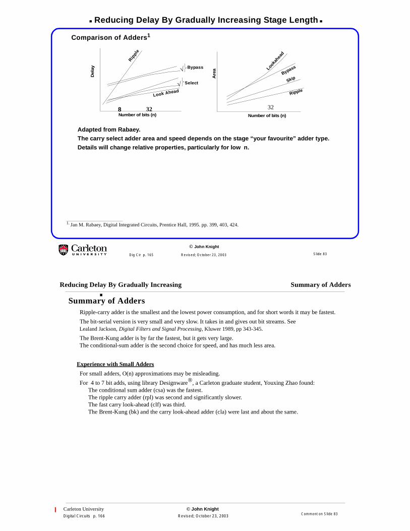
Comparison of Adders1
Adapted from Rabaey.The carry select adder area and speed depends on the stage “your favourite” adder type.
Details will change relative properties, particularly for low n.
1. Jan M. Rabaey, Digital Integrated Circuits, Prentice Hall, 1995. pp. 399, 403, 424.
Ripple
SkipBypassLoo
kahea
d
Number of bits (n)
Are
a
Look Ahead
Select
Rippl
e
Del
ay
Number of bits (n)32
√
Bypass√
328
Slide 83
Carleton University © John KnightDigital Circuits p. 166 Revised; October 23, 2003
Reducing Delay By Gradually Increasing Summary of Adders
Summary of AddersRipple-carry adder is the smallest and the lowest power consumption, and for short words it may be fastest.
The bit-serial version is very small and very slow. It takes in and gives out bit streams. SeeLealand Jackson, Digital Filters and Signal Processing, Kluwer 1989, pp 343-345.
The Brent-Kung adder is by far the fastest, but it gets very large.The conditional-sum adder is the second choice for speed, and has much less area.
Experience with Small Adders
For small adders, O(n) approximations may be misleading.
For 4 to 7 bit adds, using library Designware, a Carleton graduate student, Youxing Zhao found:The conditional sum adder (csa) was the fastest.The ripple carry adder (rpl) was second and significantly slower.The fast carry look-ahead (clf) was third.The Brent-Kung (bk) and the carry look-ahead adder (cla) were last and about the same.
Comment on Slide 83
Reducing Delay By Gradually Increasing Stage Length
© John Knight
Dig Cir p. 167 Revised; October 23, 2003
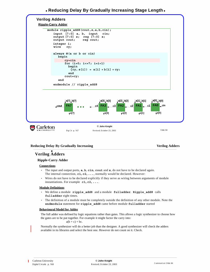
Verilog AddersRipple-Carry Adder
module ripple_add8(cout,s,a,b,cin);input [7:0] a, b, input cin;output [7:0] s; reg [7:0] s;output cout; reg cout;integer i;wire cy;
always @(a or b or cin)begin
cy=cinfor (i=0; i<=7; i=i+1)
begin{cy, s[i]) = a[i] + b[i] + cy;
endcout=cy;
end
endmodule // ripple_add8
s[0]
cinc1
b[0]a[0]
FA0
s[2]
c3
a[2]
FA2
b[2]
s[1]
c2
a[1]
FA1
b[1]
s[3]
c4
a[3]
FA3
b[3]
s[7]
cout
a[7]
FA7
b[7]
Slide 84
Carleton University © John KnightDigital Circuits p. 168 Revised; October 23, 2003
Reducing Delay By Gradually Increasing Verilog Adders
Verilog AddersRipple-Carry Adder
Connections• The input and output ports, a, b, cin, cout and s, do not have to be declared again.
The internal connection, c1, c2, ..., normally would be declared. However:
• Wires do not have to be declared explicitly if they serve as wiring between arguments of moduleinstantiations. For example c1, c2, ....
Module Definitions• We define a module ripple_add8 and a module fulladder. Ripple_add8 calls
fulladder eight times.
• The definition of a module must be completely outside the definition of any other module. Note theendmodule statement for ripple_add8 came before module fulladder started
Behavioural Model for Adder
The full adder was defined by logic equations rather than gates. This allows a logic synthesizer to choose howthe gates are to be put together. For example it might factor the carry into:
a(b + c) + bc.
Normally the synthesizer will do a better job than the designer. A good synthesizer will check the addersavailable in its libraries and select the best one. However do not count on it. Check.
Comment on Slide 84
Reducing Delay By Gradually Increasing Stage Length
© John Knight
Dig Cir p. 169 Revised; October 23, 2003
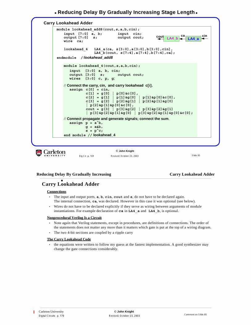
Carry Lookahead Addermodule lookahead_add8(cout,s,a,b,cin);
input [7:0] a, b; input cin;output [7:0] s; output cout;wire ca;
lookahead_4 LA4_a(ca, s[3:0],a[3:0],b[3:0],cin],LA4_b(cout, s[7:4],a[7:4],b[7:4],ca];
endmodule //lookahead_add8
module lookahead_4(cout,s,a,b,cin);
input [3:0] a, b, cin;output [3:0] s; output cout;wires [3:0] c, p, g;
// Connect the carry, cin, and carry lookahead c[i].assign c[0] = cin,
c[1] = g[0] | p[0]&c[0],c[2] = g[1] | p[1]&g[0] | p[1]&p[0]&c[0],c[3] = g[2] | p[2]&g[1] | p[2]&p[1]&g[0]| p[2]&p[1]&p[0]&c[0],cout = g[3] | p[3]&g[2] | p[3]&p[2]&g[1]| p[3]&p[2]&p[1]&g[0] | p[3]&p[2]&p[1]&p[0]&c[0];
// Connect propagate and generate signals; connect the sum.assign p = a^b,
g = a&b,s = p^c;
end module // lookahead_4
cout ca cinLA4_b LA4_a
Slide 85
Carleton University © John KnightDigital Circuits p. 170 Revised; October 23, 2003
Reducing Delay By Gradually Increasing Carry Lookahead Adder
Carry Lookahead AdderConnections
• The input and output ports, a, b, cin, cout and s, do not have to be declared again.The internal connection, ca, was declared. However in this case it was optional (see below).
• Wires do not have to be declared explicitly if they serve as wiring between arguments of moduleinstantiations. For example declaration of ca in LA4_a and LA4_b, is optional.
Nonprocedural Verilog Is a Circuit• Note again that Verilog statements, except in procedures, are definitions of connections. The order of
the statements does not matter any more than it matters which gate is put at the top of a wiring diagram.
• The two 4-bit sections are coupled by a ripple carry
The Carry Lookahead Code• the equations were written to follow my guess at the fastest implementation. A good synthesizer may
change the gate connections considerably.
Comment on Slide 85
Reducing Delay By Gradually Increasing Stage Length
© John Knight
Dig Cir p. 171 Revised; October 23, 2003
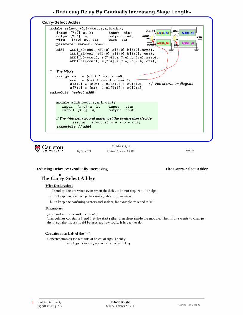
Carry-Select Addermodule select_add8(cout,s,a,b,cin);
input [7:0] a, b; input cin;output [7:0] s; output cout;wire [7:0] s0, s1; wire ca;parameter zero=0, one=1;
add4 ADD4_a0(ca0, s[3:0],a[3:0],b[3:0],zero),ADD4_a1(ca1, s[3:0],a[3:0],b[3:0], one),ADD4_b0(cout0, s[7:4],a[7:4],b[7:4],zero),ADD4_b1(cout1, s[7:4],a[7:4],b[7:4],one);
// The MUXsassign ca = (cin) ? ca1 : ca0,
cout = (ca) ? cout1 : cout0,s[3:0] = (cin) ? s1[3:0] : s0[3:0], // Not shown on diagrams[7:4] = (ca) ? s1[7:4] : s0[7:4];
endmodule //select_add8
module add4(cout,s,a,b,cin);input [3:0] a, b, input cin;output [3:0] s; output cout;
// The 4-bit behavioural adder. Let the synthesizer decide.assign {cout,s} = a + b + cin;
endmodule // add4
cout1 ca1
cin
ADD4_a0ca0cout0
coutADD4_b1 ADD4_a1
ADD4_b0
Slide 86
Carleton University © John KnightDigital Circuits p. 172 Revised; October 23, 2003
Reducing Delay By Gradually Increasing The Carry-Select Adder
The Carry-Select AdderWire Declarations
• I tend to declare wires even when the default do not require it. It helps:
a. to keep one from using the same symbol for two wires.
b. to keep one confusing vectors and scalers, for example cin and c[0].
Parameters
parameter zero=0, one=1;This defines constants 0 and 1 at the start rather than deep inside the module. Then if one wants to changethem, say the input should be asserted low logic, it is easy to do.
Concatenation Left of the “=”
Concatenation on the left side of an equal sign is handy:assign {cout,s} = a + b + cin;
Comment on Slide 86
Reducing Delay By Gradually Increasing Stage Length
© John Knight
Dig Cir p. 173 Revised; October 23, 2003
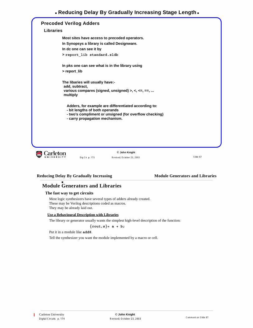
Precoded Verilog Adders
Libraries
Most sites have access to precoded operators.
In Synopsys a library is called Designware.In dc one can see it by
> report_lib standard.sldb
In pks one can see what is in the library using
> report_lib
The libaries will usually have:-add, subtract,various compares (signed, unsigned) >, <, <=, ==, ...multiply
Adders, for example are differentiated according to:- bit lengths of both operands- two’s compliment or unsigned (for overflow checking)- carry propagation mechanism.
Slide 87
Carleton University © John KnightDigital Circuits p. 174 Revised; October 23, 2003
Reducing Delay By Gradually Increasing Module Generators and Libraries
Module Generators and LibrariesThe fast way to get circuits
Most logic synthesizers have several types of adders already created.These may be Verilog descriptions coded as macros.They may be already laid out.
Use a Behavioural Description with Libraries
The library or generator usually wants the simplest high-level description of the function:
{cout,s}= a + b;
Put it in a module like add8.
Tell the synthesizer you want the module implemented by a macro or cell.
Comment on Slide 87
Incrementers
© John Knight
Dig Cir p. 175 Revised; October 23, 2003
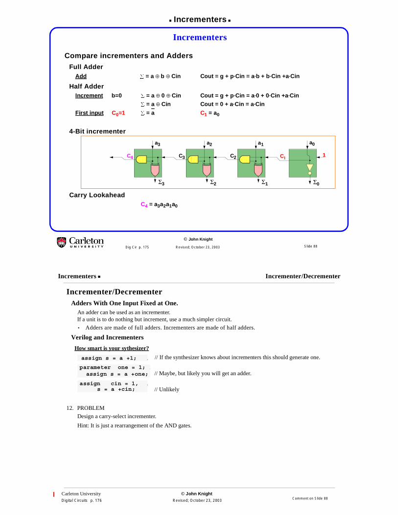
Incrementers
Compare incrementers and Adders
Full AdderAdd � = a ⊕ b ⊕ Cin Cout = g + p·Cin = a·b + b·Cin +a·Cin
Half AdderIncrement b=0 � = a ⊕ 0 ⊕ Cin Cout = g + p·Cin = a·0 + 0·Cin +a·Cin
� = a ⊕ Cin Cout = 0 + a·Cin = a·Cin
First input C0=1 � = a C1 = a0
4-Bit incrementer
Carry LookaheadC4 = a3a2a1a0
Σ1
C1
a1
C2
Σ0
1
a0
Σ2
a2
C3
Σ3
a3
C4
Slide 88
Carleton University © John KnightDigital Circuits p. 176 Revised; October 23, 2003
Incrementers Incrementer/Decrementer
Incrementer/DecrementerAdders With One Input Fixed at One.
An adder can be used as an incrementer.If a unit is to do nothing but increment, use a much simpler circuit.
• Adders are made of full adders. Incrementers are made of half adders.
Verilog and Incrementers
How smart is your sythesizer?
// If the synthesizer knows about incrementers this should generate one.
// Maybe, but likely you will get an adder.
// Unlikely
12. PROBLEM
Design a carry-select incrementer.
Hint: It is just a rearrangement of the AND gates.
assign s = a +1;
assign s = a +one;parameter one = 1;
s = a +cin;assign cin = 1,
Comment on Slide 88
Incrementers
© John Knight
Dig Cir p. 177 Revised; October 23, 2003
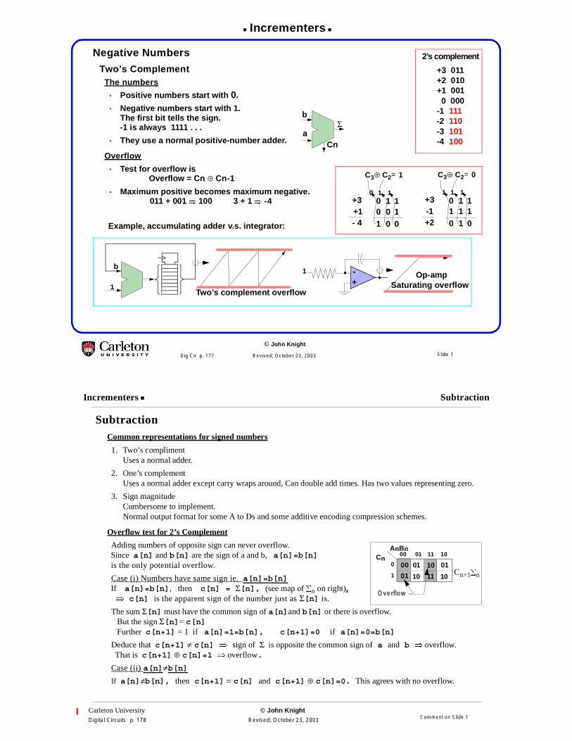
Negative Numbers
Two’s ComplementThe numbers
• Positive numbers start with 0.• Negative numbers start with 1.
The first bit tells the sign.-1 is always 1111 . . .
• They use a normal positive-number adder.
Overflow
• Test for overflow isOverflow = Cn ⊕ Cn-1
• Maximum positive becomes maximum negative.011 + 001 � 100 3 + 1 � -4
Example, accumulating adder v.s. integrator:
2’s complement
+3 011+2 010+1 0010 000
-1 111-2 110-3 101-4 100
a
bΣ
Cn
0 1 1+31 1 10 1 0
11 1
-1+2
C3⊕ C2= 0
0 1 1+30 0 11 0 0
10 1
+1- 4
C3⊕ C2= 1
Saturating overflowOp-amp-
+
b
Two’s complement overflow
1
1
Slide 1
Carleton University © John KnightDigital Circuits p. 178 Revised; October 23, 2003
Incrementers Subtraction
SubtractionCommon representations for signed numbers
1. Two’s complimentUses a normal adder.
2. One’s complementUses a normal adder except carry wraps around, Can double add times. Has two values representing zero.
3. Sign magnitudeCumbersome to implement.Normal output format for some A to Ds and some additive encoding compression schemes.
Overflow test for 2’s Complement
Adding numbers of opposite sign can never overflow.Since a[n] and b[n] are the sign of a and b, a[n]=b[n]is the only potential overflow.
Case (i) Numbers have same sign ie. a[n]=b[n]If a[n]=b[n], then c[n] = Σ[n], (see map of �n on right).� c[n] is the apparent sign of the number just as Σ[n] is.
The sum Σ[n] must have the common sign of a[n]and b[n] or there is overflow.But the sign Σ[n]= c[n]Further c[n+1] = 1 if a[n]=1=b[n], c[n+1]=0 if a[n]=0=b[n]
Deduce that c[n+1] ≠ c[n] � sign of Σ is opposite the common sign of a and b � overflow.That is c[n+1] ⊕ c[n]=1 � overflow.
Case (ii) a[n]≠b[n]If a[n]≠b[n], then c[n+1] = c[n] and c[n+1] ⊕ c[n]=0. This agrees with no overflow.
010100
01
00 01 11 10
0
1
AnBnCn
10
11 1010Cn+1�n
Overflow
Comment on Slide 1
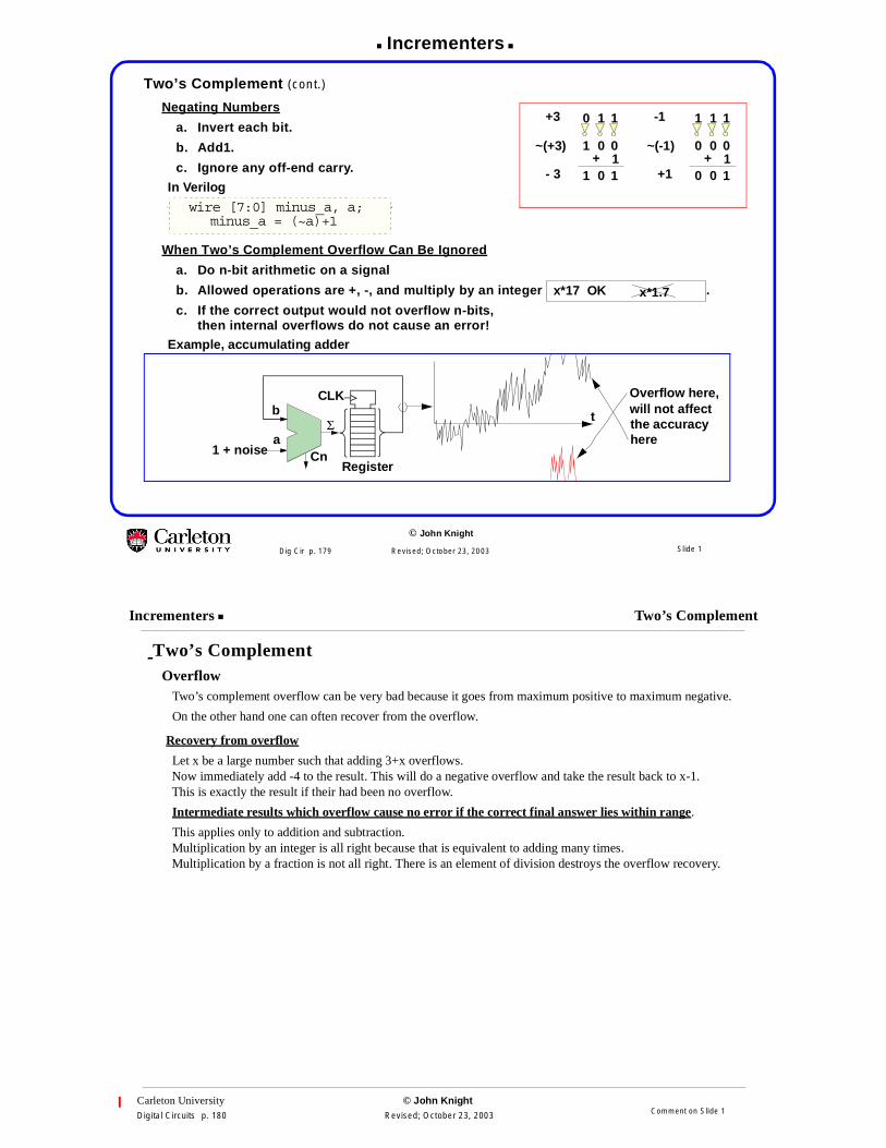
Incrementers
© John Knight
Dig Cir p. 179 Revised; October 23, 2003
Two’s Complement (cont.)
Negating Numbers
a. Invert each bit.
b. Add1.
c. Ignore any off-end carry.
In Verilog
When Two’s Complement Overflow Can Be Ignored
a. Do n-bit arithmetic on a signal
b. Allowed operations are +, -, and multiply by an integer .
c. If the correct output would not overflow n-bits,then internal overflows do not cause an error!
Example, accumulating adder
0 1 1+3
1 0 0
1 0 1
~(+3)
- 31+
1 1 1-1
0 0 0
0 0 1
~(-1)
+11+
wire [7:0] minus_a, a;minus_a = (~a)+1
x*17 OK x*1.7
Overflow here,will not affectthe accuracyhere
t
a
bΣ
Cn
CLK
Register1 + noise
Slide 1
Carleton University © John KnightDigital Circuits p. 180 Revised; October 23, 2003
Incrementers Two’s Complement
Two’s ComplementOverflow
Two’s complement overflow can be very bad because it goes from maximum positive to maximum negative.
On the other hand one can often recover from the overflow.
Recovery from overflow
Let x be a large number such that adding 3+x overflows.Now immediately add -4 to the result. This will do a negative overflow and take the result back to x-1.This is exactly the result if their had been no overflow.
Intermediate results which overflow cause no error if the correct final answer lies within range.
This applies only to addition and subtraction.Multiplication by an integer is all right because that is equivalent to adding many times.Multiplication by a fraction is not all right. There is an element of division destroys the overflow recovery.
Comment on Slide 1
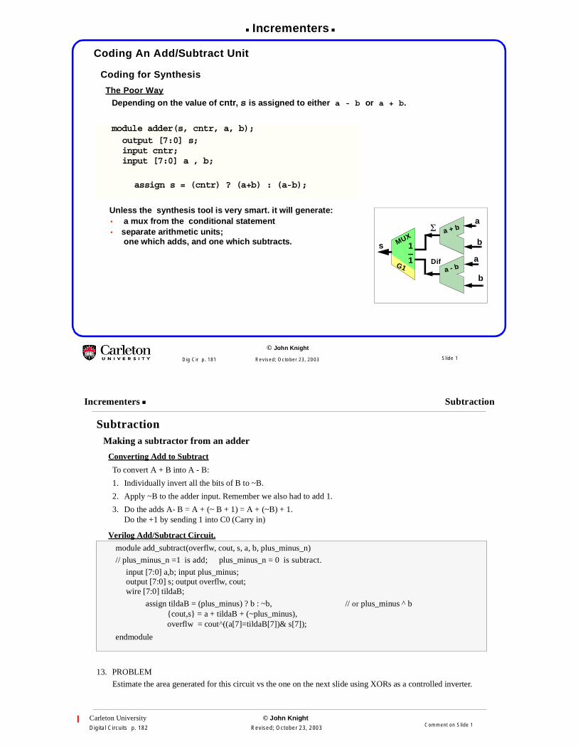
Incrementers
© John Knight
Dig Cir p. 181 Revised; October 23, 2003
Coding An Add/Subtract Unit
Coding for Synthesis
The Poor WayDepending on the value of cntr, s is assigned to either a - b or a + b.
Unless the synthesis tool is very smart. it will generate:• a mux from the conditional statement• separate arithmetic units;
one which adds, and one which subtracts.
module adder(s, cntr, a, b);output [7:0] s;input cntr;input [7:0] a , b;
assign s = (cntr) ? (a+b) : (a-b);
a
b
Σ
1
1G1
MUX
a
b
Difa - b
a + b
s
Slide 1
Carleton University © John KnightDigital Circuits p. 182 Revised; October 23, 2003
Incrementers Subtraction
SubtractionMaking a subtractor from an adder
Converting Add to Subtract
To convert A + B into A - B:
1. Individually invert all the bits of B to ~B.
2. Apply ~B to the adder input. Remember we also had to add 1.
3. Do the adds A- B = A + (~ B + 1) = A + (~B) + 1.Do the +1 by sending 1 into C0 (Carry in)
Verilog Add/Subtract Circuit.
13. PROBLEM
Estimate the area generated for this circuit vs the one on the next slide using XORs as a controlled inverter.
module add_subtract(overflw, cout, s, a, b, plus_minus_n)
// plus_minus_n =1 is add; plus_minus_n = 0 is subtract.
input [7:0] a,b; input plus_minus;output [7:0] s; output overflw, cout;wire [7:0] tildaB;
assign tildaB = (plus_minus) ? b : ~b, // or plus_minus ^ b{cout,s} = a + tildaB + (~plus_minus),overflw = cout^((a[7]=tildaB[7])& s[7]);
endmodule
Comment on Slide 1
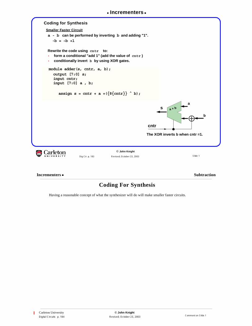
Incrementers
© John Knight
Dig Cir p. 183 Revised; October 23, 2003
Coding for Synthesis
Smaller Faster Circuit
a - b can be performed by inverting b and adding "1".-b = ~b +1
Rewrite the code using cntr to:• form a conditional "add 1" (add the value of cntr )• conditionally invert b by using XOR gates.
module adder(s, cntr, a, b);output [7:0] s;input cntr;input [7:0] a , b;
assign s = cntr + a +({8{cntr}} ^ b);
a
b
a + bs
cntr⊕
The XOR inverts b when cntr =1.
Slide 1
Carleton University © John KnightDigital Circuits p. 184 Revised; October 23, 2003
Incrementers Subtraction
Coding For Synthesis
Having a reasonable concept of what the synthesizer will do will make smaller faster circuits.
Comment on Slide 1
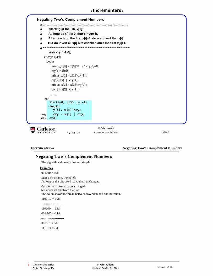
Incrementers
© John Knight
Dig Cir p. 185 Revised; October 23, 2003
Negating Two’s Complement Numbers// ...................................................................................................// Starting at the lsb, x[0]:
// As long as x[i] is 0, don’t invert it.// After reaching the first x[i]=1, do not invert that x[i].
// But do invert all x[i] bits checked after the first x[i]=1.
// ~~~~~~~~~~~~~~~~~~~~~~~~~~~~~~~~~~~~~~~~~~~~~~~~wire cry[n-1:0];
always @(x)
begin
minus_x[0] = x[0]^0 / / cry[0]=0;
cry[1]=x[0];
minus_x[1] = x[1]^cry[1] ;
cry[2]=x[1] | cry[1];
minus_x[2] = x[2]^cry[2] ;
cry[3]=x[2] | cry[2];
. . .
end
reg [N-1:0] y;wire [N-1:0] x;
for(i=0; i<N; i=i+1)
y[i]= x[i]^cry;cry = x[i] | cry;
begin
end
Slide 1
Carleton University © John KnightDigital Circuits p. 186 Revised; October 23, 2003
Incrementers Negating Two’s Complement Numbers
Negating Two’s Complement NumbersThe algorithm shown is fast and simple.
Examples
001010 = 10d
Start on the right, travel left.As long as the bits are 0 leave them unchanged.
On the first 1 leave that unchanged,but invert all bits from then on.The colon shows the break between inversion and noninversion.
1101:10 =-10d
----------------------
110100 =-12d
001:100 =-12d
----------------------
000101 = 5d
11101:1 =-5d
Comment on Slide 1


![< D q0 ] ª. !.J0¬+U C ¢/p](https://img.pdfslide.us/doc/110x75/618064c66710b66d94543d17/lt-d-q0-j0u-c-p.jpg)

![[1] 00mGJ Q0 0(!J@@ 00](https://img.pdfslide.us/doc/110x75/586e51b91a28abdd018ba3e2/1-00mgj-q0-0j-00.jpg)