Embed Size (px)
Citation preview

1Mbit – 16Mbit SPI (1-1-1) P-SRAM Memory
R e v i s i o n : I A v a l a n c h e T e c h n o l o g y P a g e 1 | 33
Ultra-Low Power Serial
Persistent SRAM Memory (AS1001101, AS1004101, AS1008101, AS1016101,
AS3001101, AS3004101, AS3008101, AS3016101)
Features
Interface
Serial Peripheral Interface SPI (1-1-1)
Technology
40nm pMTJ STT-MRAM
Data Endurance: 1016 write cycles
Data Retention: 20 years @ 85°C
Density
1Mb, 4Mb, 8Mb, 16Mb
Operating Voltage Range
VCC: 1.71V – 2.00V
VCC: 2.70V – 3.60V
Operating Temperature Range
Industrial: -40°C to 85°C
Industrial Plus: -40°C to 105°C
RoHS Compliant
Packages
8-pad WSON (5.0mm x 6.0mm)
8-pin SOIC (5.2mm x 5.2mm)
Data Protection
Hardware Based
Write Protect Pin (WP#)
Software Based
Address Range Selectable through
Configuration bits (Top/Bottom, Block
Protect[2:0])
Identification
64-bit Unique ID
64-bit User Programmable Serial Number
Augmented Storage Array
256-byte User Programmable and Lockable
Supports HOLD# Functionality - Pause
Performance
Device Operation Typical Values Units
Frequency of Operation 10.0 (maximum) MHz
Standby Current (Commercial) 1.3 (typical) µA
Active Current (Commercial) 1.8 (typical) mA

1Mbit – 16Mbit SPI (1-1-1) P-SRAM Memory
R e v i s i o n : I A v a l a n c h e T e c h n o l o g y P a g e 2 | 33
Table of Contents
Features ...................................................................................................................................................... 1
Performance .............................................................................................................................................. 1
Table of Contents ..................................................................................................................................... 2
General Description ................................................................................................................................. 4
Ordering Options ..................................................................................................................................... 5
Valid Combinations — Standard ...................................................................................................... 5
Signal Description and Assignment ................................................................................................. 12
Package Options .................................................................................................................................... 13
8-Pad WSON (Top View) ................................................................................................................... 13
8-Pin SOIC (Top View) ....................................................................................................................... 13
Package Drawings ................................................................................................................................. 14
8-Pad WSON ........................................................................................................................................ 14
8-Pin SOIC ............................................................................................................................................ 15
Architecture ............................................................................................................................................. 16
Device Initialization ............................................................................................................................... 17
Memory Map ............................................................................................................................................ 19
Augmented Storage Array Map .......................................................................................................... 19
Register Map ........................................................................................................................................... 20
Status Register / Device Protection Register (Read/Write) ........................................................... 20
Status register is a legacy SPI register and contains options for enabling/disabling data
protection. .............................................................................................................................................. 20
Device Identification Register (Read Only) ...................................................................................... 22
Serial Number Register (Read/Write) ............................................................................................... 22
Unique Identification Register (Read Only) ...................................................................................... 22
Instruction Set......................................................................................................................................... 23
Instruction Description and Structures ............................................................................................ 24
Electrical Specifications ....................................................................................................................... 26
CS# Operation & Timing ................................................................................................................... 28
Command, Address and Data Input Operation & Timing ........................................................ 29
Data Output Operation & Timing .................................................................................................... 30

1Mbit – 16Mbit SPI (1-1-1) P-SRAM Memory
R e v i s i o n : I A v a l a n c h e T e c h n o l o g y P a g e 3 | 33
WP# Operation & Timing .................................................................................................................. 31
HOLD# Operation & Timing ............................................................................................................. 32
Product Use Limitations ....................................................................................................................... 33
Limited Warranty ................................................................................................................................ 33

1Mbit – 16Mbit SPI (1-1-1) P-SRAM Memory
R e v i s i o n : I A v a l a n c h e T e c h n o l o g y P a g e 4 | 33
General Description ASxxxx101 is a magneto-resistive random-access memory (MRAM). It is offered in density ranging from
1Mbit to 16Mbit. MRAM technology is analogous to Flash technology with SRAM compatible read/write
timings (Persistent SRAM, P-SRAM). Data is always non-volatile with 1016 write cycles endurance and
greater than 20-year retention.
Figure 1: Technology Comparison
SRAM Flash EEPROM MRAM
Non-Volatility − √ √ √
Write Performance √ − − √
Read Performance √ − − √
Endurance √ − − √
Power − − − √
MRAM is a true random-access memory; allowing both reads and writes to occur randomly in memory. MRAM is ideal for applications that must store and retrieve data without incurring large latency penalties. It offers low latency, low power, infinite endurance and scalable non-volatile memory technology. ASxxxx101 has a Serial Peripheral Interface (SPI). SPI is a synchronous interface which uses separate lines for data and clock to help keep the host and slave in perfect synchronization. The clock tells the receiver exactly when to sample the bits on the data line. This can be either the rising (Low to High) or falling (High to Low) edge of the clock signal; please consult the instruction sequences in this datasheet for more details. When the receiver detects that correct edge, it can latch in the data. ASxxxx101 is available in small footprint 8-pad WSON and 8-pin SOIC packages. These packages are compatible with similar low-power volatile and non-volatile products. ASxxxx101 is offered with industrial (-40°C to 85°C) and industrial plus (-40°C to 105°C) operating temperature ranges.

1Mbit – 16Mbit SPI (1-1-1) P-SRAM Memory
R e v i s i o n : I A v a l a n c h e T e c h n o l o g y P a g e 5 | 33
Ordering Options The ordering part numbers are formed by a valid combination of the following options:
A 001 1 01 0010 X SA Y
Packing TypeR: Tape & Reel
Y: Tray
Temperature Range
0I: -40°C to +85°C
0P: -40°C to +105°C
Package TypeSA: 8-pin SOIC
WA: 8-pad WSON
Performance0001: 1MHz
0005: 5MHz
0010: 10Mhz
Interface Type1: Serial Peripheral Interface (SPI-SDR)
Density
001: 1 Megabit
004: 4 Megabit
008: 8 Megabit
016: 16 Megabit
Operational Voltage1: 1.8V (1.71V to 2.0V)
3: 3.0V (2.70V to 3.60V)
Product FamilyS: Persistent SRAM (P-SRAM)
BrandA: Avalanche Technology
S 3 - 0C
Sub-Interface Type
01: x1 (1-1-1) – Single SPI
Reserved
Valid Combinations — Standard Valid Combinations list includes device configurations currently available. Contact your local sales office to
confirm availability of specific valid combinations and to check on newly released combinations.

1Mbit – 16Mbit SPI (1-1-1) P-SRAM Memory
R e v i s i o n : I A v a l a n c h e T e c h n o l o g y P a g e 6 | 33
Table 1: Valid Combinations List
Valid Combinations – 1MHz
Base Part Number Temperature
Range Package Type
Packing Type
Part Number
AS1001101-0001X 0I, 0P SA, WA R, Y AS1001101-0001X0ISAR
AS1001101-0001X0ISAY
AS1001101-0001X0PSAR
AS1001101-0001X0PSAY
AS1001101-0001X0IWAR
AS1001101-0001X0IWAY
AS1001101-0001X0PWAR
AS1001101-0001X0PWAY
AS1004101-0001X 0I, 0P SA, WA R, Y AS1004101-0001X0ISAR
AS1004101-0001X0ISAY
AS1004101-0001X0PSAR
AS1004101-0001X0PSAY
AS1004101-0001X0IWAR
AS1004101-0001X0IWAY
AS1004101-0001X0PWAR
AS1004101-0001X0PWAY
AS1008101-0001X 0I, 0P SA, WA R, Y AS1008101-0001X0ISAR
AS1008101-0001X0ISAY
AS1008101-0001X0PSAR
AS1008101-0001X0PSAY
AS1008101-0001X0IWAR
AS1008101-0001X0IWAY
AS1008101-0001X0PWAR
AS1008101-0001X0PWAY
AS1016101-0001X 0I, 0P SA, WA R, Y AS1016101-0001X0ISAR
AS1016101-0001X0ISAY
AS1016101-0001X0PSAR
AS1016101-0001X0PSAY
AS1016101-0001X0IWAR
AS1016101-0001X0IWAY
AS1016101-0001X0PWAR
AS1016101-0001X0PWAY
AS3001101-0001X 0I, 0P SA, WA R, Y AS3001101-0001X0ISAR
AS3001101-0001X0ISAY
AS3001101-0001X0PSAR

1Mbit – 16Mbit SPI (1-1-1) P-SRAM Memory
R e v i s i o n : I A v a l a n c h e T e c h n o l o g y P a g e 7 | 33
AS3001101-0001X0PSAY
AS3001101-0001X0IWAR
AS3001101-0001X0IWAY
AS3001101-0001X0PWAR
AS3001101-0001X0PWAY
AS3004101-0001X 0I, 0P SA, WA R, Y AS3004101-0001X0ISAR
AS3004101-0001X0ISAY
AS3004101-0001X0PSAR
AS3004101-0001X0PSAY
AS3004101-0001X0IWAR
AS3004101-0001X0IWAY
AS3004101-0001X0PWAR
AS3004101-0001X0PWAY
AS3008101-0001X 0I, 0P SA, WA R, Y AS3008101-0001X0ISAR
AS3008101-0001X0ISAY
AS3008101-0001X0PSAR
AS3008101-0001X0PSAY
AS3008101-0001X0IWAR
AS3008101-0001X0IWAY
AS3008101-0001X0PWAR
AS3008101-0001X0PWAY
AS3016101-0001X 0I, 0P SA, WA R, Y AS3016101-0001X0CSAR
AS3016101-0001X0CSAY
AS3016101-0001X0ISAR
AS3016101-0001X0ISAY
AS3016101-0001X0PSAR
AS3016101-0001X0PSAY
AS3016101-0001X0CWAR
AS3016101-0001X0CWAY
AS3016101-0001X0IWAR
AS3016101-0001X0IWAY
AS3016101-0001X0PWAR
AS3016101-0001X0PWAY
Valid Combinations – 5MHz
Base Part Number Temperature
Range Package Type
Packing Type
Part Number
AS1001101-0005X 0I, 0P SA, WA R, Y AS1001101-0005X0ISAR
AS1001101-0005X0ISAY
AS1001101-0005X0PSAR
AS1001101-0005X0PSAY
AS1001101-0005X0IWAR
AS1001101-0005X0IWAY
AS1001101-0005X0PWAR

1Mbit – 16Mbit SPI (1-1-1) P-SRAM Memory
R e v i s i o n : I A v a l a n c h e T e c h n o l o g y P a g e 8 | 33
AS1001101-0005X0PWAY
AS1004101-0005X 0I, 0P SA, WA R, Y AS1004101-0005X0ISAR
AS1004101-0005X0ISAY
AS1004101-0005X0PSAR
AS1004101-0005X0PSAY
AS1004101-0005X0IWAR
AS1004101-0005X0IWAY
AS1004101-0005X0PWAR
AS1004101-0005X0PWAY
AS1008101-0005X 0I, 0P SA, WA R, Y AS1008101-0005X0ISAR
AS1008101-0005X0ISAY
AS1008101-0005X0PSAR
AS1008101-0005X0PSAY
AS1008101-0005X0IWAR
AS1008101-0005X0IWAY
AS1008101-0005X0PWAR
AS1008101-0005X0PWAY
AS1016101-0005X 0I, 0P SA, WA R, Y AS1016101-0005X0ISAR
AS1016101-0005X0ISAY
AS1016101-0005X0PSAR
AS1016101-0005X0PSAY
AS1016101-0005X0IWAR
AS1016101-0005X0IWAY
AS1016101-0005X0PWAR
AS1016101-0005X0PWAY
AS3001101-0005X 0I, 0P SA, WA R, Y AS3001101-0005X0ISAY
AS3001101-0005X0PSAR
AS3001101-0005X0PSAY
AS3001101-0005X0IWAR
AS3001101-0005X0IWAY
AS3001101-0005X0PWAR
AS3001101-0005X0PWAY
AS3004101-0005X 0I, 0P SA, WA R, Y AS3004101-0005X0ISAR
AS3004101-0005X0ISAY
AS3004101-0005X0PSAR
AS3004101-0005X0PSAY
AS3004101-0005X0IWAR
AS3004101-0005X0IWAY
AS3004101-0005X0PWAR
AS3004101-0005X0PWAY
AS3008101-0005X 0I, 0P SA, WA R, Y AS3008101-0005X0ISAR

1Mbit – 16Mbit SPI (1-1-1) P-SRAM Memory
R e v i s i o n : I A v a l a n c h e T e c h n o l o g y P a g e 9 | 33
AS3008101-0005X0ISAY
AS3008101-0005X0PSAR
AS3008101-0005X0PSAY
AS3008101-0005X0IWAR
AS3008101-0005X0IWAY
AS3008101-0005X0PWAR
AS3008101-0005X0PWAY
AS3016101-0005X 0I, 0P SA, WA R, Y AS3016101-0005X0ISAR
AS3016101-0005X0ISAY
AS3016101-0005X0PSAR
AS3016101-0005X0PSAY
AS3016101-0005X0IWAR
AS3016101-0005X0IWAY
AS3016101-0005X0PWAR
AS3016101-0005X0PWAY
Valid Combinations – 10MHz
Base Part Number Temperature
Range Package Type
Packing Type
Part Number
AS1001101-0010X 0I, 0P SA, WA R, Y AS1001101-0010X0ISAR
AS1001101-0010X0ISAY
AS1001101-0010X0PSAR
AS1001101-0010X0PSAY
AS1001101-0010X0IWAR
AS1001101-0010X0IWAY
AS1001101-0010X0PWAR
AS1001101-0010X0PWAY
AS1004101-0010X 0I, 0P SA, WA R, Y AS1004101-0010X0ISAR
AS1004101-0010X0ISAY
AS1004101-0010X0PSAR
AS1004101-0010X0PSAY
AS1004101-0010X0IWAR
AS1004101-0010X0IWAY
AS1004101-0010X0PWAR
AS1004101-0010X0PWAY
AS1008101-0010X 0C, 0I, 0P SA, WA R, Y AS1008101-0010X0CSAR
AS1008101-0010X0CSAY
AS1008101-0010X0ISAR
AS1008101-0010X0ISAY
AS1008101-0010X0PSAR
AS1008101-0010X0PSAY
AS1008101-0010X0CWAR
AS1008101-0010X0CWAY

1Mbit – 16Mbit SPI (1-1-1) P-SRAM Memory
R e v i s i o n : I A v a l a n c h e T e c h n o l o g y P a g e 10 | 33
AS1008101-0010X0IWAR
AS1008101-0010X0IWAY
AS1008101-0010X0PWAR
AS1008101-0010X0PWAY
AS1016101-0010X 0I, 0P SA, WA R, Y AS1016101-0010X0ISAR
AS1016101-0010X0ISAY
AS1016101-0010X0PSAR
AS1016101-0010X0PSAY
AS1016101-0010X0IWAR
AS1016101-0010X0IWAY
AS1016101-0010X0PWAR
AS1016101-0010X0PWAY
AS3001101-0010X 0I, 0P SA, WA R, Y AS3001101-0010X0ISAR
AS3001101-0010X0ISAY
AS3001101-0010X0PSAR
AS3001101-0010X0PSAY
AS3001101-0010X0IWAR
AS3001101-0010X0IWAY
AS3001101-0010X0PWAR
AS3001101-0010X0PWAY
AS3004101-0010X 0I, 0P SA, WA R, Y AS3004101-0010X0ISAR
AS3004101-0010X0ISAY
AS3004101-0010X0PSAR
AS3004101-0010X0PSAY
AS3004101-0010X0IWAR
AS3004101-0010X0IWAY
AS3004101-0010X0PWAR
AS3004101-0010X0PWAY
AS3008101-0010X 0I, 0P SA, WA R, Y AS3008101-0010X0ISAR
AS3008101-0010X0ISAY
AS3008101-0010X0PSAR
AS3008101-0010X0PSAY
AS3008101-0010X0IWAR
AS3008101-0010X0IWAY
AS3008101-0010X0PWAR
AS3008101-0010X0PWAY
AS3016101-0010X 0C, 0I, 0P SA, WA R, Y AS3016101-0010X0ISAR
AS3016101-0010X0ISAY
AS3016101-0010X0PSAR
AS3016101-0010X0PSAY
AS3016101-0010X0IWAR
AS3016101-0010X0IWAY

1Mbit – 16Mbit SPI (1-1-1) P-SRAM Memory
R e v i s i o n : I A v a l a n c h e T e c h n o l o g y P a g e 11 | 33
AS3016101-0010X0PWAR
AS3016101-0010X0PWAY

1Mbit – 16Mbit SPI (1-1-1) P-SRAM Memory
R e v i s i o n : I A v a l a n c h e T e c h n o l o g y P a g e 12 | 33
Signal Description and Assignment
Figure 2: Device Pinout
1Mb – 16Mb
Serial (SPI)
P-SRAM
CS#
WP#
SI
CLK
HOLD#
SO
Table 2: Signal Description
Signal Type Description
CS# Input
Chip Select: When CS# is driven High, the device will enter standby mode. All other input pins are ignored and the output pin is tri-stated. Driving CS# Low enables the device, placing it in the active mode. After power-up, a falling edge on CS# is required prior to the start of any instructions.
WP# Input
Write Protect: Write protects the status register in conjunction with the enable/disable bit of the status register. This is important since other write protection features are controlled through the Status Register. When the enable/disable bit of the status register is set to 1 and the WP# signal is driven Low, the status register becomes read-only and the WRITE STATUS REGISTER operation will not execute. This signal does not have internal pull-ups, it cannot be left floating and must be driven.
CLK Input
Clock: Provides the timing of the serial interface. Command, address and data inputs are latched on the rising edge of the clock. Data is output on the falling edge of the clock. The following two SPI clock modes are supported.
SPI Mode 0 (CPOL = 0, CPHA = 0)
SPI Mode 3 (CPOL = 1, CPHA = 1)
HOLD# Input Hold: Pauses serial communications with the device without deselecting or resetting the device. Outputs are tri-stated and inputs are ignored.
SI Input Serial Data Input: The unidirectional I/O transfers data into the device on the rising edge of the clock.
SO Output Serial Data Output: The unidirectional I/O transfers data out of the device on the falling edge of the clock.
VCC Supply VCC: Core and I/O power supply.
VSS Supply VSS: Core and I/O ground supply.

1Mbit – 16Mbit SPI (1-1-1) P-SRAM Memory
R e v i s i o n : I A v a l a n c h e T e c h n o l o g y P a g e 13 | 33
Package Options
8-Pad WSON (Top View) Figure 3: 8-Pad WSON
1
2
3
4
8
7
6
5
CS#
WP#
SI
CLK
HOLD#SO
VCC
VSS
8-Pin SOIC (Top View) Figure 4: 8-Pin SOIC
1
2
3
4
8
7
6
5
CS#
WP#
SI
CLK
HOLD#SO
VCC
VSS

1Mbit – 16Mbit SPI (1-1-1) P-SRAM Memory
R e v i s i o n : I A v a l a n c h e T e c h n o l o g y P a g e 14 | 33
Package Drawings
8-Pad WSON

1Mbit – 16Mbit SPI (1-1-1) P-SRAM Memory
R e v i s i o n : I A v a l a n c h e T e c h n o l o g y P a g e 15 | 33
8-Pin SOIC

1Mbit – 16Mbit SPI (1-1-1) P-SRAM Memory
R e v i s i o n : I A v a l a n c h e T e c h n o l o g y P a g e 16 | 33
Architecture ASxxxx101 is an ultra-low power serial STT-MRAM device. It features a SPI-compatible bus interface, execute-in-place (XIP) functionality, and hardware/software based data protection mechanisms. When CS# is Low, the device is selected and in active power mode. When CS# is High, the device is deselected but can remain in active power mode until ongoing internal operations are completed. Then the device goes into standby power mode and device current consumption drops to ISB. ASxxxx101 contains an 8-bit instruction register. All functionality is controlled through the values loaded into this instruction register. The device is accessed via the SI pin, with data being clocked in on the rising edge of CLK - CS# pin must be Low and the HOLD# pin must be High for the entire operation. If the clock line is shared with other peripheral devices on the SPI bus, the user can assert the HOLD# input and place ASxxxx101 in ‘HOLD’ state. After releasing the HOLD# pin, operation will resume from the point when the HOLD# was asserted. ASxxxx101 has a 256-byte Augmented Storage Array which is independent from the main memory array. It is user programmable and can be locked against inadvertent writes. The device offers both hardware and software based data protection schemes. Hardware protection is through WP# pin. Software protection is controlled by configuration bits in the Status register. Both schemes inhibit writing to the memory array.
Figure 5: Functional Block Diagram
Regulator
MRAM
ArrayMRAM
ArrayCommand
&
Control
MRAM
Array
Row
De
co
de
r
Column
Decoder
Data Buffer
Serial
I/Os
Address Register
Status Register
Command Register
High Voltage
Generator
CS#
WP#
SI
CLK
HOLD#SO
VCC
VSS
Table 3: Modes of Operation
Mode CS# Current SI SO HOLD#
Standby H ISB Gated Hi-Z Gated
Active - Read L IREAD Instruction Dataout H
Active - Write L IWRITE Instruction, Datain Hi-Z H
Hold L IREAD, IWRITE Not Gated FD L
Notes:
H: High (Logic ‘1’)
L: Low (Logic ‘0’)
Hi-Z: High Impedance

1Mbit – 16Mbit SPI (1-1-1) P-SRAM Memory
R e v i s i o n : I A v a l a n c h e T e c h n o l o g y P a g e 17 | 33
Device Initialization When powering up, the following procedure is required to initialize the device correctly:
Ramp up VCC (RVR)
CS# must follow VCC during power-up (a 10KΩ pull-up Resistor to VCC is recommended)
It is recommended that no instructions are sent to the device when VCC is below VCC (minimum)
During initial Power-up, recovering from power loss or brownout, a delay of tPU is required before normal operation commences
Upon Power-up, the device is in Standby mode
Figure 6: Power-Up Behavior
VCC
(Minimum)
VCC
(Maximum)
Voltage
Time
tPU
0V
Device
Fully
Operational
When powering down, the following procedure is required to turn off the device correctly:
Ramp down VCC (RVF)
CS# must follow VCC during power-down (a 10KΩ pull-up Resistor to VCC is recommended)
It is recommended that no instructions are sent to the device when VCC is below VCC (minimum)
The Power-up timing needs to be observed after VCC goes above VCC (minimum)
Figure 7: Power-Down Behavior
VCC
(Minimum)
VCC
(Maximum)
Voltage
Time0V
Device
Fully
Operational
VCC-CUTOFF
(Cut Off)
tPU

1Mbit – 16Mbit SPI (1-1-1) P-SRAM Memory
R e v i s i o n : I A v a l a n c h e T e c h n o l o g y P a g e 18 | 33
Table 4: Device Initialization Timing
Parameter Symbol Test Conditions 3.0V
Minimum Typical Maximum Units
VCC Range All operating voltages and temperatures
2.7 - 3.6 V
VCC Ramp Up Time RVR All operating voltages and temperatures
30 - - µs/V
VCC Ramp Down Time RVF All operating voltages and temperatures
20 - - µs/V
VCC Power Up to First Instruction tPU All operating voltages and temperatures
250 - - µs
VCC Cutoff – Must Initialize Device VCC-CUTOFF All operating voltages and temperatures
1.6 - - V
Table 5: Device Initialization Timing – 1.8V
Parameter Symbol Test Conditions 1.8V
Minimum Typical Maximum Units
VCC Range All operating voltages and temperatures
1.71 - 2.0 V
VCC Ramp Up Time RVR All operating voltages and temperatures
30 - - µs/V
VCC Ramp Down Time RVF All operating voltages and temperatures
20 - - µs/V
VCC Power Up to First Instruction tPU All operating voltages and temperatures
250 - - µs
VCC Cutoff – Must Initialize Device VCC-CUTOFF All operating voltages and temperatures
1.6 - - V

1Mbit – 16Mbit SPI (1-1-1) P-SRAM Memory
R e v i s i o n : I A v a l a n c h e T e c h n o l o g y P a g e 19 | 33
Memory Map Table 6: Memory Map
Density Address Range 24-bit Address [23:0]
1Mb 000000h – 01FFFFh [23:17] – Logic ‘0’ [16:0] - Addressable
4Mb 000000h – 07FFFFh [23:19] – Logic ‘0’ [18:0] - Addressable
8Mb 000000h – 0FFFFFh [23:20] – Logic ‘0’ [19:0] - Addressable
16Mb 000000h – 1FFFFFh [23:21] – Logic ‘0’ [20:0] - Addressable
Augmented Storage Array Map
Table 7: Augmented Storage Array Map
Density Address Range 24-bit Address [23:0]
1Mb 002000h – 0020FFh 1 [23:14] – Logic ‘0’, [13] – Logic ‘1’, [12:8] – Logic ‘0’ [7:0] - Addressable
4Mb 002000h – 0020FFh 1 [23:14] – Logic ‘0’, [13] – Logic ‘1’, [12:8] – Logic ‘0’ [7:0] - Addressable
8Mb 002000h – 0020FFh 1 [23:14] – Logic ‘0’, [13] – Logic ‘1’, [12:8] – Logic ‘0’ [7:0] - Addressable
16Mb 002000h – 0020FFh 1 [23:14] – Logic ‘0’, [13] – Logic ‘1’, [12:8] – Logic ‘0’ [7:0] - Addressable

1Mbit – 16Mbit SPI (1-1-1) P-SRAM Memory
R e v i s i o n : I A v a l a n c h e T e c h n o l o g y P a g e 20 | 33
Register Map
Status Register / Device Protection Register (Read/Write)
Status register is a legacy SPI register and contains options for enabling/disabling data protection.
Table 8: Status Register
Bits Name Description Read
/ Write
Default State
Selection Options
SR[7] WP#EN Hardware Based WP# Protection Enable/Disable
R/W 0
1: Protection Enabled – write protects when WP# is Low 0: Protection Disabled – Doesn’t write protect when WP# is Low
SR[6] SNPEN Serial Number Protection Enable/Disable
R/W 0 1: S/N Write protected - protection enabled 0: S/N Writable - protection disabled
SR[5] TBPSEL Software Top/Bottom Memory Array Protection Selection
R/W 0
1: Bottom Protection Enabled (Lower Address Range) 0: Top Protection Enabled (Higher Address Range)
SR[4] BPSEL[2] Block Protect Selection Bit 2 R/W 0 Block Protection Bits SR[3] BPSEL[1] Block Protect Selection Bit 1 R/W 0
SR[2] BPSEL[0] Block Protect Selection Bit 0 R/W 0
SR[1] WREN Write Operation Enable/Disable
R 0 1: Write Operation Enabled 0: Write Operation Disabled
SR[0] RSVD Reserved R 0 Reserved for future use
Table 9: Top Block Protection Address Range Selection (TBPSEL=0)
BPSEL [2]
BPSEL [1]
BPSEL [0]
Protected Portion
1Mb 4Mb 8Mb 16Mb
0 0 0 None None None None None
0 0 1 Upper 1/64 01F800h – 01FFFFh
07E000h – 07FFFFh
0FC000h – 0FFFFFh
1F8000h – 1FFFFFh
0 1 0 Upper 1/32 01F000h – 01FFFFh
07C000h – 07FFFFh
0F8000h – 0FFFFFh
1F0000h – 1FFFFFh
0 1 1 Upper 1/16 01E000h – 01FFFFh
078000h – 07FFFFh
0F0000h – 0FFFFFh
1E0000h – 1FFFFFh
1 0 0 Upper 1/8 01C000h – 01FFFFh
070000h – 07FFFFh
0E0000h – 0FFFFFh
1C0000h – 1FFFFFh
1 0 1 Upper 1/4 018000h – 01FFFFh
060000h – 07FFFFh
0C0000h – 0FFFFFh
180000h – 1FFFFFh
1 1 0 Upper 1/2 010000h – 01FFFFh
040000h – 07FFFFh
080000h – 0FFFFFh
1F0000h – 1FFFFFh
1 1 1 All 000000h – 01FFFFh
000000h – 07FFFFh
000000h – 0FFFFFh
000000h – 1FFFFFh

1Mbit – 16Mbit SPI (1-1-1) P-SRAM Memory
R e v i s i o n : I A v a l a n c h e T e c h n o l o g y P a g e 21 | 33
Table 10: Bottom Block Protection Address Range Selection (TBPSEL=1)
BPSEL [2]
BPSEL [1]
BPSEL [0]
Protected Portion
1Mb 4Mb 8Mb 16Mb
0 0 0 None None None None None
0 0 1 Lower 1/64 000000h – 0007FFh
000000h – 001FFFh
000000h – 003FFFh
000000h – 007FFFh
0 1 0 Lower 1/32 000000h –
00FFFh 000000h – 003FFFh
000000h – 007FFFh
000000h – 00FFFFh
0 1 1 Lower 1/16 000000h – 001FFFh
000000h – 007FFFh
000000h – 00FFFFh
000000h – 01FFFFh
1 0 0 Lower 1/8 000000h – 003FFFh
000000h – 00FFFFh
000000h – 01FFFFh
000000h – 03FFFFh
1 0 1 Lower 1/4 000000h – 007FFFh
000000h – 01FFFFh
000000h – 03FFFFh
000000h – 07FFFFh
1 1 0 Lower 1/2 000000h – 00FFFFh
000000h – 03FFFFh
000000h – 07FFFFh
000000h – 0FFFFFh
1 1 1 All 000000h – 01FFFFh
000000h – 07FFFFh
000000h – 0FFFFFh
000000h – 1FFFFFh
Table 11: Write Protection Modes
WREN (Status Register)
WP#EN (Status Register)
WP# (Pin)
Status Register
Memory1 Array
Protected Area
Memory1 Array
Unprotected Area
0 X X Protected Protected Protected
1 0 X Unprotected Protected Unprotected
1 1 Low Protected Protected Unprotected
1 1 High Unprotected Protected Unprotected
Notes:
High: Logic ‘1’
Low: Logic ‘0’
X: Don’t Care – Can be Logic ‘0’ or ‘1’
Protected: Write protected
Unprotected: Writable
1: Memory address range protection based on Block Protection Bits

1Mbit – 16Mbit SPI (1-1-1) P-SRAM Memory
R e v i s i o n : I A v a l a n c h e T e c h n o l o g y P a g e 22 | 33
Device Identification Register (Read Only) Device identification register contains Avalanche’s Manufacturing ID along with device configuration
information.
Table 12: Device Identification Register – Read Only
Bits Avalanche
Manufacturer's ID Device
Configuration
ID[31:0] ID[31:24] Interface Voltage Temp Density Freq
ID[23:20] ID[19:16] ID[15:12] ID[11:8] ID[7:0]
Manufacturer ID
Interface Voltage Temperature Density Frequency
31-24 23-20 19-16 15-12 11-8 7-0
1110 0110 0001-ULP SPI 0001 - 3V 0000 - -40⁰C- 85⁰C 0001 - 1Mb 0110 - 1MHz
0010 - 1.8V 0001 - -40⁰C-105⁰C 0010 - 4Mb 0111 - 5MHz
0011 - 8Mb 1000 - 10MHz
0100 - 16Mb 1001 - 20MHz
Serial Number Register (Read/Write) Serial Number register is user writable.
Table 13: Serial Number Register – Read and Write
Bits Name Description Read
/ Write
Default State 1 Selection Options
SN[63:0] SN Serial Number Value R/W 000000000000
0000h Value stored is based on the customer
Unique Identification Register (Read Only) Unique Identification register contains a number unique to every device.
Table 14: Unique ID Register – Read Only
Bits Name Description Read / Write
Selection Options
UID[63:0] UID Unique Identification Number Value
R Value stored is written in the factory and is device specific

1Mbit – 16Mbit SPI (1-1-1) P-SRAM Memory
R e v i s i o n : I A v a l a n c h e T e c h n o l o g y P a g e 23 | 33
Instruction Set Table 15: Instruction Set
# Instruction
Name
Co
mm
an
d
(Op
co
de
)
1-0
-0
1-0
-1
1-1
-1
La
ten
cy C
ycle
s
Data
B
yte
s
Ad
dre
ss B
yte
s
Ma
x. F
req
ue
ncy
Pre
req
uis
ite
Control Instructions
1 No Operation NOOP - 00h • 0 10MHz
2 Write Enable WREN- 06h • 0 10MHz
3 Write Disable WRDI - 04h • 0 10MHz
4 Software Reset Enable SRTE - 66h • 0 10MHz
5 Software Reset SRST - 99h • 0 10MHz SRTE
Read Register Instructions
6 Read Status Register 3 RDSR - 05h • 1 0 10MHz
7 Read Device ID 3 RDID - 9Fh • 4 0 10MHz
8 Read Unique ID 3 RUID - 4Ch • 8 0 10MHz
9 Read Serial Number Register 3 RDSN - C3h • 8 0 10MHz
Write Register Instructions
10 Write Status Register WRSR - 01h • 1 0 10MHz WREN
11 Write Serial Number Register WRSN - C2h • 8 0 10MHz WREN
Read Memory Array Instructions
12 Read Memory Array READ - 03h •
1 to ∞ 3 10MHz
13 Fast Read Memory Array 4 RDFT - 0Bh • • 1 to ∞ 3 10MHz
Write Memory Array Instructions
14 Write Memory Array WRTE - 02h • 1 to ∞ 3 10MHz WREN
Augmented Storage Array Instructions
15 Read Augmented Storage Array RDAS - 4Bh • 1 to 256 32 10MHz
16 Write Augmented Storage Array WRAS - 42h • 1 to 256 32 10MHz WREN
Notes:
1: The command code for an instruction is always transmitted on SI according to the SPI standard. However, an instruction may
transmit address and data (send or receive) as well. The command-address-data column shows which of these three components the
instruction contains. As an example, READ instruction has command, address, and data information: 1-1-1. On the other hand, SRST
instruction only has command information: 1-0-0.
2: The augmented storage array is 256-Bytes in size.
3: Registers do not wrap data during reads. Reading beyond the specified number of bytes will yield indeterminate data.
4: Fast Read instruction requires 8 dummy CLK cycles after the address is entered and before the beginning of the read data. SI can
be driven High or Low or left floating during the dummy CLK cycles.
5: The Status register needs to be re-initialized after a solder reflow process. Refer to the application note for the detailed
description.

1Mbit – 16Mbit SPI (1-1-1) P-SRAM Memory
R e v i s i o n : I A v a l a n c h e T e c h n o l o g y P a g e 24 | 33
Instruction Description and Structures All communication between a host and ASxxxx101 is in the form of instructions. Instructions define the
operation that must be executed. Instructions consist of a command followed by an optional address
modifier and data transfer to or from ASxxxx101. All command, address and data information is transferred
sequentially. Instructions are structured as follows:
Each instruction begins with CS# going Low (logic ‘0’) and ends with CS# returning High (Logic’1’).
CLK marks the transfer of each bit.
Each instructions starts out with an 8-bit command. The command selects the type of operation
ASxxxx101 must perform. The command is transferred on the rising edges of CLK.
The command can be stand alone or followed by address to select a memory location. The address
is always 24-bits wide. The address is transferred on the rising edges of CLK.
The address bits are followed by data bits. Write data bits to ASxxxx101 are transferred on the
rising edges of CLK. Read data bits from ASxxxx101 are transferred on the falling edges of CLK.
Fast Read instruction (RDFT) requires 8 dummy CLK cycles after the address is entered and before
the beginning of the read data. The dummy clock cycles are latency cycles. SI is ignored by
ASxxxx101 during these dummy cycles.
Write instructions must be preceded by the WREN instruction. WREN instruction sets the WREN
bit in the Status register. WREN bit is reset at the end of every write instruction. WREN bit can also
be reset by executing the WRDI instruction.
The entire memory array can be read from or written to using a single read or write instruction. After
the staring address is entered, subsequent address are internally incremented as long as CS# is
Low and CLK continues to cycle.
All commands, address and data are shifted with the most significant bit first.
Figure 8 to Figure 11 shows the description of instruction types supported.

1Mbit – 16Mbit SPI (1-1-1) P-SRAM Memory
R e v i s i o n : I A v a l a n c h e T e c h n o l o g y P a g e 25 | 33
Figure 8: Description of (1-0-0) Instruction Type 1
Byte
CS#
SI
CLK03
7 6 5 4 3 2 1 0
Command
Figure 9: Description of (1-0-1) Instruction Type
1 to 8 Bytes
Read/Write
1Byte
CS#
SI / IO[0]
CLK03
7 6 5 4 3 2 1 0 7 6 5 4 2 1 0
7 6 5 4 2 1 0SO / IO[1]
Command Input Data
Output Data
Figure 10: Description of (1-1-1) Instruction Type (No Latency)
1 to Bytes
Read/Write
1Byte
CS#
SI / IO[0]
CLK03
7 6 5 4 3 2 1 0 7 6 5 4 2 1 0
7 6 5 4 2 1 0SO / IO[1]
Command Input Data
Output Data
7 6 5 4 2 1 0
Address
3Bytes
Figure 11: Description of (1-1-1) Instruction Type (With Latency)
1 to Bytes
1Byte
CS#
SI / IO[0]
CLK03
7 6 5 4 3 2 1 0
7 6 5 4 2 1 0SO / IO[1]
Command
Output Data
7 6 5 4 2 1 0
Address
3Bytes
8DummyCycles
Read
1Mbit – 16Mbit SPI (1-1-1) P-SRAM Memory
R e v i s i o n : I A v a l a n c h e T e c h n o l o g y P a g e 26 | 33
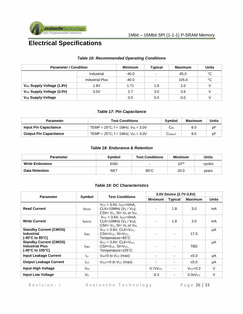
Electrical Specifications
Table 16: Recommended Operating Conditions
Parameter / Condition Minimum Typical Maximum Units
Industrial -40.0 - 85.0 °C
Industrial Plus -40.0 - 105.0 °C
VCC Supply Voltage (1.8V) 1.8V 1.71 1.8 2.0 V
VCC Supply Voltage (3.0V) 3.0V 2.7 3.0 3.6 V
VSS Supply Voltage 0.0 0.0 0.0 V
Table 17: Pin Capacitance
Parameter Test Conditions Symbol Maximum Units
Input Pin Capacitance TEMP = 25°C; f = 1MHz; VIN = 3.0V CIN 6.0 pF
Output Pin Capacitance TEMP = 25°C; f = 1MHz; VIN = 3.0V CINOUT 8.0 pF
Table 18: Endurance & Retention
Parameter Symbol Test Conditions Minimum Units
Write Endurance END - 1016 cycles
Data Retention RET 85°C 20.0 years
Table 19: DC Characteristics
Parameter Symbol Test Conditions 3.0V Device (2.7V-3.6V)
Minimum Typical Maximum Units
Read Current IREAD VCC = 3.6V, IOUT=0mA, CLK=10MHz (VIL / VIH), CS#= VIL, SI= VIL or VIH
- 1.8 3.0 mA
Write Current IWRITE VCC = 3.6V, IOUT=0mA, CLK=10MHz (VIL / VIH), CS#= VIL, SI= VIL or VIH
- 1.8 3.0 mA
Standby Current (CMOS) Industrial (-40°C to 85°C)
ISB2 VCC = 3.6V, CLK=VCC, CS#=VCC, SI=VCC, Temperature=85°C
- - 17.0 µA
Standby Current (CMOS) Industrial Plus (-40°C to 105°C)
ISB3 VCC = 3.6V, CLK=VCC, CS#=VCC, SI=VCC, Temperature=105°C
- - TBD µA
Input Leakage Current ILI VIN=0 to VCC (max) - - ±5.0 µA
Output Leakage Current ILO VOUT=0 to VCC (max) - - ±5.0 µA
Input High Voltage VIH 0.7xVCC - VCC+0.3 V
Input Low Voltage VIL -0.3 - 0.3xVCC V

1Mbit – 16Mbit SPI (1-1-1) P-SRAM Memory
R e v i s i o n : I A v a l a n c h e T e c h n o l o g y P a g e 27 | 33
Parameter Symbol Test Conditions 3.0V Device (2.7V-3.6V)
Minimum Typical Maximum Units
Output High Voltage Level VOH IOH = -100µA VCC-0.2 - - V
IOH = -1mA 2.4 - - V
Table 20: Magnetic Immunity Characteristics
Parameter Symbol Maximum Units
Magnetic Field During Write Hmax_write 24000 A/m
Magnetic Field During Read Hmax_read 24000 A/m
Table 21: AC Test Conditions
Parameter Value
Input Pulse Levels 0.0V to VCC
Input Rise and Fall Times 3.0ns
Input and Output Measurement Timing Levels VCC/2
Output Load CL = 30.0pF

1Mbit – 16Mbit SPI (1-1-1) P-SRAM Memory
R e v i s i o n : I A v a l a n c h e T e c h n o l o g y P a g e 28 | 33
CS# Operation & Timing
Figure 12: CS# Operation & Timing
CS#
tCS
CLK
tCSS
tCSH
tCSS
Table 22: CS# Operation
Parameter Symbol Minimum Maximum Units
Clock Frequency fCLK 1.0 10.0 MHz
Clock Low Time tCL 11.0 - ns
Clock High Time tCH 11.0 - ns
Chip Deselect Time after Status Register Write tCS1 3.0 - µs
Chip Deselect Time after SN Register Write tCS2 10.0 - µs
Chip Deselect Time after Memory Array Read / Write tCS3 40.0 - ns
CS# Setup Time (w.r.t CLK) tCSS 5.0 - ns
CS# Hold Time (w.r.t CLK) tCSH 5.0 - ns
Notes:
Power supplies must be stable

1Mbit – 16Mbit SPI (1-1-1) P-SRAM Memory
R e v i s i o n : I A v a l a n c h e T e c h n o l o g y P a g e 29 | 33
Command, Address and Data Input Operation & Timing
Figure 13: Command, Address and Data Input Operation & Timing
CS#
CLK
SI
Don t
Care
tSU
New Data
tHD
tCSS
Table 23: Command, Address and Data Input Operation & Timing
Parameter Symbol Minimum Maximum Units
Data Setup Time (w.r.t CLK) tSU 5.0 - ns
Data Hold Time (w.r.t CLK) tHD 5.0 - ns
Notes:
Power supplies must be stable

1Mbit – 16Mbit SPI (1-1-1) P-SRAM Memory
R e v i s i o n : I A v a l a n c h e T e c h n o l o g y P a g e 30 | 33
Data Output Operation & Timing
Figure 14: Data Output Operation & Timing
CS#
CLK
SO
Don t
Care
New Data 1
tCSS
tCO
tCLZ
New Data 2High-Z
tHZCStOH
tCSH
Table 24: Data Output Operation & Timing
Parameter Symbol Minimum Maximum Units
CLK Low to Output Low Z (Active) tCLZ 0 - ns
Output Valid (w.r.t CLK) tCO - 9.0 ns
Output Hold Time (w.r.t CLK) tOH 1.0 - ns
Output Disable Time (w.r.t CS#) tHZCS - 12 ns
Notes:
Power supplies must be stable
1Mbit – 16Mbit SPI (1-1-1) P-SRAM Memory
R e v i s i o n : I A v a l a n c h e T e c h n o l o g y P a g e 31 | 33
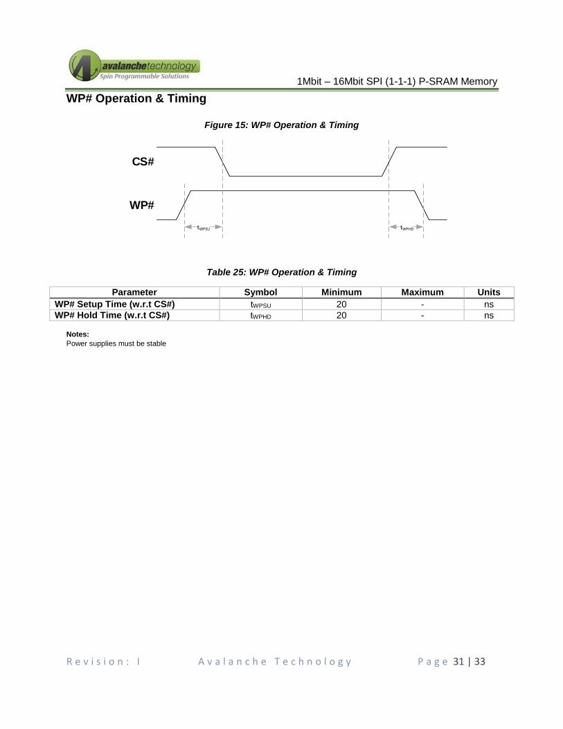
WP# Operation & Timing
Figure 15: WP# Operation & Timing
CS#
WP#
tWPSU tWPHD
Table 25: WP# Operation & Timing
Parameter Symbol Minimum Maximum Units
WP# Setup Time (w.r.t CS#) tWPSU 20 - ns
WP# Hold Time (w.r.t CS#) tWPHD 20 - ns
Notes:
Power supplies must be stable

1Mbit – 16Mbit SPI (1-1-1) P-SRAM Memory
R e v i s i o n : I A v a l a n c h e T e c h n o l o g y P a g e 32 | 33
HOLD# Operation & Timing
Figure 16: HOLD# Operation & Timing
CS#
tHLCH
CLK
tCHHL
HOLD#
SO Data 1 Data 1Data 0
tHHQX
Data 2
tHLQZ
tHHCHtCHHH
Table 26: HOLD# Operation & Timing
Parameter Symbol Minimum Maximum Units
HOLD# Active Setup Time (w.r.t CLK) tCHHL 10 - ns
HOLD# Active Hold Time (w.r.t CLK) tHLCH 10 - ns
HOLD# Inactive Setup Time (w.r.t CLK) tCHHH 10 - ns
HOLD# Inactive Hold Time (w.r.t CLK) tHHCH 10 - ns
HOLD# to Output Low-Z (Active) tHHQX - 20 ns
HOLD# to Output High-Z tHLQZ - 20 ns
Notes:
Power supplies must be stable

1Mbit – 16Mbit SPI (1-1-1) P-SRAM Memory
R e v i s i o n : I A v a l a n c h e T e c h n o l o g y P a g e 33 | 33
Product Use Limitations Avalanche reserves the right to make changes to the information in this document, and related hardware, software and
system (collectively referred to as “Products”) without notice. This document supersedes and replaces any and all
prior or contemporaneous information or arrangement of any kind relating to the subject matter hereof. This document
and any information set forth herein may not be reproduced without the prior written permission from Avalanche.
Critical Applications. Products are not authorized for use in applications in which failure of the Avalanche component
could result, directly or indirectly in death, personal injury, or severe property or environmental damage ("Critical
Applications"). Avalanche assumes no liability for Products if used for Critical Applications. Should customer or
distributor purchase, use, or sell any Avalanche component for Critical Applications, customer and distributor shall
indemnify and hold harmless Avalanche and its subsidiaries, subcontractors, and affiliates and the directors, officers,
and employees of each against all claims, costs, damages, and expenses and reasonable attorneys' fees arising out
of, directly or indirectly, any claim of product liability, personal injury, or death arising in any way out of such Critical
Application, whether or not Avalanche or its subsidiaries, subcontractors, or affiliates were negligent in the design,
manufacture, or warning of the Products.
Automotive Applications. Products are not authorized for use in automotive applications unless specified by
Avalanche. Avalanche assumes no liability for Products if used for automotive applications. Distributor and customer
shall assume the sole risk and liability for such use and shall indemnify and hold Avalanche harmless against all claims,
costs, damages, and expenses and reasonable attorneys' fees arising out of, directly or indirectly, any claim of product
liability, personal injury, death, or property damage resulting directly or indirectly from any use of Products in automotive
applications.
Military Applications. Products are not authorized for use in military applications, including without limitation, for the
design, development, use, stockpiling or manufacturing of nuclear, chemical, or biological weapons or missile
technology products (mass destruction weapons).
Customer Responsibility. Customers are solely responsible for the design and operation of their systems using
Products. It is customer’s sole responsibility to determine whether Products are suited for their system. Customers are
required to incorporate good safety design measures and adequate safeguards to eliminate risks of personal injury,
death, or severe property or environmental damages that could result from failure of Products. AVALANCHE
ASSUMES NO LIABILITY FOR CUSTOMERS' PRODUCT DESIGN OR APPLICATIONS AND DAMAGES OR
LOSSES OCCURING AS A RESULT OF NONCOMPLIANCE WITH APPLICABLE LAWS AND REGULATIONS.
The information contained herein is presented only as guidance for Product use. Avalanche assumes no responsibility
for any infringement of patents or any other intellectual property rights of third parties that may result from the use of
Products. No license to any intellectual property right is granted by this document, whether expressed or implied. You
may not perform compositional, structural, functional or other analysis of Products, or undertake deconvolution or
reverse engineering with respect to Products.
Limited Warranty
In no event shall Avalanche and its representatives be liable for any indirect, incidental, punitive, special or
consequential damages (including but not limited to loss of use, revenue or profit), whether or not such damages are
based on tort, warranty, breach of contract or other legal theory.
In no event shall Avalanche’s aggregate liability for any breach, warranty, indemnity or other obligation or liability arising
out of or in connection with the sale of Products or the use of any Products exceed the purchase price of the particular
Product(s) or services with respect to which losses or damages are claimed.