Embed Size (px)
Citation preview

Journal of Theoretical and Applied Information Technology20th July 2015. Vol.77. No.2
© 2005 - 2015 JATIT & LLS. All rights reserved.
ISSN: 1992-8645 www.jatit.org E-ISSN: 1817-3195
178
MODELING AND SIMULATION OF A THREE PHASEMULTILEVEL INVERTER FOR HARMONIC REDUCTIONBASED ON MODIFIED SPACE VECTOR PULSE WIDTH
MODULATION (SVPWM)1ROSLI OMAR, 2MOHAMMED RASHEED, 3MARIZAN SULAIMAN, 4M. R TAMIJIS.
1,2,3,4Universiti Teknikal Malaysia Melaka, Faculty of Electrical Engineering, Industrial Power, 76100Hang Tuah Jaya, Durian Tunggal, Melaka, Malaysia.
E-mail: [email protected], [email protected], [email protected],[email protected].
ABSTRACT
A multilevel inverter is a preferred choice for most medium-voltage and high-power applications, as well ascascaded H-bridge (CHB) two-level inverters due to its advantages such as low cost, light weight and compactsize. Space vector modulation is widely used in real-time digital control for power inverter and better DCutilization. It is suitable particularly for use in a cascaded H-bridge multilevel inverter due to reduced totalharmonic distortion (THD). This paper discusses harmonic reduction of a three-phase (CHB) multilevelinverter. Harmonic content in multilevel inverters can be investigated by generating a space vector pulse widthmodulation algorithm (SVPWM) signal based on a standard two-level SVPWM. It uses a simple mapping togenerate gating signals for the inverter. The proposed modulation was compared for two-, three- and five-levelcascaded inverters to reduce high total harmonic distortion, high switching losses and reduce cost based on thecascaded H-bridge two-level consists of one lookup table 6 switching one DC source, three-level consists oftwo lookup table 12 switching two DC sources and five-level consists of four lookup table 24 switching fourDC source inverters. The algorithm can be easily extended to an N-Level inverter. It is an application to cascadeH-bridge topology as well. The proposed scheme has been designed using MATLAB/Simulink and it onlyconsists of four switching cells (CHB) and four DC voltage supplies for five-level with R-L load that can beused to any level.Keywords: Multilevel Inverter, Cascaded H-Bridge (CHB); SVPWM; Total Harmonic Distortion (THD) DC
Sources.
1. INTRODUCTION
A multilevel inverter is a preferred choicefor most medium-voltage and high-powerapplications, as well as cascaded H-bridge(CHB) two-level inverters due to its advantagessuch as lower common-mode voltage, lower
/dv dt , reduced total harmonic distortion(THD) in output voltage current and reducedvoltage on power switching for a general circuitof 5-level cascaded H-bridge inverter as shownin Figure 1 [1]. Converting a static structure thatcomprises mainly applications of powerelectronic is becoming increasingly important forpower of the topology. It has to adapt to thegrowth of the power to convert a multilevel
inverter, for example three topology cascaded H-bridge (CHB), diode clamped (NPC) and flyingcapacitor (FC) [2] [3]. Space vector modulationis a more attractive candidate and its advantage
is the six sector voltage 1 6V V that operates
starting from each switching vector as a point in
complex ( ) space and consists of six
sectors, with each having an angle of 60 degreeas shown in Figure 2 [4]. Each sector consists of
21n triangle. SVPWM diagram of an n-level
inverter consists of 125 five- level, 27 three-level27 and 8 two-level switching states [6].

Journal of Theoretical and Applied Information Technology20th July 2015. Vol.77. No.2
© 2005 - 2015 JATIT & LLS. All rights reserved.
ISSN: 1992-8645 www.jatit.org E-ISSN: 1817-3195
179
Figure. 1. General circuit of a three-phase five-level cascaded H-bridge multilevel inverter [5].
Figure 2. Space Vector Diagram For A Two-Level Inverter.
This paper discusses harmonic reduction of athree-phase (CHB) multilevel inverter. Harmoniccontent in a multilevel inverter can be investigatedby generating SVPWM signal based on standardstander two-level SVPWM. The circuit structureand switching states of a 2 five-level cascaded H-bridge inverter are introduced. The proposedmodulation is compared with 2 three- and five-level cascaded inverter to reduce high totalharmonic distortion, high switching losses andreduce cost based on two-level cascaded H-bridgethat consists of one lookup table 6 switching oneDC source inverters, three-level that consists oftwo lookup table 12 switching two DC sourceinverters, and five-level that consists of fourlookup table 24 switching four DC source
inverters. The comparison study for CHB of twofive-level inverter features higher operating voltageseries, better THD output for current and voltageand lower electromagnetic interference (EMI) [7].Space vector modulation (SVM) for five-levelinverter consists of 16 triangles, in which triangleone has 13 switching states vectors, triangle two-four have 10 switching states vectors, triangle threehas 11 switching states vectors, triangle five-seven-nine have 7 switching states vectors, triangle six-eight have 8 switching states vectors, triangle ten-twelve-fourteen- sixteen have 4 switching statesvectors and triangle eleven-thirteen-fifteen have 5switching states vectors [8]. A three-level inverterconsists of four triangles; triangle one consists of 7switching states vectors, triangle two consists of 4

Journal of Theoretical and Applied Information Technology20th July 2015. Vol.77. No.2
© 2005 - 2015 JATIT & LLS. All rights reserved.
ISSN: 1992-8645 www.jatit.org E-ISSN: 1817-3195
180
switching states vectors, triangle three consists of5. switching states vectors and triangle fourconsists of 4 switching states vectors as shown inFigure 3 [9]. The algorithm can be easily extendedto an ON-level inverter. Its application is for
cascaded H-bridge topology as well. The proposedscheme is designed using MATLAB/Simulink andit only consists of switching cell (CHB) and fourDC voltage supplies for five levels with R-L loadthat can be used at any level.
Figure. 3. Space Vector Diagram Of Three-Level CHB-MLI, Generator Sector One For Three-Level SVM [10].
2. SVPWM ALGORITHM FOR CHB-MLI
This section presents the general space vectormodulation applied in the presented three-phase n-
level CHB inverter. 0.86( 6 3 / 2)h [11] is
the height of a sector Si, which is an equilateraltriangle of unity side as shown in Figure 4. Spacevector selection and switching state sequence of theinverter are discussed. The line-to-line voltage,
, ,R S TV V V can be obtained through the inverter
phase voltage:
sin(2 90)RV m fs (1)
2sin(2 90 )
3SV m fs
(2)
2sin(2 90 )
3TV m fs
(3)
According the three-phase to two-phase frametransformation, the output voltage of the three-levelN-level cascaded H-bridge inverter can berepresented by a space vector in the frame:
2 41 cos cos
2 3 32 43
0 sin sin3 3
R
S
T
V V
V
V V
(4)
Figure. 4. Sector one for two-level inverter [11].
Where V and V are the real and imaginary
components of the space vector respectively.
jV V e (5)

Journal of Theoretical and Applied Information Technology20th July 2015. Vol.77. No.2
© 2005 - 2015 JATIT & LLS. All rights reserved.
ISSN: 1992-8645 www.jatit.org E-ISSN: 1817-3195
181
Where 2 2/ /V V V
(6)
1tanV
V
(7)
/ /V
is the magnitude and is the phase angle of
the space vector. The space vector, referencevector, two-level inverter, on-time calculation
within a sector , 1, 2, .., 6.Si i for a two-
level inverter volt-second equation is [12]:
Zs X a Y bV T V T V T (8)
The volt-second equation in terms of components
,ZXV V and YV along axis are:
0.5Zs a bV T T T (9)
Zs bV T hT (10)
s a b oT T T T (11)
Solving Eqs. (9)-(11) produces equations for ON-time calculation,
2
ZSZ
a S X
V TT T V
h
(12)
Z
b S
VT T
h
(13)
o s a bT T T T (14)
To apply SVPWM technique, first, the angle ( )
and sector ( iS ) of Vref need to be determined by
using:
/ 3re m
(15)
1/ 3iS in t
(16)
In Eqs. (15) and (16), 0(0 0 360 ) is the
angle of the reference vector with respect to axis, (0 60 ) is the angle within the
sector and (1 6)i iS S is its sector operation,
and int and rem are standard mathematical
functions of integer and reminder, respectively. Thespace vector diagram of a three-phase voltagesource inverter is a hexagon, consisting of sixsectors.
13
VZ int V
(17)
2 0.866
VZ int
(18)
The purpose of SVPWM algorithm is to identifythe triangle in which the tip of the reference vector islocated. Each triangle can be treated as a vector of atwo-level inverter. The ON-time can be calculatedusing the small vector analogy of the ON-timeequation of a two-level inverter. Figure 5 shows thespace vector diagram for a five-level inverter. Ineach sector, the triangles can be classified into twotypes. Type 1 triangle has its base side at the bottom,whereas type 2 triangle has its base side at the top, asdescribed in the next section. The triangle number
j can be determined in terms of two integer
variables 1 Z and 2Z , which are dependent on the
position of reference vectors ( ,V V ). This
rhombus is made of two triangles. Suppose
( ,S SV V ) are the coordinates of the reference
vector with respect to the origin of the rhombus.
1 20.5iV V Z Z (19)
2 0.866iV V Z (20)
For a down triangle, ij is obtained by Eq. (21) and
the coordinates of Vref are given by Eqs. (22) and
(23).2
1 22ij Z Z (21)
siV V (22)
siV V (23)
For an up triangle, ij is obtained by Eq. (24) and
the coordinates of Vref are given by Eqs. (25) and
(26).2
1 22 1ij Z Z (24)
0.5siV V (25)

Journal of Theoretical and Applied Information Technology20th July 2015. Vol.77. No.2
© 2005 - 2015 JATIT & LLS. All rights reserved.
ISSN: 1992-8645 www.jatit.org E-ISSN: 1817-3195
182
0.866siV V (26)
In Eqs. (21) and (24), indicates the triangle and
j is the triangle number and hence, j is an
integer and signifies j th triangle in the sector. Eqs.
(21) and (24) are used to identify the triangles in asector and ON-times are calculated using Eqs. (12)-
(15). j is formulated to provide a simple way of
arranging the triangle, leading to ease ofidentification and extension to any level, and it alsogreatly simplifies the PWM process as switching
state can be easily mapped with respect to j [4].
The sector and switching states mapping are shownin Table 1.
Figure 5. Space Vector Diagram For Five-Level Inverter[10].
Table 1.Sector And Switching States Mapping.
Sector Phase A Phase B Phase CS1 Sa Sb Sc
S2 -Sb -Sc -Sa
S3 Sc Sa Sb
S4 -Sa -Sb -Sc
S5 Sb Sc Sa
S6 -Sc -Sa -Sb
A three-phase five-level CHBMLI circuitdiagram is shown in Figure 5. Table 2 lists thegeneral characteristics of CHBMLI. Each of thethree phases of the inverter shares a common DCbus, which has been subdivided by four capacitorsinto five levels. The voltage across each capacitor is
Vdc, and the voltage stress across each switchingdevice is limited to Vdc through CHBMLI. Table 3lists the output voltage levels possible for one phaseof the inverter with negative DC rail voltage V0 asa reference. State condition ‘P’ means the switch isON and ‘O’ means the switch is OFF.
Table 2. General characteristics of CHBMLI.
CHBMLI A B C D E F G
N-level 6(n-1) (n-1) n3 n3(n-1)3 (n-1)3 2n-1 4n-3
2-level 6 1 8 7 1 3 5
3-level 12 2 27 19 8 5 9
5-level 24 4 125 61 64 9 17A = number of switches.B = number of consecutive switches of each leg to bein ON-state.C = number of different voltage states of the inverter.D = number of unique voltage states of the inverter.E = number of redundant voltage states of the inverter.F = line voltage levels.G = phase voltage levels.
Table 3. Output Voltage Levels Possible For One-PhaseCHBMLI.
Voltage Va Switching State1Sa 2Sa 3Sa 4Sa '1Sa ' 2Sa Sa’
3' 4Sa
V4=4Vdc P P P P O O O OV3=3Vdc O P P P P O O OV2=2Vdc O O P P P P 0 OV1=1Vdc O O O P P P P O
V0=0 O O O O P P P P
3. Proposed Design of Switching Space VectorModulation
Seven-segment scheme has two types ofswitching state sequence of the CHB inverter ineach region. Both type I and type II can meet thefirst design criterion. However, the switching statesequence based on the two types is different. Type Itriangle type has its side at the bottom as shownFigure 6A, which can be assumed to sector 1 of atwo-level inverter if Ao is equal to 0 vector real twolevel. Vector Ao P defines the small vector
( , )s s sv v v . ON-times ( ), ( ),a a b bt tA t tA and
( )o ot tA are calculated by using Eqs. (12)-(14),
where the operation only requires Eqs. (12)-(13). InTable 4, the first four switching states of type I are
[ONN], [OON], [OOO] and [POO]. In the -
Journal of Theoretical and Applied Information Technology20th July 2015. Vol.77. No.2
© 2005 - 2015 JATIT & LLS. All rights reserved.
ISSN: 1992-8645 www.jatit.org E-ISSN: 1817-3195
183
frame, the direction of their sequence iscounterclockwise. On the contrary, the direction ofthe four switching states in type II is clockwise. Atype II triangle has its side at the top as shownFigure 6B, if Aa is equal to 0 vector real two level.In this example, vector Aa P represents small
vector ( , )s s sv v v . ON-times ( ), ( ),a o b bt tA t tA
and ( )o at tA are calculated using Eqs. (12)-(14).
Type 4. Two Types Of Switching State Sequence.
Segment Type I Type II
1stV [ONN] V 1P [POO]
2ndV [OON] V 0 [OOO]
3rdV [OOO] V 2N [OON]
4thV [POO] V 1N [ONN]
5thV [OOO] V 2N [OON]
6thV [OON] V 0 [OOO]
7thV [ONN] V 1P [POO]
Figure 6. Direction of switching sequence based on thetwo types.
4. SIMULATION RESULT ANDDISCUSSION ON MULTILEVEL INVERTER
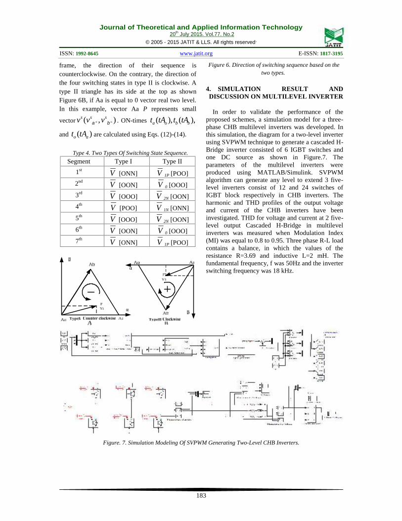
In order to validate the performance of theproposed schemes, a simulation model for a three-phase CHB multilevel inverters was developed. Inthis simulation, the diagram for a two-level inverterusing SVPWM technique to generate a cascaded H-Bridge inverter consisted of 6 IGBT switches andone DC source as shown in Figure.7. Theparameters of the multilevel inverters wereproduced using MATLAB/Simulink. SVPWMalgorithm can generate any level to extend 3 five-level inverters consist of 12 and 24 switches ofIGBT block respectively in CHB inverters. Theharmonic and THD profiles of the output voltageand current of the CHB inverters have beeninvestigated. THD for voltage and current at 2 five-level output Cascaded H-Bridge in multilevelinverters was measured when Modulation Index(MI) was equal to 0.8 to 0.95. Three phase R-L loadcontains a balance, in which the values of theresistance R=3.69 and inductive L=2 mH. Thefundamental frequency, f was 50Hz and the inverterswitching frequency was 18 kHz.
Figure. 7. Simulation Modeling Of SVPWM Generating Two-Level CHB Inverters.

Journal of Theoretical and Applied Information Technology20th July 2015. Vol.77. No.2
© 2005 - 2015 JATIT & LLS. All rights reserved.
ISSN: 1992-8645 www.jatit.org E-ISSN: 1817-3195
184
Figure. 8. Simulation Modeling SVPWM Generating Three Level CHB Inverters.
Figure. 9. Simulation Modeling SVPWM Generating Five Level CHB Inverters.

Journal of Theoretical and Applied Information Technology20th July 2015. Vol.77. No.2
© 2005 - 2015 JATIT & LLS. All rights reserved.
ISSN: 1992-8645 www.jatit.org E-ISSN: 1817-3195
185
4.1 Two-level cascaded H-Bridge inverter.
Line voltage and filtered voltage for the three-phase cascaded H-Bridge two-level inverter withmodulation index of 0.8-0.95 are shown in Figures8-9 and Figure 10, respectively. Meanwhile, currentmeasurement for the three-phase inverter is shownin Figure 11. FFT analysis of the two-levelcascaded H-bridge inverter with SVPWM is shownin Figures 12-13. For the two-level multilevelinverter, at MI=0.8, THD is equal to 36.61% ascompared to THD of 28.07% at MI=0.95. Figure 14shows that harmonic voltage filtered for two-levelinverter is equal to 3.44%. THD measurementcurrent is 3.94% as shown in Figure 15.
Figure 8. Line Voltage For Two-Level Inverter At
MI=0.8.
Figure 9. Line Voltage For Two-Level Inverter At
MI=0.95.
0 0.02 0.04 0.06 0.08 0.1 0.12 0.14 0.16 0.18 0.2
-200
-100
0
100
200
Time(S)
Fil
tered
Vo
lta
ges(V
)
Figure 10. Filtered Voltage For Two-Level Inverter.
0 0.02 0.04 0.06 0.08 0.1 0.12 0.14 0.16 0.18 0.2-400
-300
-200
-100
0
100
200
300
400
Time(S)
Cu
rren
t(A
)
Figure 11. Three-phase current for two-level inverter.
0 2 4 6 8 10 12 14 16 18 200
0.5
1
1.5
Harmonic order
Fundamental (50Hz) = 368.4 , THD= 36.61%
Mag
(%
of
Fun
dam
enta
l)
Figure 12. Harmonic Voltage For Two-LevelInverter At MI=0.8.
0 0.05 0.1 0.15 0.2 0.25 0.3 0.35 0.4-400
-200
0
200
400Selected signal: 20 cycles. FFT window (in red): 7 cycles
Time (s)
0 5 10 15 200
0.5
1
1.5
2
2.5
Harmonic order
Fundamental (50Hz) = 416.9 , THD= 28.07%
Mag (
% of
Fun
dame
ntal)
Figure 13. Harmonic Voltage For Two-LevelInverter At MI=0.95.
0 2 4 6 8 10 12 14 16 18 200
0.5
1
1.5
2
Harmonic order
Fundamental (50Hz) = 213.8 , THD= 3.44%
Mag
(% o
f Fun
dam
enta
l)
Figure 14. Harmonic Voltage Filtered For Two-Level Inverter.
0 0.05 0.1 0.15 0.2 0.25 0.3 0.35 0.4
-50
0
50
Selected signal: 20 cycles. FFT window (in red): 2 cycles
Time (s)
0 5 10 15 200
0.5
1
1.5
2
2.5
Harmonic order
Fundamental (50Hz) = 78.81 , THD= 3.94%
Mag
(% o
f Fun
dam
enta
l)
Figure 15. Harmonic Current For Two-Level Inverter.

Journal of Theoretical and Applied Information Technology20th July 2015. Vol.77. No.2
© 2005 - 2015 JATIT & LLS. All rights reserved.
ISSN: 1992-8645 www.jatit.org E-ISSN: 1817-3195
186
4.2 Three-level cascaded H-Bridge inverter
Line voltage and filtered voltage for the three-phase cascaded H-Bridge three-level inverter withmodulation index of 0.8-0.95 are shown in Figures16-17 and Figure 18, respectively. Meanwhile,current measurement for the three-level inverter isshown in Figure 19. FFT analysis of the three-levelcascaded H-bridge inverter with SVPWM is shownin Figures 20-21. For the three-level inverter, atMI=0.8, THD is equal to 31.08% as compared toTHD of 25.91% at MI=0.95. Figure 22 shows thatharmonic voltage filtered for the three-level inverteris equal to 1.73%. THD measurement current is1.61% as shown in Figure 23.
Figure 16. Line Voltage For Three-Level Inverter At MI=
0.8.
Figure 17. Line Voltage For Three-Level Inverter At
MI=0.95.
0 0.02 0.04 0.06 0.08 0.1 0.12 0.14 0.16 0.18 0.2-150
-100
-50
0
50
100
150
Time(S)
Fil
tere
d V
olt
ag
e(V
)
Figure 18. Filtered Voltage For Three-Level Inverter.
0 0.02 0.04 0.06 0.08 0.1 0.12 0.14 0.16 0.18 0.2-30
-20
-10
0
10
20
30
Time(S)
Cu
rren
t(A
)
Figure 19. Three-Phase Current For Three-Level Inverter.
0 0.05 0.1 0.15 0.2 0.25 0.3 0.35 0.4-200
0
200Selected signal: 20 cycles. FFT window (in red): 1 cycles
Time (s)
0 5 10 15 200
0.5
1
1.5
2
Harmonic order
Fundamental (50Hz) = 203.8 , THD= 31.08%
Mag
(% o
f Fun
dam
enta
l)
Figure 20. Harmonic Voltage For Three-Level Inverter
At MI=0.8.
0 0.05 0.1 0.15 0.2 0.25 0.3 0.35 0.4-200
0
200Selected signal: 20 cycles. FFT window (in red): 2 cycles
Time (s)
0 5 10 15 200
0.5
1
1.5
2
Harmonic order
Fundamental (50Hz) = 219 , THD= 25.91%
Mag
(% o
f Fun
dam
enta
l)
Figure 21. Harmonic Voltage For Three-Level
Inverter at MI=0.95.

Journal of Theoretical and Applied Information Technology20th July 2015. Vol.77. No.2
© 2005 - 2015 JATIT & LLS. All rights reserved.
ISSN: 1992-8645 www.jatit.org E-ISSN: 1817-3195
187
0 0.05 0.1 0.15 0.2 0.25 0.3 0.35 0.4
-100
0
100
Selected signal: 20 cycles. FFT window (in red): 2 cycles
Time (s)
0 5 10 15 200
0.2
0.4
0.6
0.8
1
1.2
Harmonic order
Fundamental (50Hz) = 126.5 , THD= 1.73%
Mag
(% o
f Fun
dam
enta
l)
Figure 22. Harmonic Voltage Filtered For Three-Level Inverter.
0 0.05 0.1 0.15 0.2 0.25 0.3 0.35 0.4
-20
0
20
Selected signal: 20 cycles. FFT window (in red): 2 cycles
Time (s)
0 5 10 15 200
0.1
0.2
0.3
0.4
0.5
0.6
0.7
Harmonic order
Fundamental (50Hz) = 33.22 , THD= 1.61%
Mag
(% o
f Fun
dam
enta
l)
Figure 23. Harmonic Current For Three-LevelInverter.
4.3 Five-level cascaded H-Bridge inverter
Line voltage and filtered voltage for the three-phase cascaded H-Bridge five-level inverter withmodulation index of 0.8-0.95 are shown in Figures24-25 and Figure 26, respectively. Meanwhile,current measurement for the five-level inverter isshown in Figure 27. FFT analysis of the five-levelcascaded H-bridge inverter with SVPWM is shownin Figures 28-29. For the five-level inverter, atMI=0.8, THD is equal to 24.72% as compared toTHD of 21.62% at MI=0.95. Figure 30 shows thatharmonic voltage filtered for the five-level inverteris equal to 0.83%. THD measurement current is1.15% as shown in Figure 31. Figure 32 presentsthe comparison of n-level inverters in terms of totalharmonic distortion.
Figure 24. Line To Line Five Level MI 0.8.
Figure 25. Line To Line Five Level MI 0.95.
0 0.02 0.04 0.06 0.08 0.1 0.12 0.14 0.16 0.18 0.2-200
-150
-100
-50
0
50
100
150
200
Time(S)
Fil
tere
d V
olt
ag
e(V
)
Figure 26. Filtered Voltage For Five-LevelInverter.
0 0.02 0.04 0.06 0.08 0.1 0.12 0.14 0.16 0.18 0.2-20
-15
-10
-5
0
5
10
15
20
Time(S)
Cu
rren
t(A
)
Figure 27. Three-Phase Current For Five-LevelInverter.

Journal of Theoretical and Applied Information Technology20th July 2015. Vol.77. No.2
© 2005 - 2015 JATIT & LLS. All rights reserved.
ISSN: 1992-8645 www.jatit.org E-ISSN: 1817-3195
188
0 0.005 0.01 0.015 0.02 0.025 0.03
-200
0
200
Selected signal: 1.713 cycles. FFT window (in red): 1 cycles
Time (s)
0 5 10 15 200
1
2
3
4
5
6
Harmonic order
Fundamental (50Hz) = 272.5 , THD= 24.72%M
ag (%
of F
unda
men
tal)
Figure 28. Harmonic Voltage For Five-LevelInverter At MI=0.8.
0 0.02 0.04 0.06 0.08 0.1
-200
0
200
Selected signal: 5 cycles. FFT window (in red): 1 cycles
Time (s)
0 5 10 15 200
2
4
6
8
Harmonic order
Fundamental (50Hz) = 351.3 , THD= 21.62%
Mag
(% o
f Fun
dam
enta
l)
Figure 29. Harmonic Voltage For Five-LevelInverter At MI=0.95.
0 0.05 0.1 0.15 0.2 0.25 0.3 0.35 0.4-200
0
200Selected signal: 20 cycles. FFT window (in red): 1 cycles
Time (s)
0 5 10 15 200
0.1
0.2
0.3
0.4
0.5
0.6
Harmonic order
Fundamental (50Hz) = 202 , THD= 0.83%
Mag
(% o
f Fun
dam
enta
l)
Figure 30. Harmonic Voltage Filtered For Five-Level Inverter.
0 0.01 0.02 0.03 0.04 0.05 0.06-200
0
200
Selected signal: 3.007 cycles. FFT window (in red): 2 cycles
Time (s)
0 5 10 15 200
0.1
0.2
0.3
0.4
0.5
0.6
Harmonic order
Fundamental (50Hz) = 252.1 , THD= 1.15%
Mag
(% o
f Fun
dam
enta
l)
Figure 31. Harmonic Current For Five-Level Inverter.
5. CONCLUSION
This paper presents harmonic comparativestudy of a three-phase (CHB) multilevel inverter byproposing a general SVPWM algorithm based onstandard 2 five-level SVPWM. Simulink modelswere developed for the space vector modulationCHB inverter. The proposed modulation wascompared to 2 three- and five-level cascadedinverters to reduce high total harmonic distortion,high switching losses and reduce cost based onCHB. From the study, better performance isobtained when the modulation index increases.

Journal of Theoretical and Applied Information Technology20th July 2015. Vol.77. No.2
© 2005 - 2015 JATIT & LLS. All rights reserved.
ISSN: 1992-8645 www.jatit.org E-ISSN: 1817-3195
189
36.61
28.07
3.94 3.44
31.0825.91
1.61 1.73
24.7221.62
1.150.83
0
10
20
30
40
THD%
Multilevel Inverters For THD
Two level Three Level Five Level
Figure 32. N-Level Inverter For Harmonic Reduction.
ACKNOWLEDGMENTS
The authors wish to thank Universiti TeknikalMalaysia Melaka (UTeM). This work wassupported primarily by the PJP Project codePJP/2012/UTEM-FKE/4 M00012.
REFRENCES:[1] M. S. Rosli Omar, Mohammed Rasheed,
“Fundamental Studies of a Three PhaseCascaded H-Bridge and Diode ClampedMultilevel Inverters Using Matlab/Simulink,”Int. Rev. Autom. Control, vol. 6, no. 5, 2013.
[2] R. Omar, M. Rasheed, and M. Sulaiman, “ASurvey of Multilevel Inverter based onCascaded H-Bridge Topology and ControlSchemes,” vol. 3, no. 2, pp. 1097–1108, 2015.
[3] R. Omar, M. Rasheed, A. Al-janad, M.Sulaiman, and Z. Ibrahim, “HARMONICREDUCTION COMPARISON INMULTILEVEL INVERTERS FORINDUSTRIAL APPLICATION,” vol. 63, no.3, pp. 570–578, 2014.
[4] A. K. Gupta, S. Member, A. M. Khambadkone,and S. Member, “A General Space VectorPWM Algorithm for Multilevel Inverters ,Including Operation in OvermodulationRange,” vol. 22, no. 2, pp. 517–526, 2007.
[5] P. Karuppanan and K. Mahapatra, “CascadedMultilevel Inverter based Active Filter forPower Line Conditioners using InstantaneousReal-Power Theory,” India Int. PowerElectron., vol. 769008, pp. 1–6, 2011.
[6] X. Yang, C. Wang, L. Shi, and Z. Xia,“Generalized Space Vector Pulse WidthModulation Technique for Cascaded Multilevel
Inverters,” Int. J. Control Autom., vol. 7, no. 1,pp. 11–26, Jan. 2014.
[7] M. Tan, “A two-level,” no. 1, pp. 1823–1828,2004.
[8] A. K. Gupta, S. Member, A. M. Khambadkone,and S. Member, “A Space Vector PWMScheme for Multilevel Inverters Based onTwo-Level Space Vector PWM,” vol. 53, no.5, pp. 1631–1639, 2006.
[9] A. K. Gupta and A. M. Khambadkone, “ASimple Space Vector PWM Scheme to Operatea Three-Level NPC Inverter at HighModulation Index Including OvermodulationRegion, With Neutral Point Balancing,” IEEETrans. Ind. Appl., vol. 43, no. 3, pp. 751–760,2007.
[10] L. Saribulut, A. Teke, and M. Tümay, “Vector-based reference location estimating for spacevector modulation technique,” Electr. PowerSyst. Res., vol. 86, pp. 51–60, May 2012.
[11] M. Valan Rajkumar and P. S. Manoharan,“FPGA based multilevel cascaded inverterswith SVPWM algorithm for photovoltaicsystem,” Sol. Energy, vol. 87, pp. 229–245,Jan. 2013.
[12] S. Wei and B. Wu, “A general space vectorPWM control algorithm for multilevelinverters,” Eighteenth Annu. IEEE Appl. PowerElectron. Conf. Expo. 2003. APEC ’03., vol. 1,no. 1, pp. 562–568, 2003.