Embed Size (px)
Citation preview
Supporting Information
“Effect of Pre-aggregation on Directional Alignment
of Conjugated Polymer for High Performance
Organic Field Effect Transistors”
Nam-Koo Kim,† Soo-Young Jang,
† Giuseppina Pace,
∥ Mario Caironi,
∥ Won-
Tae Park§, Dongyoon Khim
§, Juhwan Kim,
# Dong-Yu Kim*
†, and Yong-Young
Noh*§
†Department of Nanobio Materials and Electronics, School of Material Science and
Engineering, Heeger Center for Advanced Materials, Gwangju Institute of Science and
Technology (GIST), 261 Cheomdan-gwagiro (Oryong-dong), Buk-gu, Gwangju 500-712,
Republic of Korea
§Department of Energy and Materials Engineering, Dongguk University, 26 Pil-dong, 3-ga,
Jung-gu, Seoul 100-715, Republic of Korea,
∥Center for Nano Science and Technology @PoliMi, Istituto Italiano di Tecnologia, Via
Pascoli 70/3, 20133 Milano, Italy,
#Department of Chemical Engineering and Material Science, University of California, Irvine,
California 92697, United States
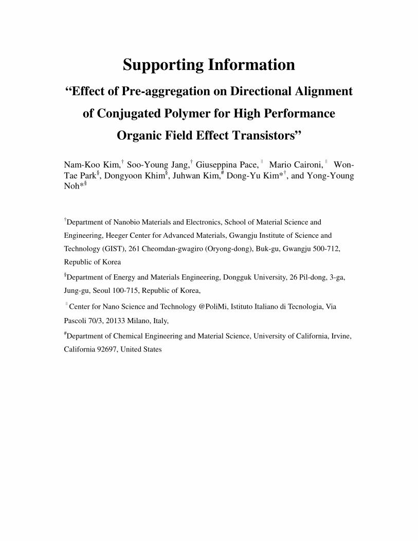
S1. Gran size analysis mode of Atomic Force Microscopy (AFM)
Figure S1. AFM phase image in grain size analysis mode of (a) P3HT, (b) DPPT-TT, (c) P-
18, (d) P(NDI2OD-T2) (CB) (e) P(NDI2OD-T2) (Tol).
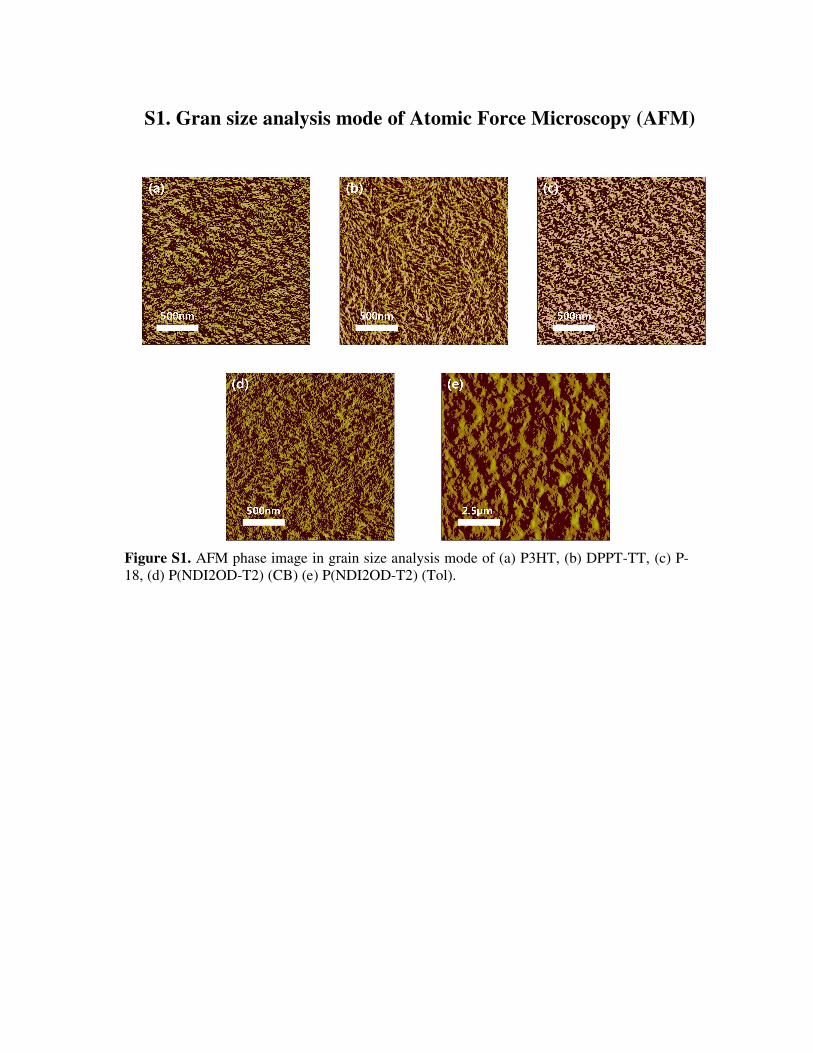
S2. Anisotropic dependence of charge transport properties
Figure S2. (a) Field effect mobility of orthogonal and parallel devices and standard deviation
depending on distance from spinning center using DPPT-TT semiconductor and (b) average
field effect mobility of each orthogonal and parallel devices at the saturation region.
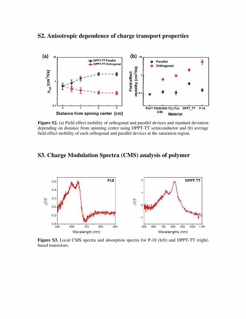
S3. Charge Modulation Spectra (CMS) analysis of polymer
Figure S3. Local CMS spectra and absorption spectra for P-18 (left) and DPPT-TT (right)
based transistors.
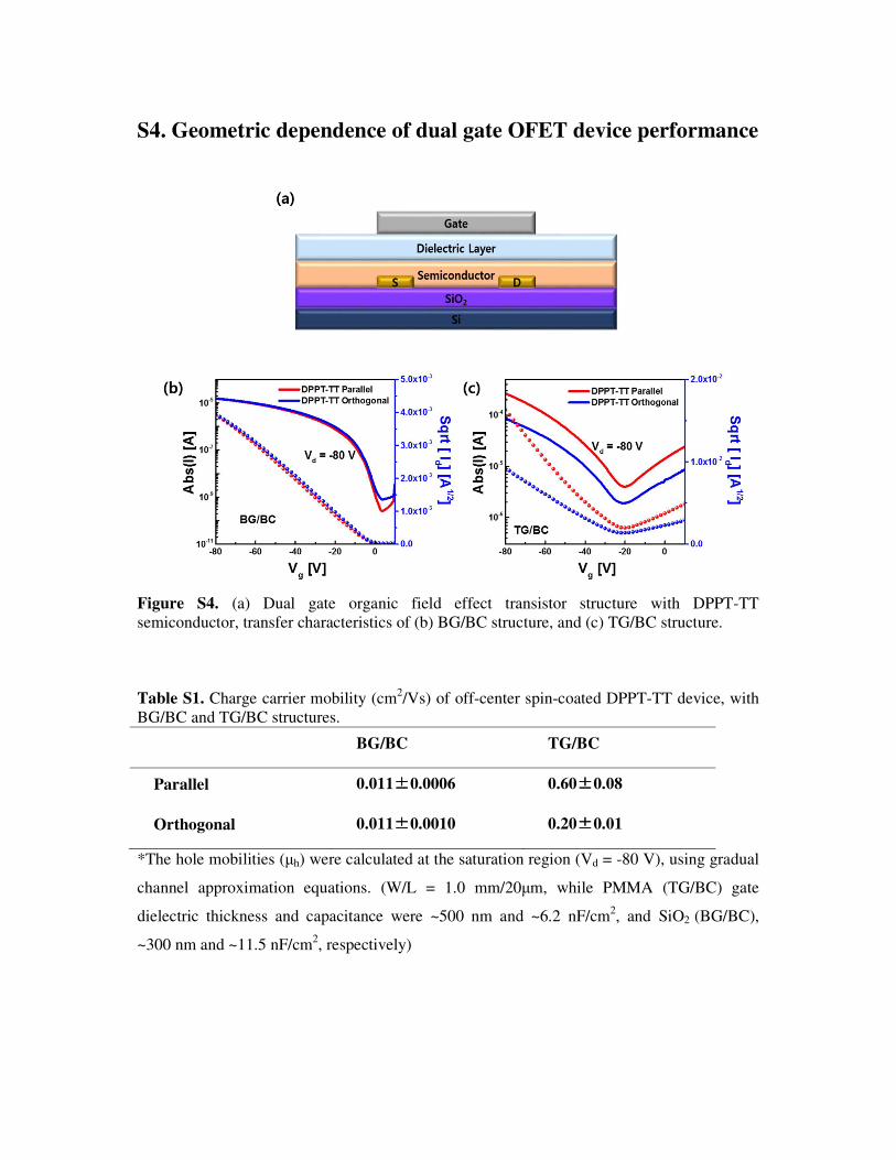
S4. Geometric dependence of dual gate OFET device performance
Figure S4. (a) Dual gate organic field effect transistor structure with DPPT-TT
semiconductor, transfer characteristics of (b) BG/BC structure, and (c) TG/BC structure.
Table S1. Charge carrier mobility (cm2/Vs) of off-center spin-coated DPPT-TT device, with
BG/BC and TG/BC structures.
BG/BC TG/BC
Parallel 0.011±±±±0.0006 0.60±±±±0.08
Orthogonal 0.011±±±±0.0010 0.20±±±±0.01
*The hole mobilities (µh) were calculated at the saturation region (Vd = -80 V), using gradual
channel approximation equations. (W/L = 1.0 mm/20µm, while PMMA (TG/BC) gate
dielectric thickness and capacitance were ~500 nm and ~6.2 nF/cm2, and SiO2 (BG/BC),
~300 nm and ~11.5 nF/cm2, respectively)
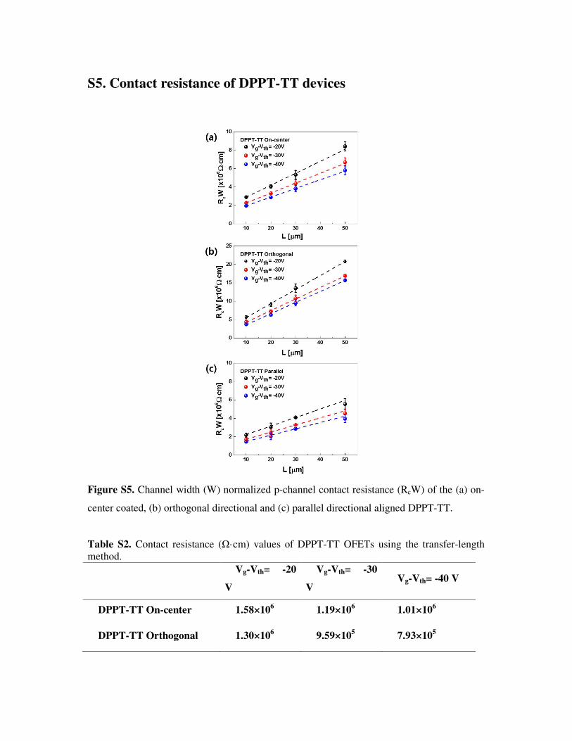
S5. Contact resistance of DPPT-TT devices
Figure S5. Channel width (W) normalized p-channel contact resistance (RcW) of the (a) on-
center coated, (b) orthogonal directional and (c) parallel directional aligned DPPT-TT.
Table S2. Contact resistance (Ω·cm) values of DPPT-TT OFETs using the transfer-length
method.
Vg-Vth= -20
V
Vg-Vth= -30
V Vg-Vth= -40 V
DPPT-TT On-center 1.58×10⁶ 1.19×10
6 1.01×10
6
DPPT-TT Orthogonal 1.30×10⁶ 9.59×10
5 7.93×10
5
DPPT-TT Parallel 1.75×10⁶ 1.18×10
6 5.95×10
5
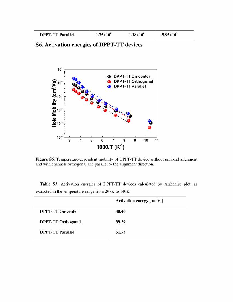
S6. Activation energies of DPPT-TT devices
Figure S6. Temperature-dependent mobility of DPPT-TT device without uniaxial alignment
and with channels orthogonal and parallel to the alignment direction.
Table S3. Activation energies of DPPT-TT devices calculated by Arrhenius plot, as
extracted in the temperature range from 297K to 140K.
Activation energy [ meV ]
DPPT-TT On-center 40.40
DPPT-TT Orthogonal 39.29
DPPT-TT Parallel 51.53