Embed Size (px)
Citation preview

A U G U S T 1 9 8 1
> %
K-; C? 'Ã:
.
r ' :
vm
R E G U U A . T E D D C
C O N T R O L
© Copr. 1949-1998 Hewlett-Packard Co.
H E W L E T T - P A C K A R D J O U R N A L Technica l In format ion f rom the Laborator ies of Hewlet t -Packard Company
C o n t e n t s : A U G U S T 1 9 8 1 V o l u m e 3 2 â € ¢ N u m b e r 8
2 0 0 - k H z P o w e r F E T T e c h n o l o g y i n N e w M o d u l a r P o w e r S u p p l i e s , b y R i c h a r d M y e r s and Rober t D. Peck These 50 W pr in ted-c i rcu i t board suppl ies are h igh ly re l iab le and meet
wor ldwide safe ty s tandards.
M a g n e t i c C o m p o n e n t s f o r H i g h - F r e q u e n c y S w i t c h i n g P o w e r S u p p l i e s , b y W i n f r i e d Se ipe l manu goa ls were sma l l s i ze , 200-kHz opera t ion , sa fe ty , and semiau tomated manu
facturing.
L a b o r a t o r y - P e r f o r m a n c e A u t o r a n g i n g P o w e r S u p p l i e s U s i n g P o w e r M O S F E T T e c h no logy , by Denn is W. Gyma, Pau l W. Ba i ley , John W. Hyde, and Dan ie l P . Schwar tz These
are prec is ion 200W and 1000W suppl ies des igned for a var ie ty o f laboratory , indust r ia l , and sys tems appl icat ions.
The Ver t i ca l Power MOSFET fo r H igh -Speed Power Con t ro l , by Kar l H . T ie fe r t , Dah Wen Tsang , powe r L Mye rs , and V i c t o r L i W i t h cu r ren t f l ow ing ve r t i ca l l y , mo re powe r can be
swi tched wi thout sacr i f i c ing swi tch ing speed.
P o w e r L i n e D i s t u r b a n c e s a n d T h e i r E f f e c t o n C o m p u t e r D e s i g n a n d P e r f o r m a n c e , b y Ar thur o f Due l l and W. V incent Ro land Proper s i te w i r ing , adequate g round ing , and use o f
iso la t ion dev ices he lp assure sat is factory per formance.
In this Issue: When we that someth ing in to an e lec t r ica l out le t we are connect ing i t to a vo l tage that
alternates between posit ive and negative values 50 or 60 times per second, depending on the country. This vol tage may be subject to random noise and to large, unpredictable, sudden f luc tuat ions as the u t i l i t y company supp ly ing us wi th e lec t r ic power exper iences demand variat ions, electr ical storms, equipment problems, and other disturbances. Electronic circuits l ike and in television sets, computers, stereo systems, and electronic instruments don't l ike th is k ind o f power . They need s teady , we l l regu la ted , ba t te ry - l i ke vo l tages . Large d is tu r bances can d isrupt or even dest roy them.
The ar t ic les in th is issue deal wi th the problems of changing unregulated al ternat ing vol tages to regulated battery-l ike ones, and of dealing with unpredictable power anomalies. The f irst two art icles are about the design of some innovative new power supplies. Power supplies are electronic devices that convert what comes out of an electr ical out let to regulated voltages for other electronic devices to use. For example, there's a power supply inside small piece of electronic equipment. This kind of power supply should be small and as reliable as the wall outlet page plugged into. The 65000A Series Modular Power Supplies (cover and page 3) are of this type. There are also cabinets. supplies that provide regulated voltages to circuits outside their own cabinets. These might be found computer-controlled on a lab engineer's bench or mounted in a rack as part of a computer-controlled test system. These supplies programmable. be extremely well regulated, accurate, and for some applications remotely programmable. Models category. and 6024A Autoranging Power Suppl ies (page 11) are in this category.
Al though of are meant for d i f ferent appl icat ions and represent d i f ferent design approaches, both of these new power supply fami l ies take advantage of a new HP swi tching t ransistor cal led a power MOSFET (metal - oxide-semiconductor f ield-effect transistor). MOSFETs have been around for a whi le and their superior i ty over o ther we l l o f t rans is tors fo r many h igh- f requency app l ica t ions is we l l known. However , unt i l recent ly there weren't any with the HP device's combination of high voltage rat ing, fast switching speed, low resistance, high rel iabi l i ty, and small chip size. The cover photograph shows where the HP power MOSFET f i ts in the schematic diagram different a 65000A Power Supply. On page 18 is an article about the new MOSFET, telling why it's different and how i t 's made.
The spec ia l p rob lems power l i ne d i s tu rbances cause compute rs ( i n sp i te o f t he i r we l l regu la ted power supplies) conditions, discussed in the article on page 25. This article is based on studies of typical power line conditions, wir ing codes for bui ld ings, computer insta l la t ion procedures, and computer designs. The ar t ic le should be of in terest to anyone who owns a computer system or is cons ider ing insta l l ing one.
-R. P. Do/an
Editor, Richard P. Dolan • Associate Editor, Kenneth A. Shaw • Art Director, Photographer, An/id A. Danielson I l lustrator, Nancy S. Vanderbloom • Administrat ive Services, Typography, Anne S. LoPrest i • European Product ion Manager, Dick Leeksma
2 H E W L E T T - P A C K A R D J O U R N A L A U G U S T 1 9 8 1 Â © H e w l e t t - P a c k a r d C o m p a n y 1 9 8 1 P r i n t e d i n U . S . A .
© Copr. 1949-1998 Hewlett-Packard Co.
200-kHz Power FET Technology in New Modular Power Suppl ies These smal l , re l iab le 50-wat t suppl ies are des igned for OEM (or ig ina l equ ipment manufacturer ) use anywhere in the world.
by Richard Myers and Robert D. Peck
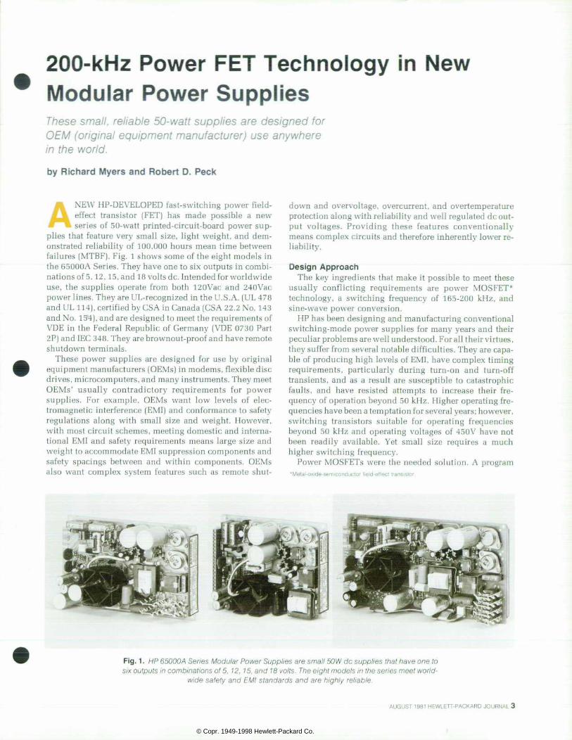
ANEW HP-DEVELOPED fast-switching power field- effect transistor (FET) has made possible a new series of 50-watt printed-circuit-board power sup
plies that feature very small size, light weight, and dem onstrated reliability of 100,000 hours mean time between failures (MTBF). Fig. 1 shows some of the eight models in the 65000A Series. They have one to six outputs in combi nations of 5, 12, 15, and 18 volts dc. Intended for worldwide use, the supplies operate from both 120Vac and 240Vac power lines. They are UL-recognized in the U.S.A. (UL 478 and UL 114), certified by CSA in Canada (CSA 22.2 No. 143 and No. 15*4), and are designed to meet the requirements of VDE in the Federal Republic of Germany (VDE 0730 Part 2P) and IEC 348. They are brownout-proof and have remote shutdown terminals.
These power supplies are designed for use by original equipment manufacturers (OEMs) in modems, flexible disc drives, microcomputers, and many instruments. They meet OEMs' usually contradictory requirements for power supplies. For example, OEMs want low levels of elec tromagnetic interference (EMI) and conformance to safety regulations along with small size and weight. However, with most circuit schemes, meeting domestic and interna tional EMI and safety requirements means large size and weight to accommodate EMI suppression components and safety spacings between and within components. OEMs also want complex system features such as remote shut
down and overvoltage, overcurrent, and overtemperature protection along with reliability and well regulated dc out put voltages. Providing these features conventionally means complex circuits and therefore inherently lower re liability.
Design Approach The key ingredients that make it possible to meet these
usually conflicting requirements are power MOSFET technology, a switching frequency of 165-200 kHz, and sine-wave power conversion.
HP has been designing and manufacturing conventional switching-mode power supplies for many years and their peculiar problems are well understood. For all their virtues , they suffer from several notable difficulties. They are capa ble of producing high levels of EMI, have complex timing requirements, particularly during turn-on and turn-off transients, and as a result are susceptible to catastrophic faults, and have resisted attempts to increase their fre quency of operation beyond 50 kHz. Higher operating fre quencies have been a temptation for several years; however, switching transistors suitable for operating frequencies beyond 50 kHz and operating voltages of 450V have not been readily available. Yet small size requires a much higher switching frequency.
Power MOSFETs were the needed solution. A program *Metal-oxide-semiconductor f ie ld-ef fect t ransistor .
Fig. supplies . to 65000A Series Modular Power Supplies are small SOW dc supplies that have one to six outputs in combinat ions of 5, 12, 15, and 18 vol ts. Theeight models in the ser ies meet world
wide safety and EMI s tandards and are h igh ly re l iab le .
AUGUST 1981 HEWLETT-PACKARD JOURNAL 3
© Copr. 1949-1998 Hewlett-Packard Co.
was begun at HP to develop power FETs with characteris tics suitable for off-line switching regulators (see article, page 18). However, it then became apparent that power switches were only part of the high-frequency problems. The construction of transformers that simultaneously meet worldwide safety requirements and have leakage induc tance commensurate with standard pulse-width modula tion techniques is no small matter. High-frequency opera tion of transformers in a conventional pulse- width modula tion mode is difficult to achieve. If a transformer is designed to be thermally limited (fixed temperature rise) and its frequency of operation is increased, the per-unit leakage inductance of the transformer increases approximately as the square root of the frequency. Leakage inductance results in power dissipation in snubber circuits, EMI, increased open-loop output impedance, and increased stress on power semiconductors. Clearly, if high-frequency opera tion is desired some method of eliminating the undesirable effects of leakage inductance had to be found.
Sine-Wave Vol tage Regula t ion The power conversion and voltage regulation technique
used in the 65000A Series eliminates many of the bad ef fects of leakage inductance. 165-to-200-kHz square waves are converted to sine waves as an integral part of the regula tion process. This voltage regulation technique can be explained with the circuit shown in Fig. 2. The circuit is a simple series resonant tank, and the voltage source Eg is a square-wave generator. The low-pass characteristic of the tank circuit effectively filters the square wave and converts it to a sine wave.
For the purpose of analysis consider the source to be a sinusoidal source whose output is equal to the magnitude of the fundamental component of the square wave. This ap proximation allows routine ac analysis to be used and simplifies the mathematics considerably. RL represents the load connected to the output of the power supply, plus rectifier, switch, and magnetic losses. L and C are the energy storage elements of the resonant tank.
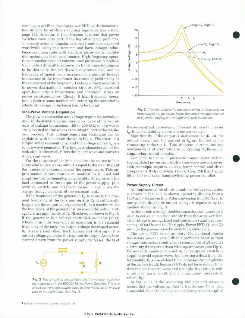
If the frequency of the generator, fg, is equal to the reso nant frequency of the tank and resistor RL is sufficiently large, then the output voltage across RL is a maximum. As the frequency of the generator is increased the output volt age falls asymptotically at 12 dB/octave, as shown in Fig. 3. If the generator is a voltage-controlled oscillator (VCO) whose minimum frequency of operation is the resonant frequency of the tank, the output voltage developed across RL is easily controlled. Rectification and filtering of this output voltage generates the required dc output. As the load current drawn from the power supply decreases, the Q of
H i g h E g , H i g h R L
L o w E 9 , H i g h R L
- 2 0
Fig. 2 This s impl i f ied c i rcui t i l lustrates the vol tage regulat ion technique used in the 65000 A Series Power Supplies . The tank c i rcui t converts the square wave to s ine waves as an integral par t o f the techn ique. See F ig . 3 .
Frequency
Fig. the Transfer function for the circuit of Fig. 2. Adjusting the f requency of the generator keeps the output vol tage constant at V0 under vary ing l ine vol tage and load condi t ions.
the resonant tank increases and the control circuit increases fg, thus maintaining a constant output voltage.
Significantly, if the output is short-circuited (RL=O) the output current and the current in Eg are limited by the resonating inductor L. This inherent current-limiting mechanism is of great value in controlling faults and in simplifying control circuits.
Compared to the usual pulse-width-modulation switch ing regulated power supply, this sine- wave power conver sion technique requires 25-33% fewer control and drive components. It also provides 1 5-20 dB less EMI than typical 50-to-100-watt open-frame switching power supplies.
Power Supply Circuit An implementation of this circuit for voltage regulation
is shown in Fig. 4. It is shown operating directly from a 120Vac 60-Hz power line. After conversion from 60-Hz ac to unregulated dc, the dc output voltage is regulated by the method shown in Fig. 3.
In this circuit a bridge-doubler capacitor configuration is used to derive a ±160Vdc supply from the ac power line. This voltage is unregulated and contains a significant per centage of 60-Hz and 1 20-Hz ripple. Power FETs Ql and Q2 provide the square wave by switching alternately.
The use of FETs is not arbitrary. Conventional bipolar transistors present very difficult problems because their storage time makes simultaneous conduction of Ql and Q2 a certainty if they are driven with square waves (see Fig. 4). Pulse-width modulators used in conventional switching supplies avoid square waves by inserting a dead time. Un fortunately, this use of dead time increases the complexity of the driver circuit. Because FETs do not have storage time, they can use a square wave and a simple drive circuit, with a reduced parts count and a consequent increase in reliability.
In Fig. 4, Ll is the resonating inductor and serves to insure that the voltage applied to transformer Tl is truly sinusoidal. Since the voltage rate of change (dv/dt) applied
4 H E W L E T T - P A C K A R D J O U R N A L A U G U S T 1 9 8 1
© Copr. 1949-1998 Hewlett-Packard Co.

r H ,
rB l·^ r : V R E F
Ã̄ to the transformer is significantly reduced by Ll, the prob lem of EMI is dramatically lessened. Q,^^ serves to insure that no dc current is allowed to circulate in Tl. CR, the resonating capacitor, appears on the secondary of trans former Tl. Notice that this placement of CR effectively puts the leakage inductance of transformer Tl in series with resonating inductor Ll. A price is paid, however, for this tuning out of the leakage inductance. The rms current in the resonating capacitor is nearly the same as the dc output current. This made it necessary to develop high-current capacitors for the 65000A Series, as discussed later in this article.
Rectifiers Dl and D2 and the output filter (Lf and Cf) constitute a conventional center-tapped full-wave rectifier and averaging filter. Significantly, the required inductor Lf is smaller than an equivalent filter inductor in a pulse- width modulator by a factor of nearly 2.5 to 1. This reduc tion is possible because sine waves are being filtered in stead of a pulse train.
The filtered output voltage Vdc is compared to the desired output voltage VREF, amplified and applied to a voltage- controlled oscillator. The oscillator is used to drive the power FETs and regulate the output voltage. A special magnetic component developed for the oscillator allows the frequency of a square-wave oscillator to be controlled by varying the current in a winding. This control inductor was selected because of its simplicity, reliability, and ability to meet worldwide safety standards.
Several characteristics of this power supply circuit make it especially attractive for use in the 65000A Series. It uses a simple and reliable control technique with standard linear circuits and without recourse to complex and unwieldly pulse-width circuits. It has inherent current limiting that requires no additional circuitry. A short on the output rec tifiers, resonating capacitors, or transformer will actually produce a decrease in the FET current.
High-frequency operation can be easily achieved. The 65000A Series operates at frequencies in excess of 200 kHz and is designed to meet worldwide safety specifications. The output choke in the output averaging filter is 2.5 times smaller than an equivalent choke in a pulse-width mod ulated unit. EMI problems are minimized because of the presence of sinusoidal waveforms at all points beyond the resonating inductor Ll. The simple control techniques re sult in a lower parts count and a much improved MTBF
Fig . 4 . S imp l i f i ed schemat ic o f a 6 5 0 0 0 A - t y p e o f f - l i n e s i n e - w a v e converter.
(greater than 100,000 hours MTBF demonstrated for a single-output unit with 395,000 unit hours of life tests).
The disadvantage of the circuit is that it requires an extra magnetic component (resonating inductor Ll) and a resonating capacitor CR. However, this disadvantage is more than compensated by the sharp reduction in size re sulting from the increased frequency of operation (al most 10:1).
Voltage-Control led Osci l lator The novel voltage-controlled oscillator provides more
than one ampere of drive current to the FETs using only eight components. It is an inductively coupled, astable mul tivibrator. A simplified circuit diagram is shown in Fig. 5.
To understand the oscillator's operation assume that transistor Q4 is conducting. The current ITS is equal to (KVCC - VBE)/RS and is constant. Because VBE is positive, transistor Q5 is held off and voltage Vcc is applied to the primary of transformer Tl . The voltage VL(t) is positive and results in an increasing current iL(t) and eventually ITS =
m 2 V C C
I B 4
Power FETs
Fig. pro High-current vol tage-contro l led osci l la tor (VCO) pro v ides more than one ampere to d r i ve the power MOSFETs , using only eight components. L is a var iable control inductor; t he osc i l l a to r f r equency i s con t ro l l ed by va ry ing t he i nduc tance of L.
AUGUST 1981 HEWLETT-PACKARD JOURNALS
© Copr. 1949-1998 Hewlett-Packard Co.
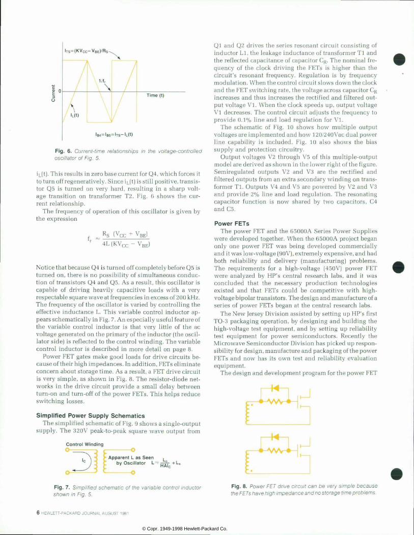
|TS=(KVCC-VBE)/RS
iB4=iB5=iTS-iL(t)
F ig . 6 . Cur ren t - t ime re la t ionsh ips in the vo l tage-con t ro l l ed osci l lator of Fig. 5.
ÃL(Ã). This results in zero base current for Q4, which forces it to turn off regeneratively. Since ÃL(I) is still positive, transis tor Q5 is turned on very hard, resulting in a sharp volt age transition on transformer T2. Fig. 6 shows the cur rent relationship.
The frequency of operation of this oscillator is given by the expression
R + VBE)
4L (KVCC - VBE)
Notice that because Q4 is turned off completely before Q5 is turned on, there is no possibility of simultaneous conduc tion of transistors Q4 and Q5. As a result, this oscillator is capable of driving heavily capacitive loads with a very respectable square wave at frequencies in excess of 200 kHz. The frequency of the oscillator is varied by controlling the effective inductance L. This variable control inductor ap pears of in Fig. 7. An especially useful feature of the variable control inductor is that very little of the ac voltage generated on the primary of the inductor (the oscil lator side) is reflected to the control winding. The variable control inductor is described in more detail on page 8.
Power FET gates make good loads for drive circuits be cause of their high impedances. In addition, FETs eliminate concern about storage time. As a result, a FET drive circuit is very simple, as shown in Fig. 8. The resistor-diode net works in the drive circuit provide a small delay between turn-on and turn-off of the power FETs. This helps reduce switching losses.
Simpl i f ied Power Supply Schemat ics The simplified schematic of Fig. 9 shows a single-output
supply. The 320V peak-to-peak square wave output from
Control Winding O -
Apparent L as Seen b y O s c i l l a t o r L =
Ql and Q2 drives the series resonant circuit consisting of inductor LI, the leakage inductance of transformer Tl and the reflected capacitance of capacitor CR. The nominal fre quency of the clock driving the FETs is higher than the circuit's resonant frequency. Regulation is by frequency modulation. When the control circuit slows down the clock and the FET switching rate, the voltage across capacitor CR increases and thus increases the rectified and filtered out put voltage VI. When the clock speeds up, output voltage VI decreases. The control circuit adjusts the frequency to provide 0.1% line and load regulation for VI.
The schematic of Fig. 10 shows how multiple output voltages are implemented and how 120/240 Vac dual power line capability is included. Fig. 10 also shows the bias supply and protection circuitry.
Output voltages V2 through V5 of this multiple-output model are derived as shown in the lower right of the figure. Semiregulated outputs V2 and V3 are the rectified and filtered outputs from an extra secondary winding on trans former Tl. Outputs V4 and V5 are powered by V2 and V3 and provide 2% line and load regulation. The resonating capacitor function is now shared by two capacitors, C4 and C5.
Power FETs The power FET and the 65000A Series Power Supplies
were developed together. When the 65000A project began only one power FET was being developed commercially and it was low-voltage (90V), extremely expensive, and had both reliability and delivery (manufacturing) problems. The requirements for a high-voltage (450V) power FET were analyzed by HP's central research labs, and it was concluded that the necessary production technologies existed and that FETs could be competitive with high- voltage bipolar transistors. The design and manufacture of a series of power FETs began at the central research labs.
The New Jersey Division assisted by setting up HP's first TO-3 packaging operation, by designing and building the high-voltage test equipment, and by setting up reliability test equipment for power semiconductors. Recently the Microwave Semiconductor Division has picked up respon sibility for design, manufacture and packaging of the power FETs and now has its own test and reliability evaluation equipment.
The design and development program for the power FET
M- J
J
Fig . 7 . S impl i f ied schemat ic o f the var iab le cont ro l inductor shown in Fig. 5.
F ig . 8 . Power FET dr ive c i rcu i t can be very s imple because the FETs have high impedance and no storage t ime problems.
6 HEWLETT-PACKARD JOURNAL AUGUST 1981
© Copr. 1949-1998 Hewlett-Packard Co.

Input Rectifier
Ser ies Resonant T a n k a n d S c h o t t k y
T r a n s f o r m e r R e c t i f i e r Four-Pole
Output Filter
AC
Fig. Power Supply. schemat ic of a s ingle-output 65000A Ser ies Power Supply.
was different from a development program for a typical high-voltage power transistor. The performance of a FET can be accurately predicted and so the extensive ex perimentation and redesign that characterize bipolar de velopment programs were not necessary. Along with pre dictable performance, manufactured FETs have consistent gains and switching speeds. Consistency and predictability are major advantages of FETs over bipolar power transistors and were crucial in the decision to develop a power FET just for switching power supplies.
While the electrical performance was predictable, the challenge for the research labs was to develop HP's first- high-voltage manufacturing process and make reliable FETs. A high voltage rating of 450 volts is necessary for any off-line power supply designed to operate from 240Vac as used in Europe. A high voltage rating requires high- resistivity silicon, which leads to high on resistance. Since high on resistance is undesirable, the FET production pro cess has to be precisely controlled so that every FET has a voltage capability that is high enough, but not too high — 470 to 530 volts is the permitted range. Another problem is that high voltages cause strong fields inside the FETs. These fields move any mobile ions present and thus change the threshold voltage and increase the drain leakage cur rent, possibly causing power supply failures. Mobile ions can result from contamination, so the FET manufacturing process must be very clean to reduce their number.
From the beginning of the project reliability was a major concern. A reliability demonstration of 500,000 hours was required before the FETs would be used in the 65000A Series Power Supplies. The time required for the demon stration was compressed by a factor of about 25 by testing at 175T! instead of the 125°C maximum temperature rating. After considerable effort by the research labs, the FETs passed the 1000-hour test with just two failures in 140
devices. With each process change by any vendor these tests are repeated. Samples are taken from lots and given similar reliability tests. In this way continuing reliability is assured.
The power FETs have met the original goals. They have the required voltage, low on resistance, fast and consistent switching speeds, consistent gains, good manufacturing yields, and reliability. This contrasts with and is a welcome improvement over the performance of high- voltage bipolar transistors.
Film Capacitors The resonant circuit regulation scheme of the 65000A
Series calls for a high-current film capacitor. The current in the capacitor is about 90% of the output current. This capacitor, required on the secondary of transformer TI (CR in Fig. 4), is physically large. Its operating current ap proaches the wire lead current rating and exceeds most manufacturers' current ratings for the capacitor winding end connections.
There were no commercially available capacitors with sufficient current ratings. Because the capacitor in the reso nant circuit has sinusoidal voltage and current waveforms, it was reasonable to expect that conventional low-cost film capacitors would be reliable. HP provided capacitor man ufacturers with test circuits to demonstrate successful sine-wave operation at high currents. Life tests were begun at HP to explore the possibility that new and unexpected failure mechanisms could be introduced by the high cur rents. These tests demonstrated that temperature was the prime concern and reliability required just careful thermal design. The capacitor type finally approved uses film-foil construction and polypropylene dielectric. Low-loss poly propylene capacitors and solid copper leads soldered di rectly to the foil in the capacitors met the reliability re-
(con t inued on page 10)
AUGUST 1981 HEWLETT-PACKARD JOURNAL?
© Copr. 1949-1998 Hewlett-Packard Co.
Magnetic Components for High-Frequency Switching Power Supplies
by Winfr ied Seipel
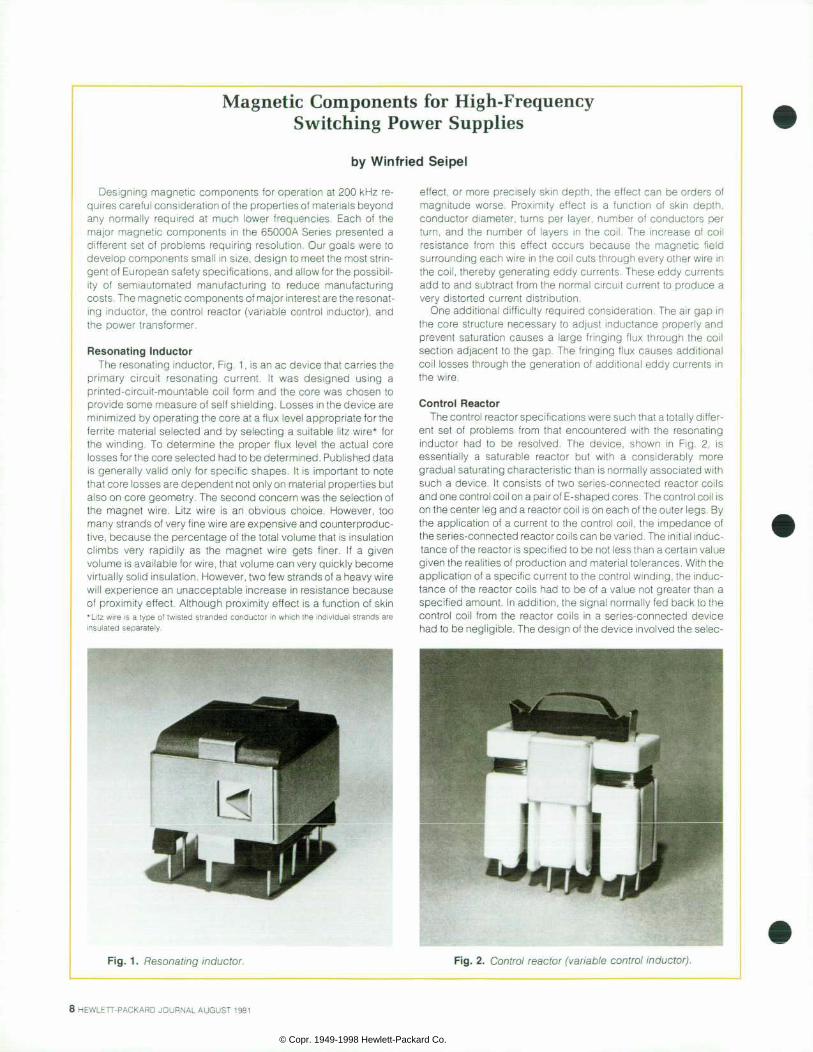
Des ign ing magnet i c components fo r opera t ion a t 200 kHz re quires careful considerat ion of the propert ies of materials beyond any no rma l l y requ i red a t much lower f requenc ies . Each o f t he ma jo r magne t i c componen ts in the 65000A Ser ies p resen ted a d i f ferent set o f problems requi r ing resolut ion. Our goals were to develop components smal l in s ize, design to meet the most s t r in gent of European safety speci f icat ions, and al low for the possibi l i t y o f sem iau toma ted manu fac tu r i ng t o r educe manu fac tu r i ng costs. The magnetic components of major interest are the resonat ing inductor , the cont ro l reactor (var iab le cont ro l inductor ) , and the power t ransformer .
Resonat ing Inductor The resonating inductor, Fig. 1 , is an ac device that carr ies the
p r i m a r y c i r c u i t r e s o n a t i n g c u r r e n t . I t w a s d e s i g n e d u s i n g a pr in ted-c i rcu i t -mountab le co i l fo rm and the core was chosen to provide some measure of sel f shielding. Losses in the device are minimized by operat ing the core at a f lux level appropriate for the ferr i te mater ia l se lected and by select ing a sui table l i tz wi re* for the w ind ing . To de te rmine the p roper f l ux leve l the ac tua l co re losses for the core selected had to be determined. Publ ished data is general ly val id only for speci f ic shapes. I t is important to note that core losses are dependent not only on material propert ies but a lso on core geometry. The second concern was the select ion of t he magne t w i re . L i t z w i re i s an obv ious cho i ce . However , t oo many st rands of very f ine wire are expensive and counterproduc t ive, because the percentage of the total volume that is insulat ion c l i m b s v e r y r a p i d i l y a s t h e m a g n e t w i r e g e t s f i n e r . I f a g i v e n volume is avai lable for wire, that volume can very quickly become virtually solid insulation. However, two few strands of a heavy wire wi l l exper ience an unacceptable increase in res is tance because of proximi ty ef fect . Al though proximi ty ef fect is a funct ion of sk in *L i tz w i re is a type o f tw is ted s t randed conductor in wh ich the ind iv idua l s t rands are insulated separate ly .
ef fect , or more prec ise ly sk in depth, the ef fect can be orders of magn i tude worse . P rox im i t y e f fec t i s a func t ion o f sk in dep th , conduc to r d iameter , tu rns per layer , number o f conduc to rs per tu rn , and the number o f layers in the co i l . The inc rease o f co i l r es i s tance f rom th i s e f fec t occu rs because the magne t i c f i e ld surrounding each wire in the coi l cuts through every other wire in the coi l , thereby generat ing eddy currents. These eddy currents add to a sub t rac t f rom the no rma l c i r cu i t cu r ren t to p roduce a very distor ted current d istr ibut ion.
One addi t ional di f f icul ty required considerat ion. The air gap in the core s t ruc ture necessary to ad jus t inductance proper ly and prevent sa tura t ion causes a la rge f r ing ing f lux through the co i l sect ion ad jacent to the gap. The f r ing ing f lux causes addi t ional c o i l i n t h r o u g h t h e g e n e r a t i o n o f a d d i t i o n a l e d d y c u r r e n t s i n the wire.
Control Reactor The control reactor specif icat ions were such that a total ly dif fer
en t se t o f p rob lems f rom tha t encounte red w i th the resonat ing i n d u c t o r h a d t o b e r e s o l v e d . T h e d e v i c e , s h o w n i n F i g . 2 , i s e s s e n t i a l l y a s a t u r a b l e r e a c t o r b u t w i t h a c o n s i d e r a b l y m o r e gradual saturat ing character ist ic than is normally associated with such coils device. It consists of two series-connected reactor coils and one control coil on a pair of E-shaped cores. The control coil is on the By leg and a reactor co i l is on each of the outer legs. By the appl icat ion of a current to the contro l co i l , the impedance of the series-connected reactor coi ls can be varied. The ini t ial induc tance value the reactor is specified to be not less than a certain value given the real i t ies of production and material tolerances. With the appl icat ion of a speci f ic current to the control winding, the induc tance of the reactor coi ls had to be of a value not greater than a specif ied amount. In addit ion, the signal normal ly fed back to the cont ro l co i l f rom the reactor co i ls in a ser ies-connected dev ice had to be negl igible. The design of the device involved the selec-
Flg. 1 . Resonat ing inductor . F ig. 2. Contro l reactor (var iable contro l inductor) .
8 H E W L E T T - P A C K A R D J O U R N A L A U G U S T 1 9 8 1
© Copr. 1949-1998 Hewlett-Packard Co.

Fig. 3 . Power t ransformer.
t i on o f an E co re manu fac tu red w i t h a ve r y h i gh -pe rmeab i l i t y material in a size such that turns and operating f lux density could be min imized. Us ing a h igh-permeabi l i ty core mater ia l , thereby minimizing reactor turns to achieve the required init ial inductance, resu l ted in min imiz ing cont ro l cur rent requi rements . Min imiz ing control current is extremely important since the avai labi l i ty of this current is severely l imited. By keeping the operating flux density in the outer legs of the contro l reactor low, the legs are essent ia l ly kept a lways in ba lance. Any f lux change in one reactor leg a lso occurs to the other, thereby preventing f lux from being diverted to the control leg. In a typical h igh-f lux reactor, one leg is in satura t i on wh i l e t he o the r i s i n t he l i nea r r eg i on . Th i s r esu l t s i n an ampere - tu rn ba lance be tween one and then the o the r unsa tu - rated reactor coi l and the control coi l , result ing in an unwanted ac current in the control loop.
An in te res t ing and unusua l p rob lem sur faced in the deve lop men t o f t h i s dev i ce . Because i t i s i n t he feedback pa th o f t he control circuit of the power supply, any changes of inductance not re la ted to changes of cont ro l s ignal represent a d is turbance for which the contro l c i rcui t has to compensate. In other words, any mechanical changes in the reactor resul t in inductance changes, which halves result in an unstable circuit. Not only do the core halves have to be securely held together, but any movement of the coi ls
is a lso unacceptable.
P o w e r T r a n s f o r m e r T h e p r o b l e m s e n c o u n t e r e d d u r i n g t h e d e s i g n o f t h e p o w e r
t ransformer , Rg. 3 , were s imi la r to those exper ienced in the de ve lopment o f the resonat ing inductor . A l though the power t rans former does not have an air gap in i ts core structure, i t does have to car ry s ign i f icant ly h igher cur rents in i ts secondary wind ings. Due to the creepage and clearance distance and insulat ion th ick ness bui l t into the unit , the leakage inductance is fair ly high. The use o f l i t z w i r e w i t h t he co r rec t s t r and ing and w i re gauge f o r w ind ing the p r imary co i l i s a f a i r l y s t ra igh t fo rward so lu t i on to min imiz ing pr imary co i l losses. L i tz wi re is a lso used where the seconda r i es a re o f t he h i ghe r - vo l t age t ype . Howeve r , f o r t he low-vol tage winding at the f ive-vol t level , l i tz wire is impract ical , and copper s t r i p i s the so lu t i on . Fo r the few tu rns requ i red to provide the necessary secondary voltage, copper str ip is the best choice. In the presence of high leakage inductance, more copper losses than would normal ly be expected occur, because of eddy cur rents generated by the leakage f lux pass ing through the sur face effect but strip. Copper strip also suffers from proximity effect but to a lesser degree than l i tz wire. The same factors as out l ined for the resona t ing induc to r govern the magn i tude o f the e f fec t fo r str ip. Consider ing the addi t ional losses caused by leakage f ie lds t h e r i g h t c o m b i n a t i o n o f s t r i p w i d t h a n d t h i c k n e s s h a d t o b e determined.
As in be case of the resonat ing inductor, core losses had to be de termined fo r the geomet ry used so tha t the p roper f lux leve l could be found. At 200 kHz the percentage of the total core losses attr ibutable to eddy currents is signif icant, and eddy currents are a funct ion of geometry .
r W i n f r i e d S e i p e l Win Seipel jo ined HP's New Jersey Div is ion in 1969 af ter receiv ing his BSEE degree f rom Newark Col lege of Engineer ing. His responsibi l i t ies have i nc l uded t he des ign and de v e l o p m e n t o f m a g n e t i c c o m p o nen ts , and more recen t l y the man a g e m e n t o f t h e m a g n e t i c c o m p o nent design group. His work has re sul ted in a patent on a sel f - commuta ted SCR power supp ly . Born in Nordenham, Germany, Win en joys chess and rad io cont ro l led model a i rp lanes. He's marr ied, has a daughter , and l i ves in Lebanon Townsh ip , New Jersey .
R i c h a r d M y e r s Rich Myers graduated f rom Drexel Uni versity in 1 962 with a BSEE degree, and began h is career as an app l ica t ions eng ineer fo r power t rans is to rs and re lated products. He joined HP in 1 973 as a deve lopment eng ineer and he lped des ign 500W, 300W, and SOW sw i t ch ing power supp l ies , inc lud ing the 65000A Series. He's now a materials en g ineer wi th HP's New Jersey Div is ion and is a member of IEEE. Rich was born in Wi l l iamsport , Pennsylvania and now l ives in Somervi l le, New Jersey. He has two children and enjoys reading, travel, and home pro jec ts .
Robe r t D . Peck Bob Peck received his BSEE degree in 1965 f rom New Jersey Inst i tu te of Technology. After two years in the U.S. A rmy and two yea rs i n e lec t ron i c de s ign , he jo ined HP 's New Jersey D iv i s ion, cont r ibuted to the des ign of the 62605J and 63000 Power Suppl ies, and initiated the design of the 65000A Power Supplies. His work has resulted in a pat ent on a l imi t cyc le contro l ler . Born in Queens, New York, Bob is marr ied, has
pF4f tw° chi ldren, and l ives in Oakridge, , 'à i fï y | | * ' New Jersey . He en joys chess , b icy
c l ing, and hik ing.
AUGUST 1981 HEWLETT-PACKARD JOURNAL 9
© Copr. 1949-1998 Hewlett-Packard Co.

Protection Circuitry
(Overvoltage, Remote, and
Thermal Shutdown)
Remote
Com.
-V1
CR7
Fig. Power Simpli f ied schematic of a f ive-output 65000 A Series Power Supply.
quirements for these power supplies.
Rectifiers The choice of 200 kHz for the operating frequency was no
problem for Schottky rectifiers, but the 65000A Series was expected to provide outputs of 15 volts and more, where Schottky rectifiers could not be used or economically jus tified. The sinusoidal voltage waveform makes the reverse recovery characteristics less critical. Since a reverse re covery time trr of less than 200 ns is considered necessary for 20-kHz power supplies, one might expect that at 200 kHz, rectifiers with a reverse recovery time less than 20 ns would be needed. Instead, at 200 kHz with sine-wave volt ages the new low-cost 50-ns rectifiers are quite adequate. In other words, the required trr is reduced by only a factor of four even though the operating frequency is ten times higher. Thus low-cost 50-ns rectifiers can be used instead of high-cost 20-ns devices. These 50-ns rectifiers are available at voltages up to 150V, sufficient for 48Vdc outputs.
Acknowledgments A large number of people contributed to the design and
early production of the 65000A. John Kenny contributed to the electrical design. Mechanical design was by George Kononenko. Techician Pete Graziano put in many extra hours. Special credit is due Tim Kriegel as project leader for pressing the project through to completion, Dilip Amin for his circuit design contributions, and Win Seipel for the design of the magnetic components.
1 0 H E W L E T T - P A C K A R D J O U R N A L A U G U S T 1 9 8 1
© Copr. 1949-1998 Hewlett-Packard Co.

Laboratory-Performance Autoranging Power Suppl ies Us ing Power MOSFET Technology State-of- the ar t components and c i rcui t design enable th is new generat ion o f laboratory and system suppl ies to set new standards for per formance and f lex ib i l i ty .
by Dennis W. Gyma, Paul W. Ba i ley , John W. Hyde, and Danie l R . Schwar tz
TWO NEW AUTORANGING dc power supplies are the first of a new family of precision power supplies based on power MOSFET technology and designed
for a variety of laboratory, industrial, and systems applica tions. Model 6024A (Fig. 1), rated at 200 watts, and Model 6012A (Fig. 2], rated at 1000 watts, deliver rated power over a 20-to-60-volt range, which is why they are termed autoranging. The 6024A will supply a maximum voltage of 60 volts and a maximum current of 10 amperes, but is limited to 200 watts. The 6012A will supply a maximum voltage of 60 volts and a maximum current of 50 amperes, but is limited to 1000 watts. The power supplies' output characteristics are shown in Fig. 3.
These power supplies have a wide variety of applications owing to the flexibility of the autoranging characteristic. On the laboratory bench or in an automatic system, a single supply can satisfy many different biasing requirements. This makes these supplies economically attractive for ap plications with changing or conflicting requirements, since they are comparable in price to supplies that give maximum power at only one operating point.
The 6024A and 6012 A are notable in that they are switch-
F i g . 1 . M o d e l 6 0 2 4 A i s a 2 0 0 - w a t t a u t o r a n g i n g d c p o w e r supp ly . I t uses h igh - f requency sw i t ch ing techno logy to p ro v ide expanded capab i l i t y in sys tems and labora tory app l ica tions.
>
F i g . 2 . M o d e l 6 0 1 2 A i s a 1 0 0 0 - wat t autoranging dc power supply s i m i l a r i n d e s i g n t o t h e 6 0 2 4 A shown in Fig. 7.
AUGUST 1981 HEWLETT-PACKARD JOURNAL 11
© Copr. 1949-1998 Hewlett-Packard Co.

3 . 3 4 . 2 5 . 7 7 . 5 A m p e r e s
601 2A
10.0
1 7 . 5 2 3 . 0 3 0 . 0 A m p e r e s
38.5 50.0
Fig. 3. Output character ist ics of the 601 2A and 6024A power s u p p l i e s . T h e c u r v e s s h o w m a x i m u m o u t p u t v o l t a g e a s a funct ion o f output cur rent and v ice versa.
ing regulated power supplies that achieve laboratory per formance. They feature typical energy efficiencies of 80%, a 3-to-l weight reduction over comparable series regulated units and an order of magnitude increase in programming speed at light loads. Output noise and line and load regula tion are at the millivolt level. In addition, both products meet VDE regulations for conducted and radiated elec tromagnetic interference.
Both products provide such features as overvoltage and overtemperature protection, ten-turn front-panel adjust ments for high resolution, and two analog meters for front- panel voltage and current display. Provision is made at the rear barrier strip for remote voltage or resistance program ming in both constant voltage (CV) and constant current (CC) operation. Programming requires 0 to 5 volts or 0 to 2500 ohms for zero to full-scale output in either mode (CV or CC). Also present at the rear barrier strip is a current monitor output that provides 0 to 5 volts for zero to full- scale output current.
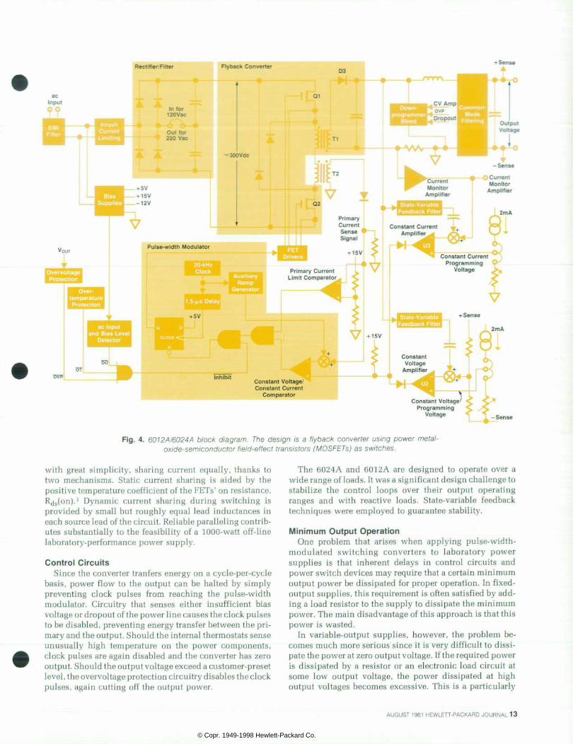
Swi tch ing Technology The basic topology used in the 6024 A and 60 12 A is the
flyback converter (see block diagram, Fig. 4). This topology allows ready control of how much energy is stored in the magnetic field of the power transformer during each clock cycle. The converter operates at constant frequency and regulation is achieved by pulse-width modulation. An operating frequency of 20 kHz allows a dramatic reduction in component size and weight from 60-Hz series-regulated technology, making the products lighter and easier to man
ufacture. The operating frequency is above the audible range but not high enough to cause power dissipation prob lems with fixed losses throughout the converter section.
The ac line is brought in through both common-mode and normal-mode EMI filtering. Bias voltages are developed with standard 60-Hz techniques, and power is provided to the inverter through the inrush current limiting section. (Inrush limiting is achieved with thermistors in the 6024A and with limiting resistors shunted by a relay in the 6012A). Following the inrush limiting circuitry is a rectifier/filter section, which is configured as a voltage doubler for 100/ 120Vac operation and as a bridge for 220/240Vac operation. An unregulated dc bus voltage of approximately 300 volts is developed at the output of the rectifier/filter section.
Power FETs Ql and Q2 are in series and are operated in-phase. The FETs are turned on by the pulse-width mod ulator, initiating linear current buildup in the magnetizing inductance of power transformer Tl. Thus energy is stored in the magnetic field of Tl. The primary current of Tl is monitored through current transformer T2 and fed back to the pulse-width modulator as the timing ramp. This timing ramp is compared to the error voltage from either the con stant voltage or the constant current control loop, and is also compared to a maximum primary current limit. When the primary current exceeds the lowest of these error volt ages, the pulse-width modulator turns off the FETs, inter rupting the primary current of transformer Tl. The voltage across Tl reverses polarity as a result of the collapsing magnetic field and forces diode D3 to conduct, transferring energy through the output filter to the load. Error amplifiers U2 and U3 maintain either constant voltage or constant cur rent operation by regulating the pulse width of the converter.
The use of the magnetizing current of Tl as the timing ramp for the pulse- width modulator improves the stability of the control loops. It also provides a convenient method of setting both a static and a dynamic limit on how much primary current will be allowed. This translates to defining the maximum output boundary as well as limiting the peak current in each of the power switches Ql and Q2.
Power FETs The use of power FETs for switches Ql and Q2 provides
many technical benefits that translate into customer fea tures. For one, the turn-on and turn-off response of the FETs can be made quite rapid by driver circuit design, allowing operation at very small pulse widths (<100 ns), which occur at low output power (light load). This is particularly advantageous in a laboratory supply where bizarre behavior at light loading is undesirable.
In switching rapidly the power FETs dissipate almost an order of magnitude less power in switching loss than a bipolar transistor of similar ratings. In addition, the switch ing speed can be controlled from the gate, allowing EMI and switching loss to be easily predicted and controlled. The FETs exhibit no secondary breakdown phenomenon, thereby eliminating the need for snubber networks and their power dissipation. The FETs require insignificant static drive power and require energy supplied to the gate only during switching transistions. Therefore, the drive circuits can be simple, efficient, and reliable.
Another aspect of power MOSFETs is that they parallel
1 2 H E W L E T T - P A C K A R D J O U R N A L A U G U S T 1 9 8 1
© Copr. 1949-1998 Hewlett-Packard Co.
Rec t i f i e r F i l t e r F l y b a c k C o n v e r t e r i - Sense D3
I n f o r 120Vac
O u t f o r 2 2 0 V a c
Q 1
C o m m o n - M o d e
T1
= 3 0 0 V d c
VOUT
Overvol tage P r o t e c t i o n
Over - t e m p e r a t u r e
P r o t e c t i o n
P u l s e - w i d t h M o d u l a t o r
+ 5V
ÃœVP
Auxil iary R a m p
rator
I n h i b i t
C o n s t a n t C u r r e n t P r o g r a m m i n g
V o l t a g e P r i m a r y C u r r e n t L i m i t C o m p a r a t o r
C o n s t a n t V o l t a g e / C o n s t a n t C u r r e n t
C o m p a r a t o r C o n s t a n t V o l t a g e '
P r o g r a m m i n g V o l t a g e - S e n s e
F i g . 4 . m e t a l - b l o c k d i a g r a m . T h e d e s i g n i s a f l y b a c k c o n v e r t e r u s i n g p o w e r m e t a l - ox ide-semiconductor f ie ld-ef fect t rans is tors (MOSFETs) as swi tches.
with great simplicity, sharing current equally, thanks to two mechanisms. Static current sharing is aided by the positive temperature coefficient of the FETs' on resistance, Rds(on).1 Dynamic current sharing during switching is provided by small but roughly equal lead inductances in each source lead of the circuit. Reliable paralleling contrib utes substantially to the feasibility of a 1000-watt off-line laboratory-performance power supply.
Control Circuits Since the converter tranfers energy on a cycle-per-cycle
basis, power flow to the output can be halted by simply preventing clock pulses from reaching the pulse-width modulator. Circuitry that senses either insufficient bias voltage or dropout of the power line causes the clock pulses to be disabled, preventing energy transfer between the pri mary and the output. Should the internal thermostats sense unusually high temperature on the power components, clock pulses are again disabled and the converter has zero output. Should the output voltage exceed a customer-preset level, the overvoltage protection circuitry disables the clock pulses, again cutting off the output power.
The 6024A and 601 2 A are designed to operate over a wide range of loads. It was a significant design challenge to stabilize the control loops over their output operating ranges and with reactive loads. State-variable feedback techniques were employed to guarantee stability.
Minimum Output Operat ion One problem that arises when applying pulse-width-
modulated switching converters to laboratory power supplies is that inherent delays in control circuits and power switch devices may require that a certain minimum output power be dissipated for proper operation. In fixed- output supplies, this requirement is often satisfied by add ing a load resistor to the supply to dissipate the minimum power. The main disadvantage of this approach is that this power is wasted.
In variable-output supplies, however, the problem be comes much more serious since it is very difficult to dissi pate the power at zero output voltage. If the required power is dissipated by a resistor or an electronic load circuit at some low output voltage, the power dissipated at high output voltages becomes excessive. This is a particularly
AUGUST 1981 HEWLETT-PACKARD JOURNAL 13
© Copr. 1949-1998 Hewlett-Packard Co.

Auxil iary Ramp
IP Ramp (Ful l Power)
Control Vol tage
Timing Ramp
PWM Output
Med ium Output Power
Control Vol tage
T iming Ramp
PWM Output
Low Output Power
Fig . 5 . An aux i l ia ry t iming ramp added to the pr imary t iming ramp takes effect at low output power so that very narrow, yet c o n t r o l l e d p u l s e w i d t h s a r e p r o d u c e d b y t h e p u l s e - w i d t h modulator (PWM) that switches the MOSFETs on and off . This a l lows e f f i c ien t opera t ion a t combinat ions o f low output vo l t age and cur rent .
nasty problem for autoranging supplies that experience large variations in output voltage.
Therefore, it was an important goal in the 6024A and 6012A to employ control circuit techniques and power de vices that would allow the generation of very narrow, yet controlled pulse widths in the power converter, so that operation at combinations of low output voltage and cur rent could be obtained with no output bleed.
The method employed to control the on time of the power FETs is to turn on the pulse-width modulator at the begin ning of every clock cycle and turn it off when a timing ramp exceeds a control voltage. The timing ramp is a voltage signal that is proportional to the converter primary current, and the control voltage is the error voltage from the con trol loops.
Any delay (Ta) from the time when the timing ramp ex ceeds the control voltage to when the power switch turns off causes the primary current to increase beyond the desired value and transfer more energy to the output than required.
For moderate and high output power, the control loops sense this condition and react by lowering the control volt age until the required on time is achieved. However, for low output power, this correction cannot occur, since the on time cannot be less than the value of the delay (Tj).
The delay consists of contributions from the comparator used to compare the ramp with the control voltage, the pulse-width modulator circuits, the power switch driver circuits, and the turn-off delay of the power switch itself. This delay is minimized by using high-speed comparators, pulse-width modulator logic, and driver circuits. In addi tion, the use of power MOSFETs rather than bipolar transis tors significantly reduces the turn-off delay of the power switch. These steps reduce the effect of the delay, but do not eliminate it.
To make it possible to control the on time even when it is very small or zero, an auxiliary ramp is derived from the clock circuit and added to the primary current timing ramp. Two key features of this auxiliary ramp are that it starts at least Tj earlier than the time the clock turns on the pulse- width modulator, and that its amplitude is limited to a low value to restrict its operation to small on times (see Fig. 5).
For large on times, the auxiliary ramp does not signifi cantly affect circuit operation. However, for very small on times, the pulse timing is determined entirely by the aux iliary ramp. For very low values of control voltage, the auxiliary ramp can exceed the control voltage and start the turn-off process be/ore the clock turns on the pulse-width modulator. In this way, the pulse-width modulator can produce very narrow pulses in the power converter and eliminate the need for a minimum output bleed.
Downprogrammer The 6024A and 6012 A are expected to be used as stimulus
sources in many automatic test and industrial processes. Throughput is quite important in most of these applica tions. Accordingly, particular attention was given to the programming speed of these supplies.
The problem of rapidly decreasing the output voltage is accentuated by the fact that these are laboratory switching supplies. To meet the fairly stringent output noise specifi cations requires a great deal of filtering, resulting in a large capacitance across the output terminals, up to 10,000 /J.F in the 601 2 A. To change the capacitor voltage rapidly implies a considerable amount of available charging and discharg ing current. The charging current for up-programming is quite naturally available from the power mesh itself. How ever, other than the external load, which is unpredictable, there is no inherently available source of appreciable dis charge current for downprogramming. Special circuitry had to he employed to meet the programming speed objec tives.
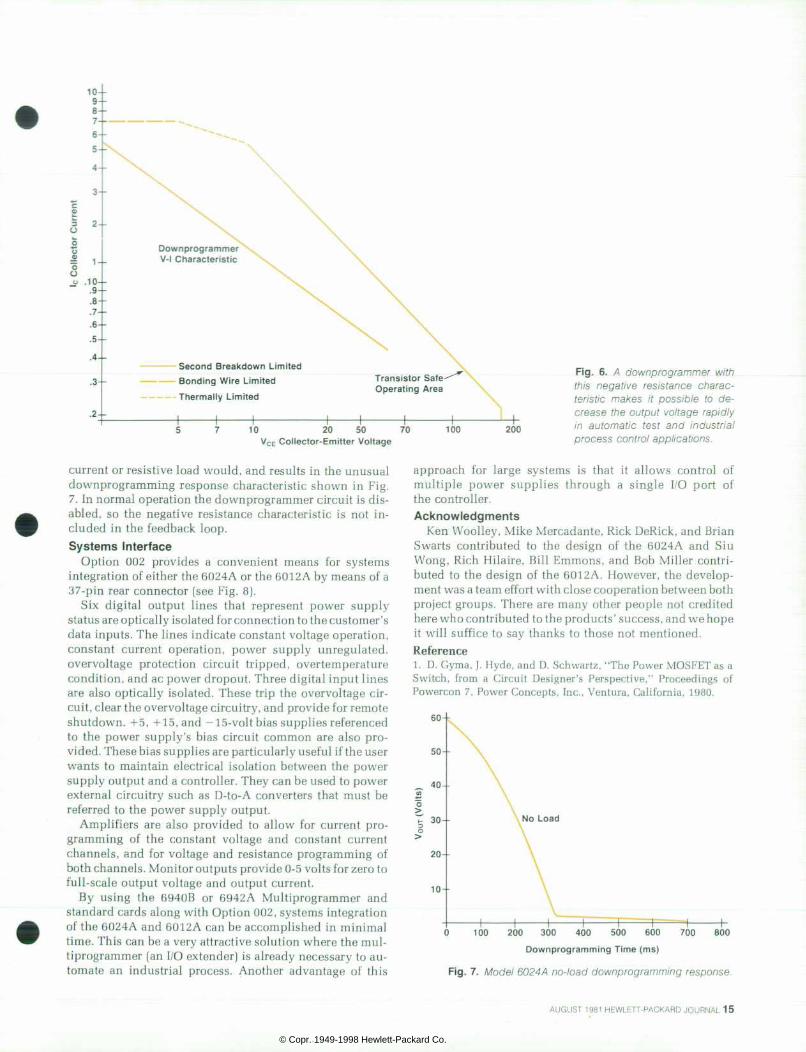
To achieve rapid downprogramming, a power transistor actively discharges the output capacitor. The discharge current is made a function of output voltage to take full advantage of the transistor's safe operating area and to en sure protection from secondary breakdown. The circuit pulls increasingly more current at lower output voltages, giving the downprogrammer circuit an overall negative resistance characteristic (see Fig. 6). This circuit implemen tation achieves faster downprogramming than a constant
' l 4 HEWLETT-PACKARD JOURNAL AUGUST 1981
© Copr. 1949-1998 Hewlett-Packard Co.
10 9- - 8- - 7- -- 6- - r -
4- -
: -
o o u .10
.9 6
.7
.6
-5
.4- -
. 3 - -
.2--
D o w n p r o g r a m m e r V - l Cha rac te r i s t i c
T r a n s i s t o r S a f e O p e r a t i n g A r e a
S e c o n d B r e a k d o w n L i m i t e d B o n d i n g W i r e L i m i t e d T h e r m a l l y L i m i t e d
- 1 0 2 0 5 0
VCE Co l lec to r -Emi t te r Vo l tage 100 2 0 0
F i g . 6 . A d o w n p r o g r a m m e r w i t h t h i s n e g a t i v e r e s i s t a n c e c h a r a c t e r i s t i c m a k e s i t p o s s i b l e t o d e crease the output vo l tage rap id ly i n a u t o m a t i c t e s t a n d i n d u s t r i a l process contro l appl icat ions.
current or resistive load would, and results in the unusual downprogramming response characteristic shown in Fig. 7. In normal operation the downprogrammer circuit is dis abled, so the negative resistance characteristic is not in cluded in the feedback loop. Systems Interface
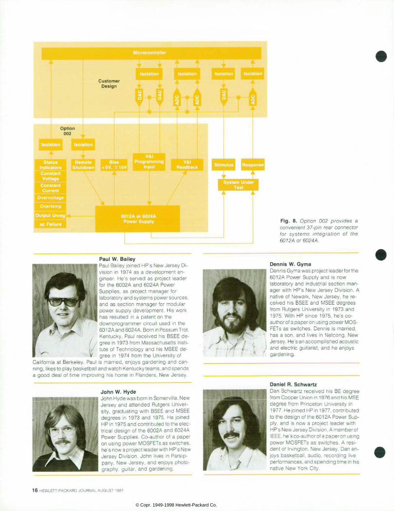
Option 002 provides a convenient means for systems integration of either the 6024A or the 6012A by means of a 37-pin rear connector (see Fig. 8).
Six digital output lines that represent power supply status are optically isolated for connection to the customer's data inputs. The lines indicate constant voltage operation, constant current operation, power supply unregulated, overvoltage protection circuit tripped, overtemperature condition, and ac power dropout. Three digital input lines are also optically isolated. These trip the overvoltage cir cuit, clear the overvoltage circuitry, and provide for remote shutdown. +5, +15, and -15-volt bias supplies referenced to the power supply's bias circuit common are also pro vided. These bias supplies are particularly useful if the user wants to maintain electrical isolation between the power supply output and a controller. They can be used to power external circuitry such as D-to-A converters that must be referred to the power supply output.
Amplifiers are also provided to allow for current pro gramming of the constant voltage and constant current channels, and for voltage and resistance programming of both channels. Monitor outputs provide 0-5 volts for zero to full-scale output voltage and output current.
By using the 6940B or 6942A Multiprogrammer and standard cards along with Option 002, systems integration of the 6024A and 6012A can be accomplished in minimal time. This can be a very attractive solution where the mul- tiprogrammer (an I/O extender) is already necessary to au tomate an industrial process. Another advantage of this
approach for large systems is that it allows control of multiple power supplies through a single I/O port of the controller. Acknowledgments
Ken Woolley, Mike Mercadante, Rick DeRick, and Brian Swarts contributed to the design of the 6024A and Siu Wong, Rich Hilaire, Bill Emmons, and Bob Miller contri buted to the design of the 6012A. However, the develop ment was a team effort with close cooperation between both project groups. There are many other people not credited here who contributed to the products' success, and we hope it will suffice to say thanks to those not mentioned. Reference 1. D. Gyma, J. Hyde, and D. Schwartz, "The Power MOSFET as a Switch, from a Circuit Designer's Perspective," Proceedings of Powercon 7, Power Concepts, Inc., Ventura, California, 1980.
6 0 - -
100 2 0 0 3 0 0 4 0 0 5 0 0 6 0 0
Downprogramming T ime (ms)
7 0 0 8 0 0
F ig . 7 . Mode l 6024A no- load downprogramming response .
AUGUST 1981 HEWLETT-PACKARD JOURNAL 15
© Copr. 1949-1998 Hewlett-Packard Co.
Customer Design
Option 002
Status Indicators Constant Vol tage
Constant Current
Overvol tage
Over temp
Remote Shutdown
Bias + 5V, ±15V
V&l Programming
Input V&l
Readback Response
System Under Test
6 0 1 2 A o r 6 0 2 4 A Power Supply F i g . 8 . O p t i o n 0 0 2 p r o v i d e s a
conven ient 37-p in rear connector f o r s y s t e m s i n t e g r a t i o n o f t h e 6 0 1 2 A o r 6 0 2 4 A .
P a u l W . B a i l e y I Paul Bai ley joined HP's New Jersey Di v i s ion i n 1974 as a deve lopmen t en g ineer . He 's served as pro jec t leader fo r the 6002A and 6024A Power
I Suppl ies , as pro ject manager for laboratory and systems power sources, and as sec t ion manager fo r modu la r power supp ly deve lopment . H is work
• has resulted in a patent on the : * d o w n p r o g r a m m e r c i r c u i t u s e d i n t h e
f ' ' * Â ¿ * 6 0 1 2 A a n d 6 0 2 4 A . B o r n i n P o s s u m T r o t , Kentucky, Pau l rece ived h is BSEE de-
( g r e e i n 1 9 7 3 f r o m M a s s a c h u s e t t s I n s t i tu te o f Techno logy and h is MSEE de-
w g r e e i n 1 9 7 4 f r o m t h e U n i v e r s i t y o f Ca l i fo rn ia a t Berke ley . Pau l i s mar r ied , en joys garden ing and can ning, l ikes to play basketbal l and watch Kentucky teams, and spends a good dea l o f t ime improv ing h is home in F landers , New Jersey .
J o h n W . H y d e John Hyde was born in Somervi l le, New Je rsey and a t t ended Ru tge rs Un i ve r s i ty , g raduat ing wi th BSEE and MSEE degrees in 1973 and 1975. He jo ined HP in 1 975 and contr ibuted to the elec t r i ca l des ign o f the 6002A and 6024A Power Suppl ies . Co-author o f a paper
I on us ing power MOSFETs as swi tches, I he's now a project leader with HP's New
Jersey Div is ion. John l ives in Pars lp- pany , New Je rsey , and en joys pho to g raphy , gu i ta r , and garden ing .
Dennis W. Gyma Dennis Gyma was project leader for the 601 2A Power Supply and is now labora tory and indus t r ia l sec t ion man ager wi th HP's New Jersey Div is ion. A na t i ve o f Newark , New Jersey , he re ce ived h is BSEE and MSEE degrees f rom Rutgers Univers i ty in 1973 and 1975. Wi th HP s ince 1975 , he 's co author of a paper on using power MOS FETs as swi tches. Dennis is marr ied, has a son, and l i ves in Netcong, New Jersey. He's an accompl ished acoust ic and e lect r ic gu i tar is t , and he enjoys gardening.
Daniel R. Schwartz Dan Schwar tz rece ived h is BE degree from Cooper Union in 1 976 and his MSE degree f rom Pr inceton Univers i ty in 1 977. He joined HP in 1 977, contributed to the design of the 601 2A Power Sup p ly , and is now a pro jec t leader w i th HP's New Jersey Division. A member of IEEE, he's co-author of a paper on using power MOSFETs as sw i t ches . A res i dent o f I rv ington, New Jersey, Dan en joys basketbal l , audio, record ing l ive performances, and spending t ime in his nat ive New York Ci ty .
1 6 H E W L E T T - P A C K A R D J O U R N A L A U G U S T 1 9 8 1
© Copr. 1949-1998 Hewlett-Packard Co.

S P E C I F I C A T I O N S HP 65000A Se r i es SOW Power Supp l i es
•V1 is the Main Output. V2 and V3 are semi-regulated extra outputs. V4, V5, and V6 are adjustable over the range g iven.
INPUT VOLTAGE: 87 -127Vac /174-250Vac , 47 -63 Hz TEMPERATURE OPERATING: 0-50°C convect ion cooled
0-70°C fan cooled STORAGE: -20 to 85°C CARRYOVER TIME: 25 ms min imum a t 1 15 o r 230Vac
10 ms min imum a t 104 o r 208Vac EFFICIENCY: 70 to 76% typ ica l REMOTE SHUTDOWN: La tch ing shu tdown v iaTTL pu l se REMOTE SENSE: V1 only , ±5% range. OUTPUT DRIFT: 0 .25% max imum 8 h rs a f te r 1 -hour warmup OVERTEMPERATURE: 80±5IC automat ic shutdown SAFETY RECOGNIT IONS: UL478 , UL114 , CSA 22 .2 /143 and CSA 22 .2 /154 SAFETY DESIGN TO: VDE 0730 /2P and IEC348 EMI: VDE 0871 Class B wi th external cover and f i l ter OVERCURRENT PROTECTION: Al l outputs protected, V1 and V4-V6 thermal ly protected,
V2-V3 fused. O V E R V O L T A G E P R O T E C T I O N : V 1 a n d V 4 - V 6 a u t o m a t i c s h u t d o w n , V 2 - V 3 v o l t a g e
clamped. O T H E R O U T P U T S P E C I F I C A T I O N S ( W O R S T O F A L L M O D E L S )
PRICES IN U.S.A.: Single Output S ing le - r 2 Outputs T r ip le + 2 Outpu ts Quadrup le + 2 Outpu ts
Unit 1000 qty.
$195 $154
$240 $190
$255 $201
$265 $209
HP Model 6024A Power Supply - 200W
DC OUTPUT: Vo l t age and cu r ren t ou tpu t can be ad jus ted ove r t he range i nd i ca ted by using f ront-panel controls, analog programming, or opt ional system inter face. V O L T A G E : 0 - 6 0 V C U R R E N T : 0 - 1 0 A
Maximum avai lab le output power f rom 20V to 60V is ind icated in F ig . 3 on page 12. LOAD EFFECT: (Load Regu la t ion) :
V O L T A G E : 0 . 0 1 % + 3 m V C U R R E N T : 0 . 0 1 % + 3 m A S O U R C E E F F E C T :
V O L T A G E ; 0 . 0 1 % + 2 m V C U R R E N T : 0 . 0 1 % + 2 m A PARD (Ripp le and Noise) rms/p-p . 20 Hz to 20 MHz:
V O L T A G E : 3 m V / 3 0 m V C U R R E N T : 5 m A r m s TEMPERATURE COEFFICIENT: A/°C af ter 30-minute warmup:
V O L T A G E : 0 . 0 1 % + 1 m V C U R R E N T : 0 . 0 3 % + 1 m V
DRIFT: Stab ik ty) change in output over an 8-hour in terva l . V O L T A G E : 0 . 0 3 % - 3 m V C U R R E N T : 0 . 0 3 %
R E M O T E C O N T R O L ( A N A L O G P R O G R A M M I N G ) : Resistance necessary for ful l -scale output of :
V O L T A G E : 2 5 0 0 0 A C C U R A C Y : 0 . 8 % - 1 m V
Voltage necessary for fu l l -scale output of : VOLTAGE: 5 vo l t s A C C U R A C Y : 0 . 2 % - m V
C U R R E N T : 2 5 0 0 0 A C C U R A C Y : 2 . 4 %
3 m V
1 mA
C U R R E N T : 5 v o l t s A C C U R A C Y : 0 . 9 % * 1 m A
P R O G R A M M I N G R E S P O N S E T I M E : M a x i m u m t i m e f o r o u t p u t v o l t a g e t o c h a n g e f r o m 0V to 60V of 60V to 2V and set t le w i th in 60 mV. U P : F u l l L o a d ( 1 8 Ã 1 ) 2 0 0 m s D O W N : F u l l L o a d ( 1 8 Ã 1 ) 3 0 0 m s
N o L o a d 2 0 0 m s N o L o a d 6 0 0 m s OVERVOLTAGE PROTECTION: T r ip vo l tage ad jus tab le f rom 2 to 64 vo te . AMPLIF IED CURRENT MONITOR: 0 -5V mon i to r ou tpu t fo r 0 -10A ou tpu t . EMI SPECIFICATIONS: Meets VDE 0871/6 .78 Leve l A . SAFETY SPECIF ICATIONS: Comp l i es w i t h IEC 348 . VDE 0411 , CSA 556B . CSA C22 .2
#0-1975. TEMPERATURE: OPERATING: 0 t o SS 'C .
STORAGE: -40 to +75°C. AC INPUT: 104-127Vac 48-63 Hz , 5 .3A rms max imum. WEIGHT: Net 5.4 kg (12 Ib) . Shipping 7.3 kg (16 Ib) . SYSTEM INTERFACE OPTION: Same as system inter face opt ion for 6012A except vol tage
accuracy i s 0 .3% + 7 mV and cur ren t accuracy i s 1% + 2 mA. PRICES IN U.S.A. :
6024A Power Supp ly , $875. Opt ion 002: System Inter face, $300. Opt ion 100: 87-106Vac, 48-63 Hz, N/C. (Output derated to 50V, 150W.) Opt ion 220: 191-233V3C, 48-63 Hz, N/C. Opt ion 240: 208-250Vac, 48-63 Hz, N/C.
HP Model 6012A Power Supply - 1000W
DC OUTPUT: Vo l t age and cu r ren t ou tpu t can be ad jus ted ove r t he range i nd i ca ted by using f ront-panel contro ls, analog programming, or opt ional system inter face. V O L T A G E : 0 - 6 0 V C U R R E N T : 0 - 5 0 A
Maximum avai lab le output power f rom 20V to 60V is ind icated in F ig . 3 on page 12. LOAD EFFECT: (Load Regu la t ion) :
V O L T A G E : 0 . 0 1 % + 5 m V C U R R E N T : 0 . 0 1 % + 5 m A S O U R C E E F F E C T :
V O L T A G E : 0 . 0 1 % + 3 m V C U R R E N T : 0 . 0 1 % + 5 m A PARD (Ripp le and Noise) rms/p-p . 20 Hz to 20 MHz:
V O L T A G E : 5 m V / 5 0 m V C U R R E N T : 2 5 m A r m s TEMPERATURE COEFFICIENT: 4 /°C af ter 30-minute warmup:
V O L T A G E : 0 . 0 1 % + 2 m V C U R R E N T : 0 . 0 1 % + 3 m A DRIFT: (Stabi l i ty) change in output over an 8-hour interval .
V O L T A G E : 0 . 0 3 % + 5 m V C U R R E N T : 0 . 0 3 % + 5 m A R E M O T E C O N T R O L ( A N A L O G P R O G R A M M I N G ) :
Resistance necessary for fu l l scale output of : V O L T A G E : 2 5 0 0 Ã 1 C U R R E N T : 2 5 0 0 1 1 A C C U R A C Y : 1 % + 3 m V A C C U R A C Y : 2 . 5 % + 1 0 m A
Voltage necessary for fu l l -scale output of : VOLTAGE: 5 vo l t s A C C U R A C Y : 0 . 3 % + 3 m V
CURRENT: 5 vo l t s A C C U R A C Y : 1 % + 1 0 m A
P R O G R A M M I N G R E S P O N S E T I M E : M a x i m u m t i m e f o r o u t p u t v o l t a g e t o c h a n g e f r o m 0V to 60V or 60V to 2V and set t le wi th in 200 mV. U P : F u l l L o a d ( 3 . 4 ! ! ) 1 2 0 m s D O W N : F u l l L o a d ( 3 . 4 n ) 4 0 0 m s
N o L o a d 1 2 0 m s N o L o a d 1 . 2 s OVERVOLTAGE PROTECTION: Tr ip vo l tage ad jus tab le f rom 2 to 60 vo l t s . AMPLIF IED CURRENT MONITOR: 0 -5V mon i to r ou tpu t fo r 0 -50A ou tpu t . EMI SPECIFICATIONS: Meets VDE 0871/6 .78 Leve l A . SAFETY SPECIF ICAT IONS: Comp l i es w i t h IEC 348 , VDE 0411 , CSA 556B , CSA C22 .2
#0-1975. TEMPERATURE: OPERATING: 0 to 50°C.
STORAGE: -40 to +75°C. AC INPUT: 104-127V3C 48-63 Hz, 24A rms max imum. WEIGHT: Net 15 kg (33 Ib) . Shipp ing 16 kg (35 Ib) . S Y S T E M I N T E R F A C E O P T I O N R E M O T E C O N T R O L ( A N A L O G P R O G R A M M I N G ) :
Sink current necessary for ful l scale of : V O L T A G E : 2 m A C U R R E N T : 2 m A A C C U R A C Y : 0 . 4 % + 9 m V A C C U R A C Y : 1 . 1 % + 1 5 m A
ISOLATION: S ta tus and con t ro l l i nes : 600Vdc max f rom equ ipmen t g round , f r om the power supply output or f rom each other .
PRICES IN U.S.A. : 6012A Power Supp ly , $1550. Opt ion 002: System Inter face, $300. Opt ion 100: 90-105Vac, 48-63 Hz. N/C. (Output derated to 50V, 750W.) Opt ion 220: 191-233Vac. 48-63 Hz, N/C. Opt ion 240: 208-250Vac, 48-63 Hz, N/C.
MANUFACTURING D IV IS ION: NEW JERSEY D IV IS ION Green Pond Road Rockaway, New Jersey 07866 U.S.A.
AUGUST 1981 HEWLETT-PACKARD JOURNAL 17
© Copr. 1949-1998 Hewlett-Packard Co.
The Vert ical Power MOSFET for High-Speed Power Control A vert ical semiconductor device structure provides a power MOSFET that can swi tch h igh cur rents and vo l tages very rap id ly . Th is makes i t usefu l fo r power suppl ies , pu lse dr ivers, and swi tch ing ampl i f iers.
by Kar l H. T iefer t , Dah Wen Tsang, Robert L . Myers, and Victor L i
POWER AND FREQUENCY are natural electronic enemies. In a variety of detailed technical ways, as well as in fundamental ones, the speed of operation
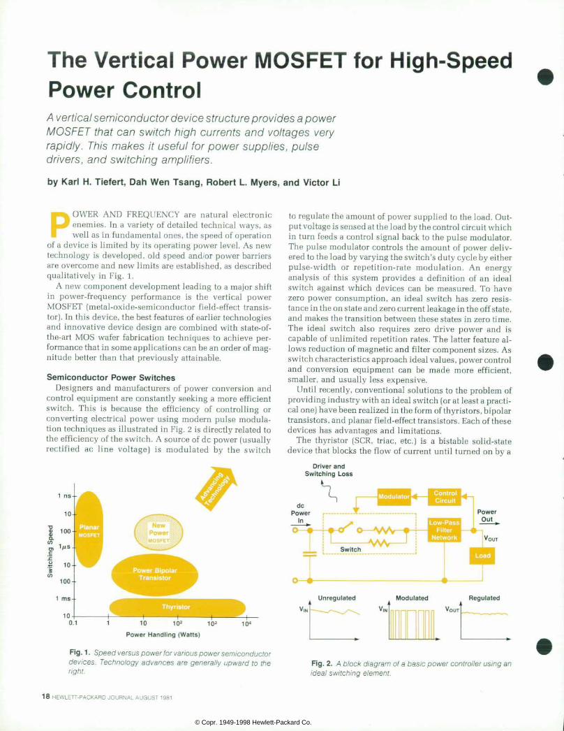
of a device is limited by its operating power level. As new technology is developed, old speed and/or power barriers are overcome and new limits are established, as described qualitatively in Fig. 1.
A new component development leading to a major shift in power-frequency performance is the vertical power MOSFET (metal-oxide-semiconductor field-effect transis tor). In this device, the best features of earlier technologies and innovative device design are combined with state-of- the-art MOS wafer fabrication techniques to achieve per formance that in some applications can be an order of mag nitude better than that previously attainable.
Semiconductor Power Swi tches Designers and manufacturers of power conversion and
control equipment are constantly seeking a more efficient switch. This is because the efficiency of controlling or converting electrical power using modern pulse modula tion to as illustrated in Fig. 2 is directly related to the efficiency of the switch. A source of dc power (usually rectified ac line voltage) is modulated by the switch
Power Bipolar Transistor
I 1 0 1 0 2
Power Handl ing (Watts)
—I — 103 104
Fig. 1 . Speed versus power for var ious power semiconductor dev ices . Techno logy advances a re genera l l y upward to the right.
to regulate the amount of power supplied to the load. Out put voltage is sensed at the load by the control circuit which in turn feeds a control signal back to the pulse modulator. The pulse modulator controls the amount of power deliv ered to the load by varying the switch's duty cycle by either pulse-width or repetition-rate modulation. An energy analysis of this system provides a definition of an ideal switch against which devices can be measured. To have zero power consumption, an ideal switch has zero resis tance in the on state and zero current leakage in the off state, and makes the transition between these states in zero time. The ideal switch also requires zero drive power and is capable of unlimited repetition rates. The latter feature al lows reduction of magnetic and filter component sizes. As switch characteristics approach ideal values, power control and conversion equipment can be made more efficient, smaller, and usually less expensive.
Until recently, conventional solutions to the problem of providing industry with an ideal switch (or at least a practi cal one) have been realized in the form of thyristors, bipolar transistors, and planar field-effect transistors. Each of these devices has advantages and limitations.
The thyristor (SCR, triac, etc.) is a bistable solid-state device that blocks the flow of current until turned on by a
Driver and Switching Loss
VIN
Unregulated Modulated Regulated
Fig. 2 . A b lock d iagram of a bas ic power cont ro l ler us ing an ideal swi tching element.
1 8 H E W L E T T - P A C K A R D J O U R N A L A U G U S T 1 9 8 1
© Copr. 1949-1998 Hewlett-Packard Co.
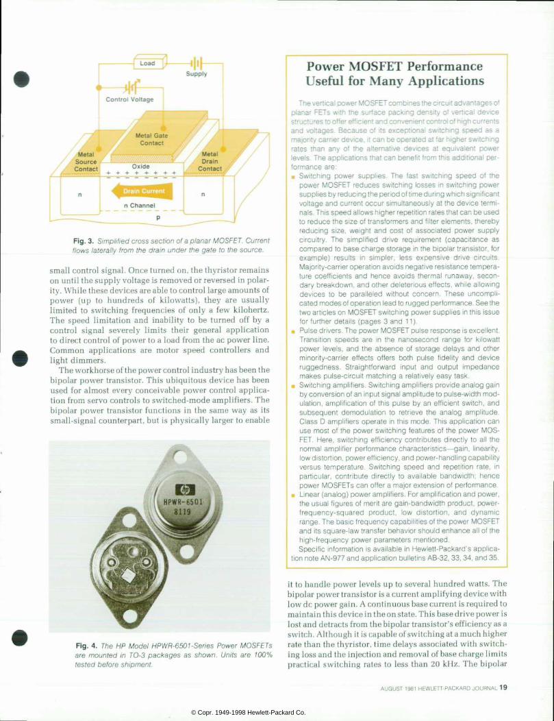
Control Voltage
Fig. 3. Simpl i f ied cross sect ion of a p lanar MOSFET. Current f lows latera l ly f rom the dra in under the gate to the source.
small control signal. Once turned on, the thyristor remains on until the supply voltage is removed or reversed in polar ity. While these devices are able to control large amounts of power (up to hundreds of kilowatts), they are usually limited to switching frequencies of only a few kilohertz. The speed limitation and inability to be turned off by a control signal severely limits their general application to direct control of power to a load from the ac power line. Common applications are motor speed controllers and light dimmers.
The workhorse of the power control industry has been the bipolar power transistor. This ubiquitous device has been used for almost every conceivable power control applica tion from servo controls to switched-mode amplifiers. The bipolar power transistor functions in the same way as its small-signal counterpart, but is physically larger to enable
Power MOSFET Performance Useful for Many Applications
The vert ical power MOSFET combines the circuit advantages of p lanar FETs wi th the sur face pack ing dens i ty o f ver t ica l dev ice structures to offer eff icient and convenient control of high currents and vo l tages . Because o f i t s except iona l sw i tch ing speed as a major i ty carr ier device, i t can be operated at far higher switching ra tes t han any o f t he a l t e rna t i ve dev i ces a t equ i va len t power levels. The appl icat ions that can benef i t f rom th is addi t ional per formance are: * S w i t c h i n g p o w e r s u p p l i e s . T h e f a s t s w i t c h i n g s p e e d o f t h e
power MOSFET reduces swi tch ing losses in swi tch ing power supplies by reducing the period of t ime during which signif icant vo l tage and cur rent occur s imul taneous ly a t the dev ice termi nals. This speed allows higher repetit ion rates that can be used to reduce the size of t ransformers and f i l ter elements, thereby reduc ing s i ze , we igh t and cos t o f assoc ia ted power supp l y c i r cu i t r y . The s imp l i f i ed d r i ve requ i remen t ( capac i t ance as compared to base charge storage in the bipolar t ransistor , for e x a m p l e ) r e s u l t s i n s i m p l e r , l e s s e x p e n s i v e d r i v e c i r c u i t s . Major i ty-carr ier operat ion avoids negat ive resistance tempera tu re coe f f i c i en ts and hence avo ids the rma l runaway , secon dary breakdown, and other deleter ious ef fects, whi le a l lowing d e v i c e s t o b e p a r a l l e l e d w i t h o u t c o n c e r n . T h e s e u n c o m p l i cated modes of operat ion lead to rugged performance. See the two art ic les on MOSFET switching power suppl ies in this issue for fur ther deta i ls (pages 3 and 11) .
. Pulse dr ivers. The power MOSFET pulse response is excel lent. T rans i t i on speeds a re i n the nanosecond range fo r k i l owa t t power l eve l s , and the absence o f s to rage de lays and o the r m inor i t y -car r ie r e f fec ts o f fe rs bo th pu lse f ide l i t y and dev ice r u g g e d n e s s . S t r a i g h t f o r w a r d i n p u t a n d o u t p u t i m p e d a n c e makes pulse-c i rcu i t matching a re lat ive ly easy task. Switching ampl i f iers. Switching ampl i f iers provide analog gain by conversion of an input s ignal ampl i tude to pulse-width mod u lat ion, ampl i f icat ion of th is pu lse by an ef f ic ient swi tch, and subsequen t demodu la t ion to re t r i eve the ana log amp l i t ude . Class D ampl i f iers operate in th is mode. This appl icat ion can use most o f the power sw i tch ing fea tu res o f the power MOS FET . t he sw i t ch ing e f f i c i ency con t r i bu tes d i r ec t l y t o a l l t he normal amplif ier performance characterist ics — gain, l inearity, low distort ion, power ef f ic iency, and power-handl ing capabi l i ty ve rsus tempera tu re . Swi tch ing speed and repe t i t i on ra te , in par t i cu la r , con t r ibu te d i rec t l y to ava i lab le bandwid th ; hence power MOSFETs can of fer a major extension of per formance.
• Linear (analog) power amplif iers. For amplif ication and power, the usual f igures of mer i t are gain-bandwidth product , power- f r e q u e n c y - s q u a r e d p r o d u c t , l o w d i s t o r t i o n , a n d d y n a m i c range. The basic f requency capabi l i t ies of the power MOSFET and i ts square- law transfer behavior should enhance al l of the h igh- f requency power parameters ment ioned. Speci f ic in format ion is avai lab le in Hewlet t -Packard 's appl ica
t ion 35. AN-977 and appl icat ion bul let ins AB-32, 33, 34, and 35.
Fig . 4 . The HP Model HPWR-6501 -Ser ies Power MOSFETs a r e m o u n t e d i n T O - 3 p a c k a g e s a s s h o w n . U n i t s a r e 1 0 0 % tested before shipment.
it to handle power levels up to several hundred watts. The bipolar power transistor is a current amplifying device with low dc power gain. A continuous base current is required to maintain this device in the on state. This base drive power is lost a detracts from the bipolar transistor's efficiency as a switch. Although it is capable of switching at a much higher rate than the thyristor, time delays associated with switch ing loss and the injection and removal of base charge limits practical switching rates to less than 20 kHz. The bipolar
AUGUST 1981 HEWLETT-PACKARD JOURNAL 19
© Copr. 1949-1998 Hewlett-Packard Co.

Metal Gate Contact
n- type Source
p-type Substrate
Fig. 5. Simpl i f ied cross sect ion of a ver t ica l power MOSFET. The d ra in i s l oca ted on the bo t tom and the sou rce on top . Current f lows upward under the gate and then outward to the source regions.
power transistor also suffers from other disadvantages, such as potential thermal instability and secondary break down (a condition of destructive thermal runaway resulting from the simultaneous presence of high currents and high electric field), that restricts its ability to control power to a reactive load.
A third alternative is the planar MOSFET. This device comes very close to meeting two of the ideal switch's characteristics. As a voltage-controlled current device, an almost neglible amount of power is required to control the switching action of the MOSFET. Also, lacking the time delays inherent in a bipolar junction device, the planar MOSFET can easily be operated at frequencies up to hun dreds of megahertz. The operation of the planar MOSFET is shown in Fig. 3. The flow of current through the channel is controlled by an electric field that is generated by a voltage applied to the gate terminal. Since the gate is electrically insulated from the rest of the device, no dc current can flow to the gate and only a small amount of power is consumed in charging and discharging the gate capacitance during switching. Unfortunately, the current to be controlled is conducted laterally through a relatively long channel. This causes a significant voltage drop to appear between the drain and source terminals. The result is a high on resis tance of 10 to 100 ohms, a large departure from our ideal switch. This high on resistance causes an appreciable
power dissipation in the channel, thus limiting the use of the planar MOSFET as a switch to applications handling power of one watt or less.
Ver t ica l Power MOSFET Up to now, users of power semiconductors were faced
with selecting either power or speed: take your choice. The thyristor, while able to handle kilowatts of power, is gener ally limited to line-frequency control of ac power. The pla nar MOSFET is amazingly fast, but can only control about one watt of power. As a compromise, the bipolar power transistor offers a moderate power capability at inter mediate switching speeds.
Now, however, a new technology called vertical DMOS (double-diffused MOS) has combined bipolar power and MOSFET speed into one device. This device, the HP Model HPWR-6501-Series Power MOSFET (Fig. 4), has made the design of low-cost, reliable, and efficient power supplies possible (see article on page 3). Its basic operation is illus trated in Fig. 5. In contrast to the surface conduction path in the planar MOSFET, current flows vertically through the vertical DMOS device. This allows drain current to be col lected from the device substrate, removes the need to allow for drain contact area on the surface of the device, and in effect doubles the active gate area on the chip. Such in creases in packing density directly reduce the cost and improve the performance of the device. Like the planar MOSFET, the flow of drain current is controlled by a volt age applied to the gate terminal. A positive gate voltage causes a conductive channel to be induced in the p-type material immediately under the gate oxide layer. This channel allows a controlled amount of current to be con ducted from the drain to the source terminal. A vertical power MOSFET actually consists of thousands of these basic cells connected in parallel on a single chip of silicon.
How I t Works A simplified cross-section drawing illustrating some of
the principal elements of a Hewlett-Packard power MOS FET is shown in Fig. 6. The gated channels are to the left; the edge of the device is to the right. In the active region, an n-channel DMOS structure is used. The channel is defined by two consecutive thermal diffusion processes rather than *Edi tor 's Note: Throughout th is d iscussion reference is made to var ious impur i ty (doping) concent ra t ions by us ing the des ignat ions p- ,p ,p+,n- ,n , and n + . Acceptor impur i t ies are i nd i ca ted by p and donor impur i t i es by n . L igh t l y doped (concen t ra t i ons less than 10 ' s a toms/cm3) reg ions a re ind ica ted by the minus s ign and heav i l y doped (concen t ra t ions greater than 10" a toms/cm3) areas by the pos i t i ve s ign
Field Oxide Phosphorus
, Doped Oxide Pyrelyt ic Oxide Polysi l icon Gate
n - E p i t a x i a l L a y e r
n+ Subst ra te
Guard Rings
mmm
F i g . 6 . C r o s s s e c t i o n o f t h e H P ve r t i ca l power MOSFET show ing t h e g u a r d - r i n g s t r u c t u r e o n t h e r ight. This structure distr ibutes the e lect r ic f ie lds at and near the top surface to maintain a high vol tage breakdown capab i l i t y .
2 0 H E W L E T T - P A C K A R D J O U R N A L A U G U S T 1 9 8 1
© Copr. 1949-1998 Hewlett-Packard Co.

by photolithography, thereby producing a very well con trolled and very narrow channel length. The diffused chan nel has a graded impurity (doping) concentration that pre vents punchthrough voltage breakdown when a large drain-to-source voltage is applied. The short channel length reduces transit time and gives the DMOS device the high speed necessary for a fast switch. A full surface metal lization contacts both the n+ source region and the p-well on the top surface. Polycrystalline silicon is used for the gate electrode, which is insulated from the source metal by a sandwich structure of pyrogenic silicon dioxide, silicon nitride, and pyrolytic silicon dioxide layers and contacted at various places by the gate connection metal. The drain region is an n- epitaxial (epi) layer grown on an n+ sub strate. The substrate is contacted on the bottom surface by backside metal to form the ohmic contact. Current in the device flows laterally through the channel region and then vertically down through the epi layer.
Because of the presence of high electric fields near and at the surface, the periphery of the device must be protected against premature breakdown. This is done in the HP power MOSFET by adding specially designed guard rings as shown in Fig. 6. These guard rings function as voltage dividers to distribute the high voltage, which would other wise appear only across the main pn junction. This reduces the maximum field strength at the surface and at the dif fused cylindrical pn junctions.
Since conduction is by majority carriers in these devices, charge storage delay is insignificant compared to that for bipolar transistors. Under normal operating temperatures, current crowding and local hot spots do not occur because the thermal coefficient of resistivity is positive. Thus, the secondary breakdown phenomenon encountered in bipolar transistors is eliminated.
The vertical DMOS FET greatly improves the device packing density per unit area which results in other advan tages such as high-current handling capability and high transconductance. Some typical electrical characteristics for an HP device packaged in a TO-3 package are given in the specifications on page 23. The maximum current rating
©©0©©©0© Polysi l icon Gate COD
F ig . 7 . C ross -sec t i on o f a s ing le ce l l o f t he ve r t i ca l power MOSFET showing e lect ron f low and paras i t ic e lements.
is determined to a large extent by packaging limitations and not by the device.
Principles of Operation As the name MOSFET suggests, the flow of current is
controlled by an electric field. To illustrate this, let us look at Fig. 7 which is an enlargement of a single cell of the device structure shown in Fig. 6. Notice that, with the vertical arrangement, a polysilicon gate has two channel regions. The width of the polysilicon gate and the as sociated spacing between the two p wells are chosen to maximize packing density and minimize resistance. This is very different from the lateral arrangement, which not only uses up one side of the gate for a drain contact, but also requires a wider polysilicon gate to withstand the full drain-to-source voltage. Besides these savings in device active area, the large topside surface area, which otherwise would be wasted on a drain bonding pad and drain metal interconnections, can now be used to create more channels when the drain terminal is moved to the bottom of the chip. The result is a very efficient design that, compared to a lateral structure with the same device area, more than dou bles the transconductance and current handling capability while reducing the epitaxial-layer resistance by nearly half.
The formation of a conductive channel and electron flow is shown on the left-hand side of Fig. 7 while schematic circuit elements are indicated on the right. For normal operation, the drain-to-source voltage is positive. This places the pn drain-source diode in reverse bias, allowing only a minute reverse leakage current. However, if a con ductive channel is created along the silicon surface beneath the gate oxide, a large current can flow in the direction indicated.
When the drain-to-source voltage is negative, the drain pn junction is forward biased through the p diffusion and the source contact. In this condition drain-to-source current is simply that of the large diode junction and is unaffected by the gate. This feature is used to limit negative voltage excursions in some applications.
In normal operation a conductive channel can be created if the proper gate bias is applied. A negative gate bias attracts positive charges toward the silicon surface. For zero or negative gate bias, we encounter two pn junctions as we travel from source to drain under the gate. If a positive drain-to-source bias is applied, both of these junctions will be reverse biased, no current can flow, and the device is off.
If, on the other hand, a positive gate bias is applied, negative charges will gather under the gate. From source to drain, we see a continuous concentration of free electrons which forms a conduit for charge flow. The pn junctions that acted as barriers under a negative gate bias no longer exist because the p region under the gate is now turned into a thin n-type layer. The application of a drain-to-source field (or voltage) causes drain-to-source current and the device is on.
The amount of current depends on the gate potential applied and the extent to which electrons are attracted toward the surface. When the drain-to-source potential is small, the gate electrode has the predominant influence in the channel region underneath it, current is linear with applied drain-to-source voltage and the larger the gate po-
AUGUST 1981 HEWLETT-PACKARD JOURNAL 21
© Copr. 1949-1998 Hewlett-Packard Co.

tential, the lower the channel resistance will be. In MOS- FET terminology, this mode of operation is termed the "linear region." The interplay of the various potentials and the net current that results are summarized in the following equation:
DS l.t, VDS(VGs - VGS(th)) - (VDS)'
where W is the channel width, L is the channel length between drain and source, /u. is the surface electron mobil ity, e is the dielectric constant of the semiconductor mate rial, and tox is the gate oxide thickness. VDS and VGS are drain and gate voltages respectively, both referenced to the source. The quantity VGS(th), (termed the threshold volt age, a complex quantity encompassing the substrate dop ing, the nature of the oxide, and the semiconductor oxide interface] provides a measure of the gate potential required to cause sufficient electrons to be attracted to the surface for current conduction. This quantity can be tailored to suit the designer's or user's need.
This seemingly complex expression is quite straightfor ward to derive. The key is to account for the number of electrons attracted to the p-well surface by the effective gate potential while treating the gate-oxide-channel system as a capacitor. Then the conductivity of the channel can be estimated. The charge flow resulting from a drain-to-sourcé bias follows familiar textbook approaches used to calculate the conduction current inside a semiconductor.
As the drain-to-source potential is increased for a fixed gate voltage, the region in the channel close to the metallur gical pn junction will see increasingly less and less gate bias compared to the n+ source end. Eventually, a drain- to-source voltage is reached, which we label as Vsat, when the gate bias no longer attracts any electrons to the surface and a region devoid of both electrons and holes appears at the drain end of the channel. From this point any addi tional drain-to-source bias will appear across this high- resistance depletion layer rather than across the ohmic channel. The channel current therefore becomes fixed by the maximum voltage Vsat and ceases to rise with drain- to-source bias, and the saturation mode of operation is reached. The maximum channel current for a particular gate voltage in this mode is given by
DS , where Vsat - VGS - VGS(tii)
The characteristic square-law dependence of drain-to- source current and the gatn bias voltage is a prominent feature of this mode of operation.
Thus, there are three main regions of MOSFET operation: off, linear (or ohmic) region, and the saturation region. Notice that the terms linear and saturation refer to quite different physical phenomena from similar terms used for a bipolar device. The conventional circuit model and small- signal equivalent circuit for a MOSFET apply to the vertical power MOSFET to a large extent. These are given in Fig. 8 with some modifications.
How I t Is Made The double-diffused MOS (DMOS) process (Fig. 6) for
vertical power MOSFETs uses a polysilicon gate technol ogy combined with ion implantation and diffusion techniques that provide self-alignment of the gate areas. This process provides very high gate packing density which together with the large area of the devices results in low drain-to-source resistance (Ros)-
The devices are built on highly doped, low-resistivity n-type wafer substrates. The first process step is the deposi tion of a lightly doped epitaxial silicon layer. The thickness and doping level of this layer are determined by the desired breakdown voltage of the devices. This epitaxial deposition is followed by the growth of a silicon dioxide (SiO2) layer that is photomasked and chemically etched to define the device areas and the guard ring structures.
After a thorough cleaning step the gate oxide is grown, followed immediately by the low-pressure chemical vapor deposition (LPCVD) of a polycrystalline silicon layer. Using photomasking and plasma etching techniques the gate lines are defined. Together with the photoresist, they are used in the next step to mask against the boron ion implant. The implantation of boron and the subsequent drive-in diffu sion establish the p-well areas and the guard rings.
The next masking operation removes all SiU2 from the devices except over the guard rings and portions of the areas where the source contacts are to be made. The follow ing phosphorous source deposition and diffusion serve two purposes: to dope the polysilicon gate lines for better elec trical conduction, and to create the n+ source areas.
The entire device area is then passivated with silicon nitride (SisN-t). To allow chemical etching of the SisN4 layer an SÃÃœ2 mask layer deposited by LPCVD is required. Using this mask the contact openings are etched into the SiaN4 and underlying SÃÃœ2 layers. An aluminum-silicon (Al-Si) layer is deposited on the top surface of the wafer and then photo- masked and etched such that all source contacts are con nected via two metal plates and the contact areas of the gate lines are connected by means of interconnecting metal stripes. After low-temperature LPCVD of the SÃÃœ2 scratch- protection layer, the last photomasking and etching step defines the bonding pad areas. The titanium-silver (Ti-Ag) metallization on the back of the wafer is then applied using planar magnetron sputter deposition.
After 100% dc testing, the wafers are sawed into indi vidual chips. These are die-attached, wire-bonded and hermetically sealed into TO-3 packages to make up the final product. After process completion all finished devices are 100% tested before shipment and samples of each produc tion run are subjected to a special reliability test program.
Positive and negative gate bias stressing at 200°C verifies
Gate CGD Drain
9 ^ M ~ ^ o — I*-,
G a t e | , _ ! _
Ó Source Source
Fig. 8. Small-signal equivalent circui t for the power MOSFET.
2 2 H E W L E T T - P A C K A R D J O U R N A L A U G U S T 1 9 8 1
© Copr. 1949-1998 Hewlett-Packard Co.
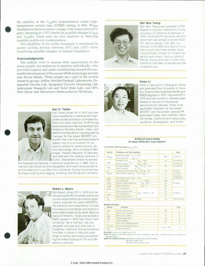
the stability of the VGS(th) characteristics under high- temperature reverse bias (HTRB) testing at 80% BVDSS (breakdown drain-to-source voltage with source shorted to gate). Stressing at 175°C checks for possible changes in IDss and VGS(th). These tests are very sensitive in detecting possible mobile-ion contamination.
The reliability of the solder die-attach is monitored by power cycling devices between 30°C and 130°C while monitoring possible changes in thermal impedance.
Acknowledgments The authors wish to express their appreciation to the
many people, too numerous to mention individually, who provided support and made contributions toward the suc cessful development of the power MOS-technology process and device family. These people are a part of the several research groups within Hewlett-Packard Laboratories (In tegrated Circuits Lab, Integrated Circuits Processing Lab, Instrument Research Lab and Solid State Lab), and HP's New Jersey and Microwave Semiconductor Divisions.
Karl H. Tiefert Kar l T iefer t jo ined HP in 1972 wi th pre v ious exper ience in working wi th h igh- power diodes and sil icon-controlled rec-
, t i f iers and beam-lead ICs. At HP he has | done process and device development I re lated to Schottky barr ier , noise, and | detectord iodesand is now engineer ing ! manager for the power MOSFET pro- I duct ion l ine. Karl has authored several
papers and is a co- inventor for s ix pa ten ts re la ted to semiconduc to r de vice technology. He is a native of SÃ c- k ingen, Federa l Republ ic o f Germany
r and a t tended the Ins t i tu te Juventus in l | Zur ich , Swi tzer land where he earned
the Engineer ing Dip loma in e lect r ica l engineer ing in 1963. Kar l is married, has one son and two daughters, and lives in a house that he and his wife built in Los Altos Hil ls, California. During his leisure time he enjoys soar ing and jogging, c l imbing, and ski ing wi th h is fami ly.
Robert L. Myers Bob Mye rs j o i ned HP i n 1978 and de veloped GaAs FET amplif iers before his current responsibi l i ty as a senior appl i cat ions engineer for power MOSFETs. His previous work exper ience inc ludes microwave circuit design and work on a solid-state phased-array radar. Bob is a nat ive of Amari l lo , Texas and earned a BSEE degree in 1970 f rom Texas Tech Univers i ty . He is marr ied, has one daughter and one son, and l i ves in Cupertino, Cali fornia. During his leisure t ime Bob is act ive in r i f le and p is to l t a rge t shoo t ing and en joys woodwork ing (he makes replicas of 1 7th and 1 8th century furniture).
Dah Wen Tsang Dah Wen Tsang was awarded a PhD degree in quantum e lec t ron ics by the Universi ty of Cal i fornia at Berkeley in 1978. He joined HP that same year and s ince then has worked on power MOS FET dev ice des ign. Dah Wen is a member of the IEEE and Sigma Xi and has co-authored three papers about us ing Schot tky d iodes fo r in f ra red de tectors and mixers. He is a nat ive of Peking, China and l ives in Union Ci ty , Cali fornia. Dah Wen is married and has a newborn son.
Victor LI Victor L i was born in Shanghai , China and a t tended R ice Un ivers i t y in Hous ton, Texas where he earned the BA and MSEE degrees in 1972. He joined HPin 1973 and has worked in several areas re la ted to the use of microwave semiconductor dev ices. V ic tor is an appl icat ion engineer for the power MOSFET and has wr i t ten several HP application notes. He is married, lives in Sunnyva le , Ca l i fo rn ia and en joys p lay ing tenn is , photography, and music .
S P E C I F I C A T I O N S H P M o d e l H P W R - 6 5 0 1 P o w e r M O S F E T
E L E C T R I C A L S P E C I F I C A T I O N S ( T c a s e , 2 5 - C )
M A X I M U M R A T I N G S :
P A C K A G E : C o n l o r m s t o J E D E C o u t l i n e T O - 3 P R I C E I N U . S . A . : H P W R - 6 9 0 0 D e s i g n e r s K i l ( t w o H P W R - 6 5 0 1 S . d a t a s h e e t , c a p a b i l i t y b r o c h u r e , a n d a p p l i c a t i o n s
l i t e ra ture ) . $46 .50 . M A N U F A C T U R I N G D I V I S I O N : M I C R O W A V E S E M I C O N D U C T O R D I V I S I O N
3 5 0 W e s t T r i m b l e R o a d S a n J o s e . C a l i f o r n i a 9 5 1 3 1 U . S . A .
A U G U S T 1 9 8 1 H E W L E T T - P A C K A R D J O U R N A L 2 3
© Copr. 1949-1998 Hewlett-Packard Co.

MOSFET Fabrication Requires Special Care
The h igh ga te dens i t y and the la rge a rea o f a ve r t i ca l power MOSFET cause the fabr icat ion y ie ld to be sensi t ive to contamina t ion and p rocess ing p rob lems s im i la r to those in MOS LSI man u fac tu r i ng . The key p rob lems tha t can p reven t t he p roduc t i on o f h igh-qua l i ty p roducts w i th adequate y ie lds are : 1 . Sod ium con tamina t ion (Na+) 2 . Par t i c le contaminat ion 3 . Process s tep i r regu lar i t ies , and 4 . Pho tomask ing de fec ts .
T o e l i m i n a t e t h e s e p r o b l e m s r e q u i r e s m a n u f a c t u r i n g I n a n u l t ra-c lean semiconductor fac i l i ty (F ig. 1) .
T o a v o i d N a + c o n t a m i n a t i o n , a l l c h e m i c a l s u s e d d u r i n g t h e manufactur ing process have especia l ly low Na+ content and the p r o c e s s p r o c e d u r e s a r e d e s i g n e d a n d e x e c u t e d t o k e e p N a + con tamina t i on l eve l s as l ow as poss ib le . Th i s i s necessa ry be cause the gate threshold voltage VGS(th) is extremely sensit ive to a n y s o d i u m c o n t a m i n a t i o n t h a t r e a c h e s t h e g a t e r e g i o n . O n e grain ( i f table salt (NaCI), for instance, contains enough sodium (if evenly distr ibuted) to contaminate devices on more than 250,000 t h r e e - l n c h - d i a m e t e r w a f e r s t o t h e p o i n t w h e r e V G S ( t h ) s h i f t s greater than 1.0V occur .
To assure long-term device rel iabi l i ty, especial ly the stabi l i ty of the thresho ld vo l tage, the dev ices are pass lva ted wi th a s i l i con n i t r ide layer , an excel lent barr ier against Na+ contaminat ion.
To e l im ina te pa r t i c le con tamina t ion a l l wa fe r hand l ing i s pe r
formed under c lean, laminar a i r f low condi t ions. To mainta in the necessary low par t i c le dens i ty ( less than 350 par t l c les /m3) a l l fabr icat ion area personnel conform wi th a s t r ic t dress code that requ i res tha t ha i r , hands , c lo th ing and shoes be covered w i th c lean, part ic le- f ree protect ive c loth ing (Fig. 1) .
To address the p rob lems o f p rocess i r regu la r i t i es ex tens ive use i s made o f compu te r - con t ro l l ed equ ipmen t . A mas te r com pu te r w i t h a se r i es o f t e rm ina l s a l l ows cons tan t access to a l l process specif icat ions. This system, cal led PCS (Process Control System), was developed by Hewlet t -Packard Laborator ies.1 PCS is a lso used for t racking lots and provid ing y ie ld and run h istory In fo rmat ion . A l l h igh- tempera ture processes , such as d i f fus ion and low-pressure chemica l vapor depos i t i on (LPCVD) , a re ca r r ied out in computer -cont ro l led fu rnaces (F ig . 1c) . Th is cont ro l covers not only temperature, gas f lows, and push-and-pul l rates, but also the proper sequence of Indiv idual process steps. Photo- mask ing defects are min imized by the use of h igh-qual i ty photo res is t , so lven ts and masks in an espec ia l l y l ow-par t i c le -coun t env i ronment . The pho tomask lng i s a lso done w i th a compute r - c o n t r o l l e d s y s t e m t h a t d i s p e n s e s a n d s p i n s o n p h o t o r e s i s t , softbakes, develops, r inses, and hardbakes wafers automatical ly. A p r o j e c t i o n m a s k a l i g n e r f o r a l i g n m e n t a n d e x p o s u r e o f t h e var ious layer pat terns Is an Integral part of th is system. Reference 1. C. Journal, "A Process Control Network," Hewlett-Packard Journal, June 1981.
Fig. (b) . etching Planar magnetron system used for metal deposition, (b) One of the wafer etching and c lean ing benches , (c ) Load ing wafe rs in to low-pressure chemica l -vapor -depos i t ion (LPCVD)
system.
2 4 H E W L E T T - P A C K A R D J O U R N A L A U G U S T 1 9 8 1
© Copr. 1949-1998 Hewlett-Packard Co.

Power Line Disturbances and Their Ef fect on Computer Des ign and Per formance Noise induced on the ac power l ine by machinery, l ightning, and even app l iances can be de te r imenta l to compute r per formance. By becoming fami l ia r w i th the nature o f the noise and i ts causes, the designer and user can take steps to min imize the ef fect on computers.
by Arthur W. Duel l and W. V incent Roland
ONE OF THE EARLIEST and continuing problems with computer systems is ac power line distur bances on customer premises. The computer manu
facturer is becoming increasingly concerned about the ac line transient and grounding environment that a com puter system is subjected to at a customer site. Design ing for immunity to power disturbances becomes pro hibitively expensive if all of the conceivable power con figurations and electrical noise sources are considered. For example, a forty-year-old house converted to office suites will probably not have third-wire grounding be cause that type of wiring was not required when the house was built. This particular situation is a problem because adequate grounding within and for a computer system is an integral part of the system design and must be considered for any computer installation.
If ac power line disturbances are not considered in the basic design or as part of the customer installation, the effects of a power anomaly may appear in many forms. The equipment may cease to operate, errors may occur in nor mal processing cycles or be introduced into data files and programs, or hardware damage may occur. A 10- millisecond power failure affects a period of time during which 10,000 computer operations may be performed.
The resolution of problems caused by ac power distur bances requires characterization of the ac power source and determination of the computer system's sensitivity to such anomalies. The effect of any possible solution on the man ufacturer and the customer must be evaluated. If the man ufacturer incorporates devices to protect the computer against all of the possible ac disturbances the initial cost of the computer increases significantly. A dilemma arises if, to keep purchase costs low, this is not done. In the purchase of any computer system, the cost of ownership must also be considered. The customer wants and should expect maximum use with a minimum of maintenance and downtime. If the computer is unable to handle power anom alies, the downtime and maintenance can become excessive and the cost of ownership increases dramatically.
Therefore, some compromise is required to minimize the overall cost to the customer. The customer should help by improving the environment for the computer system instal lation. The manufacturer should correctly and economi cally specify the environment required and educate the
customer about this specification in addition to incorporat ing economical design features that improve the computer system's resistance to ac power line disturbances.
Character izat ion of Power Sources Improving the immunity of a computer system to electri
cal noise requires adequate characterization of the ac power source. The terms frequently used to describe power line anomalies are discussed in the box on page 27. The noise
Lighting
Building Steel — •
Grounding •« — Bus
Motors
(a)
Building Steel —
Lighting
- Earth Ground
Computer Computer
Earth Ground
Fig. 1 . The grounding within a building can consist of both (a) s ing le-po in t (used fo r l igh t ing , motors , and app l iances) and (b ) mu l t i po in t (used fo r compute r sys tems) g round bus sys tems.
AUGUST 1981 HEWLETT-PACKARD JOURNAL 25
© Copr. 1949-1998 Hewlett-Packard Co.
present on an ac line can be generated by conditions unique to the customer's environment and by variations typically found on any power line supplied by a public utility. Wir ing codes developed by regulatory agencies to insure the safety of the user are often in conflict with line configura tions designed for noise reduction.
Computer manufacturers and users cannot influence or change these facts significantly. To place these conditions in proper perspective, computer systems and other sensi tive control loads represent less than 0.01% of the total utility load. Consequently, it is understandable that a utility will not try to prevent power disturbances affecting com puters. Wiring codes are also generated with respect to the general consumer. Generally wire sizes and grounding specifications are based on electrical loads associated with major appliances and heavy electrical machinery, and do not take into consideration the low impedances that are required when computer systems are switching at milli second speeds.
Factors describing the quality of an ac power line are nominal line voltage, service voltage, utilization voltage, statistical distribution of transients generated by the utility and the customers, and regulatory body specifications. In the U.S.A. there are national standards developed by American National Standards Institute (ANSI), and these specifications are typically used by U.S. utilities to permit better networking and interchange of power.
Nominal line voltage is the level close to the average value expected during normal operation. This value, mea sured at the outlet, varies with geographic location.
The most important parameter that the utility must adhere to is the service voltage — the voltage supplied to the customer's meter. In the San Francisco Bay area it is 114 volts minimum to 126 volts maximum. For three-phase- wye distribution, it is 197 volts minimum to 218 volts maximum. Generally speaking , the three-phase line voltage will be lower than the nominal 208 volts, but the power company is still within specifications as long as the line voltage does not go below the minimum service voltage.
The utilization voltage (at the wall outlet) is 110 volts minimum to 125 volts maximum. For three-phase-wye dis tribution, it is 191 volts minimum to 216 volts maximum. Herein lies a difficulty. The building owner is responsible for all internal wiring within the building from the meter to the wall outlet. Therefore, if there is a problem with the voltage, it is of little value to a user to have the power company measure voltage at the wall outlet because they have no control over the internal wiring of a building.
To compound the problem, there are some studies being made by U.S. utilities to change generating voltages to conserve energy. The federal government is strongly suggesting to the utilities that there be a conservation volt age reduction. This is a systematic lowering of distribution voltages to reduce energy consumption by customers. The minimum service voltage would remain the same but the maximum would be lowered. Suggested ranges would be either 114 to 1 18 volts or 114 to 120 volts. When the generat ing margin narrows, the utilities are forced to do more load switching. The result is more transients.
It is impossible to quantize transients caused by utilities switching loads during peak demand hours, or by breaker
action during some fault condition. A model can be de veloped, but it is a function of such parameters as line impedance, circuit breaker size, fault current, and other widely varying factors. Obviously, the computer installer and customer should be fully aware of possible problems when the computer system is installed near a utility substa tion or switchyard.
Customer Site Characteristics Noise on the power line can be generated in many differ
ent ways at the computer user's site. Electric clock systems signal-modulate the power distribution within a facility once an hour to update all electric clocks. Flicker (momen tary voltage dip due to the starting of a large appliance) can occur typically 10 times per hour and the duration can be from 160 to 670 ms. The maximum amplitude of a transient is directly proportional to the velocity with which a contact opens, and is independent of power consumption. A 400-hp motor (with large slow-moving contacts) produces transients with one-tenth the amplitude of those produced by an electric clock motor. Fluorescent light switching can cause an extended transient of 2-MHz, 500V oscillations lasting for 20 /us. Power characteristics of an installation change with time even though good site preparation is done initially. Vending or copy machines can be added inadver tently to circuits and grounding that were initially wired exclusively for computer systems.
The most common customer problems associated with ac power are nonisolated grounds and improper conductor sizes. These occur even when the grounding and wiring are done according to code.
Two categories of ground systems must be considered: 1. Safety (dc conduction) — the electrical power grounding
system which includes all ac power, distribution and utility service power used for lighting, equipment power, et cetera.
2. EMI (RF conduction) — signal circuit grounding which includes all electronic and electrical control circuits
Sub-Panel Ground Neutral
LG= Logic Ground
F i g . 2 . V o l t a g e d i f f e r e n c e s b e t w e e n t h e l o g i c g r o u n d s o f i n t e r c o n n e c t e d c o m p u t e r u n i t s c a n e x i s t i f g r o u n d i m p e d ances and power needs di f fer between any two uni ts .
2 6 H E W L E T T - P A C K A R D J O U R N A L A U G U S T 1 9 8 1
© Copr. 1949-1998 Hewlett-Packard Co.
Definitions: ac Power Anomalies
Power l ine d is turbances may be c lass i f ied in to severa l types (see Fig. 1): Vo l tage va r ia t i on : The supp l i ed vo l tage dev ia tes f rom the p re scr ibed input range. Input be low the range is a sag, above is a surge. Sags can be caused by del iberate ut i l i ty cutbacks (brown outs) to lower power consumpt ion, by customer loads for which the ut i l i ty cannot compensate, or by an excessive inrush start ing current to powered-up equipment. Surges originate from uti l i ty l ine ma l func t ions o r sudden changes in power demand ( remova l o f heavy loads) which cannot be corrected instantaneously.
Line-to-Line or Line-to-Neutral Voltage
- / T - 7 - -
(a)
- - ^ - - V - V -
Normal Sag Normal Surge Power Fail
v v v v w v v v Normal
Frequency Low
Frequency Normal
Frequency (b)
A A A A ^ A A A A v v v v v v v
Common ( c ) M o d e
Normal Mode
Fig . 1 . Graph o f the ac l i ne vo l tage under (a ) norma l , sag , su rge , and powe r fa i l cond i t i ons , ( b ) no rma l and abno rma l f r e q u e n c y c o n d i t i o n s , a n d ( c ) w i t h c o m m o n - m o d e a n d normal-mode transients.
Frequency va r i a t i on : The f requency o f t he power l i ne vo l t age dev ia tes f rom the p resc r ibed i npu t range . Sudden changes i n load to the uti l i ty, switching of power between uti l i ty companies, or generator mal funct ion can cause such var ia t ions. Powerfail: Total removal of the input voltage to the computer for at
Amplitude
50%
10%-
Rise T ime- D u r a t i o n | -
Fig. 2. Characterist ics of transient noise on an ac power l ine.
least 5 of Switching of power by ut i l i t ies, either for the purpose of r e d i s t r i b u t i n g l o a d s o r c o r r e c t i n g s h o r t c i r c u i t s , w i l l p r o d u c e p o w e r f a i l u r e s f r o m a f e w c y c l e s t o s e v e r a l s e c o n d s . P o w e r equipment fa i lure can resul t in outages of minutes to hours. T r a n s i e n t : A d i s t u r b a n c e o f l e s s t h a n 5 m s d u r a t i o n . T h e ampl i tude, r ise t ime, durat ion, resu l tant osc i l la t ion ( i f any) and repeti t ion rate (see Fig. 2) determine the effect on the computer's operat ion. We can classify transients into three types, dist inguish ing them by the i r sources.
Transients from nearby sources (within 50 feet of the computer) have very fas t r i se t imes (nanoseconds) r ich in h igh- f requency conten t . The power cord becomes a t ransmiss ion l ine , and the propagat ion o f the t rans ient is in f luenced by d is tance, condui t , a d j a c e n t c o n d u c t o r s ( i n t o w h i c h t h e s e t r a n s i e n t s m a y b e coupled) , f la tness o f the cord aga ins t the f loor , and socket con nect ions . Because o f h igh- f requency coup l ing between the con ductors in the cord, these t rans ients are usual ly common-mode b y t h e t i m e t h e y r e a c h t h e c o m p u t e r . S o u r c e s o f t h i s t y p e o f t ransient are anything with mechanical breaker contacts, such as cof fee pots , e lect r ic typewr i ters , and c lock motors.
Trans ients produced by d is tant sources w i l l have s lower r ise t imes (mic roseconds) and longer dura t ions than the f i r s t t ype . T h e y a r e g e n e r a t e d b y a n y e l e c t r i c a l d e v i c e t h a t p r o d u c e s e n o u g h t r a n s i e n t e n e r g y t o p r o p a g a t e t h r o u g h t h e d e v i c e ' s c i rcu i t breaker and d is t r ibut ion panel back to the c i rcu i t breaker f e e d i n g t h e c o m p u t e r . E l e v a t o r m o t o r s , i n d u s t r i a l m a c h i n e r y (either on the premises or a block away), and air condit ioners are p o s s i b l e s o u r c e s . T h e s e t r a n s i e n t s a r e n o r m a l - m o d e o r common-mode.
Other transients with rise times similar to those of distant-source t rans ients and wi th a common-mode s t ruc ture can be produced by ut i l i ty d is t r ibut ion faul ts and resul tant arc ing, or by l ightn ing, d i rect or induced, on the ut i l i ty power po le.
associated with a computer system. In the first category, all neutral and ground line distribu tions are wired on separate buses and connected together at the main power transformer entrance to the building, mak ing a single-point ground.1 In the second category, the ground from the electronic equipment is connected to the nearest steel structural beam to make a multipoint ground (see Fig. 1) from a facility viewpoint.
Because computer systems typically use earth ground as a reference within each cabinet and the entire system is
connected to the facility earth ground, it is very important that the computer system be connected to an EMI ground ing system. Fig. 2 shows the system power and interface cable hookups and points where common-mode noise (voltage between both lines and ground) can exist. The net voltage difference between any two points on the ground network usually will be small (1 to 3 volts). However, the current through certain network paths can be on the order of 3 to 5 amperes with occasional currents of 10 to 15 amperes.
For typical building wiring, electricians use water pipes
AUGUST 1981 HEWLETT-PACKARD JOURNAL 27
© Copr. 1949-1998 Hewlett-Packard Co.

and conduit as ground. For safety and minimal shock hazard, this is legal from an electrical code viewpoint. For EMI suppression it is inadequate because lighting loads, vending machines, and other types of office equipment are connected to the same grounding system. Another common contributor to stray ground currents within a facility is the connection of the ac neutral line to earth ground inside the branch panel. Then the ground network becomes a part of the ac return line to the main building service entrance. The line current will divide between the neutral line and the ground return network in inverse proportion to the imped ance of the two paths.
Because instantaneous power surges are required by a computer system during turn-on and normal operation, wire sizes must be large enough to keep the voltage from sagging. For example, during computer turn-on, switching power supplies can require currents peaking at 150 A and decaying exponentially to 2 0 A in less than 30 ms . If the wire size is inadequate, the input voltage can sag below the required input voltage tolerance of the computer for a period of 100 ms, causing the power-control circuitry to detect a powerfail, thus shutting the system off. Wire sizes specified by typical code requirements are usually at least one size smaller than required for computers. Such code requirements make it difficult for the computer manufac turer to convince the customer and electrician that larger wire sizes must be used if the computer system is to operate satisfactorily.
Computer System Sensi t iv i ty Circuits used in a modern computer system are extremely
fast and more vulnerable to noise than circuits used a few years ago. Because there is the same high-frequency sen sitivity in a peripheral as in the mainframe, the same design parameters are used to immunize the total system from outside disturbances. For software, data integrity is pro tected from power line transients by using various error correction codes (ECC) in the transmittal of data between parts of a system, and "disc retrys" are used on disc drives when errors occur. Therefore, power line noise can be masked by using software error-correction techniques.
To achieve less susceptibility to power line noise, larger systems (costing more than $200,000) often use motor- generator sets for the power sources. These sets are pur chased as part of the system, and can provide a near-perfect power source. Small computers containing the same type of internal circuitry are subjected to the same types of power disturbances as the larger computer systems, but instead use ac input filter design or components such as metal- oxide-varistors (MOV) to improve noise immunity.
Impact on Customer and Manufacturer Making positive determination that a computer installa
tion problem is caused by power line disturbances can be very difficult. The occurrence may be random, and the effects on the system may be different depending on the state of the electronics at the precise time of the disturbance. Symptoms of such problems overlap with those that may be caused by intermittent electrical connections, electrostatic discharge (BSD) either directly to the computer or indi rectly via other objects in the immediate vicinity, or even
software program bugs. If intermittent ac disturbances are suspected, isolating them may require expensive monitor ing equipment that is installed for a period long enough to detect the next occurrence.
The time required to analyze and repair an ac line distur bance problem can be several times the hours required for analysis and repair of other service problems. During the process of diagnosis machine time is lost and the service engineer may have to visit a site several times before proper remedies can be made. In the case of ac power transients, which can be random and are unpredictable, direct correla tion of cause and effect is extremely difficult to obtain.
Detect ion of a Noise Problem On-Si te The service engineer's objective is to prevent power line
disturbances from reaching the computer by discerning their characteristics, and then either remove the source or isolate the computer from the source. A comprehensive set of site preparation guidelines is sent to the customer prior to delivery of a computer system. If the guidelines are fol lowed, the likelihood of power line disturbance problems is minimized. The service engineer may participate in site preparation with the customer. Whether during a site prep aration or installation, or in troubleshooting an installed system, a service engineer may proceed through the follow ing steps: ú Look outside the customer's site. Check for major indus
tries in the area that consume large amounts of electric ity. Their operation can cause voltage variations or tran sients to be propagated to other users sharing the same output of the utility company's substation transformer.
• Look within the customer's site for heavy electrical equipment. A transient source within the site may affect
Noise Removed f rom ac L ine
G N L
Noise Coupled to CPU
Noise Coupled to I /O Cable
Printer ^ C h a s s i s
Noise Coupled to Chassis
Fig. 3 . A l l un i ts in a computer system must be iso la ted f rom the ac power l ine . Otherwise, an un iso la ted un i t , the pr in ter shown he re , can coup le no ise to an i so la ted un i t , t he CPU here, v ia the I /O interconnect ions.
2 8 H E W L E T T - P A C K A R D J O U R N A L A U G U S T 1 9 8 1
© Copr. 1949-1998 Hewlett-Packard Co.
the computer installation more severely than a distant source because nearby transients, especially fast-rise-time pulses, do not dissipate significantly in the short dis tance before they reach the computer. Note local weather conditions. Electrical storms may cause transients by direct lightning hits on utility lines or induced coupling through nearby earth strikes. Besides the transients, the utility company's hardware is some times affected, causing voltage variations or powerfails. Check the wiring from the building's utility power con nection to the outlets in the computer room. Feedback from HP's systems specialists in the field indicates that improper site wiring is often the major cause of power line disturbance problems. With the help of an electri cian who is aware of local codes, check the building's electrical layout, and look for load distributions that overload any circuits, or branch circuits that allow other electrical devices to use the same circuit breaker as the computer. Distribution and breaker panels must have solid electrical connections, and breakers and wire capacities must equal or exceed the computer's demand. Check equipment layout at the computer installation. All
devices must be plugged into their own wall outlets. Extension cords with multiple outlet boxes must not be used. If possible, avoid extension cords altogether. Check especially for grounding of all devices by having the electrician confirm that the ground wire is continuous back to the building's service entrance. A computer sys tem can pollute its own power if these procedures are not observed. Up to this point all checks have been visual. If no answers
are obvious, measurement equipment is required. Tools for analyzing ac power become progressively more compli cated and expensive as the problem becomes more difficult. First, wall outlets can be checked for proper polarity of the lines and ground, and for existence of ground by a receptacle-circuit tester. At the same time, a ground loop impedance tester (GLIT) can be used to test the integrity between the neutral line and ground. However, it only checks impedance at the line frequency, not at high fre quency or RF.
When intermittents occur, the cost of the tool goes up significantly and requires the user to have some skill and training in its operation. Such a tool is a power line monitor
Table I Features of ac Line Protect ion Devices
Device Description Voltage Variat ion Protection
Shielded isolation A transformer with Input/output ratio t ransformer isolated, electro- can be manually
statically shielded primary and sec ondary windings.
Frequency Variation
Protection None
Power fa i l P ro tec t i on
None
Normal -Mode Transient Protection
Common-Mode Transient Protection
selected by jump ering windings.
Tap-switching A shielded isola- Good. For a broad None None
Low. Transformer High. 120 dB CMR windings may specifications are limit bandwidth, available, but pulses get through.
Low to medium. High. 120 dB CMR
AUGUST 1981 HEWLETT-PACKARD JOURNAL 29
© Copr. 1949-1998 Hewlett-Packard Co.

which can be left at a customer site for several days and will measure and record voltage surges, sags, frequency varia tion, powerfails, and transients. Measurements are logged on a printout with their times of occurrence.
Throughout the measurement process, the service en gineer notes the nature of the disturbance and checks it against factory-supplied specifications for the computer.
After these checks are completed, a solution is likely to be evident. It may be one of two types: 1) the problem source is identified and can be removed, or 2) the source cannot be removed or cannot be identified, but the nature of the dis turbance has been characterized and a device to isolate the computer can be specified.
Isolat ion Devices Isolation devices are available with a variety of features to
match the needs of the problem site. Manufacturers offer product lines with varying degrees of protection and power handling capabilities. A qualitative summary of features is given in Table II.
Isolation devices must be installed with full knowledge of their capabilities in mind. Large computer sites set up through subcontractors place no burden of installation (other than financial) on the customer. Customers doing their own installation, however, must work with the service engineer to fulfill the prerequisites before successful opera tion can happen. Isolation transformers and line condition ers, in particular, are not panaceas that are merely uncrated and connected between the computer and the wall outlet. These devices have their own input and output specifica tions that must be met, or else a new set of problems will emerge to replace the old ones. All devices in the computer system should be isolated. Otherwise, as shown in Fig. 3, an unprotected system component can receive a transient on its ac input and couple the noise to its chassis. Then the noise is coupled to an I/O cable leading to the chassis of the "protected" component.
I /O Cables-, Computer Componentsx
Standard ac P o w e r C o r d s
High-Voltage F a c t o r y L o w - I n d u c t a n c e M a i n s C o u p l i n g C a p a c i t o r s
Output for Monitoring
Devices at Load
L ine Impedance Stabi l izat ion Network
Coupling Box
Fig . 4 . Equ ipment sens i t iv i ty to t rans ients can be eva luated by in jec t ing pu lses onto the power l ines us ing the s impl i f ied tes t a r rangement shown above.
Factory Act ion to Minimize Susceptibi l i ty The key factor in effective factory design and testing for
ac disturbance immunity is realistic simulation. Underde- sign will result in dissatisfied customers and high warranty costs, while overdesign may inflate the manufacturing cost (and thus selling price) with no perceived increase in per formance. Objective data on the nature of disturbances is scarce. HP's test procedures have been developed based upon published data " and feedback from service en gineers. Test specifications at HP's Business Computer Group fall into four categories:
Input voltage test. Using a variable transformer, the de vice is tested over a prescribed tolerance about a pre scribed design center, or nominal value. Most of the computers have nominal input values of 100, 120, 220, and 240 volts ac rms. The tolerance about each of these values is +5%, -10%. Input frequency test. A solid-state power amplifier whose output tracks the frequency of a variable oscillator supplies power to the tested device. Computer equip ment electronics generally has little difficulty in meeting a specification of 47.5 to 66 Hz. Devices with ac syn chronous motors, or terminals with a fixed CRT sweep rate, will experience problems if the frequency varies more than 1 Hz from the design center.
• Powerfail test. The computer is tested for reactions to momentary removals of power. For test repeatability, semiconductor devices in series with the ac line are used to interrupt the power under control of an electronic timing generator. Durations of less than one cycle (20 ms) should have no effect on operation of the product. Greater durations may initiate an automatic shutdown proce dure. An absolute rule is that no data be lost. In the case of computer semiconductor memory, batteries provide backup power for at least 15 minutes. Flying-head disc units retract their heads before shutting down.
Real-world powerfails can be of any duration, and the power supply hardware must be able to respond properly to restoration of power at any time during its power- down sequence. Otherwise, the supplies and their con trol logic may hang in a shutdown state, requiring a second removal of power (for a longer duration) to clear the condition. Further, a powerfail event may occur in the midst of a low-line-voltage condition near the bottom of the specified operating range. This combination must not affect recovery performance.
-.-. Line transient tests — Pulse generators are used to inject energy into the ac line input. A test arrangement is shown in Fig. 4. More than for any other power disturbance test, the choice of specifications for this test is difficult to substantiate. Although the numeric parameters used by HP are proprietary, the general test procedure is: 1. Apply the following types of transients: high-speed
common-mode, slow-rise-time normal-mode, and slow-rise-time common-mode.
2. Apply pulses of positive and negative polarity, and vary pulse timing relative to the phase of the ac wave.
3. Gradually increase amplitude of the applied pulse until a failure occurs, or the test specification limit is met.
4. During the test, the system runs programs that exten-
3 0 H E W L E T T - P A C K A R D J O U R N A L A U G U S T 1 9 8 1
© Copr. 1949-1998 Hewlett-Packard Co.

Shielded ac Power Fi l ter and Power Supply Area
Low-Pass Impedance Connection
Floor
F i g . 5 . T w o g r o u n d i n g a p proaches can be used to increase i m m u n i t y t o l i n e t r a n s i e n t s , ( a ) C o m m o n s a f e t y a n d l o g i c g rounds . T rans i en t ene rgy i s un i formly d is t r ibuted throughout the chassis so that no noise potentials exist between the internal circuits, ( b ) I s o l a t e d s a f e t y a n d l o g i c g r o u n d s . T r a n s i e n t e n e r g y i s t ight ly coupled to the chassis, but t he i n te rna l c i r cu i t s a re i so la ted w i t h r espec t t o t he chass i s by a low-pass f i l ter.
sively exercise the hardware and report errors the moment they occur.
A similar procedure is used in the evaluation of isolation devices or shielded ac power cords and I/O cables. In all cases of factory testing, once the operating limit of the system is found, measurements are logged for reference in case consultation with the field is necessary.
Future Trends Computer manufacturers must prepare themselves for
two evolving challenges from ac power line disturbances. First, commercial power from the utility companies is going to become less stable and reliable than at present. This is not by design of the utilities, but a consequence of rising customer demand that outpaces the growth of the utilities' capability. As the unused power margin of the utilities dwindles, rotating blackouts and brownouts may be used, and power will be borrowed from other regions. Second, the shrinking prices of computer technology will bring it within the realm of users who cannot afford, and do not care to understand, electrical site preparation for their computers. The tendency of designers to achieve lower cost by lowering ac power performance expectations and as sociated hardware costs must be resisted. In fact, an increas ing percentage of new project investment must be addressed to this issue. Future computer system designs must also consider the increasing susceptibility of internal compo nents to transients because of their higher operating fre quencies. The use of undedicated wall outlet power, which implies sharing power with other office appliances, must be considered because of the increasing portability of comput ers and peripherals.
One approach to achieving transient immunity requires meticulous care in the design of front-end filters for each component in the system. If the filters are to be effective, the grounding and ground reference within a cabinet must be free of electrical noise so that the filters will have a low- impedance plane for discharging unwanted transients. Fundamental to the design of computer systems is the elimination of ground loops between peripherals and the computer. The present use of single-point grounding (iso lated ground) for the total system is a brute force method. Product designers can choose from two alternative ground ing approaches to maximize immunity to line transients. The first approach bonds chassis and logic grounds to gether at many physical points. Any transient signals enter ing the system are thus coupled to both grounds simultane ously. The product's entire contents momentarily rise in potential relative to its surroundings (see Fig. 5a), although within the product no noise potentials will exist. When such products are connected via I/O cables, problems may result. Unequal coupling of transient energy to the cabinets can create a potential across the logic grounds of the cable transceivers which may cause incorrect data transmission.
The second approach requires total separation of the cabinet safety ground and logic ground except for one con nection through a low-pass filter (Fig. 5b). All incoming transients are coupled to the chassis frame by the input filters as before, but they do not couple to logic ground (except by radiation). Circuits therefore remain quiet with respect to other devices that may be connected by cables, although the chassis frame may momentarily have a poten tial. Double-shielded cables may be necessary, with the outer shield connected to each chassis and the inner shield
AUGUST 1981 HEWLETT-PACKARD JOURNAL 31
© Copr. 1949-1998 Hewlett-Packard Co.
connected to logic ground. This technique requires that all devices in the system follow the same scheme.
Other system design techniques are: High-frequency power distribution to I/O devices. Hewlett-Packard has implemented this design in the HP 1000 L-Series Computers. A 25-kHz single-phase power distribution system is transmitted to various remote com ponents of the total computer system. The high-frequency ac power is converted to dc power at the remote device to reduce ground noise coupling between the central processing unit (CPU) and sensitive I/O devices. Optical isolators at each end of a wire cable to reduce or eliminate common-mode noise between system compo nents. Thus, the signal returns are returned to the source of the signal instead of being connected with the ground at the receiving end. Optical interfaces can pass dc as well as pulse-type signals (this technique is used to con nect terminals to the HP 250 computers). Fiber optic cables can be used instead of wires to form a wholly optical interface between system components.
Acknowledgments We would like to express our thanks to Jim Gillette at the
Data Systems Division, whose detailed research and sum marizing of various papers, including the references listed below, originated new thoughts on test and specification procedures. Larry Rea, formerly of the Customer Engineer Organization, provided valuable inputs based upon experi ence with solving customer problems, and Jim Brannan in our reliability group has been instrumental in building the customized system-level test tools. Norm Marschke, Com puter Systems Division, has made significant contributions in design of system noise immunity and power-control circuits for new HP products.
References 1. H. Denny and J. Moody, "Considerations in the Design of a Grounding System for a Complex Electronic Facility," IEEE Electromagnetic Compatibility Symposium Record, July 1974, pp. 85-91. 2. J. Hull and W. Wethercot, "The Frequency of Occurrence and the Magnitude of Short Duration Transients in Low-Voltage Sup ply Mains," The Radio and Electronic Engineer, September 1964, pp. 185-190. 3. W. Hayter, "High Voltage Nanosecond Duration Power Line Transients," San Jose Testing Laboratory, International Business Machine Corp, Technical Report S-1117, November 13, 1964.
4. F. and and G. Hann, "Surge Voltages in Residential and Industrial Power Circuits," IEEE Transactions on Power Apparatus and Systems, July/August 1970, pp. 1049-1056. 5. "World Electricity Supplies," British Standards Institute, 1974. {Through Technical Export News, a service of the British Standards Institute.) 6. G. Allen and D. Segall, "Monitoring of Computer Installations for Power Line Disturbances," IBM Corporation, 1973 IEEE Power Engineering Society winter meeting, New York, New York, January 1974, Paper C 74 119-6.
W. Vincent Roland Vince Roland, a nat ive of Louisvi l le, Ken tucky , i s a g raduate o f the Un iver sity of Louisvil le, where he received the Master 's degree In e lect r ica l engineer ing in 1 973. He then joined HP and has worked In several of HP's d iv is ions. V ince Is now the product assurance hardware engineering manager at HP's Computer Systems Div is ion. He Is a member o f the IEEE, marr ied, and a resident of Sunnyvale, California. Vince is an act ive church member and enjoys pho tography , wh ich he does as a spare-t ime business.
Arthur W. Duel l Art Duel l came to HP in 1972, did tech n ica l wr i t ing and suppor t for the HP 2000 Computer, was a service engineer for the HP 300 Computer, and now is a serv ice engineer for the HP 250 Compute r . H is p rev ious work exper i ence was in circui t and system design. Ar t earned the BSEE degree in 1957 from the University of Colorado and has done graduate work at the University of Santa Clara, California. He is a member of the IEEE and co-hosts HP's computer systems group on ac power. A native of Windsor , Co lorado, he is marr ied and has two sons. Ar t Is an act ive church
member and en joys sk i ing and f i sh ing . He and h is w i fe a re busy remodel ing thei r 30-year-o ld home in Cupert ino, Cal i forn ia.
Hewle t t -Packard Company , 1501 Page Mi l l Road, Palo Al to , Cal i forn ia 94304
R D J Q U R N A L
Bulk Rate U.S. Postage
Paid Hewlet t -Packard
Company
AUGUST 1981 Vo lume :
Technica l In format ion f rom the Laborator ies of Hewlet t -Packard Company
Hewle t t -Packard Company , 1501 Page M i l l Road Palo Al to, Cal i forn ia 94304 U.S.A.
Hewle t t -Packard Cent ra l Ma i l ing Depar tment Van Heuven Goedhar t laan 121
1 181 KK Amste lveen. The Nether lands Yokogawa-Hewle t t -Packard L td . , Sug inami -Ku
Tokyo 168 Japan
C O D E - 3 L D b N 2 4 4 - 7 M O F F E T T F I E L D C A 9 4 0 3 5
/~ \ | | A K I ^^ I " "1 y*"^ [~~ A f~"N r~"N r^ I O ^^ . To change your address or de lete your name f rom our mai l ing l is t p lease send us your o ld address label . Send V > | l / A l N ( j t V ^ / l / A L J L J r i L L O O . c h a n g e s t o H e w l e t t - P a c k a r d J o u r n a l , 1 5 0 1 P a g e ' M i l l R o a d . P a l o A l t o , C a l i f o r n i a 9 4 3 0 4 U . S . A . A l l o w 6 0 d a y s .
© Copr. 1949-1998 Hewlett-Packard Co.