Embed Size (px)
Citation preview
198 IEEE TRANSACTIONS ON CIRCUITS AND SYSTEMS–I: REGULAR PAPERS, VOL. 65, NO. 1, JANUARY 2018
A Reconfigurable Streaming Deep ConvolutionalNeural Network Accelerator for Internet of Things
Li Du, Member, IEEE, Yuan Du, Member, IEEE, Yilei Li, Junjie Su, Yen-Cheng Kuan, Member, IEEE,Chun-Chen Liu, and Mau-Chung Frank Chang, Fellow, IEEE
Abstract— Convolutional neural network (CNN) offers signifi-cant accuracy in image detection. To implement image detectionusing CNN in the Internet of Things (IoT) devices, a streaminghardware accelerator is proposed. The proposed accelerator opti-mizes the energy efficiency by avoiding unnecessary data move-ment. With unique filter decomposition technique, the acceleratorcan support arbitrary convolution window size. In addition,max-pooling function can be computed in parallel with convo-lution by using separate pooling unit, thus achieving through-put improvement. A prototype accelerator was implemented inTSMC 65-nm technology with a core size of 5 mm2. Theaccelerator can support major CNNs and achieve 152GOPSpeak throughput and 434GOPS/W energy efficiency at 350 mW,making it a promising hardware accelerator for intelligentIoT devices.
Index Terms— Convolution neural network, deep learning,hardware accelerator, IoT.
I. INTRODUCTION
MACHINE Learning offers many innovative applica-tions in the IoT devices, such as face recognition,
smart security and object detection [1]–[3]. State-of-the-artmachine-learning computation mostly relies on the cloudservers [4], [5]. Benefiting from the graph processingunit (GPU)’s powerful computation ability, the cloud canprocess high throughput video data coming from the devicesand use CNN to achieve unprecedented accuracy on mostAI applications [6]. However, this approach has its owndrawbacks. Since the network connectivity is necessary forcloud-based AI applications, those applications cannot run inthe areas where there is no network coverage. In addition, datatransfer through network induces significant latency, which isnot acceptable for real-time AI applications such as security
Manuscript received December 8, 2016; revised June 4, 2017; acceptedJuly 27, 2017. Date of publication August 16, 2017; date of current ver-sion January 5, 2018. This paper was recommended by Associate EditorA. Sangiovanni Vincentelli. (Corresponding authors: Li Du; Yen-Cheng Kuan;Mau-Chung Frank Chang.)
L. Du, Y. Du, and C.-C. Liu are with the High Speed Electron-ics Laboratory, University of California at Los Angeles, Los Angeles,CA 90095 USA, and also with Kneron Inc., San Diego, CA 92121 USA(e-mail: [email protected]).
Y. Li is with the Novumind Inc., Santa Clara, CA 95054 USA.J. Su is with Kneron Inc., San Diego, CA 92121 USA.Y.-C. Kuan is with National Chiao Tung University, Hsinchu 30010,
Taiwan (e-mail: [email protected]).M.-C. F. Chang is with the High Speed Electronics Laboratory, Uni-
versity of California at Los Angeles, Los Angeles, CA 90095 USA, andalso with National Chiao Tung University, Hsinchu 30010, Taiwan (e-mail:[email protected]).
Color versions of one or more of the figures in this paper are availableonline at http://ieeexplore.ieee.org.
Digital Object Identifier 10.1109/TCSI.2017.2735490
system. Finally, most of the IoT applications have a toughpower and cost budget which could tolerate neither localGPU solutions nor transmitting massive amounts of image andaudio data to data center servers [7].
To address these challenges, a localized AI processingscheme is proposed. The localized AI processing scheme aimsat processing the acquired data at the client side and finishesthe whole AI computation without communication networkaccess. Conventionally, this is done through local GPU or DSP.However, this results in a limited computation ability andrelatively large power consumption, making it not suitable forrunning computation-hungry neural network such as CNN onpower limited IoT devices [8]. Consequently, it is crucial todesign a dedicated CNN accelerator inside the IoT devicesthat can support a high performance AI computation withminimal power consumption. Some of the reported works inthe neural network acceleration are focusing on providingan architecture for computing general neural network. Forexample, in [9], an efficient hardware architecture is proposedbased on the sparsity of the neural network through pruning thenetwork properly. However, it is a more general architectureto compute the fully-connected deep neural network withoutconsidering parameter reuse. On the contrary, the CNN has itsunique feature that the filters’ weights will be largely reusedthroughout each image during scanning. Benefiting fromthis feature, many dedicated CNN hardware accelerators arereported [10]–[12]. Most of reported CNN accelerators onlyfocus on accelerating the convolution part while ignoring theimplementation of the pooling function, which is a commonlayer in the CNN network. In [10], a CNN hardware accel-erator using a spatial architecture with 168 processing ele-ments is demonstrated. In [11], another dedicated convolutionaccelerator with loop-tiling optimization is reported. Sincepooling function is not implemented in those accelerators,the convolution results must be transferred to CPU/GPU torun pooling function and then fed back to the acceleratorto compute the next layer. This data movement not onlyconsumes much power but also limits overall performance.On the other hand, some works report highly configurableneural network processers but they require complicated dataflow control. This adds hardware overhead to IoT devices. Forexample, [12] reports a CNN processor occupying 16 mm2
silicon area in 65nm CMOS technology, which can be intol-erable for low-cost IoT chips. In addition, several recentreports, such as [13], proposed to use memristors to performneuromorphic computing for CNN. However, the fabrica-tion of memristors currently is still not supportive in major
1549-8328 © 2017 IEEE. Personal use is permitted, but republication/redistribution requires IEEE permission.See http://www.ieee.org/publications_standards/publications/rights/index.html for more information.
DU et al.: RECONFIGURABLE STREAMING DEEP CNN ACCELERATOR 199
CMOS foundries [14]. Thus this architecture is hard to embedinto the IoT chips.
In this study, we propose a new streaming hardware archi-tecture for CNN inference at the IoT platform and assume theCNN model is pre-trained. We focus on the optimization ofthe data-movement flow to minimize data access and achievehigh energy efficiency for computation. A new methodologyis also proposed to decompose large kernel-sized computationto many parallel small kernel-sized computations. Togetherwith the integrated pooling function, our proposed acceleratorarchitecture can support completed one-stop CNN accelerationwith both arbitrarily sized convolution and reconfigurablepooling. The main contribution of this paper includes:
1) A CNN accelerator design using streaming data flow toachieve optimal energy efficiency.
2) An interleaving architecture to enable parallel comput-ing for multiple output features without SRAM inputbandwidth increment.
3) A methodology to decompose large-sized filter computa-tion into many small-sized filter computation, achievinghigh reconfigurability without adding additional hard-ware penalty.
4) A supplementary pooling block that can support pool-ing function while the main engine serves for CNNcomputation.
5) A prototype design with FPGA verification, which canachieve a peak performance of 152 GOPS and energyefficiency of 434 GOPS/W.
The paper is organized as follows. In Section II, we firstintroduce the main layers composing CNNs. In Section III, weintroduce our system’s overview architecture. In Section IV,we discuss the proposed streaming architecture to achievehigh-efficiency convolution computation, filter decompositiontechnique to provide reconfigurability and pooling implemen-tation. Key modules’ design is explained in Section V. Finally,the experimental results are reported in Section VI and theconclusion is drawn in Section VII.
II. LAYER DESCRIPTION
The state-of-art CNN networks (e.g., AlexNet,VGG-18, etc.) [15]–[17] are mainly composed of three typicallayers: convolution layer, pooling layer and classificationlayer. Convolution layer composes the majority of the neuralnetwork, with pooling layer inserted between two convolutionlayers to achieve intermediate data size reduction and non-linear mapping. Classification layer is usually included as thelast layer of the CNN, which does not require a large amountof computation. Here, we assume that the classification layercan be realized through software computation and will not beimplemented in the hardware accelerator.
The following subsection will explain the convolution layerand the pooling layer’s functions in details.
A. Convolution Layer
The primary role of a convolution layer is to apply convo-lution function to map the input (previous) layer’s images tothe next layer.
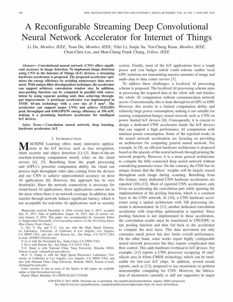
Fig. 1. Example of computation of a CNN layer.
Since each input layer can have multiple input fea-tures (referred as channels afterward), the convolution is 3D.Unlike regular convolution, where it took the whole inputdata to generate one output data, the convolution in a neuralnetwork is localized through forming a regional filter windowin each individual input channel. This set of the regionalfilter windows is regarded as one filter. The output data isobtained through computing the inner product of the filterweight and the input data covered by the filter. An outputfeature can be obtained by using the convolution filter to scanthe input channels. Multiple output features can be computedby using different filters. In addition, a separated bias weightwill be added in each final filtered result. The arithmeticalrepresentation of this function is shown as (1).
O [io] [r ] [c]
= B [io] +∑Fi−1
ii=0
∑K−1
i=o
∑K−1
j=0
× I [i i ] [s × r + i ] [s × c + j ] × W [io] [i i ][i ][ j ]0 ≤ io < Fo, 0 ≤ i i < Fi, 0 ≤ r < ROW, 0 ≤ c < COL
(1)
Here, io represents the current output-feature’s index num-ber, Fi and Fo represents the total number of the inputchannels and output features. r and c represents the currentoutput-feature’s data’s row and column number; s is the stridesize of the convolution window, W represents the filter weightand B represents the bias weight of each filter. K , ROW andC O L, are the kernel size, output-feature row size and columnsize respectively.
With the above parameters’ definition, the input layer hasFi channels. Each channel’s width is C O L × s and heightis ROW × s. The layer output includes Fo features. Eachfeature’s width is C O L and height is ROW . Filter numberis same as the output-feature number. In each filter, it isconstructed through Fi separated filter window. Each win-dow’s kernel size is K . The overall convolution procedure isrepresented as Fig. 1.
B. Pooling Layer
In additional to the convolution layer, pooling layer is alsoan important part of the regular CNN. The role of the poolinglayer is to extract information from a set of neighboring imagepixels in each channel. Typically, the pooling layer can beseparated into two categories: max pooling layer and averagepooling layer. The max pooling layer selects the maximumimage data’s value within the pooling window, while theaverage pooling layer provides the average value of the datawithin the pooling window. The mathematical representations

200 IEEE TRANSACTIONS ON CIRCUITS AND SYSTEMS–I: REGULAR PAPERS, VOL. 65, NO. 1, JANUARY 2018
Fig. 2. Example of computation of a max pooling layer.
Fig. 3. Overall architecture of the CNN accelerator.
of these two pooling operations are defined as (2) and (3).Fig. 2 is an example of the max pooling function.
O_avg [r ] [c]
= avg
⎡
⎢⎣I [r ] [c] · · · I [r ] [c + K − 1]
.... . .
...I [r + K − 1] [c] · · · I [r + k − 1] [c + K − 1]
⎤
⎥⎦
(2)
O_max [r ] [c]
= max
⎡
⎢⎣I [r ] [c] · · · I [r ] [c + K − 1]
.... . .
...I [r + K − 1] [c] · · · I [r + k − 1] [c + K − 1]
⎤
⎥⎦
(3)
Here I [r ] [c] represents the input channel’s data at theposition (r,c) and the kernel size of the pooling window is K.
III. SYSTEM OVERVIEW
The overall streaming architecture of the CNN acceleratoris shown in Fig. 3. It is already proved that deep networks canbe represented with 16-bit fixed-point number with stochasticrounding and incur little to no degradation in the classifi-cation accuracy [18]. In addition, an implementation of the16-bit floating adder costs much more logic gates comparedto that of the 16-bit fixed-point adder [8]. Thus, the data formatof this accelerator is set as the 16-bit fixed point. The floatingweights will be truncated to the 16-bit fixed point duringthe training. The accelerator includes a 96 Kbyte single portSRAM as the buffer bank to store the intermediate data andexchange data with the DRAM. The buffer bank is separatedinto two sets. One for the input data of the current layer andthe other one is to store the output data. The input channelsand output features are numbered. In each set, the buffer bankis further divided into Bank A and Bank B. Bank A is usedto store the odd-number channels/features, while Bank B isused to store the even-number channels/features. In addition,a COL BUFFER module is implemented to remap the buffer
bank’s output to the convolution unit (CU) engine’s input. TheCU engine is composed of sixteen convolution units to enablehighly parallel convolution computation. Each unit can supportthe convolution with a kernel size up to three. A pre-fetchcontroller is included inside the engine to periodically fetch theparameters from Direct Memory Access (DMA) controller andupdate the weights and bias values in the engine. Finally, anaccumulation (ACCU) buffer with scratchpad is implementedin the accelerator. The scratchpad is used together with theaccumulator to accumulate and store the partial convolutionresults coming from the CU engine. A separated max poolingmodule is also embedded in the ACCU buffer to pool theoutput-layer data if necessary.
The control of this accelerator is through 16-bit AdvancedExtensible Interface (AXI) bus, the command decoder is inte-grated inside the accelerator. The commands for the processedCNN net are pre-stored in the DRAM in advance, and will beautomatically loaded to a 128-depth command FIFO when theaccelerator is enabled.
The commands can be divided into two categories: con-figuration commands and execution commands. Configurationcommands are inserted between multiple layers to config-ure the upcoming layer’s property, such as channel size andnumbers, enable ReLU function or max pooling function. Theexecution commands are to initiate the convolution/poolingcomputation. The configuration of the shifting address valuefor large-sized convolution filter is also included in the exe-cution commands (explained in Section V).
The convolution begins with resetting the image scratchpadin the ACCU buffer. Then the input-layer data will be sent toCU engine sequentially. The CU engine will calculate the innerproduct of each channel’s data with its corresponding outputfeature’s filter’s weight. Output results from the CU enginewill be passed to the ACCU Buffer block and accumulatedwith the stored results in the scratchpad. After all the channelsare scanned, the accumulated image in the scratchpad will besent back to the Buffer bank as one of the output features.
After finishing the computation of the 1st feature, theCNN accelerator will duplicate the convolution proceduredescribed above with updated filter weights from the DRAM,to generate the next output feature. This procedure will becontinuously reproduced till all the features are calculated. Theoverall diagram showing this procedure is drawn as Fig. 4.
IV. STREAMING AND RECONFIGURABLE FEATURES
The proposed CNN accelerator achieves reconfigurabilityand high energy efficiency through using three techniquesbelow:
1. Using filter decomposition technique to support largekernel-sized filter’s computation through using only3 × 3-sized computation unit.
2. Streaming data flow to minimize bus control and moduleinterface, thus reducing hardware cost while achievinghigh energy efficiency.
3. Separate pooling blocks to compute max pooling inparallel with convolution and reuse the convolutionengine for average pooling functions to achieve mini-mum hardware design cost.

DU et al.: RECONFIGURABLE STREAMING DEEP CNN ACCELERATOR 201
Fig. 4. Convolution Computation Procedure. Input-layer data is stored bychannels in the buffer bank and will be fed to the CU engine sequentially.The weight is stored in DRAM and will be fed to the CU engine during theconvolution.
Fig. 5. An 5 × 5 Filter decomposed into four 3 × 3 sub filter. F0, F1, F2,F3’s shift address are (0,0), (0,3), (3,0), (3,3).
A. Filter DecompositionThe filter’s kernel size in a typical CNN network can range
from very small size (1 × 1) to very large size (11 × 11).Hardware convolution engine is usually designed for a certainkernel size and can only support filter computation below itslimited size. So when computing the convolution with kernelsize above its limitation, the accelerator needs to either leavethe software to do the computation or add additional hardwareunit for large kernel-sized filter convolution.
To minimize the hardware resource usage, a filter decom-position algorithm is proposed to compute any large kernel-sized (>3 × 3) convolution through using only 3×3-sized CU.The algorithm begins with examining the kernel size of thefilter. If the original filter’s kernel size is not an exact multipleof three, zero padding weights will be added in the originalfilter’s kernel boundary to extend the original filter’s kernelsize to be a multiple of three. Because the added weightsin the boundary are 0, so the extended filter will result insame output value compared with the original filter during thecomputation. Next, the extended filters will be decomposedinto several 3 × 3-sized filters. Each filter will be assigned ashift address based on its top left weight’s relative positionin the original filter. For example, Fig. 5 is an example ofdecomposing a 5 × 5 filter into four 3 × 3 filters. One rowand column zero padding are added in the original filter. Thedecomposed filters: F0, F1, F2, F3’s shift address are (0,0),(0,3), (3,0), (3,3).
After that, we compute each decomposed filter with theinput layer separately, generating several decomposed outputfeatures. Finally, we recombine those decomposed featuresinto one final output feature through (4).
Io (X, Y ) =∑
i
Id_i (X + xi , Y + yi ) (4)
Here, Io represents the output image, Idi representsi ’s decomposed filter’s output image, (X, Y ) represents thecurrent output data’s coordinate address, (xi , yi ) representsi ’s filter’s shift address.
The arithmetical derivation of this filter decomposition canbe described as (5)
F3K (a, b) =∑3K−1
i=0
∑3K−1
j=of (i, j) × Ii (a + i, b + j)
=∑K−1
i=0
∑K−1
j=0
∑2
l=0
∑2
m=0f (3i +l, 3 j +m)
× Ii (a + 3i + l, b + 3 j + m)
=∑K−1
i=0
∑K−1
j=0F3_i_ j (a + 3i, b + 3 j) (5)
F3_i_ j (a, b) =∑2
m=0
∑2
l=0f (3i + l, 3 j + m)
× Ii (a + 3i + l, b + 3 j + m)
0 ≤ i < K − 1; 0 ≤ k < K − 1; (6)
Here F3K (a, b) represents a filter with kernel size of 3Kand its top-left weight is multiplied with the pixel’s value atthe position (a,b) in the image. Each weight in the filter isrepresented as f (i, j) where the (i, j) represents the weight’sposition relative to the top-left weight inside the filter andIi (a + 3i + l, b + 3 j + m) represent the image pixel’s valueat the position of (a + 3i + l, b + 3 j + m) in the image.F3_i_ j represents K2’s different 3 × 3 kernel-sized filter withits computation function defined as (6). In addition, the 3i and3 j can represent as the shifting address of each 3 × 3 filter.
Based on (5) and (6), we can approve that a 3K × 3K filter’scomputation can be decomposed into K2 different 3 × 3 filters’calculation without any loss of the computation accuracy.Fig. 6 is an example of using this filter decomposed techniqueto compute a 5 × 5 convolution.
This decomposition technique provides a benefit of max-imized hardware resource usage at the penalty of addingadditional zero padding in the filter boundary. Although thisadded zero padding results in a waste of the computationresource, the overall efficiency loss is relatively small in theCNN net. On the contrary, the CU engine design becomesmuch simpler as it only needs to support convolution filtersize of 1 × 1 and 3 × 3. The overall efficiency loss can becomputed based on the (7).
E L = M ACzero_padding
M ACtotal(7)
Here the M ACtotal represented the total multiply–accumulateoperation(MAC) the engine takes to compute a CNN network,while M ACzero_padding represented the MAC operation usedto compute the zero-padding part. For example, a 11 × 11 filteractually has 23
144 MAC operation used on computing zero-padding part, resulting in an efficiency loss of 16%.
Table I is a comparison of different major CNN netsefficiency loss by using this decomposition technique.
As TABLE I shows, AlexNet exhibits the largest efficiencyloss since it has a large 11x11 filter in the first layer. On thecontrary, small filter-sized nets such as Resnet-18, Resnet-50,Inception V3, have a very small efficiency loss due to zero-padding. Hence, they are well-suited for this architecture.

202 IEEE TRANSACTIONS ON CIRCUITS AND SYSTEMS–I: REGULAR PAPERS, VOL. 65, NO. 1, JANUARY 2018
Fig. 6. Filter decomposition technique to compute a 5 × 5 filter on the 7 × 7 image. The Filter is decomposed into F0, F1, F2, F3, generating foursub-images. The sub-images are summed based on their filter’s shift address. Same color’s pixels will be added together to generate the corresponding pixelsin the output image.
TABLE I
CONVOLUTION EFFICIENCY LOSS THROUGH
DECOMPOSITION TECHNIQUE
B. Streaming ArchitectureTo minimize the data movement and achieve optimal energy
efficiency for the convolution computation, a streaming archi-tecture is proposed for the CNN accelerator. For a regularCNN convolution, it includes multiple levels of data andweights reuse:
1. Every set of the filter weights is reused to scan the wholechannel’s image.
2. Every output feature is generated through scanning thesame input layer.
The streaming architectures reduce the data move-ment through benefiting the above-listed features in CNNconvolution.
1) Filter Weight Reuse: In each filter, the weights betweenkernels are different. Each kernel’s weights will only be usedwith the particular input channel’s data. To benefit from this,all the filter weights are stored in the DRAM and will only befetched into the accelerator during the convolution.
During the 3 × 3 convolution, the fetched filter weights willbe stored in the CU engine and input channel’s image datawill stream into the CU engine. The CU engine will producethe inner product between the weights and the streamed-indata, generating a corresponding output feature’s partial resultto the ACCU buffer for accumulation. The weights in theCU engine will not be updated until the whole channel isscanned. The 1 × 1 convolution follows the similar approachas the 3 × 3 convolution except that seven out of ninemultipliers are turned off during the convolution. The left twomultipliers will be turned on to calculate two different outputfeatures’ partial summation result simultaneously.
Fig. 7 is an example showing one filter window move-ment of this flow. The real implementation includes sixteen
Fig. 7. Data flow of the streaming architecture.
3 × 3 filter windows to process multiple rows’ data simulta-neously. By using this filter window to scan the input channel,the data flow and module interface become much simpler andhence the hardware design cost is reduced.
The output bandwidth of the Buffer Bank is set to be256 bits/cycle with each data size as 16 bits, corresponding tostream in sixteen data from different rows to the CU enginesimultaneously. The sixteen data are divided into two sets:eight data are from the odd-number channels and the othereight data is from the even-number channels.
To maximize the usage of the buffer bank’s output band-width, a two-rows’ FIFO buffer is paired with each set of therow data, transferring the eight input rows to ten overlappingoutput rows. This enables running eight 3 × 3 CU in parallelfor each set of the row data. The FIFO buffer included inthe COL buffer is shown in Fig. 8. Here we only draw halfsized COL buffer for the even-number channels’ data. Realimplementation includes the FIFO buffer for both even andodd channels.
2) Input Channel Reuse: In the 1 × 1 convolution, eachoutput-feature data computation only requires one multipli-cation in each channel. This results in wasting a majority ofhardware resource as most of the multipliers in the CU enginewill not be used.

DU et al.: RECONFIGURABLE STREAMING DEEP CNN ACCELERATOR 203
Fig. 8. Half of COL Buffer Architecture of the CNN accelerator, input channels are stored sequentially in the buffer. Each channel is stored by rows,Ri represents i’s row’s data.
To accelerate the computation in the 1 × 1 convolution,an interleaving architecture is proposed to compute two outputfeatures’ results in parallel in the 1 × 1 convolution. Sincecomputation of each output feature requires scanning thesame input layer, the accelerator can compute multiple outputfeatures simultaneously during one scanning. However, if mul-tiple features are computed simultaneously, it will result in aproportional output bandwidth increment for the CU engine.For example, output two features simultaneously will lead theCU engine to generate twice output data bandwidth comparedto its input data bandwidth.
To prevent this, an interleaving architecture is proposed.The previous layer’s even-number features and odd-numberfeatures are stored into two different banks and are used asthe input channels in the current layer. Each bank’s outputbandwidth is 128 bits, corresponding to 8 pixels’ data. Thesetwo banks’ data are fed into the CU simultaneously. Thus,the CU’s input data are separated into even-number channel’sdata and odd-number channel’s data. These two sets of data areindividually multiplied with two different features’ weights,resulting in a total of 32 data (two output features’ partialresults) at the CU engine’s output. However, since the 32 datastreams are generated from two different channels, a sum-mation function is required at the CU output to combine thesame feature’s partial results from different channels. By doingthis, the data bandwidth is reduced by half and hence thefinal output bandwidth of the adder will be same as the inputdata bandwidth. The detailed implementation of this functionis drawn in Fig. 9. Here the X(O, 0) · · · X(O, 7) representsthe 1st to the 8th row’s data of the odd-number channelsand the X(E, 0) · · · X(E, 7) represents the 1st to the 8th row’sdata of the even-number channels. O (0, 1) , E(0, 1) are the1st features’ partial results from odd-number and even-numberchannels and O(0,2), E(0,2) are the 2nd features’ partial resultsfrom the odd-number and even-number channels.
C. Pooling
Pooling functions are also implemented in the accelerator.The pooling functions can be separated into two categories:max pooling and average pooling.
1) Average Pooling: To minimize hardware cost, the aver-age pooling function is implemented through reusing theconvolution engine. This can be achieved through replacing the
Fig. 9. Data flow of the streaming architecture in the 1 × 1 convolutionmode.
average pooling layer with the same kernel-sized convolutionlayer using the following steps:
1. Create a convolution layer with the output features’number to be equal to the input channels’ number. Thekernel size is same as the pooling window size
2. In each filter, set the corresponding channel’s filter’sweight to 1
K 2 , where K is the kernel size. All otherchannels’ filter weights are set to 0.
The arithmetical representation of this convolution layer canbe derived as (8).
O [io] [r ] [c] =∑I
ii=0
∑K−1
i=o
∑K−1
j=0
× I [io] [i i ] [r + i ] [c + j ]
× W [io] [i i ] [i ] [ j ]
W [io] [i i ] [i ] [ j ] =⎧⎨
⎩
1
K 2 i f i i = io
0 i f i i �= io(8)
Here ii and io are the input-channel number and output-feature number, r and c are the output feature’s row andcolumn’s number, W represents the weight of the filter. K isthe kernel size of the average pooling window.
2) Max Pooling: The max pooling layer is implementedas a separate block inside the ACCU buffer and it is usedto pool the output feature coming from the convolution block.

204 IEEE TRANSACTIONS ON CIRCUITS AND SYSTEMS–I: REGULAR PAPERS, VOL. 65, NO. 1, JANUARY 2018
Fig. 10. Implementation of the 3 × 3 CU engine.
The pooling block is designed to support pooling window sizeof two and three, which covers major CNNs [15]–[17]. Thedetailed implementation of this block and its connection to thescratchpad will be described in Section V.
V. MODULE IMPLEMENTATION
In this sections, three major modules: CU engine, ACCUbuffer and Max pooling in this accelerator will be discussed.
A. CU Engine
As described in Section IV, the accelerator uses nine multi-pliers to form a CU and sixteen CUs to compose a CU engine.The module implementation of the CU is shown in Fig. 10.
The CU engine array includes nine processing engines (PE)and an adder to combine the output. The PE provides a multi-plication function for its input data and the filter’s weight andmeanwhile passes its input data to the next stage’s PE througha D flip-flop. The multiplication function can be turned on/offbased on the EN_Ctrl signal to save the computation powerwhen convolution stride size is larger than one.
In the 3 × 3 convolution, the multiplied result will sendto the adder in the CU to perform the summation and deliverthe summed result to the final output. Filter weights will befetched from the DRAM through the DMA controller and pre-stored in the CU through a global bus. When one channel isscanned, a synchronized filter updated request signal will besent to the CU to update the filter weights at the PE’s inputfor the upcoming channel.
In the 1 × 1convolution, only PE (1,0) and PE (2,0) willbe turned on. The adder will be disabled and the two outputresults are directly fed out as the two output-feature partialresults.
B. ACCU BufferThe ACCU Buffer is used to accumulate the output partial
summation results from the CU engine and meanwhile tem-porary store the feature output data in its scratchpad, waitingfor the buffer bank to read back. The ACCU buffer includes aping-pong buffer as the scratchpad, an accumulator to sum thepartial result, a separate pooling block for max pooling and
Fig. 11. The ACCU Buffer includes a Ping-Pong buffer formed by theBuffer A and the Buffer B. The two buffers will be switched back and forthbetween the accumulator and the Readout/Max pool blocks to enable parallelprocessing.
a readout block to read data from the scratchpad back to thebuffer bank.
The ping-pong buffer is separated into two different sub-buffers. During the convolution, only one buffer will bepointed to the accumulator while the other buffer will beconnected to the pooling blocks and the readout blocks. Thisenables the core to process the pooling functions and theconvolution functions simultaneously. In addition, reading datafrom the scratchpad back to the buffer bank can also beprocessed in parallel with the convolution.
When the accumulator finished accumulating one outputfeature, the ping-pong buffer will switch its sub-buffers direc-tions, pointing the buffer that stores the output feature to thepooling blocks and the readout blocks. Meanwhile, the subbuffer which previously connected to the pooling side willturn to the accumulator to continuously accumulate the nextoutput-feature partial summation result. In addition, the ReLUfunction is implemented during the readout. The ReLU func-tion can be realized through zeroing the negative output fromthe readout blocks.
Compared with the convolution, the readout and poolingfunctions only need to scan one output feature each time,resulting a much shorter time to process. Benefited from this,the accelerator can continuously run convolution without anyspeed loss on the pooling and the data readout. The detailedimplementation of the ACCU Buffer architecture is shownas Fig.11.
C. Max Pool
Fig. 12 shows an overview architecture of the max poolingmodule and its connection to the scratchpad. The scratchpadstored eight rows’ data from one output feature in parallel. Theeight rows’ data share one column address and can be accessedsimultaneously. Because of the stride size’s difference in theconvolution, data stored in the scratchpad may not be allvalidated. For example, when the stride is equal to 2, onlyR0, R2, R4, R6 store the validate data. In addition, the poolwindow’s kernel size can also be configured to be 2 or 3.
To accommodate different convolution strides and pool-sizecases, a MUX is put in front of the max pooling module toselect the validated input data to the corresponding max-poolunits. The max-pool unit is implemented with a four-input

DU et al.: RECONFIGURABLE STREAMING DEEP CNN ACCELERATOR 205
Fig. 12. Overall architecture of the Maxpooling module, Ri represents row i’sdata. The pooled output will be fed back to the scratchpad.
Fig. 13. Layout view of the accelerator.
comparator and a feedback register to store the intermediatecomparator output result. In addition, an internal buffer isembedded in the max pooling module. This is to buffer theintermediate results if some of the data inside the poolingwindow are not ready.
When a pooling begins, the comparator first takes threeinput data coming from nearby rows (two data in 2 × 2 case)and output the maximum value among the input data. Thistemporary maximum value will be fed back to the compara-tor’s input and regarded as one additional input to comparewith the next clock cycle’s input data. This procedure willbe duplicated till the whole pooling window’s input data isscanned. After that the output enabling signal will be validatedand output the maximum value in the pooling window.
VI. RESULTS
The accelerator was implemented in TSMC 65nm technol-ogy and the layout characteristics of the accelerator are shownin Fig. 13. The core dimension is 2mm × 2.5mm and achievesa peak throughput of 152 GOP/s at a 500MHz core clock.Since the core can support both arbitrary sized convolutionlayer and the pooling function, it can be used to acceleratemajor CNNs. A summary of the chip specifications is listedin Table II. The power is based on the synthesis report fromthe Synopsis Design Compile, while the area and clock speedare based on Place&Route report in Cadence. Here, PE isrepresenting the processing engine in the chip which is amultiplier in each CU. The energy-efficiency is defined as thepeak throughput divided by the dynamic power consumption.
The area breakdown of the accelerator is shown in Fig. 14.The area estimation includes the logic cells, registers,
TABLE II
PERFORMANCE SUMMARY
Fig. 14. Area breakdown of the accelerator.
and single port/dual port SRAMs generated by the ARMcompiler. As it shows, the CU engine only occupies 17% ofthe total area. The majority of the area is occupied by thebuffer bank and scratchpad. The scratchpad is designed usingdual port SRAM to support the continuous streaming whilebuffer bank is implemented as single port SRAM. Althoughthe scratchpad memory size is only 1/6 compared to the bufferbank, it is still occupied more than half of the buffer bank’sarea.
To verify the performance of the accelerator, we have down-loaded the hardware accelerator IP into the Xilinx Zynq-7200FPGA and demonstrate the core’s functions using modifiedLeNet-5 [19] to detect the traffic sign. The filter’s weights arefetched from the DRAM through the FPGA’s existing DMAcontroller. The DMA controller is configured as 256-depth64-bits width. The traffic-sign net includes three convolutionlayers and two pooling layer and its architecture is summarizedin Table III.
The application processor (AP) integrated into the FPGAis used to control the accelerator and initiate the computation.Through using the DMA controller inside the FPGA, the accel-erator can successfully access the data and the weights storedin the DRAM. The demonstration setup is shown in Fig.15.The demonstration begins with downloading a traffic sign intothe FPGA. After the computation, the detected traffic sign

206 IEEE TRANSACTIONS ON CIRCUITS AND SYSTEMS–I: REGULAR PAPERS, VOL. 65, NO. 1, JANUARY 2018
TABLE III
TRAFFIC SIGN CNN ARCHITECTURE
Fig. 15. Traffic Sign Demonstration on the Xilinx Zynq-7200 FPGA.
TABLE IV
PERFORMANCE COMPARISON
result will be sent back to the PC and display on the monitor.A raw video demonstration is shown in [20].
Even the demonstrated LeNet-5 Model only has an inputchannel size of 32 × 32, this accelerator can fit for channelsize that larger than this. In fact, a large-sized channel canimprove the energy-efficiency of the system. This is due tothe fact that large-sized channels lead to more filter-weightsreuse during the computation. For example, a 100×100 inputchannel will result in approximately 10000 times filter-weightsreuse during the scanning of the image, while a 10 × 10 inputchannel only has 100 times filter-weights reuse.
When the input channel or intermediate data size is largerthan the total available SRAM size. A DMA controller isneeded to exchange data between DRAM and on-chip SRAM.This will cost a large energy consumption as the intermediatedata is exchanged between the DRAM and the on-chip SRAM.
In addition, the data format in this hardware accelera-tor is set to be 16-bit fixed point to achieve minimized
hardware cost. Through re-designing the multiplier and adderin the CU block, this architecture can also be used withother data formats such as 16-bit floating point, 32-bit floatingpoints or 8-bit fixed point.
Table IV is a comparison of the designed accelerator withother reported work. As it shows, this accelerator achieves highenergy efficiency and comparable performance with low areacost, making it suitable to be integrated into the IoT devices.
VII. CONCLUSION
In this paper, we propose a streaming architecture for theCNN hardware accelerator. The proposed accelerator opti-mizes the energy efficiency by reducing unnecessary datamovement. It also supports arbitrary window sized convolutionby using filter decomposition technique. In addition, poolingfunction is also supported in this accelerator through integrat-ing separate pooling module and proper configuration of theconvolution engine. The accelerator is implemented in TSMC65nm technology with a core size of 5mm2. A traffic-signnet is implemented using this hardware IP and verified on theFPGA. The result shows that this accelerator can support mostpopular CNNs and achieve 434GOPS/W energy efficiency,making it suitable to be integrated with the IoT devices.
REFERENCES
[1] Y. LeCun, Y. Bengio, and G. Hinton, “Deep learning,” Nature, vol. 521,pp. 436–444, May 2015.
[2] A. Krizhevsky, I. Sutskever, and G. E. Hinton, “ImageNet classificationwith deep convolutional neural networks,” in Proc. Adv. Neural Inf.Process. Syst., vol. 25. 2012, pp. 1097–1105.
[3] D. Silver et al., “Mastering the game of Go with deep neural networksand tree search,” Nature, vol. 529, no. 7587, pp. 484–489, Jan. 2016.
[4] S. Bilac. How to Classify Images With TensorFlow Using Google CloudMachine Learning and Cloud Dataflow. Accessed on Nov. 1, 2016.[Online]. Available: https://cloud.google.com/blog/big-data/2016/12/how-to-classify-images-with-tensorflow-using-google-cloud-machine-learning-and-cloud-dataflow
[5] Amazon Rekognition. Accessed on Nov. 1, 2016. [Online]. Available:https://aws.amazon.com/rekognition/
[6] K. Simonyan and A. Zisserman, “Very deep convolution networks forlarge-scale image recognition,” CoRR, pp. 1–14, Sep. 2014.
[7] R. Hameed et al., “Understanding sources of inefficiency ingeneral-purpose chips,” in Proc. 37th Annu. Int. Symp. Comput.Archit., 2010, pp. 37–47.
[8] M. Horowitz, “Computing’s energy problem (and what we can doabout it),” in IEEE Int. Solid-State Circuits Conf. (ISSCC) Dig.Tech. Papers, Feb. 2014, pp. 10–14.
[9] S. Han et al., “EIE: Efficient inference engine on compressed deepneural network,” in Proc. 43rd Int. Symp. Comput. Archit., 2016,pp. 243–254.
DU et al.: RECONFIGURABLE STREAMING DEEP CNN ACCELERATOR 207
[10] Y.-H. Chen, T. Krishna, J. S. Emer, and V. Sze, “Eyeriss:An energy-efficient reconfigurable accelerator for deep convolutionalneural networks,” in IEEE Int. Solid-State Circuits Conf. Dig.Tech. Papers (ISSCC), San Francisco, CA, USA, Jan./Feb. 2016,pp. 262–263.
[11] C. Zhang, P. Li, G. Sun, Y. Guan, B. Xiao, and J. Cong, “OptimizingFPGA-based accelerator design for deep convolution neural networks,”in Proc. ACM/SIGDA Int. Symp. Field-Program. Gate Arrays, 2015,pp. 161–170.
[12] J. Sim, J.-S. Park, M. Kim, D. Bae, Y. Choi, and L.-S. Kim,“A 1.42TOPS/W deep convolution neural network recognition proces-sor for intelligent IoE systems,” in IEEE Int. Solid-State CircuitsConf. (ISSCC) Dig. Tech. Papers, Jan./Feb. 2016, pp. 264–265.
[13] A. Shafiee et al., “ISAAC: A convolutional neural network acceleratorwith in-situ analog arithmetic in crossbars,” in Proc. 43rd Int. Symp.Comput. Archit., 2016, pp. 14–26.
[14] M. D. Pickett, “The materials science of titanium dioxide memristors,”Ph.D. dissertation, Dept. Mater. Sci. Eng., Univ. California, Berkeley,Berkeley, CA, USA, 2010.
[15] Y. Zeng, X. Xu, Y. Fang, and K. Zhao, “Traffic sign recognition usingextreme learning classifier with deep convolution features,” in Proc.Int. Conf. Intell. Sci. Big Data Eng. (IScIDE), Suzhou, China, 2015,pp. 1–10.
[16] A. Krizhevsky, I. Sutskever, and G. Hinton, “ImageNet classificationwith deep convolution neural networks,” in Proc. Conf. Workshop NeuralInf. Process. Syst., 2012, pp. 1106–1114.
[17] K. He, X. Zhang, S. Ren, and J. Sun, “Deep residual learning forimage recognition,” in Proc. IEEE Conf. Comput. Vis. Pattern Recog-nit. (CVPR), Las Vegas, NV, USA, Jun. 2016, pp. 770–778.
[18] S. Gupta, A. Agrawal, K. Gopalakrishnan, and P. Narayanan, “Deeplearning with limited numerical precision,” in Proc. 32nd Int. Conf.Int. Conf. Mach. Learn. (ICML), vol. 37. Lille, France, 2015,pp. 1737–1746.
[19] Y. LeCun, L. Bottou, Y. Bengio, and P. Haffner, “Gradient-basedlearning applied to document recognition,” Proc. IEEE, vol. 86, no. 11,pp. 2278–2324, Nov. 1998.
[20] Kneron Inc. Hardware IP Demo. Accessed on Jun. 1, 2017. [Online].Available: https://www.youtube.com/watch?v=ttdSLXmBEWE
Li Du (M’16) received the B.S. degree in informa-tion science and engineering from Southeast Uni-versity, Nanjing, China, in 2011, the M.S. degreemajoring in electrical engineering from the Uni-versity of California at Los Angeles (UCLA), andthe Ph.D. degree from UCLA in 2016. At UCLA,he was with the High-Speed Electronics Laboratoryand in charge of designing high-performance mixed-signal circuits for communication and touch-screensystems. In 2012, he was an Intern with the Broad-com Corporation FM Radio Team and in charge of
designing the second-order continuous-time delta–sigma ADC for directlysampling FM radios. From 2013 to 2016, he was with Qualcomm Inc.,designing mixed signal circuits for cellular communications. He is currentlya Hardware Architect with Kneron Inc.
Yuan Du (M’17) received the B.S. degree (Hons.)in electrical engineering from Southeast University,Nanjing, China, in 2009, and the M.S. and Ph.D.degrees in electrical engineering from the Universityof California at Los Angeles in 2012 and 2016,respectively. He has co-authored several leadingjournal and conference papers, such as JSSC, MTT,TVLSI, TCAS I&II, TCAD, ISSCC, VLSI, CICC,and IMS. His research interests include designsof domain-specific computing hardware accelerator,high-speed wireline/SerDes, and RFICs. He was a
recipient of the Microsoft Research Asia Young Fellowship in 2008, theSoutheast University Chancellor’s Award in 2009, and the BroadcomFellowship in 2015.
Yilei Li received the B.S. and M.S. degrees inmicroelectronics from Fudan University, Shanghai,China, in 2009 and 2012, respectively, and the Ph.D.degree in electrical engineering from the Universityof California at Los Angeles, Los Angeles, CA,USA, in 2016. He is currently with Novumind Inc.,where he is involved in the hardware development.His current research interests include circuit andsystem design for emerging applications, includingsoftware-defined radio, multiband RF interconnect,and AI acceleration hardware. He was a recipient of
the Henry Samueli Fellowship in 2012 and the Broadcom Fellowship in 2015.
Junjie Su received the B.S. degree in electricalengineering and computer science from the Uni-versity of California at Berkeley in 2006, and theM.S. degree in electrical and computer engineeringfrom the University of California at San Diegoin 2008. He has over seven years ASIC designand verification industry experience and has workedin many world-class companies, such as Marvell,Broadcom, and Synopsys. He is currently a PrincipalA.I. Research Scientist with Kneron Inc.
Yen-Cheng Kuan (M’12) received the B.S. degreefrom National Taiwan University, Taipei, Taiwan,and the M.S. and Ph.D. degrees from the Universityof California at Los Angeles, Los Angeles, CA,USA, all in electrical engineering. From 2004 to2007, he was a System Engineer with Realtek Semi-conductor Corporation, Irvine, CA, USA, where hewas involved in the design of ultrawideband system-on-a-chip. From 2009 to 2016, he was a ResearchScientist with HRL Laboratories, Malibu, CA, USA,where he was involved in the designs of software-
defined radios, compressed-sensing receivers, multirate signal processors forhigh-speed ADCs, and image processors. He is currently the MediaTekJunior Chair Professor with the International College of SemiconductorTechnology, National Chiao Tung University, Hsinchu, Taiwan. He holds over20 U.S./international granted/applied patents. His current research interestsinclude low-power architecture design and system level design for variousDSP applications and communication systems. He was a recipient of the HRLNew Inventor Award for his invention contribution.

208 IEEE TRANSACTIONS ON CIRCUITS AND SYSTEMS–I: REGULAR PAPERS, VOL. 65, NO. 1, JANUARY 2018
Chun-Chen Liu received his B.S. degree in Elec-trical Engineering from the National Cheng KungUniversity, Taiwan, in 2003, and the M.S. degreefrom UCSD with a co-pai of UC Berkeley in 2008and his Ph.D degree from UCLA in 2017. From2007 to 2010, He was the Technical Officer withWireless Info Tech Ltd. (acquired by VanceInfo,NYSE:VIT). He has served as the technical teamleader, and managing and leading several researchand production development in Samsung, Mstar,and Qualcomm. With his unique entrepreneurial and
managerial expertise, he has successfully founded and co-founded severalstartups, including Skyvin and Rapidbridge (acquired by Qualcomm in 2012).He is currently the CTO of Kneron, San Diego, CA, USA. He was a recipientof the IBM Problem Solving Award based on the use of the EIP toolsuite in 2007. Two of his papers were nominated as the best paper awardcandidates at the IEEE/ACM International Conference on Computer-AidedDesign in 2007 and the IEEE International Conference on Compute Designin 2008.
Mau-Chung Frank Chang (M’79–SM’94–F’96)received the B.S. degree from National TaiwanUniversity in1972, the M.S. degree from NationalTsing Hua University in 1974, and the Ph.D. fromNational Chiao Tung University in 1979. He servedas the Chair of the EE Department from 2010 to2015. He is currently the President of NationalChiao Tung University, Hsinchu, Taiwan, and alsothe Wintek Distinguished Professor of electricalengineering with the University of California atLos Angeles (UCLA), Los Angeles, CA, USA.
Before joining UCLA, he was the Assistant Director of the High SpeedElectronics Laboratory, Rockwell International Science Center, from 1983 to1997, Thousand Oaks, CA, USA. In this tenure, he developed and transferredthe heterojunction bipolar transistor (HBT) integrated circuit technologiesfrom the researc6h laboratory to the production line (later became Skyworks).The HBT productions have grown into multi-billion dollar businesses anddominated the cell phone power amplifier and front-end module markets forthe past 20 years (currently exceeding ten billion-units/year and 50 billionunits in the last decade). Throughout his career, he has pursued his researchin areas of high-speed electronics, integrated circuit/system designs for radio,radar and imagers, and multiband interconnects for intra- and inter-chipcommunications. He is recognized by his memberships with the U.S. NationalAcademy of Engineering in 2008 and the Academia Sinica of Taiwan in 2012.He received the David Sarnoff Award in 2006.