Embed Size (px)
Citation preview
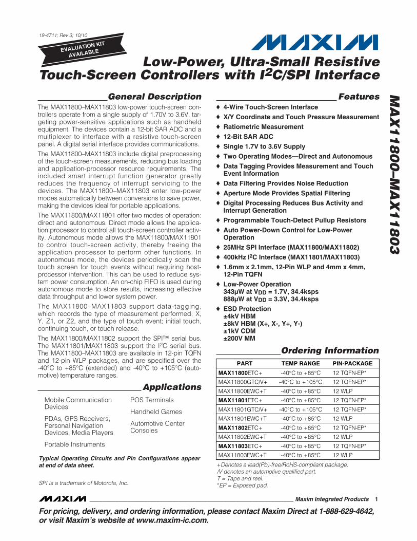
General DescriptionThe MAX11800–MAX11803 low-power touch-screen con-trollers operate from a single supply of 1.70V to 3.6V, tar-geting power-sensitive applications such as handheldequipment. The devices contain a 12-bit SAR ADC and amultiplexer to interface with a resistive touch-screenpanel. A digital serial interface provides communications.
The MAX11800–MAX11803 include digital preprocessingof the touch-screen measurements, reducing bus loadingand application-processor resource requirements. Theincluded smart interrupt function generator greatlyreduces the frequency of interrupt servicing to thedevices. The MAX11800–MAX11803 enter low-powermodes automatically between conversions to save power,making the devices ideal for portable applications.
The MAX11800/MAX11801 offer two modes of operation:direct and autonomous. Direct mode allows the applica-tion processor to control all touch-screen controller activ-ity. Autonomous mode allows the MAX11800/MAX11801to control touch-screen activity, thereby freeing theapplication processor to perform other functions. Inautonomous mode, the devices periodically scan thetouch screen for touch events without requiring host-processor intervention. This can be used to reduce sys-tem power consumption. An on-chip FIFO is used duringautonomous mode to store results, increasing effectivedata throughput and lower system power.
The MAX11800–MAX11803 support data-tagging,which records the type of measurement performed; X,Y, Z1, or Z2, and the type of touch event; initial touch,continuing touch, or touch release.
The MAX11800/MAX11802 support the SPI™ serial bus.The MAX11801/MAX11803 support the I2C serial bus.The MAX11800–MAX11803 are available in 12-pin TQFNand 12-pin WLP packages, and are specified over the -40°C to +85°C (extended) and -40°C to +105°C (auto-motive) temperature ranges.
Applications
Features♦ 4-Wire Touch-Screen Interface
♦ X/Y Coordinate and Touch Pressure Measurement
♦ Ratiometric Measurement
♦ 12-Bit SAR ADC
♦ Single 1.7V to 3.6V Supply
♦ Two Operating Modes—Direct and Autonomous
♦ Data Tagging Provides Measurement and TouchEvent Information
♦ Data Filtering Provides Noise Reduction
♦ Aperture Mode Provides Spatial Filtering
♦ Digital Processing Reduces Bus Activity andInterrupt Generation
♦ Programmable Touch-Detect Pullup Resistors
♦ Auto Power-Down Control for Low-PowerOperation
♦ 25MHz SPI Interface (MAX11800/MAX11802)
♦ 400kHz I2C Interface (MAX11801/MAX11803)
♦ 1.6mm x 2.1mm, 12-Pin WLP and 4mm x 4mm,12-Pin TQFN
♦ Low-Power Operation343µW at VDD = 1.7V, 34.4ksps888µW at VDD = 3.3V, 34.4ksps
♦ ESD Protection±4kV HBM±8kV HBM (X+, X-, Y+, Y-)±1kV CDM±200V MM
MA
X1
18
00
–MA
X1
18
03
Low-Power, Ultra-Small Resistive Touch-Screen Controllers with I2C/SPI Interface
________________________________________________________________ Maxim Integrated Products 1
Ordering Information
19-4711; Rev 3; 10/10
For pricing, delivery, and ordering information, please contact Maxim Direct at 1-888-629-4642,or visit Maxim’s website at www.maxim-ic.com.
EVALUATION KIT
AVAILABLE
PART TEMP RANGE PIN-PACKAGE
MAX11800ETC+ -40°C to +85°C 12 TQFN-EP*
MAX11800GTC/V+ -40°C to +105°C 12 TQFN-EP*
MAX11800EWC+T -40°C to +85°C 12 WLP
MAX11801ETC+ -40°C to +85°C 12 TQFN-EP*
MAX11801GTC/V+ -40°C to +105°C 12 TQFN-EP*
MAX11801EWC+T -40°C to +85°C 12 WLP
MAX11802ETC+ -40°C to +85°C 12 TQFN-EP*
MAX11802EWC+T -40°C to +85°C 12 WLP
MAX11803ETC+ -40°C to +85°C 12 TQFN-EP*
MAX11803EWC+T -40°C to +85°C 12 WLP Typical Operating Circuits and Pin Configurations appearat end of data sheet. +Denotes a lead(Pb)-free/RoHS-compliant package.
/V denotes an automotive qualified part.T = Tape and reel.*EP = Exposed pad.
Mobile CommunicationDevices
PDAs, GPS Receivers,Personal NavigationDevices, Media Players
Portable Instruments
POS Terminals
Handheld Games
Automotive CenterConsoles
SPI is a trademark of Motorola, Inc.
MA
X1
18
00
–MA
X1
18
03
Low-Power, Ultra-Small Resistive Touch-ScreenControllers with I2C/SPI Interface
2 _______________________________________________________________________________________
TABLE OF CONTENTSAbsolute Maximum Ratings . . . . . . . . . . . . . . . . . . . . . . . . . . . . . . . . . . . . . . . . . . . . . . . . . . . . . . . . . . . . . . . . . . . . . .8Electrical Characteristics . . . . . . . . . . . . . . . . . . . . . . . . . . . . . . . . . . . . . . . . . . . . . . . . . . . . . . . . . . . . . . . . . . . . . . . .8I2C Timing Characteristics . . . . . . . . . . . . . . . . . . . . . . . . . . . . . . . . . . . . . . . . . . . . . . . . . . . . . . . . . . . . . . . . . . . . . . .9SPI Timing Characteristics . . . . . . . . . . . . . . . . . . . . . . . . . . . . . . . . . . . . . . . . . . . . . . . . . . . . . . . . . . . . . . . . . . . . . .10Typical Operating Characteristics . . . . . . . . . . . . . . . . . . . . . . . . . . . . . . . . . . . . . . . . . . . . . . . . . . . . . . . . . . . . . . . .12Pin Description . . . . . . . . . . . . . . . . . . . . . . . . . . . . . . . . . . . . . . . . . . . . . . . . . . . . . . . . . . . . . . . . . . . . . . . . . . . . . . .14Functional Diagrams . . . . . . . . . . . . . . . . . . . . . . . . . . . . . . . . . . . . . . . . . . . . . . . . . . . . . . . . . . . . . . . . . . . . . . . . . .15Detailed Description . . . . . . . . . . . . . . . . . . . . . . . . . . . . . . . . . . . . . . . . . . . . . . . . . . . . . . . . . . . . . . . . . . . . . . . . . . .16
Position Measurements . . . . . . . . . . . . . . . . . . . . . . . . . . . . . . . . . . . . . . . . . . . . . . . . . . . . . . . . . . . . . . . . . . . . . .16Pressure Measurements . . . . . . . . . . . . . . . . . . . . . . . . . . . . . . . . . . . . . . . . . . . . . . . . . . . . . . . . . . . . . . . . . . . . .19Touch-Detect Modes and Options . . . . . . . . . . . . . . . . . . . . . . . . . . . . . . . . . . . . . . . . . . . . . . . . . . . . . . . . . . . . .20
PUR and PUF . . . . . . . . . . . . . . . . . . . . . . . . . . . . . . . . . . . . . . . . . . . . . . . . . . . . . . . . . . . . . . . . . . . . . . . . . .21Idle Modes . . . . . . . . . . . . . . . . . . . . . . . . . . . . . . . . . . . . . . . . . . . . . . . . . . . . . . . . . . . . . . . . . . . . . . . . . . . .21
Features Available in the MAX11800–MAX11803 Averaging Modes . . . . . . . . . . . . . . . . . . . . . . . . . . . . . . . . . . .21Combined Commands . . . . . . . . . . . . . . . . . . . . . . . . . . . . . . . . . . . . . . . . . . . . . . . . . . . . . . . . . . . . . . . . . . .23Data Tagging . . . . . . . . . . . . . . . . . . . . . . . . . . . . . . . . . . . . . . . . . . . . . . . . . . . . . . . . . . . . . . . . . . . . . . . . . .23Low-Power Modes . . . . . . . . . . . . . . . . . . . . . . . . . . . . . . . . . . . . . . . . . . . . . . . . . . . . . . . . . . . . . . . . . . . . . .23
Features Available in the MAX11800/MAX11801 Only . . . . . . . . . . . . . . . . . . . . . . . . . . . . . . . . . . . . . . . . . . . . . .24Autonomous Mode . . . . . . . . . . . . . . . . . . . . . . . . . . . . . . . . . . . . . . . . . . . . . . . . . . . . . . . . . . . . . . . . . . . . . . . . .24Aperture . . . . . . . . . . . . . . . . . . . . . . . . . . . . . . . . . . . . . . . . . . . . . . . . . . . . . . . . . . . . . . . . . . . . . . . . . . . . . . . . . .24
Panel Setup, Measurement, and Scan Commands . . . . . . . . . . . . . . . . . . . . . . . . . . . . . . . . . . . . . . . . . . . . .24Direct Conversion Mode Operations . . . . . . . . . . . . . . . . . . . . . . . . . . . . . . . . . . . . . . . . . . . . . . . . . . . . . . . . . . . .24
Interrupt Modes . . . . . . . . . . . . . . . . . . . . . . . . . . . . . . . . . . . . . . . . . . . . . . . . . . . . . . . . . . . . . . . . . . . . . . . .24Panel Setup Commands . . . . . . . . . . . . . . . . . . . . . . . . . . . . . . . . . . . . . . . . . . . . . . . . . . . . . . . . . . . . . . . . .27Panel Measurement Commands . . . . . . . . . . . . . . . . . . . . . . . . . . . . . . . . . . . . . . . . . . . . . . . . . . . . . . . . . . .27Combined Commands . . . . . . . . . . . . . . . . . . . . . . . . . . . . . . . . . . . . . . . . . . . . . . . . . . . . . . . . . . . . . . . . . . .28Auxiliary Measurement Command . . . . . . . . . . . . . . . . . . . . . . . . . . . . . . . . . . . . . . . . . . . . . . . . . . . . . . . . . .28
Autonomous Conversion Mode . . . . . . . . . . . . . . . . . . . . . . . . . . . . . . . . . . . . . . . . . . . . . . . . . . . . . . . . . . . . . . . .31Measurement Operations . . . . . . . . . . . . . . . . . . . . . . . . . . . . . . . . . . . . . . . . . . . . . . . . . . . . . . . . . . . . . . . .32Combined Commands . . . . . . . . . . . . . . . . . . . . . . . . . . . . . . . . . . . . . . . . . . . . . . . . . . . . . . . . . . . . . . . . . . .32Delayed Touch Detection During Mode Transitions . . . . . . . . . . . . . . . . . . . . . . . . . . . . . . . . . . . . . . . . . . . . .33FIFO Memory . . . . . . . . . . . . . . . . . . . . . . . . . . . . . . . . . . . . . . . . . . . . . . . . . . . . . . . . . . . . . . . . . . . . . . . . . .33Clearing FIFO . . . . . . . . . . . . . . . . . . . . . . . . . . . . . . . . . . . . . . . . . . . . . . . . . . . . . . . . . . . . . . . . . . . . . . . . . .33FIFO Data Block Readback Structure . . . . . . . . . . . . . . . . . . . . . . . . . . . . . . . . . . . . . . . . . . . . . . . . . . . . . . .33FIFO Data Word Structure . . . . . . . . . . . . . . . . . . . . . . . . . . . . . . . . . . . . . . . . . . . . . . . . . . . . . . . . . . . . . . . .34Block Readback Operations . . . . . . . . . . . . . . . . . . . . . . . . . . . . . . . . . . . . . . . . . . . . . . . . . . . . . . . . . . . . . . .34Clearing Interrupt . . . . . . . . . . . . . . . . . . . . . . . . . . . . . . . . . . . . . . . . . . . . . . . . . . . . . . . . . . . . . . . . . . . . . . .34Aperture Modes and Options . . . . . . . . . . . . . . . . . . . . . . . . . . . . . . . . . . . . . . . . . . . . . . . . . . . . . . . . . . . . . .34Aperture Range Requirements . . . . . . . . . . . . . . . . . . . . . . . . . . . . . . . . . . . . . . . . . . . . . . . . . . . . . . . . . . . . .34FIFO Aperture Criteria . . . . . . . . . . . . . . . . . . . . . . . . . . . . . . . . . . . . . . . . . . . . . . . . . . . . . . . . . . . . . . . . . . . .35
Applications Information . . . . . . . . . . . . . . . . . . . . . . . . . . . . . . . . . . . . . . . . . . . . . . . . . . . . . . . . . . . . . . . . . . . . . . .35Using Aperture Mode . . . . . . . . . . . . . . . . . . . . . . . . . . . . . . . . . . . . . . . . . . . . . . . . . . . . . . . . . . . . . . . . . . . . . . .35
MA
X1
18
00
–MA
X1
18
03
Low-Power, Ultra-Small Resistive Touch-ScreenControllers with I2C/SPI Interface
_______________________________________________________________________________________ 3
TABLE OF CONTENTS (continued)Examples of Using Aperture Mode . . . . . . . . . . . . . . . . . . . . . . . . . . . . . . . . . . . . . . . . . . . . . . . . . . . . . . . . . . . . .36SPI Communication Sequence (MAX11800/MAX11802) . . . . . . . . . . . . . . . . . . . . . . . . . . . . . . . . . . . . . . . . . . . .38
SPI Configuration Register Write (MAX11800/MAX11802) . . . . . . . . . . . . . . . . . . . . . . . . . . . . . . . . . . . . . . . .38SPI Configuration or Result Register Read (MAX11800/MAX11802) . . . . . . . . . . . . . . . . . . . . . . . . . . . . . . . .39SPI Conversion Command (MAX11800/MAX11802) . . . . . . . . . . . . . . . . . . . . . . . . . . . . . . . . . . . . . . . . . . . .40
I2C-Supported Sequence (MAX11801/MAX11803) . . . . . . . . . . . . . . . . . . . . . . . . . . . . . . . . . . . . . . . . . . . . . . . .40Bit Transfer . . . . . . . . . . . . . . . . . . . . . . . . . . . . . . . . . . . . . . . . . . . . . . . . . . . . . . . . . . . . . . . . . . . . . . . . . . . . . . .40START and STOP Conditions . . . . . . . . . . . . . . . . . . . . . . . . . . . . . . . . . . . . . . . . . . . . . . . . . . . . . . . . . . . . . . . . .40Early STOP Conditions . . . . . . . . . . . . . . . . . . . . . . . . . . . . . . . . . . . . . . . . . . . . . . . . . . . . . . . . . . . . . . . . . . . . . .41Slave Address . . . . . . . . . . . . . . . . . . . . . . . . . . . . . . . . . . . . . . . . . . . . . . . . . . . . . . . . . . . . . . . . . . . . . . . . . . . . .41I2C Register Address . . . . . . . . . . . . . . . . . . . . . . . . . . . . . . . . . . . . . . . . . . . . . . . . . . . . . . . . . . . . . . . . . . . . . . .41Acknowledge . . . . . . . . . . . . . . . . . . . . . . . . . . . . . . . . . . . . . . . . . . . . . . . . . . . . . . . . . . . . . . . . . . . . . . . . . . . . . .41Write Data Format . . . . . . . . . . . . . . . . . . . . . . . . . . . . . . . . . . . . . . . . . . . . . . . . . . . . . . . . . . . . . . . . . . . . . . . . . .42Read Data Format . . . . . . . . . . . . . . . . . . . . . . . . . . . . . . . . . . . . . . . . . . . . . . . . . . . . . . . . . . . . . . . . . . . . . . . . . .43
Streamlined I2C Read Operations . . . . . . . . . . . . . . . . . . . . . . . . . . . . . . . . . . . . . . . . . . . . . . . . . . . . . . . . . .44I2C Conversion and Measurement Commands (MAX11801/MAX11803) . . . . . . . . . . . . . . . . . . . . . . . . . . . . . . . .45Command and Register Map . . . . . . . . . . . . . . . . . . . . . . . . . . . . . . . . . . . . . . . . . . . . . . . . . . . . . . . . . . . . . . . . .45
User-Accessible Registers . . . . . . . . . . . . . . . . . . . . . . . . . . . . . . . . . . . . . . . . . . . . . . . . . . . . . . . . . . . . . . . .45Status and Configuration Registers . . . . . . . . . . . . . . . . . . . . . . . . . . . . . . . . . . . . . . . . . . . . . . . . . . . . . . . . .46
Data Readback Commands . . . . . . . . . . . . . . . . . . . . . . . . . . . . . . . . . . . . . . . . . . . . . . . . . . . . . . . . . . . . . . . . . .46Autonomous Conversion Mode . . . . . . . . . . . . . . . . . . . . . . . . . . . . . . . . . . . . . . . . . . . . . . . . . . . . . . . . . . . .46Direct Conversion Mode . . . . . . . . . . . . . . . . . . . . . . . . . . . . . . . . . . . . . . . . . . . . . . . . . . . . . . . . . . . . . . . . . .46
Panel Setup and Measurement Commands . . . . . . . . . . . . . . . . . . . . . . . . . . . . . . . . . . . . . . . . . . . . . . . . . . . . . .48User Configuration Registers . . . . . . . . . . . . . . . . . . . . . . . . . . . . . . . . . . . . . . . . . . . . . . . . . . . . . . . . . . . . . . . . . . . .49
General Status Register (0x00) (Read Only) . . . . . . . . . . . . . . . . . . . . . . . . . . . . . . . . . . . . . . . . . . . . . . . . . . . . . .49General Configuration Register (0x01) . . . . . . . . . . . . . . . . . . . . . . . . . . . . . . . . . . . . . . . . . . . . . . . . . . . . . . . . . .50Measurement Resolution Configuration Register (0x02) . . . . . . . . . . . . . . . . . . . . . . . . . . . . . . . . . . . . . . . . . . . . .50Measurement Averaging Configuration Register (0x03) . . . . . . . . . . . . . . . . . . . . . . . . . . . . . . . . . . . . . . . . . . . . .51ADC Sampling Time Configuration Register (0x04) . . . . . . . . . . . . . . . . . . . . . . . . . . . . . . . . . . . . . . . . . . . . . . . .51Panel Setup Timing Configuration Register (0x05) . . . . . . . . . . . . . . . . . . . . . . . . . . . . . . . . . . . . . . . . . . . . . . . . .52Delayed Conversion Configuration Register (0x06) . . . . . . . . . . . . . . . . . . . . . . . . . . . . . . . . . . . . . . . . . . . . . . . .52Touch-Detect Pullup Timing Configuration Register (0x07) . . . . . . . . . . . . . . . . . . . . . . . . . . . . . . . . . . . . . . . . . .53Autonomous Mode Timing Configuration Register (0x08) . . . . . . . . . . . . . . . . . . . . . . . . . . . . . . . . . . . . . . . . . . .54Aperture Configuration Register (0x09) . . . . . . . . . . . . . . . . . . . . . . . . . . . . . . . . . . . . . . . . . . . . . . . . . . . . . . . . .54Auxiliary Measurement Configuration Register (0x0A) . . . . . . . . . . . . . . . . . . . . . . . . . . . . . . . . . . . . . . . . . . . . . .55Operating Mode Configuration Register (0x0B) . . . . . . . . . . . . . . . . . . . . . . . . . . . . . . . . . . . . . . . . . . . . . . . . . . .56
MAX11800/MAX11802 Typical Operating Circuit . . . . . . . . . . . . . . . . . . . . . . . . . . . . . . . . . . . . . . . . . . . . . . . . . . . .57MAX11801/MAX11803 Typical Operating Circuit . . . . . . . . . . . . . . . . . . . . . . . . . . . . . . . . . . . . . . . . . . . . . . . . . . . .57Pin Configurations . . . . . . . . . . . . . . . . . . . . . . . . . . . . . . . . . . . . . . . . . . . . . . . . . . . . . . . . . . . . . . . . . . . . . . . . . . . .58Chip Information . . . . . . . . . . . . . . . . . . . . . . . . . . . . . . . . . . . . . . . . . . . . . . . . . . . . . . . . . . . . . . . . . . . . . . . . . . . . . .58Package Information . . . . . . . . . . . . . . . . . . . . . . . . . . . . . . . . . . . . . . . . . . . . . . . . . . . . . . . . . . . . . . . . . . . . . . . . . .58Revision History . . . . . . . . . . . . . . . . . . . . . . . . . . . . . . . . . . . . . . . . . . . . . . . . . . . . . . . . . . . . . . . . . . . . . . . . . . . . . .59
MA
X1
18
00
–MA
X1
18
03
Low-Power, Ultra-Small Resistive Touch-ScreenControllers with I2C/SPI Interface
4 _______________________________________________________________________________________
Figure 1. I2C Timing Diagram . . . . . . . . . . . . . . . . . . . . . . . . . . . . . . . . . . . . . . . . . . . . . . . . . . . . . . . . . . . . . . . . . . .10
Figure 2. SPI Timing Diagram . . . . . . . . . . . . . . . . . . . . . . . . . . . . . . . . . . . . . . . . . . . . . . . . . . . . . . . . . . . . . . . . . . .11
Figure 3a. MAX11800/MAX11801 Operation Modes . . . . . . . . . . . . . . . . . . . . . . . . . . . . . . . . . . . . . . . . . . . . . . . . . .17
Figure 3b. MAX11802/MAX11803 Operation Modes . . . . . . . . . . . . . . . . . . . . . . . . . . . . . . . . . . . . . . . . . . . . . . . . . .18
Figure 4. Position Measurements . . . . . . . . . . . . . . . . . . . . . . . . . . . . . . . . . . . . . . . . . . . . . . . . . . . . . . . . . . . . . . . . .19
Figure 5. Pressure Measurements . . . . . . . . . . . . . . . . . . . . . . . . . . . . . . . . . . . . . . . . . . . . . . . . . . . . . . . . . . . . . . . .19
Figure 6. Touch-Detection Circuitry . . . . . . . . . . . . . . . . . . . . . . . . . . . . . . . . . . . . . . . . . . . . . . . . . . . . . . . . . . . . . . .21
Figure 7. Touch-Detection Operations . . . . . . . . . . . . . . . . . . . . . . . . . . . . . . . . . . . . . . . . . . . . . . . . . . . . . . . . . . . . .22
Figure 8. State Machine Transitions (Direct Conversion Mode)—MAX11800–MAX11803 . . . . . . . . . . . . . . . . . . . . .25
Figure 9. Continuous Interrupt Mode (Direct Conversion Mode) . . . . . . . . . . . . . . . . . . . . . . . . . . . . . . . . . . . . . . . . .26
Figure 10. Edge Interrupt Mode (Direct Conversion Mode)—MAX11800–MAX11803 . . . . . . . . . . . . . . . . . . . . . . . .27
Figure 11. Command and Measurement Flow (DCM) . . . . . . . . . . . . . . . . . . . . . . . . . . . . . . . . . . . . . . . . . . . . . . . . .28
Figure 12. Panel Setup and Measurement Commands—MAX11800–MAX11803 . . . . . . . . . . . . . . . . . . . . . . . . . . .29
Figure 13. Combined Commands—MAX11800–MAX11803 . . . . . . . . . . . . . . . . . . . . . . . . . . . . . . . . . . . . . . . . . . . .30
Figure 14. State Machine Transitions––Autonomous Conversion Mode—MAX11800/MAX11801 . . . . . . . . . . . . . . .31
Figure 15. Clear-on-Read Interrupt Operation—MAX11800/MAX11801 . . . . . . . . . . . . . . . . . . . . . . . . . . . . . . . . . . .32
Figure 16. Aperture Usage Example Waveforms—MAX11800/MAX11801 . . . . . . . . . . . . . . . . . . . . . . . . . . . . . . . . .36
Figure 17. SPI Single Configuration Register Write Sequence—MAX11800/MAX11802 . . . . . . . . . . . . . . . . . . . . . .38
Figure 18. SPI Multiple Configuration Register Write Sequence—MAX11800/MAX11802 . . . . . . . . . . . . . . . . . . . . .38
Figure 19. SPI Single-Byte Register Read Sequence—MAX11800/MAX11802 . . . . . . . . . . . . . . . . . . . . . . . . . . . . .39
Figure 20. SPI Multiple-Byte Register Read Sequence—MAX11800/MAX11802 . . . . . . . . . . . . . . . . . . . . . . . . . . . .40
Figure 21. SPI Conversion Command—MAX11800/MAX11802 . . . . . . . . . . . . . . . . . . . . . . . . . . . . . . . . . . . . . . . . .40
Figure 22. 2-Wire Interface Timing Diagram . . . . . . . . . . . . . . . . . . . . . . . . . . . . . . . . . . . . . . . . . . . . . . . . . . . . . . . .41
Figure 23. START, STOP, and Repeated START Conditions . . . . . . . . . . . . . . . . . . . . . . . . . . . . . . . . . . . . . . . . . . . .41
Figure 24. Acknowledge . . . . . . . . . . . . . . . . . . . . . . . . . . . . . . . . . . . . . . . . . . . . . . . . . . . . . . . . . . . . . . . . . . . . . . .41
Figure 25. I2C Single Write Sequence . . . . . . . . . . . . . . . . . . . . . . . . . . . . . . . . . . . . . . . . . . . . . . . . . . . . . . . . . . . . .42
Figure 26. I2C Multiple Write Sequence . . . . . . . . . . . . . . . . . . . . . . . . . . . . . . . . . . . . . . . . . . . . . . . . . . . . . . . . . . . .42
Figure 27. Basic Single Read Sequence . . . . . . . . . . . . . . . . . . . . . . . . . . . . . . . . . . . . . . . . . . . . . . . . . . . . . . . . . . .43
Figure 28. I2C Multiple Read Sequence . . . . . . . . . . . . . . . . . . . . . . . . . . . . . . . . . . . . . . . . . . . . . . . . . . . . . . . . . . .43
Figure 29. I2C Streamlined Read Sequence . . . . . . . . . . . . . . . . . . . . . . . . . . . . . . . . . . . . . . . . . . . . . . . . . . . . . . . .44
Figure 30. I2C Conversion and Measurement Commands . . . . . . . . . . . . . . . . . . . . . . . . . . . . . . . . . . . . . . . . . . . . .45
LIST OF FIGURES
MA
X1
18
00
–MA
X1
18
03
Low-Power, Ultra-Small Resistive Touch-ScreenControllers with I2C/SPI Interface
_______________________________________________________________________________________ 5
LIST OF TABLESTable 1. Terminology . . . . . . . . . . . . . . . . . . . . . . . . . . . . . . . . . . . . . . . . . . . . . . . . . . . . . . . . . . . . . . . . . . . . . . . . . . .6
Table 2. Operating Modes, Conditions, and Options . . . . . . . . . . . . . . . . . . . . . . . . . . . . . . . . . . . . . . . . . . . . . . . . .19
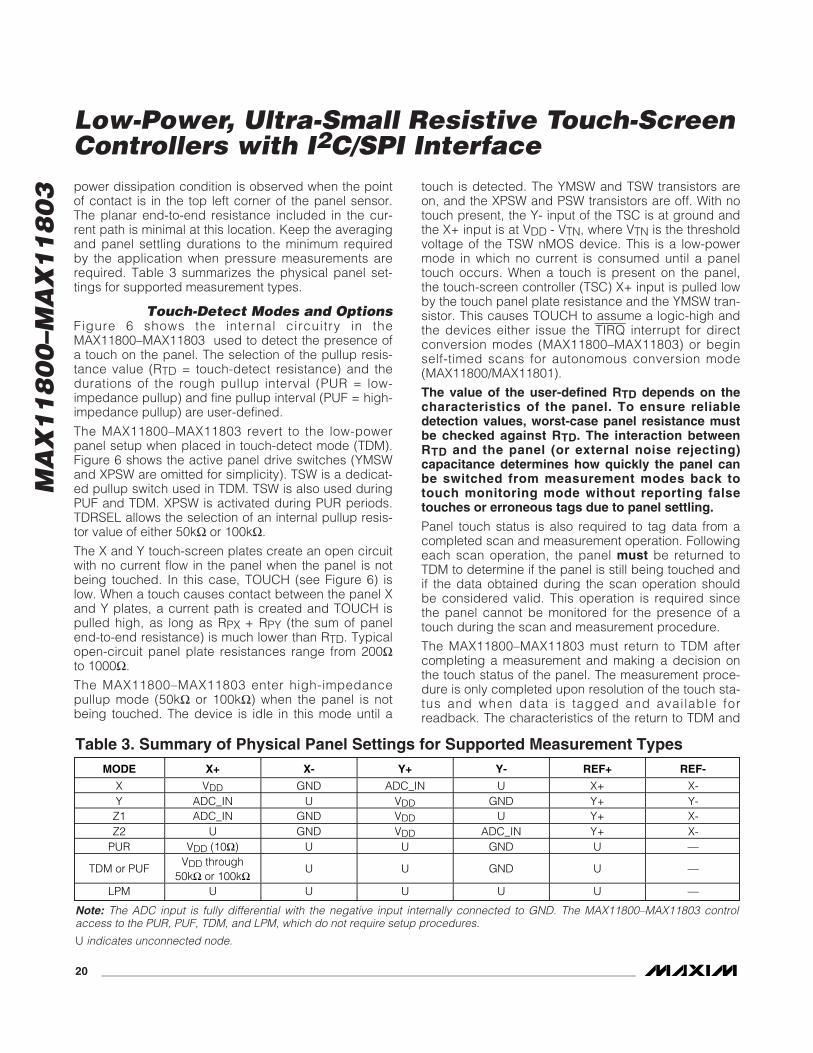
Table 3. Summary of Physical Panel Settings for Supported Measurement Types . . . . . . . . . . . . . . . . . . . . . . . . . . .20
Table 4. Median Averaging Operations . . . . . . . . . . . . . . . . . . . . . . . . . . . . . . . . . . . . . . . . . . . . . . . . . . . . . . . . . . . .23
Table 5. Data Word Structure (All Direct Conversion Modes) . . . . . . . . . . . . . . . . . . . . . . . . . . . . . . . . . . . . . . . . . . .23
Table 6. Measurement and Event Tags (Continuous Interrupt Mode) . . . . . . . . . . . . . . . . . . . . . . . . . . . . . . . . . . . . .25
Table 7. Measurement and Event Tags (Edge Interrupt Mode) . . . . . . . . . . . . . . . . . . . . . . . . . . . . . . . . . . . . . . . . .26
Table 8. Panel Setup Command Summary . . . . . . . . . . . . . . . . . . . . . . . . . . . . . . . . . . . . . . . . . . . . . . . . . . . . . . . . .27
Table 9. Panel Measurement Command Summary . . . . . . . . . . . . . . . . . . . . . . . . . . . . . . . . . . . . . . . . . . . . . . . . . . .28
Table 10. FIFO Data Block Structure . . . . . . . . . . . . . . . . . . . . . . . . . . . . . . . . . . . . . . . . . . . . . . . . . . . . . . . . . . . . . .33
Table 11. FIFO Data Word Structure . . . . . . . . . . . . . . . . . . . . . . . . . . . . . . . . . . . . . . . . . . . . . . . . . . . . . . . . . . . . . .34
Table 12. FIFO Data Measurement Tags . . . . . . . . . . . . . . . . . . . . . . . . . . . . . . . . . . . . . . . . . . . . . . . . . . . . . . . . . . .34
Table 13. FIFO Event Tags . . . . . . . . . . . . . . . . . . . . . . . . . . . . . . . . . . . . . . . . . . . . . . . . . . . . . . . . . . . . . . . . . . . . . .34
Table 14. Readback and FIFO Contents with Aperture Mode Enabled . . . . . . . . . . . . . . . . . . . . . . . . . . . . . . . . . . .37
Table 15. Readback and FIFO Contents with Aperture Mode Disabled . . . . . . . . . . . . . . . . . . . . . . . . . . . . . . . . . . .37
Table 16. SPI Command and Data Format: 8 Bits . . . . . . . . . . . . . . . . . . . . . . . . . . . . . . . . . . . . . . . . . . . . . . . . . . . .46
Table 17. I2C Command and Data Format: 8 Bits Plus ACK . . . . . . . . . . . . . . . . . . . . . . . . . . . . . . . . . . . . . . . . . . . .46
Table 18. Status and Configuration Registers . . . . . . . . . . . . . . . . . . . . . . . . . . . . . . . . . . . . . . . . . . . . . . . . . . . . . .47
Table 19. Data Readback Command Summary . . . . . . . . . . . . . . . . . . . . . . . . . . . . . . . . . . . . . . . . . . . . . . . . . . . . .47
Table 20. Conversion Command Summary . . . . . . . . . . . . . . . . . . . . . . . . . . . . . . . . . . . . . . . . . . . . . . . . . . . . . . . . .48
Table 21. Measurement Commands . . . . . . . . . . . . . . . . . . . . . . . . . . . . . . . . . . . . . . . . . . . . . . . . . . . . . . . . . . . . . .49
MA
X1
18
00
–MA
X1
18
03
Low-Power, Ultra-Small Resistive Touch-ScreenControllers with I2C/SPI Interface
6 _______________________________________________________________________________________
TERM DEFINITION
Panel, Touch Screen, Touch Panel
Resistive Touch Sensor: Panel, or touch screen, or touch panel are used interchangeably to denote the resistive touch sensor.
TSCTouch-Screen Controller: Devices attached to a touch screen that provide the interface between an application processor (AP) and touch screen.
X+X Position Positive I/O: Analog I/O from resistive touch screen. See Figure 4 for configuration and measurement details.
X-X Position Negative I/O: Analog I/O from resistive touch screen. See Figure 4 for configuration and measurement details.
Y+Y Position Positive I/O: Analog I/O from resistive touch screen. See Figure 4 for configuration and measurement details.
Y-Y Position Negative I/O: Analog I/O from resistive touch screen. See Figure 4 for configuration and measurement details.
RTOUCHTouch Resistance: Represents the resistance between the X and Y planes of a resistive touch screen during a touch event.
Z1Z1 Measurement: A resistive touch-screen measurement to determine the resistance between the two planes within the panel sensor during a touch event (RTOUCH). See Figure 5 for configuration and measurement details.
Z2Z2 Measurement: A resistive touch-screen measurement to determine the resistance between the two planes within the panel sensor during a touch event (RTOUCH). See Figure 5 for configuration and measurement details.
AUXAuxiliary Input: Analog input to the MAX11800–MAX11803 that can be used to monitor external conditions such as battery voltage or temperature.
ADC Analog-to-Digital Converter: Circuit used to transform analog information into a form suitable for digital operations.
APApplication Processor: An external microcontroller or microprocessor that interfaces to and controls the general operation of the MAX11800–MAX11803.
AVGAveraging Mode: The ability to average consecutive measurement results to reduce noise from switch bounce, power-supply ripple, and incomplete settling.
MAFMedian Averaging Filter: The MAF first removes the minimum and maximum samples before taking the average of the remaining sample set.
SAF Straight Averaging Filter: The SAF takes the average of an entire sample set.
TDMTouch-Detect Mode: An untimed mode that monitors the panel for a touch using a user-selectable panel pullup resistor of either 50k or 100k .
DCMDirect Conversion Mode: A mode of operation in which the AP requests individual panel setup and conversion operations or automated combinations of measurements (X and Y, X and Y and Z1, or X and Y and Z1 and Z2). The AP maintains control over the initiation of panel setup, measurements, and the sampling f
ACMAutonomous Conversion Mode: A mode of operation in which the MAX11800/MAX11801 idle in TDM until a touch event occurs. After a touch is detected, the MAX11800/MAX11801 begin an automated sequence of measurements determined by the user configuration registers.
PSU
Panel Setup Command: User-programmable modes for the purpose of allowing the panel sufficient time to settle, prior to the start of measurements. PSU commands configure the on-chip multiplexer in preparation to perform either X, Y, Z1, or Z2 measurements. Durations can either be specified and managed by the MAX11800–MAX11803 (in ACM and DCM) or managed by the AP (in DCM).
PMC Panel Measurement Command: Individual measurements of X or Y position and Z1 or Z2 pressure measurements.
CMCCombined Measurement Command: Combinations of PMCs (X and Y, X and Y and Z1, or X and Y and Z1 and Z2) offered by the MAX11800–MAX11803 and executed in series to reduce AP bus and interrupt activity.
Table 1. Terminology
MA
X1
18
00
–MA
X1
18
03
Low-Power, Ultra-Small Resistive Touch-ScreenControllers with I2C/SPI Interface
_______________________________________________________________________________________ 7
TERM DEFINITION
FIFOFirst-In First-Out Memory: The MAX11800–MAX11803 contain a 1024-bit FIFO that is used to store conversionresults when operating in autonomous conversion mode. FIFO depth indicates the number of words (16-bitquantity) in the FIFO.
ScanScan: Generally, a single sequence of operations performed in DCM or ACM. The operations could include apanel setup operation, followed by a panel measurement operation, or a combined measurement operation.
Scan BlockScan Block: Generally, a sequence of multiple operations performed in DCM or ACM. The operations couldinclude panel-setup operations, panel-measurement operations, or combined measurement operations.
Timed ScanTimed Scan: A scan or scan block operation that uses the on-chip oscillator and timer. The timer is controlledthrough the configuration registers and represents an array of fixed (time) quantities that are user selectable(MAX11800/MAX11801).
Untimed Scan Untimed Scan: A scan or scan block operation that is controlled by the AP. This only applies to DCM.
TAGD a t a Ta g : Infor m ati on ap p end ed to the end of an AD C conver si on r esul t. Tag s i nd i cate the typ e of m easur em ent and touch status associ ated w i th each p anel ob ser vati on. S ee the d efi ni ti ons for E TAG and M TAG ( al so i n Tab l e 1) .
ETAG Event Tag: Data tags indicating the panel touch status observed during a measurement.
MTAG Measurement Tag: Data tag indicating the type of measurement read back by the AP (either X, Y, Z1, or Z2).
TIRQTouch Interrupt Request: Active-low interrupt, indicating that a touch is present (CINT) or has been initiated(EINT) in DCM, or that new data is available in the FIFO in ACM.
EINTEdge Interrupt Mode: Indicates, through TIRQ, that a touch has been initiated (EINT) in DCM. The duration thatTIRQ is low is user programmable.
CINTContinuous Interrupt Mode: Indicates, through TIRQ, that a touch is present (CINT) in DCM. TIRQ goes low toindicate the presence of a touch and stays low until the touch event ceases.
CORINTClear-on-Read Interrupt Mode: Used in ACM only. TIRQ goes low to indicate the presence of new FIFO data. Theinterrupt is cleared when the data is read by the AP (MAX11800/MAX11801).
APER Aperture Mode: Available in ACM only. Reduces data writes to the FIFO by spatially filtering measurement data.
CONTC o n t i n u o u s B i t : An op ti on i n D C M to r etur n the MAX11800–MAX11803 to a p anel setup ( w ai t) m od e ( P S U ) after aconver si on, r ather than a r etur n to TD M ( r ecom m end ed onl y for ap p l i cati ons w i th ver y l ong p anel settl i ng ti m es and r eq uest contr ol l i ng thei r ow n aver ag i ng ) . The conti nuous b i t r esi d es i n b i t 0 ( R0) of the P S U and P M C r eg i ster s.
LPMLow-Power Mode: An idle mode used in DCM/EINT or ACM modes, when a touch is detected at the conclusion ofthe last measurement. This indicates a new measurement needs to be requested or scheduled (the touch-detectpullup is not engaged to save power).
PURPullup Rough: A fast pullup mode, which uses the main X+ switch in parallel with the on-chip resistive pullup(50kΩ/100kΩ) to quickly slew the touch panel capacitances. RPUR ≤ 10Ω typical.
PUFPullup Fine: A slow (fine) pullup mode, which uses the on-chip resistive pullup to slew the touch-panelcapacitances to their final values (RPUF = 50kΩ or 100kΩ) typical and is required for all applications.
SAR ADCSuccessive Approximation Register ADC: An analog-to-digital converter that converts a continuous analogwaveform into a discrete digital representation through a binary search through all possible quantization levelsbefore finally converging upon a digital output for each conversion.
I2CInter-Integrated Circuit: A multimaster serial computer bus that is used to attach low-speed peripherals to othercomponents using two bidirectional open-drain lines, serial data (SDA) and serial clock (SCL), pulled up withresistors.
SPISerial Peripheral Interface: A serial interface in which a master device supplies clock pulses to exchange dataserially with a slave over two data wires (master-slave and slave-master).
Table 1. Terminology (continued)
MA
X1
18
00
–MA
X1
18
03
Low-Power, Ultra-Small Resistive Touch-ScreenControllers with I2C/SPI Interface
8 _______________________________________________________________________________________
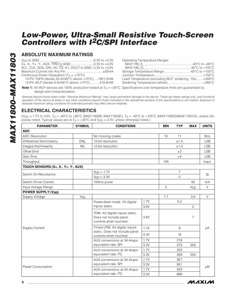
ELECTRICAL CHARACTERISTICS(VDD = 1.7V to 3.6V, TA = -40°C to +85°C (MAX11800E–MAX11803E), TA = -40°C to +105°C (MAX11800G/MAX11801G), unless oth-erwise noted. Typical values are at TA = +25°C and VDD = 3.3V, unless otherwise noted.)
Stresses beyond those listed under “Absolute Maximum Ratings” may cause permanent damage to the device. These are stress ratings only, and functionaloperation of the device at these or any other conditions beyond those indicated in the operational sections of the specifications is not implied. Exposure toabsolute maximum rating conditions for extended periods may affect device reliability.
VDD to GND...........................................................-0.3V to +4.0VX+, X-, Y+, Y-, AUX, TIRQ to GND ........................-0.3V to +4.0VSCL, CLK, SDA, DIN, A0, CS, A1, DOUT to GND.-0.3V to +4.0VMaximum Current into Any Pin .........................................±50mAContinuous Power Dissipation (TA = +70°C)
12-Pin TQFN (derate 24.4mW/°C above +70°C) ....1951.2mW12-Pin WLP (derate 6.5mW/°C above +70°C) ..........518.8mW
Operating Temperature RangesMAX1180_E_ _..................................................-40°C to +85°CMAX1180_G_ _ ...............................................-40°C to +105°C
Storage Temperature Range .............................-65°C to +150°CJunction Temperature ......................................................+150°CLead Temperature (excluding WLP, soldering, 10s) .......+300°CSoldering Temperature (reflow) .......................................+260°C
PARAMETER SYMBOL CONDITIONS MIN TYP MAX UNITS
ADC
ADC Resolution No missing codes 10 11 Bits
Differential Nonlinearity DNL 12-bit resolution ±1.5 LSB
Integral Nonlinearity INL 12-bit resolution ±1.5 LSB
Offset Error ±2 LSB
Gain Error ±4 LSB
Throughput 105 ksps
TOUCH SENSORS (X+, X-, Y+, Y-, AUX)
VDD = 1.7V 7 Switch On-Resistance
VDD = 3.3V 5
Switch Driver Current 100ms pulse 50 mA
Input Voltage Range 0 VDD V
POWER SUPPLY (VDD)Supply Voltage VDD 1.7 3.6 V
1.7V 0.2 Power-down mode. All digital inputs static. 3.6V 2
TDM. All digital inputs static. Does not include panel currents when touched.
3.6V 7
1.7V 9 Timed LPM. All digital inputs static. Does not include panel currents when touched. 3.3V 16
1.7V 216 AUX conversions at 34.4ksps equivalent rate, SPI 3.3V 273 550
1.7V 202
Supply Current
AUX conversions at 34.4ksps equivalent rate, I2C 3.3V 269 550
μA
1.7V 367 AUX conversions at 34.4ksps equivalent rate, SPI 3.3V 901
1.7V 343 Power Consumption
AUX conversions at 34.4ksps equivalent rate, I2C 3.3V 888
μW
ABSOLUTE MAXIMUM RATINGS
Note 1: All WLP devices are 100% production tested at TA = +25°C. Specifications over temperature limits are guaranteed bydesign and characterization.
MA
X1
18
00
–MA
X1
18
03
Low-Power, Ultra-Small Resistive Touch-ScreenControllers with I2C/SPI Interface
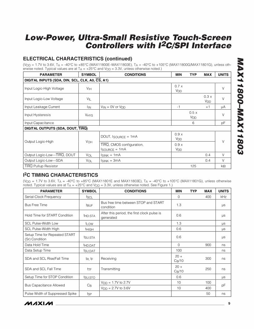
_______________________________________________________________________________________ 9
PARAMETER SYMBOL CONDITIONS MIN TYP MAX UNITS
DIGITAL INPUTS (SDA, DIN, SCL, CLK, A0, CS, A1)
Input Logic-High Voltage VIH0.7 x VDD
V
Input Logic-Low Voltage VIL 0.3 x VDD
V
Input Leakage Current IIN VIN = 0V or VDD -1 +1 μA
Input Hysteresis VHYS 0.5 x VDD
V
Input Capacitance 6 pF
DIGITAL OUTPUTS (SDA, DOUT, TIRQ)
DOUT, ISOURCE = 1mA 0.9 x VDD
Output Logic-High VOHTIRQ, CMOS configuration, ISOURCE = 1mA
0.9 x VDD
V
Output Logic-Low—TIRQ, DOUT VOL ISINK = 1mA 0.4 V
Output Logic-Low—SDA VOL ISINK = 3mA 0.4 V
TIRQ Pullup Resistor 125 k
ELECTRICAL CHARACTERISTICS (continued)(VDD = 1.7V to 3.6V, TA = -40°C to +85°C (MAX11800E–MAX11803E), TA = -40°C to +105°C (MAX11800G/MAX11801G), unless oth-erwise noted. Typical values are at TA = +25°C and VDD = 3.3V, unless otherwise noted.)
I2C TIMING CHARACTERISTICS(VDD = 1.7V to 3.6V, TA = -40°C to +85°C (MAX11801E and MAX11803E), TA = -40°C to +105°C (MAX11801G), unless otherwisenoted. Typical values are at TA = +25°C and VDD = 3.3V, unless otherwise noted. See Figure 1.)
PARAMETER SYMBOL CONDITIONS MIN TYP MAX UNITS
Serial-Clock Frequency fSCL 0 400 kHz
Bus Free Time tBUFBus free time between STOP and STARTcondition
1.3 μs
Hold Time for START Condition tHD;STAAfter this period, the first clock pulse isgenerated
0.6 μs
SCL Pulse-Width Low tLOW 1.3 μs
SCL Pulse-Width High tHIGH 0.6 μs
Setup Time for Repeated START(Sr) Condition
tSU;STA 0.6 μs
Data Hold Time tHD;DAT 0 900 ns
Data Setup Time tSU;DAT 100 ns
SDA and SCL Rise/Fall Time tR, tF Receiving20 +
CB/10300 ns
SDA and SCL Fall Time tTF Transmitting20 +
CB/10250 ns
Setup Time for STOP Condition tSU;STO 0.6 μs
VDD = 1.7V to 2.7V 10 100Bus Capacitance Allowed CB
VDD = 2.7V to 3.6V 10 400pF
Pulse Width of Suppressed Spike tSP 50 ns
MA
X1
18
00
–MA
X1
18
03
Low-Power, Ultra-Small Resistive Touch-ScreenControllers with I2C/SPI Interface
10 ______________________________________________________________________________________
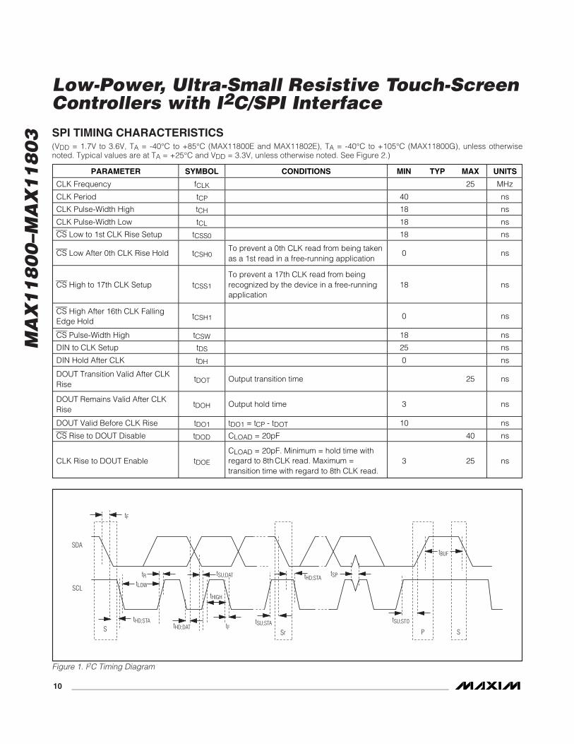
SPI TIMING CHARACTERISTICS(VDD = 1.7V to 3.6V, TA = -40°C to +85°C (MAX11800E and MAX11802E), TA = -40°C to +105°C (MAX11800G), unless otherwisenoted. Typical values are at TA = +25°C and VDD = 3.3V, unless otherwise noted. See Figure 2.)
PARAMETER SYMBOL CONDITIONS MIN TYP MAX UNITS
CLK Frequency fCLK 25 MHz
CLK Period tCP 40 ns
CLK Pulse-Width High tCH 18 ns
CLK Pulse-Width Low tCL 18 ns
CS Low to 1st CLK Rise Setup tCSS0 18 ns
CS Low After 0th CLK Rise Hold tCSH0To prevent a 0th CLK read from being takenas a 1st read in a free-running application
0 ns
CS High to 17th CLK Setup tCSS1
To prevent a 17th CLK read from beingrecognized by the device in a free-runningapplication
18 ns
CS High After 16th CLK FallingEdge Hold
tCSH1 0 ns
CS Pulse-Width High tCSW 18 ns
DIN to CLK Setup tDS 25 ns
DIN Hold After CLK tDH 0 ns
DOUT Transition Valid After CLKRise
tDOT Output transition time 25 ns
DOUT Remains Valid After CLKRise
tDOH Output hold time 3 ns
DOUT Valid Before CLK Rise tDO1 tDO1 = tCP - tDOT 10 ns
CS Rise to DOUT Disable tDOD CLOAD = 20pF 40 ns
CLK Rise to DOUT Enable tDOE
CLOAD = 20pF. Minimum = hold time withregard to 8th CLK read. Maximum =transition time with regard to 8th CLK read.
3 25 ns
SDA
SCL
S
tF
tHD;STA
tLOW
tR
tHD;DAT
tSU;DAT
tHIGH
tFtSU;STA
tHD;STA
Sr
tSP
tBUF
tSU;STO
P S
Figure 1. I2C Timing Diagram
MA
X1
18
00
–MA
X1
18
03
Low-Power, Ultra-Small Resistive Touch-ScreenControllers with I2C/SPI Interface
______________________________________________________________________________________ 11
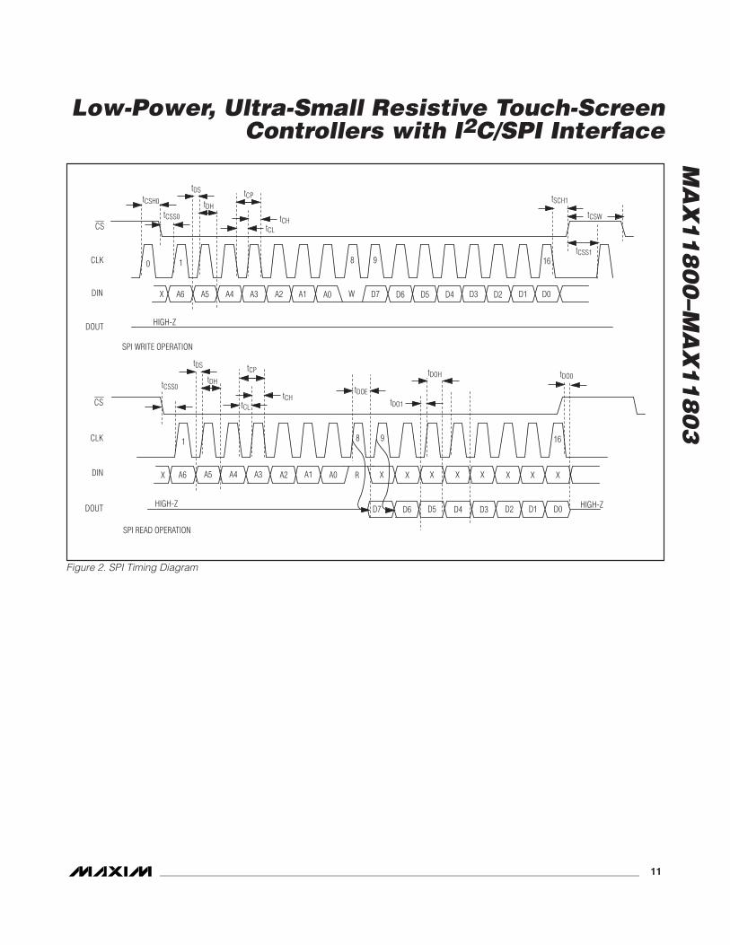
10 8 9 16
X A6 A5 A4 A3 A2 A1 A0 W D7 D6 D5 D4 D3 D2 D1 D0DIN
CLK
CS
tCSH0
tDS
tDH
tCLtCH
tCP
tCSW
tCSS1
tSCH1
DOUT HIGH-Z
SPI WRITE OPERATION
1 8 9 16
X A6 A5 A4 A3 A2 A1 A0 R X X X X X X X XDIN
CLK
CS
tCSS0
tDS
tDH
tCLtCH
tCP tDO0
DOUT HIGH-Z
SPI READ OPERATION
tDOEtDO1
tDOH
D7 D6 D5 D4 D3 D2 D1 D0 HIGH-Z
tCSS0
Figure 2. SPI Timing Diagram
MA
X1
18
00
–MA
X1
18
03
Low-Power, Ultra-Small Resistive Touch-ScreenControllers with I2C/SPI Interface
12 ______________________________________________________________________________________
AVERAGE SUPPLY CURRENTvs. SAMPLING RATE
MAX
1180
0 to
c01
SAMPLING RATE (cps)
SUPP
LY C
URRE
NT (F
A)
180160120 14040 60 80 10020
10
20
30
40
50
60
70
80
90
00 200
AUTONOMOUS MODEMAX11800MAX11801
cps = COORDINATES PER SECOND
DATA TAKEN WITHRESISTIVE TOUCHSENSOR
AVERAGE SUPPLY CURRENTvs. SAMPLING RATE
MAX
1180
0 to
c02
SAMPLING RATE (cps)
SUPP
LY C
URRE
NT (F
A)
18016014012010080604020
1
2
3
4
5
00 200
DIRECT CONTINUOUSINTERRUPT MODE
cps = COORDINATES PER SECOND
AVERAGE SUPPLY CURRENTvs. SAMPLING RATE
MAX
1180
0 to
c03
SAMPLING RATE (cps)
SUPP
LY C
URRE
NT (F
A)
18016014012010080604020
1
2
3
4
5
00 200
DIRECT EDGEINTERRUPT MODE
cps = COORDINATES PER SECOND
SUPPLY CURRENT IN POWER-DOWNvs. TEMPERATURE
MAX
1180
0 to
c04
TEMPERATURE (NC)
POW
ER-D
OWN
SUPP
LY C
URRE
NT (
µA)
603510-15
0.04
0.08
0.12
0.16
0.20
0.24
0.28
0.32
0.36
0.40
0-40 85
SWITCH RESISTANCEvs. SUPPLY VOLTAGE
MAX
1180
0 to
c05
VDD (V)
R ON
(I)
3.22.82.42.0
4
5
6Y+
7
8
31.6 3.6
X+ Y-
X-
SWITCH RESISTANCEvs. TEMPERATURE
MAX
1180
0 to
c06
TEMPERATURE (NC)
R ON
(I)
603510-15
2
3
4
5
6
7
1-40 85
X-
X+
Y-
Y+
CHANGE IN ADC GAINvs. TEMPERATURE
MAX
1180
0 to
c07
TEMPERATURE (NC)
DELT
A FR
OM +
25NC
(LSB
)
8050-10 20
-3
-2
-1
0
2
1
3
4
-4-40 110
CHANGE IN ADC OFFSETvs. TEMPERATURE
MAX
1180
0 to
c08
TEMPERATURE (NC)
DELT
A FR
OM +
25NC
(LSB
)
8050-10 20
-3
-2
-1
0
2
1
3
4
-4-40 110
Typical Operating Characteristics(VDD = 1.8V at TA = -40°C to +85°C (TA = -40°C, TA = 0°C, TA = +25°C, and TA = +85°C), 12-bit mode, all measurements usingnoncontinuous AUX input. SPI = 10MHz and I2C = 400kHz, unless otherwise noted. Resistive touch-screen panel (X+ to X- = 608Ω,Y+ to Y- = 371Ω).)
MA
X1
18
00
–MA
X1
18
03
Low-Power, Ultra-Small Resistive Touch-ScreenControllers with I2C/SPI Interface
______________________________________________________________________________________ 13
AVERAGE SUPPLY CURRENTvs. SAMPLING RATE
MAX
1180
0 to
c09
SAMPLING RATE (sps)
SUPP
LY C
URRE
NT (F
A)
18016014012010080604020
0.5
1.0
1.5
2.0
2.5
3.0
00 200
DIRECT CONVERSIONMODE—AUXILIARY INPUT
sps = SAMPLES PER SECOND
AVERAGE SUPPLY CURRENTvs. SAMPLING RATE
MAX
1180
0 to
c10
EQUIVALENT SAMPLING RATE (ksps)
SUPP
LY C
URRE
NT (F
A)
2416
20
40
60
80
100
120
08 32
AUXILIARY INPUT DATASAMPLED AT 1ksps AND2ksps WITH EIGHT AND16 SAMPLESAVERAGINGENABLED
ksps = KILO-SAMPLES PER SECOND
INTERNAL OSCILLATOR CLOCKFREQUENCY vs. TEMPERATURE
MAX
1180
0 to
c11
TEMPERATURE (NC)
INTE
RNAL
OSC
ILLA
TOR
CLOC
K FR
EQUE
NCY
(MHz
)
603510-15
1.92
1.94
1.96
1.98
2.00
2.02
2.04
2.06
2.08
1.90-40 85
VDD = 3.6V
VDD = 1.8V
VDD = 3.0V
INTERNAL OSCILLATOR CLOCKFREQUENCY vs. SUPPLY VOLTAGE
MAX
1180
0 to
c12
VDD (V)
INTE
RNAL
OSC
ILLA
TOR
CLOC
K FR
EQUE
NCY
(MHz
)
3.02.4
1.92
1.94
1.96
1.98
2.00
2.02
2.04
2.06
2.08
1.901.8 3.6
POWER CONSUMPTIONvs. SAMPLE RATE
MAX
1180
0 to
c13
SAMPLE RATE (cps)
POW
ER C
ONSU
MPT
ION
(FW
)
15010050
20
40
60
80
100
120
140
160
00 200
DATA TAKEN WITHRESISTIVE TOUCH SENSOR
AUTONOMOUS MODE*
*MAX11800/MAX11801
DIRECT CONTINUOUS MODE
DIRECT EDGE MODE
cps = COORDINATES PER SECOND
Typical Operating Characteristics (continued)(VDD = 1.8V at TA = -40°C to +85°C (TA = -40°C, TA = 0°C, TA = +25°C, and TA = +85°C), 12-bit mode, all measurements usingnoncontinuous AUX input. SPI = 10MHz and I2C = 400kHz, unless otherwise noted. Resistive touch-screen panel (X+ to X- = 608Ω,Y+ to Y- = 371Ω).)
MA
X1
18
00
–MA
X1
18
03
Low-Power, Ultra-Small Resistive Touch-ScreenControllers with I2C/SPI Interface
14 ______________________________________________________________________________________
Pin DescriptionPIN
MAX11800/MAX11802 MAX11801/MAX11803
TQFN-EP WLP TQFN-EP WLP
NAME FUNCTION
1 A4 1 A4 X+ X+ Channel Input/Output
2 B4 2 B4 VDD Power Supply. Bypass VDD to GND with a 1μF capacitor.
3 B3 3 B3 GND Ground
4 C4 4 C4 X- X- Channel Input/Output
5 C3 5 C3 Y- Y- Channel Input/Output
6 C2 6 C2 TIRQ Active-Low Touch Interrupt Output
7 C1 — —- DIN SPI Serial Data Input
8 B1 — — CLK SPI Serial Data Clock Input
9 A1 — — CS SPI Chip-Select Input
10 B2 — — DOUT SPI Data Output
11 A2 11 A2 AUX Auxiliary Input
12 A3 12 A3 Y+ Y+ Channel Input/Output
— — 7 C1 SDA I2C Serial Data Bus Input/Output
— — 8 B1 SCL I2C Serial Data Clock Input
— — 9 A1 A0 I2C Address Input Bit 0
— — 10 B2 A1 I2C Address Input Bit 1
— — — — EP Exposed Pad (TQFN only). Connected to ground.
MA
X1
18
00
–MA
X1
18
03
Low-Power, Ultra-Small Resistive Touch-ScreenControllers with I2C/SPI Interface
______________________________________________________________________________________ 15
POWERANDBIAS
Y-
GND
DOUT (A1)
SERIAL INTERFACEPHYSICAL LAYER
(ANALOG INTERFACE)
SIFPHY
AUTONOMOUSMODE ENGINE
LOGICCORE
INTERRUPTGENERATION
ENGINE
SARADC
INTERNALCLOCK
TOUCH-SCREEN
INTERFACE
MUX
VDD
CS (A0)
CLK (SCL)
DIN (SDA)
TIRQ
DDV
AUX
X+
X-
Y+
MAX11800/MAX11801
FIFO
POWERANDBIAS
Y-
GND
DOUT (A1)SERIAL INTERFACEPHYSICAL LAYER
(ANALOG INTERFACE)
SIFPHY
LOGICCORE
INTERRUPTGENERATION
ENGINE
SARADC
INTERNALCLOCK
TOUCH-SCREEN
INTERFACE
MUX
VDD
CS (A0)
CLK (SCL)
DIN (SDA)
TIRQ
DDV
AUX
X+
X-
Y+
MAX11802/MAX11803
Functional Diagrams
MA
X1
18
00
–MA
X1
18
03
Low-Power, Ultra-Small Resistive Touch-ScreenControllers with I2C/SPI Interface
16 ______________________________________________________________________________________
Detailed DescriptionThe MAX11800–MAX11803 contain standard featuresfound in a typical resistive touch-screen controller aswell as advanced features found only on Maxim touch-screen controllers. Standard features included in theMAX11800–MAX11803 are:
• 4-wire touch-screen interface
• X/Y coordinate measurement
• Touch pressure measurement
• Direct conversion operation—requires direct APinvolvement
• Single commands—AP initiates all activity, onecommand at a time
• Ratiometric measurement
• 12-bit SAR ADC
• Single 1.7V to 3.6V supply
• Programmable touch-detect pullup—50kΩ or100kΩ
• Auto power-down control for low-power operation
Advanced features found in the MAX11800/MAX11801include:
• Autonomous conversion operation—minimal APinvolvement
• On-chip FIFO—buffers up to 16 consecutive mea-surements
• Data tagging—records measurement and touch-event information
• Filtering—reduces noise using straight or medianaveraging
• Aperture mode—provides spatial filtering
• Combined commands—multiple operations per-formed with a single AP command
• User-programmable acquisition modes
• Programmable interrupt output drive
Advanced features found in the MAX11802/MAX11803include:
• Data tagging—records measurement and touchevent information
• Filtering—reduces noise using straight or medianaveraging
• Combined commands—multiple operations per-formed with a single AP command
• User-programmable acquisition modes
• Programmable interrupt output drive
The MAX11800/MAX11801 operate in one of two top-level modes: direct conversion mode (DCM) orautonomous conversion mode (ACM). Direct conver-sion mode requires the AP to initiate all activity to andfrom the MAX11800/MAX11801. DCM is the operatingmode that most standard resistive touch-screen con-trollers use. ACM allows the MAX11800/MAX11801 toperform measurements automatically and inform the APwhen they are complete, reducing data transfers on theserial bus as well as generating fewer interruptrequests. The MAX11802/MAX11803 operate in DCMonly. DCM requires the AP to initiate all activity to andfrom the MAX11802/MAX11803. DCM is the operatingmode that most standard resistive touch-screen con-trollers use.
Both DCM and ACM support averaging, data tagging,and combined commands. Certain commands andoperations are only available in DCM, while others areonly available in ACM. See Figures 3a and 3b andTable 2 for details.
Position MeasurementsPosition measurements determine either the X or Ycoordinates of the point of contact on the panel sensor.Allow adequate time for the panel to settle when switch-ing between X and Y measurements. Figure 4 showsthe physical setup of the panel when performing posi-tion measurements.
The element RTOUCH represents the resistance betweenthe X and Y planes of the panel sensor. RTOUCH doesnot contribute to the error when performing positionmeasurements. RTOUCH affects the panel settling timerequired between each valid measurement.
The panel end-to-end resistance in the direction ofmeasurement determines the power applied across thepanel. The panel dissipates power in the X elementswhen performing an X direction measurement and dis-sipates power in the Y elements when performing a Ydirection measurement.
MA
X1
18
00
–MA
X1
18
03
Low-Power, Ultra-Small Resistive Touch-ScreenControllers with I2C/SPI Interface
______________________________________________________________________________________ 17
DIRECT CONVERSION MODECONFIGURATION REGISTER 0x0B BITS[6:5] = 00
PANEL TIMING0x05
PANEL SETUP0x69–0x6F
CONFIGURATIONREGISTERS
SETUP, MEASUREMENTS,AND READBACK COMMANDS
PANEL TIMING (1)0x05 N/A
CONFIGURATIONREGISTERS
SETUP, MEASUREMENTS,AND READBACK COMMANDS (2)
OPERATION MODE AUTONOMOUS CONVERSION MODECONFIGURATION REGISTER 0x0B BITS[6:5] = 01, 10, 11
N/ACOMBINED MEASUREMENTMEASUREMENT: 0x70–0x75
DATA READBACK: 0x52–0x59
COMBINED MEASUREMENT0x0B
MEASUREMENT: N/AFIFO READBACK: 0x50
N/APANEL MEASUREMENT
MEASUREMENT: 0x78–0x7FDATA READBACK: 0x52–0x59
AUX0x0A
AUX MEASUREMENTMEASUREMENT: 0x76–0x77
DATA READBACK: 0x5A–0x5B
N/A N/A
N/A N/A
MAX11800/MAX11801OPERATION MODES
PANEL SETUP
AVERAGING METHOD0x03, 0x0B N/A AVERAGING METHOD (1)
0x03, 0x0B N/A
EDGE INTERRUPT MODE0x01 N/A N/A N/A
CONTINUOUS INTERRUPT MODE0x01 N/A N/A N/A
N/A N/A
EVENT TAG (ETAG)(FIFO NOT USED) DATA READBACK: 0x52–0x59 FIFO READBACK: 0x50
FIFO READBACK: 0x50
EVENT TAG (ETAG)(USES FIFO)
MEASUREMENT TAG (MTAG)(FIFO NOT USED) DATA READBACK: 0x52–0x59 MEASUREMENT TAG (MTAG)
(USES FIFO)
CLEAR-ON-READINTERRUPT (1) N/A
AVERAGING
INTERRUPTS
DATA TAGGING
N/A N/A APERTURE SETTING (1)0x09, 0x0B N/AAPERTURE
N/A N/A
ADC RESOLUTION AND TIMING0x02, 0x04, 0x06
ADC RESOLUTION AND TIMING (1)0x02, 0x04, 0x06N/A N/AADC
PUR AND PUF TIMING0x07
PUR AND PUF TIMING (1)0x07N/A N/ATDM TIMING
N/A
NOTE 1: THE CONFIGURATION REGISTERS MUST BE SET UP PRIOR TO ENTERING AUTONOMOUS MODE. THESE REGISTERS CANNOT BE ALTERED WHILE AUTONOMOUS MODE IS ACTIVE.NOTE 2: COMMANDS RECEIVED WHILE AUTONOMOUS MODE IS ACTIVE ARE IGNORED (EXCEPT READBACK COMMANDS). DURING AUTONOMOUS MODE ALL SCAN ACTIVITIES ARECONTROLLED BY THE MAX11800/MAX11801, BASED ON THE SETTINGS OF THE CONFIGURATION REGISTERS. ALL MEASUREMENT RESULTS ARE STORED IN THE ON-CHIP FIFO.
TINT AND SCANP TIMING (1)0x08N/A N/AAUTONOMOUS TIMING
MEASUREMENTS
TIRQTIRQ0x01
TIRQ (1)0x01
Figure 3a. MAX11800/MAX11801 Operation Modes
MA
X1
18
00
–MA
X1
18
03
Low-Power, Ultra-Small Resistive Touch-ScreenControllers with I2C/SPI Interface
18 ______________________________________________________________________________________
DIRECT CONVERSION MODE
PANEL TIMING0x05
PANEL SETUP0x69–0x6F
CONFIGURATIONREGISTERS
SETUP, MEASUREMENTS,AND READBACK COMMANDS
OPERATION MODE
N/ACOMBINED MEASUREMENTMEASUREMENT: 0x70–0x75
DATA READBACK: 0x52–0x59
N/APANEL MEASUREMENT
MEASUREMENT: 0x78–0x7FDATA READBACK: 0x52–0x59
AUX0x0A
AUX MEASUREMENTMEASUREMENT: 0x76–0x77
DATA READBACK: 0x5A–0x5B
MAX11802/MAX11803OPERATION MODES
PANEL SETUP
AVERAGING METHOD0x03, 0x0B N/A
EDGE INTERRUPT MODE0x01 N/A
CONTINUOUS INTERRUPT MODE0x01 N/A
EVENT TAG (ETAG)(FIFO NOT USED) DATA READBACK: 0x52–0x59
MEASUREMENT TAG (MTAG)(FIFO NOT USED) DATA READBACK: 0x52–0x59
AVERAGING
INTERRUPTS
DATA TAGGING
N/A
ADC RESOLUTION AND TIMING0x02, 0x04, 0x06 N/A ADC
PUR AND PUF TIMING0x07 N/A TDM TIMING
MEASUREMENTS
TIRQTIRQ0x01
Figure 3b. MAX11802/MAX11803 Operation Modes
MA
X1
18
00
–MA
X1
18
03
Low-Power, Ultra-Small Resistive Touch-ScreenControllers with I2C/SPI Interface
______________________________________________________________________________________ 19
Pressure MeasurementsZ1 and Z2 measurements determine the resistancebetween the two planes within the panel sensor duringa touch (RTOUCH). Depending on the known physicalproperties of the panel, one of two equations extract thevalue of RTOUCH, providing information about the pres-sure and area of the touch applied to the panel. Allowadequate time for the panel to settle when switchingbetween position and pressure measurements. Figure 5shows the physical setup of the panel when performingpressure measurements.
Z1 and Z2 measurements allow observation of the volt-age on either side of the effective RTOUCH resistance.
With both Z1 and Z2 measurements available, computeRTOUCH as follows:
If only a Z1 measurement is available, computeRTOUCH as follows:
The power applied across the panel during pressuremeasurements is greatly dependent on RTOUCH andthe physical position of the touch. The maximum powerdissipation in the panel during a pressure measurementis approximately PZ = VDD2/RTOUCH. This maximum
RR X
TOUCHXPLATE POSITION
NBITX
NBI= ⎛⎝⎜
⎞⎠⎟2
2 TTZYPLATE
POSITIONNBITZ
RY
11 1
2−⎛
⎝⎜⎞⎠⎟ − −
YY⎛⎝⎜
⎞⎠⎟
R RX Z
ZTOUCH XPLATEPOSITION
NBITX = ⎛
⎝⎜⎞⎠⎟
−⎛⎝⎜
⎞⎠⎟2
12
1
OPERATION MODE
PSU PMC CMC TDM LPM AVG FIFO APERPUR PUF
CONT MTAG ETAGX, Y, Z1, Z2
EINT CINTCOR INT
DCM MAX11800–MAX11803
Yes Yes Yes Yes No Yes No No Yes Yes Yes 2 Yes 2 Yes Yes Yes No
ACM MAX11800/MAX11801
Yes 1 Yes 1 Yes 1 Yes Yes Yes Yes Yes Yes No Yes Yes Yes No No Yes
AUX No Yes 3 No No — Yes 3 No No No No No No No No No No
Table 2. Operating Modes, Conditions, and Options
1In ACM, the choices are limited to X and Y scan, or X and Y and Z1 scan, or X and Y and Z1 and Z2 scan.2In DCM, MTAG is always used. For DCM with CONT = 0, the following ETAGs are used: 00 = touch present (data valid), 10 = no
touch present (data may be invalid), 11 = measurement in progress (data invalid). For DCM with CONT = 1, the panel cannot bescanned for a touch because panel setup switches are configured in a measurement mode; therefore, ETAG = 00 is used if a mea-surement is not in progress, or ETAG = 11 if a measurement is in progress.
3A separate configuration register for delay time, sampling time, averaging, and ADC resolution settings configures the AUX input.
RTOUCH
X+
Y+
Y-X-
Z1 PRESSURE MEASUREMENT
ADCINPUT
PANEL
RTOUCH
VDD
X+
Y+
Y-X-
Z2 PRESSURE MEASUREMENT
ADCINPUT
PANELVDD
Figure 5. Pressure Measurements
RTOUCH
VDD
X+
Y+
Y-X-
X POSITION MEASUREMENT
ADCINPUT
PANEL
RTOUCH
VDD
X+
Y+
Y-X-
Y POSITION MEASUREMENT
ADCINPUT
PANEL
Figure 4. Position Measurements
MA
X1
18
00
–MA
X1
18
03
Low-Power, Ultra-Small Resistive Touch-ScreenControllers with I2C/SPI Interface
20 ______________________________________________________________________________________
power dissipation condition is observed when the pointof contact is in the top left corner of the panel sensor.The planar end-to-end resistance included in the cur-rent path is minimal at this location. Keep the averagingand panel settling durations to the minimum requiredby the application when pressure measurements arerequired. Table 3 summarizes the physical panel set-tings for supported measurement types.
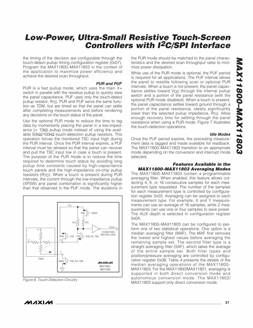
Touch-Detect Modes and OptionsFigure 6 shows the internal circuitry in theMAX11800–MAX11803 used to detect the presence ofa touch on the panel. The selection of the pullup resis-tance value (RTD = touch-detect resistance) and thedurations of the rough pullup interval (PUR = low-impedance pullup) and fine pullup interval (PUF = high-impedance pullup) are user-defined.
The MAX11800–MAX11803 revert to the low-powerpanel setup when placed in touch-detect mode (TDM).Figure 6 shows the active panel drive switches (YMSWand XPSW are omitted for simplicity). TSW is a dedicat-ed pullup switch used in TDM. TSW is also used duringPUF and TDM. XPSW is activated during PUR periods.TDRSEL allows the selection of an internal pullup resis-tor value of either 50kΩ or 100kΩ.
The X and Y touch-screen plates create an open circuitwith no current flow in the panel when the panel is notbeing touched. In this case, TOUCH (see Figure 6) islow. When a touch causes contact between the panel Xand Y plates, a current path is created and TOUCH ispulled high, as long as RPX + RPY (the sum of panelend-to-end resistance) is much lower than RTD. Typicalopen-circuit panel plate resistances range from 200Ωto 1000Ω.
The MAX11800–MAX11803 enter high-impedancepullup mode (50kΩ or 100kΩ) when the panel is notbeing touched. The device is idle in this mode until a
touch is detected. The YMSW and TSW transistors areon, and the XPSW and PSW transistors are off. With notouch present, the Y- input of the TSC is at ground andthe X+ input is at VDD - VTN, where VTN is the thresholdvoltage of the TSW nMOS device. This is a low-powermode in which no current is consumed until a paneltouch occurs. When a touch is present on the panel,the touch-screen controller (TSC) X+ input is pulled lowby the touch panel plate resistance and the YMSW tran-sistor. This causes TOUCH to assume a logic-high andthe devices either issue the TIRQ interrupt for directconversion modes (MAX11800–MAX11803) or beginself-timed scans for autonomous conversion mode(MAX11800/MAX11801).
The value of the user-defined RTD depends on thecharacteristics of the panel. To ensure reliabledetection values, worst-case panel resistance mustbe checked against RTD. The interaction betweenRTD and the panel (or external noise rejecting)capacitance determines how quickly the panel canbe switched from measurement modes back totouch monitoring mode without reporting falsetouches or erroneous tags due to panel settling.
Panel touch status is also required to tag data from acompleted scan and measurement operation. Followingeach scan operation, the panel must be returned toTDM to determine if the panel is still being touched andif the data obtained during the scan operation shouldbe considered valid. This operation is required sincethe panel cannot be monitored for the presence of atouch during the scan and measurement procedure.
The MAX11800–MAX11803 must return to TDM aftercompleting a measurement and making a decision onthe touch status of the panel. The measurement proce-dure is only completed upon resolution of the touch sta-tus and when data is tagged and available forreadback. The characteristics of the return to TDM and
MODE X+ X- Y+ Y- REF+ REF-
X VDD GND ADC_IN U X+ X-Y ADC_IN U VDD GND Y+ Y-Z1 ADC_IN GND VDD U Y+ X-Z2 U GND VDD ADC_IN Y+ X-
PUR VDD (10Ω) U U GND U —
TDM or PUFVDD through
50kΩ or 100kΩU U GND U —
LPM U U U U U —
Table 3. Summary of Physical Panel Settings for Supported Measurement Types
Note: The ADC input is fully differential with the negative input internally connected to GND. The MAX11800–MAX11803 controlaccess to the PUR, PUF, TDM, and LPM, which do not require setup procedures.
U indicates unconnected node.
MA
X1
18
00
–MA
X1
18
03
Low-Power, Ultra-Small Resistive Touch-ScreenControllers with I2C/SPI Interface
______________________________________________________________________________________ 21
the timing of the decision are configurable through thetouch-detect pullup timing configuration register (0x07).Program the MAX11800–MAX11803 in the context ofthe application to maximize power efficiency andachieve the desired scan throughput.
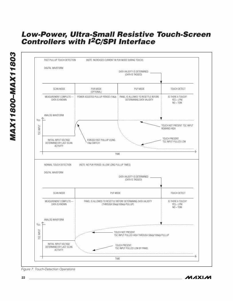
PUR and PUFPUR is a fast pullup mode, which uses the main X+switch in parallel with the resistive pullup to quickly slewthe panel capacitance. PUF uses only the touch-detectpullup resistor, RTD. PUR and PUF serve the same func-tion as TDM, but are timed so that the panel can settleafter completing measurements and before renderingany decisions on the touch status of the panel.
Use the optional PUR mode to reduce the time to tagdata by momentarily placing the panel in a low-imped-ance (< 10Ω) pullup mode instead of using the avail-able 50kΩ/100kΩ touch-detection pullup resistors. Thisoperation forces the monitored TSC input high duringthe PUR interval. Once the PUR interval expires, a PUFinterval must be allowed so that the panel can recoverand pull the TSC input low in case a touch is present.The purpose of the PUR mode is to reduce the timerequired to determine touch status by avoiding longpullup time constants caused by high-capacitancetouch panels and the high-impedance on-chip pullupresistors (RTD). When a touch is present during PURintervals, the current through the low-impedance pullup(XPSW) and panel combination is significantly higherthan that observed in the PUF mode. The durations in
the PUR mode should be matched to the panel charac-teristics and the desired scan throughput rates to mini-mize power dissipation.
While use of the PUR mode is optional, the PUF periodis required for all applications. The PUF interval allowsthe panel to resettle following scan or optional PURintervals. When a touch is not present, the panel capac-itance settles toward VDD through the internal pullupswitch and a portion of the panel resistance (with theoptional PUR mode disabled). When a touch is present,the panel capacitance settles toward ground through aportion of the panel resistance, ideally significantlylower than the selected pullup impedance, RTD. Allowenough recovery time for settling through the panelresistance when using a PUR mode. Figure 7 illustratesthe touch-detection operations.
Idle ModesOnce the PUF period expires, the preceding measure-ment data is tagged and made available for readback.The MAX11800–MAX11803 transition to an appropriatemode depending on the conversion and interrupt modeselected.
Features Available in theMAX11800–MAX11803 Averaging Modes
The MAX11800–MAX11803 contain a programmableaveraging filter. When enabled, this feature allows col-lecting 4, 8, or 16 consecutive samples for each mea-surement type requested. The number of the samplesfor each measurement type is controlled by configura-tion register 0x03. Averaging can be assigned to eachmeasurement type. For example, X and Y measure-ments can use an average of 16 samples, while Z mea-surements can use one or four samples to save power.The AUX depth is selected in configuration register0x0A.
The MAX11800–MAX11803 can be configured to per-form one of two statistical operations. One option is amedian averaging filter (MAF). The MAF first removesthe lowest and highest values before averaging theremaining sample set. The second filter type is astraight averaging filter (SAF), which takes the averageof the entire sample set. Both f i l ter types andposition/pressure averaging are controlled by configu-ration register 0x0B. Table 4 presents the details of themedian averaging operations of the MAX11800–MAX11803. For the MAX11800/MAX11801, averaging issupported in both direct conversion mode andautonomous conversion mode. The MAX11802/MAX11803 support only direct conversion mode.
MAX11800–MAX11803
PUR, PUF, TDM
PUR
VDD
YMSW
XPSW
TDRSELPSW
PANEL
TSW
RTD RTD
Y-
X+
PUR, PUF, TDM
(TO MAX11800/MAX11801 LOGIC)
Y+
X-
TOUCH
Figure 6. Touch-Detection Circuitry
MA
X1
18
00
–MA
X1
18
03
Low-Power, Ultra-Small Resistive Touch-ScreenControllers with I2C/SPI Interface
22 ______________________________________________________________________________________
TOUCH DETECTPUR MODE(OPTIONAL)
PUF MODESCAN MODE
MEASUREMENT COMPLETE—DATA IS KNOWN
POWER ASSISTED PULLUP PERIOD (10Ω) PANEL IS ALLOWED TO RESETTLE BEFOREDETERMINING DATA VALIDITY
IS THERE A TOUCH?YES = LPM.NO = TDM.
MEASUREMENT COMPLETE—DATA IS KNOWN
PANEL IS ALLOWED TO RESETTLE BEFORE DETERMINING DATA VALIDITY(THROUGH 50kΩ/100kΩ PULLUP)
IS THERE A TOUCH?YES = LPM.NO = TDM.
DATA VALIDITY IS DETERMINED(DATA IS TAGGED)
DATA VALIDITY IS DETERMINED(DATA IS TAGGED)
INITIAL INPUT VOLTAGEDETERMINED BY LAST SCAN
ACTIVITY
INITIAL INPUT VOLTAGEDETERMINED BY LAST SCAN
ACTIVITY
FORCED FAST PULLUP USING10Ω SWITCH
TOUCH NOT PRESENT: TSC INPUTREMAINS HIGH
TOUCH PRESENT:TSC INPUT PULLED LOW
TOUCH NOT PRESENT:TSC INPUT PULLED HIGH THROUGH 50kΩ/100kΩ PULLUP
TOUCH PRESENT:TSC INPUT PULLED LOW BY PANEL
TIME
TSC
INPU
T
DIGITAL WAVEFORM
ANALOG WAVEFORM
TIME
DIGITAL WAVEFORM
ANALOG WAVEFORM
NORMAL TOUCH DETECTION (NOTE: NO PUR PERIOD; ALLOW LONG PULLUP TIMES)
FAST PULLUP TOUCH DETECTION (NOTE: INCREASED CURRENT IN PUR MODE DURING TOUCH)
VDD
TSC
INPU
T
VDD
TOUCH DETECTPUF MODESCAN MODE
Figure 7. Touch-Detection Operations
MA
X1
18
00
–MA
X1
18
03
Low-Power, Ultra-Small Resistive Touch-ScreenControllers with I2C/SPI Interface
______________________________________________________________________________________ 23
Combined CommandsCombined commands reduce AP interaction with theMAX11800–MAX11803 by allowing multiple measure-ments. For example, the MAX11800–MAX11803 can beinstructed to provide X and Y data, or X and Y and Z1data, or X and Y and Z1 and Z2 data using a singlecommand.
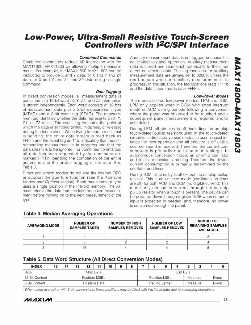
Data TaggingIn direct conversion modes, all measurement data iscontained in a 16-bit word. X, Y, Z1, and Z2 informationis stored independently. Each word consists of 12 bitsof measurement data plus a 2-bit measurement type(MTAG) and a 2-bit event tag (ETAG). The measure-ment tag identifies whether the data represents an X, Y,Z1, or Z2 result. The event tag indicates the point atwhich the data is sampled (initial, midpress, or release)during the touch event. When trying to read a result thatis pending, the entire data stream is read back asFFFFh and the event tag as 11b, indicating that the cor-responding measurement is in progress and that thedata stream is to be ignored. For combined commands,all data locations requested by the command aremarked FFFFh, pending the completion of the entirecommand and the proper tagging of the data. SeeTable 5.
Direct conversion modes do not use the internal FIFOor support the aperture function (see the ApertureModes and Options section). Each measurement typeuses a single location in the (16-bit) memory. The APmust retrieve the data from the last requested measure-ment before moving on to the next measurement of thetype.
Auxiliary measurement data is not tagged because it isnot related to panel operation. Auxiliary measurementdata is stored and read back identically to the otherdirect conversion data. The tag locations for auxiliarymeasurement data are always set to 0000b, unless theread occurs when an auxiliary measurement is inprogress. In this situation, the tag locations read 1111band the data stream reads back FFFFh.
Low-Power ModesThere are also two low-power modes, LPM and TDM.LPM only applies when in DCM with edge interruptmode or ACM during periods following a conversionwhere the panel was observed to be touched and asubsequent panel measurement is required and/orscheduled.
During LPM, all circuitry is off, including the on-chiptouch-detect pullup resistors used in the touch-detectcircuitry. In direct conversion modes, a user-request ini-tiates the next operation and all circuitry is off until auser-command is received. Therefore, the current con-sumption is primarily due to junction leakage. Inautonomous conversion mode, an on-chip oscillatorand timer are constantly running. Therefore, the devicecurrent consumption is primarily determined by theoscillator and timer.
During TDM, all circuitry is off except the on-chip pullupresistor. This is an untimed mode (oscillator and timerare off) for both ACM and DCM (no digital current). Thismode only consumes current through the on-chippullup resistor when a touch is present. The device canbe powered down through register 0x0B when no panelinput is expected or needed, and, therefore, no poweris consumed through the panel.
INDEX 15 14 13 12 11 10 9 8 7 6 5 4 3 2 1 0
Byte MSB Byte LSB Byte
12-Bit Content Position MSBs Position LSBs Measure Event
8-Bit Content Position Data Trailing Zeros* Measure Event
Table 5. Data Word Structure (All Direct Conversion Modes)
AVERAGING MODENUMBER OF
SAMPLES TAKENNUMBER OF HIGH
SAMPLES REMOVEDNUMBER OF LOW
SAMPLES REMOVED
NUMBER OFREMAINING SAMPLES
AVERAGED
1 4 1 1 2
2 8 2 2 4
3 16 4 4 8
Table 4. Median Averaging Operations
*When using averaging with 8-bit conversions, these positions may be filled with fractional data due to averaging operations.
MA
X1
18
00
–MA
X1
18
03
Low-Power, Ultra-Small Resistive Touch-ScreenControllers with I2C/SPI Interface
24 ______________________________________________________________________________________
Features Available in theMAX11800/MAX11801 Only
Autonomous ModeThe MAX11800/MAX11801 can perform measurementsautomatically without the AP involvement, and isreferred to as autonomous conversion mode (ACM).When operating in ACM, the MAX11800/MAX11801 usean on-chip FIFO to store measurement results. As eachnew data is written to the FIFO, an interrupt is generat-ed. The AP can choose to service (read) the FIFO resultafter each interrupt or wait until the FIFO is full thenread the entire FIFO contents at once. The AP can alsoread the contents of the FIFO at any time. See theAutonomous Conversion Mode section for a furtherdescription of operations.
ApertureThe MAX11800/MAX11801 contain a feature referred toas aperture. It is only available on the MAX11800/MAX11801 when operating in autonomous conversionmode. The aperture feature creates an invisible rectan-gle around a touch location within the MAX11800/MAX11801 hardware. The size of the rectangle is userprogrammable. One application of the aperture featureis to provide “spatial hysteresis.” Spatial hysteresis canbe useful for applications that require lower resolutiontouch accuracy without requiring the AP to handle themathematics involved to filter out extraneous data.Another application would be to use the aperture fea-ture to implement simple single finger or stylus ges-tures. See the Using Aperture Mode section for afurther description of operations.
Panel Setup, Measurement, and Scan CommandsTo simplify measurement procedures, the MAX11800–MAX11803 support three types of commands: panelsetup commands (PSU), panel measurement commands(PMC), and combined measurement commands (CMC).
In direct conversion mode, the MAX11800/MAX11801can use all three types of commands. Using individualpanel setup and measurement commands allow for ahigh degree of customization based on decisions madeby the AP, while using combined commands signifi-cantly simplifies the complete measurement processand reduces communications between the AP and theMAX11800–MAX11803.
In autonomous mode, the MAX11800/MAX11801 usecombined commands to control and automate allaspects of panel setup, measurements, and timing. Seethe Operating Mode Configuration Register (0x0B) sec-tion for more details.
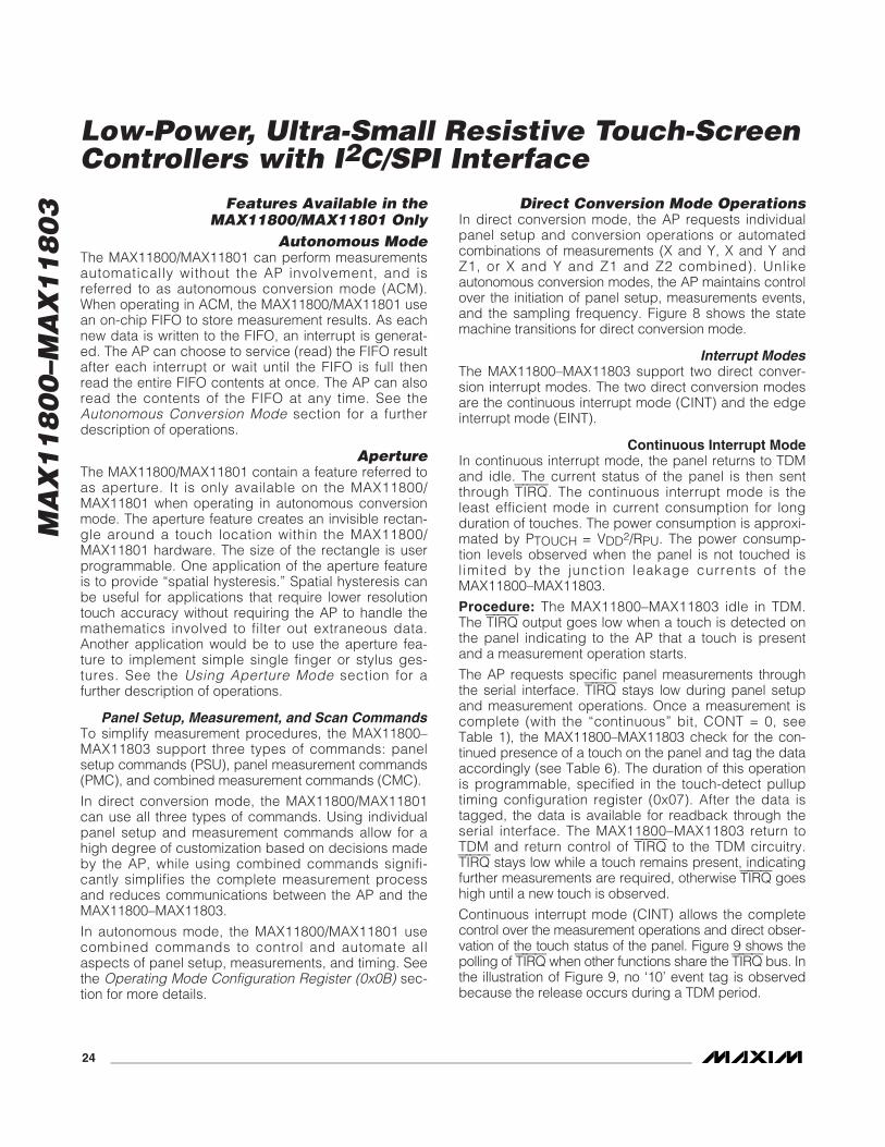
Direct Conversion Mode OperationsIn direct conversion mode, the AP requests individualpanel setup and conversion operations or automatedcombinations of measurements (X and Y, X and Y andZ1, or X and Y and Z1 and Z2 combined). Unlikeautonomous conversion modes, the AP maintains controlover the initiation of panel setup, measurements events,and the sampling frequency. Figure 8 shows the statemachine transitions for direct conversion mode.
Interrupt ModesThe MAX11800–MAX11803 support two direct conver-sion interrupt modes. The two direct conversion modesare the continuous interrupt mode (CINT) and the edgeinterrupt mode (EINT).
Continuous Interrupt ModeIn continuous interrupt mode, the panel returns to TDMand idle. The current status of the panel is then sentthrough TIRQ. The continuous interrupt mode is theleast efficient mode in current consumption for longduration of touches. The power consumption is approxi-mated by PTOUCH = VDD2/RPU. The power consump-tion levels observed when the panel is not touched isl imited by the junction leakage currents of theMAX11800–MAX11803.
Procedure: The MAX11800–MAX11803 idle in TDM.The TIRQ output goes low when a touch is detected onthe panel indicating to the AP that a touch is presentand a measurement operation starts.
The AP requests specific panel measurements throughthe serial interface. TIRQ stays low during panel setupand measurement operations. Once a measurement iscomplete (with the “continuous” bit, CONT = 0, seeTable 1), the MAX11800–MAX11803 check for the con-tinued presence of a touch on the panel and tag the dataaccordingly (see Table 6). The duration of this operationis programmable, specified in the touch-detect pulluptiming configuration register (0x07). After the data istagged, the data is available for readback through theserial interface. The MAX11800–MAX11803 return toTDM and return control of TIRQ to the TDM circuitry.TIRQ stays low while a touch remains present, indicatingfurther measurements are required, otherwise TIRQ goeshigh until a new touch is observed.
Continuous interrupt mode (CINT) allows the completecontrol over the measurement operations and direct obser-vation of the touch status of the panel. Figure 9 shows thepolling of TIRQ when other functions share the TIRQ bus. Inthe illustration of Figure 9, no ‘10’ event tag is observedbecause the release occurs during a TDM period.
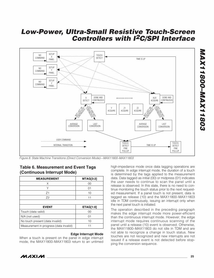
Edge Interrupt ModeWhen a touch is present on the panel in edge interruptmode, the MAX11800–MAX11803 return to an untimed
high-impedance mode once data tagging operations arecomplete. In edge interrupt mode, the duration of a touchis determined by the tags applied to the measurementdata. Data tagged as initial (00) or midpress (01) indicatesthe user needs to continue to scan the panel until arelease is observed. In this state, there is no need to con-tinue monitoring the touch status prior to the next request-ed measurement. If a panel touch is not present, data istagged as release (10) and the MAX11800–MAX11803idle in TDM continuously, issuing an interrupt only whenthe next panel touch is initiated.
The operation described in the preceding paragraphmakes the edge interrupt mode more power-efficientthan the continuous interrupt mode. However, the edgeinterrupt mode requires continuous scanning of thepanel until a release (10) event is observed. Otherwise,the MAX11800–MAX11803 do not idle in TDM and arenot able to recognize a change in touch status. Newtouches are not recognized and new interrupts are notissued if a release event is not detected before stop-ping the conversion sequence.
MA
X1
18
00
–MA
X1
18
03
Low-Power, Ultra-Small Resistive Touch-ScreenControllers with I2C/SPI Interface
______________________________________________________________________________________ 25
Z1ACQUIRE
Z2ACQUIRE
TOUCHDETECT
TOUCH-DETECT
FINEPULLUP
TOUCH-DETECT
FINEPULLUP
TIME IS UP
SETUPX
PANEL
YACQUIRE
XDETECT
AUXACQUIRE
AVERAGECONVERSION
LASTCONVERSION
NOT LAS
T OR
CONTINUOUS
LAST AND NOT
CONTINUOUS NOT LAS
T OR
CONTINUOUS
LAST AND NOT
CONTINUOUS
TIME IS UP
DONE ANDCONTINUOUS
DONE ANDCONTINUOUS
AVERAGECONVERSION
LASTCONVERSION
NOCOMMAND
NOCOMMAND
NOCOMMAND
USER COMMAND
INTERNAL TRANSITION
SETUPY
PANEL
SETUPZ
PANEL
Figure 8. State Machine Transitions (Direct Conversion Mode)—MAX11800–MAX11803
MEASUREMENT MTAG[3:2]
X 00
Y 01
Z1 10
Z2 11
EVENT ETAG[1:0]
Touch (data valid) 00
N/A (not used) 01
No touch present (data invalid) 10
Measurement in progress (data invalid) 11
Table 6. Measurement and Event Tags(Continuous Interrupt Mode)
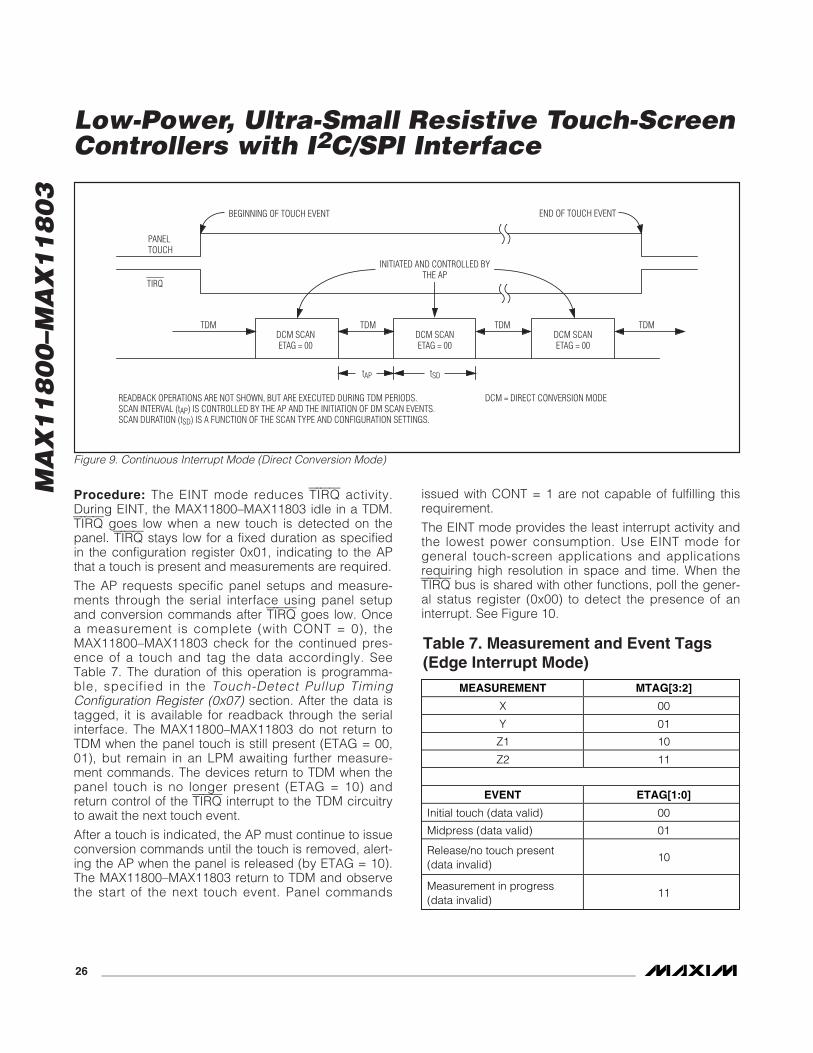
MA
X1
18
00
–MA
X1
18
03
Low-Power, Ultra-Small Resistive Touch-ScreenControllers with I2C/SPI Interface
26 ______________________________________________________________________________________
Procedure: The EINT mode reduces TIRQ activity.During EINT, the MAX11800–MAX11803 idle in a TDM.TIRQ goes low when a new touch is detected on thepanel. TIRQ stays low for a fixed duration as specifiedin the configuration register 0x01, indicating to the APthat a touch is present and measurements are required.
The AP requests specific panel setups and measure-ments through the serial interface using panel setupand conversion commands after TIRQ goes low. Oncea measurement is complete (with CONT = 0), theMAX11800–MAX11803 check for the continued pres-ence of a touch and tag the data accordingly. SeeTable 7. The duration of this operation is programma-ble, specified in the Touch-Detect Pullup TimingConfiguration Register (0x07) section. After the data istagged, it is available for readback through the serialinterface. The MAX11800–MAX11803 do not return toTDM when the panel touch is still present (ETAG = 00,01), but remain in an LPM awaiting further measure-ment commands. The devices return to TDM when thepanel touch is no longer present (ETAG = 10) andreturn control of the TIRQ interrupt to the TDM circuitryto await the next touch event.
After a touch is indicated, the AP must continue to issueconversion commands until the touch is removed, alert-ing the AP when the panel is released (by ETAG = 10).The MAX11800–MAX11803 return to TDM and observethe start of the next touch event. Panel commands
issued with CONT = 1 are not capable of fulfilling thisrequirement.
The EINT mode provides the least interrupt activity andthe lowest power consumption. Use EINT mode forgeneral touch-screen applications and applicationsrequiring high resolution in space and time. When theTIRQ bus is shared with other functions, poll the gener-al status register (0x00) to detect the presence of aninterrupt. See Figure 10.
MEASUREMENT MTAG[3:2]
X 00
Y 01
Z1 10
Z2 11
EVENT ETAG[1:0]
Initial touch (data valid) 00
Midpress (data valid) 01
Release/no touch present(data invalid)
10
Measurement in progress(data invalid)
11
Table 7. Measurement and Event Tags(Edge Interrupt Mode)
DCM SCANETAG = 00
DCM SCANETAG = 00
DCM SCANETAG = 00
TDM TDM TDM TDM
TIRQ
PANELTOUCH
BEGINNING OF TOUCH EVENT END OF TOUCH EVENT
tAP tSD
READBACK OPERATIONS ARE NOT SHOWN, BUT ARE EXECUTED DURING TDM PERIODS.SCAN INTERVAL (tAP) IS CONTROLLED BY THE AP AND THE INITIATION OF DM SCAN EVENTS.SCAN DURATION (tSD) IS A FUNCTION OF THE SCAN TYPE AND CONFIGURATION SETTINGS.
DCM = DIRECT CONVERSION MODE
INITIATED AND CONTROLLED BYTHE AP
Figure 9. Continuous Interrupt Mode (Direct Conversion Mode)
MA
X1
18
00
–MA
X1
18
03
Low-Power, Ultra-Small Resistive Touch-ScreenControllers with I2C/SPI Interface
______________________________________________________________________________________ 27
Panel Setup Commands Panel setup commands configure the touch panel prior toa measurement. Panel setup commands allow the panelto fully settle before performing a measurement. Thepanel setup command summary is shown in Table 8. Seethe register map in the Status and Configuration Registerssection for details on the panel setup timing options for X,Y, Z1, and Z2 measurements.
The continuation bit (CONT) of the panel setup com-mand programs the MAX11800–MAX11803 to maintainthe present panel setting at the end of the command(CONT = 1). Panel setup commands assume a logicalprogression to an appropriate measurement. For exam-ple, when the MAX11800–MAX11803 are in the X panelsetup mode, the devices can proceed to an X measure-ment mode only. The devices return to LPM when anincompatible command follows a panel setup com-mand. See Figure 11. For most applications adequatetime for panel setup is available as an integral part of
the panel measurement commands; configured usingthe panel setup timing configuration register, 0x05. Thededicated panel setup commands are primarily provid-ed to support applications where the AP needs to con-trol panel setup directly or long panel setup time isrequired.
Panel Measurement CommandsA measurement command selects one of the four phys-ical setup options: X, Y, Z1, or Z2.
All panel measurement commands include timed inter-vals to power up both the internal ADC and the panelwith programmable durations. The delayed conversiontime (tD_CV, delayed conversion configuration register(0x06)) governs the time that the panel and the ADCneed to settle prior to the initiations of conversions. Theminimum delayed conversion time is 10μs, which is thetime the internal ADC needs to power up. If more set-tling time is required, increase the panel settling time
HEX ACCESS PAIRABLE COMMAND LENGTH OPERATION
0x69h Write No 8 X = panel setup
0x6Bh Write No 8 Y = panel setup
0x6Dh Write No 8 Z1 = panel setup
0x6Fh Write No 8 Z2 = panel setup
Table 8. Panel Setup Command Summary
DCM SCANETAG = 10
DCM SCANETAG = 01
DCM SCANETAG = 00
TDM LPM LPM TDM
TIRQ
PANELTOUCH
BEGINNING OF TOUCH EVENT END OF TOUCH EVENT
tAP tSD
READBACK OPERATIONS ARE NOT SHOWN, BUT ARE EXECUTED DURING TDM PERIODS.TIRQ DURATION (tIRQ) IS SPECIFIED BY THE GENERAL CONFIGURATION REGISTER (0x01).SCAN INTERVAL (tAP) IS CONTROLLED BY THE AP AND THE INITIATION OF DM SCAN EVENTS.SCAN DURATION (tSD) IS A FUNCTION OF THE SCAN TYPE AND CONFIGURATION SETTINGS.
tIRQ INITIATED AND CONTROLLED BYTHE AP
DCM = DIRECT CONVERSION MODE
Figure 10. Edge Interrupt Mode (Direct Conversion Mode)—MAX11800–MAX11803
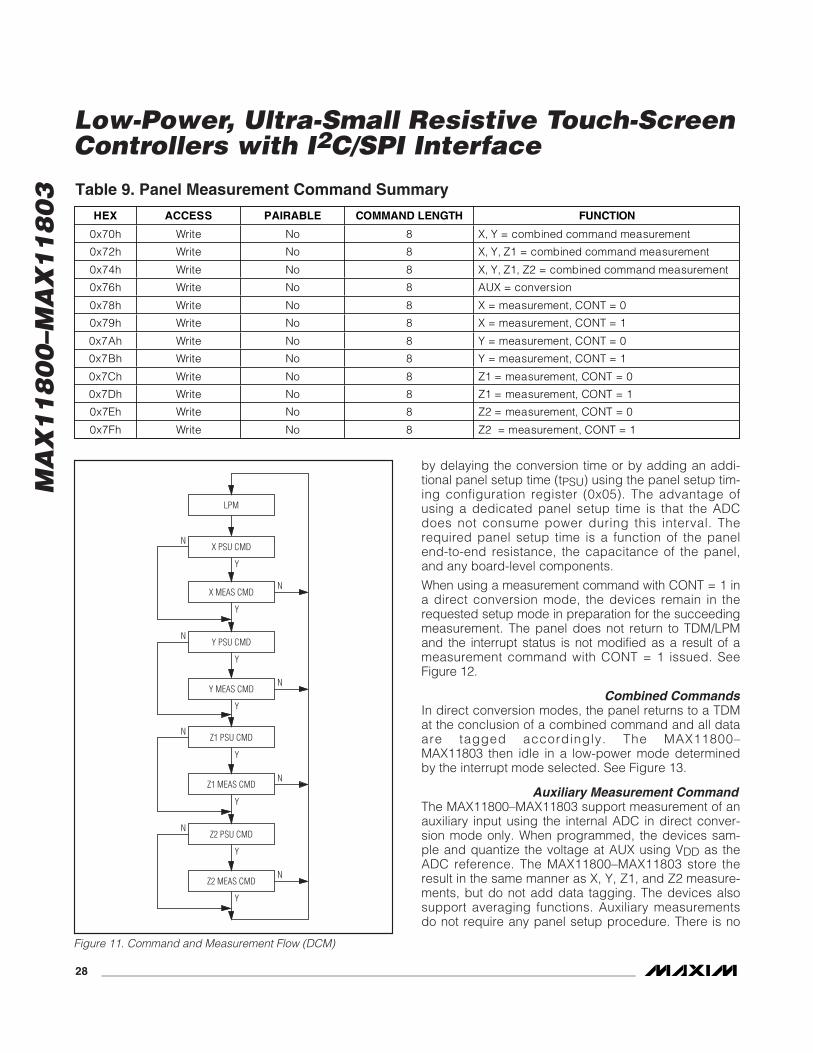
MA
X1
18
00
–MA
X1
18
03
Low-Power, Ultra-Small Resistive Touch-ScreenControllers with I2C/SPI Interface
28 ______________________________________________________________________________________
by delaying the conversion time or by adding an addi-tional panel setup time (tPSU) using the panel setup tim-ing configuration register (0x05). The advantage ofusing a dedicated panel setup time is that the ADCdoes not consume power during this interval. Therequired panel setup time is a function of the panelend-to-end resistance, the capacitance of the panel,and any board-level components.
When using a measurement command with CONT = 1 ina direct conversion mode, the devices remain in therequested setup mode in preparation for the succeedingmeasurement. The panel does not return to TDM/LPMand the interrupt status is not modified as a result of ameasurement command with CONT = 1 issued. SeeFigure 12.
Combined Commands In direct conversion modes, the panel returns to a TDMat the conclusion of a combined command and all dataare tagged accordingly. The MAX11800–MAX11803 then idle in a low-power mode determinedby the interrupt mode selected. See Figure 13.
Auxiliary Measurement CommandThe MAX11800–MAX11803 support measurement of anauxiliary input using the internal ADC in direct conver-sion mode only. When programmed, the devices sam-ple and quantize the voltage at AUX using VDD as theADC reference. The MAX11800–MAX11803 store theresult in the same manner as X, Y, Z1, and Z2 measure-ments, but do not add data tagging. The devices alsosupport averaging functions. Auxiliary measurementsdo not require any panel setup procedure. There is no
HEX ACCESS PAIRABLE COMMAND LENGTH FUNCTION
0x70h Write No 8 X, Y = combined command measurement
0x72h Write No 8 X, Y, Z1 = combined command measurement
0x74h Write No 8 X, Y, Z1, Z2 = combined command measurement
0x76h Write No 8 AUX = conversion
0x78h Write No 8 X = measurement, CONT = 0
0x79h Write No 8 X = measurement, CONT = 1
0x7Ah Write No 8 Y = measurement, CONT = 0
0x7Bh Write No 8 Y = measurement, CONT = 1
0x7Ch Write No 8 Z1 = measurement, CONT = 0
0x7Dh Write No 8 Z1 = measurement, CONT = 1
0x7Eh Write No 8 Z2 = measurement, CONT = 0
0x7Fh Write No 8 Z2 = measurement, CONT = 1
Table 9. Panel Measurement Command Summary
LPM
X PSU CMD
X MEAS CMDN
Y PSU CMD
Y MEAS CMD
Z1 PSU CMD
Z1 MEAS CMD
Z2 PSU CMD
Z2 MEAS CMD
Y
N
Y
N
Y
N
Y
N
Y
N
Y
N
Y
N
Y
Figure 11. Command and Measurement Flow (DCM)
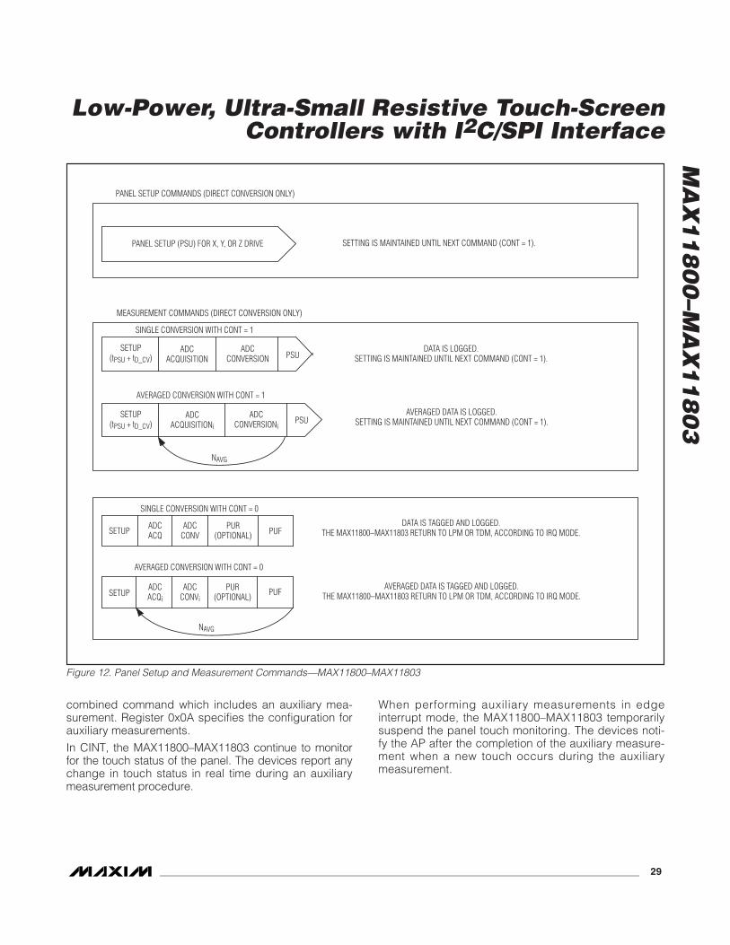
MA
X1
18
00
–MA
X1
18
03
Low-Power, Ultra-Small Resistive Touch-ScreenControllers with I2C/SPI Interface
______________________________________________________________________________________ 29
PANEL SETUP (PSU) FOR X, Y, OR Z DRIVE SETTING IS MAINTAINED UNTIL NEXT COMMAND (CONT = 1).
PANEL SETUP COMMANDS (DIRECT CONVERSION ONLY)
MEASUREMENT COMMANDS (DIRECT CONVERSION ONLY)
SINGLE CONVERSION WITH CONT = 1
SINGLE CONVERSION WITH CONT = 0
AVERAGED CONVERSION WITH CONT = 0
SETUP(tPSU + tD_CV)
ADCACQUISITION
ADCCONVERSION
ADCACQUISITIONi
ADCCONVERSIONi
PSUDATA IS LOGGED.
SETTING IS MAINTAINED UNTIL NEXT COMMAND (CONT = 1).
AVERAGED CONVERSION WITH CONT = 1
SETUP(tPSU + tD_CV) PSU
AVERAGED DATA IS LOGGED.SETTING IS MAINTAINED UNTIL NEXT COMMAND (CONT = 1).
DATA IS TAGGED AND LOGGED.THE MAX11800–MAX11803 RETURN TO LPM OR TDM, ACCORDING TO IRQ MODE.
AVERAGED DATA IS TAGGED AND LOGGED.THE MAX11800–MAX11803 RETURN TO LPM OR TDM, ACCORDING TO IRQ MODE.
NAVG
NAVG
SETUPADCACQ
ADCCONV
PUR(OPTIONAL)
ADCACQi
ADCCONVi
PUR(OPTIONAL)
PUF
SETUP PUF
Figure 12. Panel Setup and Measurement Commands—MAX11800–MAX11803
combined command which includes an auxiliary mea-surement. Register 0x0A specifies the configuration forauxiliary measurements.
In CINT, the MAX11800–MAX11803 continue to monitorfor the touch status of the panel. The devices report anychange in touch status in real time during an auxiliarymeasurement procedure.
When performing auxiliary measurements in edgeinterrupt mode, the MAX11800–MAX11803 temporarilysuspend the panel touch monitoring. The devices noti-fy the AP after the completion of the auxiliary measure-ment when a new touch occurs during the auxiliarymeasurement.
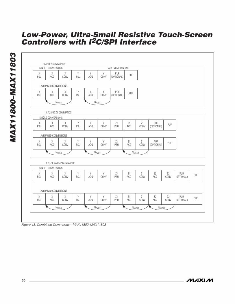
MA
X1
18
00
–MA
X1
18
03
Low-Power, Ultra-Small Resistive Touch-ScreenControllers with I2C/SPI Interface
30 ______________________________________________________________________________________
X AND Y COMMANDSSINGLE CONVERSIONS DATA EVENT TAGGING
AVERAGED CONVERSIONS
XPSU
XACQ
XCONV
YPSU
YACQ
YCONV
PUR(OPTIONAL) PUF
XPSU
XACQ
XCONV
YPSU
YACQ
YCONV
PUR(OPTIONAL) PUF
X, Y, AND Z1 COMMANDS
NAVGX NAVGY
SINGLE CONVERSIONS
AVERAGED CONVERSIONS
XPSU
XACQ
XCONV
YPSU
YACQ
Z1CONV
PUR(OPTIONAL) PUF
XPSU
XACQ
XCONV
YPSU
YACQ
YCONV
Z1PSU
Z1ACQ
YCONV
Z1PSU
Z1ACQ
Z1CONV
PUR(OPTIONAL) PUF
NAVGZ1
X, Y, Z1, AND Z2 COMMANDS
SINGLE CONVERSIONS
AVERAGED CONVERSIONS
XPSU
XACQ
XCONV
YPSU
YACQ
Z1CONV
PUR(OPTIONAL) PUF
XPSU
XACQ
XCONV
YPSU
YACQ
YCONV
Z1PSU
Z1ACQ
YCONV
Z1PSU
Z1ACQ
Z1CONV
Z2CONV
Z2ACQ
Z2ACQ
Z2CONV
PUR(OPTIONAL) PUF
NAVGZ2
NAVGX NAVGY
NAVGZ1NAVGX NAVGY
Figure 13. Combined Commands—MAX11800–MAX11803
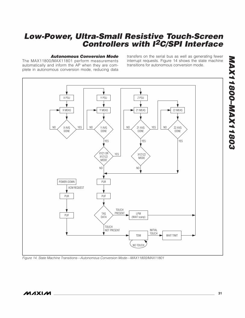
MA
X1
18
00
–MA
X1
18
03
Low-Power, Ultra-Small Resistive Touch-ScreenControllers with I2C/SPI Interface
______________________________________________________________________________________ 31
X AVGDONE
X MEAS
YESNO
NO
XYZ1 ORXYZ1Z2MODE
YES
POWER-DOWN
LPM(WAIT scanp)
X PSU
Y AVGDONE
Y MEAS
YES
YES
NO
TAGDATA
TDM
NO TOUCH
WAIT TINIT
PUR
PUF
TOUCHPRESENT
ACM REQUEST
INITIALTOUCH
TOUCHNOT PRESENT
PUR
PUF
Y PSU
Z2 AVGDONE
Z2 MEAS
NO
NO
XYZ1Z2MODE
Z1 AVGDONE
Z1 MEAS
YES
NO
YES
Z PSU
Figure 14. State Machine Transitions––Autonomous Conversion Mode—MAX11800/MAX11801
Autonomous Conversion ModeThe MAX11800/MAX11801 perform measurementsautomatically and inform the AP when they are com-plete in autonomous conversion mode, reducing data
transfers on the serial bus as well as generating fewerinterrupt requests. Figure 14 shows the state machinetransitions for autonomous conversion mode.
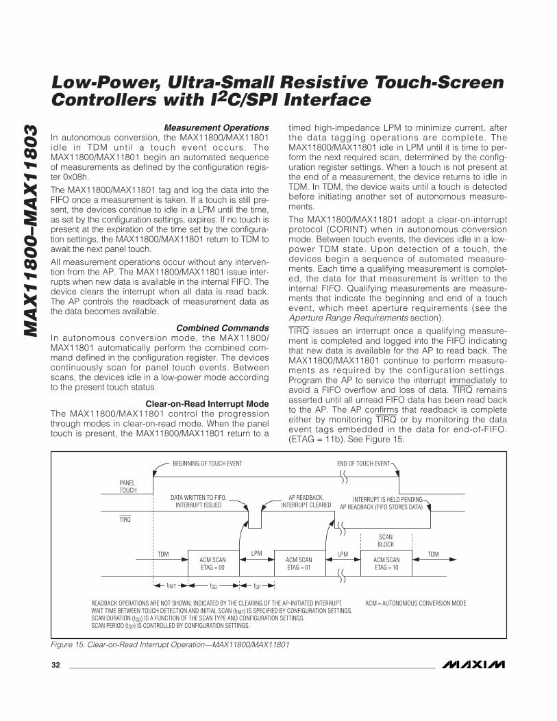
MA
X1
18
00
–MA
X1
18
03
Low-Power, Ultra-Small Resistive Touch-ScreenControllers with I2C/SPI Interface
32 ______________________________________________________________________________________
TDM LPM TDM
TIRQ
PANELTOUCH
END OF TOUCH EVENTBEGINNING OF TOUCH EVENT
tSPtSD
LPM
INTERRUPT IS HELD PENDINGAP READBACK (FIFO STORES DATA)
AP READBACK,INTERRUPT CLEARED
DATA WRITTEN TO FIFO,INTERRUPT ISSUED
tINIT
SCANBLOCK
ACM SCANETAG = 00
ACM SCANETAG = 01
ACM SCANETAG = 10
READBACK OPERATIONS ARE NOT SHOWN, INDICATED BY THE CLEARING OF THE AP-INITIATED INTERRUPT.WAIT TIME BETWEEN TOUCH DETECTION AND INITIAL SCAN (tINIT) IS SPECIFIED BY CONFIGURATION SETTINGS.SCAN DURATION (tSD) IS A FUNCTION OF THE SCAN TYPE AND CONFIGURATION SETTINGS.SCAN PERIOD (tSP) IS CONTROLLED BY CONFIGURATION SETTINGS.
ACM = AUTONOMOUS CONVERSION MODE
Figure 15. Clear-on-Read Interrupt Operation—MAX11800/MAX11801
Measurement Operations In autonomous conversion, the MAX11800/MAX11801idle in TDM unti l a touch event occurs. TheMAX11800/MAX11801 begin an automated sequenceof measurements as defined by the configuration regis-ter 0x08h.
The MAX11800/MAX11801 tag and log the data into theFIFO once a measurement is taken. If a touch is still pre-sent, the devices continue to idle in a LPM until the time,as set by the configuration settings, expires. If no touch ispresent at the expiration of the time set by the configura-tion settings, the MAX11800/MAX11801 return to TDM toawait the next panel touch.
All measurement operations occur without any interven-tion from the AP. The MAX11800/MAX11801 issue inter-rupts when new data is available in the internal FIFO. Thedevice clears the interrupt when all data is read back.The AP controls the readback of measurement data asthe data becomes available.
Combined Commands In autonomous conversion mode, the MAX11800/MAX11801 automatically perform the combined com-mand defined in the configuration register. The devicescontinuously scan for panel touch events. Betweenscans, the devices idle in a low-power mode accordingto the present touch status.
Clear-on-Read Interrupt Mode The MAX11800/MAX11801 control the progressionthrough modes in clear-on-read mode. When the paneltouch is present, the MAX11800/MAX11801 return to a
timed high-impedance LPM to minimize current, afterthe data tagging operations are complete. TheMAX11800/MAX11801 idle in LPM until it is time to per-form the next required scan, determined by the config-uration register settings. When a touch is not present atthe end of a measurement, the device returns to idle inTDM. In TDM, the device waits until a touch is detectedbefore initiating another set of autonomous measure-ments.
The MAX11800/MAX11801 adopt a clear-on-interruptprotocol (CORINT) when in autonomous conversionmode. Between touch events, the devices idle in a low-power TDM state. Upon detection of a touch, thedevices begin a sequence of automated measure-ments. Each time a qualifying measurement is complet-ed, the data for that measurement is written to theinternal FIFO. Qualifying measurements are measure-ments that indicate the beginning and end of a touchevent, which meet aperture requirements (see theAperture Range Requirements section).
TIRQ issues an interrupt once a qualifying measure-ment is completed and logged into the FIFO indicatingthat new data is available for the AP to read back. TheMAX11800/MAX11801 continue to perform measure-ments as required by the configuration settings.Program the AP to service the interrupt immediately toavoid a FIFO overflow and loss of data. TIRQ remainsasserted until all unread FIFO data has been read backto the AP. The AP confirms that readback is completeeither by monitoring TIRQ or by monitoring the dataevent tags embedded in the data for end-of-FIFO.(ETAG = 11b). See Figure 15.
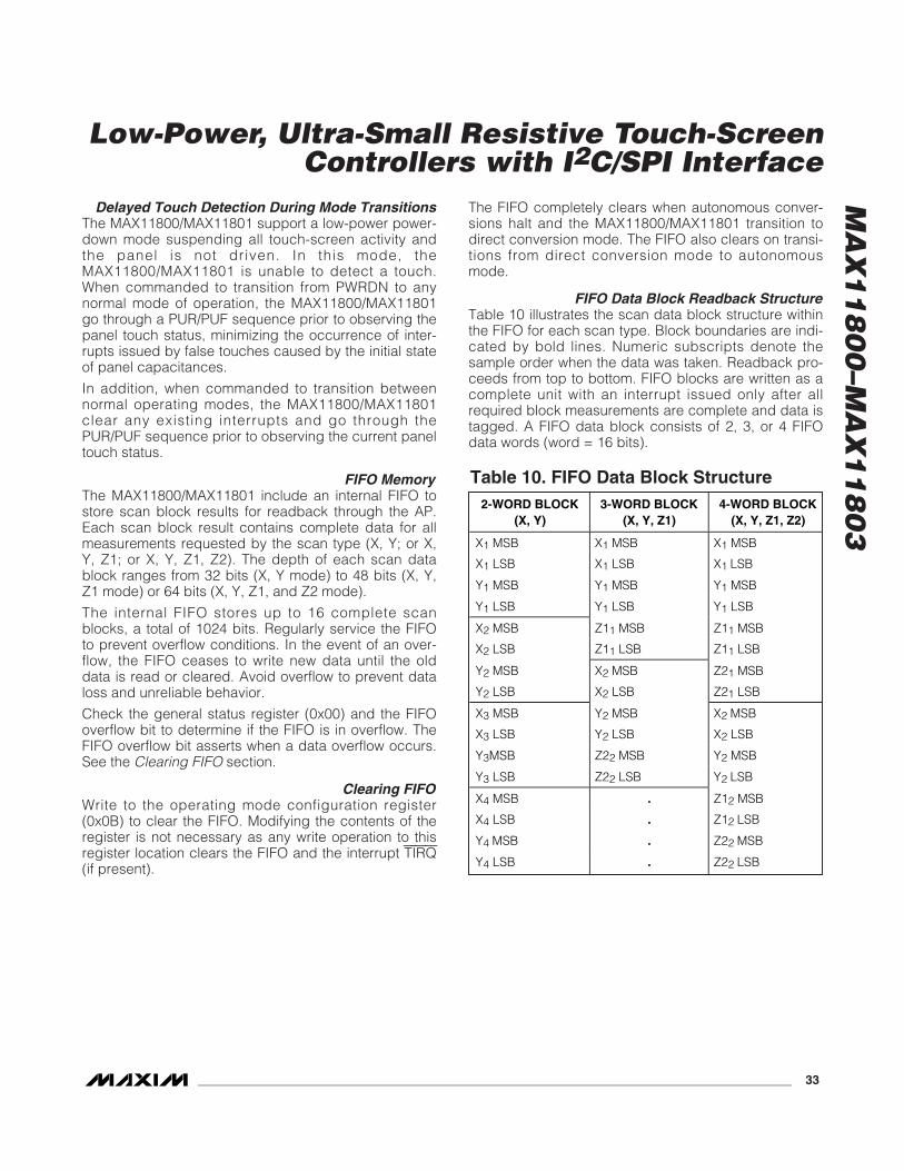
MA
X1
18
00
–MA
X1
18
03
Low-Power, Ultra-Small Resistive Touch-ScreenControllers with I2C/SPI Interface
______________________________________________________________________________________ 33
Delayed Touch Detection During Mode TransitionsThe MAX11800/MAX11801 support a low-power power-down mode suspending all touch-screen activity andthe panel is not driven. In this mode, theMAX11800/MAX11801 is unable to detect a touch.When commanded to transition from PWRDN to anynormal mode of operation, the MAX11800/MAX11801go through a PUR/PUF sequence prior to observing thepanel touch status, minimizing the occurrence of inter-rupts issued by false touches caused by the initial stateof panel capacitances.
In addition, when commanded to transition betweennormal operating modes, the MAX11800/MAX11801clear any existing interrupts and go through thePUR/PUF sequence prior to observing the current paneltouch status.
FIFO MemoryThe MAX11800/MAX11801 include an internal FIFO tostore scan block results for readback through the AP.Each scan block result contains complete data for allmeasurements requested by the scan type (X, Y; or X,Y, Z1; or X, Y, Z1, Z2). The depth of each scan datablock ranges from 32 bits (X, Y mode) to 48 bits (X, Y,Z1 mode) or 64 bits (X, Y, Z1, and Z2 mode).
The internal FIFO stores up to 16 complete scanblocks, a total of 1024 bits. Regularly service the FIFOto prevent overflow conditions. In the event of an over-flow, the FIFO ceases to write new data until the olddata is read or cleared. Avoid overflow to prevent dataloss and unreliable behavior.
Check the general status register (0x00) and the FIFOoverflow bit to determine if the FIFO is in overflow. TheFIFO overflow bit asserts when a data overflow occurs.See the Clearing FIFO section.
Clearing FIFOWrite to the operating mode configuration register(0x0B) to clear the FIFO. Modifying the contents of theregister is not necessary as any write operation to thisregister location clears the FIFO and the interrupt TIRQ(if present).
The FIFO completely clears when autonomous conver-sions halt and the MAX11800/MAX11801 transition todirect conversion mode. The FIFO also clears on transi-tions from direct conversion mode to autonomousmode.
FIFO Data Block Readback StructureTable 10 illustrates the scan data block structure withinthe FIFO for each scan type. Block boundaries are indi-cated by bold lines. Numeric subscripts denote thesample order when the data was taken. Readback pro-ceeds from top to bottom. FIFO blocks are written as acomplete unit with an interrupt issued only after allrequired block measurements are complete and data istagged. A FIFO data block consists of 2, 3, or 4 FIFOdata words (word = 16 bits).
2-WORD BLOCK(X, Y)
3-WORD BLOCK(X, Y, Z1)
4-WORD BLOCK(X, Y, Z1, Z2)
X1 MSB X1 MSB X1 MSB
X1 LSB X1 LSB X1 LSB
Y1 MSB Y1 MSB Y1 MSB
Y1 LSB Y1 LSB Y1 LSB
X2 MSB Z11 MSB Z11 MSB
X2 LSB Z11 LSB Z11 LSB
Y2 MSB X2 MSB Z21 MSB
Y2 LSB X2 LSB Z21 LSB
X3 MSB Y2 MSB X2 MSB
X3 LSB Y2 LSB X2 LSB
Y3MSB Z22 MSB Y2 MSB
Y3 LSB Z22 LSB Y2 LSB
X4 MSB . Z12 MSB
X4 LSB . Z12 LSB
Y4 MSB . Z22 MSB
Y4 LSB . Z22 LSB
Table 10. FIFO Data Block Structure
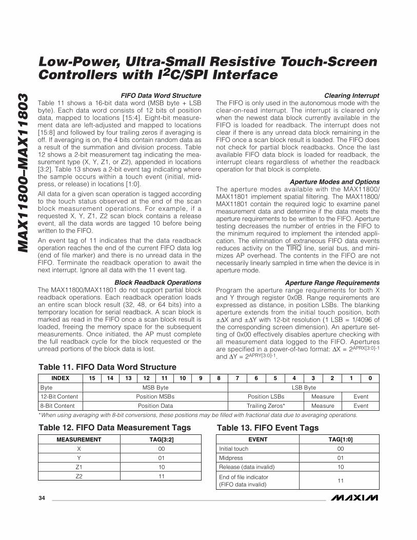
MA
X1
18
00
–MA
X1
18
03
Low-Power, Ultra-Small Resistive Touch-ScreenControllers with I2C/SPI Interface
34 ______________________________________________________________________________________
FIFO Data Word StructureTable 11 shows a 16-bit data word (MSB byte + LSBbyte). Each data word consists of 12 bits of positiondata, mapped to locations [15:4]. Eight-bit measure-ment data are left-adjusted and mapped to locations[15:8] and followed by four trailing zeros if averaging isoff. If averaging is on, the 4 bits contain random data asa result of the summation and division process. Table12 shows a 2-bit measurement tag indicating the mea-surement type (X, Y, Z1, or Z2), appended in locations[3:2]. Table 13 shows a 2-bit event tag indicating wherethe sample occurs within a touch event (initial, mid-press, or release) in locations [1:0].
All data for a given scan operation is tagged accordingto the touch status observed at the end of the scanblock measurement operations. For example, if arequested X, Y, Z1, Z2 scan block contains a releaseevent, all the data words are tagged 10 before beingwritten to the FIFO.
An event tag of 11 indicates that the data readbackoperation reaches the end of the current FIFO data log(end of file marker) and there is no unread data in theFIFO. Terminate the readback operation to await thenext interrupt. Ignore all data with the 11 event tag.
Block Readback OperationsThe MAX11800/MAX11801 do not support partial blockreadback operations. Each readback operation loadsan entire scan block result (32, 48, or 64 bits) into atemporary location for serial readback. A scan block ismarked as read in the FIFO once a scan block result isloaded, freeing the memory space for the subsequentmeasurements. Once initiated, the AP must completethe full readback cycle for the block requested or theunread portions of the block data is lost.
Clearing InterruptThe FIFO is only used in the autonomous mode with theclear-on-read interrupt. The interrupt is cleared onlywhen the newest data block currently available in theFIFO is loaded for readback. The interrupt does notclear if there is any unread data block remaining in theFIFO once a scan block result is loaded. The FIFO doesnot check for partial block readbacks. Once the lastavailable FIFO data block is loaded for readback, theinterrupt clears regardless of whether the readbackoperation for that block is complete.
Aperture Modes and OptionsThe aperture modes available with the MAX11800/MAX11801 implement spatial filtering. The MAX11800/MAX11801 contain the required logic to examine panelmeasurement data and determine if the data meets theaperture requirements to be written to the FIFO. Aperturetesting decreases the number of entries in the FIFO tothe minimum required to implement the intended appli-cation. The elimination of extraneous FIFO data eventsreduces activity on the TIRQ line, serial bus, and mini-mizes AP overhead. The contents in the FIFO are notnecessarily linearly sampled in time when the device is inaperture mode.
Aperture Range RequirementsProgram the aperture range requirements for both Xand Y through register 0x0B. Range requirements areexpressed as distance, in position LSBs. The blankingaperture extends from the initial touch position, both±ΔX and ±ΔY with 12-bit resolution (1 LSB = 1/4096 ofthe corresponding screen dimension). An aperture set-ting of 0x00 effectively disables aperture checking withall measurement data logged to the FIFO. Aperturesare specified in a power-of-two format: ΔX = 2APRX[3:0]-1
and ΔY = 2APRY[3:0]-1.
EVENT TAG[1:0]
Initial touch 00
Midpress 01
Release (data invalid) 10
End of file indicator(FIFO data invalid)
11
Table 13. FIFO Event TagsMEASUREMENT TAG[3:2]
X 00
Y 01
Z1 10
Z2 11
Table 12. FIFO Data Measurement Tags
INDEX 15 14 13 12 11 10 9 8 7 6 5 4 3 2 1 0
Byte MSB Byte LSB Byte
12-Bit Content Position MSBs Position LSBs Measure Event
8-Bit Content Position Data Trailing Zeros* Measure Event
Table 11. FIFO Data Word Structure
*When using averaging with 8-bit conversions, these positions may be filled with fractional data due to averaging operations.
MA
X1
18
00
–MA
X1
18
03
Low-Power, Ultra-Small Resistive Touch-ScreenControllers with I2C/SPI Interface
______________________________________________________________________________________ 35
For example:
0000 = 2-1 LSB = aperture checking disabled
0001 = 2(1-1) LSB = ±1 LSB
0010 = 2(2-1) LSB = ±2 LSB
0011 = 2(3-1) LSB = ±4 LSB
…
1001 = 2(9-1) LSB = ±256 LSB (1/16 of the touch screenin each direction)
1010 = 2(10-1) LSB = ±512 LSB (1/8 of the touch screenin each direction)
1011 = 2(11-1) LSB = ±1024 LSB (1/4 of the touchscreen in each direction)
1100 = 2(12-1) LSB = ±2048 LSB (1/2 of the touchscreen in each direction)
1101 to 1111 = aperture checking disabled
FIFO Aperture CriteriaIn autonomous mode with aperture engaged, new datais written to the FIFO, and an interrupt is issued whenthe following conditions occur (aperture mode is notavailable in direct conversion mode).
New Panel Touch InitiatedThe FIFO updates and issues an interrupt when a newtouch is observed on the panel (data tag = 00). Thisevent occurs regardless of the current aperture settingand the previous touch location so that multiple pressesin the same location can be observed and registered.
Continuous Panel Touch TerminatedThe FIFO updates and issues an interrupt when a con-tinuous panel touch is terminated (data tag = 10). Thisevent occurs regardless of the current aperture settingand the previous continuous touch location(s) so thatmultiple presses in the same location can be observedand registered.
Continuous Panel TouchMeasurement Meets Aperture Criteria
The MAX11800/MAX11801 log the measurement datato the FIFO and issue an interrupt when a measurementduring a continuous panel touch (event tag = 01) meetsthe aperture criteria (i.e., lies on or outside the apertureboundary). This event occurs when the point of contactis dragged across the touch screen. Only the ΔX or ΔYaperture criteria need to be met and a greater than orequal to qualification criterion is applied. If the changein X position or change in Y position exceeds the aper-ture criteria, then an interrupt is generated.
Applications InformationUsing Aperture Mode
Aperture mode is only supported in the MAX11800/MAX11801. The MAX11800/MAX11801 accommodatetouch-panel applications where limited resolution inboth time and space can be traded off for reducedmicroprocessor activity. A simulated keypad is anexample of an application where autonomous conver-sion mode with aperture checking could yield an effi-cient solution.
The AP determines the durations of touch-screenpresses. An issuance of TIRQ interrupts accompaniesall FIFO events. The interrupts clear when all existingdata is read back by the AP, allowing the AP to correct-ly interpret held panel data.
The FIFO updates immediately when a new touch eventis detected. The system assumes that the panel touch iscontinuous after the AP receives the interrupt. TheMAX11800/MAX11801 continue to scan the panel at theuser-programmed sample rate. The FIFO updates whenthe measurement data shows that the panel touch loca-tion moves (i.e., a measurement exceeds either of theselected aperture ranges). The FIFO also updates upondetection of a panel release. The AP determines theduration of the press by observing the time between theleading edge of the touch (tag 00) and the release edgeof the touch (tag 10). All midpress data (tag 01) are inter-preted as part of a dragged touch event.
All valid touch events log two data points into the FIFO:an initial data point at the beginning of the touch (tag00) and a release data point at the termination of thetouch (tag 10). Discard release edge position data asinvalid as the MAX11800/MAX11801 cannot determineat which point in the ADC conversion cycle the panel isreleased during the measurement operation. If therelease occurs while the ADC is actively sampling thepanel, the results are invalid. Only initial and midpressposition data are reliable.
Any touch event too short in duration to log both initialand release data points is recorded in the FIFO as arelease (tag 10) and discarded as a glitch event.
Measuring durations of panel touches becomesimpractical when the AP services the MAX11800/MAX11801 at lower than the operating speed of thedevices and the panel combined. The AP cannot timethe duration between panel touches when both the ini-tial and release data points can be logged before theinitial interrupt is serviced. Do not allow the FIFO tooverflow as touch information can be lost and the FIFOcontent becomes invalid.
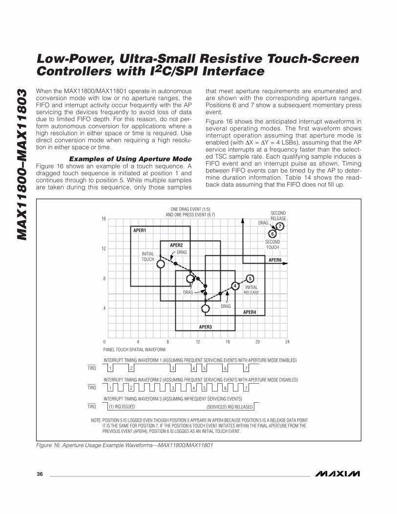
MA
X1
18
00
–MA
X1
18
03
Low-Power, Ultra-Small Resistive Touch-ScreenControllers with I2C/SPI Interface
36 ______________________________________________________________________________________
0 4 8 12 16 20
4
8
12
16
6
7
24
INTERRUPT TIMING WAVEFORM 1 (ASSUMING FREQUENT SERVICING EVENTS WITH APERTURE MODE ENABLED)
PANEL TOUCH SPATIAL WAVEFORM
ONE DRAG EVENT (1:5)AND ONE PRESS EVENT (6:7)
INTERRUPT TIMING WAVEFORM 3 (ASSUMING INFREQUENT SERVICING EVENTS)
NOTE: POSITION 5 IS LOGGED EVEN THOUGH POSITION 5 APPEARS IN APER4 BECAUSE POSITION 5 IS A RELEASE DATA POINT. IT IS THE SAME FOR POSITION 7. IF THE POSITION 6 TOUCH EVENT INITIATES WITHIN THE FINAL APERTURE FROM THE PREVIOUS EVENT (APER4), POSITION 6 IS LOGGED AS AN INITIAL TOUCH EVENT.
(1) IRQ ISSUED (SERVICED) IRQ RELEASED
INTERRUPT TIMING WAVEFORM 2 (ASSUMING FREQUENT SERVICING EVENTS WITH APERTURE MODE DISABLED)
1 2 3 4 5 76
1 2 3 4 5 76
1
2
4
5
3
INITIALTOUCH
INITIALRELEASE
SECONDRELEASE
SECONDTOUCH
DRAG
DRAG
DRAG
DRAG
APER6
APER4
APER3
APER2
APER1
TIRQ
TIRQ
TIRQ
Figure 16. Aperture Usage Example Waveforms—MAX11800/MAX11801
When the MAX11800/MAX11801 operate in autonomousconversion mode with low or no aperture ranges, theFIFO and interrupt activity occur frequently with the APservicing the devices frequently to avoid loss of datadue to limited FIFO depth. For this reason, do not per-form autonomous conversion for applications where ahigh resolution in either space or time is required. Usedirect conversion mode when requiring a high resolu-tion in either space or time.
Examples of Using Aperture ModeFigure 16 shows an example of a touch sequence. Adragged touch sequence is initiated at position 1 andcontinues through to position 5. While multiple samplesare taken during this sequence, only those samples
that meet aperture requirements are enumerated andare shown with the corresponding aperture ranges.Positions 6 and 7 show a subsequent momentary pressevent.
Figure 16 shows the anticipated interrupt waveforms inseveral operating modes. The first waveform showsinterrupt operation assuming that aperture mode isenabled (with ΔX = ΔY = 4 LSBs), assuming that the APservice interrupts at a frequency faster than the select-ed TSC sample rate. Each qualifying sample induces aFIFO event and an interrupt pulse as shown. Timingbetween FIFO events can be timed by the AP to deter-mine duration information. Table 14 shows the read-back data assuming that the FIFO does not fill up.
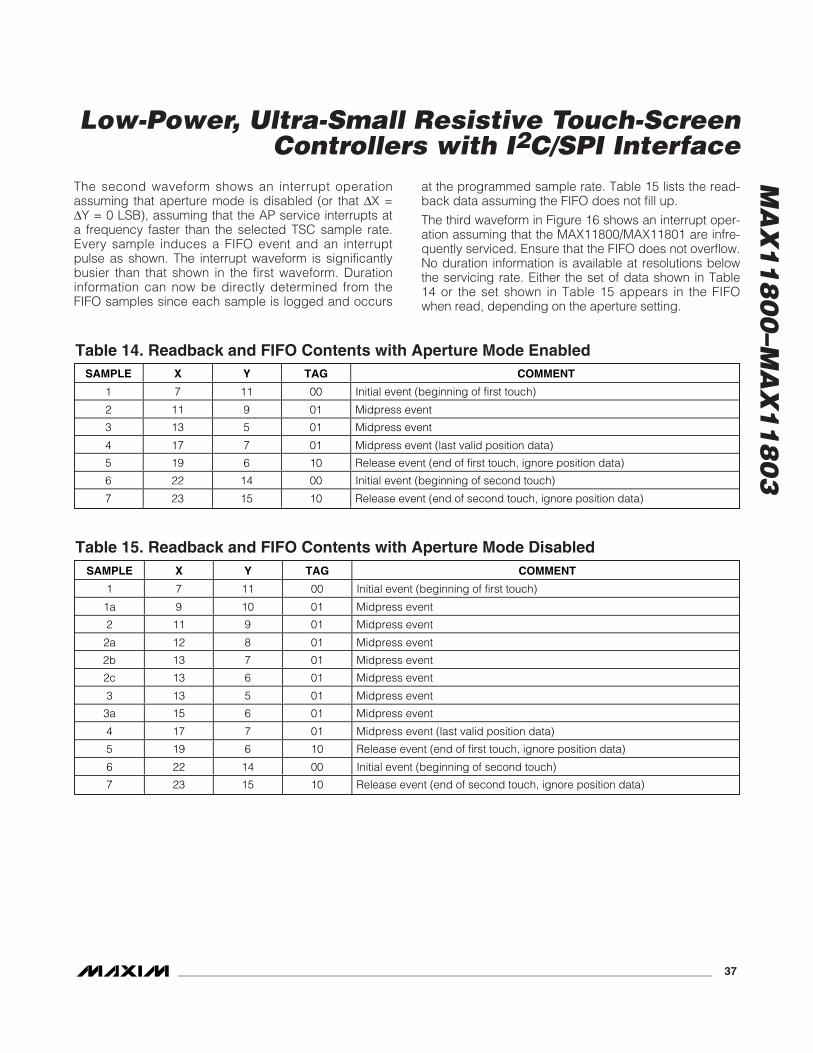
MA
X1
18
00
–MA
X1
18
03
Low-Power, Ultra-Small Resistive Touch-ScreenControllers with I2C/SPI Interface
______________________________________________________________________________________ 37
SAMPLE X Y TAG COMMENT
1 7 11 00 Initial event (beginning of first touch)
1a 9 10 01 Midpress event
2 11 9 01 Midpress event
2a 12 8 01 Midpress event
2b 13 7 01 Midpress event
2c 13 6 01 Midpress event
3 13 5 01 Midpress event
3a 15 6 01 Midpress event
4 17 7 01 Midpress event (last valid position data)
5 19 6 10 Release event (end of first touch, ignore position data)
6 22 14 00 Initial event (beginning of second touch)
7 23 15 10 Release event (end of second touch, ignore position data)
Table 15. Readback and FIFO Contents with Aperture Mode Disabled
SAMPLE X Y TAG COMMENT
1 7 11 00 Initial event (beginning of first touch)
2 11 9 01 Midpress event
3 13 5 01 Midpress event
4 17 7 01 Midpress event (last valid position data)
5 19 6 10 Release event (end of first touch, ignore position data)
6 22 14 00 Initial event (beginning of second touch)
7 23 15 10 Release event (end of second touch, ignore position data)
Table 14. Readback and FIFO Contents with Aperture Mode Enabled
The second waveform shows an interrupt operationassuming that aperture mode is disabled (or that ΔX =ΔY = 0 LSB), assuming that the AP service interrupts ata frequency faster than the selected TSC sample rate.Every sample induces a FIFO event and an interruptpulse as shown. The interrupt waveform is significantlybusier than that shown in the first waveform. Durationinformation can now be directly determined from theFIFO samples since each sample is logged and occurs
at the programmed sample rate. Table 15 lists the read-back data assuming the FIFO does not fill up.
The third waveform in Figure 16 shows an interrupt oper-ation assuming that the MAX11800/MAX11801 are infre-quently serviced. Ensure that the FIFO does not overflow.No duration information is available at resolutions belowthe servicing rate. Either the set of data shown in Table14 or the set shown in Table 15 appears in the FIFOwhen read, depending on the aperture setting.
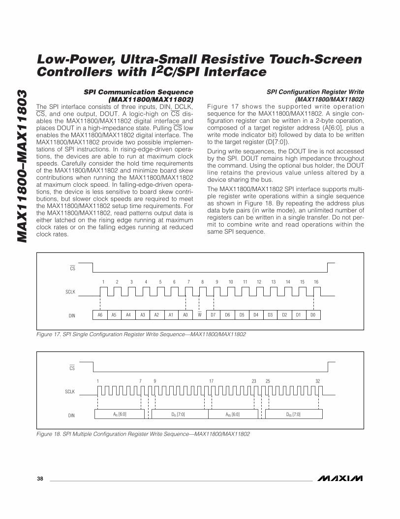
MA
X1
18
00
–MA
X1
18
03
Low-Power, Ultra-Small Resistive Touch-ScreenControllers with I2C/SPI Interface
38 ______________________________________________________________________________________
CS
SCLK
DIN An [6:0]
1 9 17 25 327 23
Dn [7:0] Am [6:0] Dm [7:0]
Figure 18. SPI Multiple Configuration Register Write Sequence—MAX11800/MAX11802
SPI Communication Sequence(MAX11800/MAX11802)
The SPI interface consists of three inputs, DIN, DCLK,CS, and one output, DOUT. A logic-high on CS dis-ables the MAX11800/MAX11802 digital interface andplaces DOUT in a high-impedance state. Pulling CS lowenables the MAX11800/MAX11802 digital interface. TheMAX11800/MAX11802 provide two possible implemen-tations of SPI instructions. In rising-edge-driven opera-tions, the devices are able to run at maximum clockspeeds. Carefully consider the hold time requirementsof the MAX11800/MAX11802 and minimize board skewcontributions when running the MAX11800/MAX11802at maximum clock speed. In falling-edge-driven opera-tions, the device is less sensitive to board skew contri-butions, but slower clock speeds are required to meetthe MAX11800/MAX11802 setup time requirements. Forthe MAX11800/MAX11802, read patterns output data iseither latched on the rising edge running at maximumclock rates or on the falling edges running at reducedclock rates.
SPI Configuration Register Write(MAX11800/MAX11802)
Figure 17 shows the supported write operationsequence for the MAX11800/MAX11802. A single con-figuration register can be written in a 2-byte operation,composed of a target register address (A[6:0], plus awrite mode indicator bit) followed by data to be writtento the target register (D[7:0]).
During write sequences, the DOUT line is not accessedby the SPI. DOUT remains high impedance throughoutthe command. Using the optional bus holder, the DOUTline retains the previous value unless altered by adevice sharing the bus.
The MAX11800/MAX11802 SPI interface supports multi-ple register write operations within a single sequenceas shown in Figure 18. By repeating the address plusdata byte pairs (in write mode), an unlimited number ofregisters can be written in a single transfer. Do not per-mit to combine write and read operations within thesame SPI sequence.
CS
SCLK
DIN
161 2 3 4 5 6 7 8 9 10 11 12 13 14 15
A6 A5 A4 A3 A2 A1 WA0 D6 D5 D4 D3 D2 D1 D0D7
Figure 17. SPI Single Configuration Register Write Sequence—MAX11800/MAX11802
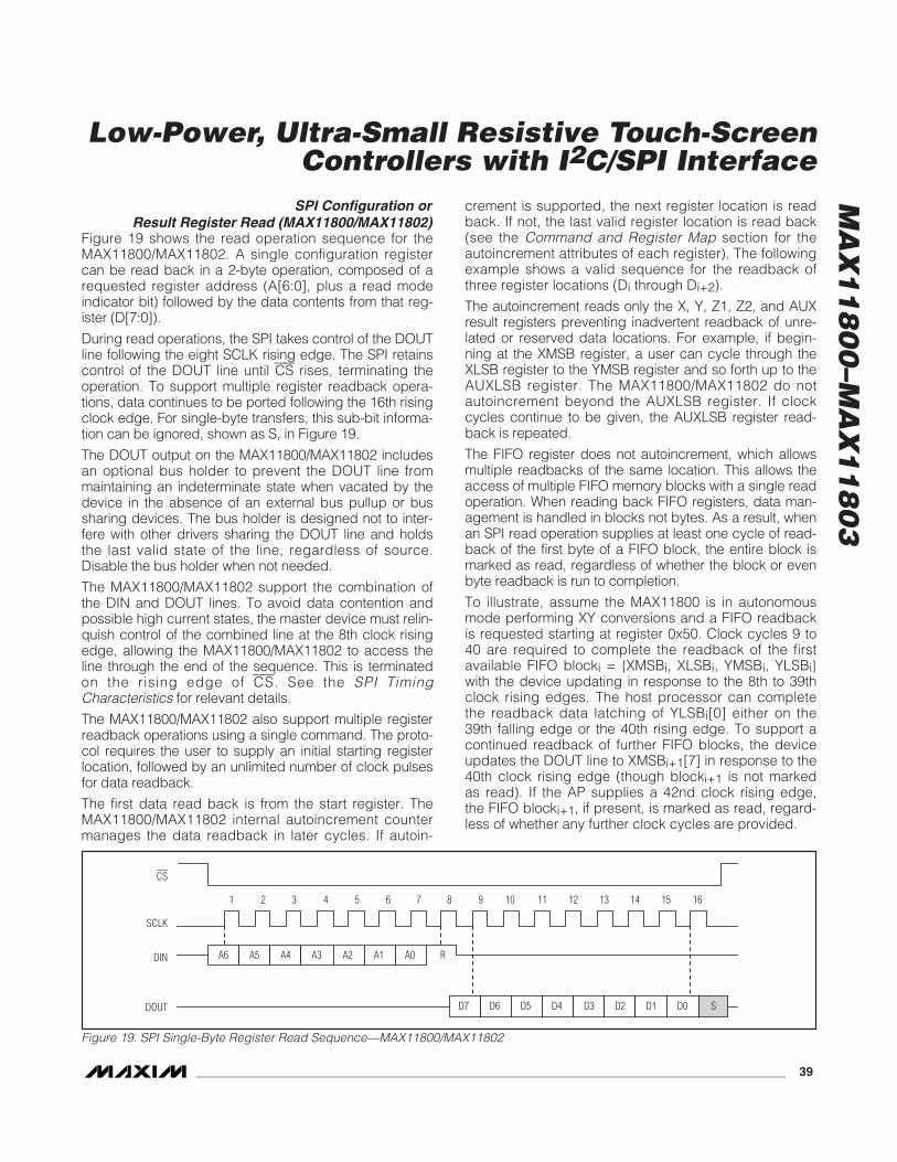
MA
X1
18
00
–MA
X1
18
03
Low-Power, Ultra-Small Resistive Touch-ScreenControllers with I2C/SPI Interface
______________________________________________________________________________________ 39
SPI Configuration or Result Register Read (MAX11800/MAX11802)
Figure 19 shows the read operation sequence for theMAX11800/MAX11802. A single configuration registercan be read back in a 2-byte operation, composed of arequested register address (A[6:0], plus a read modeindicator bit) followed by the data contents from that reg-ister (D[7:0]).
During read operations, the SPI takes control of the DOUTline following the eight SCLK rising edge. The SPI retainscontrol of the DOUT line until CS rises, terminating theoperation. To support multiple register readback opera-tions, data continues to be ported following the 16th risingclock edge. For single-byte transfers, this sub-bit informa-tion can be ignored, shown as S, in Figure 19.
The DOUT output on the MAX11800/MAX11802 includesan optional bus holder to prevent the DOUT line frommaintaining an indeterminate state when vacated by thedevice in the absence of an external bus pullup or bussharing devices. The bus holder is designed not to inter-fere with other drivers sharing the DOUT line and holdsthe last valid state of the line, regardless of source.Disable the bus holder when not needed.
The MAX11800/MAX11802 support the combination ofthe DIN and DOUT lines. To avoid data contention andpossible high current states, the master device must relin-quish control of the combined line at the 8th clock risingedge, allowing the MAX11800/MAX11802 to access theline through the end of the sequence. This is terminatedon the rising edge of CS. See the SPI TimingCharacteristics for relevant details.
The MAX11800/MAX11802 also support multiple registerreadback operations using a single command. The proto-col requires the user to supply an initial starting registerlocation, followed by an unlimited number of clock pulsesfor data readback.
The first data read back is from the start register. TheMAX11800/MAX11802 internal autoincrement countermanages the data readback in later cycles. If autoin-
crement is supported, the next register location is readback. If not, the last valid register location is read back(see the Command and Register Map section for theautoincrement attributes of each register). The followingexample shows a valid sequence for the readback ofthree register locations (Di through Di+2).
The autoincrement reads only the X, Y, Z1, Z2, and AUXresult registers preventing inadvertent readback of unre-lated or reserved data locations. For example, if begin-ning at the XMSB register, a user can cycle through theXLSB register to the YMSB register and so forth up to theAUXLSB register. The MAX11800/MAX11802 do notautoincrement beyond the AUXLSB register. If clockcycles continue to be given, the AUXLSB register read-back is repeated.
The FIFO register does not autoincrement, which allowsmultiple readbacks of the same location. This allows theaccess of multiple FIFO memory blocks with a single readoperation. When reading back FIFO registers, data man-agement is handled in blocks not bytes. As a result, whenan SPI read operation supplies at least one cycle of read-back of the first byte of a FIFO block, the entire block ismarked as read, regardless of whether the block or evenbyte readback is run to completion.
To illustrate, assume the MAX11800 is in autonomousmode performing XY conversions and a FIFO readbackis requested starting at register 0x50. Clock cycles 9 to40 are required to complete the readback of the firstavailable FIFO blocki = {XMSBi, XLSBi, YMSBi, YLSBi}with the device updating in response to the 8th to 39thclock rising edges. The host processor can completethe readback data latching of YLSBi[0] either on the39th falling edge or the 40th rising edge. To support acontinued readback of further FIFO blocks, the deviceupdates the DOUT line to XMSBi+1[7] in response to the40th clock rising edge (though blocki+1 is not markedas read). If the AP supplies a 42nd clock rising edge,the FIFO blocki+1, if present, is marked as read, regard-less of whether any further clock cycles are provided.
CS
SCLK
DIN
161 2 3 4 5 6 7 8 9 10 11 12 13 14 15
A6 A5 A4 A3 A2 A1 RA0
D6 D5 D4 D3 D2 D1 D0D7DOUT S
Figure 19. SPI Single-Byte Register Read Sequence—MAX11800/MAX11802
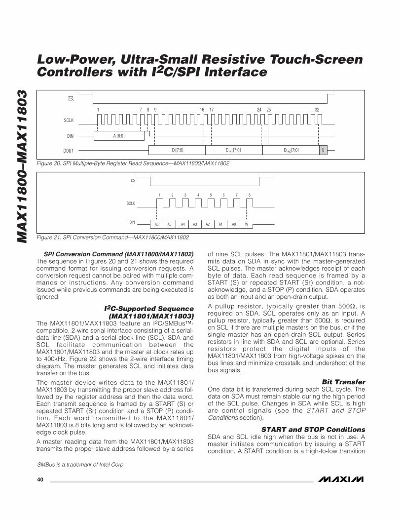
MA
X1
18
00
–MA
X1
18
03
Low-Power, Ultra-Small Resistive Touch-ScreenControllers with I2C/SPI Interface
40 ______________________________________________________________________________________
SPI Conversion Command (MAX11800/MAX11802)The sequence in Figures 20 and 21 shows the requiredcommand format for issuing conversion requests. Aconversion request cannot be paired with multiple com-mands or instructions. Any conversion commandissued while previous commands are being executed isignored.
I2C-Supported Sequence(MAX11801/MAX11803)
The MAX11801/MAX11803 feature an I2C/SMBus™-compatible, 2-wire serial interface consisting of a serial-data line (SDA) and a serial-clock line (SCL). SDA andSCL facil i tate communication between theMAX11801/MAX11803 and the master at clock rates upto 400kHz. Figure 22 shows the 2-wire interface timingdiagram. The master generates SCL and initiates datatransfer on the bus.
The master device writes data to the MAX11801/MAX11803 by transmitting the proper slave address fol-lowed by the register address and then the data word.Each transmit sequence is framed by a START (S) orrepeated START (Sr) condition and a STOP (P) condi-t ion. Each word transmitted to the MAX11801/MAX11803 is 8 bits long and is followed by an acknowl-edge clock pulse.
A master reading data from the MAX11801/MAX11803transmits the proper slave address followed by a series
of nine SCL pulses. The MAX11801/MAX11803 trans-mits data on SDA in sync with the master-generatedSCL pulses. The master acknowledges receipt of eachbyte of data. Each read sequence is framed by aSTART (S) or repeated START (Sr) condition, a not-acknowledge, and a STOP (P) condition. SDA operatesas both an input and an open-drain output.
A pullup resistor, typically greater than 500Ω, isrequired on SDA. SCL operates only as an input. Apullup resistor, typically greater than 500Ω, is requiredon SCL if there are multiple masters on the bus, or if thesingle master has an open-drain SCL output. Seriesresistors in line with SDA and SCL are optional. Seriesresistors protect the digital inputs of theMAX11801/MAX11803 from high-voltage spikes on thebus lines and minimize crosstalk and undershoot of thebus signals.
Bit TransferOne data bit is transferred during each SCL cycle. Thedata on SDA must remain stable during the high periodof the SCL pulse. Changes in SDA while SCL is highare control signals (see the START and STOPConditions section).
START and STOP ConditionsSDA and SCL idle high when the bus is not in use. Amaster initiates communication by issuing a STARTcondition. A START condition is a high-to-low transition
CS
SCLK
DIN
1 2 3 4 5 6 7 8
A6 A5 A4 A3 A2 A1 WA0
Figure 21. SPI Conversion Command—MAX11800/MAX11802
CS
SCLK
DIN Ai[6:0]
1 9 17 25 327 2416
DOUT
8
SDi[7:0] Di+1[7:0] Di+2[7:0]
Figure 20. SPI Multiple-Byte Register Read Sequence—MAX11800/MAX11802
SMBus is a trademark of Intel Corp.
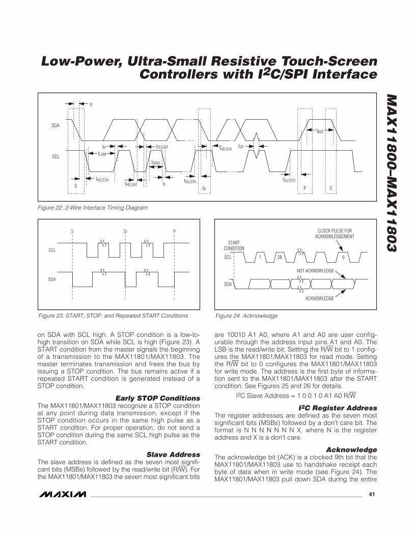
MA
X1
18
00
–MA
X1
18
03
Low-Power, Ultra-Small Resistive Touch-ScreenControllers with I2C/SPI Interface
______________________________________________________________________________________ 41
on SDA with SCL high. A STOP condition is a low-to-high transition on SDA while SCL is high (Figure 23). ASTART condition from the master signals the beginningof a transmission to the MAX11801/MAX11803. Themaster terminates transmission and frees the bus byissuing a STOP condition. The bus remains active if arepeated START condition is generated instead of aSTOP condition.
Early STOP ConditionsThe MAX11801/MAX11803 recognize a STOP conditionat any point during data transmission, except if theSTOP condition occurs in the same high pulse as aSTART condition. For proper operation, do not send aSTOP condition during the same SCL high pulse as theSTART condition.
Slave AddressThe slave address is defined as the seven most signifi-cant bits (MSBs) followed by the read/write bit (R/W). Forthe MAX11801/MAX11803 the seven most significant bits
are 10010 A1 A0, where A1 and A0 are user config-urable through the address input pins A1 and A0. TheLSB is the read/write bit. Setting the R/W bit to 1 config-ures the MAX11801/MAX11803 for read mode. Settingthe R/W bit to 0 configures the MAX11801/MAX11803for write mode. The address is the first byte of informa-tion sent to the MAX11801/MAX11803 after the STARTcondition. See Figures 25 and 26 for details.
I2C Slave Address = 1 0 0 1 0 A1 A0 R/W
I2C Register AddressThe register addresses are defined as the seven mostsignificant bits (MSBs) followed by a don’t care bit. Theformat is N N N N N N N X, where N is the registeraddress and X is a don’t care.
AcknowledgeThe acknowledge bit (ACK) is a clocked 9th bit that theMAX11801/MAX11803 use to handshake receipt eachbyte of data when in write mode (see Figure 24). TheMAX11801/MAX11803 pull down SDA during the entire
1 28 9
STARTCONDITION
SCL
SDA
ACKNOWLEDGE
NOT ACKNOWLEDGE
CLOCK PULSE FORACKNOWLEDGEMENT
Figure 24. Acknowledge
SCL
SDA
S Sr P
Figure 23. START, STOP, and Repeated START Conditions
Figure 22. 2-Wire Interface Timing Diagram
SDA
SCL
S
tF
tHD;STA
tLOW
tR
tHD;DAT
tSU;DAT
tHIGH
tFtSU;STA
tHD;STA
Sr
tSP
tBUF
tSU;STO
P S
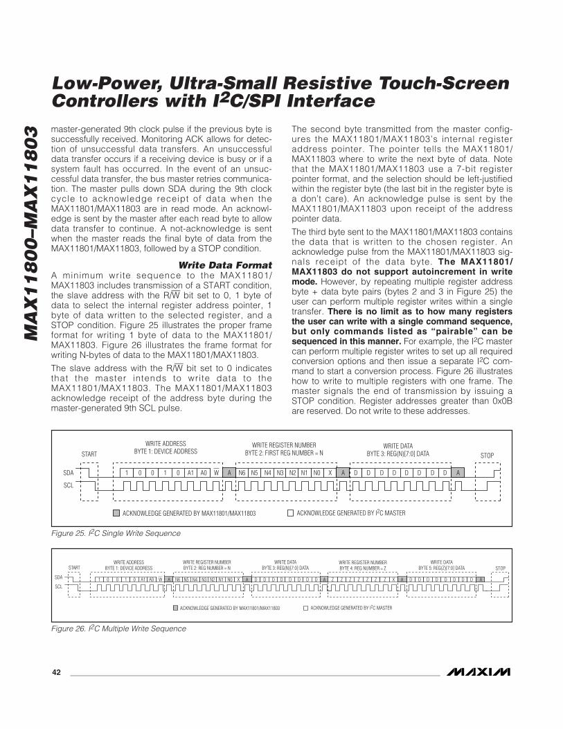
MA
X1
18
00
–MA
X1
18
03 master-generated 9th clock pulse if the previous byte is
successfully received. Monitoring ACK allows for detec-tion of unsuccessful data transfers. An unsuccessfuldata transfer occurs if a receiving device is busy or if asystem fault has occurred. In the event of an unsuc-cessful data transfer, the bus master retries communica-tion. The master pulls down SDA during the 9th clockcycle to acknowledge receipt of data when theMAX11801/MAX11803 are in read mode. An acknowl-edge is sent by the master after each read byte to allowdata transfer to continue. A not-acknowledge is sentwhen the master reads the final byte of data from theMAX11801/MAX11803, followed by a STOP condition.
Write Data FormatA minimum write sequence to the MAX11801/MAX11803 includes transmission of a START condition,the slave address with the R/W bit set to 0, 1 byte ofdata to select the internal register address pointer, 1byte of data written to the selected register, and aSTOP condition. Figure 25 illustrates the proper frameformat for writing 1 byte of data to the MAX11801/MAX11803. Figure 26 illustrates the frame format forwriting N-bytes of data to the MAX11801/MAX11803.
The slave address with the R/W bit set to 0 indicatesthat the master intends to write data to theMAX11801/MAX11803. The MAX11801/MAX11803acknowledge receipt of the address byte during themaster-generated 9th SCL pulse.
The second byte transmitted from the master config-ures the MAX11801/MAX11803’s internal registeraddress pointer. The pointer tells the MAX11801/MAX11803 where to write the next byte of data. Notethat the MAX11801/MAX11803 use a 7-bit registerpointer format, and the selection should be left-justifiedwithin the register byte (the last bit in the register byte isa don’t care). An acknowledge pulse is sent by theMAX11801/MAX11803 upon receipt of the addresspointer data.
The third byte sent to the MAX11801/MAX11803 containsthe data that is written to the chosen register. Anacknowledge pulse from the MAX11801/MAX11803 sig-nals receipt of the data byte. The MAX11801/MAX11803 do not support autoincrement in writemode. However, by repeating multiple register addressbyte + data byte pairs (bytes 2 and 3 in Figure 25) theuser can perform multiple register writes within a singletransfer. There is no limit as to how many registersthe user can write with a single command sequence,but only commands listed as “pairable” can besequenced in this manner. For example, the I2C mastercan perform multiple register writes to set up all requiredconversion options and then issue a separate I2C com-mand to start a conversion process. Figure 26 illustrateshow to write to multiple registers with one frame. Themaster signals the end of transmission by issuing aSTOP condition. Register addresses greater than 0x0Bare reserved. Do not write to these addresses.
Low-Power, Ultra-Small Resistive Touch-ScreenControllers with I2C/SPI Interface
42 ______________________________________________________________________________________
STARTWRITE ADDRESS
BYTE 1: DEVICE ADDRESSWRITE REGISTER NUMBERBYTE 2: REG NUMBER = N
WRITE DATABYTE 3: REG(N)[7:0] DATA STOP
W N3 N2 N1 N0 X D D D D D D D DN41 0 0 1 0 A1 A0 N5N6 Z Z Z Z X D D D D D D D DZZZ
WRITE DATABYTE 5: REG(Z)[7:0] DATA
WRITE REGISTER NUMBERBYTE 4: REG NUMBER = Z
SDA
SCLA A A A A
ACKNOWLEDGE GENERATED BY I2C MASTERACKNOWLEDGE GENERATED BY MAX11801/MAX11803
Figure 26. I2C Multiple Write Sequence
SCL
W N3 N2 N1 N0 X D D D D D D D D
START
SDA
WRITE ADDRESSBYTE 1: DEVICE ADDRESS
WRITE REGISTER NUMBERBYTE 2: FIRST REG NUMBER = N
WRITE DATABYTE 3: REG(N)[7:0] DATA STOP
N41 0 0 1 0 A1 A0 N5N6A A A
ACKNOWLEDGE GENERATED BY I2C MASTERACKNOWLEDGE GENERATED BY MAX11801/MAX11803
Figure 25. I2C Single Write Sequence
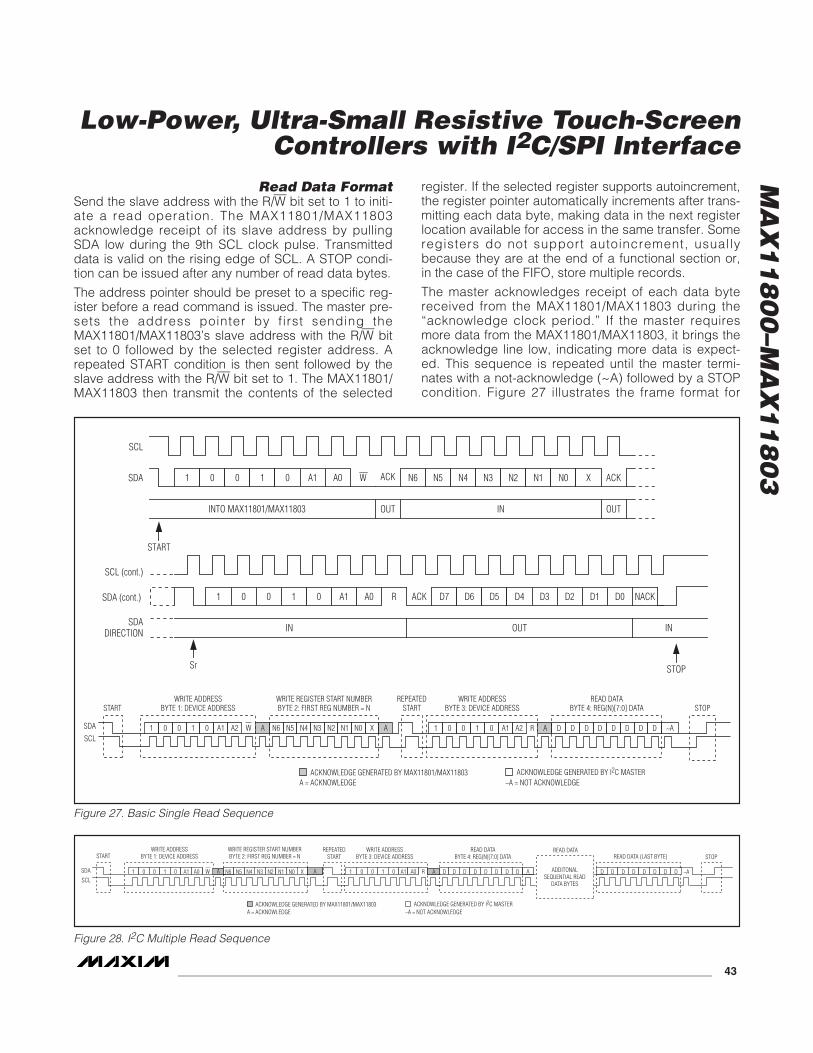
Read Data FormatSend the slave address with the R/W bit set to 1 to initi-ate a read operation. The MAX11801/MAX11803acknowledge receipt of its slave address by pullingSDA low during the 9th SCL clock pulse. Transmitteddata is valid on the rising edge of SCL. A STOP condi-tion can be issued after any number of read data bytes.
The address pointer should be preset to a specific reg-ister before a read command is issued. The master pre-sets the address pointer by first sending theMAX11801/MAX11803’s slave address with the R/W bitset to 0 followed by the selected register address. Arepeated START condition is then sent followed by theslave address with the R/W bit set to 1. The MAX11801/MAX11803 then transmit the contents of the selected
register. If the selected register supports autoincrement,the register pointer automatically increments after trans-mitting each data byte, making data in the next registerlocation available for access in the same transfer. Someregisters do not support autoincrement, usuallybecause they are at the end of a functional section or,in the case of the FIFO, store multiple records.
The master acknowledges receipt of each data bytereceived from the MAX11801/MAX11803 during the“acknowledge clock period.” If the master requiresmore data from the MAX11801/MAX11803, it brings theacknowledge line low, indicating more data is expect-ed. This sequence is repeated until the master termi-nates with a not-acknowledge (~A) followed by a STOPcondition. Figure 27 illustrates the frame format for
MA
X1
18
00
–MA
X1
18
03
Low-Power, Ultra-Small Resistive Touch-ScreenControllers with I2C/SPI Interface
______________________________________________________________________________________ 43
STARTWRITE ADDRESS
BYTE 1: DEVICE ADDRESSWRITE REGISTER START NUMBERBYTE 2: FIRST REG NUMBER = N STOP
W N3 N2 N1 N0 X D D D D D D D D
READ DATABYTE 4: REG(N)[7:0] DATA
REPEATEDSTART
ADDITONALSEQUENTIAL READ
DATA BYTES
READ DATA
D D D D D D D ~AD
READ DATA (LAST BYTE)
R
WRITE ADDRESSBYTE 3: DEVICE ADDRESS
ACKNOWLEDGE GENERATED BY I2C MASTERACKNOWLEDGE GENERATED BY MAX11801/MAX11803
N4N5N61 0 0 1 0 A1 A0 1 0 0 1 0 A1 A0SDA
SCLA A A A
A = ACKNOWLEDGE ~A = NOT ACKNOWLEDGE
Figure 28. I2C Multiple Read Sequence
SDA
SDADIRECTION
SCL
1 0 0 1 0 A1 A0 W N6 N5 N4 N3 N2 N1 N0 XACK ACK
OUTINOUTINTO MAX11801/MAX11803
SDA (cont.)
SCL (cont.)
0 A1 D7 D6 D5 D4 D3 D2 D1 D0ACK
OUT
A0
IN IN
START
1 0 0 1 R
Sr STOP
NACK
STARTWRITE ADDRESS
BYTE 1: DEVICE ADDRESSWRITE REGISTER START NUMBERBYTE 2: FIRST REG NUMBER = N STOP
READ DATA BYTE 4: REG(N)[7:0] DATA
REPEATED START
WRITE ADDRESS BYTE 3: DEVICE ADDRESS
ACKNOWLEDGE GENERATED BY I2C MASTERACKNOWLEDGE GENERATED BY MAX11801/MAX11803A = ACKNOWLEDGE ~A = NOT ACKNOWLEDGE
1SDA
SCL0 0 1 0 A1 N6 N5 N4 N3 N2 N1 N0 1 0 0 1 0 A1 A D D D D D D D D ~ARA2X AA2 AW
Figure 27. Basic Single Read Sequence
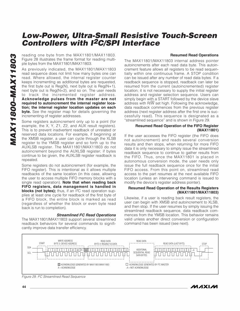
MA
X1
18
00
–MA
X1
18
03 reading one byte from the MAX11801/MAX11803.
Figure 28 illustrates the frame format for reading multi-ple bytes from the MAX11801/MAX11803.
As previously indicated, the MAX11801/MAX11803read sequence does not limit how many bytes one canread. Where allowed, the internal register counterkeeps incrementing as additional bytes are requested,the first byte out is Reg(N), next byte out is Reg(N+1),next byte out is Reg(N+2), and so on. The user needsto track the incremented register address.Acknowledge pulses from the master are notrequired to autoincrement the internal register loca-tion; the internal register location updates on eachbyte. See the register map for details governing theincrementing of register addresses.
Some registers autoincrement only up to a point (forexample, the X, Y, Z1, Z2, and AUX result registers).This is to prevent inadvertent readback of unrelated orreserved data locations. For example, if beginning atthe XMSB register, a user can cycle through the XLSBregister to the YMSB register and so forth up to theAUXLSB register. The MAX11801/MAX11803 do notautoincrement beyond the AUXLSB register; if bytescontinue to be given, the AUXLSB register readback isrepeated.
Some registers do not autoincrement (for example, theFIFO register). This is intentional as it allows multiplereadbacks of the same location (in this case, allowingthe user to access multiple FIFO memory blocks with asingle read operation). Note that when reading backFIFO registers, data management is handled inblocks (not bytes); thus, if an I2C read operation sup-plies at least one cycle for readback of the first byte ofa FIFO block, the entire block is marked as read(regardless of whether the block or even byte readback is run to completion).
Streamlined I2C Read OperationsThe MAX11801/MAX11803 support several streamlinedreadback behaviors for several commands to signifi-cantly improve data transfer efficiency.
Resumed Read Operations
The MAX11801/MAX11803 internal address pointerautoincrements after each read data byte. This autoin-crement feature allows all registers to be read sequen-tially within one continuous frame. A STOP conditioncan be issued after any number of read data bytes. If areadback sequence is stopped, readback can later beresumed from the current (autoincremented) registerlocation; it is not necessary to supply the initial registeraddress and register selection sequence. Users cansimply begin with a START followed by the device slaveaddress with R/W set high. Following the acknowledge,data readback commences from the previous registeraddress (next register address after the first one is suc-cessfully read). This sequence is designated as a“streamlined sequence” and is shown in Figure 29.
Resumed Read Operation of the FIFO Register(MAX11801)
If the user accesses the FIFO register (the FIFO doesnot autoincrement) and reads several conversionresults and then stops, when returning for more FIFOdata it is only necessary to simply issue the streamlinedreadback sequence to continue to gather results fromthe FIFO. Thus, once the MAX11801 is placed inautonomous conversion mode, the user needs onlyissue the full readback sequence once for the initialFIFO access. From this point on, streamlined readaccess to the part resumes at the next available FIFOlocation (unless an intervening command is issued tomodify the device’s register address pointer).
Resumed Read Operation of the Results Registers(MAX11801/MAX11803)
Likewise, if a user is reading back result registers, theuser can begin with XMSB and autoincrement to XLSB,and then stop. If the user resumes by simply issuing thestreamlined readback sequence, data readback com-mences from the YMSB location. This behavior remainsvalid unless another direct conversion or configurationcommand has been issued (see next).
Low-Power, Ultra-Small Resistive Touch-ScreenControllers with I2C/SPI Interface
44 ______________________________________________________________________________________
STARTWRITE ADDRESS
BYTE 3: DEVICE ADDRESS
D D D D D D D D
READ DATABYTE 4: REG(N)[7:0] DATA
ADDITONALSEQUENTIAL READ
DATA BYTES
READ DATASTOP
D D D D D D D ~AD
READ DATA (LAST BYTE)
R
ACKNOWLEDGE GENERATED BY I2C MASTERACKNOWLEDGE GENERATED BY MAX11801/MAX11803
1 0 0 1 0 A1 A0SDA
SCLA A
A = ACKNOWLEDGE ~A = NOT ACKNOWLEDGE
Figure 29. I2C Streamlined Read Sequence
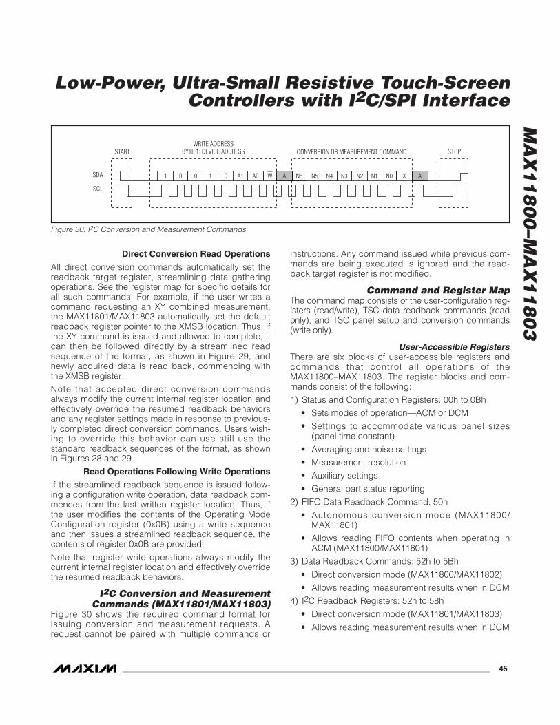
Direct Conversion Read Operations
All direct conversion commands automatically set thereadback target register, streamlining data gatheringoperations. See the register map for specific details forall such commands. For example, if the user writes acommand requesting an XY combined measurement,the MAX11801/MAX11803 automatically set the defaultreadback register pointer to the XMSB location. Thus, ifthe XY command is issued and allowed to complete, itcan then be followed directly by a streamlined readsequence of the format, as shown in Figure 29, andnewly acquired data is read back, commencing withthe XMSB register.
Note that accepted direct conversion commandsalways modify the current internal register location andeffectively override the resumed readback behaviorsand any register settings made in response to previous-ly completed direct conversion commands. Users wish-ing to override this behavior can use still use thestandard readback sequences of the format, as shownin Figures 28 and 29.
Read Operations Following Write Operations
If the streamlined readback sequence is issued follow-ing a configuration write operation, data readback com-mences from the last written register location. Thus, ifthe user modifies the contents of the Operating ModeConfiguration register (0x0B) using a write sequenceand then issues a streamlined readback sequence, thecontents of register 0x0B are provided.
Note that register write operations always modify thecurrent internal register location and effectively overridethe resumed readback behaviors.
I2C Conversion and MeasurementCommands (MAX11801/MAX11803)
Figure 30 shows the required command format forissuing conversion and measurement requests. Arequest cannot be paired with multiple commands or
instructions. Any command issued while previous com-mands are being executed is ignored and the read-back target register is not modified.
Command and Register MapThe command map consists of the user-configuration reg-isters (read/write), TSC data readback commands (readonly), and TSC panel setup and conversion commands(write only).
User-Accessible RegistersThere are six blocks of user-accessible registers andcommands that control al l operations of theMAX11800–MAX11803. The register blocks and com-mands consist of the following:
1) Status and Configuration Registers: 00h to 0Bh
• Sets modes of operation––ACM or DCM
• Settings to accommodate various panel sizes(panel time constant)
• Averaging and noise settings
• Measurement resolution
• Auxiliary settings
• General part status reporting
2) FIFO Data Readback Command: 50h
• Autonomous conversion mode (MAX11800/MAX11801)
• Allows reading FIFO contents when operating inACM (MAX11800/MAX11801)
3) Data Readback Commands: 52h to 5Bh
• Direct conversion mode (MAX11800/MAX11802)
• Allows reading measurement results when in DCM
4) I2C Readback Registers: 52h to 58h
• Direct conversion mode (MAX11801/MAX11803)
• Allows reading measurement results when in DCM
MA
X1
18
00
–MA
X1
18
03
Low-Power, Ultra-Small Resistive Touch-ScreenControllers with I2C/SPI Interface
______________________________________________________________________________________ 45
STARTWRITE ADDRESS
BYTE 1: DEVICE ADDRESS STOP
W N3 N2 N1 N0 X
CONVERSION OR MEASUREMENT COMMAND
N41 0 0 1 0 A1 A0 N5N6SDA
SCL
A A
Figure 30. I2C Conversion and Measurement Commands
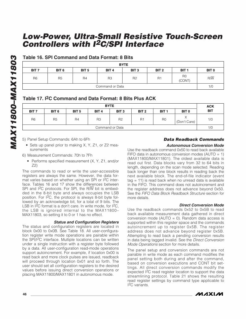
MA
X1
18
00
–MA
X1
18
03
Low-Power, Ultra-Small Resistive Touch-ScreenControllers with I2C/SPI Interface
46 ______________________________________________________________________________________
BYTE
BIT 7 BIT 6 BIT 5 BIT 4 BIT 3 BIT 2 BIT 1 BIT 0ACKBIT
R6 R5 R4 R3 R2 R1 R0 X
(Don’t Care) 1/0
Command or Data 1/0
Table 17. I2C Command and Data Format: 8 Bits Plus ACK
5) Panel Setup Commands: 6Ah to 6Fh
• Sets up panel prior to making X, Y, Z1, or Z2 mea-surements
6) Measurement Commands: 70h to 7Fh
• Performs specified measurement (X, Y, Z1, and/orZ2)
The commands to read or write the user-accessibleregisters are always the same. However, the data for-mat varies based on whether using an SPI or I2C inter-face. Tables 16 and 17 show the differences betweenSPI and I2C protocols. For SPI, the R/W bit is embed-ded in the 8-bit byte and always occupies the LSBposition. For I2C, the protocol is always 8-bit byte fol-lowed by an acknowledge bit, for a total of 9 bits. TheLSB in I2C format is a don’t care. In write mode, for I2C,the LSB is ignored internal to the MAX11800–MAX11803, so setting it to 0 or 1 has no effect.
Status and Configuration Registers The status and configuration registers are located inblock 0x00 to 0x0B. See Table 18. All user-configura-tion register write mode operations are pairable withinthe SPI/I2C interface. Multiple locations can be writtenunder a single instruction with a register byte followedby a data. All user-configuration read-mode operationssupport autoincrement. For example, if location 0x00 isread back and more clock pulses are issued, readbackwill proceed through location 0x01 and so forth. Theuser should set all configuration registers to the desiredvalues before issuing direct conversion operations orplacing MAX11800/MAX11801 in autonomous mode.
Data Readback Commands Autonomous Conversion Mode
Use the readback command 0x50 to read back availableFIFO data in autonomous conversion modes (AUTO = 1)(MAX11800/MAX11801). The oldest available data isread out first. Data blocks vary from 32 to 64 bits inlength, depending on the scan mode selected. Readingback longer than one block results in reading back thenext available block. The end-of-file indicator (eventtag = 11) is read back when no unread data is availablein the FIFO. This command does not autoincrement andthe register address does not advance beyond 0x50.See the FIFO Data Block Readback Structure section formore details.
Direct Conversion ModeUse the readback commands 0x52 to 0x5B to readback available measurement data gathered in directconversion mode (AUTO = 0). Random data access issupported within this register space and the commandsautoincrement up to register 0x5B. The registeraddress does not advance beyond register 0x5B.Attempting to read back a pending conversion resultsin data being tagged invalid. See the Direct ConversionMode Operations section for more details.
The panel setup and conversion commands are notpairable in write mode as each command modifies thepanel setting both during and after the command,based on conversion executions and CONT bit set-tings. All direct conversion commands modify theexpected I2C read register location to support the datastreamlining protocol. Table 21 shows the resultingread register settings by command type applicable toI2C variants.
BYTE
BIT 7 BIT 6 BIT 5 BIT 4 BIT 3 BIT 2 BIT 1 BIT 0
R6 R5 R4 R3 R2 R1 R0
(CONT) R/W
Command or Data 1/0
Table 16. SPI Command and Data Format: 8 Bits
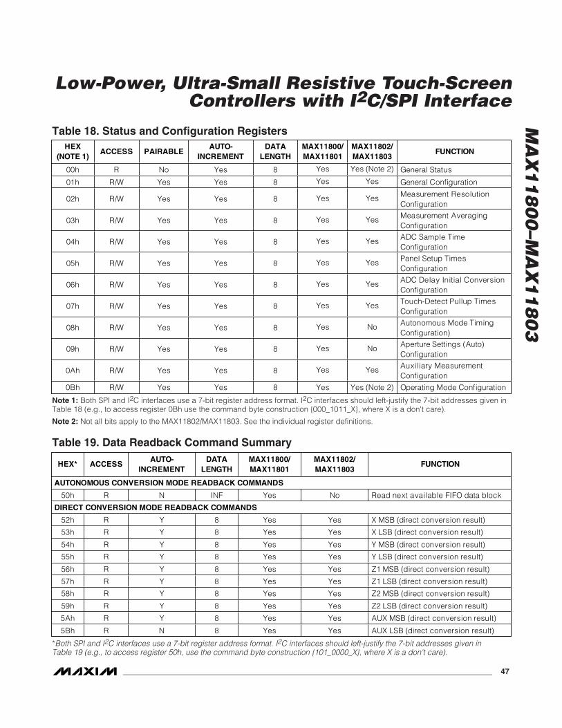
MA
X1
18
00
–MA
X1
18
03
Low-Power, Ultra-Small Resistive Touch-ScreenControllers with I2C/SPI Interface
______________________________________________________________________________________ 47
HEX* ACCESSAUTO-
INCREMENTDATA
LENGTHMAX11800/ MAX11801
MAX11802/ MAX11803
FUNCTION
AUTONOMOUS CONVERSION MODE READBACK COMMANDS
50h R N INF Yes No Read next available FIFO data block
DIRECT CONVERSION MODE READBACK COMMANDS
52h R Y 8 Yes Yes X MSB (direct conversion result)
53h R Y 8 Yes Yes X LSB (direct conversion result)
54h R Y 8 Yes Yes Y MSB (direct conversion result)
55h R Y 8 Yes Yes Y LSB (direct conversion result)
56h R Y 8 Yes Yes Z1 MSB (direct conversion result)
57h R Y 8 Yes Yes Z1 LSB (direct conversion result)
58h R Y 8 Yes Yes Z2 MSB (direct conversion result)
59h R Y 8 Yes Yes Z2 LSB (direct conversion result)
5Ah R Y 8 Yes Yes AUX MSB (direct conversion result)
5Bh R N 8 Yes Yes AUX LSB (direct conversion result)
Table 19. Data Readback Command Summary
*Both SPI and I2C interfaces use a 7-bit register address format. I2C interfaces should left-justify the 7-bit addresses given inTable 19 (e.g., to access register 50h, use the command byte construction {101_0000_X}, where X is a don't care).
HEX (NOTE 1)
ACCESS PAIRABLE AUTO-
INCREMENT DATA
LENGTH MAX11800/ MAX11801
MAX11802/MAX11803
FUNCTION
00h R No Yes 8 Yes Yes (Note 2) General Status
01h R/W Yes Yes 8 Yes Yes General Configuration
02h R/W Yes Yes 8 Yes Yes Measurement Resolution Configuration
03h R/W Yes Yes 8 Yes Yes Measurement Averaging Configuration
04h R/W Yes Yes 8 Yes Yes ADC Sample Time Configuration
05h R/W Yes Yes 8 Yes Yes Panel Setup Times Configuration
06h R/W Yes Yes 8 Yes Yes ADC Delay Initial Conversion Configuration
07h R/W Yes Yes 8 Yes Yes Touch-Detect Pullup Times Configuration
08h R/W Yes Yes 8 Yes No Autonomous Mode Timing Configuration)
09h R/W Yes Yes 8 Yes No Aperture Settings (Auto) Configuration
0Ah R/W Yes Yes 8 Yes Yes Auxiliary Measurement Configuration
0Bh R/W Yes Yes 8 Yes Yes (Note 2) Operating Mode Configuration
Table 18. Status and Configuration Registers
Note 1: Both SPI and I2C interfaces use a 7-bit register address format. I2C interfaces should left-justify the 7-bit addresses given inTable 18 (e.g., to access register 0Bh use the command byte construction {000_1011_X}, where X is a don't care).
Note 2: Not all bits apply to the MAX11802/MAX11803. See the individual register definitions.
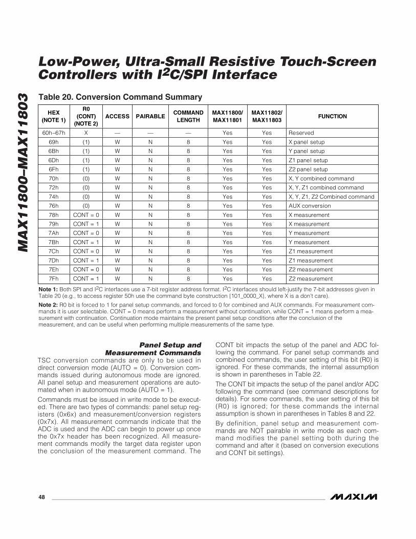
MA
X1
18
00
–MA
X1
18
03
Low-Power, Ultra-Small Resistive Touch-ScreenControllers with I2C/SPI Interface
48 ______________________________________________________________________________________
HEX (NOTE 1)
R0 (CONT)
(NOTE 2)ACCESS PAIRABLE
COMMAND LENGTH
MAX11800/ MAX11801
MAX11802/ MAX11803
FUNCTION
60h–67h X — — — Yes Yes Reserved
69h (1) W N 8 Yes Yes X panel setup
6Bh (1) W N 8 Yes Yes Y panel setup
6Dh (1) W N 8 Yes Yes Z1 panel setup
6Fh (1) W N 8 Yes Yes Z2 panel setup
70h (0) W N 8 Yes Yes X, Y combined command
72h (0) W N 8 Yes Yes X, Y, Z1 combined command
74h (0) W N 8 Yes Yes X, Y, Z1, Z2 Combined command
76h (0) W N 8 Yes Yes AUX conversion
78h CONT = 0 W N 8 Yes Yes X measurement
79h CONT = 1 W N 8 Yes Yes X measurement
7Ah CONT = 0 W N 8 Yes Yes Y measurement
7Bh CONT = 1 W N 8 Yes Yes Y measurement
7Ch CONT = 0 W N 8 Yes Yes Z1 measurement
7Dh CONT = 1 W N 8 Yes Yes Z1 measurement
7Eh CONT = 0 W N 8 Yes Yes Z2 measurement
7Fh CONT = 1 W N 8 Yes Yes Z2 measurement
Table 20. Conversion Command Summary
Panel Setup and Measurement Commands
TSC conversion commands are only to be used indirect conversion mode (AUTO = 0). Conversion com-mands issued during autonomous mode are ignored.All panel setup and measurement operations are auto-mated when in autonomous mode (AUTO = 1).
Commands must be issued in write mode to be execut-ed. There are two types of commands: panel setup reg-isters (0x6x) and measurement/conversion registers(0x7x). All measurement commands indicate that theADC is used and the ADC can begin to power up oncethe 0x7x header has been recognized. All measure-ment commands modify the target data register uponthe conclusion of the measurement command. The
CONT bit impacts the setup of the panel and ADC fol-lowing the command. For panel setup commands andcombined commands, the user setting of this bit (R0) isignored. For these commands, the internal assumptionis shown in parentheses in Table 22.
The CONT bit impacts the setup of the panel and/or ADCfollowing the command (see command descriptions fordetails). For some commands, the user setting of this bit(R0) is ignored; for these commands the internalassumption is shown in parentheses in Tables 8 and 22.
By definition, panel setup and measurement com-mands are NOT pairable in write mode as each com-mand modifies the panel setting both during thecommand and after it (based on conversion executionsand CONT bit settings).
Note 1: Both SPI and I2C interfaces use a 7-bit register address format. I2C interfaces should left-justify the 7-bit addresses given inTable 20 (e.g., to access register 50h use the command byte construction {101_0000_X}, where X is a don't care).
Note 2: R0 bit is forced to 1 for panel setup commands, and forced to 0 for combined and AUX commands. For measurement com-mands it is user selectable. CONT = 0 means perform a measurement without continuation, while CONT = 1 means perform a mea-surement with continuation. Continuation mode maintains the present panel setup conditions after the conclusion of themeasurement, and can be useful when performing multiple measurements of the same type.
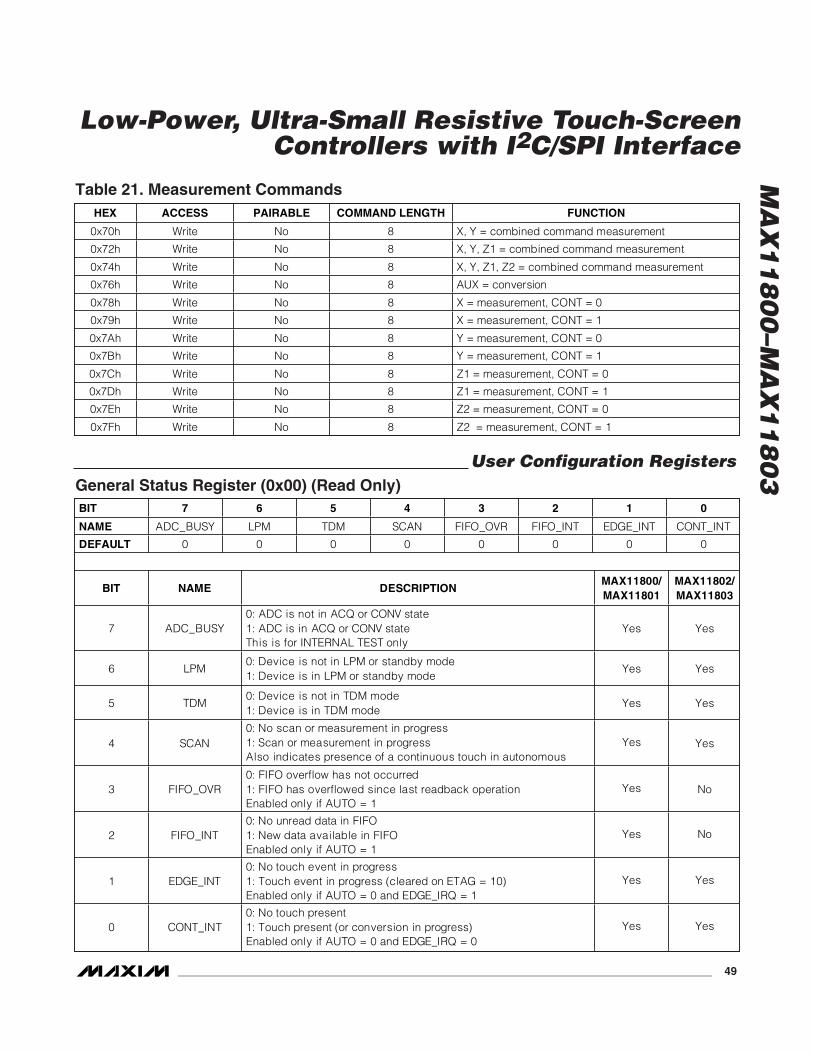
MA
X1
18
00
–MA
X1
18
03
Low-Power, Ultra-Small Resistive Touch-ScreenControllers with I2C/SPI Interface
______________________________________________________________________________________ 49
HEX ACCESS PAIRABLE COMMAND LENGTH FUNCTION
0x70h Write No 8 X, Y = combined command measurement
0x72h Write No 8 X, Y, Z1 = combined command measurement
0x74h Write No 8 X, Y, Z1, Z2 = combined command measurement
0x76h Write No 8 AUX = conversion
0x78h Write No 8 X = measurement, CONT = 0
0x79h Write No 8 X = measurement, CONT = 1
0x7Ah Write No 8 Y = measurement, CONT = 0
0x7Bh Write No 8 Y = measurement, CONT = 1
0x7Ch Write No 8 Z1 = measurement, CONT = 0
0x7Dh Write No 8 Z1 = measurement, CONT = 1
0x7Eh Write No 8 Z2 = measurement, CONT = 0
0x7Fh Write No 8 Z2 = measurement, CONT = 1
Table 21. Measurement Commands
BIT 7 6 5 4 3 2 1 0
NAME ADC_BUSY LPM TDM SCAN FIFO_OVR FIFO_INT EDGE_INT CONT_INT
DEFAULT 0 0 0 0 0 0 0 0
BIT NAME DESCRIPTIONMAX11800/ MAX11801
MAX11802/ MAX11803
7 ADC_BUSY 0: ADC is not in ACQ or CONV state 1: ADC is in ACQ or CONV state This is for INTERNAL TEST only
Yes Yes
6 LPM 0: Device is not in LPM or standby mode 1: Device is in LPM or standby mode
Yes Yes
5 TDM 0: Device is not in TDM mode 1: Device is in TDM mode
Yes Yes
4 SCAN 0: No scan or measurement in progress 1: Scan or measurement in progress Also indicates presence of a continuous touch in autonomous
Yes Yes
3 FIFO_OVR 0: FIFO overflow has not occurred 1: FIFO has overflowed since last readback operation Enabled only if AUTO = 1
Yes No
2 FIFO_INT 0: No unread data in FIFO 1: New data available in FIFO Enabled only if AUTO = 1
Yes No
1 EDGE_INT 0: No touch event in progress 1: Touch event in progress (cleared on ETAG = 10) Enabled only if AUTO = 0 and EDGE_IRQ = 1
Yes Yes
0 CONT_INT 0: No touch present 1: Touch present (or conversion in progress) Enabled only if AUTO = 0 and EDGE_IRQ = 0
Yes Yes
General Status Register (0x00) (Read Only)
User Configuration Registers
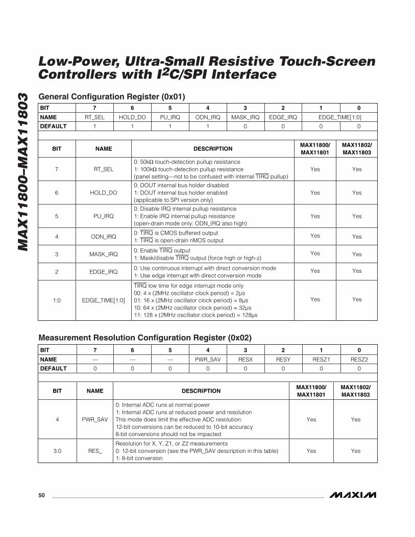
MA
X1
18
00
–MA
X1
18
03
Low-Power, Ultra-Small Resistive Touch-ScreenControllers with I2C/SPI Interface
50 ______________________________________________________________________________________
BIT 7 6 5 4 3 2 1 0
NAME — — — PWR_SAV RESX RESY RESZ1 RESZ2
DEFAULT 0 0 0 0 0 0 0 0
BIT NAME DESCRIPTIONMAX11800/ MAX11801
MAX11802/ MAX11803
4 PWR_SAV
0: Internal ADC runs at normal power 1: Internal ADC runs at reduced power and resolution This mode does limit the effective ADC resolution: 12-bit conversions can be reduced to 10-bit accuracy 8-bit conversions should not be impacted
Yes Yes
3:0 RES_ Resolution for X, Y, Z1, or Z2 measurements 0: 12-bit conversion (see the PWR_SAV description in this table) 1: 8-bit conversion
Yes Yes
Measurement Resolution Configuration Register (0x02)
BIT 7 6 5 4 3 2 1 0
NAME RT_SEL HOLD_DO PU_IRQ ODN_IRQ MASK_IRQ EDGE_IRQ EDGE_TIME[1:0]
DEFAULT 1 1 1 1 0 0 0 0
BIT NAME DESCRIPTIONMAX11800/ MAX11801
MAX11802/ MAX11803
7 RT_SEL 0: 50k touch-detection pullup resistance 1: 100k touch-detection pullup resistance (panel setting—not to be confused with internal TIRQ pullup)
Yes Yes
6 HOLD_DO 0: DOUT internal bus holder disabled 1: DOUT internal bus holder enabled (applicable to SPI version only)
Yes Yes
5 PU_IRQ 0: Disable IRQ internal pullup resistance 1: Enable IRQ internal pullup resistance (open-drain mode only: ODN_IRQ also high)
Yes Yes
4 ODN_IRQ 0: TIRQ is CMOS buffered output 1: TIRQ is open-drain nMOS output
Yes Yes
3 MASK_IRQ 0: Enable TIRQ output 1: Mask/disable TIRQ output (force high or high-z)
Yes Yes
2 EDGE_IRQ 0: Use continuous interrupt with direct conversion mode 1: Use edge interrupt with direct conversion mode
Yes Yes
1:0 EDGE_TIME[1:0]
TIRQ low time for edge interrupt mode only 00: 4 x (2MHz oscillator clock period) = 2μs 01: 16 x (2MHz oscillator clock period) = 8μs 10: 64 x (2MHz oscillator clock period) = 32μs 11: 128 x (2MHz oscillator clock period) = 128μs
Yes Yes
General Configuration Register (0x01)
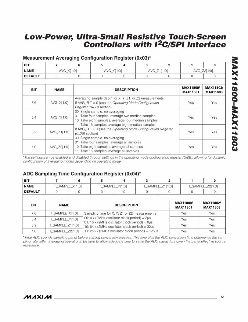
MA
X1
18
00
–MA
X1
18
03
Low-Power, Ultra-Small Resistive Touch-ScreenControllers with I2C/SPI Interface
______________________________________________________________________________________ 51
BIT 7 6 5 4 3 2 1 0
NAME T_SAMPLE_X[1:0] T_SAMPLE_Y[1:0] T_SAMPLE_Z1[1:0] T_SAMPLE_Z2[1:0]
DEFAULT 0 0 0 0 0 0 0 0
BIT NAME DESCRIPTIONMAX11800/ MAX11801
MAX11802/ MAX11803
7:6 T_SAMPLE_X[1:0] Yes Yes
5:4 T_SAMPLE_Y[1:0] Yes Yes
3:2 T_SAMPLE_Z1[1:0] Yes Yes
1:0 T_SAMPLE_Z2[1:0]
Sampling time for X, Y, Z1 or Z2 measurements 00: 4 x (2MHz oscillator clock period) = 2μs 01: 16 x (2MHz oscillator clock period) = 8μs 10: 64 x (2MHz oscillator clock period) = 32μs 11: 256 x (2MHz oscillator clock period) = 128μs Yes Yes
ADC Sampling Time Configuration Register (0x04)*
*Time ADC spends sampling panel before starting conversion process. This time plus the ADC conversion time determines the sam-pling rate within averaging operations. Be sure to allow adequate time to settle the ADC capacitors given the panel effective sourceresistance.
BIT 7 6 5 4 3 2 1 0
NAME AVG_X[1:0] AVG_Y[1:0] AVG_Z1[1:0] AVG_Z2[1:0]
DEFAULT 0 0 0 0 0 0 0 0
BIT NAME DESCRIPTIONMAX11800/ MAX11801
MAX11802/ MAX11803
7:6 AVG_X[1:0] Yes Yes
5:4 AVG_Y[1:0] Yes Yes
3:2 AVG_Z1[1:0] Yes Yes
1:0 AVG_Z2[1:0]
Averaging sample depth for X, Y, Z1, or Z2 measurements If AVG_FLT = 0 (see the Operating Mode Configuration Register (0x0B) section) 00: Single sample, no averaging 01: Take four samples, average two median samples 10: Take eight samples, average four median samples 11: Take 16 samples, average eight median samples If AVG_FLT = 1 (see the Operating Mode Configuration Register (0x0B) section) 00: Single sample, no averaging 01: Take four samples, average all samples 10: Take eight samples, average all samples 11: Take 16 samples, average all samples
Yes Yes
Measurement Averaging Configuration Register (0x03)*
*The settings can be enabled and disabled through settings in the operating mode configuration register (0x0B), allowing for dynamicconfiguration of averaging modes depending on operating mode.
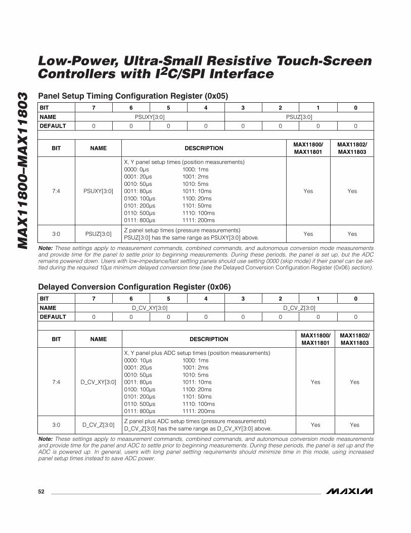
MA
X1
18
00
–MA
X1
18
03
Low-Power, Ultra-Small Resistive Touch-ScreenControllers with I2C/SPI Interface
52 ______________________________________________________________________________________
Note: These settings apply to measurement commands, combined commands, and autonomous conversion mode measurementsand provide time for the panel to settle prior to beginning measurements. During these periods, the panel is set up, but the ADCremains powered down. Users with low-impedance/fast settling panels should use setting 0000 (skip mode) if their panel can be set-tled during the required 10μs minimum delayed conversion time (see the Delayed Conversion Configuration Register (0x06) section).
BIT 7 6 5 4 3 2 1 0
NAME D_CV_XY[3:0] D_CV_Z[3:0]
DEFAULT 0 0 0 0 0 0 0 0
BIT NAME DESCRIPTIONMAX11800/ MAX11801
MAX11802/ MAX11803
7:4 D_CV_XY[3:0]
X, Y panel plus ADC setup times (position measurements) 0000: 10μs 1000: 1ms 0001: 20μs 1001: 2ms 0010: 50μs 1010: 5ms 0011: 80μs 1011: 10ms 0100: 100μs 1100: 20ms 0101: 200μs 1101: 50ms 0110: 500μs 1110: 100ms 0111: 800μs 1111: 200ms
Yes Yes
3:0 D_CV_Z[3:0] Z panel plus ADC setup times (pressure measurements) D_CV_Z[3:0] has the same range as D_CV_XY[3:0] above.
Yes Yes
Delayed Conversion Configuration Register (0x06)
Note: These settings apply to measurement commands, combined commands, and autonomous conversion mode measurementsand provide time for the panel and ADC to settle prior to beginning measurements. During these periods, the panel is set up and theADC is powered up. In general, users with long panel settling requirements should minimize time in this mode, using increasedpanel setup times instead to save ADC power.
BIT 7 6 5 4 3 2 1 0
NAME PSUXY[3:0] PSUZ[3:0]
DEFAULT 0 0 0 0 0 0 0 0
BIT NAME DESCRIPTIONMAX11800/ MAX11801
MAX11802/ MAX11803
7:4 PSUXY[3:0]
X, Y panel setup times (position measurements) 0000: 0μs 1000: 1ms 0001: 20μs 1001: 2ms 0010: 50μs 1010: 5ms 0011: 80μs 1011: 10ms 0100: 100μs 1100: 20ms 0101: 200μs 1101: 50ms 0110: 500μs 1110: 100ms 0111: 800μs 1111: 200ms
Yes Yes
3:0 PSUZ[3:0] Z panel setup times (pressure measurements) PSUZ[3:0] has the same range as PSUXY[3:0] above.
Yes Yes
Panel Setup Timing Configuration Register (0x05)
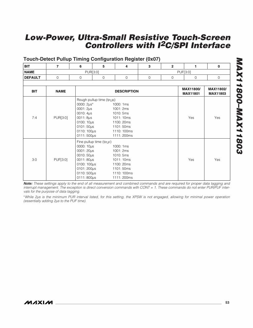
MA
X1
18
00
–MA
X1
18
03
Low-Power, Ultra-Small Resistive Touch-ScreenControllers with I2C/SPI Interface
______________________________________________________________________________________ 53
Note: These settings apply to the end of all measurement and combined commands and are required for proper data tagging andinterrupt management. The exception is direct conversion commands with CONT = 1. These commands do not enter PUR/PUF inter-vals for the purpose of data tagging.
*While 2μs is the minimum PUR interval listed, for this setting, the XPSW is not engaged, allowing for minimal power operation(essentially adding 2μs to the PUF time).
BIT 7 6 5 4 3 2 1 0
NAME PUR[3:0] PUF[3:0]
DEFAULT 0 0 0 0 0 0 0 0
BIT NAME DESCRIPTIONMAX11800/ MAX11801
MAX11802/ MAX11803
7:4 PUR[3:0]
Rough pullup time (tPUR)0000: 2μs* 1000: 1ms 0001: 2μs 1001: 2ms 0010: 4μs 1010: 5ms 0011: 8μs 1011: 10ms 0100: 10μs 1100: 20ms 0101: 50μs 1101: 50ms 0110: 100μs 1110: 100ms 0111: 500μs 1111: 200ms
Yes Yes
3:0 PUF[3:0]
Fine pullup time (tPUF)0000: 10μs 1000: 1ms 0001: 20μs 1001: 2ms 0010: 50μs 1010: 5ms 0011: 80μs 1011: 10ms 0100: 100μs 1100: 20ms 0101: 200μs 1101: 50ms 0110: 500μs 1110: 100ms 0111: 800μs 1111: 200ms
Yes Yes
Touch-Detect Pullup Timing Configuration Register (0x07)
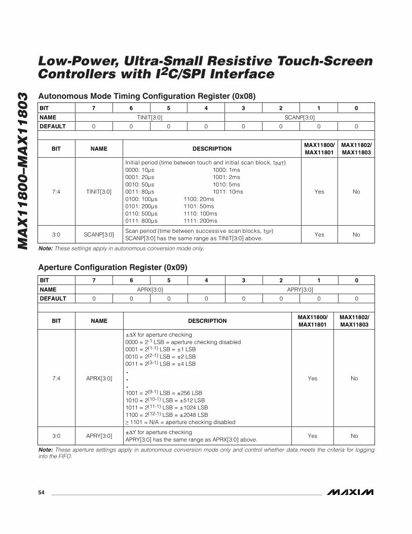
MA
X1
18
00
–MA
X1
18
03
Low-Power, Ultra-Small Resistive Touch-ScreenControllers with I2C/SPI Interface
54 ______________________________________________________________________________________
BIT 7 6 5 4 3 2 1 0
NAME APRX[3:0] APRY[3:0]
DEFAULT 0 0 0 0 0 0 0 0
BIT NAME DESCRIPTIONMAX11800/ MAX11801
MAX11802/ MAX11803
7:4 APRX[3:0]
± X for aperture checking 0000 = 2-1 LSB = aperture checking disabled 0001 = 2(1-1) LSB = ±1 LSB 0010 = 2(2-1) LSB = ±2 LSB 0011 = 2(3-1) LSB = ±4 LSB ...1001 = 2(9-1) LSB = ±256 LSB 1010 = 2(10-1) LSB = ±512 LSB 1011 = 2(11-1) LSB = ±1024 LSB 1100 = 2(12-1) LSB = ±2048 LSB
1101 = N/A = aperture checking disabled
Yes No
3:0 APRY[3:0] ± Y for aperture checking APRY[3:0] has the same range as APRX[3:0] above.
Yes No
Aperture Configuration Register (0x09)
Note: These aperture settings apply in autonomous conversion mode only and control whether data meets the criteria for logginginto the FIFO.
BIT 7 6 5 4 3 2 1 0
NAME TINIT[3:0] SCANP[3:0]
DEFAULT 0 0 0 0 0 0 0 0
BIT NAME DESCRIPTIONMAX11800/ MAX11801
MAX11802/ MAX11803
7:4 TINIT[3:0]
Initial period (time between touch and initial scan block, tINIT)0000: 10μs 1000: 1ms 0001: 20μs 1001: 2ms 0010: 50μs 1010: 5ms 0011: 80μs 1011: 10ms 0100: 100μs 1100: 20ms 0101: 200μs 1101: 50ms 0110: 500μs 1110: 100ms 0111: 800μs 1111: 200ms
Yes No
3:0 SCANP[3:0] Scan period (time between successive scan blocks, tSP)SCANP[3:0] has the same range as TINIT[3:0] above.
Yes No
Autonomous Mode Timing Configuration Register (0x08)
Note: These settings apply in autonomous conversion mode only.
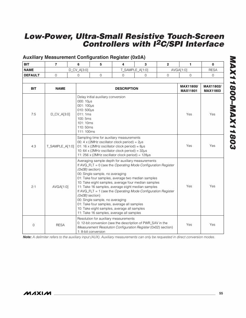
MA
X1
18
00
–MA
X1
18
03
Low-Power, Ultra-Small Resistive Touch-ScreenControllers with I2C/SPI Interface
______________________________________________________________________________________ 55
BIT 7 6 5 4 3 2 1 0
NAME D_CV_A[3:0] T_SAMPLE_A[1:0] AVGA[1:0] RESA
DEFAULT 0 0 0 0 0 0 0 0
BIT NAME DESCRIPTIONMAX11800/ MAX11801
MAX11802/ MAX11803
7:5 D_CV_A[3:0]
Delay initial auxiliary conversion 000: 10μs 001: 100μs 010: 500μs 011: 1ms 100: 5ms 101: 10ms 110: 50ms 111: 100ms
Yes Yes
4:3 T_SAMPLE_A[1:0]
Sampling time for auxiliary measurements 00: 4 x (2MHz oscillator clock period) = 2μs 01: 16 x (2MHz oscillator clock period) = 8μs 10: 64 x (2MHz oscillator clock period) = 32μs 11: 256 x (2MHz oscillator clock period) = 128μs
Yes Yes
2:1 AVGA[1:0]
Averaging sample depth for auxiliary measurements If AVG_FLT = 0 (see the Operating Mode Configuration Register (0x0B) section)00: Single sample, no averaging 01: Take four samples, average two median samples 10: Take eight samples, average four median samples 11: Take 16 samples, average eight median samples If AVG_FLT = 1 (see the Operating Mode Configuration Register (0x0B) section) 00: Single sample, no averaging 01: Take four samples, average all samples 10: Take eight samples, average all samples 11: Take 16 samples, average all samples
Yes Yes
0 RESA
Resolution for auxiliary measurements 0: 12-bit conversion (see the description of PWR_SAV in the Measurement Resolution Configuration Register (0x02) section) 1: 8-bit conversion
Yes Yes
Auxiliary Measurement Configuration Register (0x0A)
Note: A delimiter refers to the auxiliary input (AUX). Auxiliary measurements can only be requested in direct conversion modes.
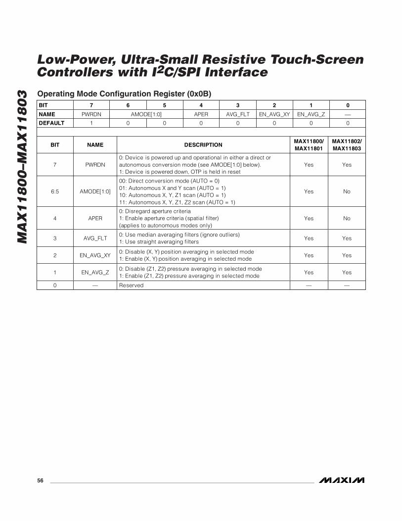
MA
X1
18
00
–MA
X1
18
03
Low-Power, Ultra-Small Resistive Touch-ScreenControllers with I2C/SPI Interface
56 ______________________________________________________________________________________
BIT 7 6 5 4 3 2 1 0
NAME PWRDN AMODE[1:0] APER AVG_FLT EN_AVG_XY EN_AVG_Z
DEFAULT 1 0 0 0 0 0 0 0
BIT NAME DESCRIPTIONMAX11800/ MAX11801
MAX11802/ MAX11803
7 PWRDN 0: Device is powered up and operational in either a direct or autonomous conversion mode (see AMODE[1:0] below). 1: Device is powered down, OTP is held in reset
Yes Yes
6:5 AMODE[1:0]
00: Direct conversion mode (AUTO = 0) 01: Autonomous X and Y scan (AUTO = 1) 10: Autonomous X, Y, Z1 scan (AUTO = 1) 11: Autonomous X, Y, Z1, Z2 scan (AUTO = 1)
Yes No
4 APER 0: Disregard aperture criteria 1: Enable aperture criteria (spatial filter) (applies to autonomous modes only)
Yes No
3 AVG_FLT 0: Use median averaging filters (ignore outliers) 1: Use straight averaging filters
Yes Yes
2 EN_AVG_XY 0: Disable (X, Y) position averaging in selected mode 1: Enable (X, Y) position averaging in selected mode
Yes Yes
1 EN_AVG_Z 0: Disable (Z1, Z2) pressure averaging in selected mode 1: Enable (Z1, Z2) pressure averaging in selected mode
Yes Yes
0 — Reserved — —
Operating Mode Configuration Register (0x0B)
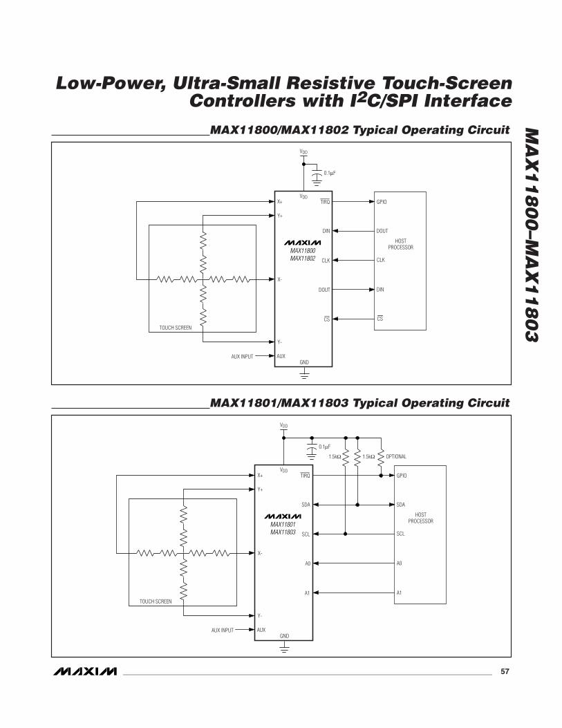
MA
X1
18
00
–MA
X1
18
03
Low-Power, Ultra-Small Resistive Touch-ScreenControllers with I2C/SPI Interface
______________________________________________________________________________________ 57
TOUCH SCREEN
X+
Y+
X-
Y-
GPIO
0.1μF
DOUT
CLK
DIN
CS
VDD
VDDTIRQ
DIN
CLK
DOUT
CS
GNDAUXAUX INPUT
HOSTPROCESSORMAX11800
MAX11802
TOUCH SCREEN
X+
Y+
X-
Y-
GPIO
1.5kΩ 1.5kΩ
SDA
SCL
A0
A1
VDD
VDDTIRQ
SDA
SCL
A0
A1
GNDAUXAUX INPUT
HOSTPROCESSORMAX11801
MAX11803
0.1μF
OPTIONAL
MAX11801/MAX11803 Typical Operating Circuit
MAX11800/MAX11802 Typical Operating Circuit
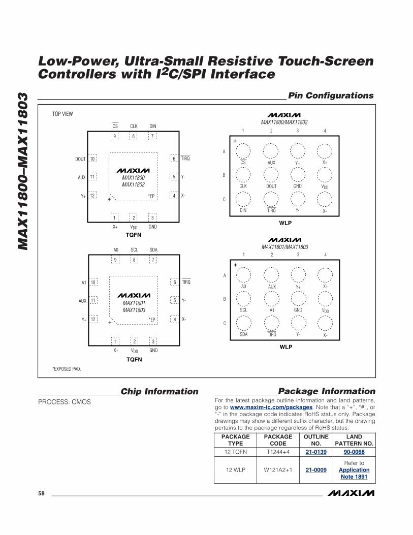
MA
X1
18
00
–MA
X1
18
03
Low-Power, Ultra-Small Resistive Touch-ScreenControllers with I2C/SPI Interface
58 ______________________________________________________________________________________
Package InformationFor the latest package outline information and land patterns,go to www.maxim-ic.com/packages. Note that a “+”, “#”, or“-” in the package code indicates RoHS status only. Packagedrawings may show a different suffix character, but the drawingpertains to the package regardless of RoHS status.
Chip InformationPROCESS: CMOS
AUX
X-
CS
Y-
DOUT VDDCLK GND
2 41 3
TIRQ
X+
DIN
A
B
C
Y+
MAX11800/MAX11802
+
WLP
TOP VIEW
AUX
X-
A0
Y-
A1 VDDSCL GND
2 41 3
TIRQ
X+
SDA
A
B
C
Y+
MAX11801/MAX11803
TQFN
+
+
WLP
12
11
10
4
5
6
1 2
AUX
3
9 8 7
Y+
TIRQ
Y-
X-
MAX11801MAX11803
A1
X+ VDD GND
A0 SCL SDA
12
11
10
4
5
6
1 2
AUX
3
9 8 7
Y+
TIRQ
Y-
X-
MAX11800MAX11802
DOUT
X+ VDD GND
CS CLK DIN
*EP
TQFN
+
*EP
*EXPOSED PAD.
Pin Configurations
PACKAGETYPE
PACKAGECODE
OUTLINENO.
LANDPATTERN NO.
12 TQFN T1244+4 21-0139 90-0068
12 WLP W121A2+1 21-0009Refer to
ApplicationNote 1891
MA
X1
18
00
–MA
X1
18
03
Low-Power, Ultra-Small Resistive Touch-ScreenControllers with I2C/SPI Interface
Maxim cannot assume responsibility for use of any circuitry other than circuitry entirely embodied in a Maxim product. No circuit patent licenses areimplied. Maxim reserves the right to change the circuitry and specifications without notice at any time.
Maxim Integrated Products, 120 San Gabriel Drive, Sunnyvale, CA 94086 408-737-7600 ____________________ 59
© 2010 Maxim Integrated Products Maxim is a registered trademark of Maxim Integrated Products, Inc.
Revision HistoryREVISION NUMBER
REVISION DATE
DESCRIPTION PAGES
CHANGED
0 7/09 Initial release —
Removed future status from the WLP packages in the Ordering Information table. 1
Added a new Note 1 about the WLP package to the Absolute Maximum Ratingssection.
81 11/09
Corrected the pin names for the WLP packages in the Pin Description table and Pin Configurations.
14, 56
2 3/10 Added “Soldering Temperature (reflow) at +260°C.” in the Absolute Maximum Ratings section.
8
3 10/10 Added information to differentiate the MAX11800/MAX11801 features and operating modes from the MAX11802/MAX11803 features and operating modes.
All


![Identify Audience RFA 2015[2] · 2017-04-18 · Action Plan 1 Messenger Mode/Tools Date(s) Desired Outcome Outcome Follow-up Touch 1 Touch 2 Touch 3 Determine and outline how you](https://img.pdfslide.us/doc/110x75/5e8b3551ba1b4a20791efb21/identify-audience-rfa-20152-2017-04-18-action-plan-1-messenger-modetools-dates.jpg)