Embed Size (px)
Citation preview
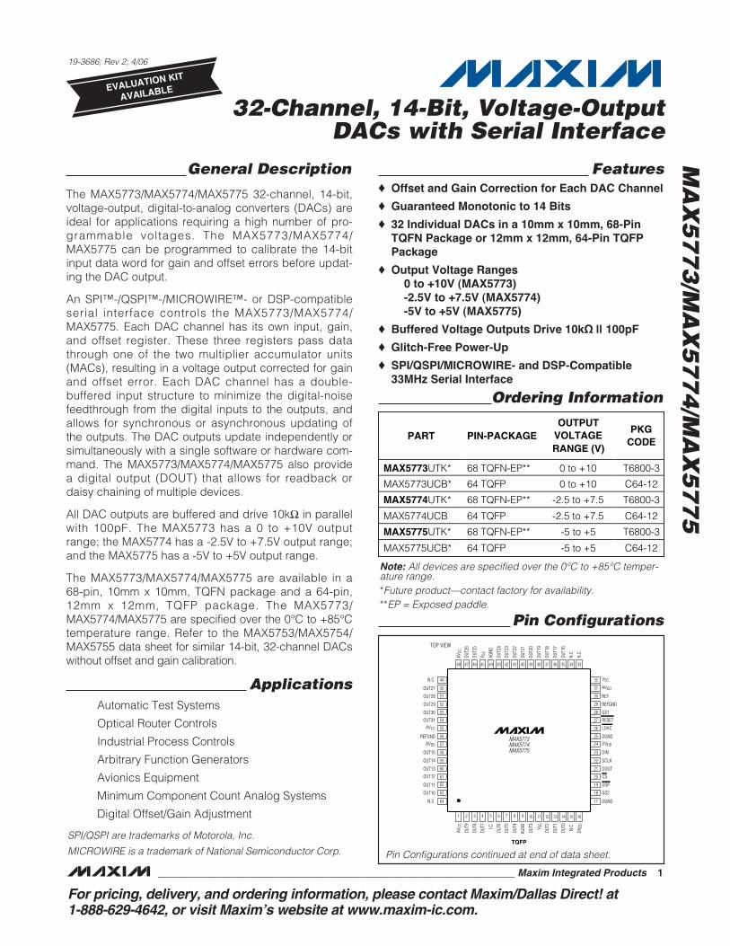
General Description
The MAX5773/MAX5774/MAX5775 32-channel, 14-bit,voltage-output, digital-to-analog converters (DACs) areideal for applications requiring a high number of pro-grammable voltages. The MAX5773/MAX5774/MAX5775 can be programmed to calibrate the 14-bitinput data word for gain and offset errors before updat-ing the DAC output.
An SPI™-/QSPI™-/MICROWIRE™- or DSP-compatibleserial interface controls the MAX5773/MAX5774/MAX5775. Each DAC channel has its own input, gain,and offset register. These three registers pass datathrough one of the two multiplier accumulator units(MACs), resulting in a voltage output corrected for gainand offset error. Each DAC channel has a double-buffered input structure to minimize the digital-noisefeedthrough from the digital inputs to the outputs, andallows for synchronous or asynchronous updating ofthe outputs. The DAC outputs update independently orsimultaneously with a single software or hardware com-mand. The MAX5773/MAX5774/MAX5775 also providea digital output (DOUT) that allows for readback ordaisy chaining of multiple devices.
All DAC outputs are buffered and drive 10kΩ in parallelwith 100pF. The MAX5773 has a 0 to +10V outputrange; the MAX5774 has a -2.5V to +7.5V output range;and the MAX5775 has a -5V to +5V output range.
The MAX5773/MAX5774/MAX5775 are available in a68-pin, 10mm x 10mm, TQFN package and a 64-pin,12mm x 12mm, TQFP package. The MAX5773/MAX5774/MAX5775 are specified over the 0°C to +85°Ctemperature range. Refer to the MAX5753/MAX5754/MAX5755 data sheet for similar 14-bit, 32-channel DACswithout offset and gain calibration.
ApplicationsAutomatic Test Systems
Optical Router Controls
Industrial Process Controls
Arbitrary Function Generators
Avionics Equipment
Minimum Component Count Analog Systems
Digital Offset/Gain Adjustment
Features Offset and Gain Correction for Each DAC Channel
Guaranteed Monotonic to 14 Bits
32 Individual DACs in a 10mm x 10mm, 68-PinTQFN Package or 12mm x 12mm, 64-Pin TQFPPackage
Output Voltage Ranges0 to +10V (MAX5773)-2.5V to +7.5V (MAX5774)-5V to +5V (MAX5775)
Buffered Voltage Outputs Drive 10kΩ || 100pF
Glitch-Free Power-Up
SPI/QSPI/MICROWIRE- and DSP-Compatible33MHz Serial Interface
MA
X5
77
3/M
AX
57
74
/MA
X5
77
5
32-Channel, 14-Bit, Voltage-OutputDACs with Serial Interface
________________________________________________________________ Maxim Integrated Products 1
Ordering Information
19-3686; Rev 2; 4/06
For pricing, delivery, and ordering information, please contact Maxim/Dallas Direct! at 1-888-629-4642, or visit Maxim’s website at www.maxim-ic.com.
EVALUATION KIT
AVAILABLE
PART PIN-PACKAGEOUTPUT
VOLTAGERANGE (V)
PKGCODE
MAX5773UTK* 68 TQFN-EP** 0 to +10 T6800-3
MAX5773UCB* 64 TQFP 0 to +10 C64-12
MAX5774UTK* 68 TQFN-EP** -2.5 to +7.5 T6800-3
MAX5774UCB 64 TQFP -2.5 to +7.5 C64-12
MAX5775UTK* 68 TQFN-EP** -5 to +5 T6800-3
MAX5775UCB* 64 TQFP -5 to +5 C64-12
Note: All devices are specified over the 0°C to +85°C temper-ature range.*Future product—contact factory for availability.**EP = Exposed paddle.
SPI/QSPI are trademarks of Motorola, Inc.
MICROWIRE is a trademark of National Semiconductor Corp.
58
59
60
61
62
54
55
56
57
63
38394041424344454647
V SS
DSP
OUT10
TQFP
TOP VIEW
OUT11
OUT12
OUT13
OUT14
OUT15
AVDD
REFGND
AVCC
OUT31
52
53
49
50
51
OUT30
OUT29
OUT28
OUT27
N.C.
GS2
DOUT
CS
DIN
SCLK
DGNDDVDD
RESET
LDAC
REFGND
GS1
AVDD
REF
VSS
OUT2
6
OUT2
5
V SS
AGND
OUT2
4
OUT2
3
OUT2
2
OUT2
1
OUT2
0
OUT1
9
3334353637
OUT1
8
OUT1
7
OUT1
6
N.C.
N.C.
OUT3
AGND
OUT4
OUT5
OUT6
DVDD
N.C.
OUT0
OUT1
OUT2I.C
.
OUT7
OUT8
OUT9
48
AVCC
AVCC
64N.C. DGND
23
22
21
20
19
27
26
25
24
18
29
28
32
31
30
17
111098765432 16151413121
MAX5773MAX5774MAX5775
Pin Configurations
Pin Configurations continued at end of data sheet.
MA
X5
77
3/M
AX
57
74
/MA
X5
77
5
32-Channel, 14-Bit, Voltage-OutputDACs with Serial Interface
2 _______________________________________________________________________________________
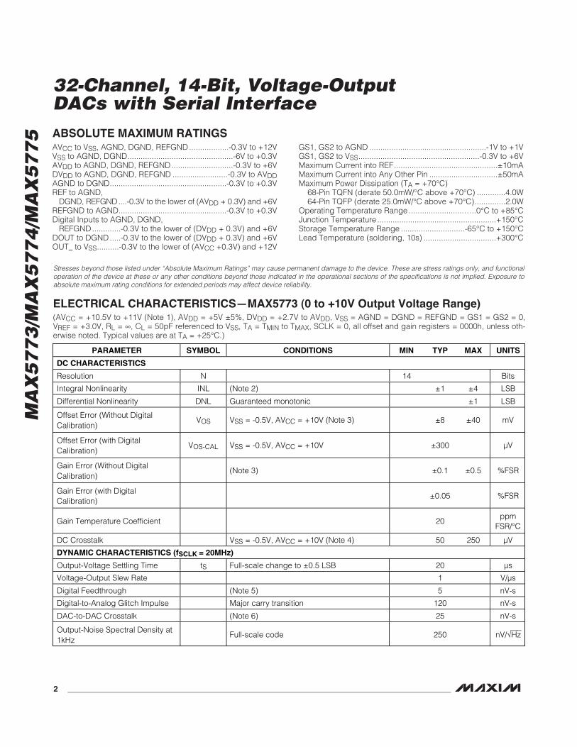
ABSOLUTE MAXIMUM RATINGS
Stresses beyond those listed under “Absolute Maximum Ratings” may cause permanent damage to the device. These are stress ratings only, and functionaloperation of the device at these or any other conditions beyond those indicated in the operational sections of the specifications is not implied. Exposure toabsolute maximum rating conditions for extended periods may affect device reliability.
AVCC to VSS, AGND, DGND, REFGND..................-0.3V to +12VVSS to AGND, DGND................................................-6V to +0.3VAVDD to AGND, DGND, REFGND............................-0.3V to +6VDVDD to AGND, DGND, REFGND .........................-0.3V to AVDDAGND to DGND.....................................................-0.3V to +0.3VREF to AGND,
DGND, REFGND....-0.3V to the lower of (AVDD + 0.3V) and +6VREFGND to AGND.................................................-0.3V to +0.3VDigital Inputs to AGND, DGND,
REFGND.............-0.3V to the lower of (DVDD + 0.3V) and +6VDOUT to DGND.....-0.3V to the lower of (DVDD + 0.3V) and +6VOUT_ to VSS..........-0.3V to the lower of (AVCC +0.3V) and +12V
GS1, GS2 to AGND .....................................................-1V to +1V GS1, GS2 to VSS.......................................................-0.3V to +6VMaximum Current into REF...............................................±10mAMaximum Current into Any Other Pin ...............................±50mAMaximum Power Dissipation (TA = +70°C)
68-Pin TQFN (derate 50.0mW/°C above +70°C) .............4.0W64-Pin TQFP (derate 25.0mW/°C above +70°C)..............2.0W
Operating Temperature Range .........................…..0°C to +85°CJunction Temperature ......................................................+150°CStorage Temperature Range .............................-65°C to +150°CLead Temperature (soldering, 10s) .................................+300°C
ELECTRICAL CHARACTERISTICS—MAX5773 (0 to +10V Output Voltage Range)(AVCC = +10.5V to +11V (Note 1), AVDD = +5V ±5%, DVDD = +2.7V to AVDD, VSS = AGND = DGND = REFGND = GS1 = GS2 = 0,VREF = +3.0V, RL = ∞, CL = 50pF referenced to VSS, TA = TMIN to TMAX, SCLK = 0, all offset and gain registers = 0000h, unless oth-erwise noted. Typical values are at TA = +25°C.)
PARAMETER SYMBOL CONDITIONS MIN TYP MAX UNITS
DC CHARACTERISTICS
Resolution N 14 Bits
Integral Nonlinearity INL (Note 2) ±1 ±4 LSB
Differential Nonlinearity DNL Guaranteed monotonic ±1 LSB
Offset Error (Without DigitalCalibration)
VOS VSS = -0.5V, AVCC = +10V (Note 3) ±8 ±40 mV
Offset Error (with DigitalCalibration)
VOS-CAL VSS = -0.5V, AVCC = +10V ±300 µV
Gain Error (Without DigitalCalibration)
(Note 3) ±0.1 ±0.5 %FSR
Gain Error (with DigitalCalibration)
±0.05 %FSR
Gain Temperature Coefficient 20ppm
FSR/°C
DC Crosstalk VSS = -0.5V, AVCC = +10V (Note 4) 50 250 µV
DYNAMIC CHARACTERISTICS (fSCLK = 20MHz)
Output-Voltage Settling Time tS Full-scale change to ±0.5 LSB 20 µs
Voltage-Output Slew Rate 1 V/µs
Digital Feedthrough (Note 5) 5 nV-s
Digital-to-Analog Glitch Impulse Major carry transition 120 nV-s
DAC-to-DAC Crosstalk (Note 6) 25 nV-s
Output-Noise Spectral Density at1kHz
Full-scale code 250 nV/√Hz

MA
X5
77
3/M
AX
57
74
/MA
X5
77
5
32-Channel, 14-Bit, Voltage-OutputDACs with Serial Interface
_______________________________________________________________________________________ 3
ELECTRICAL CHARACTERISTICS—MAX5773 (0 to +10V Output Voltage Range)(continued)(AVCC = +10.5V to +11V (Note 1), AVDD = +5V ±5%, DVDD = +2.7V to AVDD, VSS = AGND = DGND = REFGND = GS1 = GS2 = 0,VREF = +3.0V, RL = ∞, CL = 50pF referenced to VSS, TA = TMIN to TMAX, SCLK = 0, all offset and gain registers = 0000h, unless oth-erwise noted. Typical values are at TA = +25°C.)
PARAMETER SYMBOL CONDITIONS MIN TYP MAX UNITS
ANALOG OUTPUTS (OUT0 to OUT31)
Output-Voltage Range VSS = -0.5V, AVCC = +10.5V (Note 1) 0 10 V
Resistive Load to Ground 10 50 kΩCapacitive Load to Ground 100 pF
DC-Output Impedance 0.1 Ω
Sourcing, full scale, output connected toAGND
+5
Short-Circuit CurrentSinking, zero scale, output connected toAVCC
-5
mA
GROUND-SENSE ANALOG INPUTS (GS1 and GS2)
Input-Voltage Range VGS Relative to AGND -0.5 +0.5 V
Ground-Sense Gain AGS 0.995 1.000 1.005 V/V
Input Resistance -0.5V ≤ VGS ≤ +0.5V, VSS = -0.5V 70 kΩREFERENCE INPUT (REF)
Input Resistance 1 MΩReference Input Voltage Range VREF Referred to REFGND 2.900 3.000 3.100 V
DIGITAL INPUTS (CS, SCLK, DIN, LDAC, RESET, DSP)
+2.7V ≤ DVDD ≤ + 3.6V0.7 xDVDDInput-Voltage High VIH
+3.6V < DVDD ≤ +5.25V 2.4V
Input-Voltage Low VIL 0.8 V
Input Capacitance CIN 10 pF
Input Current IIN Digital inputs = 0 or DVDD ±1 µA
DIGITAL OUTPUT (DOUT)
Output-Voltage Low VOL ISINK = 1mA 0.4 V
Output-Voltage High VOH ISOURCE = 0.2mA0.8 xDVDD
V
Tri-State Leakage Current IL ±10 µA
Tri-State Output Capacitance COUT 10 pF
POWER REQUIREMENTS (AVCC, VSS, AGND, AVDD, DVDD, DGND)
Output-Amplifier Positive SupplyVoltage
AVCC 10 11 V
Output-Amplifier Negative SupplyVoltage
VSS -0.5 0 V
Output-Amplifier Supply VoltageDifference
AVCC - VSS 11 V
Analog Supply Voltage AVDD 4.75 5.25 V
Digital Supply Voltage DVDD 2.7 AVDD V

MA
X5
77
3/M
AX
57
74
/MA
X5
77
5
32-Channel, 14-Bit, Voltage-OutputDACs with Serial Interface
4 _______________________________________________________________________________________
ELECTRICAL CHARACTERISTICS—MAX5773 (0 to +10V Output Voltage Range)(continued)(AVCC = +10.5V to +11V (Note 1), AVDD = +5V ±5%, DVDD = +2.7V to AVDD, VSS = AGND = DGND = REFGND = GS1 = GS2 = 0,VREF = +3.0V, RL = ∞, CL = 50pF referenced to VSS, TA = TMIN to TMAX, SCLK = 0, all offset and gain registers = 0000h, unless oth-erwise noted. Typical values are at TA = +25°C.)
PARAMETER SYMBOL CONDITIONS MIN TYP MAX UNITS
VOUT0 through VOUT31 = 0 10 15 mAAnalog Supply Current AIDD
Software shutdown 10 µA
DVDD = +5V, VIH = DVDD, VIL = 0,fSCLK = 20MHz, continuous writethrough
2.5 3.5
DVDD = +5V, VIH = +2.4V, VIL = +0.8V,fSCLK = 20MHz, continuous writethrough
5.0 6.5
mADigital Supply Current DIDD
Software shutdown 75 nA
VOUT0 through VOUT31 = 0 4 10 mAOutput-Amplifier Positive SupplyCurrent
AICCSoftware shutdown 20 µA
VOUT0 throughVOUT31 = 0
-4 -10 mAOutput-Amplifier Negative SupplyCurrent
ISS VSS = -0.5V
Software shutdown -20 µA
Power-Supply Rejection Ratio PSRR -95 dB
ELECTRICAL CHARACTERISTICS—MAX5774 (-2.5V to +7.5V Output Voltage Range)(AVCC = +7.75V to +8.25V (Note 1), AVDD = +5V ±5%, DVDD = +2.7V to AVDD, VSS = -2.75V to -3.25V, AGND = DGND = REFGND= GS1 = GS2 = 0, program the offset DAC to 1000h. VREF = +3.0V, RL = ∞, CL= 50pF referenced to VSS, TA = TMIN to TMAX, SCLK =0, all offset and gain registers = 0000h, unless otherwise noted. Typical values are at TA = +25°C.)
PARAMETER SYMBOL CONDITIONS MIN TYP MAX UNITS
DC CHARACTERISTICS
Resolution N 14 Bits
Integral Nonlinearity INL (Note 2) ±1 ±4 LSB
Differential Nonlinearity DNL Guaranteed monotonic ±1 LSB
Offset Error (Without DigitalCalibration)
VOS VSS = -3.25V, AVCC = +7.75V (Note 3) ±8 ±40 mV
Offset Error (with DigitalCalibration)
VOS-CAL VSS = -3.25V, AVCC = +7.75V ±300 µV
Gain Error (Without DigitalCalibration)
(Note 3) ±0.1 ±0.5 %FSR
Gain Error (with DigitalCalibration)
±0.05 %FSR
Gain Temperature Coefficient 20ppm
FSR/°C
DC Crosstalk VSS = -3.25V, AVCC = +7.75V (Note 4) 50 250 µV
DYNAMIC CHARACTERISTICS (fSCLK = 20MHz)
Output-Voltage Settling Time tS Full-scale change to ±0.5 LSB 20 µs
Voltage-Output Slew Rate 1 V/µs
Digital Feedthrough (Note 5) 5 nV-s

MA
X5
77
3/M
AX
57
74
/MA
X5
77
5
32-Channel, 14-Bit, Voltage-OutputDACs with Serial Interface
_______________________________________________________________________________________ 5
ELECTRICAL CHARACTERISTICS—MAX5774 (-2.5V to +7.5V Output Voltage Range)(continued)(AVCC = +7.75V to +8.25V (Note 1), AVDD = +5V ±5%, DVDD = +2.7V to AVDD, VSS = -2.75V to -3.25V, AGND = DGND = REFGND= GS1 = GS2 = 0, program the offset DAC to 1000h. VREF = +3.0V, RL = ∞, CL= 50pF referenced to VSS, TA = TMIN to TMAX, SCLK =0, all offset and gain registers = 0000h, unless otherwise noted. Typical values are at TA = +25°C.)
PARAMETER SYMBOL CONDITIONS MIN TYP MAX UNITS
Digital-to-Analog Glitch Impulse Major carry transition 120 nV-s
DAC-to-DAC Crosstalk (Note 6) 25 nV-s
Output-Noise Spectral Density at1kHz
Full-scale code 250 nV/√Hz
ANALOG OUTPUTS (OUT0 to OUT31)
Output Voltage Range VSS = -2.75V, AVCC = +7.75V (Note 1) -2.5 +7.5 V
Resistive Load to Ground 10 50 kΩCapacitive Load to Ground 100 pF
DC Output Impedance 0.1 Ω
Sourcing, full scale, output connected toAGND
+5
Short-Circuit CurrentSinking, zero scale, output connected toAVCC
-5
mA
GROUND-SENSE ANALOG INPUTS (GS1 and GS2)
Input-Voltage Range VGS Relative to AGND -0.5 +0.5 V
Ground-Sense Gain AGS 0.993 1.000 1.005 V/V
Input Resistance -0.5V ≤ VGS ≤ +0.5V, VSS = -2.75V 70 kΩREFERENCE INPUT (REF)
Input Resistance 1 MΩReference Input Voltage Range VREF Referred to REFGND 2.900 3.000 3.100 V
DIGITAL INPUTS (CS, SCLK, DIN, LDAC, RESET, DSP)
+2.7V ≤ DVDD ≤ +3.6V0.7 xDVDDInput-Voltage High VIH
+3.6V < DVDD ≤ +5.25V 2.4
V
Input-Voltage Low VIL 0.8 V
Input Capacitance CIN 10 pF
Input Current IIN Digital inputs = 0 or DVDD ±1 µA
DIGITAL OUTPUT (DOUT)
Output-Voltage Low VOL ISINK = 1mA 0.4 V
Output-Voltage High VOH ISOURCE = 0.2mA0.8 xDVDD
V
Tri-State Leakage Current IL ±10 µA
Tri-State Output Capacitance COUT 10 pF
POWER REQUIREMENTS (AVCC, VSS, AGND, AVDD, DVDD, DGND)
Output-Amplifier Positive SupplyVoltage
AVCC 7.50 8.25 V

MA
X5
77
3/M
AX
57
74
/MA
X5
77
5
32-Channel, 14-Bit, Voltage-OutputDACs with Serial Interface
6 _______________________________________________________________________________________
ELECTRICAL CHARACTERISTICS—MAX5774 (-2.5V to +7.5V Output Voltage Range)(continued)(AVCC = +7.75V to +8.25V (Note 1), AVDD = +5V ±5%, DVDD = +2.7V to AVDD, VSS = -2.75V to -3.25V, AGND = DGND = REFGND= GS1 = GS2 = 0, program the offset DAC to 1000h. VREF = +3.0V, RL = ∞, CL= 50pF referenced to VSS, TA = TMIN to TMAX, SCLK =0, all offset and gain registers = 0000h, unless otherwise noted. Typical values are at TA = +25°C.)
PARAMETER SYMBOL CONDITIONS MIN TYP MAX UNITS
Output-Amplifier Negative SupplyVoltage
VSS -3.25 -2.50 V
Output-Amplifier Supply VoltageDifference
AVCC - VSS 11 V
Analog Supply Voltage AVDD 4.75 5.25 V
Digital Supply Voltage DVDD 2.7 AVDD V
VOUT0 through VOUT31 = 0 10 15 mAAnalog Supply Current AIDD
Software shutdown 10 µA
DVDD = +5V,VIH = DVDD, VIL = 0,fSCLK = 20MHz, continuous writethrough
2.0 3.0
DVDD = +5V,VIH = +2.4V, VIL = +0.8V,fSCLK = 20MHz, continuous writethrough
4.5 6.0
mADigital Supply Current DIDD
Software shutdown 75 nA
VOUT0 through VOUT31 = 0 4 8 mAOutput-Amplifier Positive SupplyCurrent
AICCSoftware shutdown 20 µA
VOUT0 through VOUT31 = 0 -4 -10 mAOutput-Amplifier Negative SupplyCurrent
ISS VSS = -2.75VSoftware shutdown -20 µA
Power-Supply Rejection Ratio PSRR -95 dB
ELECTRICAL CHARACTERISTICS—MAX5775 (-5V to +5V Output Voltage Range)(AVCC = +5.25V to +5.5V (Note 1), AVDD = +5V ±5%, DVDD = +2.7V to AVDD, VSS = -5.25V to -5.5V, AGND = DGND = REFGND =GS1 = GS2 = 0, program the offset DAC to 2000h. VREF = +3.0V, RL = ∞, CL = 50pF referenced to VSS, TA = TMIN to TMAX, SCLK =0, all offset and gain registers = 0000h, unless otherwise noted. Typical values are at TA = +25°C.)
PARAMETER SYMBOL CONDITIONS MIN TYP MAX UNITS
DC CHARACTERISTICS
Resolution N 14 Bits
Integral Nonlinearity INL (Note 2) ±1 ±4 LSB
Differential Nonlinearity DNL Guaranteed monotonic ±1 LSB
Offset Error (Without DigitalCalibration)
VOS VSS = -5.25V, AVCC = +5.25V (Note 3) ±8 ±40 mV
Offset Error (with DigitalCalibration)
VOS-CAL VSS = -5.25V, AVCC = +5.25V ±300 µV
Gain Error (Without DigitalCalibration)
(Note 3) ±0.1 ±0.5 %FSR
Gain Error (with DigitalCalibration)
±0.05 %FSR
Gain Temperature Coefficient 20ppm
FSR/°C

MA
X5
77
3/M
AX
57
74
/MA
X5
77
5
32-Channel, 14-Bit, Voltage-OutputDACs with Serial Interface
_______________________________________________________________________________________ 7
ELECTRICAL CHARACTERISTICS—MAX5775 (-5V to +5V Output Voltage Range)(continued)(AVCC = +5.25V to +5.5V (Note 1), AVDD = +5V ±5%, DVDD = +2.7V to AVDD, VSS = -5.25V to -5.5V, AGND = DGND = REFGND =GS1 = GS2 = 0, program the offset DAC to 2000h. VREF = +3.0V, RL = ∞, CL = 50pF referenced to VSS, TA = TMIN to TMAX, SCLK =0, all offset and gain registers = 0000h, unless otherwise noted. Typical values are at TA = +25°C.)
PARAMETER SYMBOL CONDITIONS MIN TYP MAX UNITS
DC Crosstalk VSS = -5.50V, AVCC = +5.25V (Note 4) 50 250 µV
DYNAMIC CHARACTERISTICS (fSCLK = 20MHz)
Output-Voltage Settling Time tS Full-scale change to ±0.5 LSB 20 µs
Voltage-Output Slew Rate 1 V/µs
Digital Feedthrough (Note 5) 5 nV-s
Digital-to-Analog Glitch Impulse Major carry transition 120 nV-s
DAC-to-DAC Crosstalk (Note 6) 25 nV-s
Output-Noise Spectral Density at1kHz
Full-scale code 250 nV/√Hz
ANALOG OUTPUTS (OUT0 to OUT31)
Output-Voltage Range VSS = -5.25V, AVCC = +5.25V (Note 1) -5 +5 V
Resistive Load to Ground 10 50 kΩCapacitive Load to Ground 100 pF
DC Output Impedance 0.1 Ω
Sourcing, full scale, output connected toAGND
+5
Short-Circuit CurrentSinking, zero scale, output connected toAVCC
-5
mA
GROUND-SENSE ANALOG INPUTS (GS1 and GS2)
Input-Voltage Range VGS Relative to AGND -0.5 +0.5 V
Ground-Sense Gain AGS 0.995 1.000 1.005 V/V
Input Resistance -0.5V ≤ VGS ≤ +0.5V, VSS = -5.25V 70 kΩREFERENCE INPUT (REF)
Input Resistance 1 MΩReference Input Voltage Range VREF Referred to REFGND 2.900 3.000 3.100 V
DIGITAL INPUTS (CS, SCLK, DIN, LDAC, RESET, DSP)
+2.7V ≤ DVDD ≤ +3.6V0.7 xDVDDInput-Voltage High VIH
+3.6V < DVDD ≤ 5.25V 2.4V
Input-Voltage Low VIL 0.8 V
Input Capacitance CIN 10 pF
Input Current IIN Digital inputs = 0 or DVDD ±1 µA
DIGITAL OUTPUT (DOUT)
Output-Voltage Low VOL ISINK = 1mA 0.4 V
Output-Voltage High VOH ISOURCE = 0.2mA0.8 xDVDD
V

MA
X5
77
3/M
AX
57
74
/MA
X5
77
5
32-Channel, 14-Bit, Voltage-OutputDACs with Serial Interface
8 _______________________________________________________________________________________
ELECTRICAL CHARACTERISTICS—MAX5775 (-5V to +5V Output Voltage Range)(continued)(AVCC = +5.25V to +5.5V (Note 1), AVDD = +5V ±5%, DVDD = +2.7V to AVDD, VSS = -5.25V to -5.5V, AGND = DGND = REFGND =GS1 = GS2 = 0, program the offset DAC to 2000h. VREF = +3.0V, RL = ∞, CL = 50pF referenced to VSS, TA = TMIN to TMAX, SCLK =0, all offset and gain registers = 0000h, unless otherwise noted. Typical values are at TA = +25°C.)
PARAMETER SYMBOL CONDITIONS MIN TYP MAX UNITS
Tri-State Leakage Current IL ±10 µA
Tri-state Output Capacitance COUT 10 pF
POWER REQUIREMENTS (AVCC, VSS, AGND, AVDD, DVDD, DGND)
Output-Amplifier Positive SupplyVoltage
AVCC 4.75 5.50 V
Output-Amplifier Negative SupplyVoltage
VSS -5.50 -4.75 V
Output-Amplifier Supply VoltageDifference
AVCC - VSS 11 V
Analog Supply Voltage AVDD 4.75 5.25 .V
Digital Supply Voltage DVDD 2.7 AVDD V
VOUT0 through VOUT31 = 0 10 15 mAAnalog Supply Current AIDD
Software shutdown 10 µA
DVDD = +5V, VIH = DVDD, VIL = 0,fSCLK = 20MHz, continuous writethrough
2.5 3.5
DVDD = +5V, VIH = +2.4V, VIL = +0.8V,fSCLK = 20MHz, continuous writethrough
5.0 6.5
mADigital Supply Current DIDD
Software shutdown 75 nA
VOUT0 through VOUT31 = 0 4 10 mAOutput-Amplifier Positive SupplyCurrent
AICCSoftware shutdown 20 µA
VOUT0 throughVOUT31 = 0
-4 -10 mAOutput-Amplifier Negative SupplyCurrent
ISS VSS = -5.25VSoftwareshutdown
-20 µA
Power-Supply Rejection Ratio PSRR -95 dB
TIMING CHARACTERISTICS(Figures 1 and 2, AVDD = +4.75V to +5.25V, DVDD = +4.75V to +5.25V, AGND = DGND = REFGND = GS1 = GS2 = 0, TA = TMIN toTMAX, unless otherwise noted. Typical values are at TA = +25°C.)
PARAMETER SYMBOL CONDITIONS MIN TYP MAX UNITSSerial Clock Frequency fSCLK 0 33 MHz
SCLK Pulse-Width High tCH 10 ns
SCLK Pulse-Width Low tCL 10 ns
SCLK Fall to CS Fall Setup Time tSCS 6 ns

MA
X5
77
3/M
AX
57
74
/MA
X5
77
5
32-Channel, 14-Bit, Voltage-OutputDACs with Serial Interface
_______________________________________________________________________________________ 9
TIMING CHARACTERISTICS (continued)(Figures 1 and 2, AVDD = +4.75V to +5.25V, DVDD = +4.75V to +5.25V, AGND = DGND = REFGND = GS1 = GS2 = 0, TA = TMIN toTMAX, unless otherwise noted. Typical values are at TA = +25°C.)
PARAMETER SYMBOL CONDITIONS MIN TYP MAX UNITS
CS Fall to SCLK Fall Setup Time tCSS 5 ns
CS Rise to SCLK Fall tCS1 At end of cycle in SPI mode only 15 ns
SCLK Fall to CS Rise Setup Time tCS2 0 ns
DIN to SCLK Fall Setup Time tDS 10 ns
DIN to SCLK Fall Hold Time tDH 2 ns
SCLK Fall to DOUT Fall tSCL Load capacitance = 20pF 20 ns
SCLK Fall to DOUT Rise tSDH Load capacitance = 20pF 20 ns
CS Pulse-Width High tCSPWH 50 ns
CS Pulse-Width Low tCSPWL (Note 7) 20 ns
LDAC Pulse-Width Low tLDAC 20 ns
RESET Pulse-Width Low tCLR 50 ns
TIMING CHARACTERISTICS(Figures 1 and 2, AVDD = +4.75V to +5.25V, DVDD = +2.7V to +5.25V, AGND = DGND = REFGND = GS1 = GS2 = 0, TA = TMIN toTMAX, unless otherwise noted. Typical values are at TA = +25°C.)
PARAMETER SYMBOL CONDITIONS MIN TYP MAX UNITS
Serial Clock Frequency fSCLK 0 25 MHz
SCLK Pulse-Width High tCH 10 ns
SCLK Pulse-Width Low tCL 10 ns
SCLK Fall to CS Fall Setup Time tSCS 10 ns
CS Fall to SCLK Fall Setup Time tCSS 10 ns
CS Rise to SCLK Fall tCS1 At end of cycle in SPI mode only 18 ns
SCLK Fall to CS Rise Setup Time tCS2 0 ns
DIN to SCLK Fall Setup Time tDS 10 ns
DIN to SCLK Fall Hold Time tDH 2 ns
SCLK Fall to DOUT Fall tSCL Load capacitance = 20pF 25 ns
SCLK Fall to DOUT Rise tSDH Load capacitance = 20pF 25 ns
CS Pulse-Width High tCSPWH 50 ns
CS Pulse-Width Low tCSPWL (Note 7) 20 ns
LDAC Pulse-Width Low tLDAC 20 ns
RESET Pulse-Width Low tCLR 50 ns
Note 1: AVCC should be at least 0.25V higher than the maximum output voltage required from the DAC.Note 2: Linearity guaranteed for full code range.Note 3: Offset error is measured at code 0. Gain error is measured at code 3FFFh.Note 4: DC crosstalk is the change in the output level of one DAC at midscale in response to the full-scale output change of all other DACs.Note 5: Digital feedthrough is a measure of the impulse injected into the analog outputs from the digital control inputs when the
device is not being written to. It is measured with a worst-case change on the digital inputs.Note 6: DAC-to-DAC crosstalk is the glitch impulse that appears at the output of one converter due to both the digital change and
subsequent analog output change at another converter.Note 7: In DSP mode, maintain the maximum CS pulse width low to ≤ 16 SCLK cycles.
MA
X5
77
3/M
AX
57
74
/MA
X5
77
5
32-Channel, 14-Bit, Voltage-OutputDACs with Serial Interface
10 ______________________________________________________________________________________
-1.0
-0.6
-0.8
-0.2
-0.4
0.2
0
0.4
0.8
0.6
1.0
60002000 10,000 14,000 18,000
INTEGRAL NONLINEARITYvs. INPUT CODE
MAX
5773
toc0
1
INPUT CODE
INL
(LSB
)
40000 8000 12,000 16,000
-0.3
-0.2
-0.1
0
0.1
0.2
0.3
2000 6000 10,000 14,000 18,000
DIFFERENTIAL NONLINEARITYvs. INPUT CODE
MAX
5773
toc0
2
DNL
(LSB
)INPUT CODE
40000 8000 12,000 16,000
0
0.05
0.10
0.15
0.20
0.25
0.30
0.35
0.40
0 17 34 51 68 85
WORST-CASE INL vs. TEMPERATURE
MAX
5773
toc0
3
TEMPERATURE (°C)
WOR
ST-C
ASE
INL
(LSB
)
AVCC = +7.75VVSS = -3.25V
0.110
0.114
0.112
0.118
0.116
0.122
0.120
0.124
0 3417 51 68 85
WORST-CASE DNL vs. TEMPERATURE
MAX
5773
toc0
4
TEMPERATURE (°C)
WOR
ST-C
ASE
DNL
(LSB
)
AVCC = +7.75VVSS = -3.75V
-4.0
-2.5
-3.0
-3.5
-2.0
-1.5
-1.0
-0.5
0
0.5
1.0
0 3417 51 68 85
OFFSET ERROR vs. TEMPERATURE
MAX
5773
toc0
5
TEMPERATURE (°C)
OFFS
ET E
RROR
(mV)
WITHOUT DIGITAL CALIBRATIONVSS = 0V, AVCC = +10.5VOFFSET CODE = 512
-2.0
-1.5
-1.0
-0.5
0
0.5
1.0
1.5
2.0
0 17 34 51 68 85
OFFSET ERROR vs. TEMPERATURE
MAX
5773
toc0
6
TEMPERATURE (°C)
OFFS
ET E
RROR
(mV)
DIGITAL CALIBRATION AT TA = +25°CVSS = 0V, AVCC = +10.5VOFFSET CODE = 512
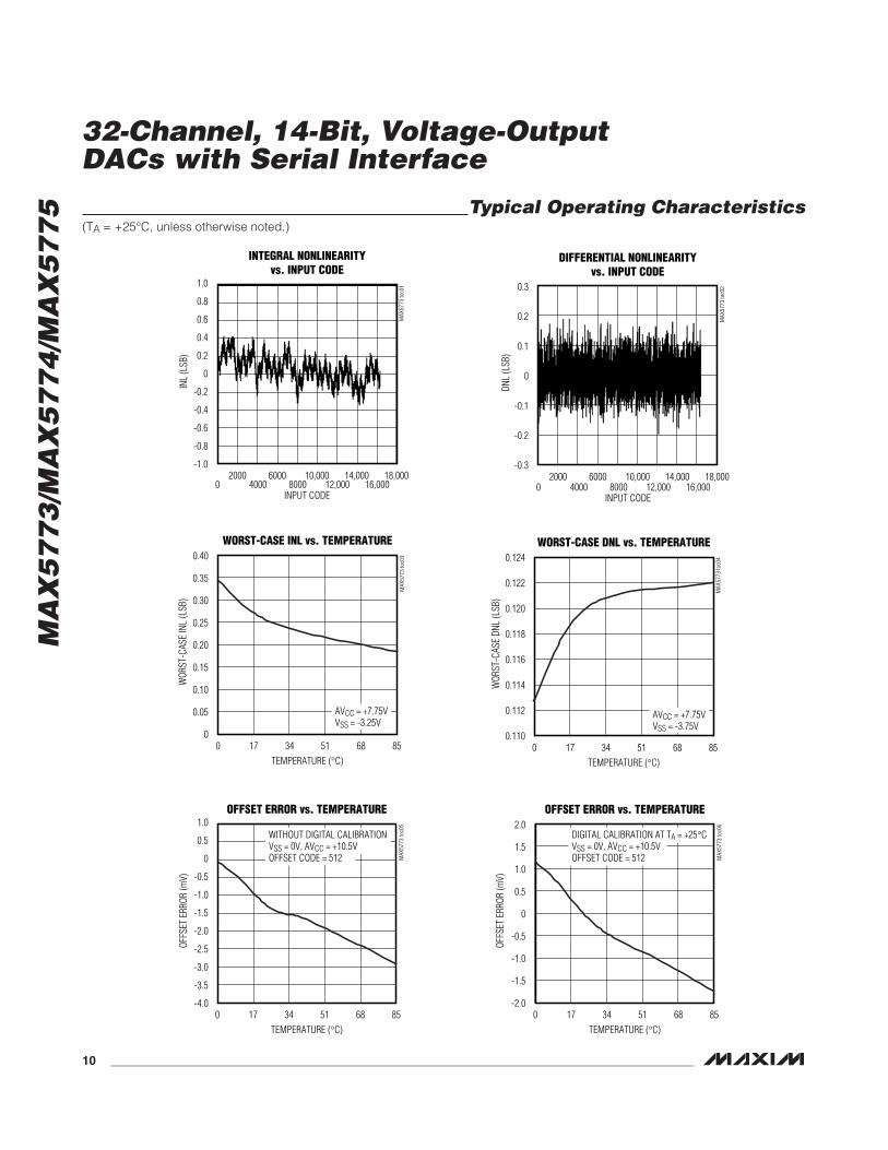
Typical Operating Characteristics(TA = +25°C, unless otherwise noted.)
MA
X5
77
3/M
AX
57
74
/MA
X5
77
5
32-Channel, 14-Bit, Voltage-OutputDACs with Serial Interface
______________________________________________________________________________________ 11
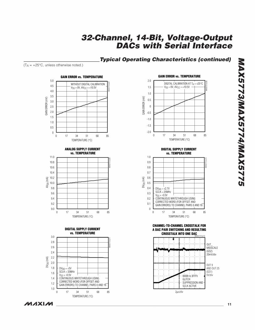
Typical Operating Characteristics (continued)(TA = +25°C, unless otherwise noted.)
0
1.5
1.0
0.5
2.0
2.5
3.0
3.5
4.0
4.5
5.0
0 3417 51 68 85
GAIN ERROR vs. TEMPERATURE
MAX
5773
toc0
7
TEMPERATURE (°C)
GAIN
ERR
OR (m
V)
WITHOUT DIGITAL CALIBRATIONVSS = 0V, AVCC = +10.5V
-2.0
-1.5
-1.0
-0.5
0
0.5
1.0
1.5
2.0
0 17 34 51 68 85
GAIN ERROR vs. TEMPERATURE
MAX
5773
toc0
8
TEMPERATURE (°C)GA
IN E
RROR
(mV)
DIGITAL CALIBRATION AT TA = +25°CVSS = 0V, AVCC = +10.5V
9.0
9.6
9.4
9.2
9.8
10.0
10.2
10.4
10.6
10.8
11.0
0 3417 51 68 85
ANALOG SUPPLY CURRENT vs. TEMPERATURE
MAX
5773
toc0
9
TEMPERATURE (°C)
AVDD
(mA)
0
0.3
0.2
0.1
0.4
0.5
0.6
0.7
0.8
0.9
1.0
0 3417 51 68 85
DIGITAL SUPPLY CURRENTvs. TEMPERATURE
MAX
5773
toc1
0
TEMPERATURE (°C)
DVDD
(mA)
DVDD = +2.7VSCLK = 25MHzVSS = -0.5VCONTINUOUS WRITETHROUGH USINGCORRECTED WORD (FOR OFFSET ANDGAIN ERRORS) TO CHANNEL PAIRS 0 AND 16
1.0
1.6
1.4
1.2
1.8
2.0
2.2
2.4
2.6
2.8
3.0
0 3417 51 68 85
DIGITAL SUPPLY CURRENTvs. TEMPERATURE
MAX
5773
toc1
1
TEMPERATURE (°C)
DVDD
(mA)
DVDD = +5VSCLK = 33MHzVSS = -0.5VCONTINUOUS WRITETHROUGH USINGCORRECTED WORD (FOR OFFSET ANDGAIN ERRORS) TO CHANNEL PAIRS 0 AND 16
CHANNEL-TO-CHANNEL CROSSTALK FORA DAC PAIR SWITCHING AND RESULTING
CROSSTALK INTO ONE DAC
OUT_MIDSCALE(GS2)20mV/div
MAX5773 toc12
2µs/div
0000h to 3FFFhGLITCHSUPPRESSION ANDSCLK ACTIVE
OUT 9AND OUT 25(GS1)5V/div

MA
X5
77
3/M
AX
57
74
/MA
X5
77
5
32-Channel, 14-Bit, Voltage-OutputDACs with Serial Interface
12 ______________________________________________________________________________________
400ns/div
DIGITAL FEEDTHROUGH(5V CLOCK)
OUT_10mV/div
SCLK5V/div
MAX5773 toc13
DVDD = +5V
2µs/div
LARGE-SIGNAL STEP RESPONSE(LOW TO HIGH)
OUT_5V/div
CS2V/div
MAX5773 toc14
2µs/div
LARGE-SIGNAL STEP RESPONSE(HIGH TO LOW)
OUT_5V/div
CS2V/div
MAX5773 toc15
Typical Operating Characteristics (continued)(TA = +25°C, unless otherwise noted.)
1µs/div
MAJOR CARRY TRANSITION1FFFh TO 2000h
WITH GLITCH SUPPRESSION
OUT_20mV/div
CS2V/div
MAX5773 toc17
1µs/div
MAJOR CARRY TRANSITION2000h TO 1FFFh
WITH GLITCH SUPPRESSION
OUT_20mV/div
CS2V/div
MAX5773 toc18
0.0001
10
0.001
1000
100
10,000
100,000
0 21 3 4 5
DVDD SUPPLY CURRENTvs. LOGIC INPUT VOLTAGE
MAX
5773
toc1
9
LOGIC INPUT VOLTAGE (V)
SUPP
LY C
URRE
NT (µ
A)
1
0.1
0.01 ALL LOGIC INPUTSCONNECTEDDVDD = +5V
0
10
5
20
15
25
30
0 3417 51 68 85
TOTAL SUPPLY SHUTDOWN CURRENTvs. TEMPERATURE
MAX
5773
toc2
0
TEMPERATURE (°C)
SHUT
DOW
N CU
RREN
T (µ
A)
AIDD + DIDD + AICC + ISS
AVCC = +7.75VVSS = -2.75V
NOISE VOLTAGE DENSITY
MAX
5773
toc1
6
FREQUENCY (kHz)1000100101
10
100
1000
10.1 10,000
NOIS
E (n
V/√H
z)

MA
X5
77
3/M
AX
57
74
/MA
X5
77
5
32-Channel, 14-Bit, Voltage-OutputDACs with Serial Interface
______________________________________________________________________________________ 13
MA
X5
77
3/M
AX
57
74
/MA
X5
77
5
Pin Description
PIN
68 TQFN 64 TQFPNAME FUNCTION
1, 16, 34, 35, 36,51, 52, 53, 68
15, 33, 34,49, 64
N.C. No Connection. Not internally connected.
2, 50, 59 1, 48, 55 AVCC Output-Amplifier Positive Supply Input. Bypass to AGND with a 0.1µF capacitor.
3 2 OUT9 DAC9 Buffered Analog Output Voltage
4 3 OUT8 DAC8 Buffered Analog Output Voltage
5 4 OUT7 DAC7 Buffered Analog Output Voltage
6 5 I.C. Internally Connected. Do not make any connections to I.C.
7 6 OUT6 DAC6 Buffered Analog Output Voltage
8 7 OUT5 DAC5 Buffered Analog Output Voltage
9 8 OUT4 DAC4 Buffered Analog Output Voltage
10, 46 9, 44 AGND Analog Ground
11 10 OUT3 DAC3 Buffered Analog Output Voltage
12, 33, 47 11, 32, 45 VSS Bypass to AGND with a 0.1µF capacitor
13 12 OUT2 DAC2 Buffered Analog Output Voltage
14 13 OUT1 DAC1 Buffered Analog Output Voltage
15 14 OUT0 DAC0 Buffered Analog Output Voltage
17, 25 16, 24 DVDD Digital Power-Supply Input. Bypass to DGND with a 0.1µF capacitor.
18, 26 17, 25 DGND Digital Ground
19 18 GS2Ground-Sense Analog Input 2. Offsets the DAC amplifier outputs OUT0, OUT1,OUT2, OUT16, OUT17, and OUT18 by ±0.5V to compensate for a remote systemground potential difference.
20 19 DSPDigital Serial-Interface Mode-Select Input. Drive low for DSP interface mode. Drivehigh for SPI interface mode.
21 20 CS Active-Low Digital Chip-Select Input
22 21 DOUTDigital Serial Data Output. Use DOUT to daisy chain or read the contents of theinternal registers. DOUT data clocks out on the falling edge of SCLK, MSB first.
23 22 SCLK Digital Serial Clock Input
24 23 DIN Digital Serial Data Input. Data clocks in on the falling edge of SCLK.
27 26 LDACActive-Low Digital Load DAC Input. Drive this asynchronous input low to transfer thecontents of the input register to their respective DAC registers and update all DACoutputs accordingly.
28 27 RESETActive-Low Reset Input. Drive this asynchronous input low to initiate a power-onreset. See the Power-On Reset section for further information.
29 28 GS1Ground-Sense Analog Input 1. Offsets the DAC amplifier outputs OUT3–OUT15 andOUT19–OUT31 by ±0.5V to compensate for a remote system ground potentialdifference.
30, 60 29, 56 REFGND Reference Ground

MA
X5
77
3/M
AX
57
74
/MA
X5
77
5
Detailed DescriptionThe MAX5773/MAX5774/MAX5775 are 32-channel, 14-bit, voltage-output DACs. All devices accept a +3.0Vexternal reference input at REF. An internal offset DACallows all outputs to be offset up to -5V (see Table 1).
A 33MHz SPI-/QSPI-/MICROWIRE- or DSP-compatibleserial interface (see Figure 1) controls theMAX5773/MAX5774/MAX5775. Use DSP to select theDSP mode or the SPI/QSPI/MICROWIRE mode.
Each DAC has a double-buffered input structure tominimize the digital-noise feedthrough from the digitalinputs to the outputs. The two buffers are organized as
an input register followed by a DAC register. Input reg-isters update the DAC registers independently or simul-taneously with a single software or hardware command.Each DAC channel has its own offset and gain registersthat calibrate offset and gain errors for a given channel.The MAX5773/MAX5774/MAX5775 are divided into twobanks of 16 channels to provide real-time calibration ofchannel pairs. Channel bank pairs are ordered as(bank 0:bank 1) OUT0:OUT16, OUT1:OUT17 …OUT14:OUT30, OUT15:OUT31.
An offset DAC allows all the outputs to be offset up to-5V and dual ground-sensing inputs (GS1 and GS2)allow the output voltages to be referenced to remote
32-Channel, 14-Bit, Voltage-OutputDACs with Serial Interface
14 ______________________________________________________________________________________
Pin Description
PIN
68 TQFN 64 TQFPNAME FUNCTION
31 30 REFAnalog Reference Voltage Input. Connect a +3V reference to REF and bypass toREFGND with a 0.1µF capacitor.
32, 61 31, 57 AVDD Analog Power-Supply Input. Bypass to AGND with a 0.1µF capacitor.
37 35 OUT16 DAC16 Buffered Analog Output Voltage
38 36 OUT17 DAC17 Buffered Analog Output Voltage
39 37 OUT18 DAC18 Buffered Analog Output Voltage
40 38 OUT19 DAC19 Buffered Analog Output Voltage
41 39 OUT20 DAC20 Buffered Analog Output Voltage
42 40 OUT21 DAC21 Buffered Analog Output Voltage
43 41 OUT22 DAC22 Buffered Analog Output Voltage
44 42 OUT23 DAC23 Buffered Analog Output Voltage
45 43 OUT24 DAC24 Buffered Analog Output Voltage
48 46 OUT25 DAC25 Buffered Analog Output Voltage
49 47 OUT26 DAC26 Buffered Analog Output Voltage
54 50 OUT27 DAC27 Buffered Analog Output Voltage
55 51 OUT28 DAC28 Buffered Analog Output Voltage
56 52 OUT29 DAC29 Buffered Analog Output Voltage
57 53 OUT30 DAC30 Buffered Analog Output Voltage
58 54 OUT31 DAC31 Buffered Analog Output Voltage
62 58 OUT15 DAC15 Buffered Analog Output Voltage
63 59 OUT14 DAC14 Buffered Analog Output Voltage
64 60 OUT13 DAC13 Buffered Analog Output Voltage
65 61 OUT12 DAC12 Buffered Analog Output Voltage
66 62 OUT11 DAC11 Buffered Analog Output Voltage
67 63 OUT10 DAC10 Buffered Analog Output Voltage
EP — EP Exposed Paddle. Connect to VSS.
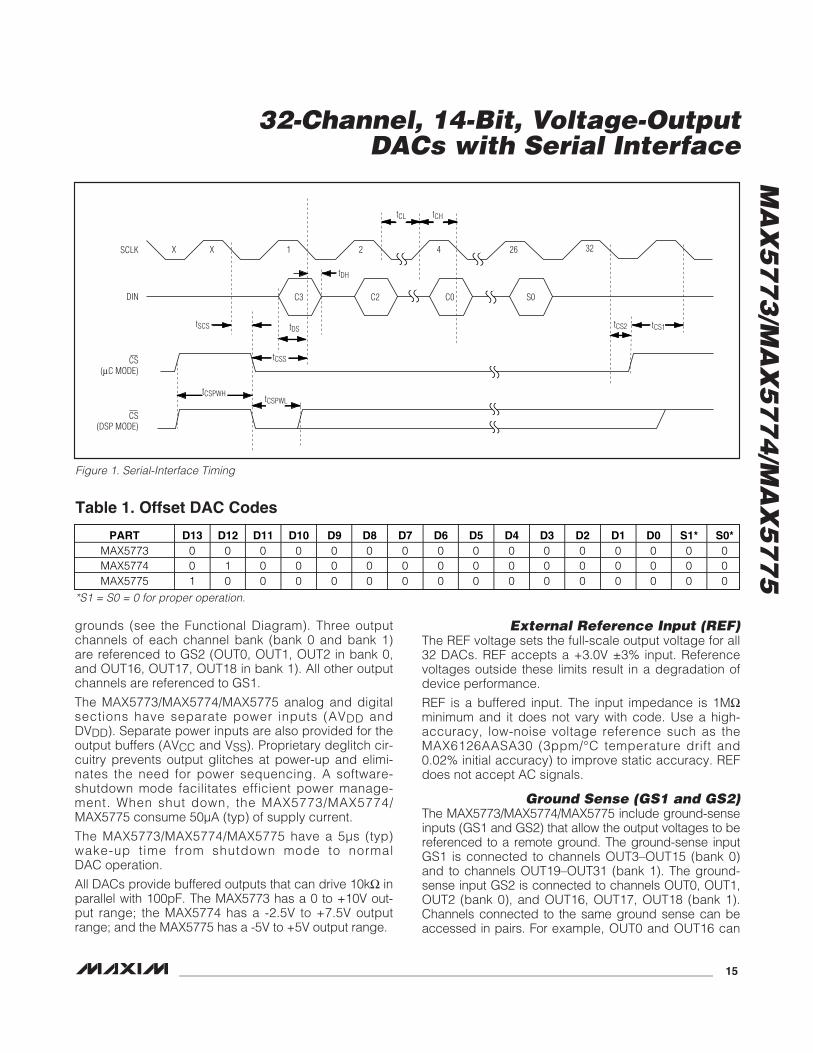
grounds (see the Functional Diagram). Three outputchannels of each channel bank (bank 0 and bank 1)are referenced to GS2 (OUT0, OUT1, OUT2 in bank 0,and OUT16, OUT17, OUT18 in bank 1). All other outputchannels are referenced to GS1.
The MAX5773/MAX5774/MAX5775 analog and digitalsections have separate power inputs (AVDD andDVDD). Separate power inputs are also provided for theoutput buffers (AVCC and VSS). Proprietary deglitch cir-cuitry prevents output glitches at power-up and elimi-nates the need for power sequencing. A software-shutdown mode facilitates efficient power manage-ment. When shut down, the MAX5773/MAX5774/MAX5775 consume 50µA (typ) of supply current.
The MAX5773/MAX5774/MAX5775 have a 5µs (typ)wake-up time from shutdown mode to normalDAC operation.
All DACs provide buffered outputs that can drive 10kΩ inparallel with 100pF. The MAX5773 has a 0 to +10V out-put range; the MAX5774 has a -2.5V to +7.5V outputrange; and the MAX5775 has a -5V to +5V output range.
External Reference Input (REF)The REF voltage sets the full-scale output voltage for all32 DACs. REF accepts a +3.0V ±3% input. Referencevoltages outside these limits result in a degradation ofdevice performance.
REF is a buffered input. The input impedance is 1MΩminimum and it does not vary with code. Use a high-accuracy, low-noise voltage reference such as theMAX6126AASA30 (3ppm/°C temperature drift and0.02% initial accuracy) to improve static accuracy. REFdoes not accept AC signals.
Ground Sense (GS1 and GS2)The MAX5773/MAX5774/MAX5775 include ground-senseinputs (GS1 and GS2) that allow the output voltages to bereferenced to a remote ground. The ground-sense inputGS1 is connected to channels OUT3–OUT15 (bank 0)and to channels OUT19–OUT31 (bank 1). The ground-sense input GS2 is connected to channels OUT0, OUT1,OUT2 (bank 0), and OUT16, OUT17, OUT18 (bank 1).Channels connected to the same ground sense can beaccessed in pairs. For example, OUT0 and OUT16 can
MA
X5
77
3/M
AX
57
74
/MA
X5
77
5
32-Channel, 14-Bit, Voltage-OutputDACs with Serial Interface
______________________________________________________________________________________ 15
SCLK X X 1 2 4 26
DIN S0C0C2C3
tCL tCH
tDH
tDS tCS2 tCS1
tCSS
tSCS
tCSPWLtCSPWH
CS(DSP MODE)
CS(µC MODE)
32
Figure 1. Serial-Interface Timing
PART D13 D12 D11 D10 D9 D8 D7 D6 D5 D4 D3 D2 D1 D0 S1* S0*MAX5773 0 0 0 0 0 0 0 0 0 0 0 0 0 0 0 0MAX5774 0 1 0 0 0 0 0 0 0 0 0 0 0 0 0 0MAX5775 1 0 0 0 0 0 0 0 0 0 0 0 0 0 0 0
Table 1. Offset DAC Codes
*S1 = S0 = 0 for proper operation.
MA
X5
77
3/M
AX
57
74
/MA
X5
77
5
be accessed as a pair (see Figure 3 for pairing of out-put channels).
The ground-sense input voltage range (VGS1 or VGS2)is -0.5V to +0.5V with respect to AGND. VGS is addedto the output voltage with unity gain. Ensure that theresulting output voltage is within the valid output volt-age range set by the power supplies. Refer to theOutput Amplifiers (OUT0–OUT31) section for the effectof the ground-sense inputs on the DAC outputs.
Offset DACThe MAX5773/MAX5774/MAX5775 feature an offsetDAC that determines the output voltage range. Whileeach device provides an allowable output voltagerange, the offset DAC determines the endpoint voltagesof the range. Table 1 shows the offset DAC code nec-essary for each device’s output-voltage range.
The MAX5773/MAX5774/MAX5775 offset DAC can beprogrammed with any of the three output voltage ranges.The specifications in the Electrical Characteristics tableare only guaranteed (production tested) for the offsetcode associated with each particular part number.
The offset DAC is summed with the GS_ input voltage(see the Functional Diagram). Any change in the offsetDAC affects all 32 DACs.
The offset DAC is also double buffered with an inputand DAC register.
Software commands for the MAC-bypass for all chan-nels and load-DAC for all channels do not affect the off-set DAC.
The data format for writing to the offset DAC is: controlbits C3–C0 = 0011, address bits A5–A0 = 110000, 14data bits (and S1, S0), and 6 don’t-care bits as shownin Table 2.
Output Amplifiers (OUT0–OUT31)All DAC outputs are internally buffered. The internalbuffers provide gain, improved load regulation, andglitch suppression for the DAC outputs. The outputbuffers slew at 1V/µs and can drive 10kΩ in parallelwith 100pF. The output buffers are powered by AVCCand VSS. AVCC and VSS determine the maximum outputvoltage range of the device.
The input code, the voltage reference, the offset DACoutput, the voltage on GS1 (or GS2), and the gain of theoutput amplifier determine the output voltage. CalculateVOUT as follows:
VGAIN V DAC CODE OFFSET DAC CODE
VOUTREF
GS=× × −
+( )
_214
32-Channel, 14-Bit, Voltage-OutputDACs with Serial Interface
16 ______________________________________________________________________________________
OUT_
±0.5 LSB
tS
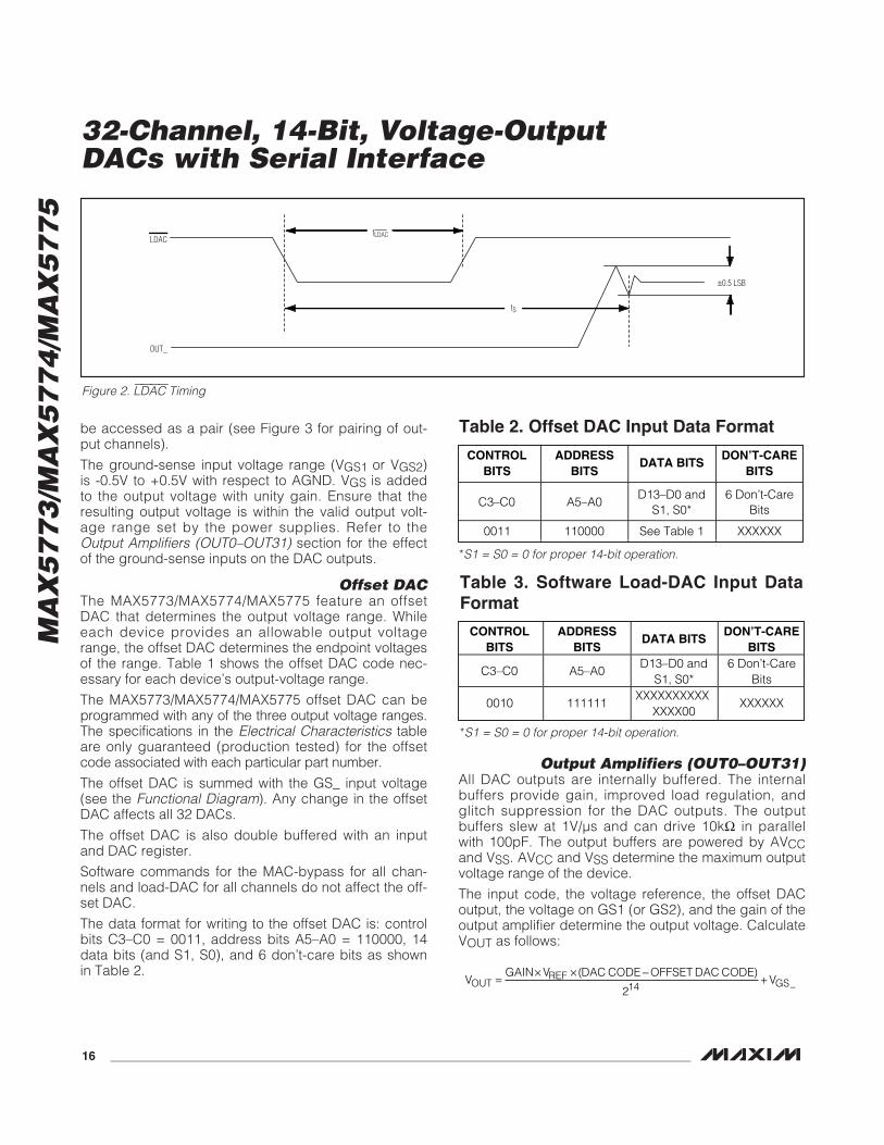
tLDACLDAC
Figure 2. LDAC Timing
CONTROLBITS
ADDRESSBITS
DATA BITSDON’T-CARE
BITS
C3–C0 A5–A0D13–D0 and
S1, S0*6 Don’t-Care
Bits
0011 110000 See Table 1 XXXXXX
Table 2. Offset DAC Input Data Format
*S1 = S0 = 0 for proper 14-bit operation.
CONTROLBITS
ADDRESSBITS
DATA BITSDON’T-CARE
BITS
C3–C0 A5–A0D13–D0 and
S1, S0*6 Don’t-Care
Bits
0010 111111XXXXXXXXXX
XXXX00XXXXXX
Table 3. Software Load-DAC Input DataFormat
*S1 = S0 = 0 for proper 14-bit operation.

MA
X5
77
3/M
AX
57
74
/MA
X5
77
5
32-Channel, 14-Bit, Voltage-OutputDACs with Serial Interface
______________________________________________________________________________________ 17
CHANNEL-BANK SELECTION
ADDRESS BITS
A5 A4CHANNEL BANK(S) SELECTED
0 0 CHANNEL BANK 00 1 CHANNEL BANK 11 0 BOTH CHANNEL BANKS1 1 OFFSET CHANNEL AND ALL CHANNEL OPERATION
INPUT REGISTER, DAC REGISTER, GAIN REGISTER, AND OFFSET REGISTER ACCESS*
BANK 0 BANK 1 BANK 0 AND BANK 1 ADDRESS BITS
A5 A4 A5 A4 A5 A4
0 0 0 1 1 0A3 A2 A1 A0
CHANNEL 0 CHANNEL 16 CHANNEL 0 AND CHANNEL 16 0 0 0 0
CHANNEL 1 CHANNEL 17 CHANNEL 1 AND CHANNEL 17 0 0 0 1
CHANNEL 2 CHANNEL 18 CHANNEL 2 AND CHANNEL 18 0 0 1 0
CHANNEL 3 CHANNEL 19 CHANNEL 3 AND CHANNEL 19 0 0 1 1
CHANNEL 4 CHANNEL 20 CHANNEL 4 AND CHANNEL 20 0 1 0 0
CHANNEL 5 CHANNEL 21 CHANNEL 5 AND CHANNEL 21 0 1 0 1
CHANNEL 6 CHANNEL 22 CHANNEL 6 AND CHANNEL 22 0 1 1 0
CHANNEL 7 CHANNEL 23 CHANNEL 7 AND CHANNEL 23 0 1 1 1
CHANNEL 8 CHANNEL 24 CHANNEL 8 AND CHANNEL 24 1 0 0 0
CHANNEL 9 CHANNEL 25 CHANNEL 9 AND CHANNEL 25 1 0 0 1
CHANNEL 10 CHANNEL 26 CHANNEL 10 AND CHANNEL 26 1 0 1 0
CHANNEL 11 CHANNEL 27 CHANNEL 11 AND CHANNEL 27 1 0 1 1
CHANNEL 12 CHANNEL 28 CHANNEL 12 AND CHANNEL 28 1 1 0 0
CHANNEL 13 CHANNEL 29 CHANNEL 13 AND CHANNEL 29 1 1 0 1
CHANNEL 14 CHANNEL 30 CHANNEL 14 AND CHANNEL 30 1 1 1 0
CHANNEL 15 CHANNEL 31 CHANNEL 15 AND CHANNEL 31 1 1 1 1
* C HA NN EL PA IR AC CE SS (B AN K 0 A ND BA NK 1) O NL Y P ER M IT TE D F OR W R IT ET HR O UG H, MA C-BY P AS S,A ND L OA D -D AC CO MM AN D S.
ACCESSING OFFSET CHANNEL AND ALL CHANNELS (ADDRESS BITS A5 AND A4 = 11)
ACCESSING CONFIGURATION REGISTER (CONTROL BITS C3–C0 = 1100 OR 1101, ADDRESSBITS A5 AND A4 = 00)
ADDRESS BITSA3 A2 A1 A0
REGISTER SELECTED
0 0 0 0 CONFIGURATION REGISTER (SEE TABLE 8)0001 THROUGH 1111 UNUSED
ADDRESS BITSA3 A2 A1 A0
REGISTER SELECTED
0 0 0 0 OFFSET CHANNEL0001 THROUGH 1110 UNUSED
1 1 1 1ALL CHANNELS (SOFTWARE LOAD-DAC AND MAC-BYPASS
COMMANDS ONLY)
Figure 3. Address Space When Accessing DAC Channel Register(s), Offset Register(s), Gain Register(s), and Special Registers

MA
X5
77
3/M
AX
57
74
/MA
X5
77
5 GAIN = 10/3 for the MAX5773/MAX5774/MAX5775.
Load-DAC (LDAC) InputThe MAX5773/MAX5774/MAX5775 feature an active-low LDAC input that allows the outputs (OUT_) toupdate asynchronously. Keep LDAC high during nor-mal operation (when the device is controlled onlythrough the serial interface). Drive LDAC low to simulta-neously update all DAC outputs with data from theirrespective input registers. Figure 2 shows the LDACtiming with respect to OUT_.
A software command can also perform the LDAC oper-ation. To initiate LDAC by software, set control bitsC3–C0 = 0010, address bits A5–A0 = 111111, and alldata bits to don’t care. See Table 3 for the data format.This operation updates all DAC outputs simultaneously.The software load-DAC command for all channels doesnot affect the offset DAC.
Software MAC-BypassThe MAX5773/MAX5774/MAX5775 feature a softwareMAC-bypass command that loads data into the DACdirectly from DIN. Software MAC-bypass loads one DAC,a pair of DACs, or all 32 DACs with a data word (D13–D0and S1, S0) entered at DIN and the selected DAC out-put(s) are simultaneously updated. Software MAC-bypass bypasses gain and offset calibration, sendingthe input data directly to the DAC register immediatelyupdating the selected DAC outputs. After executingMAC-bypass on a channel(s), previously calibrated datacan be reloaded into the DAC by executing softwareload-DAC or hardware LDAC (see Figure 4). Using soft-ware MAC-bypass, the DAC output(s) can be set to theground-sense value or any arbitrary value within the DACoutput voltage range.
To activate software MAC-bypass, set control bitsC3–C0 = 0111. The address bits (A5–A0) select theDAC(s) to be updated and the data bits (D13–D0) con-trol the DAC output voltage value. Table 4 shows theinput data format for the software-controlled MAC-bypass command.
Reset (RESET)The MAX5773/MAX5774/MAX5775 feature an active-low RESET logic input that asynchronously sets all theregisters to code 0000h (power-up state). The serialinterface can also issue a software-reset command.Setting the control bits C3–C0 = 1111 performs thesame function as driving the logic input RESET low.Table 5 shows the reset data format for the software-controlled reset command. The software reset does notwork in daisy-chain mode. Reprogram the offset DACafter asserting a software or hardware reset.
Serial InterfaceThe MAX5773/MAX5774/MAX5775 allow channel updateseither individually or in pairs. This is achieved by dividingthe 32 channels into two channel banks, with 16 channelsin each bank. Channel bank 0 contains output channelsOUT0–OUT15 and channel bank 1 contains channelsOUT16–OUT31. A channel from bank 0 is paired with achannel from bank 1 and is ordered as OUT0:OUT16,OUT1:OUT17...OUT14:OUT30, OUT15:OUT31.
A 3-wire SPI-/QSPI-/MICROWIRE- and DSP-compatibleserial interface controls the MAX5773/MAX5774/MAX5775. The interface requires a
32-Channel, 14-Bit, Voltage-OutputDACs with Serial Interface
18 ______________________________________________________________________________________
CONTROLBITS
ADDRESSBITS
DATA BITSDON’T-CARE
BITS
C3–C0 A5–A0D13–D0 and
S1, S0*6 Don’t-Care
Bits
1111 XXXXXXXXXXXXXXXX
XXXX00XXXXXX
Table 5. Reset Data Format
*S1 = S0 = 0 for proper 14-bit operation.
CONTROLBITS
ADDRESSBITS
DATA BITSDON’T-CARE
BITS
C3–C0 A5–A0D13–D0 and
S1, S0*6 Don’t-Care
Bits
0111 See Figure 3D13–D0,S1, S0*
XXXXXX
Table 4. MAC-Bypass Data Format
*S1 = S0 = 0 for proper 14-bit operation.
CONTROLBITS
ADDRESSBITS
DATA BITS6 DON’T-
CARE BITS
MSB LSB
C3–C0 A5–A0D13–D0 and
S1, S0*XXXXXX
Table 6. Serial Data Format
*S1 = S0 = 0 for proper 14-bit operation.
INPUT_REGISTER
GAIN
OFFSET
DAC_REGISTER
CALIBRATEDDATA REGISTER
DAC_
LDAC
+*
MAC-BYPASSDIN
Figure 4. MAC-Bypass Functional Diagram

32-bit command word to control the device. The com-mand word consists of 4 control bits, 6 address bits, 14data bits (and S1, S0 = 00), and 6 don’t-care bits. Table6 shows the general serial data format. The control bitscontrol various write and read commands, as well as theload DAC and MAC-bypass commands. Table 8 showsthe control-bit functions. The address bits select the reg-ister(s) to update. Figure 3 shows the address functions.The data bits control the voltage value of the DAC out-puts. DIN data is clocked in at the falling edge of SCLK(Figure 1).
MA
X5
77
3/M
AX
57
74
/MA
X5
77
5
32-Channel, 14-Bit, Voltage-OutputDACs with Serial Interface
______________________________________________________________________________________ 19
R E G I ST ER C O N T R O L
B IT S( C 3 – C 0 )
ADDRESSBITS
(A5–A0)
D A T A B I T S( D 1 3 – D 0 A N D S1 , S0 * )
6DON’T-CAREBITS
OffsetRegister
1001 S ee Fi g ur e 3S ee Tab l e
10X X X X X X
GainRegister
1000 S ee Fi g ur e 3 S ee Tab l e 9 X X X X X X
Table 7. Gain and Offset Register InputData Format
*S1 = S0 = 0 for proper 14-bit operation.
4 CONTROL BITS
C3 C2 C1 C0CONTROL-BIT DESCRIPTION
0 0 0 0No operation (NOP). No internal registers change state. The NOP command can be passed toDOUT depending on the state of the configuration register. Address bits A5–A0 and data bitsD13–D0 are ignored.
0 0 0 1This instruction writes and calibrates the 14-bit input data word for gain and offset errors. DriveLDAC low or use a software load-DAC command to update the selected DAC outputs.
0 0 1 0Software load-DAC command. Updates the output of the selected DAC channel(s). Depending onthe address bits, this command updates one DAC output, a pair of DAC outputs, or all the DACoutputs simultaneously. Data bits D13–D0 are ignored.
0 0 1 1This instruction writes and calibrates the 14-bit input data word for gain and offset errors andimmediately updates the DAC outputs for the selected address.
0 1 0 0Read command. Depending on the address bits, one of the input register values is read backthrough DOUT. Data bits D13–D0 are ignored. See the Daisy-Chain Operation section.
0 1 0 1 Reserved; do not use.
0 1 1 0 Reserved; do not use.
0 1 1 1MAC-bypass command. Depending on the address bits, one, two, or all DAC registers are loadedwith a 14-bit data word at DIN. The input data is not calibrated for gain and offset errors (see theMAC-Bypass section). Selected DAC output(s) are immediately updated.
1 0 0 0Loads D13–D0 into one or two of the gain register(s) for the selected address. The data for theselected address is calibrated for gain error. Drive LDAC low or use a software load-DACcommand to update the selected DAC outputs.
1 0 0 1Loads D13–D0 into one or two of the offset register(s) for the selected address. The data for theselected address is calibrated for offset error. Drive LDAC low or use a software load-DACcommand to update the selected DAC outputs.
1 0 1 0 Read command. Reads one of the gain registers and presents the data at DOUT.
1 0 1 1 Read command. Reads one of the offset registers and presents the data at DOUT.
1 1 0 0 Write command. Loads D13–D0 into the configuration register.
1 1 0 1 Read command. Reads the contents of the configuration register.
1 1 1 0 Read command. Reads the DAC register for the selected address.
1 1 1 1 Reset instruction.
Table 8. Control-Bit Functions

MA
X5
77
3/M
AX
57
74
/MA
X5
77
5
Gain and Offset RegistersThe MAX5773/MAX5774/MAX5775 contain a gain andoffset register associated with each channel to correctreal-time gain and offset errors associated with eachchannel. The gain and offset registers can beaccessed individually or in pairs.
The gain word range is limited between 0 and 1. Thegain word is an unsigned 14-bit data word. A gain wordof 0000h is a special mapping to provide a gain ofabsolute one, i.e., no gain correction. For all the othergain word codes, the amount of gain correction variesproportionally to the gain word’s decimal value. Forexample, a gain word of 0001h is equivalent to a gainof 0.514 and a gain of 3FFFh is equivalent to 1 - 0.514
(see Table 9). To access the gain register, set controlbits C3–C0 = 1000 (see Tables 7 and 8).
The offset has a range from -FS/2 to + (FS/2 - 1 LSB).The offset word is a 14-bit data word represented intwo’s complement. For example, an offset word equiva-lent to 1FFFh would provide an offset of FS/2 - 1 LSBand offset word of 2000h would provide an offset of-FS/2 (see Table 10). To access the offset register, setcontrol bits C3–C0 = 1001 (see Tables 7 and 8).
Configuration RegisterThe configuration register controls the advanced fea-tures of the MAX5773/MAX5774/MAX5775. Write to theconfiguration register by setting control bits C3–C0 =1100 and address bits 000000. Table 11 shows theconfiguration register data format for the D13–D0 databits. Table 12 shows the commands controlled by theconfiguration register.
DSP Mode (DSP)The MAX5773/MAX5774/MAX5775 provide a hardware-selectable DSP-interface mode. The active-low DSPlogic input selects the microcontroller (µC)-interface orDSP-interface mode. Drive DSP high for µC-interfacemode. Drive DSP low for DSP-interface mode. DSPmode, when active, allows chip select (CS) to go highbefore the entire 32-bit command word is clocked in.Figure 1 illustrates serial timing for both µC- and DSP-interface modes.
SINGWhen SING = 0, the MAX5773/MAX5774/MAX5775 arein daisy-chain mode. For daisy-chain operation, setDSP high (µC mode) and SING = 0.
32-Channel, 14-Bit, Voltage-OutputDACs with Serial Interface
20 ______________________________________________________________________________________
CONTROLLERDEVICE
DIN(0)
DOUT(0)
1
SCLKCS
DSP
MAX577_
DIN(1)
DOUT(1)SCLKCS
DSP
MAX577_
DIN(2)
DOUT(2)SCLKCS
DSP
MAX577_
Figure 5. Daisy-Chain Configuration
CODE (DATA BITS D13–D0) GAIN VALUE
0000h Unity Gain
0001h 0.000061
0002h 0.00012
: :
1FFFh 0.499938
2000h 0.5
: :
3FFEh 0.999877
3FFFh 0.999938
Table 9. Gain Register Code Values
CODE (DATA BITS D13–D0) OFFSET VALUE*
1FFFh FS/2 - 1 LSB
: :
0001h +1 LSB
0000h 0
3FFFh -1 LSB
: :
2000h -FS/2
Table 10. Offset Register Code Values
*1 LSB = FS/214
In daisy-chain operation, DOUT follows DIN after 32 clockcycles for a write command. For a read command, DOUTprovides only the 14 data bits (and S1, S0) in the nextcycle following the CS falling edge. Data is provided MSBfirst at DOUT on the falling edge of SCLK.
When SING = 1, the device is in stand-alone mode. Toreduce the time it takes to read data out, the read datais provided MSB first at DOUT on the last 16 cycles ofthe current command word. The device acts on an
incoming command word independent of the risingedge of CS. SING functionality is ignored in DSP mode.
Daisy-Chain OperationDaisy chain any number of the MAX5773/MAX5774/MAX5775 devices by connecting the DOUT of onedevice to DIN of another. Set DSP high and SING = 0for all devices in the daisy chain (see Figure 5).
MA
X5
77
3/M
AX
57
74
/MA
X5
77
5
32-Channel, 14-Bit, Voltage-OutputDACs with Serial Interface
______________________________________________________________________________________ 21
14 DATA BITSD13 D12 D11 D10 D9 D8 D7 D6 D5 D4 D3 D2 D1 D0 S1 S0
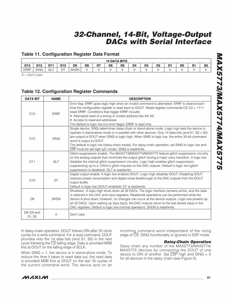
ERRF SING GLT DT SHDN X X X X X X X X X X X
Table 11. Configuration Register Data Format
X = Don’t care.
DATA BIT NAME DESCRIPTION
D13 ERRF
Error flag. ERRF goes logic high when an invalid command is attempted. ERRF is cleared eachtime the configuration register is read back to DOUT. Reset-register commands C3–C0 = 1111reset ERRF. Conditions that trigger ERRF include:• Attempted read of a wrong or invalid address bits A5–A0• Access to reserved addressesThe default is logic low (no error flags); ERRF is read only.
D12 SING
Single device. SING determines daisy-chain or stand-alone mode. Logic high sets the device tooperate in stand-alone mode or in parallel with other devices. Only 14 data bits (and S1, S0 = 00)are output to DOUT when SING is logic high. When SING is logic low, the entire 32-bit commandword is output to DOUT.The default is logic low (daisy-chain mode). For daisy-chain operation, set SING to logic low andDSP must be set high (µC mode). SING is read/write.
D11 GLT
Glitch-suppression enable. The MAX5773/MAX5774/MAX5775 feature glitch-suppression circuitryon the analog outputs that minimizes the output glitch during a major carry transition. A logic lowdisables the internal glitch-suppression circuitry. Logic high enables glitch suppression,suppressing up to a 120nV-s glitch impulse on the DAC outputs. Default is logic low (glitchsuppression is disabled). GLT is read/write.
D10 DT
Digital output enable. A logic low enables DOUT. Logic high disables DOUT. Disabling DOUTreduces power consumption and digital noise feedthrough to the DAC outputs from the DOUToutput buffer.Default is logic-low (DOUT enabled); DT is read/write.
D9 SHDN
Shutdown. A logic high shuts down all 32 DACs. The logic interface remains active, and the datais retained in the DAC and input registers. Read/write operations can be performed while thedevice is shut down; however, no changes can occur at the device outputs. Logic-low powers upall 32 DACs. Upon waking up (5µs (typ)), the DAC outputs return to the last stored value in theDAC registers. Default is logic low (normal operation). SHDN is read/write.
D8–D0 andS1, S0
X Don’t care.
Table 12. Configuration Register Commands

MA
X5
77
3/M
AX
57
74
/MA
X5
77
5
32-Channel, 14-Bit, Voltage-OutputDACs with Serial Interface
22 ______________________________________________________________________________________
W WD2 W WD1 W WD0 R XX R XX R XX X XX X XX X XXDIN(0)
CS
DOUT(0) WD1WWD2W XXRXXRWD0W RD0 X
X
X
X XX X XX
DOUT(1) W WD2 W WD1 W WD0 R XX RD1 RD0 XX
X X
XX
DOUT(2) W WD2 W WD1 W WD0 RD2 RD1 RD0
Figure 6. Example 1 of a Daisy-Chain Data Sequence
W/WD0 = 32-bit word with a write command; WD0 writes data for device 0. The 0 refers to the position in the daisy chain (0 is closestto the bus master). Devices 1 and 2 are devices further down the chain.RDn/X = 32-bit word with a 14-bit read output from from device “n” followed by don’t-care bits.X = Don’t care (for X in the data or command position).
W WD2 R XX W WD0 R XX W WD1 R XX X XX X XX X XXDIN(0)
CS
DOUT(0) XXRWD2W WD1WXXRWD0W RD0 XX XX X XX
DOUT(1) W WD2 RD1 W WD0 R XX W WD1 RD0 XX
XX
X
X
XX
DOUT(2) W WD2 RD1 W WD0 RD2 W WD1 RD0
Figure 7. Example 2 of a Daisy-Chain Data Sequence
W/WD0 = 32-bit word with a write command; WD0 writes data for device 0. The 0 refers to the position in the daisy chain (0 is closestto the bus master). Devices 1 and 2 are devices further down the chain.RDn/X = 32-bit word with a 14-bit read output from from device “n” followed by don’t-care bits.X = Don’t care (for X in the data or command position).

The MAX5773/MAX5774/MAX5775 support daisy-chainconnections of multiple devices. The default (power-up)configuration for the MAX5773/MAX5774/MAX5775assumes that the device may be part of a daisy chainof devices (SING = 0 and DSP = 1). For a write com-mand, DOUT follows DIN after 32 clock cycles in thedefault configuration. Figures 6 and 7 show examplesof daisy-chain data sequences.
Data ReadbackRead the contents of the MAX5773/MAX5774/MAX5775DAC and configuration registers at DOUT by issuing aread-data command. Control bits C3–C0 configure thedevice for the read-data modes (see Table 8). Theaddress bits select the register(s) to be read. The con-tents of the register(s) are clocked out MSB first atDOUT on the falling edge of SCLK. The output data for-mat depends on the status of DSP and SING. Table 13shows the manner in which data is written to DOUT.
Shutdown ModeThe MAX5773/MAX5774/MAX5775 feature a software-controlled, low-power shutdown mode.
Setting bit 9 of the configuration register to a logic high,disables the analog section of the device, forcing theoutputs to go high impedance. In shutdown, supplycurrent is reduced to 50µA typical. Data stored in theDAC and input registers is retained, and the deviceoutputs return to their previous values upon exitingshutdown. Wake-up time is 5µs (typ). The serial inter-face remains active while the device is in shutdown.
Power-Up StateThe MAX5773/MAX5774/MAX5775 monitor the fourpower supplies and maintain the output buffers in aknown state until sufficient voltage is available to ensurethat no output glitches occur. Once the minimum voltagethreshold has been exceeded, the device outputs comeup in the clear state (all outputs = 0).
Applications InformationAutomatic Test Equipment (ATE)
ApplicationsThe MAX5773/MAX5774/MAX5775 include many fea-tures suited for ATE applications. These devices arethe most highly integrated level-setting solution avail-able for high-density pin electronics boards, and pro-vide the output voltage ranges required by most ATEapplications. The offset DAC simultaneously adjusts thevoltage range of all 32 DACs, allowing optimization tothe application. The remote-sense feature (GS1 and
GS2) allows the pin electronic voltages to be refer-enced to the ground potential at the DUT site. An inte-grated offset and gain feature eliminates the need forcostly external circuitry.
The pipelined register architecture allows all 32 DACsto be updated simultaneously. This is valuable duringtest setups, as all values in the tester can be set andthen updated in unison with a single command.Accessing the serial interface or the LDAC inputupdates all 32 DACs simultaneously.
The low output noise of the MAX5773/MAX5774/MAX5775 allows direct connection to the pin electron-ics, eliminating the cost and PC board area of exter-nal filtering.
Modern pin electronics integrated circuits (PEICs) aretypically fabricated on high-speed processes with lowbreakdown voltages. Some devices require externalprotection on their reference inputs to satisfy absolutemaximum ratings. The MAX5773/MAX5774/MAX5775feature outputs that are almost rail-to-rail allowing theAVCC and VSS supplies to be set to voltages within theabsolute maximum ratings of the PEIC to guaranteethat the PEIC is protected in all situations.
Power Supplies, Bypassing,Decoupling, and Layout
Grounding and power-supply decoupling strongly influ-ence device performance. Digital signals can couplethrough the reference input, power supplies, and groundconnection. Proper grounding and layout can reducedigital feedthrough and crosstalk. For noisy environ-ments, bypass all power supplies with a 0.1µF and 1µFon each pin, as close to the device as possible.
The MAX5773/MAX5774/MAX5775 have four separatepower supplies. AVDD powers the internal analog cir-cuitry (except for the output buffers), and DVDD powersthe digital section of the device. AVCC and VSS powerthe output buffers.
MA
X5
77
3/M
AX
57
74
/MA
X5
77
5
32-Channel, 14-Bit, Voltage-OutputDACs with Serial Interface
______________________________________________________________________________________ 23

MA
X5
77
3/M
AX
57
74
/MA
X5
77
5
32-Channel, 14-Bit, Voltage-OutputDACs with Serial Interface
24 ______________________________________________________________________________________
DSP SING CONFIGURATION READ DATA AT DOUT
0 XStand-aloneDSP mode
DOUT provides the 14 data bits only (and S1, S0).The 14 d ata b i ts ( and S 1, S 0) ar e cl ocked out M S B fi r st at D O U T, on the l ast16 cl ock ed g es of the cur r ent r ead com m and w or d . S ee Fi g ur es 8, 9, and 10.
1 0Standard daisy-chain
configurationµC mode
For write commands, DOUT follows DIN after 32 clocks. The entire 32-bitwrite command word (both command word and data) is clocked out MSBfirst at DOUT. For read commands, the 14 data bits (and S1, S0) of theselected register are valid at DOUT starting with the first clock falling edgeafter the falling edge of CS (see Fi g ur es 6 and 7) .
1 1Stand-alone
µC mode
DOUT provides the 14 data bits (and S1, S0) of the selected register fromthe current read command word. The 14 data bits (and S1, S0) are clockedout MSB first at DOUT on the last 16 clock edges of the current readcommand word (see Figures 8, 9 and 10).
Table 13. Read-Data Modes with SING and DSP Controls
CONTROLLERDEVICE
DIN
DOUT
1 OR 0
SCLKCS
MAX577_
DSP
Figure 8. Stand-Alone Configuration
CONTROLLERDEVICE
DIN
DOUT
1 OR 0
1 OR 0
1 OR 0
SCLKCS
MAX577_
DIN
DOUTSCLKCS
MAX577_
DIN
DOUTSCLKCS
MAX577_
DSP
DSP
DSP
Figure 9. Example of a Parallel Configuration with Readback
Chip InformationPROCESS: BiCMOS

MA
X5
77
3/M
AX
57
74
/MA
X5
77
5
32-Channel, 14-Bit, Voltage-OutputDACs with Serial Interface
______________________________________________________________________________________ 25
C2C3 C1 C0 A5 A4 A3 A2 A1 A0 Sp Sp Sp Sp Sp Sp D13 D12 D11 D9 D8 D7 D6 D5 D4 D3 D2 D1 D0 S1* S0*
D13 D12 D11 D10 D9 D8 D7 D6 D5 D4 D3 D2 D1 D0 S1 S0
DIN(0)
SCLK
CS (µC)
CS (DSP)
DOUT(0)
OR
D10
1 8 17 24 32
SING = 1 (µC MODE) OR X (DSP MODE)††X = DON'T CARE.*S1 = S0 = 0 FOR PROPER 14-BIT OPERATION
Figure 10. Read Data Timing When Not Daisy Chained
58
59
60
61
62
54
55
56
57
63
38394041424344454647
TOP VIEW
52
53
35363748
64
65
66
67
68
23
22
21
20
19
27
26
25
24
18
29
28
32
31
30
34
33
495051
111098765432 16151413121 17
MAX5773MAX5774MAX5775
OUT10
OUT11
OUT12
OUT13
OUT14
OUT15
AVDD
REFGND
AVCC
OUT31
OUT30
OUT29
OUT28
OUT27
N.C.
N.C.
N.C.
OUT2
6
OUT2
5
V SS
AGND
OUT2
4
OUT2
3
OUT2
2
OUT2
1
OUT2
0
OUT1
9
OUT1
8
OUT1
7
OUT1
6
N.C.
N.C.
AVCC
N.C.
V SS
OUT3
AGND
OUT4
OUT5
OUT6
DVDD
N.C.
OUT0
OUT1
OUT2I.C
.
OUT7
OUT8
OUT9
AVCCN.C.
DSP
TQFN
GS2
DOUT
CS
DIN
SCLK
DGNDDVDD
RESET
LDAC
REFGND
GS1
AVDD
REF
VSS
DGND
N.C.
EP
Pin Configurations (continued)

MA
X5
77
3/M
AX
57
74
/MA
X5
77
5
32-Channel, 14-Bit, Voltage-OutputDACs with Serial Interface
26 ______________________________________________________________________________________
INPUTREGISTER
0
GAIN
OFFSET
DAC0REGISTER
DAC0+*
AVCC
VSS
INPUTREGISTER
1
GAIN
OFFSET
DAC1REGISTER
DAC1+*
AVCC
VSS
INPUTREGISTER
2
GAIN
OFFSET
DAC2REGISTER
DAC2+*
AVCC
VSS
INPUTREGISTER
30
GAIN
OFFSET
DAC30REGISTER
DAC30+*
AVCC
VSS
INPUTREGISTER
31
GAIN
OFFSET
DAC31REGISTER
DAC31+*
AVCC
VSS
GAIN
OFFSET
OFFSETDAC REGISTER
OFFSETDAC
+*OFFSET DAC
INPUTREGISTER
REF BUFFER
DIGITAL CONTROL LOGIC
AVCC
VSS
AGND
DGND
REFGND
AVDD
DVDD
POWERMANAGEMENT
OUT31
OUT30
OUT2
OUT1
OUT0
GS1GS2REFCS SCLK DIN DSP LDAC RESET DOUT
3 OF
6 C
HANN
ELS
ON G
S2
MAX5773MAX5774MAX5775
ETC.
Functional Diagram

MA
X5
77
3/M
AX
57
74
/MA
X5
77
5
32-Channel, 14-Bit, Voltage-OutputDACs with Serial Interface
______________________________________________________________________________________ 27
Package Information(The package drawing(s) in this data sheet may not reflect the most current specifications. For the latest package outline information,go to www.maxim-ic.com/packages.)
68L
QFN
TH
IN.E
PS
PACKAGE OUTLINE
21-0142 21
E
68L THIN QFN, 10x10x0.8mm

32-Channel, 14-Bit, Voltage-OutputDACs with Serial Interface
Maxim cannot assume responsibility for use of any circuitry other than circuitry entirely embodied in a Maxim product. No circuit patent licenses areimplied. Maxim reserves the right to change the circuitry and specifications without notice at any time.
28 ____________________Maxim Integrated Products, 120 San Gabriel Drive, Sunnyvale, CA 94086 408-737-7600
© 2006 Maxim Integrated Products Printed USA is a registered trademark of Maxim Integrated Products, Inc.
MA
X5
77
3/M
AX
57
74
/MA
X5
77
5M
AX
57
73
/MA
X5
77
4/M
AX
57
75
MA
X5
77
3/M
AX
57
74
/MA
X5
77
5
Package Information (continued)(The package drawing(s) in this data sheet may not reflect the most current specifications. For the latest package outline information,go to www.maxim-ic.com/packages.)
PACKAGE OUTLINE
21-0142 22
E
68L THIN QFN, 10x10x0.8mm