Embed Size (px)
Citation preview
OPA363, OPA2363OPA364, OPA2364, OPA4364
www.ti.com SBOS259C –SEPTEMBER 2002–REVISED MAY 2013
1.8V, 7MHz, 90dB CMRR,Single-Supply, Rail-to-Rail I/O
Operational AmplifierCheck for Samples: OPA363, OPA2363, OPA364, OPA2364, OPA4364
1FEATURES DESCRIPTIONThe OPA363 and OPA364 families are high-
2• 1.8V Operationperformance CMOS operational amplifiers optimized
• MicroSize Packages for very low voltage, single-supply operation. These• Bandwidth: 7MHz miniature, low-cost amplifiers are designed to operate
on single supplies from 1.8V (±0.9V) to 5.5V• CMRR: 90dB (typical)(±2.75V). Applications include sensor amplification• Slew Rate: 5V/μs and signal conditioning in battery-powered systems.
• Low Offset: 500μV (max)The OPA363 and OPA364 families offer excellent
• Quiescent Current: 750μA/Channel (max) CMRR without the crossover associated with• Shutdown Mode: < 1µA/Channel traditional complimentary input stages. This results in
excellent performance for driving Analog-to-Digital(A/D) converters without degradation of differentialAPPLICATIONSlinearity and THD. The input commonmode range• Signal Conditioning includes both the negative and positive supplies. The
• Data Acquisition output voltage swing is within 10mV of the rails.• Process Control The OPA363 family includes a shutdown mode.• Active Filters Under logic control, the amplifiers can be switched
from normal operation to a standby current that is• Test Equipmentless than 1μA.
OPA363 OPA364 OPA2363 OPA2364 OPA4364 The single version is available in the MicroSizeSOT23-5 X SOT23-5 (SOT23-6 for shutdown) and SO-8. TheSOT23-6 X dual version is available in MSOP-8, MSOP-10,MSOP-8 X UQFN-16. and SO-8 packages. Quad packages areMSOP-10 X available in TSSOP-14 and SO-14 packages. All
versions are specified for operation from –40°C toSO-8 X X X+125°C.TSSOP-14 X
SO-14 X
UQFN-16 X
1
Please be aware that an important notice concerning availability, standard warranty, and use in critical applications ofTexas Instruments semiconductor products and disclaimers thereto appears at the end of this data sheet.
2All trademarks are the property of their respective owners.
PRODUCTION DATA information is current as of publication date. Copyright © 2002–2013, Texas Instruments IncorporatedProducts conform to specifications per the terms of the TexasInstruments standard warranty. Production processing does notnecessarily include testing of all parameters.
OPA363, OPA2363OPA364, OPA2364, OPA4364
SBOS259C –SEPTEMBER 2002–REVISED MAY 2013 www.ti.com
This integrated circuit can be damaged by ESD. Texas Instruments recommends that all integrated circuits be handled withappropriate precautions. Failure to observe proper handling and installation procedures can cause damage.
ESD damage can range from subtle performance degradation to complete device failure. Precision integrated circuits may be moresusceptible to damage because very small parametric changes could cause the device not to meet its published specifications.
PACKAGE AND ORDERING INFORMATION (1)
(1) For the most current package and ordering information, see the Package Option Addendum at the end of this document, or visit thedevice product folder at www.ti.com.
ABSOLUTE MAXIMUM RATINGS (1)
Over operating free-air temperature range, unless otherwise noted.
VALUE UNIT
Supply voltage +5.5 V
Voltage (2) –0.5 to (V+) + 0.5 VSignal input terminals
Current (2) ±10 mA
Output short-circuit (3) Continuous mA
Operating temperature, TA –40 to +150 °C
Storage temperature, Tstg –65 to +150 °C
Junction temperature, TJ +150 °C
(1) Stresses above these ratings may cause permanent damage. Exposure to absolute maximum conditions for extended periods maydegrade device reliability. These are stress ratings only, and functional operation of the device at these or any other conditions beyondthose specified is not implied.
(2) Input terminals are diode-clamped to the power-supply rails. Input signals that can swing more than 0.5V beyond the supply rails shouldbe current limited to 10mA or less.
(3) Short-circuit to ground, one amplifier per package.
ELECTRICAL CHARACTERISTICS: VS = +1.8V to +5.5VBoldface limits apply over the specified temperature range, TA = –40°C to +125°C.At TA = +25°C, RL = 10kΩ connected to VS/2, VOUT = VS/2, and VCM = VS/2, unless otherwise noted.
OPAx363, OPAx364
PARAMETER CONDITIONS MIN TYP MAX UNIT
OFFSET VOLTAGE
Input Offset Voltage, OPA363I, OPA364I VOS VS = +5V 500 μV
OPA2363I, OPA2364I 900 μV
OPA363AI, OPA364AI, OPA2363AI, OPA2364AI, 1 2.5 mVOPA4364AI
Drift dVOS/dT 3 μV/°C
vs Power Supply PSRR VS = 1.8V to 5.5V, VCM = 0 80 330 μV/V
Channel Separation, dc 1 μV/V
INPUT BIAS CURRENT
Input Bias Current IB ±1 ±10 pA
over Temperature See Typical Characteristics
Input Offset Current IOS ±1 ±10 pA
NOISE
Input Voltage Noise, f = 0.1Hz to 10Hz en 10 µVPP
Input Voltage Noise Density, f = 10kHz en 17 nV/√Hz
Input Current Noise Density, f = 10kHz in 0.6 fA/√Hz
INPUT VOLTAGE RANGE
Common-Mode Voltage Range VCM (V–) – 0.1 (V+) + 0.1 V
Common-Mode Rejection Ratio CMRR (V−) – 0.1V < VCM < (V+) + 0.1V 74 90 dB
2 Submit Documentation Feedback Copyright © 2002–2013, Texas Instruments Incorporated
Product Folder Links: OPA363 OPA2363 OPA364 OPA2364 OPA4364
OPA363, OPA2363OPA364, OPA2364, OPA4364
www.ti.com SBOS259C –SEPTEMBER 2002–REVISED MAY 2013
ELECTRICAL CHARACTERISTICS: VS = +1.8V to +5.5V (continued)Boldface limits apply over the specified temperature range, TA = –40°C to +125°C.At TA = +25°C, RL = 10kΩ connected to VS/2, VOUT = VS/2, and VCM = VS/2, unless otherwise noted.
OPAx363, OPAx364
PARAMETER CONDITIONS MIN TYP MAX UNIT
INPUT CAPACITANCE
Differential 2 pF
Common-Mode 3 pF
OPEN-LOOP GAIN RL = 10kΩ, 100mV < VO < (V+) – 100mV
Open-Loop Voltage Gain AOL 94 100 dB
OPA4364AI 90 dB
over Temperature VS = 1.8V to 5.5V 86 dB
FREQUENCY RESPONSE CL = 100pF
Gain-Bandwidth Product GBW 7 MHz
Slew Rate SR G = +1 5 V/μs
Settling Time, 0.1% tS VS = +5V, 4V Step, G = +1 1 µs
0.01% VS = +5V, 4V Step, G = +1 1.5 µs
Overload Recovery Time VIN · Gain > VS 0.8 µs
Total Harmonic Distortion + Noise THD+N VS = +5V, G = +1, f = 20Hz to 20kHz 0.002 %
OUTPUT
Voltage Output Swing RL = 10kΩ 10 20 V
Over Temperature RL = 10kΩ 20 V
Short-Circuit Current ISC See Typical Characteristics
Capacitive Load Drive CLOAD See Typical Characteristics
SHUTDOWN (for OPAx363)
tOFF 1 µs
tON(1) 20 µs
Vl (shutdown) (V–) + 0.8 V
Vh (amplifier is active) 0.75 (V+) 5.5 V
IQSD 0.9 µA
POWER SUPPLY
Specified Voltage Range VS 1.8 5.5 V
Operating Voltage Range 1.8 to 5.5 V
Quiescent Current (per amplifier) IQ VS = +1.8V 650 750 µA
VS = +3.6V 850 1000 µA
VS = +5.5V 1.1 1.4 mA
TEMPERATURE RANGE
Specified Range –40 +125 °C
Operating Range –40 +150 °C
Storage Range –65 +150 °C
Thermal Resistance θJA
SOT23-5, SOT23-6 200 °C/W
MSOP-8, MSOP-10, SO-8 150 °C/W
TSSOP-14, SO-14 100 °C/W
(1) Part is considered enabled when input offset voltage returns to specified range.
Copyright © 2002–2013, Texas Instruments Incorporated Submit Documentation Feedback 3
Product Folder Links: OPA363 OPA2363 OPA364 OPA2364 OPA4364
1
2
3
4
5
10
9
8
7
6
+V
V BOUT
-In B
+In B
Enable B
V AOUT
-In A
+In A
-V
Enable A
B
A
1
2
3
4
5
6
7
14
13
12
11
10
9
8
V DOUT
-In D
+In D
V-
+In C
-In C
V COUT
V AOUT
-In A
+In A
V+
+In B
-In B
V BOUT
B C
DA
1
2
3
4
8
7
6
5
NC
V+
VOUT
NC
NC
-In
+In
V-
1
2
3
4
8
7
6
5
Enable
V+
VOUT
NC
NC
-In
+In
V-
1
2
3
4
8
7
6
5
V+
Out B
-In B
+In B
Out A
-In A
+In A
V-
1
2
3
5
4
V+
-In
VOUT
V-
+In
A41
NC
NC
NC
NC
NC
Enable B
Enable A
NC
1
2
3
4
12
11
10
9
V+
OU
TB
-IN
B
+IN
B
16 15 14 13
OU
TA
-IN
A
+IN
A
V-
5 6 7 8
1
2
3
6
5
4
V+
Enable
-In
VOUT
V-
+In
A40
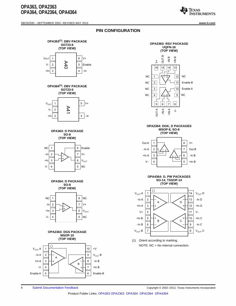
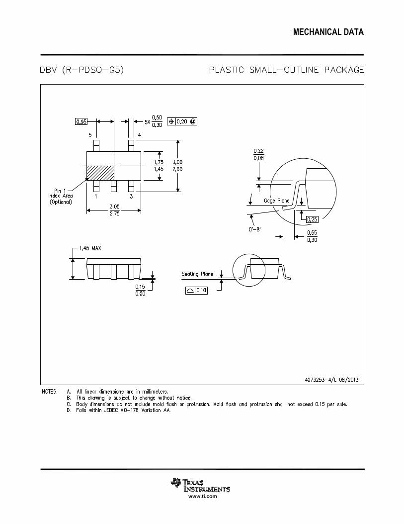
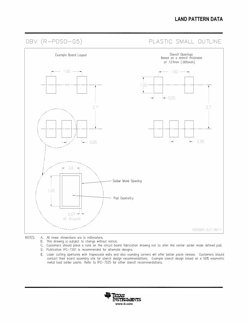
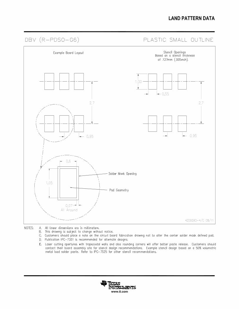
OPA363, OPA2363OPA364, OPA2364, OPA4364
SBOS259C –SEPTEMBER 2002–REVISED MAY 2013 www.ti.com
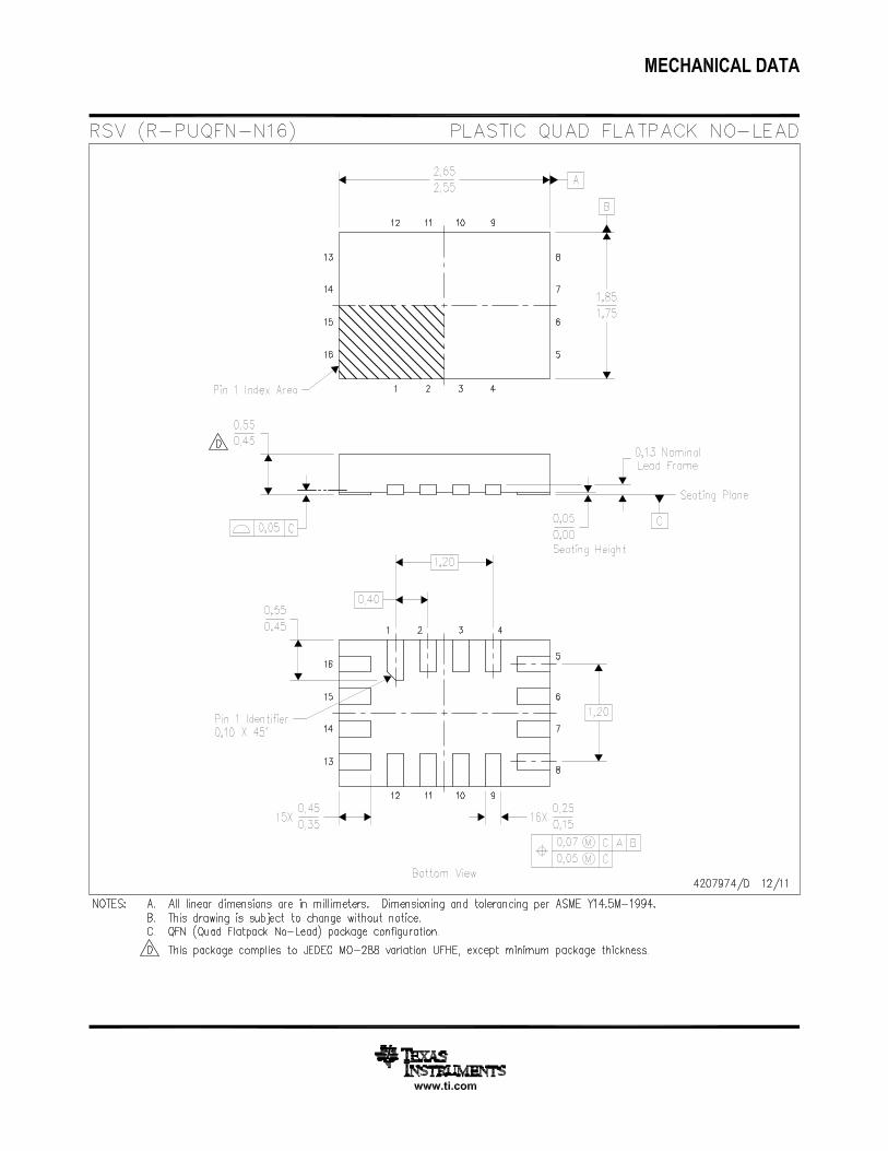
PIN CONFIGURATION
OPA363(1): DBV PACKAGEOPA2363: RSV PACKAGESOT23-6
UQFN-16(TOP VIEW)(TOP VIEW)
OPA364(1): DBV PACKAGESOT23-5
(TOP VIEW)
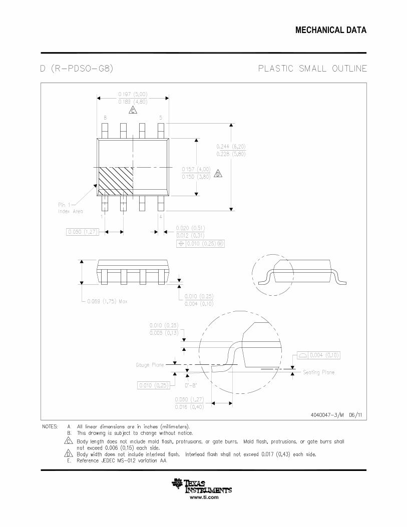
OPA2364: DGK, D PACKAGESMSOP-8, SO-8OPA363: D PACKAGE
(TOP VIEW)SO-8(TOP VIEW)
OPA4364: D, PW PACKAGESSO-14, TSSOP-14OPA364: D PACKAGE
(TOP VIEW)SO-8(TOP VIEW)
OPA2363: DGS PACKAGEMSOP-10
(TOP VIEW) (1) Orient according to marking.
NOTE: NC = No internal connection.
4 Submit Documentation Feedback Copyright © 2002–2013, Texas Instruments Incorporated
Product Folder Links: OPA363 OPA2363 OPA364 OPA2364 OPA4364
1
0.1
0.01
0.001
0.0001
Frequency (Hz)
TH
D+
N (
%)
10 100 1k 10k 100k
G = 10, R = 2kWL
V = 1.8VS
V = 10dBv-OUT G = 10, R = 2kWL
V = 5VS
G = 10, R = 10kWL
V = 1.8V, 5VS
G = 1, R = 2kWL
V = 1.8VS
G = 1,R = 2kWL
V = 5VS
G = 1,
R = 10kWL
V = 1.8V, 5VS
1
0.1
0.01
0.001
0.0001
Frequency (Hz)
TH
D+
N (
%)
10 100 1k 10k 100k
G = 10, R = 2kWL
G = 10, R = 10kWL
G = 1, R = 10kWLG = 1, R = 2kWL
(V = 5V, V = 1Vrms)S OUT
100
80
60
40
20
0
Frequency (Hz)
PS
RR
(dB
)
1 10 100 1k 10k 100k 10M1M
1.4
1.2
1.0
0.8
0.6
0.4
Supply Voltage (V)
Quie
scent C
urr
ent (m
A)
1.5 2.0 2.5 3.0 3.5 4.0 4.5 5.0 5.5 6.0
Per Amplifier
120
100
80
60
40
20
0
-20
Frequency (Hz)
Voltage G
ain
(dB
)
0
-30
-60
-90
-120
-150
-180
Phase (
)°
10 100 1k 10k 100k 1M 10M 100M
100
90
80
70
60
50
40
30
20
10
0
Frequency (Hz)
CM
RR
(dB
)
10 1k100 100k10k 1M 10M
OPA363, OPA2363OPA364, OPA2364, OPA4364
www.ti.com SBOS259C –SEPTEMBER 2002–REVISED MAY 2013
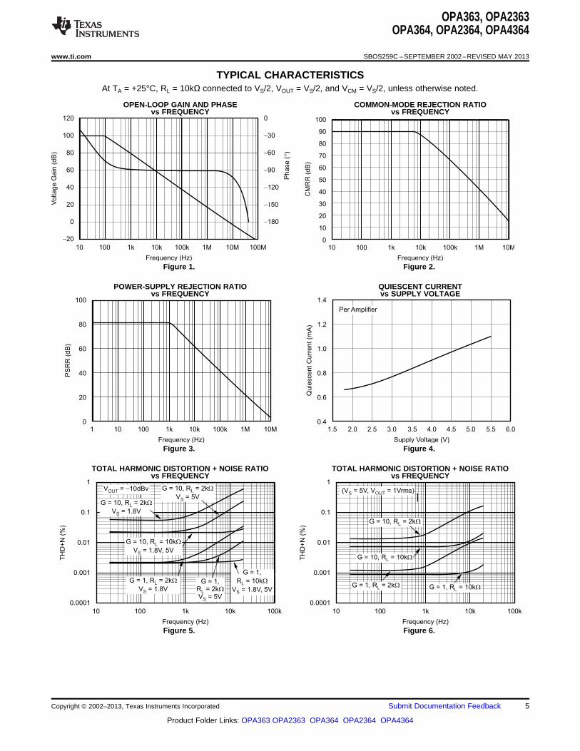
TYPICAL CHARACTERISTICSAt TA = +25°C, RL = 10kΩ connected to VS/2, VOUT = VS/2, and VCM = VS/2, unless otherwise noted.
OPEN-LOOP GAIN AND PHASE COMMON-MODE REJECTION RATIOvs FREQUENCY vs FREQUENCY
Figure 1. Figure 2.
POWER-SUPPLY REJECTION RATIO QUIESCENT CURRENTvs FREQUENCY vs SUPPLY VOLTAGE
Figure 3. Figure 4.
TOTAL HARMONIC DISTORTION + NOISE RATIO TOTAL HARMONIC DISTORTION + NOISE RATIOvs FREQUENCY vs FREQUENCY
Figure 5. Figure 6.
Copyright © 2002–2013, Texas Instruments Incorporated Submit Documentation Feedback 5
Product Folder Links: OPA363 OPA2363 OPA364 OPA2364 OPA4364
10k
1k
100
10
1
Temperature ( C)°
Input O
ffset C
urr
ent (p
A)
-50 -25 0 25 50 75 100 125
Temperature ( C)°
Input B
ias C
urr
ent (p
A)
-50 -25 0 25 50 75 100 125
10k
1k
100
10
1
3
2
1
0
-1
-2
-3
Output Current (mA)
Outp
ut V
oltage (
V)
0 ±10 ±20 ±30 ±40 ±50 ±60 ±70 ±80 ±90
T = 40 C- °A
V = 2.5VS ±V = 1.65VS ±
V = 0.9VS ±
V = 2.5VS ±V = 1.65VS ±
T = +25 C°A
T = +125 C°A
±100
4
2
0
-2
-4
-6
-8
-10
Common-Mode Voltage (V)
Input B
ias C
urr
ent (p
A)
-0.5 0.5 1.5 2.5 3.5 4.5 5.5
V = +5.1VCM
V = 0.1V-CM
1000
100
10
Frequency (Hz)
Input V
oltage N
ois
e (
nV
/)
ÖH
z
10 100 1k 10k 100k
120
100
80
60
40
20
0
Supply Voltage (V)
Short
-Circuit C
urr
ent (m
A)
1.5 2.0
+ISC
-ISC
2.5 3.0 3.5 4.0 4.5 5.0 5.5
OPA363, OPA2363OPA364, OPA2364, OPA4364
SBOS259C –SEPTEMBER 2002–REVISED MAY 2013 www.ti.com
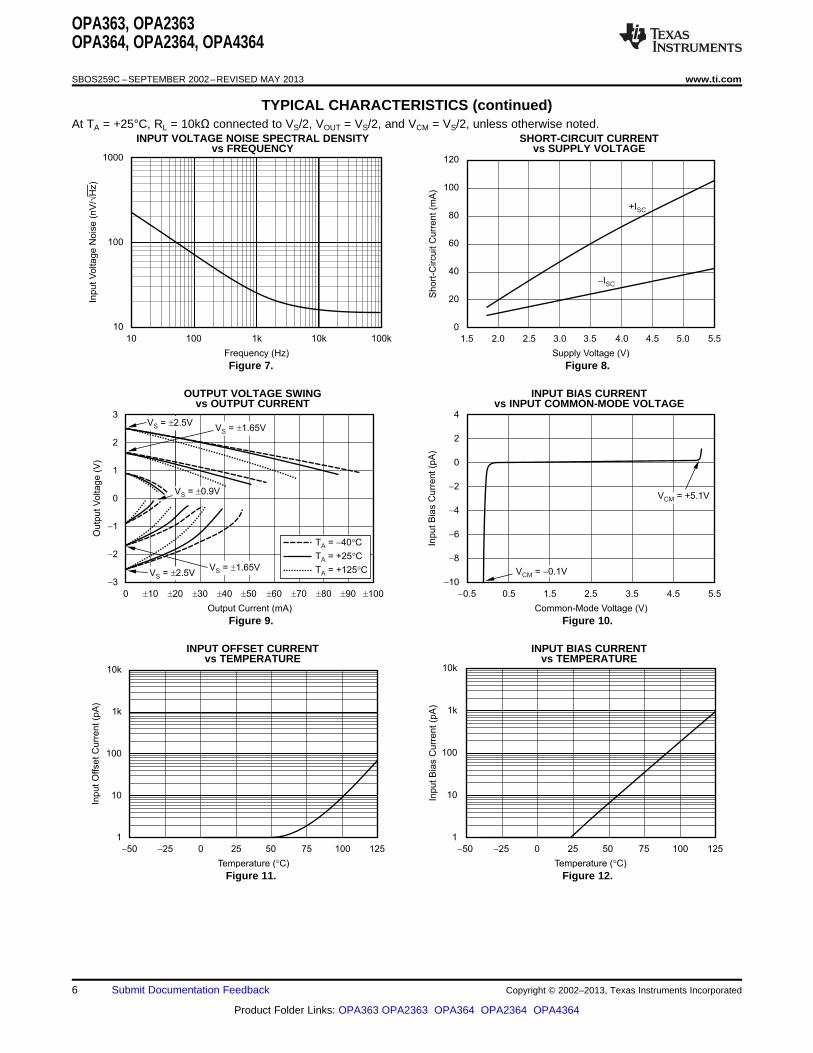
TYPICAL CHARACTERISTICS (continued)At TA = +25°C, RL = 10kΩ connected to VS/2, VOUT = VS/2, and VCM = VS/2, unless otherwise noted.
INPUT VOLTAGE NOISE SPECTRAL DENSITY SHORT-CIRCUIT CURRENTvs FREQUENCY vs SUPPLY VOLTAGE
Figure 7. Figure 8.
OUTPUT VOLTAGE SWING INPUT BIAS CURRENTvs OUTPUT CURRENT vs INPUT COMMON-MODE VOLTAGE
Figure 9. Figure 10.
INPUT OFFSET CURRENT INPUT BIAS CURRENTvs TEMPERATURE vs TEMPERATURE
Figure 11. Figure 12.
6 Submit Documentation Feedback Copyright © 2002–2013, Texas Instruments Incorporated
Product Folder Links: OPA363 OPA2363 OPA364 OPA2364 OPA4364

Frequency (Hz)
10 10k 100k 1M100 1k 10M
Channel S
epara
tion (
dB
)
130
120
110
100
90
80
70
60
50
40
VO
UT
VE
NA
BL
E
50 s/divm
Offset Voltage Drift ( V/ C)m °
0
Perc
ent ofA
mplif
iers
(%
)
20
15
10
5
0
1 2 3 4 5 6 7 8 9 > 10
Offset Voltage (mV)
Perc
ent ofA
mplif
iers
(%
)
16
14
12
10
8
6
4
2
0
Typical Production
Distribution of
Packaged Units
OPA36xAI
0 1.0 2.0 2.5-2.5 -2.0 -1.0
Load Capacitance (pF)
100
G = +1
1k
Overs
hoot (%
)
60
50
40
30
20
10
0
G = +10
Closed-Loop Gain (V/V)
1 10
0.01%
100
Settlin
gT
ime (
s)
m
100
10
1
0.1
0.1%
OPA363, OPA2363OPA364, OPA2364, OPA4364
www.ti.com SBOS259C –SEPTEMBER 2002–REVISED MAY 2013
TYPICAL CHARACTERISTICS (continued)At TA = +25°C, RL = 10kΩ connected to VS/2, VOUT = VS/2, and VCM = VS/2, unless otherwise noted.
SMALL-SIGNAL OVERSHOOT SETTLING TIMEvs LOAD CAPACITANCE vs CLOSED-LOOP GAIN
Figure 13. Figure 14.
OFFSET DRIFT DISTRIBUTION OFFSET VOLTAGE PRODUCTION DISTRIBUTION
Figure 15. Figure 16.
OUTPUT ENABLE CHARACTERISTIC(VS = 5V, VOUT = 20kHz Sinusoid) CHANNEL SEPARATION vs FREQUENCY
Figure 17. Figure 18.
Copyright © 2002–2013, Texas Instruments Incorporated Submit Documentation Feedback 7
Product Folder Links: OPA363 OPA2363 OPA364 OPA2364 OPA4364

Common-Mode Voltage (V)
-0.2 0 0.2 0.4 0.6 0.8 1.0 1.2 1.4 1.6 1.8 2.0
V(m
V)
OS
1.0
0.5
0
-0.5
-1.0
-1.5
-2.0
-2.5
-3.0
-3.5
Competitors
OPA363 and OPA364
1V
/div
1 s/divm
50m
V/d
iv
250ns/div
OPA363, OPA2363OPA364, OPA2364, OPA4364
SBOS259C –SEPTEMBER 2002–REVISED MAY 2013 www.ti.com
TYPICAL CHARACTERISTICS (continued)At TA = +25°C, RL = 10kΩ connected to VS/2, VOUT = VS/2, and VCM = VS/2, unless otherwise noted.
SMALL-SIGNAL STEP RESPONSE LARGE-SIGNAL STEP RESPONSE(CL = 100pF) (CL = 100pF)
Figure 19. Figure 20.
APPLICATION INFORMATION
The OPA363 and OPA364 series op amps are rail-to-rail operational amplifiers with excellent CMRR, low noise,low offset, and wide bandwidth on supply voltages as low as ±0.9V. The OPA363 features an additional pin forshutdown/ enable function. These families do not exhibit phase reversal and are unity-gain stable. Specified overthe industrial temperature range of –40°C to +125°C, the OPA363 and OPA364 families offer precisionperformance for a wide range of applications.
RAIL-TO-RAIL INPUT
The OPA363 and OPA364 feature excellent rail-to-rail operation, with supply voltages as low as ±0.9V. The inputcommon-mode voltage range of the OPA363 and OPA364 family extends 100mV beyond supply rails. Theunique input topology of the OPA363 and OPA364 eliminates the input offset transition region typical of most rail-to-rail complimentary stage operational amplifiers, allowing the OPA363 and OPA364 to provide superiorcommon-mode performance over the entire common-mode input range, as seen in Figure 21. This featureprevents degradation of the differential linearity error and THD when driving A/D converters. A simplifiedschematic of the OPA363 and OPA364 is shown in Figure 22.
Figure 21. OPA363 and OPA364 have Linear Offset Over Entire Common-Mode Range
8 Submit Documentation Feedback Copyright © 2002–2013, Texas Instruments Incorporated
Product Folder Links: OPA363 OPA2363 OPA364 OPA2364 OPA4364
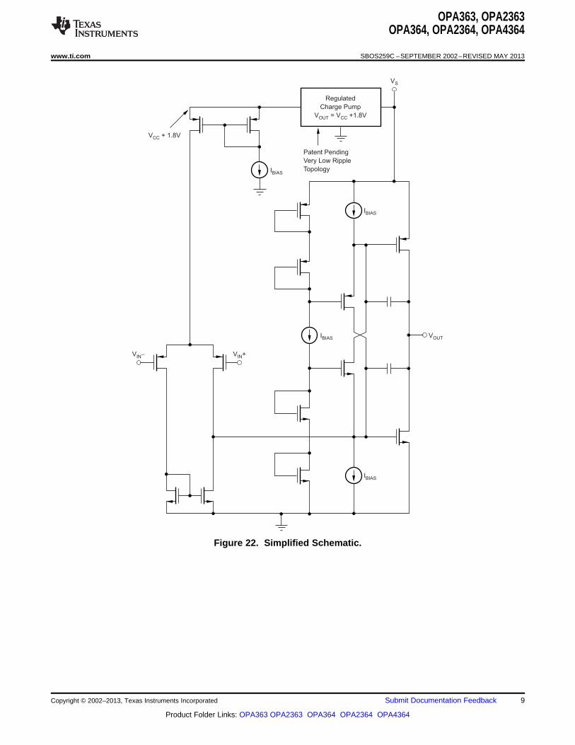
Regulated
Charge Pump
V = V +1.8VOUT CC
Patent Pending
Very Low Ripple
TopologyIBIAS
V + 1.8VCC
IBIAS
IBIAS
VS
IBIAS
VOUT
V -IN V +IN
OPA363, OPA2363OPA364, OPA2364, OPA4364
www.ti.com SBOS259C –SEPTEMBER 2002–REVISED MAY 2013
Figure 22. Simplified Schematic.
Copyright © 2002–2013, Texas Instruments Incorporated Submit Documentation Feedback 9
Product Folder Links: OPA363 OPA2363 OPA364 OPA2364 OPA4364
10 toW
20W
V+
VIN
VOUT
RS
RL
CL
OPAx363
OPAx364
OPA363, OPA2363OPA364, OPA2364, OPA4364
SBOS259C –SEPTEMBER 2002–REVISED MAY 2013 www.ti.com
OPERATING VOLTAGE
The OPA363 and OPA364 series op amp parameters are fully specified from +1.8V to +5.5V. Single 0.1μFbypass capacitors should be placed across supply pins and as close to the part as possible. Supply voltageshigher than 5.5V (absolute maximum) may cause permanent damage to the amplifier. Many specifications applyfrom –40°C to +125°C. Parameters that vary significantly with operating voltages or temperature are shown inthe Typical Characteristics.
ENABLE FUNCTION
The shutdown (enable) function of the OPA363 is referenced to the negative supply voltage of the operationalamplifier. A logic level HIGH enables the op amp. A valid logic HIGH is defined as voltage greater than 75% ofthe positive supply applied to the enable pin. The valid logic HIGH signal can be as much as 5.5V above thenegative supply, independent of the positive supply voltage. A valid logic LOW is defined as less than 0.8Vabove the negative supply pin. If dual or split power supplies are used, care should be taken to ensure logic inputsignals are properly referred to the negative supply voltage. This pin should be connected to a valid high or lowvoltage or driven, not left open circuit.
The logic input is a high-impedance CMOS input. Dual op amps are provided separate logic inputs. For battery-operated applications, this feature may be used to greatly reduce the average current and extend battery life.The enable time is 20μs; disable time is 1μs. When disabled, the output assumes a high-impedance state. Thisallows the OPA363 to be operated as a “gated” amplifier, or to have its output multiplexed onto a commonanalog output bus.
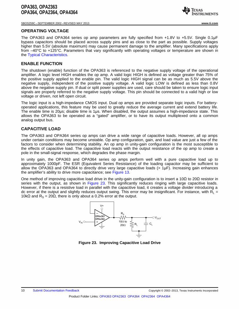
CAPACITIVE LOAD
The OPA363 and OPA364 series op amps can drive a wide range of capacitive loads. However, all op ampsunder certain conditions may become unstable. Op amp configuration, gain, and load value are just a few of thefactors to consider when determining stability. An op amp in unity-gain configuration is the most susceptible tothe effects of capacitive load. The capacitive load reacts with the output resistance of the op amp to create apole in the small-signal response, which degrades the phase margin.
In unity gain, the OPA363 and OPA364 series op amps perform well with a pure capacitive load up toapproximately 1000pF. The ESR (Equivalent Series Resistance) of the loading capacitor may be sufficient toallow the OPA363 and OPA364 to directly drive very large capacitive loads (> 1μF). Increasing gain enhancesthe amplifier’s ability to drive more capacitance; see Figure 13.
One method of improving capacitive load drive in the unity-gain configuration is to insert a 10Ω to 20Ω resistor inseries with the output, as shown in Figure 23. This significantly reduces ringing with large capacitive loads.However, if there is a resistive load in parallel with the capacitive load, it creates a voltage divider introducing adc error at the output and slightly reduces output swing. This error may be insignificant. For instance, with RL =10kΩ and RS = 20Ω, there is only about a 0.2% error at the output.
Figure 23. Improving Capacitive Load Drive
10 Submit Documentation Feedback Copyright © 2002–2013, Texas Instruments Incorporated
Product Folder Links: OPA363 OPA2363 OPA364 OPA2364 OPA4364
VOUT
R = 10kWP500 Am
OPA363
OPA364
VIN
V+ = +5V
Op Amp
Negative
Supply
Grounded
-V = 5V-
(Additional
Negative Supply)
5kW
OPAx36310mA max
V+
VIN
VOUT
IOVERLOAD
OPA363, OPA2363OPA364, OPA2364, OPA4364
www.ti.com SBOS259C –SEPTEMBER 2002–REVISED MAY 2013
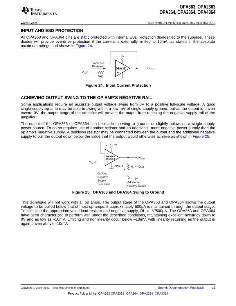
INPUT AND ESD PROTECTION
All OPA363 and OPA364 pins are static protected with internal ESD protection diodes tied to the supplies. Thesediodes will provide overdrive protection if the current is externally limited to 10mA, as stated in the absolutemaximum ratings and shown in Figure 24.
Figure 24. Input Current Protection
ACHIEVING OUTPUT SWING TO THE OP AMP’S NEGATIVE RAIL
Some applications require an accurate output voltage swing from 0V to a positive full-scale voltage. A goodsingle supply op amp may be able to swing within a few mV of single supply ground, but as the output is driventoward 0V, the output stage of the amplifier will prevent the output from reaching the negative supply rail of theamplifier.
The output of the OPA363 or OPA364 can be made to swing to ground, or slightly below, on a single supplypower source. To do so requires use of another resistor and an additional, more negative power supply than theop amp’s negative supply. A pulldown resistor may be connected between the output and the additional negativesupply to pull the output down below the value that the output would otherwise achieve as shown in Figure 25.
Figure 25. OPA363 and OPA364 Swing to Ground
This technique will not work with all op amps. The output stage of the OPA363 and OPA364 allows the outputvoltage to be pulled below that of most op amps, if approximately 500μA is maintained through the output stage.To calculate the appropriate value load resistor and negative supply, RL = –V/500μA. The OPA363 and OPA364have been characterized to perform well under the described conditions, maintaining excellent accuracy down to0V and as low as –10mV. Limiting and nonlinearity occur below –10mV, with linearity returning as the output isagain driven above –10mV.
Copyright © 2002–2013, Texas Instruments Incorporated Submit Documentation Feedback 11
Product Folder Links: OPA363 OPA2363 OPA364 OPA2364 OPA4364
MSP430
V+
V+
VIN
100W
1nF
OPA363
OPA364
ADS8324
V+ = 1.8V
V+ = 1.8V
OPA363
OPA364
VIN
100W
1nF
V+
R1
10kW
R2
10kW
0.9V
OPAx363
OPAx364
V+
C = 1 FmL
OPA363, OPA2363OPA364, OPA2364, OPA4364
SBOS259C –SEPTEMBER 2002–REVISED MAY 2013 www.ti.com
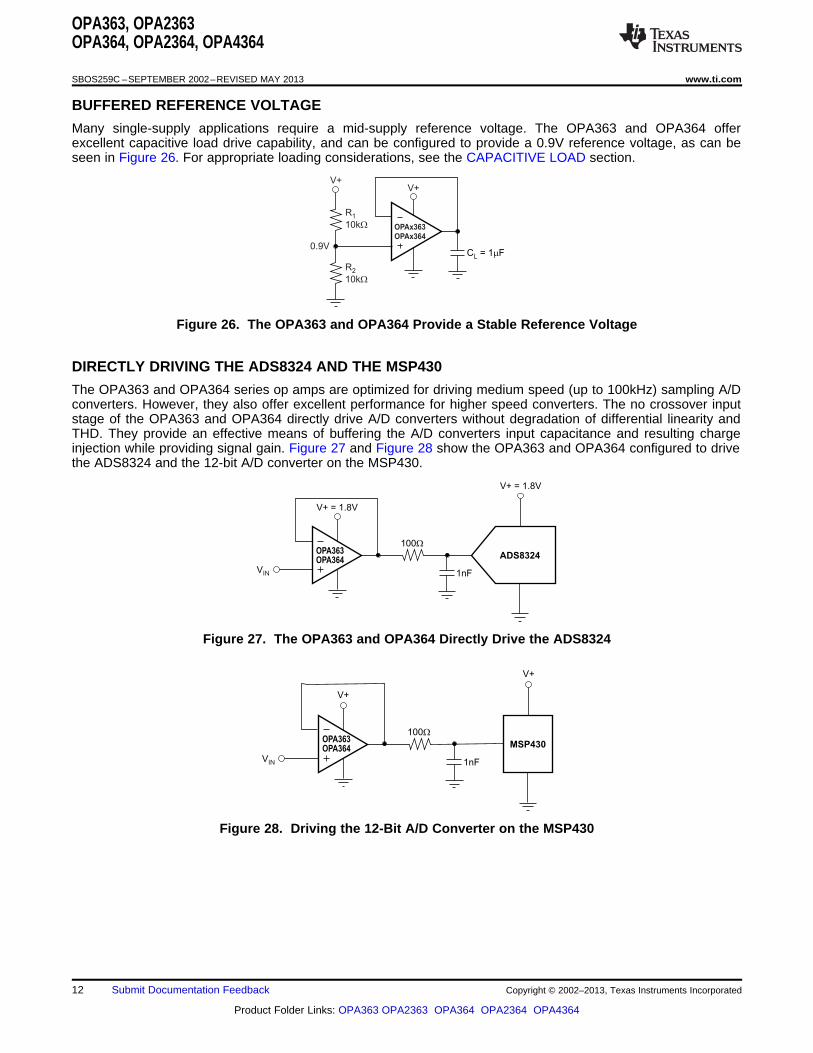
BUFFERED REFERENCE VOLTAGE
Many single-supply applications require a mid-supply reference voltage. The OPA363 and OPA364 offerexcellent capacitive load drive capability, and can be configured to provide a 0.9V reference voltage, as can beseen in Figure 26. For appropriate loading considerations, see the CAPACITIVE LOAD section.
Figure 26. The OPA363 and OPA364 Provide a Stable Reference Voltage
DIRECTLY DRIVING THE ADS8324 AND THE MSP430
The OPA363 and OPA364 series op amps are optimized for driving medium speed (up to 100kHz) sampling A/Dconverters. However, they also offer excellent performance for higher speed converters. The no crossover inputstage of the OPA363 and OPA364 directly drive A/D converters without degradation of differential linearity andTHD. They provide an effective means of buffering the A/D converters input capacitance and resulting chargeinjection while providing signal gain. Figure 27 and Figure 28 show the OPA363 and OPA364 configured to drivethe ADS8324 and the 12-bit A/D converter on the MSP430.
Figure 27. The OPA363 and OPA364 Directly Drive the ADS8324
Figure 28. Driving the 12-Bit A/D Converter on the MSP430
12 Submit Documentation Feedback Copyright © 2002–2013, Texas Instruments Incorporated
Product Folder Links: OPA363 OPA2363 OPA364 OPA2364 OPA4364
3.3V
49kW
VOUT
OPAx363
OPAx364
Clean 3.3V Supply
1 Fm
4kW
6kWElectret
Microphone
5kW
V+
V-
20kW
1/2
OPA2363
One of Right or Left Channel
One of Right or Left
Headphone Out
10kW
20kW
V+
V-
Internally
Biased
20kW
1/2
TPS6100
20kW
10kW
1 Fm
47pF
V-
OPA363, OPA2363OPA364, OPA2364, OPA4364
www.ti.com SBOS259C –SEPTEMBER 2002–REVISED MAY 2013
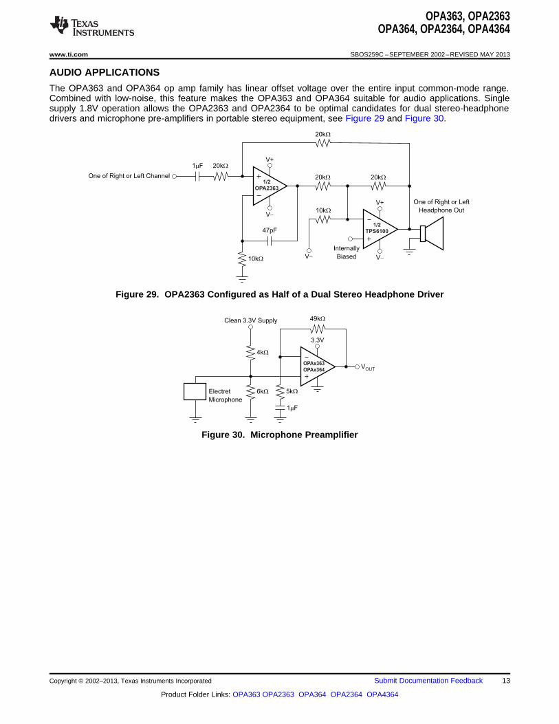
AUDIO APPLICATIONS
The OPA363 and OPA364 op amp family has linear offset voltage over the entire input common-mode range.Combined with low-noise, this feature makes the OPA363 and OPA364 suitable for audio applications. Singlesupply 1.8V operation allows the OPA2363 and OPA2364 to be optimal candidates for dual stereo-headphonedrivers and microphone pre-amplifiers in portable stereo equipment, see Figure 29 and Figure 30.
Figure 29. OPA2363 Configured as Half of a Dual Stereo Headphone Driver
Figure 30. Microphone Preamplifier
Copyright © 2002–2013, Texas Instruments Incorporated Submit Documentation Feedback 13
Product Folder Links: OPA363 OPA2363 OPA364 OPA2364 OPA4364

VOUT
V = 1VrmsIN
OPA363
150kW19.5kW
220pF
1.8kW
3.3nF 47pF
R11
3.92kW
R12
3.92kW
C13
1000pF
R14
3.48kW
C15
1000pF
VOUTVIN
R1
3.92kW
R3
1.33kW
C4
1000pF
1/2
OPA2363
1/2
OPA2363
3
2
1
6
5
7
2
3
6OPA363
OPA363, OPA2363OPA364, OPA2364, OPA4364
SBOS259C –SEPTEMBER 2002–REVISED MAY 2013 www.ti.com
ACTIVE FILTERING
Low harmonic distortion and noise specifications plus high gain and slew rate make the OPA363 and OPA364optimal candidates for active filtering. Figure 31 shows the OPA2363 configured as a low-distortion, 3rd-orderGIC (General Immittance Converter) filter. Figure 32 shows the implementation of a Sallen-Key, 3-pole, low-passBessel filter.
Figure 31. The OPA2363 as a 3rd-Order, 40kHz, Low-Pass GIC Filter
Figure 32. The OPA363 or OPA364 Configured as a 3-Pole, 20kHz, Sallen-Key Filter
14 Submit Documentation Feedback Copyright © 2002–2013, Texas Instruments Incorporated
Product Folder Links: OPA363 OPA2363 OPA364 OPA2364 OPA4364
OPA363, OPA2363OPA364, OPA2364, OPA4364
www.ti.com SBOS259C –SEPTEMBER 2002–REVISED MAY 2013
REVISION HISTORY
NOTE: Page numbers for previous versions may differ from page numbers in the current version.
Changes from Revision B (February 2003) to Revision C Page
• Converted data sheet to current format ................................................................................................................................ 1
• Added RSV package (UQFN-16) to data sheet .................................................................................................................... 1
Copyright © 2002–2013, Texas Instruments Incorporated Submit Documentation Feedback 15
Product Folder Links: OPA363 OPA2363 OPA364 OPA2364 OPA4364
PACKAGE OPTION ADDENDUM
www.ti.com 7-Nov-2014
Addendum-Page 1
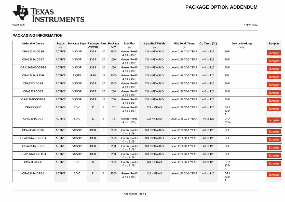
PACKAGING INFORMATION
Orderable Device Status(1)
Package Type PackageDrawing
Pins PackageQty
Eco Plan(2)
Lead/Ball Finish(6)
MSL Peak Temp(3)
Op Temp (°C) Device Marking(4/5)
Samples
OPA2363AIDGSR ACTIVE VSSOP DGS 10 2500 Green (RoHS& no Sb/Br)
CU NIPDAUAG Level-2-260C-1 YEAR -40 to 125 BHK
OPA2363AIDGST ACTIVE VSSOP DGS 10 250 Green (RoHS& no Sb/Br)
CU NIPDAUAG Level-2-260C-1 YEAR -40 to 125 BHK
OPA2363AIDGSTG4 ACTIVE VSSOP DGS 10 250 Green (RoHS& no Sb/Br)
CU NIPDAUAG Level-2-260C-1 YEAR -40 to 125 BHK
OPA2363AIRSVR ACTIVE UQFN RSV 16 3000 Green (RoHS& no Sb/Br)
CU NIPDAUAG Level-2-260C-1 YEAR -40 to 125 SIN
OPA2363IDGSR ACTIVE VSSOP DGS 10 2500 Green (RoHS& no Sb/Br)
CU NIPDAUAG Level-2-260C-1 YEAR -40 to 125 BHK
OPA2363IDGST ACTIVE VSSOP DGS 10 250 Green (RoHS& no Sb/Br)
CU NIPDAUAG Level-2-260C-1 YEAR -40 to 125 BHK
OPA2363IDGSTG4 ACTIVE VSSOP DGS 10 250 Green (RoHS& no Sb/Br)
CU NIPDAUAG Level-2-260C-1 YEAR -40 to 125 BHK
OPA2364AID ACTIVE SOIC D 8 75 Green (RoHS& no Sb/Br)
CU NIPDAU Level-2-260C-1 YEAR -40 to 125 OPA2364A
OPA2364AIDG4 ACTIVE SOIC D 8 75 Green (RoHS& no Sb/Br)
CU NIPDAU Level-2-260C-1 YEAR -40 to 125 OPA2364A
OPA2364AIDGKR ACTIVE VSSOP DGK 8 2500 Green (RoHS& no Sb/Br)
CU NIPDAUAG Level-2-260C-1 YEAR -40 to 125 BHL
OPA2364AIDGKRG4 ACTIVE VSSOP DGK 8 2500 Green (RoHS& no Sb/Br)
CU NIPDAUAG Level-2-260C-1 YEAR -40 to 125 BHL
OPA2364AIDGKT ACTIVE VSSOP DGK 8 250 Green (RoHS& no Sb/Br)
CU NIPDAUAG Level-2-260C-1 YEAR -40 to 125 BHL
OPA2364AIDGKTG4 ACTIVE VSSOP DGK 8 250 Green (RoHS& no Sb/Br)
CU NIPDAUAG Level-2-260C-1 YEAR -40 to 125 BHL
OPA2364AIDR ACTIVE SOIC D 8 2500 Green (RoHS& no Sb/Br)
CU NIPDAU Level-2-260C-1 YEAR -40 to 125 OPA2364A
OPA2364AIDRG4 ACTIVE SOIC D 8 2500 Green (RoHS& no Sb/Br)
CU NIPDAU Level-2-260C-1 YEAR -40 to 125 OPA2364A
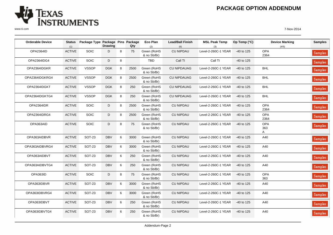
PACKAGE OPTION ADDENDUM
www.ti.com 7-Nov-2014
Addendum-Page 2
Orderable Device Status(1)
Package Type PackageDrawing
Pins PackageQty
Eco Plan(2)
Lead/Ball Finish(6)
MSL Peak Temp(3)
Op Temp (°C) Device Marking(4/5)
Samples
OPA2364ID ACTIVE SOIC D 8 75 Green (RoHS& no Sb/Br)
CU NIPDAU Level-2-260C-1 YEAR -40 to 125 OPA2364
OPA2364IDG4 ACTIVE SOIC D 8 TBD Call TI Call TI -40 to 125
OPA2364IDGKR ACTIVE VSSOP DGK 8 2500 Green (RoHS& no Sb/Br)
CU NIPDAUAG Level-2-260C-1 YEAR -40 to 125 BHL
OPA2364IDGKRG4 ACTIVE VSSOP DGK 8 2500 Green (RoHS& no Sb/Br)
CU NIPDAUAG Level-2-260C-1 YEAR -40 to 125 BHL
OPA2364IDGKT ACTIVE VSSOP DGK 8 250 Green (RoHS& no Sb/Br)
CU NIPDAUAG Level-2-260C-1 YEAR -40 to 125 BHL
OPA2364IDGKTG4 ACTIVE VSSOP DGK 8 250 Green (RoHS& no Sb/Br)
CU NIPDAUAG Level-2-260C-1 YEAR -40 to 125 BHL
OPA2364IDR ACTIVE SOIC D 8 2500 Green (RoHS& no Sb/Br)
CU NIPDAU Level-2-260C-1 YEAR -40 to 125 OPA2364
OPA2364IDRG4 ACTIVE SOIC D 8 2500 Green (RoHS& no Sb/Br)
CU NIPDAU Level-2-260C-1 YEAR -40 to 125 OPA2364
OPA363AID ACTIVE SOIC D 8 75 Green (RoHS& no Sb/Br)
CU NIPDAU Level-2-260C-1 YEAR -40 to 125 OPA363A
OPA363AIDBVR ACTIVE SOT-23 DBV 6 3000 Green (RoHS& no Sb/Br)
CU NIPDAU Level-2-260C-1 YEAR -40 to 125 A40
OPA363AIDBVRG4 ACTIVE SOT-23 DBV 6 3000 Green (RoHS& no Sb/Br)
CU NIPDAU Level-2-260C-1 YEAR -40 to 125 A40
OPA363AIDBVT ACTIVE SOT-23 DBV 6 250 Green (RoHS& no Sb/Br)
CU NIPDAU Level-2-260C-1 YEAR -40 to 125 A40
OPA363AIDBVTG4 ACTIVE SOT-23 DBV 6 250 Green (RoHS& no Sb/Br)
CU NIPDAU Level-2-260C-1 YEAR -40 to 125 A40
OPA363ID ACTIVE SOIC D 8 75 Green (RoHS& no Sb/Br)
CU NIPDAU Level-2-260C-1 YEAR -40 to 125 OPA363
OPA363IDBVR ACTIVE SOT-23 DBV 6 3000 Green (RoHS& no Sb/Br)
CU NIPDAU Level-2-260C-1 YEAR -40 to 125 A40
OPA363IDBVRG4 ACTIVE SOT-23 DBV 6 3000 Green (RoHS& no Sb/Br)
CU NIPDAU Level-2-260C-1 YEAR -40 to 125 A40
OPA363IDBVT ACTIVE SOT-23 DBV 6 250 Green (RoHS& no Sb/Br)
CU NIPDAU Level-2-260C-1 YEAR -40 to 125 A40
OPA363IDBVTG4 ACTIVE SOT-23 DBV 6 250 Green (RoHS& no Sb/Br)
CU NIPDAU Level-2-260C-1 YEAR -40 to 125 A40
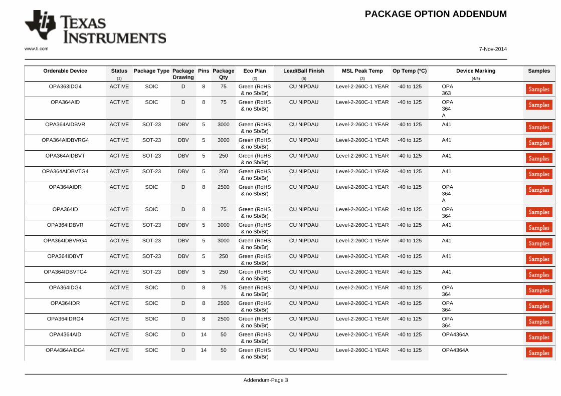
PACKAGE OPTION ADDENDUM
www.ti.com 7-Nov-2014
Addendum-Page 3
Orderable Device Status(1)
Package Type PackageDrawing
Pins PackageQty
Eco Plan(2)
Lead/Ball Finish(6)
MSL Peak Temp(3)
Op Temp (°C) Device Marking(4/5)
Samples
OPA363IDG4 ACTIVE SOIC D 8 75 Green (RoHS& no Sb/Br)
CU NIPDAU Level-2-260C-1 YEAR -40 to 125 OPA363
OPA364AID ACTIVE SOIC D 8 75 Green (RoHS& no Sb/Br)
CU NIPDAU Level-2-260C-1 YEAR -40 to 125 OPA364A
OPA364AIDBVR ACTIVE SOT-23 DBV 5 3000 Green (RoHS& no Sb/Br)
CU NIPDAU Level-2-260C-1 YEAR -40 to 125 A41
OPA364AIDBVRG4 ACTIVE SOT-23 DBV 5 3000 Green (RoHS& no Sb/Br)
CU NIPDAU Level-2-260C-1 YEAR -40 to 125 A41
OPA364AIDBVT ACTIVE SOT-23 DBV 5 250 Green (RoHS& no Sb/Br)
CU NIPDAU Level-2-260C-1 YEAR -40 to 125 A41
OPA364AIDBVTG4 ACTIVE SOT-23 DBV 5 250 Green (RoHS& no Sb/Br)
CU NIPDAU Level-2-260C-1 YEAR -40 to 125 A41
OPA364AIDR ACTIVE SOIC D 8 2500 Green (RoHS& no Sb/Br)
CU NIPDAU Level-2-260C-1 YEAR -40 to 125 OPA364A
OPA364ID ACTIVE SOIC D 8 75 Green (RoHS& no Sb/Br)
CU NIPDAU Level-2-260C-1 YEAR -40 to 125 OPA364
OPA364IDBVR ACTIVE SOT-23 DBV 5 3000 Green (RoHS& no Sb/Br)
CU NIPDAU Level-2-260C-1 YEAR -40 to 125 A41
OPA364IDBVRG4 ACTIVE SOT-23 DBV 5 3000 Green (RoHS& no Sb/Br)
CU NIPDAU Level-2-260C-1 YEAR -40 to 125 A41
OPA364IDBVT ACTIVE SOT-23 DBV 5 250 Green (RoHS& no Sb/Br)
CU NIPDAU Level-2-260C-1 YEAR -40 to 125 A41
OPA364IDBVTG4 ACTIVE SOT-23 DBV 5 250 Green (RoHS& no Sb/Br)
CU NIPDAU Level-2-260C-1 YEAR -40 to 125 A41
OPA364IDG4 ACTIVE SOIC D 8 75 Green (RoHS& no Sb/Br)
CU NIPDAU Level-2-260C-1 YEAR -40 to 125 OPA364
OPA364IDR ACTIVE SOIC D 8 2500 Green (RoHS& no Sb/Br)
CU NIPDAU Level-2-260C-1 YEAR -40 to 125 OPA364
OPA364IDRG4 ACTIVE SOIC D 8 2500 Green (RoHS& no Sb/Br)
CU NIPDAU Level-2-260C-1 YEAR -40 to 125 OPA364
OPA4364AID ACTIVE SOIC D 14 50 Green (RoHS& no Sb/Br)
CU NIPDAU Level-2-260C-1 YEAR -40 to 125 OPA4364A
OPA4364AIDG4 ACTIVE SOIC D 14 50 Green (RoHS& no Sb/Br)
CU NIPDAU Level-2-260C-1 YEAR -40 to 125 OPA4364A

PACKAGE OPTION ADDENDUM
www.ti.com 7-Nov-2014
Addendum-Page 4
Orderable Device Status(1)
Package Type PackageDrawing
Pins PackageQty
Eco Plan(2)
Lead/Ball Finish(6)
MSL Peak Temp(3)
Op Temp (°C) Device Marking(4/5)
Samples
OPA4364AIDR ACTIVE SOIC D 14 2500 Green (RoHS& no Sb/Br)
CU NIPDAU Level-2-260C-1 YEAR -40 to 125 OPA4364A
OPA4364AIDRG4 ACTIVE SOIC D 14 2500 Green (RoHS& no Sb/Br)
CU NIPDAU Level-2-260C-1 YEAR -40 to 125 OPA4364A
OPA4364AIPWR ACTIVE TSSOP PW 14 2500 Green (RoHS& no Sb/Br)
CU NIPDAU Level-2-260C-1 YEAR -40 to 125 OPA4364A
OPA4364AIPWRG4 ACTIVE TSSOP PW 14 2500 Green (RoHS& no Sb/Br)
CU NIPDAU Level-2-260C-1 YEAR -40 to 125 OPA4364A
OPA4364AIPWT ACTIVE TSSOP PW 14 250 Green (RoHS& no Sb/Br)
CU NIPDAU Level-2-260C-1 YEAR -40 to 125 OPA4364A
OPA4364AIPWTG4 ACTIVE TSSOP PW 14 250 Green (RoHS& no Sb/Br)
CU NIPDAU Level-2-260C-1 YEAR -40 to 125 OPA4364A
(1) The marketing status values are defined as follows:ACTIVE: Product device recommended for new designs.LIFEBUY: TI has announced that the device will be discontinued, and a lifetime-buy period is in effect.NRND: Not recommended for new designs. Device is in production to support existing customers, but TI does not recommend using this part in a new design.PREVIEW: Device has been announced but is not in production. Samples may or may not be available.OBSOLETE: TI has discontinued the production of the device.
(2) Eco Plan - The planned eco-friendly classification: Pb-Free (RoHS), Pb-Free (RoHS Exempt), or Green (RoHS & no Sb/Br) - please check http://www.ti.com/productcontent for the latest availabilityinformation and additional product content details.TBD: The Pb-Free/Green conversion plan has not been defined.Pb-Free (RoHS): TI's terms "Lead-Free" or "Pb-Free" mean semiconductor products that are compatible with the current RoHS requirements for all 6 substances, including the requirement thatlead not exceed 0.1% by weight in homogeneous materials. Where designed to be soldered at high temperatures, TI Pb-Free products are suitable for use in specified lead-free processes.Pb-Free (RoHS Exempt): This component has a RoHS exemption for either 1) lead-based flip-chip solder bumps used between the die and package, or 2) lead-based die adhesive used betweenthe die and leadframe. The component is otherwise considered Pb-Free (RoHS compatible) as defined above.Green (RoHS & no Sb/Br): TI defines "Green" to mean Pb-Free (RoHS compatible), and free of Bromine (Br) and Antimony (Sb) based flame retardants (Br or Sb do not exceed 0.1% by weightin homogeneous material)
(3) MSL, Peak Temp. - The Moisture Sensitivity Level rating according to the JEDEC industry standard classifications, and peak solder temperature.
(4) There may be additional marking, which relates to the logo, the lot trace code information, or the environmental category on the device.
(5) Multiple Device Markings will be inside parentheses. Only one Device Marking contained in parentheses and separated by a "~" will appear on a device. If a line is indented then it is a continuationof the previous line and the two combined represent the entire Device Marking for that device.

PACKAGE OPTION ADDENDUM
www.ti.com 7-Nov-2014
Addendum-Page 5
(6) Lead/Ball Finish - Orderable Devices may have multiple material finish options. Finish options are separated by a vertical ruled line. Lead/Ball Finish values may wrap to two lines if the finishvalue exceeds the maximum column width.
Important Information and Disclaimer:The information provided on this page represents TI's knowledge and belief as of the date that it is provided. TI bases its knowledge and belief on informationprovided by third parties, and makes no representation or warranty as to the accuracy of such information. Efforts are underway to better integrate information from third parties. TI has taken andcontinues to take reasonable steps to provide representative and accurate information but may not have conducted destructive testing or chemical analysis on incoming materials and chemicals.TI and TI suppliers consider certain information to be proprietary, and thus CAS numbers and other limited information may not be available for release.
In no event shall TI's liability arising out of such information exceed the total purchase price of the TI part(s) at issue in this document sold by TI to Customer on an annual basis.
OTHER QUALIFIED VERSIONS OF OPA4364 :
• Automotive: OPA4364-Q1
NOTE: Qualified Version Definitions:
• Automotive - Q100 devices qualified for high-reliability automotive applications targeting zero defects
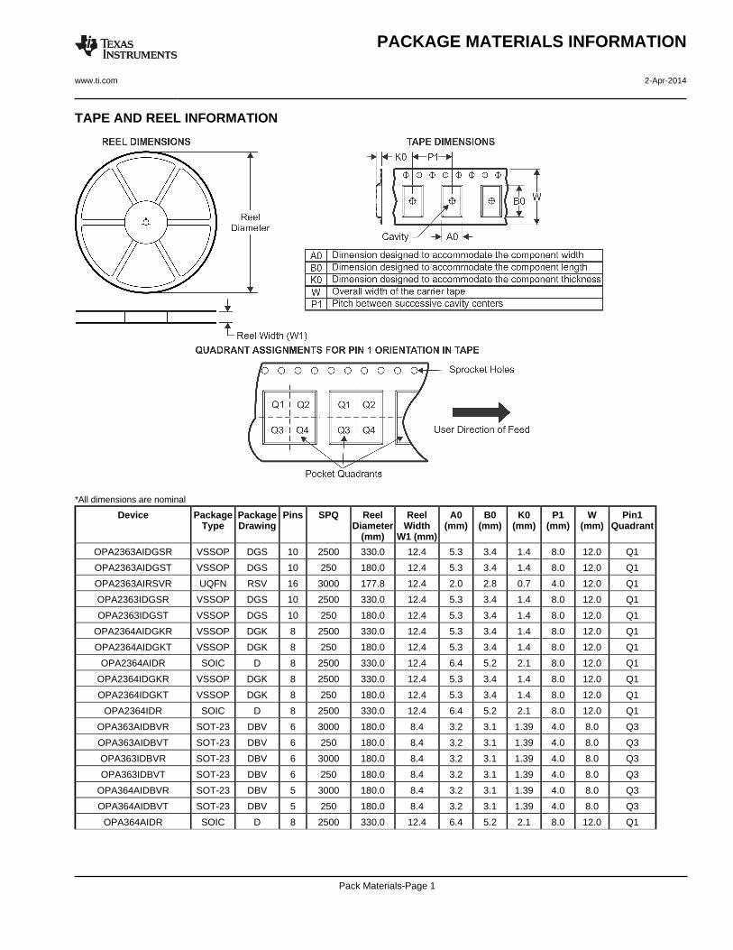
TAPE AND REEL INFORMATION
*All dimensions are nominal
Device PackageType
PackageDrawing
Pins SPQ ReelDiameter
(mm)
ReelWidth
W1 (mm)
A0(mm)
B0(mm)
K0(mm)
P1(mm)
W(mm)
Pin1Quadrant
OPA2363AIDGSR VSSOP DGS 10 2500 330.0 12.4 5.3 3.4 1.4 8.0 12.0 Q1
OPA2363AIDGST VSSOP DGS 10 250 180.0 12.4 5.3 3.4 1.4 8.0 12.0 Q1
OPA2363AIRSVR UQFN RSV 16 3000 177.8 12.4 2.0 2.8 0.7 4.0 12.0 Q1
OPA2363IDGSR VSSOP DGS 10 2500 330.0 12.4 5.3 3.4 1.4 8.0 12.0 Q1
OPA2363IDGST VSSOP DGS 10 250 180.0 12.4 5.3 3.4 1.4 8.0 12.0 Q1
OPA2364AIDGKR VSSOP DGK 8 2500 330.0 12.4 5.3 3.4 1.4 8.0 12.0 Q1
OPA2364AIDGKT VSSOP DGK 8 250 180.0 12.4 5.3 3.4 1.4 8.0 12.0 Q1
OPA2364AIDR SOIC D 8 2500 330.0 12.4 6.4 5.2 2.1 8.0 12.0 Q1
OPA2364IDGKR VSSOP DGK 8 2500 330.0 12.4 5.3 3.4 1.4 8.0 12.0 Q1
OPA2364IDGKT VSSOP DGK 8 250 180.0 12.4 5.3 3.4 1.4 8.0 12.0 Q1
OPA2364IDR SOIC D 8 2500 330.0 12.4 6.4 5.2 2.1 8.0 12.0 Q1
OPA363AIDBVR SOT-23 DBV 6 3000 180.0 8.4 3.2 3.1 1.39 4.0 8.0 Q3
OPA363AIDBVT SOT-23 DBV 6 250 180.0 8.4 3.2 3.1 1.39 4.0 8.0 Q3
OPA363IDBVR SOT-23 DBV 6 3000 180.0 8.4 3.2 3.1 1.39 4.0 8.0 Q3
OPA363IDBVT SOT-23 DBV 6 250 180.0 8.4 3.2 3.1 1.39 4.0 8.0 Q3
OPA364AIDBVR SOT-23 DBV 5 3000 180.0 8.4 3.2 3.1 1.39 4.0 8.0 Q3
OPA364AIDBVT SOT-23 DBV 5 250 180.0 8.4 3.2 3.1 1.39 4.0 8.0 Q3
OPA364AIDR SOIC D 8 2500 330.0 12.4 6.4 5.2 2.1 8.0 12.0 Q1
PACKAGE MATERIALS INFORMATION
www.ti.com 2-Apr-2014
Pack Materials-Page 1
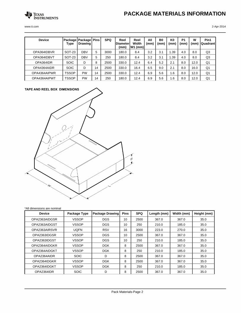
Device PackageType
PackageDrawing
Pins SPQ ReelDiameter
(mm)
ReelWidth
W1 (mm)
A0(mm)
B0(mm)
K0(mm)
P1(mm)
W(mm)
Pin1Quadrant
OPA364IDBVR SOT-23 DBV 5 3000 180.0 8.4 3.2 3.1 1.39 4.0 8.0 Q3
OPA364IDBVT SOT-23 DBV 5 250 180.0 8.4 3.2 3.1 1.39 4.0 8.0 Q3
OPA364IDR SOIC D 8 2500 330.0 12.4 6.4 5.2 2.1 8.0 12.0 Q1
OPA4364AIDR SOIC D 14 2500 330.0 16.4 6.5 9.0 2.1 8.0 16.0 Q1
OPA4364AIPWR TSSOP PW 14 2500 330.0 12.4 6.9 5.6 1.6 8.0 12.0 Q1
OPA4364AIPWT TSSOP PW 14 250 180.0 12.4 6.9 5.6 1.6 8.0 12.0 Q1
*All dimensions are nominal
Device Package Type Package Drawing Pins SPQ Length (mm) Width (mm) Height (mm)
OPA2363AIDGSR VSSOP DGS 10 2500 367.0 367.0 35.0
OPA2363AIDGST VSSOP DGS 10 250 210.0 185.0 35.0
OPA2363AIRSVR UQFN RSV 16 3000 223.0 270.0 35.0
OPA2363IDGSR VSSOP DGS 10 2500 367.0 367.0 35.0
OPA2363IDGST VSSOP DGS 10 250 210.0 185.0 35.0
OPA2364AIDGKR VSSOP DGK 8 2500 367.0 367.0 35.0
OPA2364AIDGKT VSSOP DGK 8 250 210.0 185.0 35.0
OPA2364AIDR SOIC D 8 2500 367.0 367.0 35.0
OPA2364IDGKR VSSOP DGK 8 2500 367.0 367.0 35.0
OPA2364IDGKT VSSOP DGK 8 250 210.0 185.0 35.0
OPA2364IDR SOIC D 8 2500 367.0 367.0 35.0
PACKAGE MATERIALS INFORMATION
www.ti.com 2-Apr-2014
Pack Materials-Page 2

Device Package Type Package Drawing Pins SPQ Length (mm) Width (mm) Height (mm)
OPA363AIDBVR SOT-23 DBV 6 3000 210.0 185.0 35.0
OPA363AIDBVT SOT-23 DBV 6 250 210.0 185.0 35.0
OPA363IDBVR SOT-23 DBV 6 3000 210.0 185.0 35.0
OPA363IDBVT SOT-23 DBV 6 250 210.0 185.0 35.0
OPA364AIDBVR SOT-23 DBV 5 3000 210.0 185.0 35.0
OPA364AIDBVT SOT-23 DBV 5 250 210.0 185.0 35.0
OPA364AIDR SOIC D 8 2500 367.0 367.0 35.0
OPA364IDBVR SOT-23 DBV 5 3000 210.0 185.0 35.0
OPA364IDBVT SOT-23 DBV 5 250 210.0 185.0 35.0
OPA364IDR SOIC D 8 2500 367.0 367.0 35.0
OPA4364AIDR SOIC D 14 2500 367.0 367.0 38.0
OPA4364AIPWR TSSOP PW 14 2500 367.0 367.0 35.0
OPA4364AIPWT TSSOP PW 14 250 210.0 185.0 35.0
PACKAGE MATERIALS INFORMATION
www.ti.com 2-Apr-2014
Pack Materials-Page 3


IMPORTANT NOTICETexas Instruments Incorporated and its subsidiaries (TI) reserve the right to make corrections, enhancements, improvements and otherchanges to its semiconductor products and services per JESD46, latest issue, and to discontinue any product or service per JESD48, latestissue. Buyers should obtain the latest relevant information before placing orders and should verify that such information is current andcomplete. All semiconductor products (also referred to herein as “components”) are sold subject to TI’s terms and conditions of salesupplied at the time of order acknowledgment.TI warrants performance of its components to the specifications applicable at the time of sale, in accordance with the warranty in TI’s termsand conditions of sale of semiconductor products. Testing and other quality control techniques are used to the extent TI deems necessaryto support this warranty. Except where mandated by applicable law, testing of all parameters of each component is not necessarilyperformed.TI assumes no liability for applications assistance or the design of Buyers’ products. Buyers are responsible for their products andapplications using TI components. To minimize the risks associated with Buyers’ products and applications, Buyers should provideadequate design and operating safeguards.TI does not warrant or represent that any license, either express or implied, is granted under any patent right, copyright, mask work right, orother intellectual property right relating to any combination, machine, or process in which TI components or services are used. Informationpublished by TI regarding third-party products or services does not constitute a license to use such products or services or a warranty orendorsement thereof. Use of such information may require a license from a third party under the patents or other intellectual property of thethird party, or a license from TI under the patents or other intellectual property of TI.Reproduction of significant portions of TI information in TI data books or data sheets is permissible only if reproduction is without alterationand is accompanied by all associated warranties, conditions, limitations, and notices. TI is not responsible or liable for such altereddocumentation. Information of third parties may be subject to additional restrictions.Resale of TI components or services with statements different from or beyond the parameters stated by TI for that component or servicevoids all express and any implied warranties for the associated TI component or service and is an unfair and deceptive business practice.TI is not responsible or liable for any such statements.Buyer acknowledges and agrees that it is solely responsible for compliance with all legal, regulatory and safety-related requirementsconcerning its products, and any use of TI components in its applications, notwithstanding any applications-related information or supportthat may be provided by TI. Buyer represents and agrees that it has all the necessary expertise to create and implement safeguards whichanticipate dangerous consequences of failures, monitor failures and their consequences, lessen the likelihood of failures that might causeharm and take appropriate remedial actions. Buyer will fully indemnify TI and its representatives against any damages arising out of the useof any TI components in safety-critical applications.In some cases, TI components may be promoted specifically to facilitate safety-related applications. With such components, TI’s goal is tohelp enable customers to design and create their own end-product solutions that meet applicable functional safety standards andrequirements. Nonetheless, such components are subject to these terms.No TI components are authorized for use in FDA Class III (or similar life-critical medical equipment) unless authorized officers of the partieshave executed a special agreement specifically governing such use.Only those TI components which TI has specifically designated as military grade or “enhanced plastic” are designed and intended for use inmilitary/aerospace applications or environments. Buyer acknowledges and agrees that any military or aerospace use of TI componentswhich have not been so designated is solely at the Buyer's risk, and that Buyer is solely responsible for compliance with all legal andregulatory requirements in connection with such use.TI has specifically designated certain components as meeting ISO/TS16949 requirements, mainly for automotive use. In any case of use ofnon-designated products, TI will not be responsible for any failure to meet ISO/TS16949.Products ApplicationsAudio www.ti.com/audio Automotive and Transportation www.ti.com/automotiveAmplifiers amplifier.ti.com Communications and Telecom www.ti.com/communicationsData Converters dataconverter.ti.com Computers and Peripherals www.ti.com/computersDLP® Products www.dlp.com Consumer Electronics www.ti.com/consumer-appsDSP dsp.ti.com Energy and Lighting www.ti.com/energyClocks and Timers www.ti.com/clocks Industrial www.ti.com/industrialInterface interface.ti.com Medical www.ti.com/medicalLogic logic.ti.com Security www.ti.com/securityPower Mgmt power.ti.com Space, Avionics and Defense www.ti.com/space-avionics-defenseMicrocontrollers microcontroller.ti.com Video and Imaging www.ti.com/videoRFID www.ti-rfid.comOMAP Applications Processors www.ti.com/omap TI E2E Community e2e.ti.comWireless Connectivity www.ti.com/wirelessconnectivity
Mailing Address: Texas Instruments, Post Office Box 655303, Dallas, Texas 75265Copyright © 2014, Texas Instruments Incorporated


![Arctic solar energy solutions - VTT.fi · 3 Arctic solar energy solutions [Arktiset aurinkoenergiaratkaisut]. Riku Pasonen, Kari Mäki, Raili Alanen & Kari Sipilä. Espoo 2012. VTT](https://img.pdfslide.us/doc/110x75/5ae2866a7f8b9a90138c6b06/arctic-solar-energy-solutions-vttfi-arctic-solar-energy-solutions-arktiset-aurinkoenergiaratkaisut.jpg)