Embed Size (px)
Citation preview

18 IEEE JOURNAL OF SOLID-STATE CIRCUITS, VOL. 46, NO. 1, JANUARY 2011
A Power-Efficient 32 bit ARM ProcessorUsing Timing-Error Detection and Correctionfor Transient-Error Tolerance and Adaptation
to PVT VariationDavid Bull, Shidhartha Das, Member, IEEE, Karthik Shivashankar, Ganesh S. Dasika, Student Member, IEEE,
Krisztian Flautner, Member, IEEE, and David Blaauw, Senior Member, IEEE
Abstract—Razor is a hybrid technique for dynamic detectionand correction of timing errors. A combination of error detectingcircuits and micro-architectural recovery mechanisms createsa system that is robust in the face of timing errors, and can betuned to an efficient operating point by dynamically eliminatingunused timing margins. Savings from margin reclamation canbe realized as per device power-efficiency improvement, or para-metric yield improvement for a batch of devices. In this paper, weapply Razor to a 32 bit ARM processor with a micro-architecturedesign that has balanced pipeline stages with critical memoryaccess and clock-gating enable paths. The design is fabricated ona UMC 65 nm process, using industry standard EDA tools, with aworst-case STA signoff of 724 MHz. Based on measurements on87 samples from split-lots, we obtain 52% power reduction forthe overall distribution at 1 GHz operation. We present error ratedriven dynamic voltage and frequency scaling schemes where run-time adaptation to PVT variations and tolerance of fast transientsis demonstrated. All Razor cells are augmented with a sticky errorhistory bit, allowing precise diagnosis of timing errors over theexecution of test vectors. We show potential for parametric yieldimprovement through energy-efficient operation using Razor.
Index Terms—Adaptive design, dynamic voltage and frequencyscaling, energy-efficient circuits, parametric yield, variationtolerance.
I. INTRODUCTION
I NTEGRATED circuits within microprocessors are oper-ated with sufficient margins to mitigate the impact of rising
variations at advanced process nodes. Margins are required tocope with process variation, power delivery network limitations[16]–[18], temperature fluctuations [17], lifetime degrada-tion [13], [14], signal integrity effects and clock uncertainty.Inaccuracies in transistor models and EDA tools combinedwith measurement tolerances on the tester also contribute to
Manuscript received May 13, 2010; revised July 21, 2010; acceptedSeptember 12, 2010. Date of publication November 18, 2010; date of currentversion December 27, 2010. This paper was approved by Guest Editor Kazu-tami Arimoto.
D. Bull, S. Das, K. Shivashankar, and K. Flautner are with ARM Inc.,Cambridge CB1 9NJ, U.K. (e-mail: [email protected], [email protected],[email protected], [email protected]).
G. S. Dasika and D. Blaauw are with the University of Michigan, Ann Arbor,MI 48109 USA (e-mail: [email protected], [email protected]).
Color versions of one or more of the figures in this paper are available onlineat http://ieeexplore.ieee.org.
Digital Object Identifier 10.1109/JSSC.2010.2079410
the overall level of uncertainty, and consequently drive upthe margin requirements further still. While margins exist forthe entire duration of the processor lifetime, they are onlyrequired for the worst-case combination of conditions thatoccur extremely rarely, if at all, in practice. Excess marginsare essentially overheads that adversely impact both power andperformance. Reducing excess margins is clearly beneficial,but this is both expensive and difficult without compromisingon design integrity.
Table I classifies the various sources of variations accordingto their spatial reach and temporal rate-of-change. Based ontheir spatial reach, variations can be global or local in extent.Global variations affect all transistors on die such as inter-dieprocess variations and ambient temperature fluctuations. Incontrast, local variations affect transistors that are in the im-mediate vicinity of one another. Examples of local variationsare intra-die process variations, local resistive (IR) drops in thepower-grid and localized temperature hot-spots.
Based on their rate-of-change with time, variations can beclassified as being static or dynamic. Static variations are essen-tially fixed after fabrication such as process variations, or man-ifest extremely slowly over processor lifetime such as ageingeffects [13], [14]. Dynamic variations affect processor perfor-mance at runtime. Slow-changing variations such as tempera-ture hot-spots and board-parasitics induced regulator ripple havekilo-hertz time constants. Fast-changing variations such as in-ductive undershoots in the supply voltage can develop over afew processor cycles [16], [18]. The rate and the duration ofthese Ldi/dt droops is a function of package inductance andthe on-chip decoupling capacitance. Coupling noise and phase-locked loop (PLL) jitter are examples of local and extremely fastdynamic variations with duration less than a clock-cycle.
Traditional adaptive techniques [9]–[12], [16]–[24] based oncanary or tracking circuits can compensate for certain manifes-tations of PVT variations that are global and slow-changing.These circuits are used to tune the processor voltage and fre-quency taking advantage of available slack. Tuning is limited tothe point where delay measurements through the tracking cir-cuits predict imminent processor failure. These circuits are lim-ited by measurement uncertainty, the degree to which currentand future events correlate and the latency of adaptation. Sub-stantial margining for fast moving or localized events, such asLdi/dt, local IR drop, capacitive coupling, or PLL jitter must
0018-9200/$26.00 © 2010 IEEE

BULL et al.: POWER-EFFICIENT 32 bit ARM PROCESSOR USING TIMING-ERROR DETECTION AND CORRECTION 19
also be present to prevent potential critical path failures. Thesetypes of events are often transient, and while the pathologicalcase of all occurring simultaneously is extremely unlikely in areal system, it is impossible to rule this out. Tracking circuitsalso incur significant calibration overhead on the tester to en-sure critical path coverage over a wide range of voltage andtemperature conditions. The delay impact of local variations andfast-moving transients worsens at advanced process nodes dueto aggressive minimum feature lengths and high levels of inte-gration. This undermines the efficacy of tracking circuits.
Razor [1]–[4] is a hybrid technique that addresses the impactof excess margins through dynamic detection and correction oftiming errors. Razor exploits the key observation that worst-casevariations occur extremely rarely in practice, by speculativelyoperating the processor without the full timing margins. Timingspeculation incurs the risk of infrequent errors due to dynamicvariations. Such errors are detected using specific circuits thatexplicitly check for late-arriving transitions at critical path end-points, within a detection window around the rising clock-edge.The detection window is defined relative to the setup time, andis sufficient to detect transitions that occur either in or past thesetup window.
Error detection can be done either by comparing two dis-crete samples [1], [2] or by using explicit Transition-Detectorcircuits that monitor throughout the detection window [3]–[6].Both techniques introduce a minimum-delay constraint requiredto disambiguate between early transitions from the current cycleand late-transitions from the previous. This constraint is met byinserting delay-buffers on short-paths that intersect critical pathsbeing monitored for timing errors. Error correction is performedby the system using either stall mechanisms with corrected datasubstitution [1], [2], or by instruction/transaction-replay [3]–[6].A combination of in situ error-detecting circuits and micro-ar-chitectural recovery mechanisms creates a system that is robustin the face of timing errors.
Timing-error tolerance enables a Razor system to surviveboth local and fast-moving transient events, and adapt itselfto the prevailing conditions, allowing excess margins to bereclaimed. Savings from margin reclamation can be realizedas a per device power-efficiency improvement, or parametricyield improvement for a batch of devices. Improved power-ef-ficiency results in a higher frequency of operation at the samesupply voltage, without incurring the power impact of voltageoverdrive. Alternatively, the same frequency of operation canalso be sustained at a lower voltage. This leads to quadraticsavings in dynamic power and exponential savings in leakagedue to reduced short-channel effects (SCE).
Measurements performed on a simplified Alpha pipeline [3],[4] showed 33% energy savings by scaling the supply voltageto the point of first failure (PoFF) at extremely low errorrates. In [5], the authors evaluated error-detection circuits on a3-stage pipeline imitating a microprocessor, using artificiallyinduced voltage droops and obtained 32% throughput gain atsame supply voltage (VDD), or 17% VDD reduction at equalthroughput. The authors extended this work to an open-RISCmicroprocessor core in [6] where in situ error-detecting sequen-tials (EDS) [5], [6] and Tunable Replica Circuits [7] are usedin conjunction with micro-architectural recovery support to
achieve 41% throughput gain at equal energy or a 22% energyreduction at equal throughput.
In this paper, we apply Razor to an ARM-based processorthat has timing paths representative of an industrial design,running at frequencies over 1 GHz, where fast-moving andtransient timing-related events are significant. The processorimplements a subset of the ARM instruction set architecture(ISA) and is fabricated on a UMC [15] 65 nm process, usingindustry standard EDA tools, with a worst case static timinganalysis (STA) signoff of 724 MHz. Silicon measurements on87 samples, including split lots, show a 52% power reduction ofthe overall distribution for 1 GHz operation. Error-rate drivendynamic voltage (DVS) and frequency scaling (DFS) schemeshave been evaluated.
This work extends our previous research presented in [1]–[4]with the following innovations. (a) The micro-architecture isdesigned with explicitly balanced pipeline stages resulting incritical memory access and clock-gating enable paths, both ofwhich are monitored using explicit Transition-Detectors. Themicro-architecture responds to all timing errors by flushing thepipeline and re-executing from the next un-committed instruc-tion. (b) A Transition-Detector design is presented with sig-nificantly reduced minimum-delay overhead. This design, de-scribed in Section II, operates with traditional 50% duty-cycleclocking and can be easily integrated in a traditional ASIC de-sign flow. (c) All Razor standard-cells are augmented with asticky error history bit that allows precise diagnosis of criticalpath timing failures over the course of execution of test-pro-grams. (d) Parametric yield improvement through energy-effi-cient operation using Razor is demonstrated based on measure-ments from the test samples.
The remainder of the paper is organized as follows. Section IIdescribes the design of the transition-detector that flags late-transitions at critical path endpoints. The micro-architectural de-sign of the processor is described in Section III. We provide thechip implementation details in Section IV. Silicon results fromdynamic voltage and frequency-scaling experiments are pre-sented in Section V. Section VI deals with the total energy sav-ings using Razor. Section VII evaluates the potential for para-metric yield improvement using Razor-based per chip tuning.Finally, we summarize this paper in Section VIII and presentconcluding remarks.
II. TRANSITION-DETECTOR CIRCUIT DESIGN
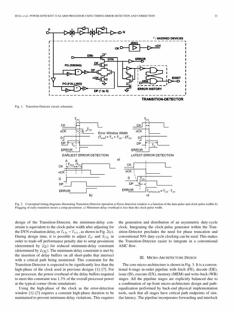
Fig. 1 shows the design of the Transition-Detector augmentedto a rising-edge triggered master-slave flip-flop. We use a similardesign of the Transition-Detector to monitor critical memoryaccess paths and clock-gating enables. The Transition-Detectorflags late-arriving transitions at the monitored net by generatinga pulse in response to the transition and capturing it within aclock-pulse, generated from the rising-edge of the clock (CK).
The Transition-Detector incorporates two conventionalpulse-generators for both rising and falling transitions on theD input. The pulse-generators use skewed devices sized suchthat the rising transition of the output pulse is favoured overthe falling, thereby generating a wide pulse at the output of thepulse-generator. The width of the data-pulse is determined bythe sizing of the pMOS transistors in the p-skewed inverters

20 IEEE JOURNAL OF SOLID-STATE CIRCUITS, VOL. 46, NO. 1, JANUARY 2011
TABLE ICLASSIFICATION OF VARIATIONS
(with minimum-sized NMOS) and the nMOS transistors inthe n-skewed NAND gates (with minimum-sized PMOS). Thedelay chain on the internal clock network defines an implicitclock pulse that is active when transistors N1 (enabled by CK)and N2 (enabled by nCK, the delayed and inverted versionof CK) are both ON. The data-pulse can be captured whenthe clock-pulse is active by discharging the dynamic node,DYN, thereby flagging the ERROR signal. The ERN signal isgenerated during pipeline recovery initiated in response to theERROR signal being flagged. It resets the Transition-Detectorby precharging the dynamic node, DYN, and enabling it tocapture subsequent timing errors. Thus, DYN is conditionallyprecharged only in the event of a timing error.
An additional RS-latch structure acts as a sticky error history(EHIST) bit that is set whenever an error occurs. The EHISTinformation is extremely useful for offline diagnostics sincereading out the EHIST information allows precise identificationof each Transition-Detector that triggered over the course of atest. The EHIST bit adds an additional 10% area and leakageoverhead to the Transition-Detector. However, the diagnosticcapability of the EHIST bit is required only during the initialdevelopment phase of a design and can be excluded in a pro-duction design.
Fig. 2 shows the conceptual timing diagrams that explain theprinciple of operation of the Transition-Detector. The implicitclock-pulse is active in the interval between the rising edge ofCK and the falling edge of nCK. As mentioned previously, thewidth of the clock-pulse and the width of the data-pulse
are determined by the internal clock-network delay and thesizing of the pulse generators, respectively. Fig. 2(a) shows theeffective error-detection window. The error-detection windowbegins (ends) when the trailing (leading) edge of the data-pulseoverlaps with the leading (trailing) edge of the clock-pulse forduration greater than the minimum overlap (Tov) required forevaluating the dynamic node, DYN. Thus, the total error-detec-tion window width is the aggregate ofthe data-pulse and the clock-pulse widths after adjusting for theminimum overlap required at the leading and the trailing edges.
The detection-window is fixed after design and needs to beadequate such that the delay-impact due to fast-moving phe-nomena can be detected and recovered from. Typically, the de-vice widths in the pulse-generators are sized so as to minimizethe total power overhead of detection while allowing sufficient
detection-window width. From simulation results, on the pro-cessor described in this paper, the generation of the error-de-tection window resulted in the total power overhead due to theTransition-Detectors to be 5.7% of the overall processor powerat the typical corner (TT/1.0V/85C).
In order that metastability in the main flip-flop is suitably de-tected and flagged, the error-detection window needs to coverthe setup window of the main flip-flop with sufficient margin,across PVT corners. Setup coverage is ensured by appropriatelysizing the pulse-generators for a sufficiently wide data-pulse.Due to the added margin on the setup window, early transi-tions on the D input are now flagged as errors, even beforethey cause actual setup violations and state-upsets in the mainflip-flop. This difference between the onset of the setup windowand error-detection window, shown in Fig. 2(b), is a measureof the setup pessimism that is inherent in this design.This pessimism was measured on silicon to be ofthe cycle time for 1 GHz operation, compared to the actual fre-quency where incorrect state starts to be latched.
“Q” can become metastable when the input “D” transitions inthe setup window (the onset of which is marked by point B inFig. 2(b)). However, this is reliably detected and flagged by theTransition-Detector since the error-detection window subsumesthe setup window by design. The ERROR output of the Transi-tion-Detector can become metastable due to a partial dischargeof the node, DYN, at the onset of the error-detection window(marked by point A in Fig. 2(b)). However, since this occursbefore the main flip-flop setup window, the output “Q” is guar-anteed to transition to its correct state without any impact on itstiming. Thus, metastability at the ERROR signal does not causestate corruption within the pipeline.
Although extremely unlikely, it is possible that a metastableERROR output can potentially propagate to the pipeline re-covery circuit. We address this in the conventional manner byensuring that the ERROR signals are eventually double-latchedwithin the pipeline before being processed by the recoverycircuit. This is subsequently discussed in greater detail inSection III along with the micro-architectural description of thedesign.
The Transition-Detector imposes a minimum-delay con-straint to prevent early transitions from being flagged as errors.The portion of the error-detection window that exists after theclock-edge determines the minimum-delay constraint. For this
BULL et al.: POWER-EFFICIENT 32 bit ARM PROCESSOR USING TIMING-ERROR DETECTION AND CORRECTION 21
Fig. 1. Transition-Detector circuit schematic.
Fig. 2. Conceptual timing diagrams illustrating Transition-Detector operation a) Error-detection window is a function of the data-pulse and clock-pulse widths b)Flagging of early transition incurs a setup pessimism. c) Minimum-delay overhead is less than the clock-pulse width.
design of the Transition-Detector, the minimum-delay con-straint is equivalent to the clock-pulse width after adjusting forthe DYN evaluation delay, or , as shown in Fig. 2(c).During design time, it is possible to adjust and inorder to trade-off performance penalty due to setup pessimism(determined by ) for reduced minimum-delay constraint(determined by ). The minimum-delay constraint is met bythe insertion of delay buffers on all short-paths that intersectwith a critical path being monitored. This constraint for theTransition-Detector is expected to be significantly less than thehigh-phase of the clock used in previous designs [1]–[7]. Forour processor, the power overhead of the delay buffers requiredto meet this constraint was 1.3% of the overall processor powerat the typical corner (from simulation).
Using the high-phase of the clock as the error-detectionwindow [1]–[7] requires a constant high-phase duration to bemaintained to prevent minimum-delay violations. This requires
the generation and distribution of an asymmetric duty-cycleclock. Integrating the clock-pulse generator within the Tran-sition-Detector precludes the need for phase truncation andconventional 50% duty-cycle clocking can be used. This makesthe Transition-Detector easier to integrate in a conventionalASIC flow.
III. MICRO-ARCHITECTURE DESIGN
The core micro-architecture is shown in Fig. 3. It is a conven-tional 6-stage in-order pipeline with fetch (FE), decode (DE),issue (IS), execute (EX), memory (MEM) and write-back (WB)stages. All the pipeline stages are explicitly balanced due toa combination of up-front micro-architecture design and path-equalization performed by back-end physical implementationtools, such that all stages have critical path endpoints of sim-ilar latency. The pipeline incorporates forwarding and interlock

22 IEEE JOURNAL OF SOLID-STATE CIRCUITS, VOL. 46, NO. 1, JANUARY 2011
Fig. 3. Pipeline diagram of the ARM-based processor showing error-detecting Transition-Detectors and recovery control.
logic resulting in additional fanin to both dataplane and controlpaths.
Tightly-Coupled instruction and data memories (IRAM andDRAM), 2 KB each, hold 512 instruction and data words,respectively. As in commercial ARM microprocessor designs,the instruction and data-memory access paths are critical.Transition-detectors monitor the RAM interfaces and flagtiming violations at the address and the chip-select pins duringcritical loads or instruction fetches. DRAM write accesses arerequired to be non-critical and this is guaranteed by suitablybuffering store data, which eventually gets written into memoryafter Razor validation. Pipeline registers are aggressivelyclock-gated for low-power operation. Integrated Clock-gatingCells (ICGs) with critical enables are also augmented withTransition-Detectors.
The ERROR signals of individual stages are OR-ed togetherand registered to generate the stage error signal. This is thenOR-ed with the ERROR signals from the subsequent stagesand so on. The composite pipeline ERROR signal (Fig. 3) isdouble-latched to mitigate against potential metastability. Con-sequently, all instruction commits have to be postponed by twoextra stabilization stages, S0 and S1, to budget for this synchro-nization overhead. Forwarding paths from S0 and S1 preventpipeline interlocks and hence there is no Instruction Per Cycle(IPC) degradation due to these extra stages. From simulationsperformed under typical usage conditions, the power overheaddue to S0 and S1 was 2.4% of the total processor power.
When an error is detected, the entire pipeline is flushed andthe next un-committed instruction is replayed. Replay occurs athalf-frequency such that a failing instruction does not incur re-peated timing errors, thereby maintaining forward progress inthe pipeline. Micro-architectural replay is a conventional tech-nique that often already exists in high-performance pipelines
to support speculative execution such as out-of-order executionand branch-prediction. Therefore, it is possible to extend pre-ex-isting recovery framework to support Razor timing speculation.
IV. CHIP IMPLEMENTATION DETAILS
Fig. 4 shows the die photograph of the processor. The pro-cessor implementation details are provided in Table II. The de-sign is fabricated in UMC65SP [15] high-performance processwith 1 V nominal supply voltage and 1.1 V as the overdrivelimit. The STA sign-off frequency was 724 MHz measured atthe worst-case corner (SS/0.9 V/125 C) where margins are bud-geted for 10% voltage droop, slow silicon and temperature ef-fects. We tested and measured 87 die from split-lots silicon with30 samples from the fast (FF) lot, 37 from the typical (TT) and20 samples from the slow (SS) lots, respectively. The proto-type Razor processor is hosted on an ARM CPU sub-systemas a memory-mapped peripheral. The ARM CPU is used as atest-harness for downloading code into the instruction memorythrough an APB [26] bus interconnect. The execution outputfrom the general-purpose Register File (Fig. 3) and the DataMemory (DRAM) is then read-out at the end of every test andcompared with a golden result set for correctness. The processorimplements error rate driven dynamic frequency and voltagecontrol (described in Sections V-A and V-B).
Out of a total of 2976 registers in the design, the top 503most critical registers were augmented with a Transition-De-tector for timing-error detection. This represents approximately17% of the total flip-flops in the design. There are 149 ICG cellsin the design, of which 27 have Transition-Detector protection.The Address and the Chip-Select pins of both the instructionand data memories are monitored using Transition-Detectors.In total, the design incorporates 550 Transition-Detectors. Thetiming-critical endpoints are chosen after timing analysis on a
BULL et al.: POWER-EFFICIENT 32 bit ARM PROCESSOR USING TIMING-ERROR DETECTION AND CORRECTION 23
Fig. 4. Die photograph of the ARM-based Razor processor.
TABLE IIPROCESSOR IMPLEMENTATION DETAILS
placed-and-routed design at the slow corner. After identifyingthe critical path endpoints, the netlist is again taken through theimplementation flow. The final design is then verified at mul-tiple PVT corners to ensure that critical endpoints are alwaysprotected by Transition-Detectors across all corners.
A critical concern during implementation is that the designflow does not result in additional critical endpoints. Otherwise,the timing perturbation due to the incremental insertion of Tran-sition-Detectors may lead to more timing endpoints to becomecritical, thus impacting design closure. We avoid multiple im-plementation iterations by imposing extra timing constraints onthe non-critical endpoints during logic optimization and place-and-route. This ensures that the original list of critical paths ispreserved and design closure is achieved.
Table II shows the total power and area overhead of Razorerror detection and correction circuitry. From simulation resultsat the typical corner (TT/1 V/85 C), the total overhead of the550 Transition-Detectors from simulation results was 5.7% with1.3% overhead due to the delay buffers required to meet theminimum-delay constraint. The stabilization stages (S0 and S1)
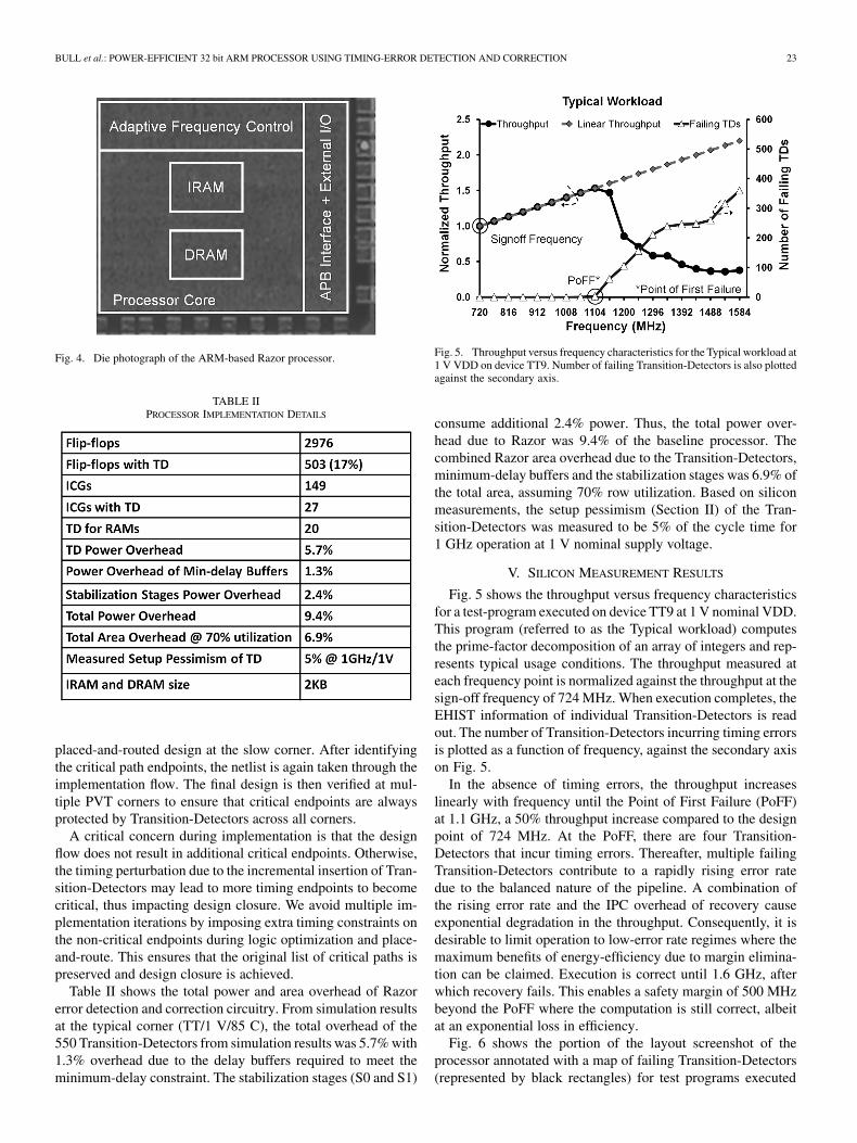
Fig. 5. Throughput versus frequency characteristics for the Typical workload at1 V VDD on device TT9. Number of failing Transition-Detectors is also plottedagainst the secondary axis.
consume additional 2.4% power. Thus, the total power over-head due to Razor was 9.4% of the baseline processor. Thecombined Razor area overhead due to the Transition-Detectors,minimum-delay buffers and the stabilization stages was 6.9% ofthe total area, assuming 70% row utilization. Based on siliconmeasurements, the setup pessimism (Section II) of the Tran-sition-Detectors was measured to be 5% of the cycle time for1 GHz operation at 1 V nominal supply voltage.
V. SILICON MEASUREMENT RESULTS
Fig. 5 shows the throughput versus frequency characteristicsfor a test-program executed on device TT9 at 1 V nominal VDD.This program (referred to as the Typical workload) computesthe prime-factor decomposition of an array of integers and rep-resents typical usage conditions. The throughput measured ateach frequency point is normalized against the throughput at thesign-off frequency of 724 MHz. When execution completes, theEHIST information of individual Transition-Detectors is readout. The number of Transition-Detectors incurring timing errorsis plotted as a function of frequency, against the secondary axison Fig. 5.
In the absence of timing errors, the throughput increaseslinearly with frequency until the Point of First Failure (PoFF)at 1.1 GHz, a 50% throughput increase compared to the designpoint of 724 MHz. At the PoFF, there are four Transition-Detectors that incur timing errors. Thereafter, multiple failingTransition-Detectors contribute to a rapidly rising error ratedue to the balanced nature of the pipeline. A combination ofthe rising error rate and the IPC overhead of recovery causeexponential degradation in the throughput. Consequently, it isdesirable to limit operation to low-error rate regimes where themaximum benefits of energy-efficiency due to margin elimina-tion can be claimed. Execution is correct until 1.6 GHz, afterwhich recovery fails. This enables a safety margin of 500 MHzbeyond the PoFF where the computation is still correct, albeitat an exponential loss in efficiency.
Fig. 6 shows the portion of the layout screenshot of theprocessor annotated with a map of failing Transition-Detectors(represented by black rectangles) for test programs executed
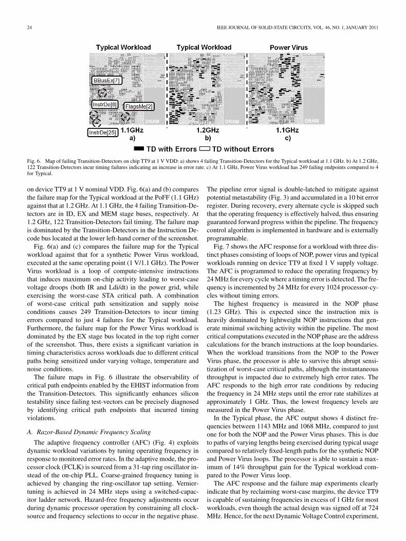
24 IEEE JOURNAL OF SOLID-STATE CIRCUITS, VOL. 46, NO. 1, JANUARY 2011
Fig. 6. Map of failing Transition-Detectors on chip TT9 at 1 V VDD: a) shows 4 failing Transition-Detectors for the Typical workload at 1.1 GHz. b) At 1.2 GHz,122 Transition-Detectors incur timing failures indicating an increase in error rate. c) At 1.1 GHz, Power Virus workload has 249 failing endpoints compared to 4for Typical.
on device TT9 at 1 V nominal VDD. Fig. 6(a) and (b) comparesthe failure map for the Typical workload at the PoFF (1.1 GHz)against that at 1.2 GHz. At 1.1 GHz, the 4 failing Transition-De-tectors are in ID, EX and MEM stage buses, respectively. At1.2 GHz, 122 Transition-Detectors fail timing. The failure mapis dominated by the Transition-Detectors in the Instruction De-code bus located at the lower left-hand corner of the screenshot.
Fig. 6(a) and (c) compares the failure map for the Typicalworkload against that for a synthetic Power Virus workload,executed at the same operating point (1 V/1.1 GHz). The PowerVirus workload is a loop of compute-intensive instructionsthat induces maximum on-chip activity leading to worst-casevoltage droops (both IR and Ldi/dt) in the power grid, whileexercising the worst-case STA critical path. A combinationof worst-case critical path sensitization and supply noiseconditions causes 249 Transition-Detectors to incur timingerrors compared to just 4 failures for the Typical workload.Furthermore, the failure map for the Power Virus workload isdominated by the EX stage bus located in the top right cornerof the screenshot. Thus, there exists a significant variation intiming characteristics across workloads due to different criticalpaths being sensitized under varying voltage, temperature andnoise conditions.
The failure maps in Fig. 6 illustrate the observability ofcritical path endpoints enabled by the EHIST information fromthe Transition-Detectors. This significantly enhances silicontestability since failing test-vectors can be precisely diagnosedby identifying critical path endpoints that incurred timingviolations.
A. Razor-Based Dynamic Frequency Scaling
The adaptive frequency controller (AFC) (Fig. 4) exploitsdynamic workload variations by tuning operating frequency inresponse to monitored error rates. In the adaptive mode, the pro-cessor clock (FCLK) is sourced from a 31-tap ring oscillator in-stead of the on-chip PLL. Coarse-grained frequency tuning isachieved by changing the ring-oscillator tap setting. Vernier-tuning is achieved in 24 MHz steps using a switched-capac-itor ladder network. Hazard-free frequency adjustments occurduring dynamic processor operation by constraining all clock-source and frequency selections to occur in the negative phase.
The pipeline error signal is double-latched to mitigate againstpotential metastability (Fig. 3) and accumulated in a 10 bit errorregister. During recovery, every alternate cycle is skipped suchthat the operating frequency is effectively halved, thus ensuringguaranteed forward progress within the pipeline. The frequencycontrol algorithm is implemented in hardware and is externallyprogrammable.
Fig. 7 shows the AFC response for a workload with three dis-tinct phases consisting of loops of NOP, power virus and typicalworkloads running on device TT9 at fixed 1 V supply voltage.The AFC is programmed to reduce the operating frequency by24 MHz for every cycle where a timing error is detected. The fre-quency is incremented by 24 MHz for every 1024 processor-cy-cles without timing errors.
The highest frequency is measured in the NOP phase(1.23 GHz). This is expected since the instruction mix isheavily dominated by lightweight NOP instructions that gen-erate minimal switching activity within the pipeline. The mostcritical computations executed in the NOP phase are the addresscalculations for the branch instructions at the loop boundaries.When the workload transitions from the NOP to the PowerVirus phase, the processor is able to survive this abrupt sensi-tization of worst-case critical paths, although the instantaneousthroughput is impacted due to extremely high error rates. TheAFC responds to the high error rate conditions by reducingthe frequency in 24 MHz steps until the error rate stabilizes atapproximately 1 GHz. Thus, the lowest frequency levels aremeasured in the Power Virus phase.
In the Typical phase, the AFC output shows 4 distinct fre-quencies between 1143 MHz and 1068 MHz, compared to justone for both the NOP and the Power Virus phases. This is dueto paths of varying lengths being exercised during typical usagecompared to relatively fixed-length paths for the synthetic NOPand Power Virus loops. The processor is able to sustain a max-imum of 14% throughput gain for the Typical workload com-pared to the Power Virus loop.
The AFC response and the failure map experiments clearlyindicate that by reclaiming worst-case margins, the device TT9is capable of sustaining frequencies in excess of 1 GHz for mostworkloads, even though the actual design was signed off at 724MHz. Hence, for the next Dynamic Voltage Control experiment,

BULL et al.: POWER-EFFICIENT 32 bit ARM PROCESSOR USING TIMING-ERROR DETECTION AND CORRECTION 25
Fig. 7. Dynamic Frequency Scaling: AFC response for a 3-phase workload consisting of the NOP, Power Virus and Typical workloads at 1 V VDD. Frequency isincreased or reduced in 24 MHz steps.
Fig. 8. Architecture of the closed-loop Razor voltage controller: The control algorithm is implemented in software running on an ARM1176. The supply voltageis set by programming an external regulator using a DAC.
we keep the frequency fixed at 1 GHz and vary the voltage asdictated by the error rates.
B. Razor-Based Dynamic Voltage Scaling
Fig. 8 shows the architecture of the closed-loop controller im-plemented for dynamic voltage management based on measurederror rates. The control algorithm is implemented in software onthe ARM CPU that hosts the Razor processor sub-system. Thevoltage control decision is based upon the accumulated value of100 samples of the on-chip error register, accessed through theAPB bus interface. The supply voltage is adjusted by program-ming an external DC-DC regulator. The DC-DC regulator cansource 800 mA current that is sufficient for the requirements ofthe Razor processor with maximum current consumption lessthan 150 mA. The response latency of the voltage control loopis measured to be 55 us.
The voltage controller response on device TT9 is shown inFig. 9, for a three-phase program with loops of the NOP, PowerVirus and Typical workloads, running at fixed 1 GHz frequency.The error rate for device TT9 is plotted against the secondaryaxis. The error rate is initially zero in the NOP phase since thesupply voltage is higher than the PoFF for the relatively light-weight NOP instructions. The controller responds to the zeroerror rate by reducing the supply voltage to 0.92 V for deviceTT9, where infrequent timing errors occur. During the tran-sition from the NOP to the Power Virus phase, the processor
experiences a surge in the error rate. The controller respondsto the high error rate by increasing the supply voltage in pro-portional increments until the steady-state voltage is attainedat 1.07 V. Conversely, the error rate drops to zero during thetransition from the Power Virus to the Typical workload phase.The steady-state voltage for the Typical workload is achieved at0.96 V.
The controller response for devices SS6 and FF5 are alsoplotted in Fig. 9. Device SS6 is amongst the slowest die out ofthe 87 devices while FF5 is amongst the fastest with maximumstandby leakage. Thus, these devices represent the extremes ofthe distribution of devices. The steady-state voltage measuredfor the NOP, Power Virus and the Typical phases for each de-vice in Fig. 9 is indicative of its native silicon-grade.
The dynamic voltage and frequency scaling experimentsin Sections V-A and V-B illustrate how Razor maximizesthe energy efficiency of the processor by tuning to the mostefficient operating point depending upon specific workloadrequirements. In situ error detection and recovery enables theRazor processor to maintain correct operation in the presenceof fast-changing dynamic variations and worst-case criticalpath sensitization. When dynamic variations persist, the Razorvoltage controller automatically adapts to higher voltage levelsso that low error rates are eventually achieved. In Section VI,we quantify the energy savings obtainable with Razor-enabledvoltage tuning for 1 GHz operation.

26 IEEE JOURNAL OF SOLID-STATE CIRCUITS, VOL. 46, NO. 1, JANUARY 2011
Fig. 9. Impact of process variations on Razor voltage controller response at 1GHz frequency: Slowest device, SS6, requires the highest voltage and vice versafor the fastest device, FF5. SS6 requires 1.17 V for the Power Virus phase.
VI. RAZOR ENERGY SAVINGS
From the Razor voltage controller response in Fig. 9, weobserve that the slowest chip, SS6, requires a minimum voltageof 1.17 V in order to operate the Power Virus workload at1 GHz frequency. For all our samples to operate correctlywithout Razor, sufficient margin is required to guarantee thatthe slowest device (SS6) operates correctly in the worst-case.Assuming Power Virus is the absolute worse-case code, thenat a bare minimum additional margin must be added for tem-perature and safety. For 1 GHz operation, this translates to aworst-case voltage of 1.2 V for 3% margin. Thus, for conven-tional operation without Razor, the minimum required supplyvoltage is 1.2 V such that all die operate correctly at 1 GHz.
Fig. 10 compares the power consumption for Razor-enabledoperation versus conventional operation at 1.2 V when exe-cuting the Typical workload at 1 GHz frequency for each ofthe three devices (FF5, SS6 and TT9). For the 1.2 V operation,leakage power is a significant contributor to the total power forthe fastest device, FF5 (approximately 50%). The slowest de-vice SS6 consumes the least power at 1.2 V due to low leakage.Even though the SS6 dynamic power is higher than that forFF5, the higher contribution of leakage causes FF5 to be themaximum power outlier for the entire distribution of devices.
With Razor-enabled voltage tuning, all devices operate atthe PoFF for the Typical workload. The lower PoFF for FF5(0.92 V) compared to that for SS6 (1.07 V) compensates for itshigher leakage, leading to SS6 becoming the power outlier forthe distribution. The maximum power consumption for Typicalworkload, considering all 87 devices, reduces from 100 mWfor the baseline 1.2 V operation to 48 mW for operation withRazor. This represents a net 52% power saving at 1 GHzoperation. On a per chip basis, power consumption on TT9reduces from 71 mW at 1.2 V to 40.5 mW using Razor, a net43% power saving due to Razor.
Fig. 10 compares Razor with a hypothetical, best-in-classadaptive technique. Adaptive techniques can be static wherethe supply voltage or the body bias is calibrated, marginedand programmed on the tester [19]–[24]. Dynamic adaptivetechniques [9]–[12], [16]–[18] rely on process and temperature
monitors to scale processor supply voltage according to pre-vailing PVT conditions at runtime. Due to adaptation latency,such techniques cannot respond in time to fast-changing voltagedroops that manifest during abrupt processor activity changes(Fig. 9). At the minimum, margining is required to account forthis latency as well as for measurement uncertainties inherentin the monitoring circuits. For our experiment, we assumea dynamic adaptive loop where voltage scaling is limited tothe Power Virus voltage. Scaling voltage below this level canpotentially cause incorrect execution if the processor undergoesa transition to the Power Virus workload. An additional 3%margin is added to account for measurement uncertainty.
Fig. 10 shows the power consumed for the Typical workloadby the devices SS6, FF5 and TT9 using such a hypotheticalbest-case adaptive technique. This is a best-case comparison ofthe adaptive approach against Razor since only the minimumrequired margins are accounted for. Typically, margins for localtemperature fluctuations and ageing effects are also added whichwill then lead to higher power consumption for the adaptiveapproach. The device TT9 requires 1.1 V using the best-caseadaptive tuning and consumes 58.7 mW for the Typical work-load. With Razor, TT9 consumes 40.5 mW that represents a 30%power saving due to Razor compared to the adaptive approach.The worst-case power, due to SS6, reduces by 25% using Razor.
Fig. 11 shows the power distribution for the 87 devices withRazor versus operation at 1.2 V and the best-case adaptive tech-nique. The power distribution at constant 1.2 V VDD is dom-inated by the fast and leaky devices and therefore has largespread (37 mW). In contrast, the power distribution with Razorhas a significantly narrower spread (10 mW) due to the equal-ization effect of a higher PoFF for the slower devices compen-sating for the higher leakage on the faster devices. The mean ofthe power distribution improves by 30 mW using Razor, a net40% improvement over 1.2 V operation. Compared to best-caseadaptive tuning, the mean of the distribution shifts by 14 mW(or 24%) when using Razor.
Sustained operation beyond the process overdrive limit of1.1 V can have potential long-term gate-oxide reliability [14]and accelerated wear-out implications [13]. In addition, exces-sive overdrive exacerbates short-channel effects such as DrainInduced Barrier Lowering (DIBL) [24] leading to exponentialincrease in leakage, especially on the fast devices. From reli-ability and leakage considerations, it is desirable to limit thevoltage overdrive to the process limit of 1.1 V.
SS6 requires at least 1.17 V when executing the worst-casePower Virus workload at 1 GHz. Hence, limiting the long-termoverdrive operation to 1.1 V would necessarily require SS6 tobe discarded when operating without Razor at 1 GHz frequency.Consequently, without Razor, operation at 1.1 V most certainlyincurs a parametric yield loss for a frequency target of 1 GHzdue to discarding the slow devices. In Section VII, we analyzethe impact on parametric yield at 1 GHz when the maximumvoltage for sustained, long-term operation is limited to 1.1 V.
VII. PARAMETRIC YIELD IMPROVEMENT USING RAZOR
Any yield improvement technique cannot be quantitativelydemonstrated with a small number of samples, however we canstill illustrate the principle of how Razor can be used to improve

BULL et al.: POWER-EFFICIENT 32 bit ARM PROCESSOR USING TIMING-ERROR DETECTION AND CORRECTION 27
Fig. 10. Power consumption on devices FF5, TT9 and SS6: Razor is compared against constant 1.2 V VDD and best-case Adaptive-tuning. Razor enables 52%power saving overall compared to constant 1.2 V operation. Razor enables 30% power saving compared to best-case adaptive tuning for device TT9 and 43%saving compared to1.2 V operation.
Fig. 11. Power distribution at the worst-case (WC) 1.2 V constant voltage operation versus Razor. Razor improves both the m and the s of the distribution.
the parametric yield for a distribution of devices. Functionaldevices are required to meet a targeted frequency specification(Fmax) under a given power budget (Pmax), before they can beshipped. In the following, we compare the parametric yield ob-tained using Razor versus that with conventional overdrive op-eration at constant 1.1 V VDD and an Adaptive Voltage Scaling(AVS) approach based on an on-chip Ring Oscillator serving asa process monitor. We have chosen the parametric yield targetsof 1 GHz frequency under 65 mW power consumption for typ-ical usage conditions.
A. Parametric Yield With Constant 1.1 V Overdrive
The scatter plot in Fig. 12 shows the total power consumption(dynamic and leakage) as a function of silicon-grade for all de-vices when executing the Typical workload at the 1.1 V/1 GHzoperating point, without Razor. Operation without Razor re-quires margins for the worst-case. Assuming Power Virus to bethe worst-case workload, we obtain the maximum frequency ofoperation for each die by measuring the Point of First Failure(PoFF) frequency (with 3% margin added for safety), when ex-ecuting the Power Virus workload at 1.1 V VDD. Thus, the mea-
Fig. 12. Power at 1 GHz for Typical workload versus silicon-grade measuredby highest frequency for correct operation without Razor at 1.1 V constant VDD.Measurements obtained on 87 die from split lots. Yield window is shown forfrequency target (Fmax) of 1 GHz and power target (Pmax) of 65 mW.
sured PoFF for the worst-case Power Virus workload representsa margined frequency point under typical usage conditions.

28 IEEE JOURNAL OF SOLID-STATE CIRCUITS, VOL. 46, NO. 1, JANUARY 2011
The device, FF5, sustains the highest frequency (1127 MHz)for worst-case operation and consumes maximum power due tohigh leakage. Devices SS6 and TT13 from the slow and the typ-ical lots respectively, are the slowest devices from our test sam-ples and operate the Power Virus workload at 890 MHz. Thus,the devices follow an expected exponential trend with the fastdevices with high leakage dominating the total power consump-tion compared to the slower devices.
Fig. 12 shows the parametric yield targets of frequency andpower, labeled as “Fmax” and “Pmax” respectively. Out of 87devices, there are 7 devices that exceed the 65 mW power cri-teria and 44 devices that fail the 1 GHz frequency criteria. Thus,there are 36 yielding devices (or 41% yield) out of a total of 87.
B. Parametric Yield With Adaptive Voltage Scaling (AVS)
AVS techniques [9]–[12], [16]–[21] individually tune thesupply voltage of devices according to their native speed-grade,based on delay measurements using on-chip process monitors.Per-device tuning compensates for inter-die process variations.However, extra margins are still required for fast-moving tran-sients that are impossible to respond to in time. Such transientscan trigger during abrupt processor transition from low-activityand non-critical operations to compute-intensive, heavyweightinstructions. Consequently, for safe operation, AVS is requiredto be limited to a sufficiently margined point. We derive thissafe operating limit based on the failure point for the PowerVirus workload with added margin for safety (3%). In theabsence of dynamic detection and correction of errors, the AVStechnique cannot operate below this voltage due to potentialrisk of incorrect execution.
Our AVS measurements use an on-chip Ring Oscillator for es-timating the worst-case processor delay. We obtain a statisticalcorrelation function using a linear-fit model that relates the mea-sured Ring Oscillator frequency at 1 V VDD to the minimumsafe voltage requirement at 1 GHz. Due to the limited numberof test devices, we measure the correlation function using datafrom every die. In the general case, a small number of samplesfrom different global corners of the process distribution couldbe used as a training set to generate the correlation function forthe entire distribution of devices.
In our measurements, we add margins to the linear-fitmodel only to account for possible under-estimation of thedevice voltage from the measured Ring Oscillator frequency.Discounting margins for temperature and ageing allows anoptimistic comparison of AVS against Razor. Fig. 13 showsthe scatter plot of the PoFF voltage for Power Virus workloadversus the Ring-Oscillator frequency measured at 1 V for diefrom the fast (FF), slow (SS) and typical (TT) lots, respectively.It can be observed that the Ring Oscillator frequency is stronglycorrelated with the minimum voltage requirement for each die.The statistical correlation function for both data sets is com-puted to be 95.3% for the entire training set of devices. Whenmeasured across separate lots, this correlation is computed tobe 86.2% for the FF lot, 85.1% for the SS lot and 89.1% forthe TT lot, respectively. Due to the high correlation measuredacross global process corners, the Ring Oscillator frequencycan be used to set the supply voltage for individual devices.
Fig. 13. Scatter-plot of the Power Virus PoFF (with 3% margin for safety) at1 GHz versus measured Ring Oscillator frequency at 1.0 V: Ring-Oscillator fre-quency shows significant correlation (95%) with the minimum safe voltage, thusshowing accurate tracking across global process corners. Extra margin added forvoltage underestimation (36 mV).
Fig. 14. Comparison of Ring-Oscillator based AVS with constant 1.1 V oper-ation: Scatter-plot of power at 1 GHz running typical code for both techniquesis shown as a function of silicon-grade. The maximum power reduces with AVSdue to voltage scaling on fast chips. However, power increases on slow chipsdue to VDD exceeding 1.1 V limit leading to the U-shaped trend.
Fig. 13 shows the margining methodology for the Ring Os-cillator based AVS. The device TT3 shows the maximum devi-ation from the linear-fit model, leading to a voltage underesti-mation of 36 mV. Consequently, this voltage difference has tobe added as extra margin to the model to guarantee that the es-timated voltage is always greater than the minimum voltage re-quired for safe operation. This margin (36 mV) represents 3.2%of the nominal voltage overdrive of 1.1 V.
The scatter plot of Fig. 14 shows the power consumptionof each die using the margined AVS model in Fig. 13 plottedagainst its native silicon-grade (maximum worst-case fre-quency of operation with 3% margin). The U-shaped trend ofthe scatter plot is a consequence of the power reduction on thefaster devices due to lower voltage operation and vice versa forthe slower devices. The maximum power consumption reducesfrom 76 mW at constant 1.1 V operation to 68 mW using AVS,a net 11% reduction in total power.
The voltage on the slow devices using AVS exceeds the 1.1 Voverdrive limit. In addition, the extra 36 mV margin for voltageunderestimation causes some of the typical devices to exceed

BULL et al.: POWER-EFFICIENT 32 bit ARM PROCESSOR USING TIMING-ERROR DETECTION AND CORRECTION 29
Fig. 15. Power versus silicon-grade scatter plot for AVS: Maximum supplyvoltage is limited to 1.1 V VDD when the AVS voltage exceeds this limit on theslow die. VDD tuning on the fast-die reduces the max power for the distributionwhich improves the power yield. However, frequency yield is unchanged.
the 1.1 V limit as well. Due to wearout and reliability concerns,we limit the maximum voltage to the process overdrive limitof 1.1 V for sustained, long-term operation. As a consequence,devices incapable of sustaining correct operation at 1.1 V arenow discarded, leading to yield loss.
Fig. 15 shows the power versus silicon-grade scatter plotwhere maximum VDD is limited to 1.1 V. AVS leads to lowerpower consumption on the fast devices with the maximumpower outlier at 68 mW. Excluding the 2 devices violating themaximum power constraint and the 44 devices fail the 1-GHzfrequency constraint, there are now 41 yielding devices out of87, or 47% yield.
C. Parametric Yield With Razor
Fig. 16 shows the power versus silicon-grade scatter plot forRazor-enabled operation on 87 devices executing the Typicalworkload at 1 GHz frequency. The silicon-grade is again repre-sented by the maximum frequency of operation, sustainable atconstant 1.1 V VDD. Due to the elimination of worst-case mar-gins using Razor, each device operates at a higher frequencywhen executing the Typical workload compared to the worst-case Power Virus workload. Therefore, the entire scatter plotshifts to higher frequency values. The slowest device, SS6, canexecute the Typical workload at near zero error rate conditions at1015 MHz at 1.1 V VDD, thus exceeding the 1 GHz frequencytarget. The highest PoFF for the Typical workload is measuredto be 1397 MHz on device, FF76.
The maximum power outlier when using Razor is measuredto be 48 mW which represents a 26% saving over the powertarget of 65 mW and a net 37% saving over the worst-case power(76 mW) at constant 1.1 V operation. Thus, all devices simul-taneously meet both the power and frequency targets and 100%yield is achieved. The yield obtained for the 1 GHz/65 mW para-metric targets using constant 1.1 V operation, AVS and Razorapproaches is summarized in Table III.
A key observation here is that in case of Razor, the slowestdevice SS6 executes most workloads below the process limit
Fig. 16. Parametric yield with Razor compared against that with constant 1.1 VVDD operation. Frequency uplift through margin reclamation on slow devicesand voltage scaling to PoFF for fast devices enables 100% yield through Razor.
TABLE IIISUMMARY OF YIELD OBTAINED USING THE 3 DIFFERENT TECHNIQUES:
CONSTANT 1.1 V OVERDRIVE, AVS AND RAZOR-TUNING FOR 87 TOTAL DIE
of 1.1 V. Thus, for long-term operation the supply voltage iskept below 1.1 V for all devices, except for extremely rareuse cases equivalent to the pathological worst-case PowerVirus code. This is in contrast with the AVS approach whereoperation beyond 1.1 V is sustained on a long-term basis forthe slower devices. Furthermore, safety margins and correlationuncertainties cause more devices to require greater than 1.1 Vsupply in the AVS approach compared to Razor.
For applications where the peak power consumption is a fun-damental constraint, packaging and thermal limitations can im-pose absolute restrictions on the supply voltage from exceedingthe 1.1 V VDD limit, even for the Power Virus workload. Fromour measurements, there are 22 devices out of 87 that requiresupply voltage in excess of 1.1 V for the Power Virus workloadwith Razor-enabled operation. Discarding these devices leadsto 65 yielding devices (or 75% yield) when strict limits on themaximum voltage of operation are applied.
VIII. SUMMARY AND CONCLUSION
In this paper, we presented the design of an ARM-basedmicroprocessor that uses Razor for energy-efficient operationthrough the elimination of timing margins. With Razor-basedvoltage tuning, we achieved 52% energy savings at 1 GHzoperation on a distribution of 87 devices from split-lots. Wepresented the design of a Transition-Detector with significantlyreduced minimum-delay impact. The Transition-Detector relieson locally generated clock and data-pulses and can operateusing conventional 50% duty-cycle clocking. Thus, it can beeasily integrated into a conventional ASIC design flow.

30 IEEE JOURNAL OF SOLID-STATE CIRCUITS, VOL. 46, NO. 1, JANUARY 2011
We demonstrated the operation of dynamic frequency andvoltage controllers that enable runtime adaptation to PVT varia-tions and tolerance of fast transients through Razor error detec-tion and recovery. The dynamic frequency controller was im-plemented in hardware on-chip and relies on a Ring-Oscillatorclock-source to adjust frequency according to monitored errorrates. The voltage controller was implemented in software run-ning on a separate ARM processor that samples the error reg-ister through an APB bus interface and adjusts the voltage byprogramming an external voltage regulator.
Finally, we demonstrated the potential for parametric yieldimprovement using Razor. By trading margins for higherfrequency on the slow devices and lower power on the fast de-vices, Razor-tuning enables more devices to meet the dual-sidedparametric yield constraints of frequency and power. Furtherresearch is required to develop suitable manufacturing testmethodologies before Razor can be deployed in the field. Asprocess technology scales to ultra-small geometries, Razormitigates the impact of rising variations by simultaneouslyenabling higher performance at lower power consumption.
ACKNOWLEDGMENT
The authors would like to thank staff at United Microelec-tronics Corporation (UMC) for providing, integrating, and fab-ricating the silicon, as well as D. Flynn, S. Idgunji, and J. Biggsat ARM for developing the “Ulterior” technology demonstratorchip that hosts the Razor subsystem.
REFERENCES
[1] S. Das et al., “A self-tuning DVS processor using delay-error detectionand correction,” IEEE J. Solid-State Circuits, pp. 792–804, Apr. 2006.
[2] D. Ernst et al., “Razor: A low-power pipeline based on circuit-leveltiming speculation,” in Proc. IEEE Micro Int. Symp. Microarchitecture,Dec. 2003, pp. 7–18.
[3] D. Blaauw et al., “RazorII: in situ error detection and correction forPVT and SER tolerance,” in IEEE ISSCC Dig. Tech. Papers, Feb. 2008,pp. 400–401.
[4] S. Das et al., “Razor II: in situ error detection and correction for PVTand SER tolerance,” IEEE J. Solid-State Circuits, pp. 32–48, Jan. 2009.
[5] K. Bowman et al., “Energy-Efficient and metastability-immune timing-error detection and instruction replay-based recovery circuits for dy-namic variation tolerance,” IEEE J. Solid-State Circuits, pp. 49–63,Jan. 2009.
[6] J. Tschanz et al., “A 45 nm resilient and adaptive microprocessor corefor dynamic variation tolerance,” in IEEE ISSCC Dig. Tech. Papers,Feb. 2010, pp. 282–283.
[7] J. Tschanz et al., “Tunable replica circuits and adaptive voltage-fre-quency techniques for dynamic voltage, temperature, and aging varia-tion tolerance,” in IEEE Symp. VLSI Circuits Dig., Jun. 2009.
[8] D. Bull et al., “A power-efficient ARM ISA processor using timing-error detection and correction for timing-error tolerance and adaptationto PVT variations,” in IEEE ISSCC Dig. Tech. Papers, Feb. 2010, pp.284–285.
[9] A. Drake et al., “A distributed critical path timing monitor for a 65nm high-performance microprocessor,” IEEE ISSCC Dig. Tech. Pa-pers, 2007.
[10] J. Tschanz et al., “Adaptive frequency and biasing techniques for tol-erance to dynamic temperature-voltage variations and aging,” in IEEEISSCC Dig. Tech. Papers, Feb. 2007, pp. 292–293.
[11] M. Nakai et al., “Dynamic voltage and frequency management for alow power embedded microprocessor,” IEEE J. Solid-State Circuits,pp. 28–35, Jan. 2005.
[12] K. Nowka, “A 32-bit PowerPC system-on-a-chip with support for dy-namic voltage scaling and dynamic frequency scaling,” IEEE J. Solid-State Circuits, Nov. 2002.
[13] S. Rangan, N. Mielke, and E. Yeh, “Universal recovery behavior ofnegative bias temperature instability,” in IEEE Int. Electron DevicesMeeting Dig., Dec. 2003, pp. 341–341.
[14] A. M. Yassine et al., “Time dependent breakdown of ultrathin gateoxide,” IEEE Trans. Electron Devices, pp. 1416–1420, Jul. 2000.
[15] UMC United Microelectronics Corporation [Online]. Available: http://www.umc.com/
[16] T. Fischer et al., “A 90-nm variable frequency clock system for apower-managed itanium architecture processor,” IEEE J. Solid-StateCircuits, pp. 218–228, Jan. 2006.
[17] R. McGowen et al., “Power and temperature control on a 90-nm ita-nium family processor,” IEEE J. Solid-State Circuits, pp. 229–237, Jan.2006.
[18] N. James et al., “Comparison of split- versus connected-core suppliesin the POWER6TM microprocessor,” in IEEE ISSCC Dig. Tech. Pa-pers, Feb. 2007, pp. 297–298.
[19] J. Kao, M. Miyazaki, and A. R. Chandrakasan, “A 175-mV multiply-accumulate unit using an adaptive supply voltage and body bias archi-tecture,” IEEE J. Solid-State Circuits, pp. 1545–1554, Nov. 2002.
[20] J. Tschanz et al., “Adaptive body bias for reducing impacts of die-to-dieand within-die parameter variations on microprocessor frequency andleakage,” IEEE J. Solid-State Circuits, pp. 1396–1402, Nov. 2002.
[21] J. Tschanz et al., “Effectiveness of adaptive supply voltage and bodybias for reducing impact of parameter variations in low power andhigh performance microprocessors,” IEEE J. Solid-State Circuits, pp.826–829, May 2003.
[22] G. Gammie et al., “A 45 nm 3.5 G baseband-and-Multimedia appli-cation processor using adaptive body-bias and ultra-low-power tech-niques,” in IEEE ISSCC Dig. Tech. Papers, Feb. 2008, pp. 258–259.
[23] C. Neau and K. Roy, “Optimal body bias selection for leakageimprovement and process compensation over different technologygenerations,” in Proc. Int. Symp. on Low Power Electronic Devices(ISLPED), Aug. 2003, pp. 116–121.
[24] A. Hokazono et al., “Forward body biasing as a bulk-si CMOStechnology scaling strategy,” IEEE Trans. Electron Devices, pp.2657–2664, Oct. 2008.
[25] R. Kaur et al., “Unified subthreshold model for channel-engineeredsub-100-nm advanced MOSFET structures,” IEEE Trans. Electron De-vices, pp. 2475–2486, Sep. 2007.
[26] AMBA APB Bus Specification Reference Manual [Online]. Avail-able: http://arminfo/help/topic/com.arm.doc.ihi0024c/IHI0024C_amba_apb_protocol_v2_0_spec.pdf
David Bull received the B.Sc. degree in computerscience from Royal Holloway College, University ofLondon, U.K., in 1991.
He is a consultant engineer at ARM Ltd., Cam-bridge, U.K. He joined ARM in 1995, and spent nineyears working on various aspects of processor de-velopment including micro-architecture and circuits.He has worked on the ARM9 and ARM11 processorfamilies processor, and was the design lead for theARM926EJ-S. Since 2004 he has focused on re-search into advanced circuit and micro-architectural
techniques, and has led the ARM RAZOR research project.
Shidhartha Das (S’03–M’08) received the B.Techdegree in electrical engineering from the Indian In-stitute of Technology, Bombay, India, in 2002 andthe M.S. and Ph.D. degrees in computer science andengineering from the University of Michigan at AnnArbor in 2005 and 2009.
His research interests include micro-architecturaland circuit techniques for low-power and variability-tolerant digital IC design. Currently, he is a Staff En-gineer working for ARM Ltd., Cambridge, U.K., inthe Research and Development group.

BULL et al.: POWER-EFFICIENT 32 bit ARM PROCESSOR USING TIMING-ERROR DETECTION AND CORRECTION 31
Karthik Shivashankar received the B.E. degree inelectronics and communications from The NationalInstitute of Engineering, Mysore, India, in 2006 andthe M.Sc. degree in microelectronics from Universityof Liverpool, U.K., in 2008.
His research interests include design methodolo-gies for DVFS controller algorithms. Currently, heis working as an Engineer at ARM Ltd., Cambridge,U.K., in the Research and Development group.
Ganesh S. Dasika (S’01) received the B.S.E. degreein computer engineering from the University ofMichigan at Ann Arbor, where he is now a Ph.D.student in the Department of Electrical Engineeringand Computer Science.
His research interests mainly include designingand compilation for power-efficient, domain-specificprocessors. He is a student member of the IEEE.
Krisztian Flautner (S’96–M’01) received the Ph.D.degree in computer science and engineering from theUniversity of Michigan at Ann Arbor, where he iscurrently appointed as a visiting scholar.
He is the Vice President of research and develop-ment at ARM. ARM designs the technology that liesat the heart of advanced digital products with morethan fifteen billion processors deployed. He leads aglobal team which is focused on the understandingand development of technologies relevant to the pro-liferation of the ARM architecture. The group’s activ-
ities cover a wide breadth of areas ranging from circuits, through processor andsystem architectures to tools and software. Key activities are related to high-per-formance computing in energy-constrained environments.
Dr. Flautner is a member of the ACM and the IEEE.
David Blaauw (M’94–SM’07) received the B.S.degree in physics and computer science fromDuke University, Durham, NC, in 1986, the M.S.degree in computer science from the University ofIllinois, Urbana, in 1988, and the Ph.D. degree incomputer science from the University of Chicago atUrbana-Champaign in 1991.
Until 2001, he was with Motorola, Inc., Austin,TX, where he was the Manager with the High Per-formance Design Technology Group. Since 2001, hehas been on the faculty at the University of Michigan,
Ann Arbor, where he is currently a Professor. His work has focused on very largescale integration design with particular emphasis on ultralow power and highperformance design. His current research interests include high-performanceand low-power VLSI circuits, particularly addressing nanometer design issuespertaining to power, performance, and robustness.
Dr. Blaauw was the Technical Program Chair and General Chair for the In-ternational Symposium on Low Power Electronic and Design. He was also theTechnical Program Co-Chair of the ACM/IEEE Design Automation Conferenceand a Member of the International Solid-State Circuits Conference (ISSCC)Technical Program Committee.