Embed Size (px)
Citation preview
Mu
ltip
lexe
r
Oscillator
CS
SCLK
SDI
SDO
DAISY
REFSEL
RST / PD
REFCAP
REFIO
PGA
1 M:
OVP
1 M:
2nd-OrderLPF
ADCDriver
VB0
AIN_0PAIN_0GND OVP
PGA
1 M:
OVP
1 M:
2nd-OrderLPF
ADCDriver
VB1
AIN_1PAIN_1GND OVP
PGA
1 M:
OVP
1 M:
2nd-OrderLPF
ADCDriver
VB2
AIN_2PAIN_2GND OVP
PGA
1 M:
OVP
1 M:
2nd-OrderLPF
ADCDriver
VB3
AIN_3PAIN_3GND OVP
PGA
1 M:
OVP
1 M:
2nd-OrderLPF
ADCDriver
VB4
AIN_4PAIN_4GND OVP
PGA
1 M:
OVP
1 M:
2nd-OrderLPF
ADCDriver
VB5
AIN_5PAIN_5GND OVP
PGA
1 M:
OVP
1 M:
2nd-OrderLPF
ADCDriver
VB6
AIN_6PAIN_6GND OVP
PGA
1 M:
OVP
1 M:
2nd-OrderLPF
ADCDriver
VB7
AIN_7PAIN_7GND OVP
AUX_INAUX_GND
18-BitSAR ADC
Digital Logic and
Interface
4.096-VReference
REFGNDDGNDAGND
DVDDAVDD
Ad
dit
ion
al C
han
nel
s in
AD
S86
98
ADS8698
ADS8694
ALARM
Internal ADC Operating as 16-Bit ADC -0.05
-0.03
-0.01
0.01
0.03
0.05
±40 ±7 26 59 92 125
Gai
n (%
FS
)
Free-Air temperature (oC) C027
----- ± 2.5*VREF ----- � 1.25*VREF ----- � 0.625*VREF ----- + 2.5*VREF -----+1.25*VREF
Product
Folder
Sample &Buy
Technical
Documents
Tools &
Software
Support &Community
ReferenceDesign
ADS8694, ADS8698SBAS686 –JULY 2015
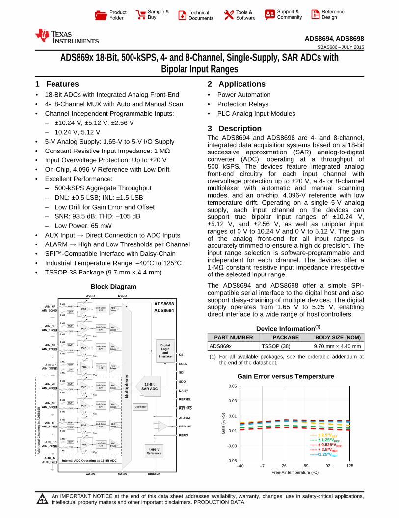
ADS869x 18-Bit, 500-kSPS, 4- and 8-Channel, Single-Supply, SAR ADCs withBipolar Input Ranges
1 Features 2 Applications1• 18-Bit ADCs with Integrated Analog Front-End • Power Automation• 4-, 8-Channel MUX with Auto and Manual Scan • Protection Relays• Channel-Independent Programmable Inputs: • PLC Analog Input Modules
– ±10.24 V, ±5.12 V, ±2.56 V3 Description– 10.24 V, 5.12 VThe ADS8694 and ADS8698 are 4- and 8-channel,• 5-V Analog Supply: 1.65-V to 5-V I/O Supply integrated data acquisition systems based on a 18-bit
• Constant Resistive Input Impedance: 1 MΩ successive approximation (SAR) analog-to-digitalconverter (ADC), operating at a throughput of• Input Overvoltage Protection: Up to ±20 V500 kSPS. The devices feature integrated analog• On-Chip, 4.096-V Reference with Low Drift front-end circuitry for each input channel with
• Excellent Performance: overvoltage protection up to ±20 V, a 4- or 8-channelmultiplexer with automatic and manual scanning– 500-kSPS Aggregate Throughputmodes, and an on-chip, 4.096-V reference with low– DNL: ±0.5 LSB; INL: ±1.5 LSBtemperature drift. Operating on a single 5-V analog
– Low Drift for Gain Error and Offset supply, each input channel on the devices can– SNR: 93.5 dB; THD: –105 dB support true bipolar input ranges of ±10.24 V,
±5.12 V, and ±2.56 V, as well as unipolar input– Low Power: 65 mWranges of 0 V to 10.24 V and 0 V to 5.12 V. The gain• AUX Input → Direct Connection to ADC Inputs of the analog front-end for all input ranges is
• ALARM → High and Low Thresholds per Channel accurately trimmed to ensure a high dc precision. Theinput range selection is software-programmable and• SPI™-Compatible Interface with Daisy-Chainindependent for each channel. The devices offer a• Industrial Temperature Range: –40°C to 125°C 1-MΩ constant resistive input impedance irrespective
• TSSOP-38 Package (9.7 mm × 4.4 mm) of the selected input range.
The ADS8694 and ADS8698 offer a simple SPI-Block Diagramcompatible serial interface to the digital host and alsosupport daisy-chaining of multiple devices. The digitalsupply operates from 1.65 V to 5.25 V, enablingdirect interface to a wide range of host controllers.
Device Information(1)
PART NUMBER PACKAGE BODY SIZE (NOM)ADS869x TSSOP (38) 9.70 mm × 4.40 mm
(1) For all available packages, see the orderable addendum atthe end of the datasheet.
Gain Error versus Temperature
1
An IMPORTANT NOTICE at the end of this data sheet addresses availability, warranty, changes, use in safety-critical applications,intellectual property matters and other important disclaimers. PRODUCTION DATA.
ADS8694, ADS8698SBAS686 –JULY 2015 www.ti.com
Table of Contents8.4 Device Functional Modes........................................ 341 Features .................................................................. 18.5 Register Maps ......................................................... 472 Applications ........................................................... 1
9 Application and Implementation ........................ 633 Description ............................................................. 19.1 Application Information............................................ 634 Revision History..................................................... 29.2 Typical Applications ................................................ 635 Device Comparison Table ..................................... 3
10 Power-Supply Recommendations ..................... 666 Pin Configuration and Functions ......................... 311 Layout................................................................... 677 Specifications......................................................... 5
11.1 Layout Guidelines ................................................. 677.1 Absolute Maximum Ratings ...................................... 511.2 Layout Example .................................................... 687.2 ESD Ratings.............................................................. 5
12 Device and Documentation Support ................. 697.3 Recommended Operating Conditions....................... 512.1 Documentation Support ........................................ 697.4 Thermal Information .................................................. 512.2 Related Links ........................................................ 697.5 Electrical Characteristics........................................... 612.3 Community Resources.......................................... 697.6 Timing Requirements: Serial Interface.................... 1012.4 Trademarks ........................................................... 697.7 Typical Characteristics ............................................ 1112.5 Electrostatic Discharge Caution............................ 698 Detailed Description ............................................ 2012.6 Glossary ................................................................ 698.1 Overview ................................................................. 20
13 Mechanical, Packaging, and Orderable8.2 Functional Block Diagram ....................................... 20Information ........................................................... 708.3 Feature Description................................................. 21
4 Revision History
DATE REVISION NOTESJuly 2014 * Initial release.
2 Submit Documentation Feedback Copyright © 2015, Texas Instruments Incorporated
Product Folder Links: ADS8694 ADS8698
1
2
3
4
5
6
7
8
30
29
28
27
26
25
24
CS
SCLK
SDO
ALARM
DVDD
DGND
AGND
AGND
SDI
RST/PD
DAISY
REFSEL
REFIO
REFGND
REFCAP
22
21
20
AVDD
AGND
AGND
AIN_5P
AIN_5GND
AIN_4P
AIN_4GND
9AVDD
AUX_IN
AUX_GND
AIN_6P
AIN_6GND
AIN_7P
AIN_7GND
10
11
12
13
14
15
23 AIN_3P
AIN_3GND
AIN_2P
AIN2_GND
AIN_0P
AIN_0GND
AIN_1P
AIN_1GND
16
17
18
19
31
32
33
34
35
36
37
38
AGND
ADS8698
1
2
3
4
5
6
7
8
30
29
28
27
26
25
24
CS
SCLK
SDO
ALARM
DVDD
DGND
AGND
AGND
SDI
RST/PD
DAISY
REFSEL
REFIO
REFGND
REFCAP
22
21
20
AVDD
AGND
AGND
NC
NC
NC
NC
9AVDD
AUX_IN
AUX_GND
NC
NC
NC
NC
10
11
12
13
14
15
23 AIN_3P
AIN_3GND
AIN_2P
AIN2_GND
AIN_0P
AIN_0GND
AIN_1P
AIN_1GND
16
17
18
19
31
32
33
34
35
36
37
38
AGND
ADS8694
ADS8694, ADS8698www.ti.com SBAS686 –JULY 2015
5 Device Comparison Table
PRODUCT RESOLUTION (Bits) CHANNELS SAMPLE RATE (kSPS)ADS8694 18 4, single-ended 500ADS8698 18 8, single-ended 500
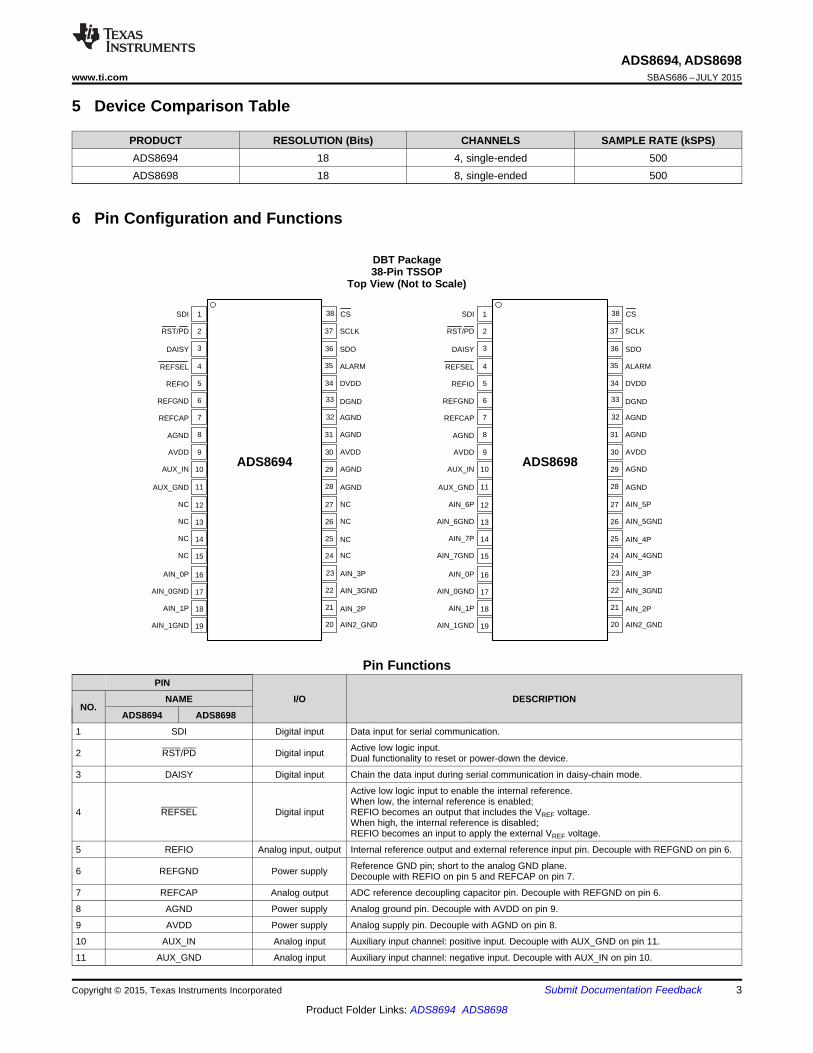
6 Pin Configuration and Functions
DBT Package38-Pin TSSOP
Top View (Not to Scale)
Pin FunctionsPIN
NAME I/O DESCRIPTIONNO.
ADS8694 ADS8698
1 SDI Digital input Data input for serial communication.
Active low logic input.2 RST/PD Digital input Dual functionality to reset or power-down the device.
3 DAISY Digital input Chain the data input during serial communication in daisy-chain mode.
Active low logic input to enable the internal reference.When low, the internal reference is enabled;
4 REFSEL Digital input REFIO becomes an output that includes the VREF voltage.When high, the internal reference is disabled;REFIO becomes an input to apply the external VREF voltage.
5 REFIO Analog input, output Internal reference output and external reference input pin. Decouple with REFGND on pin 6.
Reference GND pin; short to the analog GND plane.6 REFGND Power supply Decouple with REFIO on pin 5 and REFCAP on pin 7.
7 REFCAP Analog output ADC reference decoupling capacitor pin. Decouple with REFGND on pin 6.
8 AGND Power supply Analog ground pin. Decouple with AVDD on pin 9.
9 AVDD Power supply Analog supply pin. Decouple with AGND on pin 8.
10 AUX_IN Analog input Auxiliary input channel: positive input. Decouple with AUX_GND on pin 11.
11 AUX_GND Analog input Auxiliary input channel: negative input. Decouple with AUX_IN on pin 10.
Copyright © 2015, Texas Instruments Incorporated Submit Documentation Feedback 3
Product Folder Links: ADS8694 ADS8698
ADS8694, ADS8698SBAS686 –JULY 2015 www.ti.com
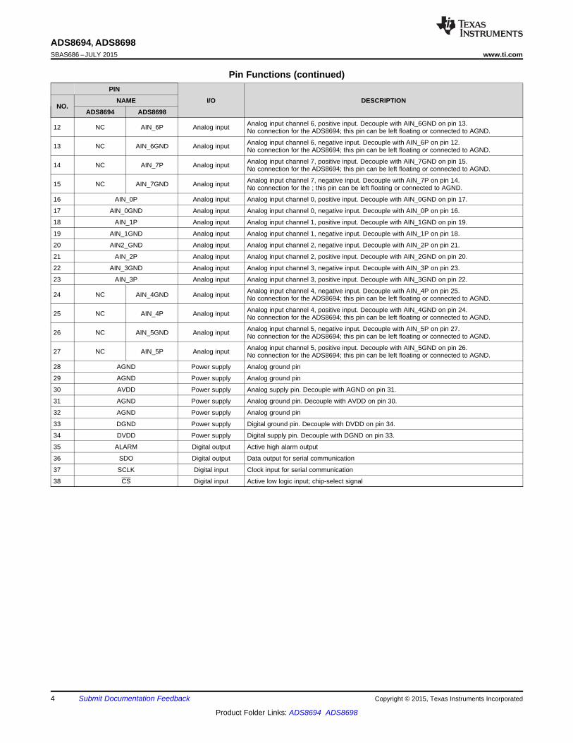
Pin Functions (continued)PIN
NAME I/O DESCRIPTIONNO.
ADS8694 ADS8698
Analog input channel 6, positive input. Decouple with AIN_6GND on pin 13.12 NC AIN_6P Analog input No connection for the ADS8694; this pin can be left floating or connected to AGND.
Analog input channel 6, negative input. Decouple with AIN_6P on pin 12.13 NC AIN_6GND Analog input No connection for the ADS8694; this pin can be left floating or connected to AGND.
Analog input channel 7, positive input. Decouple with AIN_7GND on pin 15.14 NC AIN_7P Analog input No connection for the ADS8694; this pin can be left floating or connected to AGND.
Analog input channel 7, negative input. Decouple with AIN_7P on pin 14.15 NC AIN_7GND Analog input No connection for the ; this pin can be left floating or connected to AGND.
16 AIN_0P Analog input Analog input channel 0, positive input. Decouple with AIN_0GND on pin 17.
17 AIN_0GND Analog input Analog input channel 0, negative input. Decouple with AIN_0P on pin 16.
18 AIN_1P Analog input Analog input channel 1, positive input. Decouple with AIN_1GND on pin 19.
19 AIN_1GND Analog input Analog input channel 1, negative input. Decouple with AIN_1P on pin 18.
20 AIN2_GND Analog input Analog input channel 2, negative input. Decouple with AIN_2P on pin 21.
21 AIN_2P Analog input Analog input channel 2, positive input. Decouple with AIN_2GND on pin 20.
22 AIN_3GND Analog input Analog input channel 3, negative input. Decouple with AIN_3P on pin 23.
23 AIN_3P Analog input Analog input channel 3, positive input. Decouple with AIN_3GND on pin 22.
Analog input channel 4, negative input. Decouple with AIN_4P on pin 25.24 NC AIN_4GND Analog input No connection for the ADS8694; this pin can be left floating or connected to AGND.
Analog input channel 4, positive input. Decouple with AIN_4GND on pin 24.25 NC AIN_4P Analog input No connection for the ADS8694; this pin can be left floating or connected to AGND.
Analog input channel 5, negative input. Decouple with AIN_5P on pin 27.26 NC AIN_5GND Analog input No connection for the ADS8694; this pin can be left floating or connected to AGND.
Analog input channel 5, positive input. Decouple with AIN_5GND on pin 26.27 NC AIN_5P Analog input No connection for the ADS8694; this pin can be left floating or connected to AGND.
28 AGND Power supply Analog ground pin
29 AGND Power supply Analog ground pin
30 AVDD Power supply Analog supply pin. Decouple with AGND on pin 31.
31 AGND Power supply Analog ground pin. Decouple with AVDD on pin 30.
32 AGND Power supply Analog ground pin
33 DGND Power supply Digital ground pin. Decouple with DVDD on pin 34.
34 DVDD Power supply Digital supply pin. Decouple with DGND on pin 33.
35 ALARM Digital output Active high alarm output
36 SDO Digital output Data output for serial communication
37 SCLK Digital input Clock input for serial communication
38 CS Digital input Active low logic input; chip-select signal
4 Submit Documentation Feedback Copyright © 2015, Texas Instruments Incorporated
Product Folder Links: ADS8694 ADS8698
ADS8694, ADS8698www.ti.com SBAS686 –JULY 2015
7 Specifications
7.1 Absolute Maximum Ratingsover operating free-air temperature range (unless otherwise noted) (1)
MIN MAX UNITAIN_nP, AIN_nGND to GND (2) –20 20 VAIN_nP, AIN_nGND to GND (3) –11 11 VAUX_GND to GND –0.3 0.3 VAUX_IN to GND –0.3 AVDD + 0.3 VAVDD to GND or DVDD to GND –0.3 7 VREFCAP to REFGND or REFIO to REFGND –0.3 5.7 VGND to REFGND –0.3 0.3 VDigital input pins to GND –0.3 DVDD + 0.3 VDigital output pins to GND –0.3 DVDD + 0.3 VOperating temperature, TA –40 125 °CStorage temperature, Tstg –65 150 °C
(1) Stresses beyond those listed under Absolute Maximum Ratings may cause permanent damage to the device. These are stress ratingsonly, and do not imply functional operation of the device at these or any other conditions beyond those indicated under RecommendedOperating Conditions. Exposure to absolute-maximum-rated conditions for extended periods may affect device reliability.
(2) AVDD = 5 V or offers a low impedance of < 30 kΩ.(3) AVDD = floating with an impedance > 30 kΩ.
7.2 ESD RatingsVALUE UNIT
Analog input pins ±4000(AIN_nP; AIN_nGND)Human body model (HBM), per ANSI/ESDA/JEDEC JS-001 (1)ElectrostaticV(ESD) Vdischarge All other pins ±2000Charged device model (CDM), per JEDEC specification JESD22-C101 (2) ±500
(1) JEDEC document JEP155 states that 500-V HBM allows safe manufacturing with a standard ESD control process.(2) JEDEC document JEP157 states that 250-V CDM allows safe manufacturing with a standard ESD control process.
7.3 Recommended Operating Conditionsover operating free-air temperature range (unless otherwise noted)
MIN NOM MAX UNITAVDD Analog supply voltage 4.75 5 5.25 VDVDD Digital supply voltage 1.65 3.3 AVDD V
7.4 Thermal InformationADS8694,ADS8698
THERMAL METRIC (1) UNITDBT (TSSOP)38 PINS
RθJA Junction-to-ambient thermal resistance 68.8 °C/WRθJC(top) Junction-to-case (top) thermal resistance 19.9 °C/WRθJB Junction-to-board thermal resistance 30.4 °C/WψJT Junction-to-top characterization parameter 1.3 °C/WψJB Junction-to-board characterization parameter 29.8 °C/WRθJC(bot) Junction-to-case (bottom) thermal resistance NA °C/W
(1) For more information about traditional and new thermal metrics, see the IC Package Thermal Metrics application report, SPRA953.
Copyright © 2015, Texas Instruments Incorporated Submit Documentation Feedback 5
Product Folder Links: ADS8694 ADS8698
ADS8694, ADS8698SBAS686 –JULY 2015 www.ti.com
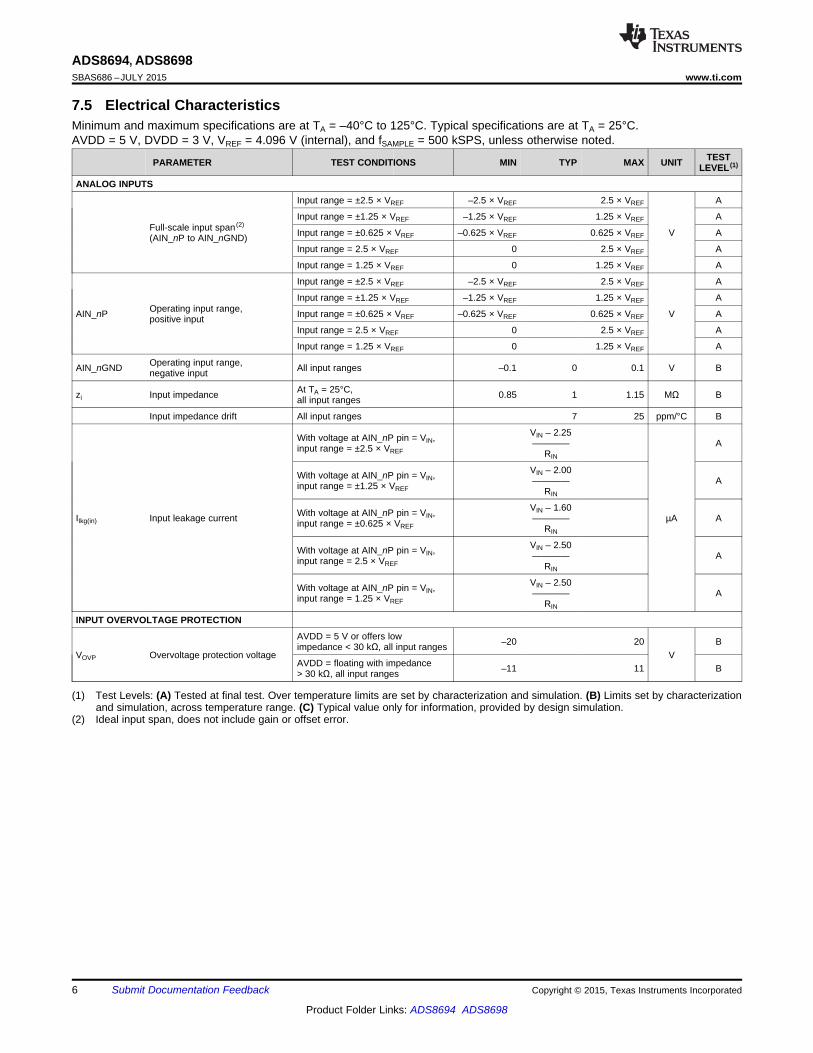
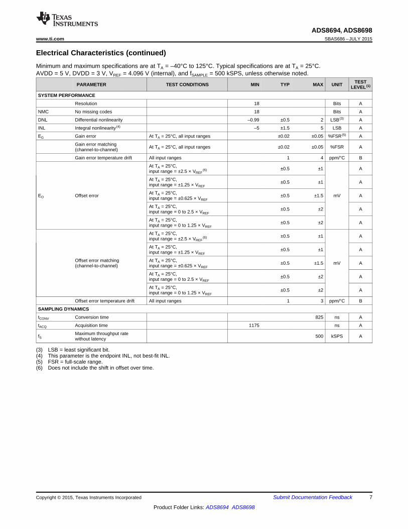
7.5 Electrical CharacteristicsMinimum and maximum specifications are at TA = –40°C to 125°C. Typical specifications are at TA = 25°C.AVDD = 5 V, DVDD = 3 V, VREF = 4.096 V (internal), and fSAMPLE = 500 kSPS, unless otherwise noted.
TESTPARAMETER TEST CONDITIONS MIN TYP MAX UNIT LEVEL (1)
ANALOG INPUTS
Input range = ±2.5 × VREF –2.5 × VREF 2.5 × VREF A
Input range = ±1.25 × VREF –1.25 × VREF 1.25 × VREF AFull-scale input span (2)
Input range = ±0.625 × VREF –0.625 × VREF 0.625 × VREF V A(AIN_nP to AIN_nGND)Input range = 2.5 × VREF 0 2.5 × VREF A
Input range = 1.25 × VREF 0 1.25 × VREF A
Input range = ±2.5 × VREF –2.5 × VREF 2.5 × VREF A
Input range = ±1.25 × VREF –1.25 × VREF 1.25 × VREF AOperating input range,AIN_nP Input range = ±0.625 × VREF –0.625 × VREF 0.625 × VREF V Apositive input
Input range = 2.5 × VREF 0 2.5 × VREF A
Input range = 1.25 × VREF 0 1.25 × VREF A
Operating input range,AIN_nGND All input ranges –0.1 0 0.1 V Bnegative input
At TA = 25°C,zi Input impedance 0.85 1 1.15 MΩ Ball input ranges
Input impedance drift All input ranges 7 25 ppm/°C B
VIN – 2.25With voltage at AIN_nP pin = VIN, ———— Ainput range = ±2.5 × VREF RIN
VIN – 2.00With voltage at AIN_nP pin = VIN, ———— Ainput range = ±1.25 × VREF RIN
VIN – 1.60With voltage at AIN_nP pin = VIN,IIkg(in) Input leakage current ———— µA Ainput range = ±0.625 × VREF RIN
VIN – 2.50With voltage at AIN_nP pin = VIN, ———— Ainput range = 2.5 × VREF RIN
VIN – 2.50With voltage at AIN_nP pin = VIN, ———— Ainput range = 1.25 × VREF RIN
INPUT OVERVOLTAGE PROTECTION
AVDD = 5 V or offers low –20 20 Bimpedance < 30 kΩ, all input rangesVOVP Overvoltage protection voltage V
AVDD = floating with impedance –11 11 B> 30 kΩ, all input ranges
(1) Test Levels: (A) Tested at final test. Over temperature limits are set by characterization and simulation. (B) Limits set by characterizationand simulation, across temperature range. (C) Typical value only for information, provided by design simulation.
(2) Ideal input span, does not include gain or offset error.
6 Submit Documentation Feedback Copyright © 2015, Texas Instruments Incorporated
Product Folder Links: ADS8694 ADS8698
ADS8694, ADS8698www.ti.com SBAS686 –JULY 2015
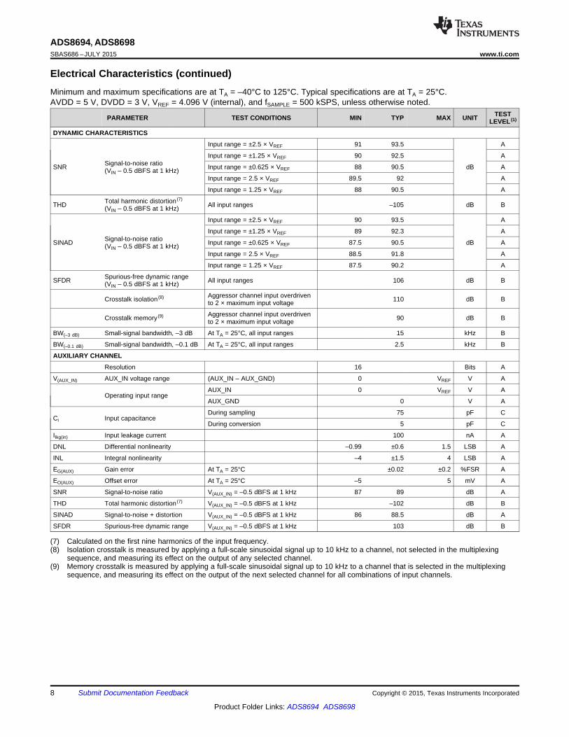
Electrical Characteristics (continued)Minimum and maximum specifications are at TA = –40°C to 125°C. Typical specifications are at TA = 25°C.AVDD = 5 V, DVDD = 3 V, VREF = 4.096 V (internal), and fSAMPLE = 500 kSPS, unless otherwise noted.
TESTPARAMETER TEST CONDITIONS MIN TYP MAX UNIT LEVEL (1)
SYSTEM PERFORMANCE
Resolution 18 Bits A
NMC No missing codes 18 Bits A
DNL Differential nonlinearity –0.99 ±0.5 2 LSB (3) A
INL Integral nonlinearity (4) –5 ±1.5 5 LSB A
EG Gain error At TA = 25°C, all input ranges ±0.02 ±0.05 %FSR (5) A
Gain error matching At TA = 25°C, all input ranges ±0.02 ±0.05 %FSR A(channel-to-channel)
Gain error temperature drift All input ranges 1 4 ppm/°C B
At TA = 25°C, ±0.5 ±1 Ainput range = ±2.5 × VREF(6)
At TA = 25°C, ±0.5 ±1 Ainput range = ±1.25 × VREF
At TA = 25°C,EO Offset error ±0.5 ±1.5 mV Ainput range = ±0.625 × VREF
At TA = 25°C, ±0.5 ±2 Ainput range = 0 to 2.5 × VREF
At TA = 25°C, ±0.5 ±2 Ainput range = 0 to 1.25 × VREF
At TA = 25°C, ±0.5 ±1 Ainput range = ±2.5 × VREF(6)
At TA = 25°C, ±0.5 ±1 Ainput range = ±1.25 × VREF
Offset error matching At TA = 25°C, ±0.5 ±1.5 mV A(channel-to-channel) input range = ±0.625 × VREF
At TA = 25°C, ±0.5 ±2 Ainput range = 0 to 2.5 × VREF
At TA = 25°C, ±0.5 ±2 Ainput range = 0 to 1.25 × VREF
Offset error temperature drift All input ranges 1 3 ppm/°C B
SAMPLING DYNAMICS
tCONV Conversion time 825 ns A
tACQ Acquisition time 1175 ns A
Maximum throughput ratefS 500 kSPS Awithout latency
(3) LSB = least significant bit.(4) This parameter is the endpoint INL, not best-fit INL.(5) FSR = full-scale range.(6) Does not include the shift in offset over time.
Copyright © 2015, Texas Instruments Incorporated Submit Documentation Feedback 7
Product Folder Links: ADS8694 ADS8698
ADS8694, ADS8698SBAS686 –JULY 2015 www.ti.com
Electrical Characteristics (continued)Minimum and maximum specifications are at TA = –40°C to 125°C. Typical specifications are at TA = 25°C.AVDD = 5 V, DVDD = 3 V, VREF = 4.096 V (internal), and fSAMPLE = 500 kSPS, unless otherwise noted.
TESTPARAMETER TEST CONDITIONS MIN TYP MAX UNIT LEVEL (1)
DYNAMIC CHARACTERISTICS
Input range = ±2.5 × VREF 91 93.5 A
Input range = ±1.25 × VREF 90 92.5 ASignal-to-noise ratioSNR Input range = ±0.625 × VREF 88 90.5 dB A(VIN – 0.5 dBFS at 1 kHz)
Input range = 2.5 × VREF 89.5 92 A
Input range = 1.25 × VREF 88 90.5 A
Total harmonic distortion (7)THD All input ranges –105 dB B(VIN – 0.5 dBFS at 1 kHz)
Input range = ±2.5 × VREF 90 93.5 A
Input range = ±1.25 × VREF 89 92.3 ASignal-to-noise ratioSINAD Input range = ±0.625 × VREF 87.5 90.5 dB A(VIN – 0.5 dBFS at 1 kHz)
Input range = 2.5 × VREF 88.5 91.8 A
Input range = 1.25 × VREF 87.5 90.2 A
Spurious-free dynamic rangeSFDR All input ranges 106 dB B(VIN – 0.5 dBFS at 1 kHz)
Aggressor channel input overdrivenCrosstalk isolation (8) 110 dB Bto 2 × maximum input voltage
Aggressor channel input overdrivenCrosstalk memory (9) 90 dB Bto 2 × maximum input voltage
BW(–3 dB) Small-signal bandwidth, –3 dB At TA = 25°C, all input ranges 15 kHz B
BW(–0.1 dB) Small-signal bandwidth, –0.1 dB At TA = 25°C, all input ranges 2.5 kHz B
AUXILIARY CHANNEL
Resolution 16 Bits A
V(AUX_IN) AUX_IN voltage range (AUX_IN – AUX_GND) 0 VREF V A
AUX_IN 0 VREF V AOperating input range
AUX_GND 0 V A
During sampling 75 pF CCi Input capacitance
During conversion 5 pF C
IIkg(in) Input leakage current 100 nA A
DNL Differential nonlinearity –0.99 ±0.6 1.5 LSB A
INL Integral nonlinearity –4 ±1.5 4 LSB A
EG(AUX) Gain error At TA = 25°C ±0.02 ±0.2 %FSR A
EO(AUX) Offset error At TA = 25°C –5 5 mV A
SNR Signal-to-noise ratio V(AUX_IN) = –0.5 dBFS at 1 kHz 87 89 dB A
THD Total harmonic distortion (7) V(AUX_IN) = –0.5 dBFS at 1 kHz –102 dB B
SINAD Signal-to-noise + distortion V(AUX_IN) = –0.5 dBFS at 1 kHz 86 88.5 dB A
SFDR Spurious-free dynamic range V(AUX_IN) = –0.5 dBFS at 1 kHz 103 dB B
(7) Calculated on the first nine harmonics of the input frequency.(8) Isolation crosstalk is measured by applying a full-scale sinusoidal signal up to 10 kHz to a channel, not selected in the multiplexing
sequence, and measuring its effect on the output of any selected channel.(9) Memory crosstalk is measured by applying a full-scale sinusoidal signal up to 10 kHz to a channel that is selected in the multiplexing
sequence, and measuring its effect on the output of the next selected channel for all combinations of input channels.
8 Submit Documentation Feedback Copyright © 2015, Texas Instruments Incorporated
Product Folder Links: ADS8694 ADS8698
ADS8694, ADS8698www.ti.com SBAS686 –JULY 2015
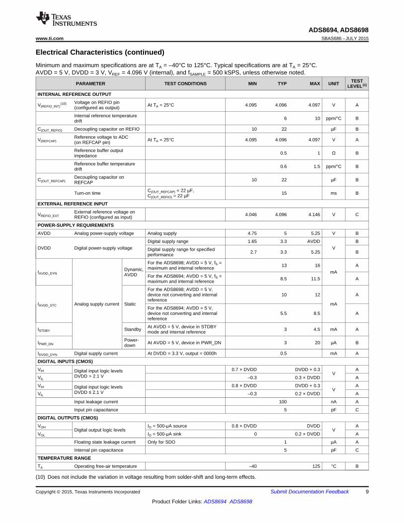
Electrical Characteristics (continued)Minimum and maximum specifications are at TA = –40°C to 125°C. Typical specifications are at TA = 25°C.AVDD = 5 V, DVDD = 3 V, VREF = 4.096 V (internal), and fSAMPLE = 500 kSPS, unless otherwise noted.
TESTPARAMETER TEST CONDITIONS MIN TYP MAX UNIT LEVEL (1)
INTERNAL REFERENCE OUTPUT
Voltage on REFIO pinV(REFIO_INT)(10) At TA = 25°C 4.095 4.096 4.097 V A(configured as output)
Internal reference temperature 6 10 ppm/°C Bdrift
C(OUT_REFIO) Decoupling capacitor on REFIO 10 22 µF B
Reference voltage to ADCV(REFCAP) At TA = 25°C 4.095 4.096 4.097 V A(on REFCAP pin)
Reference buffer output 0.5 1 Ω Bimpedance
Reference buffer temperature 0.6 1.5 ppm/°C Bdrift
Decoupling capacitor onC(OUT_REFCAP) 10 22 μF BREFCAP
C(OUT_REFCAP) = 22 µF,Turn-on time 15 ms BC(OUT_REFIO) = 22 µF
EXTERNAL REFERENCE INPUT
External reference voltage onVREFIO_EXT 4.046 4.096 4.146 V CREFIO (configured as input)
POWER-SUPPLY REQUIREMENTS
AVDD Analog power-supply voltage Analog supply 4.75 5 5.25 V B
Digital supply range 1.65 3.3 AVDD BDVDD Digital power-supply voltage VDigital supply range for specified 2.7 3.3 5.25 Bperformance
For the ADS8698; AVDD = 5 V, fS = 13 16 Amaximum and internal referenceDynamic,IAVDD_DYN mAAVDD For the ADS8694; AVDD = 5 V, fS = 8.5 11.5 Amaximum and internal reference
For the ADS8698; AVDD = 5 V,device not converting and internal 10 12 Areference
IAVDD_STC Analog supply current Static mAFor the ADS8694; AVDD = 5 V,device not converting and internal 5.5 8.5 Areference
At AVDD = 5 V, device in STDBYISTDBY Standby 3 4.5 mA Amode and internal reference
Power-IPWR_DN At AVDD = 5 V, device in PWR_DN 3 20 μA Bdown
IDVDD_DYN Digital supply current At DVDD = 3.3 V, output = 0000h 0.5 mA A
DIGITAL INPUTS (CMOS)
VIH 0.7 × DVDD DVDD + 0.3 ADigital input logic levels VDVDD > 2.1 VVIL –0.3 0.3 × DVDD A
VIH 0.8 × DVDD DVDD + 0.3 ADigital input logic levels VDVDD ≤ 2.1 VVIL –0.3 0.2 × DVDD A
Input leakage current 100 nA A
Input pin capacitance 5 pF C
DIGITAL OUTPUTS (CMOS)
VOH IO = 500-μA source 0.8 × DVDD DVDD ADigital output logic levels V
VOL IO = 500-μA sink 0 0.2 × DVDD A
Floating state leakage current Only for SDO 1 µA A
Internal pin capacitance 5 pF C
TEMPERATURE RANGE
TA Operating free-air temperature –40 125 °C B
(10) Does not include the variation in voltage resulting from solder-shift and long-term effects.
Copyright © 2015, Texas Instruments Incorporated Submit Documentation Feedback 9
Product Folder Links: ADS8694 ADS8698
1 2 14 15 16 17 25 26 27 28 29 30 31 32SCLK
CS
D9#2
D8#2
D7#2
D6#2
D5#2
D4#2SDO
tSU_CSCK
tDV_CSDOtHT_CKDO tSU_DOCK tDZ_CSDO
Sample N
Sample N + 1
tACQtCONV
tS
Data from sample N
tPH_CS
33 34
D17#2
D16#2
18
D3#2
D2#2
D1#2
D0#2
B15 B14 B2 B1 B0 X X X X X XSDI X X X X X X
tPH_CK tPL_CK tSCLK
tSU_DICK tHT_CKDI
tD_CKCS
7 8 9
B9 B8 B7B10 B3
D9#1
D8#1
D7#1
D6#1
D5#1
D4#1DAISY
D17#1
D16#1
D3#1
D2#1
D1#1
D0#1
tHT_CKDSYtSU_DSYCK
ADS8694, ADS8698SBAS686 –JULY 2015 www.ti.com
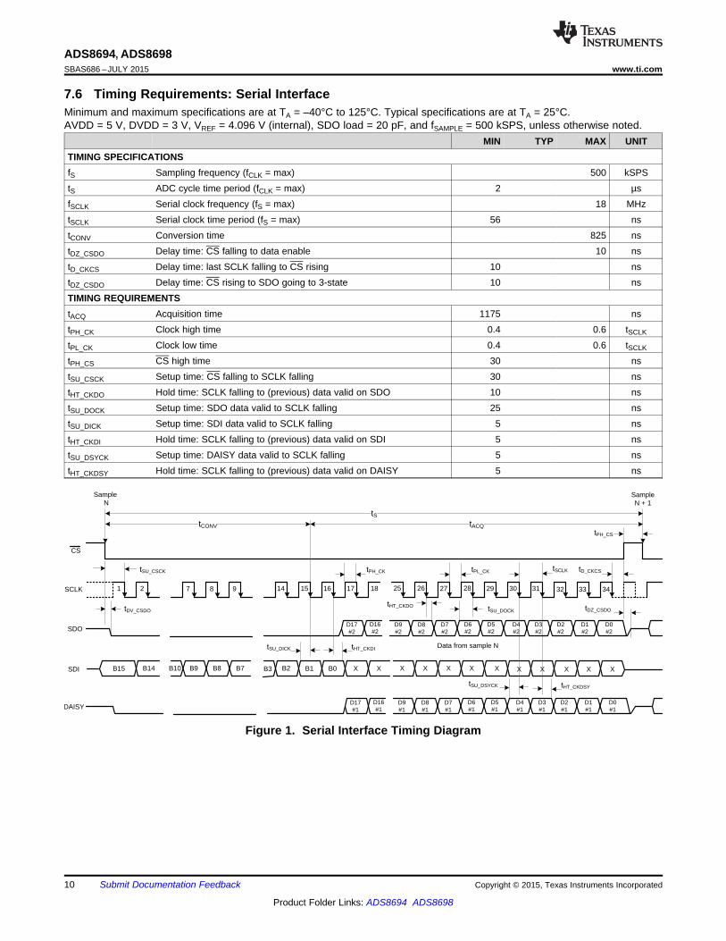
7.6 Timing Requirements: Serial InterfaceMinimum and maximum specifications are at TA = –40°C to 125°C. Typical specifications are at TA = 25°C.AVDD = 5 V, DVDD = 3 V, VREF = 4.096 V (internal), SDO load = 20 pF, and fSAMPLE = 500 kSPS, unless otherwise noted.
MIN TYP MAX UNITTIMING SPECIFICATIONSfS Sampling frequency (fCLK = max) 500 kSPStS ADC cycle time period (fCLK = max) 2 µsfSCLK Serial clock frequency (fS = max) 18 MHztSCLK Serial clock time period (fS = max) 56 nstCONV Conversion time 825 nstDZ_CSDO Delay time: CS falling to data enable 10 nstD_CKCS Delay time: last SCLK falling to CS rising 10 nstDZ_CSDO Delay time: CS rising to SDO going to 3-state 10 nsTIMING REQUIREMENTStACQ Acquisition time 1175 nstPH_CK Clock high time 0.4 0.6 tSCLK
tPL_CK Clock low time 0.4 0.6 tSCLK
tPH_CS CS high time 30 nstSU_CSCK Setup time: CS falling to SCLK falling 30 nstHT_CKDO Hold time: SCLK falling to (previous) data valid on SDO 10 nstSU_DOCK Setup time: SDO data valid to SCLK falling 25 nstSU_DICK Setup time: SDI data valid to SCLK falling 5 nstHT_CKDI Hold time: SCLK falling to (previous) data valid on SDI 5 nstSU_DSYCK Setup time: DAISY data valid to SCLK falling 5 nstHT_CKDSY Hold time: SCLK falling to (previous) data valid on DAISY 5 ns
Figure 1. Serial Interface Timing Diagram
10 Submit Documentation Feedback Copyright © 2015, Texas Instruments Incorporated
Product Folder Links: ADS8694 ADS8698
0
5000
10000
15000
20000
25000
30000
131062 131065 131068 131071 131074 131077 131080
Num
ber
of H
its
Output Codes C007
0
6000
12000
18000
24000
131061 131065 131069 131073 131077 131081
Num
ber
of H
its
Output Codes C008
±70
0
70
140
210
280
350
±40 ±7 26 59 92 125
Inpu
t Im
peda
nce
Var
iatio
n (
)
Free-Air Temperature (oC) C005
----- ± 2.5*VREF ----- � 1.25*VREF ----- � 0.625*VREF ----- + 2.5*VREF -----+1.25*VREF
0
160
320
480
640
800
0.85 0.88 0.91 0.94 0.97 1 1.03 1.06 1.09 1.12 1.15
Num
ber
of S
ampl
es
Input Impedance (M ) C006
±15
±9
±3
3
9
15
±10 ±6 ±2 2 6 10
Ana
log
Inpu
t Cur
rent
(µ
A)
Input Voltage (V) C001
----- ± 2.5*VREF ----- � 1.25*VREF ----- � 0.625*VREF ----- + 2.5*VREF -----+1.25*VREF
±15
±9
±3
3
9
15
±10 ±6 ±2 2 6 10
Ana
log
Inpu
t Cur
rent
(µ
A)
Input Voltage (V) C002
------- 250C --------400C --------1250C
ADS8694, ADS8698www.ti.com SBAS686 –JULY 2015
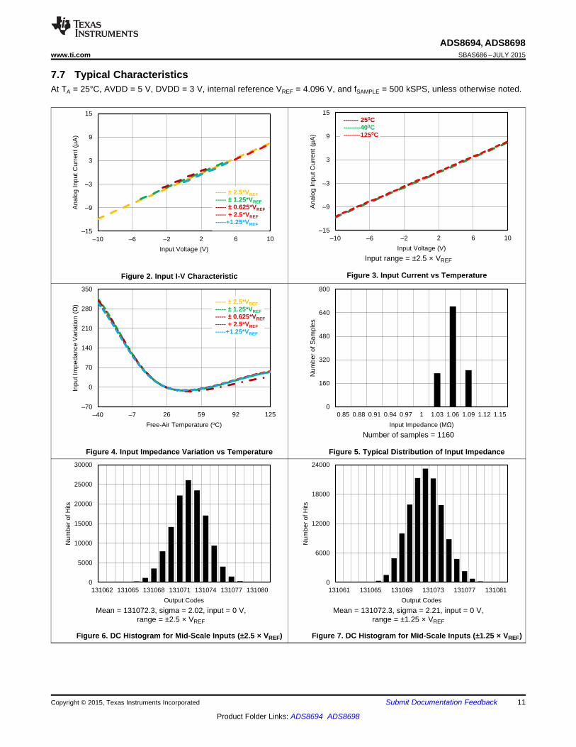
7.7 Typical CharacteristicsAt TA = 25°C, AVDD = 5 V, DVDD = 3 V, internal reference VREF = 4.096 V, and fSAMPLE = 500 kSPS, unless otherwise noted.
Input range = ±2.5 × VREF
Figure 3. Input Current vs TemperatureFigure 2. Input I-V Characteristic
Number of samples = 1160
Figure 4. Input Impedance Variation vs Temperature Figure 5. Typical Distribution of Input Impedance
Mean = 131072.3, sigma = 2.02, input = 0 V, Mean = 131072.3, sigma = 2.21, input = 0 V,range = ±2.5 × VREF range = ±1.25 × VREF
Figure 6. DC Histogram for Mid-Scale Inputs (±2.5 × VREF) Figure 7. DC Histogram for Mid-Scale Inputs (±1.25 × VREF)
Copyright © 2015, Texas Instruments Incorporated Submit Documentation Feedback 11
Product Folder Links: ADS8694 ADS8698
-1
-0.6
-0.2
0.2
0.6
1
1.4
±40 ±7 26 59 92 125
Diff
eren
tial N
onlin
earit
y (L
SB
)
Free-Air Temperature (oC) C013
Maximum
Minimum
-2
-1
0
1
2
0 65536 131072 196608 262144
Inte
gral
Non
linea
rity
(LS
B)
Codes (LSB) C014
0
4000
8000
12000
16000
20000
131058 131063 131068 131073 131078 131083
Num
ber
of H
its
Output Codes C011
-1
-0.6
-0.2
0.2
0.6
1
1.4
0 65536 131072 196608 262144
Diff
eren
tial N
onlin
earit
y (L
SB
)
Codes (LSB) C012
0
6000
12000
18000
24000
131059 131063 131067 131071 131075 131079 131083
Num
ber
of H
its
Output Codes C009
0
6000
12000
18000
24000
131060 131064 131068 131072 131076 131080
Num
ber
of H
its
Output Codes C010
ADS8694, ADS8698SBAS686 –JULY 2015 www.ti.com
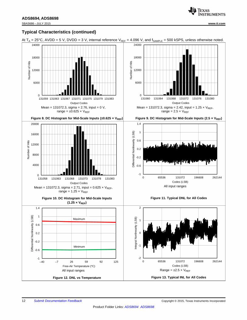
Typical Characteristics (continued)At TA = 25°C, AVDD = 5 V, DVDD = 3 V, internal reference VREF = 4.096 V, and fSAMPLE = 500 kSPS, unless otherwise noted.
Mean = 131072.3, sigma = 2.76, input = 0 V, Mean = 131072.3, sigma = 2.42, input = 1.25 × VREF,range = ±0.625 × VREF range = 2.5 × VREF
Figure 8. DC Histogram for Mid-Scale Inputs (±0.625 × VREF) Figure 9. DC Histogram for Mid-Scale Inputs (2.5 × VREF)
All input rangesMean = 131072.3, sigma = 2.71, input = 0.625 × VREF,range = 1.25 × VREF
Figure 11. Typical DNL for All CodesFigure 10. DC Histogram for Mid-Scale Inputs(1.25 × VREF)
Range = ±2.5 × VREFAll input ranges
Figure 13. Typical INL for All CodesFigure 12. DNL vs Temperature
12 Submit Documentation Feedback Copyright © 2015, Texas Instruments Incorporated
Product Folder Links: ADS8694 ADS8698
±2
±1
0
1
2
±40 ±7 26 59 92 125
Inte
gral
Non
linea
rity
(LS
B)
Free-Air Temperature (oC) C019
Maximum
Minimum
±2
±1
0
1
2
±40 ±7 26 59 92 125
Inte
gral
Non
linea
rity
(LS
B)
Free-AirTemperature (oC) C020
Maximum
Minimum
-2
-1.5
-1
-0.5
0
0.5
1
1.5
2
0 65536 131072 196608 262144
Inte
gral
Non
linea
rity
(LS
B)
Codes (LSB) C017
-2
-1.5
-1
-0.5
0
0.5
1
1.5
2
0 65536 131072 196608 262144
Inte
gral
Non
linea
rity
(LS
B)
Codes (LSB) C018
-2
-1.5
-1
-0.5
0
0.5
1
1.5
2
0 65536 131072 196608 262144
Inte
gral
Non
linea
rity
(LS
B)
Codes (LSB) C015
-2
-1.5
-1
-0.5
0
0.5
1
1.5
2
0 65536 131072 196608 262144
Inte
gral
Non
linea
rity
(LS
B)
Codes (LSB) C016
ADS8694, ADS8698www.ti.com SBAS686 –JULY 2015
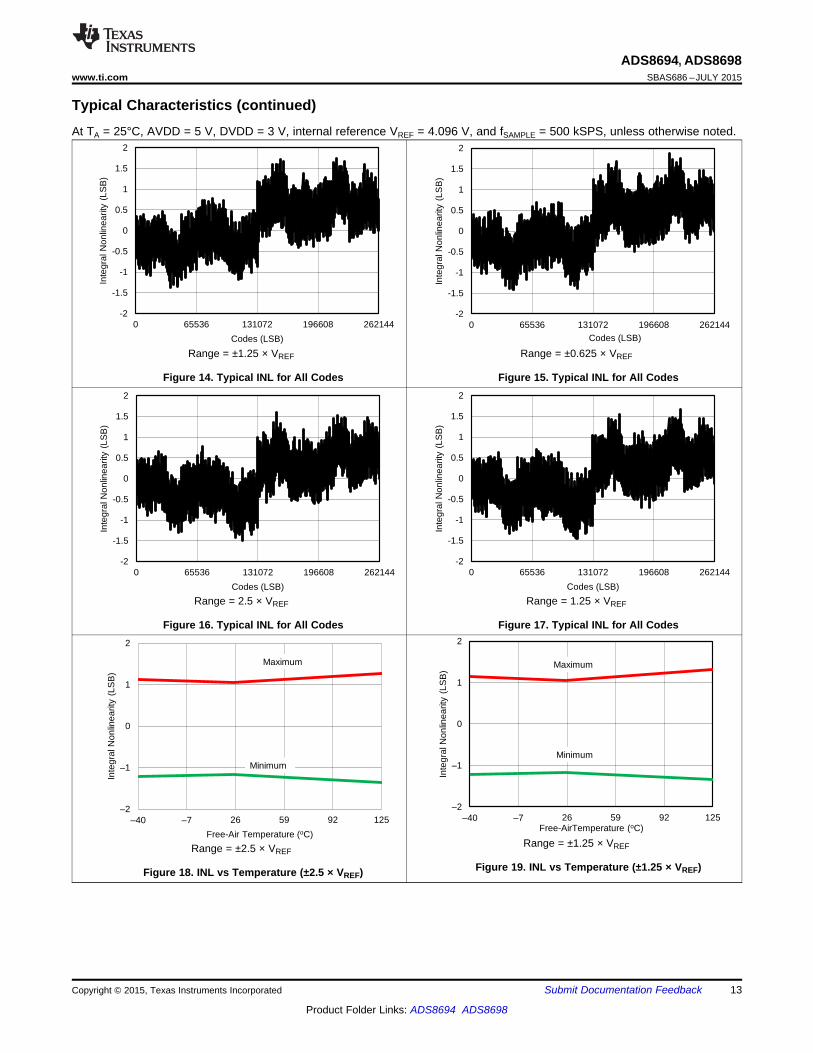
Typical Characteristics (continued)At TA = 25°C, AVDD = 5 V, DVDD = 3 V, internal reference VREF = 4.096 V, and fSAMPLE = 500 kSPS, unless otherwise noted.
Range = ±1.25 × VREF Range = ±0.625 × VREF
Figure 14. Typical INL for All Codes Figure 15. Typical INL for All Codes
Range = 2.5 × VREF Range = 1.25 × VREF
Figure 16. Typical INL for All Codes Figure 17. Typical INL for All Codes
Range = ±1.25 × VREFRange = ±2.5 × VREF
Figure 19. INL vs Temperature (±1.25 × VREF)Figure 18. INL vs Temperature (±2.5 × VREF)
Copyright © 2015, Texas Instruments Incorporated Submit Documentation Feedback 13
Product Folder Links: ADS8694 ADS8698
0
20
40
60
80
0 0.2 0.4 0.6 0.8 1 1.2 1.4 1.6 1.8 2 2.2 2.4 2.6 2.8 3
Num
ber
of D
evic
es
Offset Drift (ppm/oC) C025
-1
-0.75
-0.5
-0.25
0
0.25
0.5
0.75
1
±40 ±7 26 59 92 125
Offs
et E
rror
(m
V)
Free-Air Temperature (oC) C026
......CH0, .......CH1, ......CH2,
.......CH3, ......CH4, .......CH5,
........CH6, .......CH7
±2
±1
0
1
2
±40 ±7 26 59 92 125
Inte
gral
Non
linea
rity
(LS
B)
Free-Air Temperature (oC) C022
Maximum
Minimum
-1
-0.75
-0.5
-0.25
0
0.25
0.5
0.75
1
±40 ±7 26 59 92 125
Offs
et E
rror
(m
V)
Free-Air Temperature (oC) C024
----- ± 2.5*VREF ----- � 1.25*VREF ----- � 0.625*VREF ----- + 2.5*VREF -----+1.25*VREF
±2
±1
0
1
2
±40 ±7 26 59 92 125
Inte
gral
Non
linea
rity
(LS
B)
Free-AirTemperature (oC) C020
Maximum
Minimum
±2
±1
0
1
2
±40 ±7 26 59 92 125
Inte
gral
Non
linea
rity
(LS
B)
Free-Air Temperature (oC) C021
Maximum
Minimum
ADS8694, ADS8698SBAS686 –JULY 2015 www.ti.com
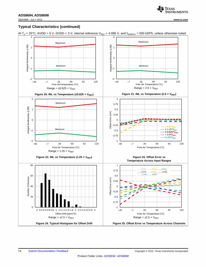
Typical Characteristics (continued)At TA = 25°C, AVDD = 5 V, DVDD = 3 V, internal reference VREF = 4.096 V, and fSAMPLE = 500 kSPS, unless otherwise noted.
Range = 2.5 × VREFRange = ±0.625 × VREF
Figure 21. INL vs Temperature (2.5 × VREF)Figure 20. INL vs Temperature (±0.625 × VREF)
Range = 1.25 × VREF
Figure 22. INL vs Temperature (1.25 × VREF) Figure 23. Offset Error vsTemperature Across Input Ranges
Range = ±2.5 × VREF Range = ±2.5 × VREF
Figure 24. Typical Histogram for Offset Drift Figure 25. Offset Error vs Temperature Across Channels
14 Submit Documentation Feedback Copyright © 2015, Texas Instruments Incorporated
Product Folder Links: ADS8694 ADS8698
±200
±160
±120
±80
±40
0
0 50000 100000 150000 200000 250000
Am
plitu
de (
dB)
Input Frequency (Hz) C031
±200
±160
±120
±80
±40
0
0 50000 100000 150000 200000 250000
Am
plitu
de (
dB)
Input Frequency (Hz) C032
-0.5
0
0.5
1
1.5
2
0 4 8 12 16 20
Gai
n (%
FS
)
Source Resistance (k ) C030
----- ± 2.5*VREF ----- � 1.25*VREF ----- � 0.625*VREF ----- + 2.5*VREF -----+1.25*VREF
-0.05
-0.03
-0.01
0.01
0.03
0.05
±40 ±7 26 59 92 125
Gai
n (%
FS
)
Free-Air Temperature (oC) C029
......CH0, .......CH1, ......CH2,
.......CH3, ......CH4, .......CH5,
........CH6, .......CH7
0
20
40
60
80
100
0 0.5 1 1.5 2 2.5 3 3.5 4
Num
ber
of U
nits
Gain Drift (ppm/oC) C028
-0.05
-0.03
-0.01
0.01
0.03
0.05
±40 ±7 26 59 92 125
Gai
n (%
FS
)
Free-Air temperature (oC) C027
----- ± 2.5*VREF ----- � 1.25*VREF ----- � 0.625*VREF ----- + 2.5*VREF -----+1.25*VREF
ADS8694, ADS8698www.ti.com SBAS686 –JULY 2015
Typical Characteristics (continued)At TA = 25°C, AVDD = 5 V, DVDD = 3 V, internal reference VREF = 4.096 V, and fSAMPLE = 500 kSPS, unless otherwise noted.
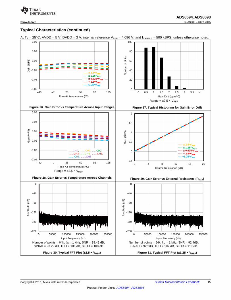
Range = ±2.5 × VREF
Figure 26. Gain Error vs Temperature Across Input Ranges Figure 27. Typical Histogram for Gain Error Drift
Range = ±2.5 × VREF
Figure 28. Gain Error vs Temperature Across Channels Figure 29. Gain Error vs External Resistance (REXT)
Number of points = 64k, fIN = 1 kHz, SNR = 93.48 dB, Number of points = 64k, fIN = 1 kHz, SNR = 92.4dB,SINAD = 93.29 dB, THD = 106 dB, SFDR = 108 dB SINAD = 92.2dB, THD = 107 dB, SFDR = 110 dB
Figure 30. Typical FFT Plot (±2.5 × VREF) Figure 31. Typical FFT Plot (±1.25 × VREF)
Copyright © 2015, Texas Instruments Incorporated Submit Documentation Feedback 15
Product Folder Links: ADS8694 ADS8698
88
90
92
94
96
98
±40 ±7 26 59 92 125
Sig
nal-t
o-N
oise
Rat
io (
dB)
Free-Air Temperature (oC) C037
----- ± 2.5*VREF ----- � 1.25*VREF ----- � 0.625*VREF ----- + 2.5*VREF -----+1.25*VREF
85
86
87
88
89
90
91
92
93
94
100 1000 10000
Sig
nal-t
o-N
oise
+ D
isto
rtio
n R
atio
(dB
)
Input Frequency (Hz) C038
----- ± 2.5*VREF ----- � 1.25*VREF ----- � 0.625*VREF ----- + 2.5*VREF -----+1.25*VREF
±200
±160
±120
±80
±40
0
0 50000 100000 150000 200000 250000
Am
plitu
de (
dB)
Input Frequency (Hz) C035
88.0
89.0
90.0
91.0
92.0
93.0
94.0
100 1000 10000
Sig
nal-t
o-N
oise
Rat
io (
dB)
Input Frequency (Hz) C036
----- ± 2.5*VREF ----- � 1.25*VREF ----- � 0.625*VREF ----- + 2.5*VREF -----+1.25*VREF
±200
±160
±120
±80
±40
0
0 50000 100000 150000 200000 250000
Am
plitu
de (
dB)
Input Frequency (Hz) C033
±200
±160
±120
±80
±40
0
0 50000 100000 150000 200000 250000
Am
plitu
de (
dB)
Input Frequency (Hz) C034
ADS8694, ADS8698SBAS686 –JULY 2015 www.ti.com
Typical Characteristics (continued)At TA = 25°C, AVDD = 5 V, DVDD = 3 V, internal reference VREF = 4.096 V, and fSAMPLE = 500 kSPS, unless otherwise noted.
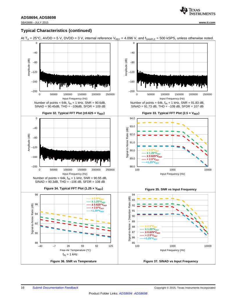
Number of points = 64k, fIN = 1 kHz, SNR = 90.6dB, Number of points = 64k, fIN = 1 kHz, SNR = 91.83 dB,SINAD = 90.45dB, THD = –106dB, SFDR = 109 dB SINAD = 91.73 dB, THD = –108 dB, SFDR = 107 dB
Figure 32. Typical FFT Plot (±0.625 × VREF) Figure 33. Typical FFT Plot (2.5 × VREF)
Number of points = 64k, fIN = 1 kHz, SNR = 90.55 dB,SINAD = 90.3dB, THD = –106 dB, SFDR = 108 dB
Figure 34. Typical FFT Plot (1.25 × VREF) Figure 35. SNR vs Input Frequency
fIN = 1 kHz
Figure 36. SNR vs Temperature Figure 37. SINAD vs Input Frequency
16 Submit Documentation Feedback Copyright © 2015, Texas Instruments Incorporated
Product Folder Links: ADS8694 ADS8698
±140
±125
±110
±95
±80
50 500 5000 50000 500000 5000000
Isol
atio
n C
ross
talk
(dB
)
Input Frequency (Hz) C043
----- ± 2.5*VREF ----- � 1.25*VREF ----- � 0.625*VREF ----- + 2.5*VREF -----+1.25*VREF
±140
±125
±110
±95
±80
50 500 5000 50000 500000 5000000
Mem
ory
Cro
ssta
lk (
dB)
Input Frequency (Hz) C044
----- ± 2.5*VREF ----- � 1.25*VREF ----- � 0.625*VREF ----- + 2.5*VREF -----+1.25*VREF
±120
±110
±100
±90
±80
±40 ±7 26 59 92 125
Tot
al H
arm
onic
Dis
tort
ion
(dB
)
Free-Air Temperature (oC) C041
----- ± 2.5*VREF ----- � 1.25*VREF ----- � 0.625*VREF ----- + 2.5*VREF -----+1.25*VREF
±140
±125
±110
±95
±80
50 500 5000 50000 500000 5000000
Mem
ory
Cro
ssta
lk (
dB)
Input Frequency (Hz) C042
----- ± 2.5*VREF ----- � 1.25*VREF ----- � 0.625*VREF ----- + 2.5*VREF -----+1.25*VREF
±120
±110
±100
±90
±80
10 2010 4010 6010 8010 10010
Tot
al H
arm
onic
Dis
tort
ion
(dB
)
Input Frequency (Hz) C040
----- ± 2.5*VREF ----- � 1.25*VREF ----- � 0.625*VREF ----- + 2.5*VREF -----+1.25*VREF
88
89
90
91
92
93
94
95
±40 ±7 26 59 92 125
Sig
nal-t
o-N
oise
+ D
isto
rtio
n R
atio
(dB
)
Free-Air Temperature (oC) C039
----- ± 2.5*VREF ----- � 1.25*VREF ----- � 0.625*VREF ----- + 2.5*VREF -----+1.25*VREF
ADS8694, ADS8698www.ti.com SBAS686 –JULY 2015
Typical Characteristics (continued)At TA = 25°C, AVDD = 5 V, DVDD = 3 V, internal reference VREF = 4.096 V, and fSAMPLE = 500 kSPS, unless otherwise noted.
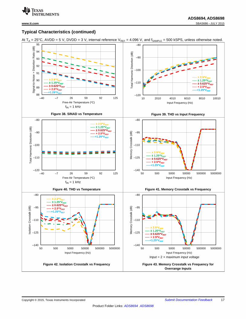
fIN = 1 kHz
Figure 38. SINAD vs Temperature Figure 39. THD vs Input Frequency
fIN = 1 kHz
Figure 40. THD vs Temperature Figure 41. Memory Crosstalk vs Frequency
Input = 2 × maximum input voltage
Figure 42. Isolation Crosstalk vs Frequency Figure 43. Memory Crosstalk vs Frequency forOverrange Inputs
Copyright © 2015, Texas Instruments Incorporated Submit Documentation Feedback 17
Product Folder Links: ADS8694 ADS8698
2
2.1
2.2
2.3
±40 ±7 26 59 92 125
I AV
DD S
tand
by (
mA
)
Free-Air Temperature (oC) C060
4.5
4.75
5
5.25
5.5
5.75
6
±40 ±7 26 59 92 125
I AV
DD S
tatic
(m
A)
Free-Air Temperature(oC) C063
7.5
7.75
8
8.25
8.5
8.75
9
±40 ±7 26 59 92 125
I AV
DD S
tatic
(m
A)
Free-Air Temperature (oC) C059
7.5
8
8.5
9
9.5
10
±40 ±7 26 59 92 125
I AV
DD D
ynam
ic (
mA
)
Free-Air Temperature (oC) C062
±140
±125
±110
±95
±80
100 1000 10000 100000 1000000 10000000
Isol
atio
n C
ross
talk
(dB
)
Input Frequency (Hz) C045
----- ± 2.5*VREF ----- � 1.25*VREF ----- � 0.625*VREF ----- + 2.5*VREF -----+1.25*VREF
10
10.5
11
11.5
12
±40 ±7 26 59 92 125
I AV
DD D
ynam
ic (
mA
)
Free-Air Temperature (oC) C058
ADS8694, ADS8698SBAS686 –JULY 2015 www.ti.com
Typical Characteristics (continued)At TA = 25°C, AVDD = 5 V, DVDD = 3 V, internal reference VREF = 4.096 V, and fSAMPLE = 500 kSPS, unless otherwise noted.
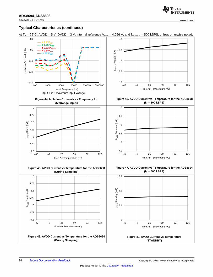
Input = 2 × maximum input voltage
Figure 45. AVDD Current vs Temperature for the ADS8698Figure 44. Isolation Crosstalk vs Frequency for(fS = 500 kSPS)Overrange Inputs
Figure 47. AVDD Current vs Temperature for the ADS8694Figure 46. AVDD Current vs Temperature for the ADS8698(fS = 500 kSPS)(During Sampling)
Figure 48. AVDD Current vs Temperature for the ADS8694 Figure 49. AVDD Current vs Temperature(During Sampling) (STANDBY)
18 Submit Documentation Feedback Copyright © 2015, Texas Instruments Incorporated
Product Folder Links: ADS8694 ADS8698
1
2
3
4
5
6
±40 ±7 26 59 92 125
I AV
DD P
D (
uA)
Free-Air Temperature (oC) C077
ADS8694, ADS8698www.ti.com SBAS686 –JULY 2015
Typical Characteristics (continued)At TA = 25°C, AVDD = 5 V, DVDD = 3 V, internal reference VREF = 4.096 V, and fSAMPLE = 500 kSPS, unless otherwise noted.
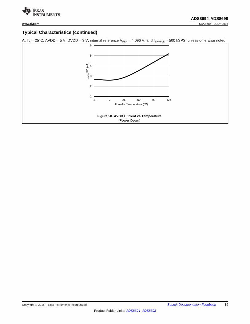
Figure 50. AVDD Current vs Temperature(Power Down)
Copyright © 2015, Texas Instruments Incorporated Submit Documentation Feedback 19
Product Folder Links: ADS8694 ADS8698
Mul
tiple
xer
Oscillator
PGA
1 M:
OVP
1 M:
2nd-OrderLPF
ADCDriver
VB0
AIN_0P
AIN_0GNDOVP
PGA
1 M:
OVP
1 M:
2nd-OrderLPF
ADCDriver
VB1
AIN_1P
AIN_1GNDOVP
PGA
1 M:
OVP
1 M:
2nd-OrderLPF
ADCDriver
VB2
AIN_2P
AIN_2GNDOVP
PGA
1 M:
OVP
1 M:
2nd-OrderLPF
ADCDriver
VB3
AIN_3P
AIN_3GNDOVP
PGA
1 M:
OVP
1 M:
2nd-OrderLPF
ADCDriver
VB4
AIN_4P
AIN_4GNDOVP
PGA
1 M:
OVP
1 M:
2nd-OrderLPF
ADCDriver
VB5
AIN_5P
AIN_5GNDOVP
PGA
1 M:
OVP
1 M:
2nd-OrderLPF
ADCDriver
VB6
AIN_6P
AIN_6GNDOVP
PGA
1 M:
OVP
1 M:
2nd-OrderLPF
ADCDriver
VB7
AIN_7P
AIN_7GNDOVP
AUX_IN
AUX_GND
18-BitSAR ADC
Digital Logic and
Interface
4.096-VReference
REFGNDDGNDAGND
DVDDAVDD
Add
ition
al C
hann
els
in A
DS
8698
ADS8698ADS8694
ALARM
CS
SCLK
SDI
SDO
DAISY
REFSEL
RST/PD
REFCAP
REFIO
Internal ADC operating as 16-bit
ADS8694, ADS8698SBAS686 –JULY 2015 www.ti.com
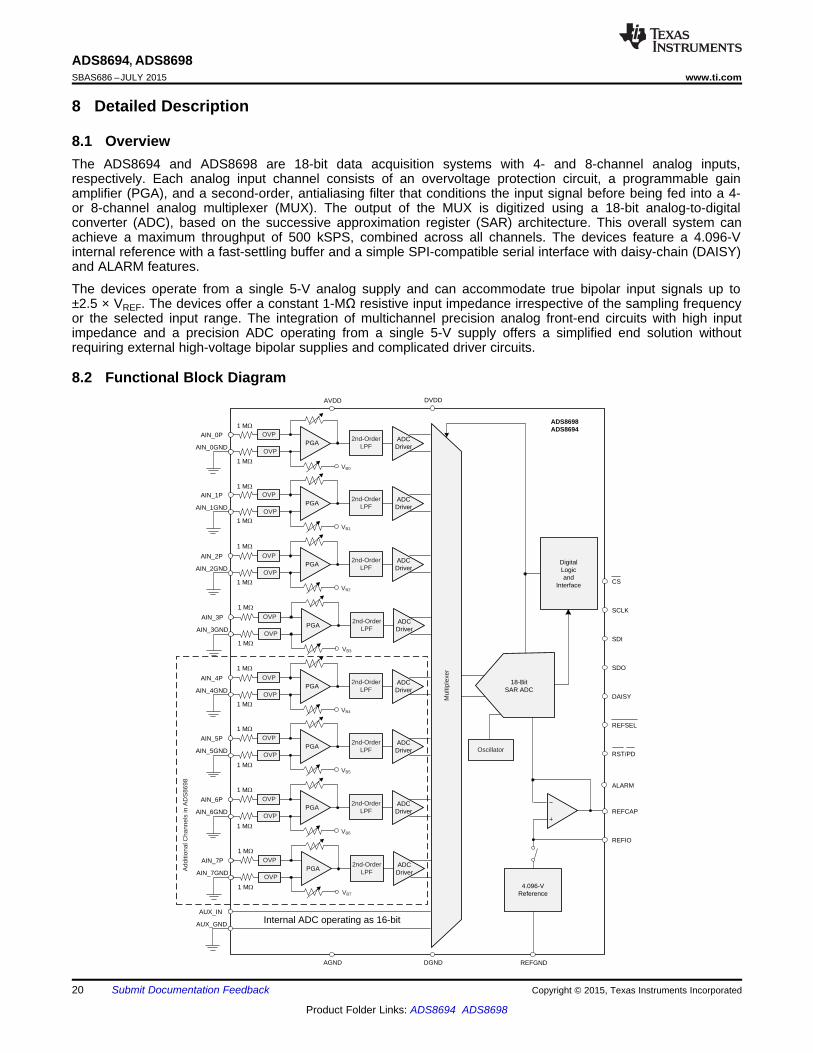
8 Detailed Description
8.1 OverviewThe ADS8694 and ADS8698 are 18-bit data acquisition systems with 4- and 8-channel analog inputs,respectively. Each analog input channel consists of an overvoltage protection circuit, a programmable gainamplifier (PGA), and a second-order, antialiasing filter that conditions the input signal before being fed into a 4-or 8-channel analog multiplexer (MUX). The output of the MUX is digitized using a 18-bit analog-to-digitalconverter (ADC), based on the successive approximation register (SAR) architecture. This overall system canachieve a maximum throughput of 500 kSPS, combined across all channels. The devices feature a 4.096-Vinternal reference with a fast-settling buffer and a simple SPI-compatible serial interface with daisy-chain (DAISY)and ALARM features.
The devices operate from a single 5-V analog supply and can accommodate true bipolar input signals up to±2.5 × VREF. The devices offer a constant 1-MΩ resistive input impedance irrespective of the sampling frequencyor the selected input range. The integration of multichannel precision analog front-end circuits with high inputimpedance and a precision ADC operating from a single 5-V supply offers a simplified end solution withoutrequiring external high-voltage bipolar supplies and complicated driver circuits.
8.2 Functional Block Diagram
20 Submit Documentation Feedback Copyright © 2015, Texas Instruments Incorporated
Product Folder Links: ADS8694 ADS8698
MUXPGA
1 M:
OVP
1 M:
OVP
2nd-OrderLPF
ADCDriver
VB
ADCAIN_nP
AIN_nGND
CSSCLKSDISDODAISY
ADS8694, ADS8698www.ti.com SBAS686 –JULY 2015
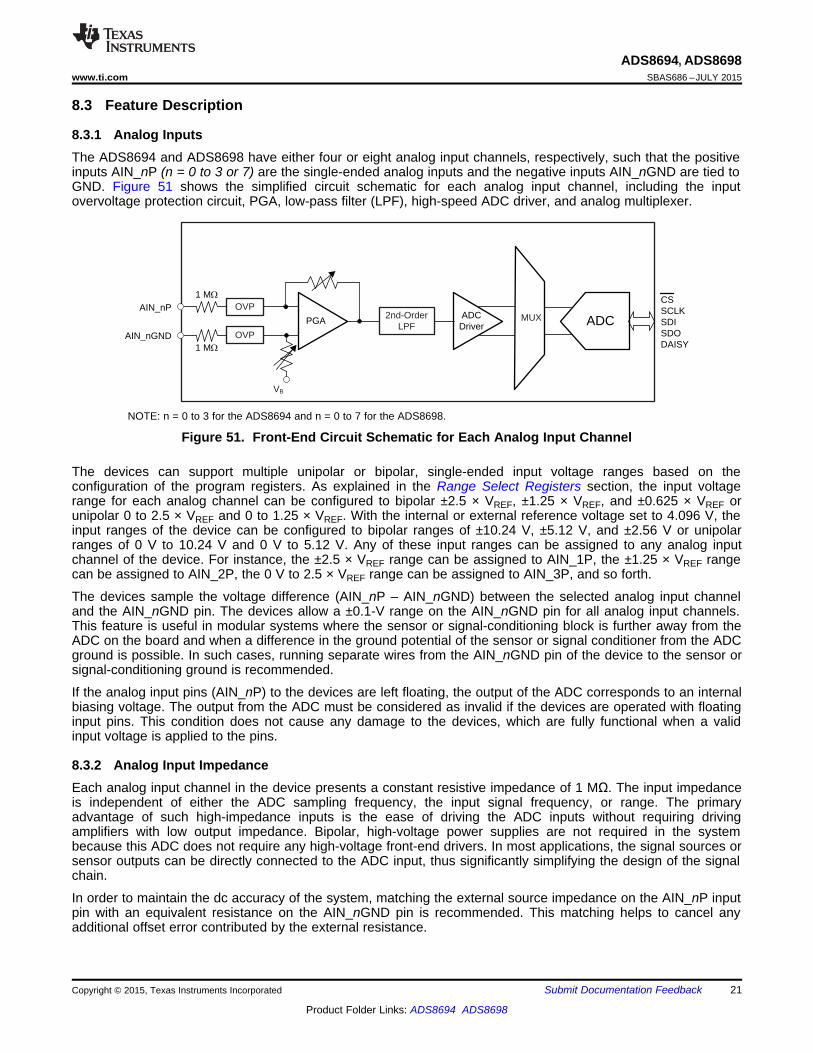
8.3 Feature Description
8.3.1 Analog InputsThe ADS8694 and ADS8698 have either four or eight analog input channels, respectively, such that the positiveinputs AIN_nP (n = 0 to 3 or 7) are the single-ended analog inputs and the negative inputs AIN_nGND are tied toGND. Figure 51 shows the simplified circuit schematic for each analog input channel, including the inputovervoltage protection circuit, PGA, low-pass filter (LPF), high-speed ADC driver, and analog multiplexer.
NOTE: n = 0 to 3 for the ADS8694 and n = 0 to 7 for the ADS8698.
Figure 51. Front-End Circuit Schematic for Each Analog Input Channel
The devices can support multiple unipolar or bipolar, single-ended input voltage ranges based on theconfiguration of the program registers. As explained in the Range Select Registers section, the input voltagerange for each analog channel can be configured to bipolar ±2.5 × VREF, ±1.25 × VREF, and ±0.625 × VREF orunipolar 0 to 2.5 × VREF and 0 to 1.25 × VREF. With the internal or external reference voltage set to 4.096 V, theinput ranges of the device can be configured to bipolar ranges of ±10.24 V, ±5.12 V, and ±2.56 V or unipolarranges of 0 V to 10.24 V and 0 V to 5.12 V. Any of these input ranges can be assigned to any analog inputchannel of the device. For instance, the ±2.5 × VREF range can be assigned to AIN_1P, the ±1.25 × VREF rangecan be assigned to AIN_2P, the 0 V to 2.5 × VREF range can be assigned to AIN_3P, and so forth.
The devices sample the voltage difference (AIN_nP – AIN_nGND) between the selected analog input channeland the AIN_nGND pin. The devices allow a ±0.1-V range on the AIN_nGND pin for all analog input channels.This feature is useful in modular systems where the sensor or signal-conditioning block is further away from theADC on the board and when a difference in the ground potential of the sensor or signal conditioner from the ADCground is possible. In such cases, running separate wires from the AIN_nGND pin of the device to the sensor orsignal-conditioning ground is recommended.
If the analog input pins (AIN_nP) to the devices are left floating, the output of the ADC corresponds to an internalbiasing voltage. The output from the ADC must be considered as invalid if the devices are operated with floatinginput pins. This condition does not cause any damage to the devices, which are fully functional when a validinput voltage is applied to the pins.
8.3.2 Analog Input ImpedanceEach analog input channel in the device presents a constant resistive impedance of 1 MΩ. The input impedanceis independent of either the ADC sampling frequency, the input signal frequency, or range. The primaryadvantage of such high-impedance inputs is the ease of driving the ADC inputs without requiring drivingamplifiers with low output impedance. Bipolar, high-voltage power supplies are not required in the systembecause this ADC does not require any high-voltage front-end drivers. In most applications, the signal sources orsensor outputs can be directly connected to the ADC input, thus significantly simplifying the design of the signalchain.
In order to maintain the dc accuracy of the system, matching the external source impedance on the AIN_nP inputpin with an equivalent resistance on the AIN_nGND pin is recommended. This matching helps to cancel anyadditional offset error contributed by the external resistance.
Copyright © 2015, Texas Instruments Incorporated Submit Documentation Feedback 21
Product Folder Links: ADS8694 ADS8698
VOUT
V+
V±
+
VB
AVDD
GND
AIN_nP
AIN_nGND
10��
10��
RDC
RFB0V
VP+
VP- RS
ESD
D1p
D2n
RS
AVDD
AVDDD2p
D1n
ESD
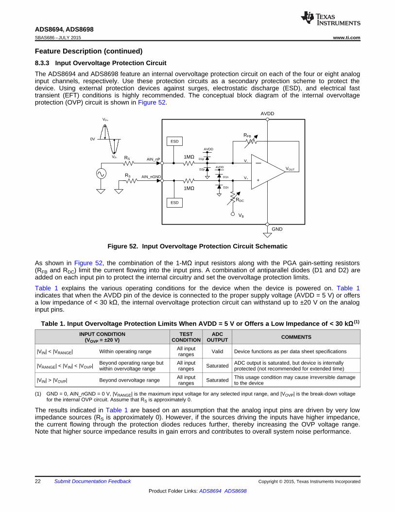
ADS8694, ADS8698SBAS686 –JULY 2015 www.ti.com
Feature Description (continued)8.3.3 Input Overvoltage Protection CircuitThe ADS8694 and ADS8698 feature an internal overvoltage protection circuit on each of the four or eight analoginput channels, respectively. Use these protection circuits as a secondary protection scheme to protect thedevice. Using external protection devices against surges, electrostatic discharge (ESD), and electrical fasttransient (EFT) conditions is highly recommended. The conceptual block diagram of the internal overvoltageprotection (OVP) circuit is shown in Figure 52.
Figure 52. Input Overvoltage Protection Circuit Schematic
As shown in Figure 52, the combination of the 1-MΩ input resistors along with the PGA gain-setting resistors(RFB and RDC) limit the current flowing into the input pins. A combination of antiparallel diodes (D1 and D2) areadded on each input pin to protect the internal circuitry and set the overvoltage protection limits.
Table 1 explains the various operating conditions for the device when the device is powered on. Table 1indicates that when the AVDD pin of the device is connected to the proper supply voltage (AVDD = 5 V) or offersa low impedance of < 30 kΩ, the internal overvoltage protection circuit can withstand up to ±20 V on the analoginput pins.
Table 1. Input Overvoltage Protection Limits When AVDD = 5 V or Offers a Low Impedance of < 30 kΩ (1)
INPUT CONDITION TEST ADC COMMENTS(VOVP = ±20 V) CONDITION OUTPUTAll input|VIN| < |VRANGE| Within operating range Valid Device functions as per data sheet specificationsranges
Beyond operating range but All input ADC output is saturated, but device is internally|VRANGE| < |VIN| < |VOVP| Saturatedwithin overvoltage range ranges protected (not recommended for extended time)All input This usage condition may cause irreversible damage|VIN| > |VOVP| Beyond overvoltage range Saturatedranges to the device
(1) GND = 0, AIN_nGND = 0 V, |VRANGE| is the maximum input voltage for any selected input range, and |VOVP| is the break-down voltagefor the internal OVP circuit. Assume that RS is approximately 0.
The results indicated in Table 1 are based on an assumption that the analog input pins are driven by very lowimpedance sources (RS is approximately 0). However, if the sources driving the inputs have higher impedance,the current flowing through the protection diodes reduces further, thereby increasing the OVP voltage range.Note that higher source impedance results in gain errors and contributes to overall system noise performance.
22 Submit Documentation Feedback Copyright © 2015, Texas Instruments Incorporated
Product Folder Links: ADS8694 ADS8698
±20
±12
±4
4
12
20
±20 ±12 ±4 4 12 20
Ana
log
Inpu
t Cur
rent
(µ
A)
Input Voltage (V) C004
±30
±20
±10
0
10
20
30
±30 ±20 ±10 0 10 20 30
Ana
log
Inpu
t Cur
rent
(µ
A)
Input Voltage (V) C003
----- ± 2.5 VREF ----- ± 1.25 VREF ----- ± 0.625 VREF ------ +2.5 VREF ------+1.25VREF
ADS8694, ADS8698www.ti.com SBAS686 –JULY 2015
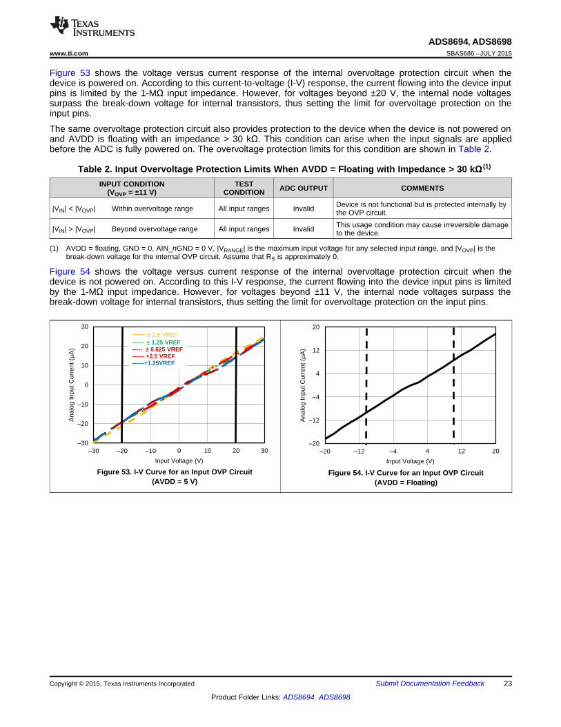
Figure 53 shows the voltage versus current response of the internal overvoltage protection circuit when thedevice is powered on. According to this current-to-voltage (I-V) response, the current flowing into the device inputpins is limited by the 1-MΩ input impedance. However, for voltages beyond ±20 V, the internal node voltagessurpass the break-down voltage for internal transistors, thus setting the limit for overvoltage protection on theinput pins.
The same overvoltage protection circuit also provides protection to the device when the device is not powered onand AVDD is floating with an impedance > 30 kΩ. This condition can arise when the input signals are appliedbefore the ADC is fully powered on. The overvoltage protection limits for this condition are shown in Table 2.
Table 2. Input Overvoltage Protection Limits When AVDD = Floating with Impedance > 30 kΩ (1)
INPUT CONDITION TEST ADC OUTPUT COMMENTS(VOVP = ±11 V) CONDITIONDevice is not functional but is protected internally by|VIN| < |VOVP| Within overvoltage range All input ranges Invalid the OVP circuit.This usage condition may cause irreversible damage|VIN| > |VOVP| Beyond overvoltage range All input ranges Invalid to the device.
(1) AVDD = floating, GND = 0, AIN_nGND = 0 V, |VRANGE| is the maximum input voltage for any selected input range, and |VOVP| is thebreak-down voltage for the internal OVP circuit. Assume that RS is approximately 0.
Figure 54 shows the voltage versus current response of the internal overvoltage protection circuit when thedevice is not powered on. According to this I-V response, the current flowing into the device input pins is limitedby the 1-MΩ input impedance. However, for voltages beyond ±11 V, the internal node voltages surpass thebreak-down voltage for internal transistors, thus setting the limit for overvoltage protection on the input pins.
Figure 53. I-V Curve for an Input OVP Circuit Figure 54. I-V Curve for an Input OVP Circuit(AVDD = 5 V) (AVDD = Floating)
Copyright © 2015, Texas Instruments Incorporated Submit Documentation Feedback 23
Product Folder Links: ADS8694 ADS8698
±6
±5
±4
±3
±2
±1
0
100 1000 10000
Mag
nitu
de (
dB)
Input Frequency (Hz) C048
----- ± 2.5*VREF ----- � 1.25*VREF ----- � 0.625*VREF ----- + 2.5*VREF -----+1.25*VREF
±90
±75
±60
±45
±30
±15
0
100 1000 10000
Pha
se (
Deg
ree)
Input Frequency (Hz) C049
----- ± 2.5*VREF ----- � 1.25*VREF ----- � 0.625*VREF ----- + 2.5*VREF -----+1.25*VREF
ADS8694, ADS8698SBAS686 –JULY 2015 www.ti.com
8.3.4 Programmable Gain Amplifier (PGA)The devices offer a programmable gain amplifier (PGA) at each individual analog input channel, which convertsthe original single-ended input signal into a fully-differential signal to drive the internal 18-bit ADC. The PGA alsoadjusts the common-mode level of the input signal before being fed into the ADC to ensure maximum usage ofthe ADC input dynamic range. Depending on the range of the input signal, the PGA gain can be accordinglyadjusted by setting the Range_CHn[3:0] (n = 0 to 3 or 7) bits in the program register. The default or power-onstate for the Range_CHn[3:0] bits is 0000, which corresponds to an input signal range of ±2.5 × VREF. Table 3lists the various configurations of the Range_CHn[3:0] bits for the different analog input voltage ranges.
The PGA uses a very highly-matched network of resistors for multiple gain configurations. Matching betweenthese resistors and the amplifiers across all channels is accurately trimmed to keep the overall gain error lowacross all channels and input ranges.
Table 3. Input Range Selection Bits ConfigurationRange_CHn[3:0]
ANALOG INPUT RANGEBIT 3 BIT 2 BIT 1 BIT 0
±2.5 × VREF 0 0 0 0±1.25 × VREF 0 0 0 1±0.625 × VREF 0 0 1 00 to 2.5 × VREF 0 1 0 10 to 1.25 × VREF 0 1 1 0
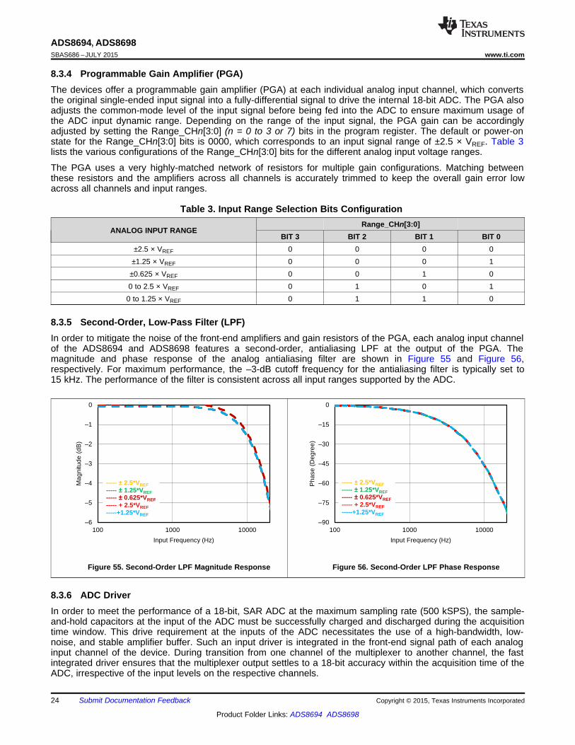
8.3.5 Second-Order, Low-Pass Filter (LPF)In order to mitigate the noise of the front-end amplifiers and gain resistors of the PGA, each analog input channelof the ADS8694 and ADS8698 features a second-order, antialiasing LPF at the output of the PGA. Themagnitude and phase response of the analog antialiasing filter are shown in Figure 55 and Figure 56,respectively. For maximum performance, the –3-dB cutoff frequency for the antialiasing filter is typically set to15 kHz. The performance of the filter is consistent across all input ranges supported by the ADC.
Figure 55. Second-Order LPF Magnitude Response Figure 56. Second-Order LPF Phase Response
8.3.6 ADC DriverIn order to meet the performance of a 18-bit, SAR ADC at the maximum sampling rate (500 kSPS), the sample-and-hold capacitors at the input of the ADC must be successfully charged and discharged during the acquisitiontime window. This drive requirement at the inputs of the ADC necessitates the use of a high-bandwidth, low-noise, and stable amplifier buffer. Such an input driver is integrated in the front-end signal path of each analoginput channel of the device. During transition from one channel of the multiplexer to another channel, the fastintegrated driver ensures that the multiplexer output settles to a 18-bit accuracy within the acquisition time of theADC, irrespective of the input levels on the respective channels.
24 Submit Documentation Feedback Copyright © 2015, Texas Instruments Incorporated
Product Folder Links: ADS8694 ADS8698
ADS8694, ADS8698www.ti.com SBAS686 –JULY 2015
8.3.7 Multiplexer (MUX)The ADS8694 and ADS8698 feature an integrated 4- and 8-channel analog multiplexer, respectively. For eachanalog input channel, the voltage difference between the positive analog input AIN_nP and the negative groundinput AIN_nGND is conditioned by the analog front-end circuitry before being fed into the multiplexer. The outputof the multiplexer is directly sampled by the ADC. The multiplexer in the device can scan these analog inputs ineither manual or auto-scan mode, as explained in the Channel Sequencing Modes section. In manual mode(MAN_Ch_n), the channel is selected for every sample via a register write; in auto-scan mode (AUTO_RST), thechannel number is incremented automatically on every CS falling edge after the present channel is sampled. Theanalog inputs can be selected for an auto scan with register settings (see the Auto-Scan Sequencing ControlRegisters section). The devices automatically scan only the selected analog inputs in ascending order.
The maximum overall throughput for the ADS8694 and ADS8698 is specified at 500 kSPS across all channels.The per channel throughput is dependent on the number of channels selected in the multiplexer scanningsequence. For example, the throughput per channel is equal to 250 kSPS if only two channels are selected, butis equal to 125 kSPS per channel if four channels are selected (as in the ADS8694), and so forth.
See Table 6 for command register settings to switch between the auto-scan mode and manual mode forindividual analog channels.
8.3.8 ReferenceThe ADS8694 and ADS8698 can operate with either an internal voltage reference or an external voltagereference using the internal buffer. The internal or external reference selection is determined by an externalREFSEL pin. The devices have a built-in buffer amplifier to drive the actual reference input of the internal ADCcore for maximizing performance.
Copyright © 2015, Texas Instruments Incorporated Submit Documentation Feedback 25
Product Folder Links: ADS8694 ADS8698
0
100
200
300
400
500
600
-1 -0.6 -0.2 0.2 0.6 1
Num
ber
of D
evic
es
Error in REFIO Voltage (mV) C064
ADC
4.096 VREF
REFCAP
REFIO
AGND
22 PF
REFGND
10 PF
REFSEL
AVDD
1 PF
ADS8694, ADS8698SBAS686 –JULY 2015 www.ti.com
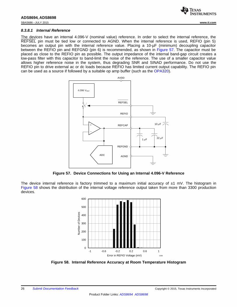
8.3.8.1 Internal ReferenceThe devices have an internal 4.096-V (nominal value) reference. In order to select the internal reference, theREFSEL pin must be tied low or connected to AGND. When the internal reference is used, REFIO (pin 5)becomes an output pin with the internal reference value. Placing a 10-µF (minimum) decoupling capacitorbetween the REFIO pin and REFGND (pin 6) is recommended, as shown in Figure 57. The capacitor must beplaced as close to the REFIO pin as possible. The output impedance of the internal band-gap circuit creates alow-pass filter with this capacitor to band-limit the noise of the reference. The use of a smaller capacitor valueallows higher reference noise in the system, thus degrading SNR and SINAD performance. Do not use theREFIO pin to drive external ac or dc loads because REFIO has limited current output capability. The REFIO pincan be used as a source if followed by a suitable op amp buffer (such as the OPA320).
Figure 57. Device Connections for Using an Internal 4.096-V Reference
The device internal reference is factory trimmed to a maximum initial accuracy of ±1 mV. The histogram inFigure 58 shows the distribution of the internal voltage reference output taken from more than 3300 productiondevices.
Figure 58. Internal Reference Accuracy at Room Temperature Histogram
26 Submit Documentation Feedback Copyright © 2015, Texas Instruments Incorporated
Product Folder Links: ADS8694 ADS8698
4.09
4.091
4.092
4.093
4.094
4.095
4.096
4.097
4.098
4.099
4.1
±40 ±7 26 59 92 125
RE
FIO
Vol
tage
(V
)
Free-Air Temperature (oC) C053
----- AVDD = 5.25 V ------ AVDD = 5 V ------ AVDD = 4.75 V
0
4
8
12
16
20
1 2 3 4 5 6 7 8 9 10
Num
ber
of D
evic
es
REFIO Drift (ppm/ºC) C054
0
5
10
15
20
25
30
-4 -3 -2 -1 0 1
Num
ber
of D
evic
es
Error in REFIO Voltage (mV) C065
ADS8694, ADS8698www.ti.com SBAS686 –JULY 2015
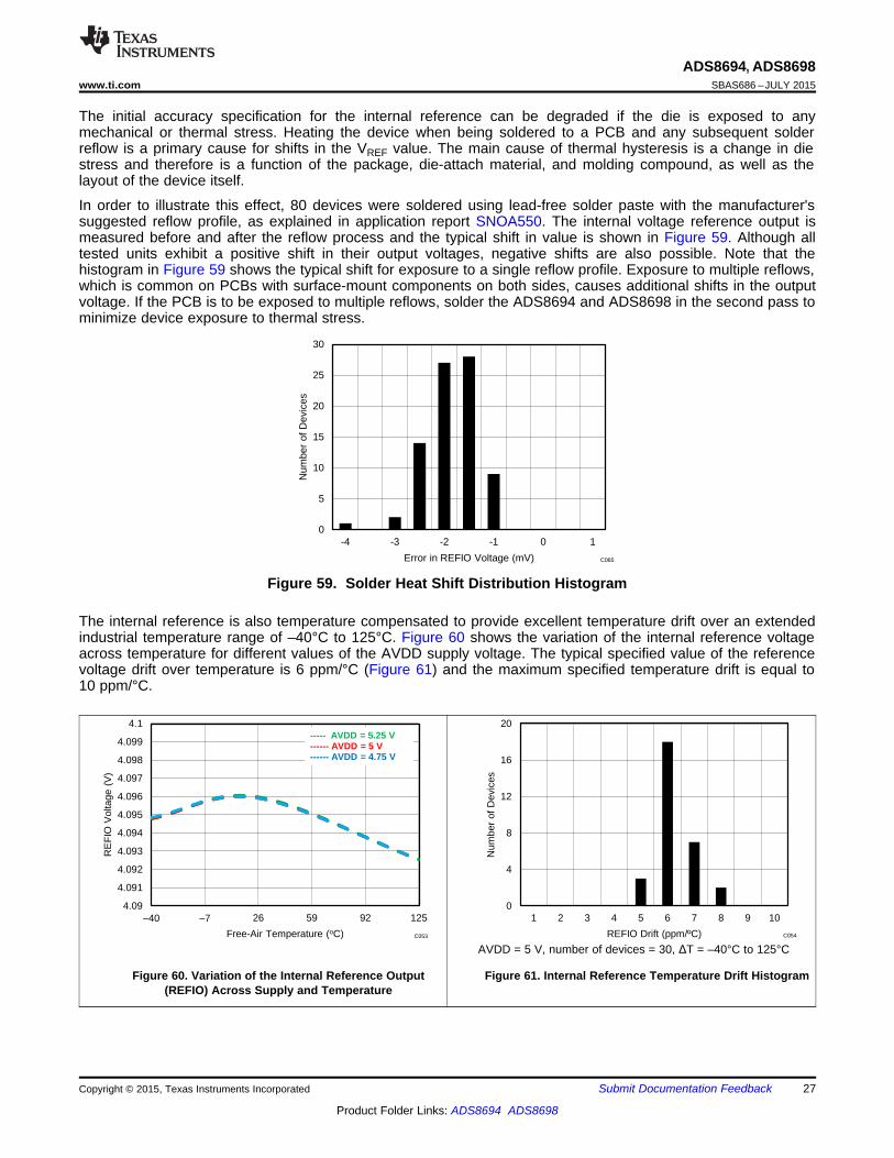
The initial accuracy specification for the internal reference can be degraded if the die is exposed to anymechanical or thermal stress. Heating the device when being soldered to a PCB and any subsequent solderreflow is a primary cause for shifts in the VREF value. The main cause of thermal hysteresis is a change in diestress and therefore is a function of the package, die-attach material, and molding compound, as well as thelayout of the device itself.
In order to illustrate this effect, 80 devices were soldered using lead-free solder paste with the manufacturer'ssuggested reflow profile, as explained in application report SNOA550. The internal voltage reference output ismeasured before and after the reflow process and the typical shift in value is shown in Figure 59. Although alltested units exhibit a positive shift in their output voltages, negative shifts are also possible. Note that thehistogram in Figure 59 shows the typical shift for exposure to a single reflow profile. Exposure to multiple reflows,which is common on PCBs with surface-mount components on both sides, causes additional shifts in the outputvoltage. If the PCB is to be exposed to multiple reflows, solder the ADS8694 and ADS8698 in the second pass tominimize device exposure to thermal stress.
Figure 59. Solder Heat Shift Distribution Histogram
The internal reference is also temperature compensated to provide excellent temperature drift over an extendedindustrial temperature range of –40°C to 125°C. Figure 60 shows the variation of the internal reference voltageacross temperature for different values of the AVDD supply voltage. The typical specified value of the referencevoltage drift over temperature is 6 ppm/°C (Figure 61) and the maximum specified temperature drift is equal to10 ppm/°C.
AVDD = 5 V, number of devices = 30, ΔT = –40°C to 125°C
Figure 60. Variation of the Internal Reference Output Figure 61. Internal Reference Temperature Drift Histogram(REFIO) Across Supply and Temperature
Copyright © 2015, Texas Instruments Incorporated Submit Documentation Feedback 27
Product Folder Links: ADS8694 ADS8698
ADC
4.096 VREF
REFCAP
REFIO
AGND
22 PF
REFGND
CREF
REFSEL
AVDD
REF5040(See the device datasheet for a detailed pin configuration.)
AVDD
OUT
DVDD
1 PF
ADS8694, ADS8698SBAS686 –JULY 2015 www.ti.com
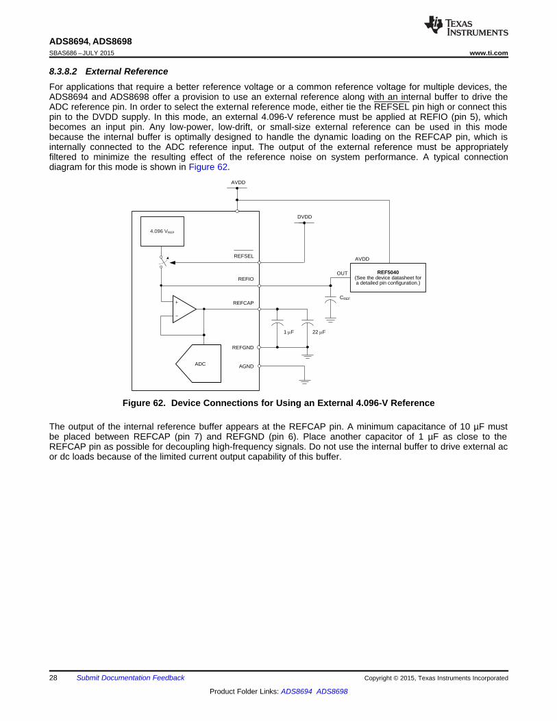
8.3.8.2 External ReferenceFor applications that require a better reference voltage or a common reference voltage for multiple devices, theADS8694 and ADS8698 offer a provision to use an external reference along with an internal buffer to drive theADC reference pin. In order to select the external reference mode, either tie the REFSEL pin high or connect thispin to the DVDD supply. In this mode, an external 4.096-V reference must be applied at REFIO (pin 5), whichbecomes an input pin. Any low-power, low-drift, or small-size external reference can be used in this modebecause the internal buffer is optimally designed to handle the dynamic loading on the REFCAP pin, which isinternally connected to the ADC reference input. The output of the external reference must be appropriatelyfiltered to minimize the resulting effect of the reference noise on system performance. A typical connectiondiagram for this mode is shown in Figure 62.
Figure 62. Device Connections for Using an External 4.096-V Reference
The output of the internal reference buffer appears at the REFCAP pin. A minimum capacitance of 10 µF mustbe placed between REFCAP (pin 7) and REFGND (pin 6). Place another capacitor of 1 µF as close to theREFCAP pin as possible for decoupling high-frequency signals. Do not use the internal buffer to drive external acor dc loads because of the limited current output capability of this buffer.
28 Submit Documentation Feedback Copyright © 2015, Texas Instruments Incorporated
Product Folder Links: ADS8694 ADS8698
4.095
4.0952
4.0954
4.0956
4.0958
4.096
4.0962
4.0964
4.0966
4.0968
4.097
±40 ±7 26 59 92 125
RE
FC
AP
Vol
tage
(V
)
Free-Air Temperature (oC) C055
----- AVDD = 5.25 V ------ AVDD = 5 V ------ AVDD = 4.75 V
0
3
6
9
12
15
0 0.2 0.4 0.6 0.8 1 1.2
Num
ber
of D
evic
es
REFCAP Drift (ppm/ºC) C056
ADS8694, ADS8698www.ti.com SBAS686 –JULY 2015
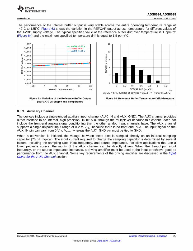
The performance of the internal buffer output is very stable across the entire operating temperature range of–40°C to 125°C. Figure 63 shows the variation in the REFCAP output across temperature for different values ofthe AVDD supply voltage. The typical specified value of the reference buffer drift over temperature is 1 ppm/°C(Figure 64) and the maximum specified temperature drift is equal to 1.5 ppm/°C.
AVDD = 5 V, number of devices = 30, ΔT = –40°C to 125°C
Figure 63. Variation of the Reference Buffer Output Figure 64. Reference Buffer Temperature Drift Histogram(REFCAP) vs Supply and Temperature
8.3.9 Auxiliary ChannelThe devices include a single-ended auxiliary input channel (AUX_IN and AUX_GND). The AUX channel providesdirect interface to an internal, high-precision, 16-bit ADC through the multiplexer because this channel does notinclude the front-end analog signal conditioning that the other analog input channels have. The AUX channelsupports a single unipolar input range of 0 V to VREF because there is no front-end PGA. The input signal on theAUX_IN pin can vary from 0 V to VREF, whereas the AUX_GND pin must be tied to GND.
When a conversion is initiated, the voltage between these pins is sampled directly on an internal samplingcapacitor (75 pF, typical). The input current required to charge the sampling capacitor is determined by severalfactors, including the sampling rate, input frequency, and source impedance. For slow applications that use alow-impedance source, the inputs of the AUX channel can be directly driven. When the throughput, inputfrequency, or the source impedance increases, a driving amplifier must be used at the input to achieve good acperformance from the AUX channel. Some key requirements of the driving amplifier are discussed in the InputDriver for the AUX Channel section.
Copyright © 2015, Texas Instruments Incorporated Submit Documentation Feedback 29
Product Folder Links: ADS8694 ADS8698
±160
±140
±120
±100
±80
±60
±40
±20
0
0 50000 100000 150000 200000 250000
Am
plitu
de
Input Frequency (Hz) C052
-105
-104
-103
-102
-101
-100
86
87
88
89
90
-40 -7 26 59 92 125
SN
R, S
INA
D (
dB)
Free-Air Temperature (oC) C053
SNR
THD
SINAD
TH
D (dB
)
0
0.1
0.2
0.3
0.4
0.5
-0.2
-0.15
-0.1
-0.05
0
0.05
0.1
0.15
0.2
-40 -7 26 59 92 125
Offs
et E
rror
(m
V)
Gai
n E
rror
(%
FS
)
Free-Air temperature (oC) C051
Offset Error
Gain Error
0
2000
4000
6000
8000
32763 32764 32765 32766 32767 32768 32769 32770 32771
Num
ber
of H
its
Codes (LSB) C050
ADS8694, ADS8698SBAS686 –JULY 2015 www.ti.com
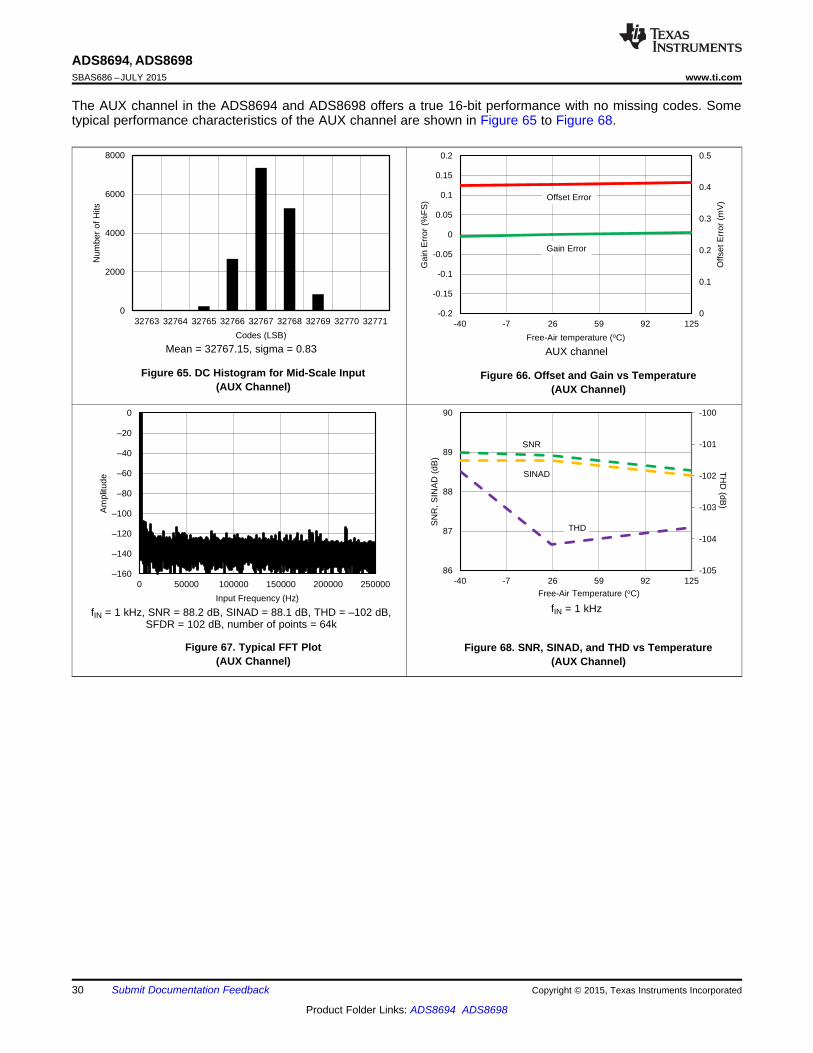
The AUX channel in the ADS8694 and ADS8698 offers a true 16-bit performance with no missing codes. Sometypical performance characteristics of the AUX channel are shown in Figure 65 to Figure 68.
Mean = 32767.15, sigma = 0.83 AUX channel
Figure 65. DC Histogram for Mid-Scale Input Figure 66. Offset and Gain vs Temperature(AUX Channel) (AUX Channel)
fIN = 1 kHzfIN = 1 kHz, SNR = 88.2 dB, SINAD = 88.1 dB, THD = –102 dB,SFDR = 102 dB, number of points = 64k
Figure 67. Typical FFT Plot Figure 68. SNR, SINAD, and THD vs Temperature(AUX Channel) (AUX Channel)
30 Submit Documentation Feedback Copyright © 2015, Texas Instruments Incorporated
Product Folder Links: ADS8694 ADS8698
� �_ _
_.
2 SNR dB1 AMP PP 2 FSRf 20
G n RMS 3dB
V V1N e f 10
6 6 2 5 2 2
S �
�
§ ·¨ ¸u � u u d u u¨ ¸© ¹
� �AMP ADCTHD THD 10 dBd �
3 dBGBW 4 f�
t u
ADS8694, ADS8698www.ti.com SBAS686 –JULY 2015
8.3.9.1 Input Driver for the AUX ChannelFor applications that use the AUX input channels at high throughput and high input frequency, a driving amplifierwith low output impedance is required to meet the ac performance of the internal 16-bit ADC. Some keyspecifications of the input driving amplifier are discussed below:• Small-signal bandwidth. The small-signal bandwidth of the input driving amplifier must be much higher than
the bandwidth of the AUX input to ensure that there is no attenuation of the input signal resulting from thebandwidth limitation of the amplifier. In a typical data acquisition system, a low cut-off frequency, antialiasingfilter is used at the inputs of a high-resolution ADC. The amplifier driving the antialiasing filter must have a lowclosed-loop output impedance for stability, thus implying a higher gain bandwidth for the amplifier. Highersmall-signal bandwidth also minimizes the harmonic distortion at higher input frequencies. In general, theamplifier bandwidth requirements can be calculated on the basis of Equation 1.
where:• f–3dB is the 3-dB bandwidth of the RC filter. (1)
• Distortion. In order to achieve the distortion performance of the AUX channel, the distortion of the input drivermust be at least 10 dB lower than the specified distortion of the internal ADC, as shown in Equation 2.
(2)• Noise. Careful considerations must be made to select a low-noise, front-end amplifier in order to prevent any
degradation in SNR performance of the system. As a rule of thumb, to ensure that the noise performance ofthe data acquisition system is not limited by the front-end circuit, keep the total noise contribution from thefront-end circuit below 20% of the input-referred noise of the ADC. Noise from the input driver circuit is band-limited by the low cut-off frequency of the input antialiasing filter, as explained in Equation 3.
where:• V1 / f_AMP_PP is the peak-to-peak flicker noise,• en_RMS is the amplifier broadband noise density in nV/√Hz, and• NG is the noise gain of the front-end circuit, which is equal to 1 in a buffer configuration. (3)
Copyright © 2015, Texas Instruments Incorporated Submit Documentation Feedback 31
Product Folder Links: ADS8694 ADS8698
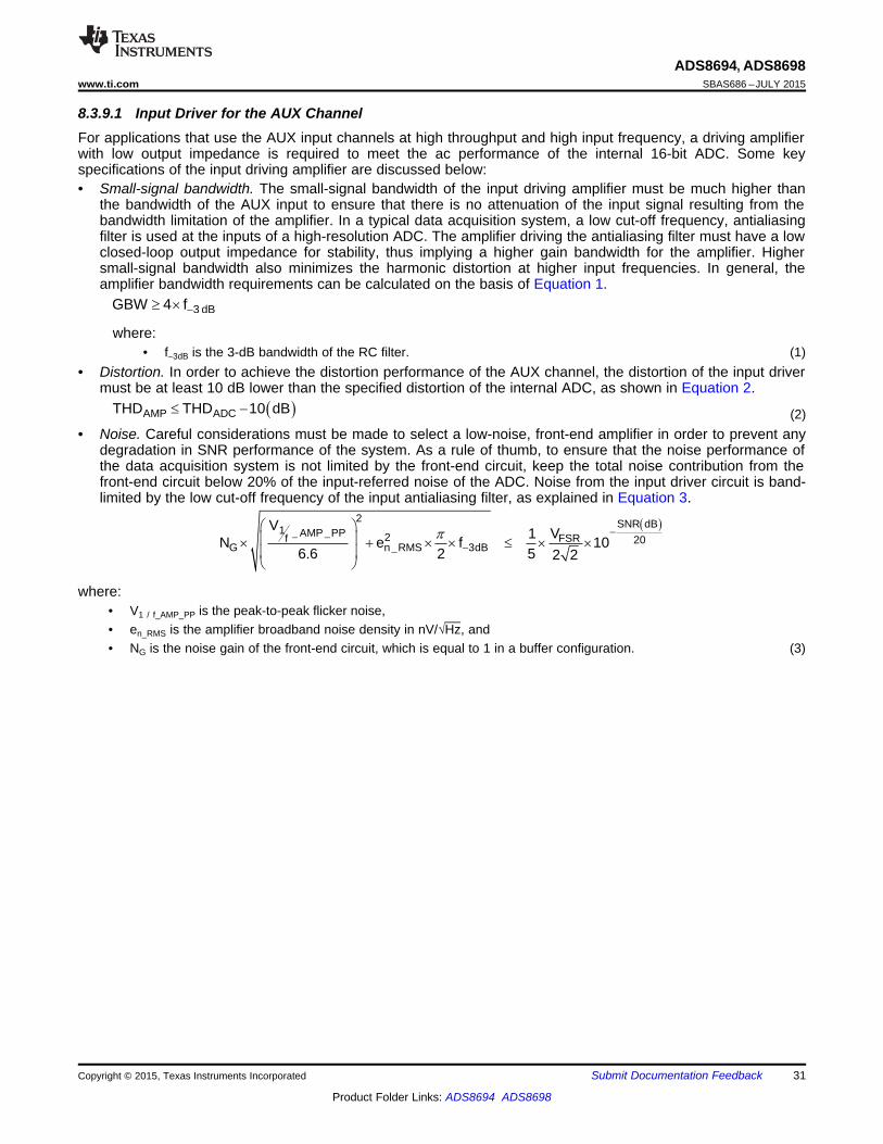
00001h
3FFFFh
20000h
FSR ± 1LSBFSR/21LSB
AD
C O
utpu
t Cod
e
Analog Input (AIN_nP t AIN_nGND)
NFS PFS
ADS8694, ADS8698SBAS686 –JULY 2015 www.ti.com
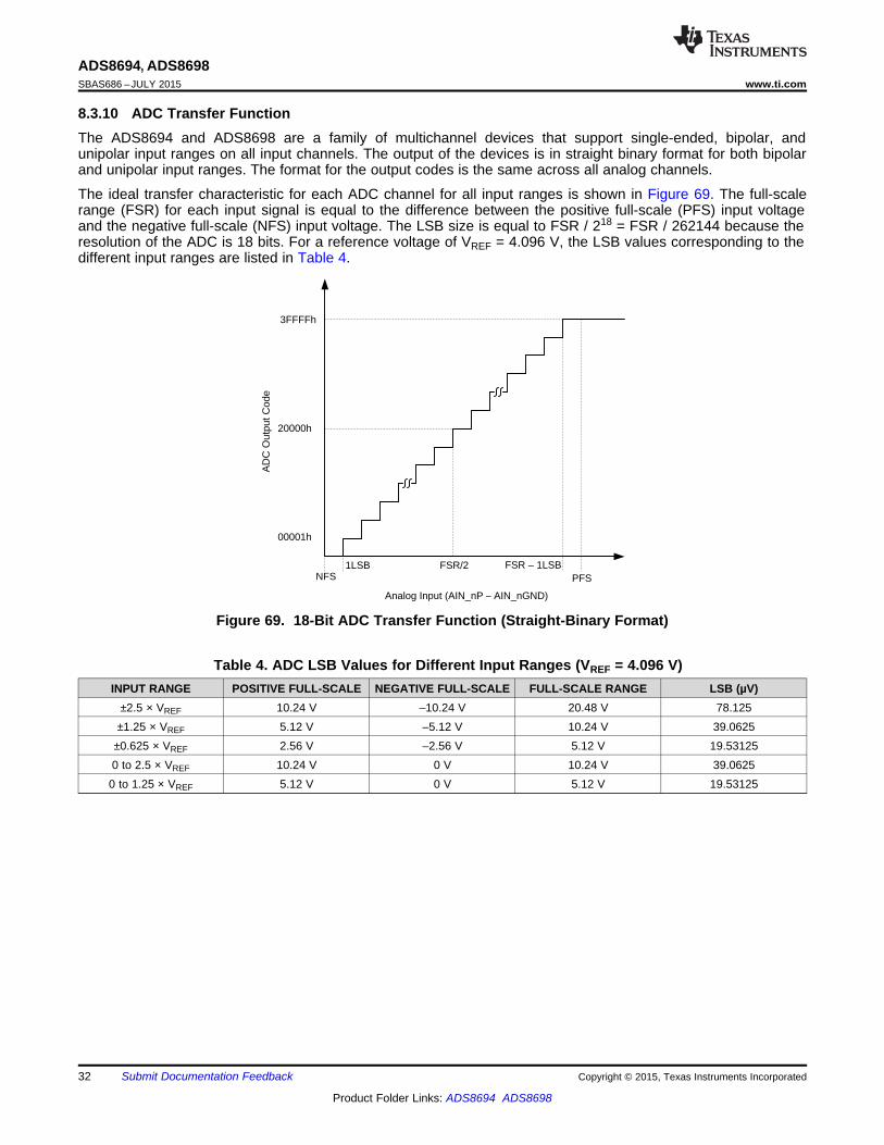
8.3.10 ADC Transfer FunctionThe ADS8694 and ADS8698 are a family of multichannel devices that support single-ended, bipolar, andunipolar input ranges on all input channels. The output of the devices is in straight binary format for both bipolarand unipolar input ranges. The format for the output codes is the same across all analog channels.
The ideal transfer characteristic for each ADC channel for all input ranges is shown in Figure 69. The full-scalerange (FSR) for each input signal is equal to the difference between the positive full-scale (PFS) input voltageand the negative full-scale (NFS) input voltage. The LSB size is equal to FSR / 218 = FSR / 262144 because theresolution of the ADC is 18 bits. For a reference voltage of VREF = 4.096 V, the LSB values corresponding to thedifferent input ranges are listed in Table 4.
Figure 69. 18-Bit ADC Transfer Function (Straight-Binary Format)
Table 4. ADC LSB Values for Different Input Ranges (VREF = 4.096 V)INPUT RANGE POSITIVE FULL-SCALE NEGATIVE FULL-SCALE FULL-SCALE RANGE LSB (µV)
±2.5 × VREF 10.24 V –10.24 V 20.48 V 78.125±1.25 × VREF 5.12 V –5.12 V 10.24 V 39.0625
±0.625 × VREF 2.56 V –2.56 V 5.12 V 19.531250 to 2.5 × VREF 10.24 V 0 V 10.24 V 39.06250 to 1.25 × VREF 5.12 V 0 V 5.12 V 19.53125
32 Submit Documentation Feedback Copyright © 2015, Texas Instruments Incorporated
Product Folder Links: ADS8694 ADS8698
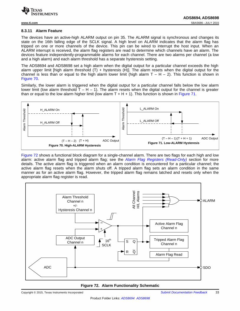
ADC OutputChannel n
Alarm Threshold Channel n
+/-Hysteresis Channel n
+
S Q
QRAlarm Flag Read
Active Alarm Flag Channel n
Tripped Alarm Flag Channel n
All
Cha
nnel
H
/L A
larm
s
SDO
ALARM
ADC
16th
SCLK
Ala
rm T
hres
hold
ADC Output
H_ALARM On
H_ALARM Off
(T ± H ± 2) (T + H)ADC Output
L_ALARM Off
L_ALARM On
(T + H + 1)(T ± H ± 1)
Ala
rm T
hres
hold
ADS8694, ADS8698www.ti.com SBAS686 –JULY 2015
8.3.11 Alarm FeatureThe devices have an active-high ALARM output on pin 35. The ALARM signal is synchronous and changes itsstate on the 16th falling edge of the SCLK signal. A high level on ALARM indicates that the alarm flag hastripped on one or more channels of the device. This pin can be wired to interrupt the host input. When anALARM interrupt is received, the alarm flag registers are read to determine which channels have an alarm. Thedevices feature independently-programmable alarms for each channel. There are two alarms per channel (a lowand a high alarm) and each alarm threshold has a separate hysteresis setting.
The ADS8694 and ADS8698 set a high alarm when the digital output for a particular channel exceeds the highalarm upper limit [high alarm threshold (T) + hysteresis (H)]. The alarm resets when the digital output for thechannel is less than or equal to the high alarm lower limit (high alarm T – H – 2). This function is shown inFigure 70.
Similarly, the lower alarm is triggered when the digital output for a particular channel falls below the low alarmlower limit (low alarm threshold T – H – 1). The alarm resets when the digital output for the channel is greaterthan or equal to the low alarm higher limit (low alarm T + H + 1). This function is shown in Figure 71.
Figure 71. Low-ALARM HysteresisFigure 70. High-ALARM Hysteresis
Figure 72 shows a functional block diagram for a single-channel alarm. There are two flags for each high and lowalarm: active alarm flag and tripped alarm flag; see the Alarm Flag Registers (Read-Only) section for moredetails. The active alarm flag is triggered when an alarm condition is encountered for a particular channel; theactive alarm flag resets when the alarm shuts off. A tripped alarm flag sets an alarm condition in the samemanner as for an active alarm flag. However, the tripped alarm flag remains latched and resets only when theappropriate alarm flag register is read.
Figure 72. Alarm Functionality SchematicCopyright © 2015, Texas Instruments Incorporated Submit Documentation Feedback 33
Product Folder Links: ADS8694 ADS8698
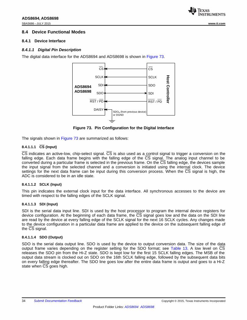
CS
SCLK
SDI
SDO
DAISY
ADS8694ADS8698
CS
SCLK
SDO
SDI
Ho
st Co
ntro
llerRST / PD RST / PD
SDON (from previous device) or DGND
ADS8694, ADS8698SBAS686 –JULY 2015 www.ti.com
8.4 Device Functional Modes
8.4.1 Device Interface
8.4.1.1 Digital Pin DescriptionThe digital data interface for the ADS8694 and ADS8698 is shown in Figure 73.
Figure 73. Pin Configuration for the Digital Interface
The signals shown in Figure 73 are summarized as follows:
8.4.1.1.1 CS (Input)
CS indicates an active-low, chip-select signal. CS is also used as a control signal to trigger a conversion on thefalling edge. Each data frame begins with the falling edge of the CS signal. The analog input channel to beconverted during a particular frame is selected in the previous frame. On the CS falling edge, the devices samplethe input signal from the selected channel and a conversion is initiated using the internal clock. The devicesettings for the next data frame can be input during this conversion process. When the CS signal is high, theADC is considered to be in an idle state.
8.4.1.1.2 SCLK (Input)
This pin indicates the external clock input for the data interface. All synchronous accesses to the device aretimed with respect to the falling edges of the SCLK signal.
8.4.1.1.3 SDI (Input)
SDI is the serial data input line. SDI is used by the host processor to program the internal device registers fordevice configuration. At the beginning of each data frame, the CS signal goes low and the data on the SDI lineare read by the device at every falling edge of the SCLK signal for the next 16 SCLK cycles. Any changes madeto the device configuration in a particular data frame are applied to the device on the subsequent falling edge ofthe CS signal.
8.4.1.1.4 SDO (Output)
SDO is the serial data output line. SDO is used by the device to output conversion data. The size of the dataoutput frame varies depending on the register setting for the SDO format; see Table 13. A low level on CSreleases the SDO pin from the Hi-Z state. SDO is kept low for the first 15 SCLK falling edges. The MSB of theoutput data stream is clocked out on SDO on the 16th SCLK falling edge, followed by the subsequent data bitson every falling edge thereafter. The SDO line goes low after the entire data frame is output and goes to a Hi-Zstate when CS goes high.
34 Submit Documentation Feedback Copyright © 2015, Texas Instruments Incorporated
Product Folder Links: ADS8694 ADS8698
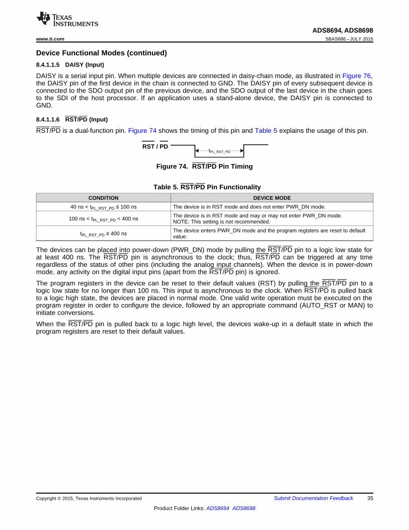
RST / PDtPL_RST_PD
ADS8694, ADS8698www.ti.com SBAS686 –JULY 2015
Device Functional Modes (continued)8.4.1.1.5 DAISY (Input)
DAISY is a serial input pin. When multiple devices are connected in daisy-chain mode, as illustrated in Figure 76,the DAISY pin of the first device in the chain is connected to GND. The DAISY pin of every subsequent device isconnected to the SDO output pin of the previous device, and the SDO output of the last device in the chain goesto the SDI of the host processor. If an application uses a stand-alone device, the DAISY pin is connected toGND.
8.4.1.1.6 RST/PD (Input)
RST/PD is a dual-function pin. Figure 74 shows the timing of this pin and Table 5 explains the usage of this pin.
Figure 74. RST/PD Pin Timing
Table 5. RST/PD Pin FunctionalityCONDITION DEVICE MODE
40 ns < tPL_RST_PD ≤ 100 ns The device is in RST mode and does not enter PWR_DN mode.The device is in RST mode and may or may not enter PWR_DN mode.100 ns < tPL_RST_PD < 400 ns NOTE: This setting is not recommended.The device enters PWR_DN mode and the program registers are reset to defaulttPL_RST_PD ≥ 400 ns value.
The devices can be placed into power-down (PWR_DN) mode by pulling the RST/PD pin to a logic low state forat least 400 ns. The RST/PD pin is asynchronous to the clock; thus, RST/PD can be triggered at any timeregardless of the status of other pins (including the analog input channels). When the device is in power-downmode, any activity on the digital input pins (apart from the RST/PD pin) is ignored.
The program registers in the device can be reset to their default values (RST) by pulling the RST/PD pin to alogic low state for no longer than 100 ns. This input is asynchronous to the clock. When RST/PD is pulled backto a logic high state, the devices are placed in normal mode. One valid write operation must be executed on theprogram register in order to configure the device, followed by an appropriate command (AUTO_RST or MAN) toinitiate conversions.
When the RST/PD pin is pulled back to a logic high level, the devices wake-up in a default state in which theprogram registers are reset to their default values.
Copyright © 2015, Texas Instruments Incorporated Submit Documentation Feedback 35
Product Folder Links: ADS8694 ADS8698
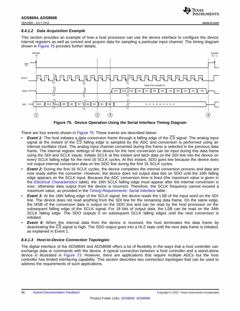
1 2 14 15 16 17 25 26 27 28 29 30 31 32SCLK
CS
D9 D8 D7 D6 D5 D4SDO
Sample N
Sample N + 1
Data from sample N
33 34
D17 D16
18
D3 D2 D1 D0
B15 B14 B2 B1 B0 X X X X X X X X XSDI
7 8 9
B9 B8 B7B10 B3
1 2 3 4
ADS8694, ADS8698SBAS686 –JULY 2015 www.ti.com
8.4.1.2 Data Acquisition ExampleThis section provides an example of how a host processor can use the device interface to configure the deviceinternal registers as well as convert and acquire data for sampling a particular input channel. The timing diagramshown in Figure 75 provides further details.
Figure 75. Device Operation Using the Serial Interface Timing Diagram
There are four events shown in Figure 75. These events are described below:• Event 1: The host initiates a data conversion frame through a falling edge of the CS signal. The analog input
signal at the instant of the CS falling edge is sampled by the ADC and conversion is performed using aninternal oscillator clock. The analog input channel converted during this frame is selected in the previous dataframe. The internal register settings of the device for the next conversion can be input during this data frameusing the SDI and SCLK inputs. Initiate SCLK at this instant and latch data on the SDI line into the device onevery SCLK falling edge for the next 16 SCLK cycles. At this instant, SDO goes low because the device doesnot output internal conversion data on the SDO line during the first 16 SCLK cycles.
• Event 2: During the first 16 SCLK cycles, the device completes the internal conversion process and data arenow ready within the converter. However, the device does not output data bits on SDO until the 16th fallingedge appears on the SCLK input. Because the ADC conversion time is fixed (the maximum value is given inthe Electrical Characteristics table), the 16th SCLK falling edge must appear after the internal conversion isover, otherwise data output from the device is incorrect. Therefore, the SCLK frequency cannot exceed amaximum value, as provided in the Timing Requirements: Serial Interface table.
• Event 3: At the 16th falling edge of the SCLK signal, the device reads the LSB of the input word on the SDIline. The device does not read anything from the SDI line for the remaining data frame. On the same edge,the MSB of the conversion data is output on the SDO line and can be read by the host processor on thesubsequent falling edge of the SCLK signal. For 18 bits of output data, the LSB can be read on the 34thSCLK falling edge. The SDO outputs 0 on subsequent SCLK falling edges until the next conversion isinitiated.
• Event 4: When the internal data from the device is received, the host terminates the data frame bydeactivating the CS signal to high. The SDO output goes into a Hi-Z state until the next data frame is initiated,as explained in Event 1.
8.4.1.3 Host-to-Device Connection TopologiesThe digital interface of the ADS8694 and ADS8698 offers a lot of flexibility in the ways that a host controller canexchange data or commands with the device. A typical connection between a host controller and a stand-alonedevice is illustrated in Figure 73. However, there are applications that require multiple ADCs but the hostcontroller has limited interfacing capability. This section describes two connection topologies that can be used toaddress the requirements of such applications.
36 Submit Documentation Feedback Copyright © 2015, Texas Instruments Incorporated
Product Folder Links: ADS8694 ADS8698
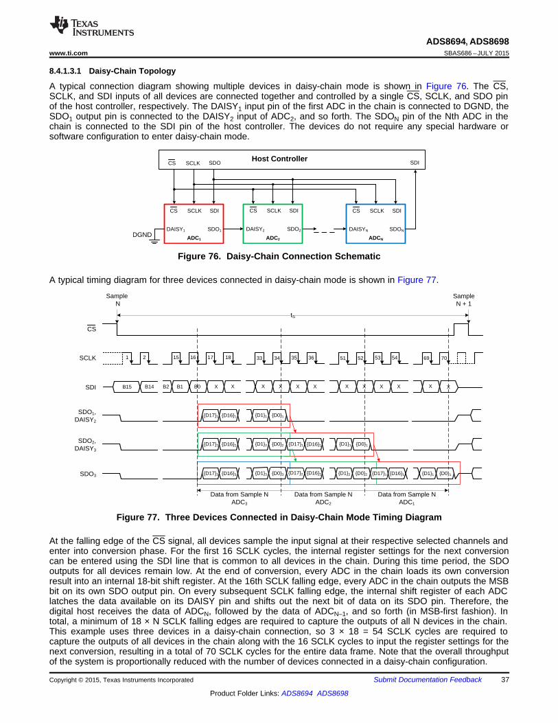
1 2 15 16 17SCLK
CS
Sample N
Sample N + 1
tS
33 3418
B15 B14 X X X XSDI XB1 B0 XB2
35 36 51 52 53 54 69 70
X X X X X X
SDO3
Data from Sample NADC3
SDO2, DAISY3
SDO1, DAISY2
{D17}1 {D16}1 {D1}1 {D0}1
{D17}2 {D16}2 {D1}2 {D0}2
{D17}3 {D16}3 {D1}3 {D0}3
{D17}1 {D16}1 {D1}1 {D0}1
{D17}2 {D16}2 {D1}2 {D0}2 {D17}1 {D16}1 {D1}1 {D0}1
Data from Sample NADC2
Data from Sample NADC1
CS SDISCLK
DAISY1 SDO1
SDI
DGND ADC1 ADC2 ADCN
CS SDOSCLKHost Controller
CS SDISCLK
DAISY2 SDO2
CS SDISCLK
DAISYN SDON
ADS8694, ADS8698www.ti.com SBAS686 –JULY 2015
8.4.1.3.1 Daisy-Chain Topology
A typical connection diagram showing multiple devices in daisy-chain mode is shown in Figure 76. The CS,SCLK, and SDI inputs of all devices are connected together and controlled by a single CS, SCLK, and SDO pinof the host controller, respectively. The DAISY1 input pin of the first ADC in the chain is connected to DGND, theSDO1 output pin is connected to the DAISY2 input of ADC2, and so forth. The SDON pin of the Nth ADC in thechain is connected to the SDI pin of the host controller. The devices do not require any special hardware orsoftware configuration to enter daisy-chain mode.
Figure 76. Daisy-Chain Connection Schematic
A typical timing diagram for three devices connected in daisy-chain mode is shown in Figure 77.
Figure 77. Three Devices Connected in Daisy-Chain Mode Timing Diagram
At the falling edge of the CS signal, all devices sample the input signal at their respective selected channels andenter into conversion phase. For the first 16 SCLK cycles, the internal register settings for the next conversioncan be entered using the SDI line that is common to all devices in the chain. During this time period, the SDOoutputs for all devices remain low. At the end of conversion, every ADC in the chain loads its own conversionresult into an internal 18-bit shift register. At the 16th SCLK falling edge, every ADC in the chain outputs the MSBbit on its own SDO output pin. On every subsequent SCLK falling edge, the internal shift register of each ADClatches the data available on its DAISY pin and shifts out the next bit of data on its SDO pin. Therefore, thedigital host receives the data of ADCN, followed by the data of ADCN–1, and so forth (in MSB-first fashion). Intotal, a minimum of 18 × N SCLK falling edges are required to capture the outputs of all N devices in the chain.This example uses three devices in a daisy-chain connection, so 3 × 18 = 54 SCLK cycles are required tocapture the outputs of all devices in the chain along with the 16 SCLK cycles to input the register settings for thenext conversion, resulting in a total of 70 SCLK cycles for the entire data frame. Note that the overall throughputof the system is proportionally reduced with the number of devices connected in a daisy-chain configuration.
Copyright © 2015, Texas Instruments Incorporated Submit Documentation Feedback 37
Product Folder Links: ADS8694 ADS8698
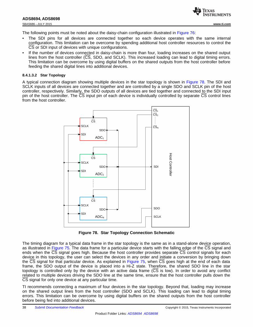
CS
SDOSCLK
SDI
CS
SDOSCLK
SDI
CS
SDOSCLK
SDI
SDO
SCLK
ADC1
ADC2
ADCN
SDI
CS1
CS2
CSN
Host C
ontroller
ADS8694, ADS8698SBAS686 –JULY 2015 www.ti.com
The following points must be noted about the daisy-chain configuration illustrated in Figure 76:• The SDI pins for all devices are connected together so each device operates with the same internal
configuration. This limitation can be overcome by spending additional host controller resources to control theCS or SDI input of devices with unique configurations.
• If the number of devices connected in daisy-chain is more than four, loading increases on the shared outputlines from the host controller (CS, SDO, and SCLK). This increased loading can lead to digital timing errors.This limitation can be overcome by using digital buffers on the shared outputs from the host controller beforefeeding the shared digital lines into additional devices.
8.4.1.3.2 Star Topology
A typical connection diagram showing multiple devices in the star topology is shown in Figure 78. The SDI andSCLK inputs of all devices are connected together and are controlled by a single SDO and SCLK pin of the hostcontroller, respectively. Similarly, the SDO outputs of all devices are tied together and connected to the SDI inputpin of the host controller. The CS input pin of each device is individually controlled by separate CS control linesfrom the host controller.
Figure 78. Star Topology Connection Schematic
The timing diagram for a typical data frame in the star topology is the same as in a stand-alone device operation,as illustrated in Figure 75. The data frame for a particular device starts with the falling edge of the CS signal andends when the CS signal goes high. Because the host controller provides separate CS control signals for eachdevice in this topology, the user can select the devices in any order and initiate a conversion by bringing downthe CS signal for that particular device. As explained in Figure 75, when CS goes high at the end of each dataframe, the SDO output of the device is placed into a Hi-Z state. Therefore, the shared SDO line in the startopology is controlled only by the device with an active data frame (CS is low). In order to avoid any conflictrelated to multiple devices driving the SDO line at the same time, ensure that the host controller pulls down theCS signal for only one device at any particular time.
TI recommends connecting a maximum of four devices in the star topology. Beyond that, loading may increaseon the shared output lines from the host controller (SDO and SCLK). This loading can lead to digital timingerrors. This limitation can be overcome by using digital buffers on the shared outputs from the host controllerbefore being fed into additional devices.38 Submit Documentation Feedback Copyright © 2015, Texas Instruments Incorporated
Product Folder Links: ADS8694 ADS8698
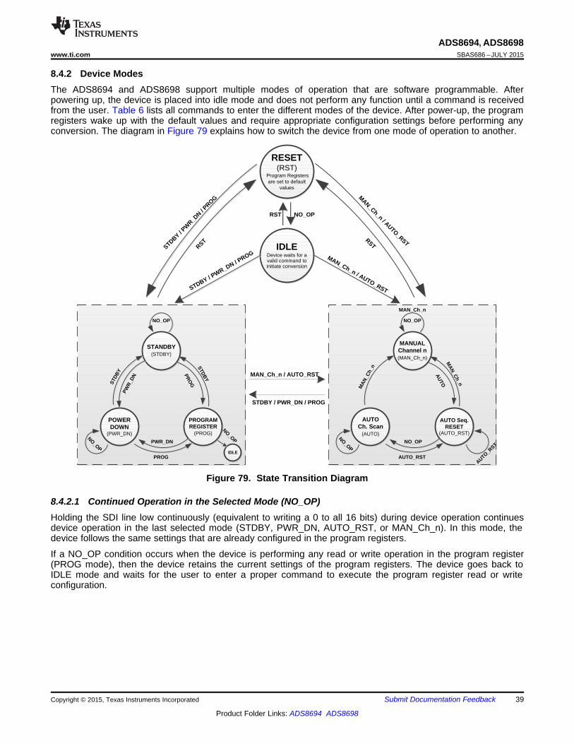
STANDBY(STDBY)
POWERDOWN
(PWR_DN)
PROGRAMREGISTER
(PROG)
STD
BY
PWR
_DN
STDB
Y
PRO
G
PWR_DN
PROG
NO_OPNO_OP
NO_OP
MANUALChannel n(MAN_Ch_n)
AUTO Ch. Scan
(AUTO)
AUTO Seq.RESET
(AUTO_RST)
MA
N_C
h_n
MA
N_C
h_n
AU
TO
NO_OP
AUTO_RSTAUTO_R
ST
NO_OP
NO_OP
MAN_Ch_n
IDLEDevice waits for a valid command to initiate conversion
RESET(RST)
Program Registers are set to default
values
STDBY / PWR_DN / P
ROG MAN_Ch_n / AUTO_RST
NO_OPRST
MAN_Ch_n / AUTO_RST
STDBY / PWR_DN / PROG
STDBY / PW
R_DN / P
ROG
RST
MAN_Ch_n / AUTO_RSTRST
IDLE
ADS8694, ADS8698www.ti.com SBAS686 –JULY 2015
8.4.2 Device ModesThe ADS8694 and ADS8698 support multiple modes of operation that are software programmable. Afterpowering up, the device is placed into idle mode and does not perform any function until a command is receivedfrom the user. Table 6 lists all commands to enter the different modes of the device. After power-up, the programregisters wake up with the default values and require appropriate configuration settings before performing anyconversion. The diagram in Figure 79 explains how to switch the device from one mode of operation to another.
Figure 79. State Transition Diagram
8.4.2.1 Continued Operation in the Selected Mode (NO_OP)Holding the SDI line low continuously (equivalent to writing a 0 to all 16 bits) during device operation continuesdevice operation in the last selected mode (STDBY, PWR_DN, AUTO_RST, or MAN_Ch_n). In this mode, thedevice follows the same settings that are already configured in the program registers.
If a NO_OP condition occurs when the device is performing any read or write operation in the program register(PROG mode), then the device retains the current settings of the program registers. The device goes back toIDLE mode and waits for the user to enter a proper command to execute the program register read or writeconfiguration.
Copyright © 2015, Texas Instruments Incorporated Submit Documentation Feedback 39
Product Folder Links: ADS8694 ADS8698
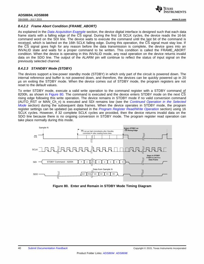
1 2 14 15 16 17 18 32 33 34SCLK
CS
D3SDO
Data from Sample N
D17 D16 D2 D1 D0
STDBY Command ± 8200hSDI X X X X X X X X
Sample N Enters STDBY on CS Rising EdgeCS can go high immediately after Standby
command or after reading frame data.
1 2 14 15 16
Stays in STDBY if SDI is Low in a
Data Frame
ADS8694, ADS8698SBAS686 –JULY 2015 www.ti.com
8.4.2.2 Frame Abort Condition (FRAME_ABORT)As explained in the Data Acquisition Example section, the device digital interface is designed such that each dataframe starts with a falling edge of the CS signal. During the first 16 SCLK cycles, the device reads the 16-bitcommand word on the SDI line. The device waits to execute the command until the last bit of the command isreceived, which is latched on the 16th SCLK falling edge. During this operation, the CS signal must stay low. Ifthe CS signal goes high for any reason before the data transmission is complete, the device goes into anINVALID state and waits for a proper command to be written. This condition is called the FRAME_ABORTcondition. When the device is operating in this INVALID mode, any read operation on the device returns invaliddata on the SDO line. The output of the ALARM pin will continue to reflect the status of input signal on thepreviously selected channel.
8.4.2.3 STANDBY Mode (STDBY)The devices support a low-power standby mode (STDBY) in which only part of the circuit is powered down. Theinternal reference and buffer is not powered down, and therefore, the devices can be quickly powered up in 20µs on exiting the STDBY mode. When the device comes out of STDBY mode, the program registers are notreset to the default values.
To enter STDBY mode, execute a valid write operation to the command register with a STDBY command of8200h, as shown in Figure 80. The command is executed and the device enters STDBY mode on the next CSrising edge following this write operation. The device remains in STDBY mode if no valid conversion command(AUTO_RST or MAN_Ch_n) is executed and SDI remains low (see the Continued Operation in the SelectedMode section) during the subsequent data frames. When the device operates in STDBY mode, the programregister settings can be updated (as explained in the Program Register Read/Write Operation section) using 16SCLK cycles. However, if 32 complete SCLK cycles are provided, then the device returns invalid data on theSDO line because there is no ongoing conversion in STDBY mode. The program register read operation cantake place normally during this mode.
Figure 80. Enter and Remain in STDBY Mode Timing Diagram
40 Submit Documentation Feedback Copyright © 2015, Texas Instruments Incorporated
Product Folder Links: ADS8694 ADS8698
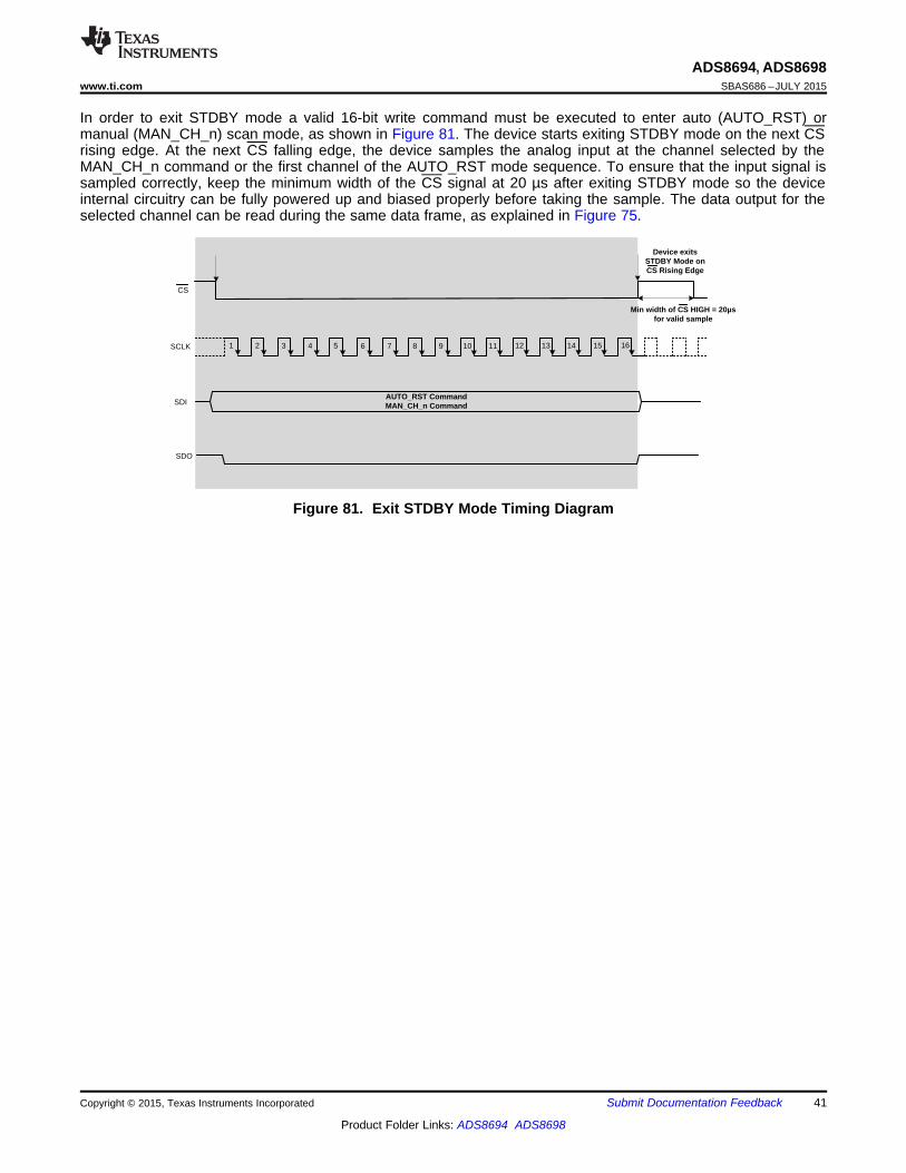
1 2 12 13 14 15 16SCLK
CS
SDO
AUTO_RST CommandMAN_CH_n CommandSDI
9 10 113 4 5 6 7 8
Device exits STDBY Mode on CS Rising Edge
Min width of CS HIGH = 20µs for valid sample
ADS8694, ADS8698www.ti.com SBAS686 –JULY 2015
In order to exit STDBY mode a valid 16-bit write command must be executed to enter auto (AUTO_RST) ormanual (MAN_CH_n) scan mode, as shown in Figure 81. The device starts exiting STDBY mode on the next CSrising edge. At the next CS falling edge, the device samples the analog input at the channel selected by theMAN_CH_n command or the first channel of the AUTO_RST mode sequence. To ensure that the input signal issampled correctly, keep the minimum width of the CS signal at 20 µs after exiting STDBY mode so the deviceinternal circuitry can be fully powered up and biased properly before taking the sample. The data output for theselected channel can be read during the same data frame, as explained in Figure 75.
Figure 81. Exit STDBY Mode Timing Diagram
Copyright © 2015, Texas Instruments Incorporated Submit Documentation Feedback 41
Product Folder Links: ADS8694 ADS8698
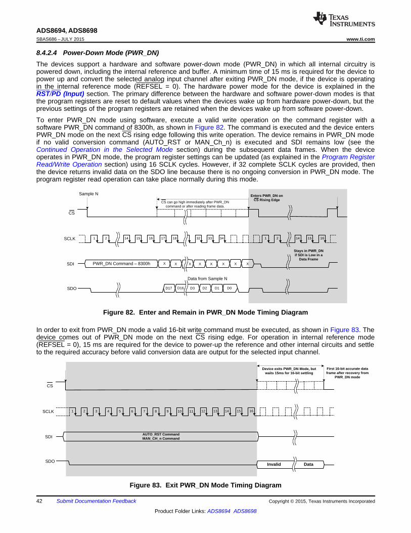
1 2 12 13 14 15 16SCLK
CS
SDO
AUTO_RST CommandMAN_CH_n CommandSDI
9 10 113 4 5 6 7 8
Device exits PWR_DN Mode, but waits 15ms for 16-bit settling
First 16-bit accurate data frame after recovery from
PWR_DN mode
Invalid Data
1 2 14 15 16 17 18 32 33 34SCLK
CS
D3SDO
Data from Sample N
D17 D16 D2 D1 D0
PWR_DN Command ± 8300hSDI X X X X X X X X
Sample N Enters PWR_DN on CS Rising Edge
CS can go high immediately after PWR_DN command or after reading frame data.
1 2 14 15 16
Stays in PWR_DN if SDI is Low in a
Data Frame
ADS8694, ADS8698SBAS686 –JULY 2015 www.ti.com
8.4.2.4 Power-Down Mode (PWR_DN)The devices support a hardware and software power-down mode (PWR_DN) in which all internal circuitry ispowered down, including the internal reference and buffer. A minimum time of 15 ms is required for the device topower up and convert the selected analog input channel after exiting PWR_DN mode, if the device is operatingin the internal reference mode (REFSEL = 0). The hardware power mode for the device is explained in theRST/PD (Input) section. The primary difference between the hardware and software power-down modes is thatthe program registers are reset to default values when the devices wake up from hardware power-down, but theprevious settings of the program registers are retained when the devices wake up from software power-down.
To enter PWR_DN mode using software, execute a valid write operation on the command register with asoftware PWR_DN command of 8300h, as shown in Figure 82. The command is executed and the device entersPWR_DN mode on the next CS rising edge following this write operation. The device remains in PWR_DN modeif no valid conversion command (AUTO_RST or MAN_Ch_n) is executed and SDI remains low (see theContinued Operation in the Selected Mode section) during the subsequent data frames. When the deviceoperates in PWR_DN mode, the program register settings can be updated (as explained in the Program RegisterRead/Write Operation section) using 16 SCLK cycles. However, if 32 complete SCLK cycles are provided, thenthe device returns invalid data on the SDO line because there is no ongoing conversion in PWR_DN mode. Theprogram register read operation can take place normally during this mode.
Figure 82. Enter and Remain in PWR_DN Mode Timing Diagram
In order to exit from PWR_DN mode a valid 16-bit write command must be executed, as shown in Figure 83. Thedevice comes out of PWR_DN mode on the next CS rising edge. For operation in internal reference mode(REFSEL = 0), 15 ms are required for the device to power-up the reference and other internal circuits and settleto the required accuracy before valid conversion data are output for the selected input channel.
Figure 83. Exit PWR_DN Mode Timing Diagram
42 Submit Documentation Feedback Copyright © 2015, Texas Instruments Incorporated
Product Folder Links: ADS8694 ADS8698
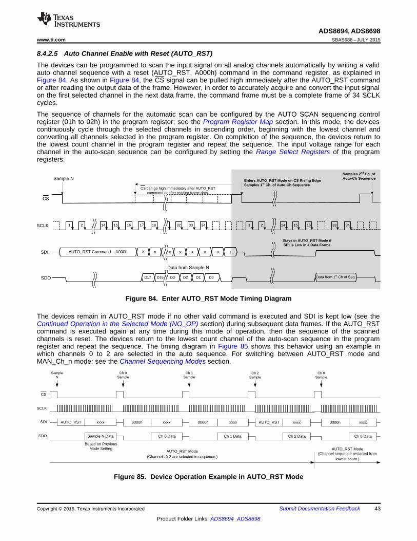
AUTO_RST
SampleN
SCLK
SDI
SDO
CS
xxxx
Sample N Data
Ch 0 Sample
0000h xxxx
Ch 0 Data
Ch 1 Sample
0000h xxxx
Ch 1 Data
Ch 2 Sample
AUTO_RST xxxx
Ch 2 Data
Based on Previous Mode Setting
Ch 0 Sample
0000h xxxx
Ch 0 Data
AUTO_RST Mode(Channel sequence restarted from
lowest count.)
AUTO_RST Mode(Channels 0-2 are selected in sequence.)
1 2 14 15 16 17 18 32 33 34SCLK
CS
D3SDO
Data from Sample N
D17 D16 D2 D1 D0
AUTO_RST Command ± A000hSDI X X X X X X X X
Sample N Enters AUTO_RST Mode on CS Rising EdgeSamples 1st Ch. of Auto-Ch Sequence
CS can go high immediately after AUTO_RST command or after reading frame data.
1 2 14 15 16
Stays in AUTO_RST Mode if SDI is Low in a Data Frame
33 34
Samples 2nd Ch. of Auto-Ch Sequence
Data from 1st Ch of Seq.
ADS8694, ADS8698www.ti.com SBAS686 –JULY 2015
8.4.2.5 Auto Channel Enable with Reset (AUTO_RST)The devices can be programmed to scan the input signal on all analog channels automatically by writing a validauto channel sequence with a reset (AUTO_RST, A000h) command in the command register, as explained inFigure 84. As shown in Figure 84, the CS signal can be pulled high immediately after the AUTO_RST commandor after reading the output data of the frame. However, in order to accurately acquire and convert the input signalon the first selected channel in the next data frame, the command frame must be a complete frame of 34 SCLKcycles.
The sequence of channels for the automatic scan can be configured by the AUTO SCAN sequencing controlregister (01h to 02h) in the program register; see the Program Register Map section. In this mode, the devicescontinuously cycle through the selected channels in ascending order, beginning with the lowest channel andconverting all channels selected in the program register. On completion of the sequence, the devices return tothe lowest count channel in the program register and repeat the sequence. The input voltage range for eachchannel in the auto-scan sequence can be configured by setting the Range Select Registers of the programregisters.
Figure 84. Enter AUTO_RST Mode Timing Diagram
The devices remain in AUTO_RST mode if no other valid command is executed and SDI is kept low (see theContinued Operation in the Selected Mode (NO_OP) section) during subsequent data frames. If the AUTO_RSTcommand is executed again at any time during this mode of operation, then the sequence of the scannedchannels is reset. The devices return to the lowest count channel of the auto-scan sequence in the programregister and repeat the sequence. The timing diagram in Figure 85 shows this behavior using an example inwhich channels 0 to 2 are selected in the auto sequence. For switching between AUTO_RST mode andMAN_Ch_n mode; see the Channel Sequencing Modes section.
Figure 85. Device Operation Example in AUTO_RST Mode
Copyright © 2015, Texas Instruments Incorporated Submit Documentation Feedback 43
Product Folder Links: ADS8694 ADS8698
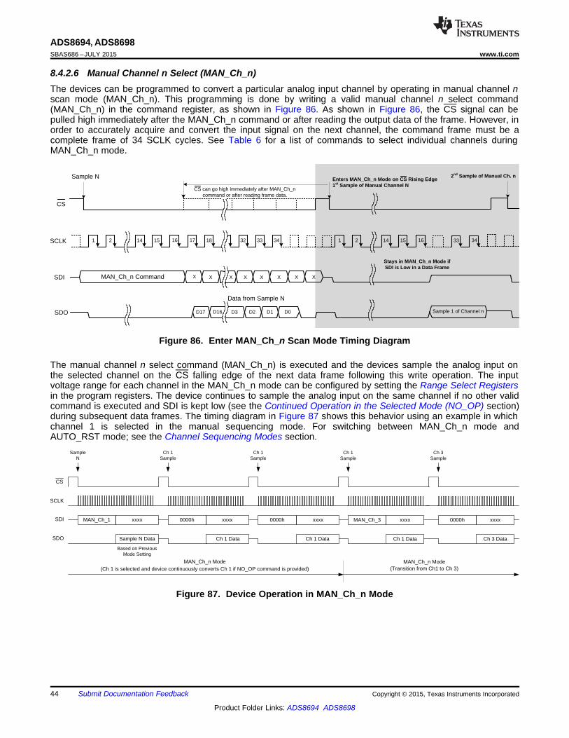
MAN_Ch_1
SampleN
SCLK
SDI
SDO
CS
xxxx
Sample N Data
Ch 1 Sample
0000h xxxx
Ch 1 Data
Ch 1 Sample
0000h xxxx
Ch 1 Data
Ch 1 Sample
MAN_Ch_3 xxxx
Ch 1 Data
Based on Previous Mode Setting
Ch 3 Sample
0000h xxxx
Ch 3 Data
MAN_Ch_n Mode(Ch 1 is selected and device continuously converts Ch 1 if NO_OP command is provided)
MAN_Ch_n Mode(Transition from Ch1 to Ch 3)
1 2 14 15 16 17 18 32 33 34SCLK
CS
D3SDO
Data from Sample N
D17 D16 D2 D1 D0
MAN_Ch_n CommandSDI X X X X X X X X
Sample N Enters MAN_Ch_n Mode on CS Rising Edge1st Sample of Manual Channel N
CS can go high immediately after MAN_Ch_n command or after reading frame data.
1 2 14 15 16
Stays in MAN_Ch_n Mode if SDI is Low in a Data Frame
33 34
2nd Sample of Manual Ch. n
Sample 1 of Channel n
ADS8694, ADS8698SBAS686 –JULY 2015 www.ti.com
8.4.2.6 Manual Channel n Select (MAN_Ch_n)The devices can be programmed to convert a particular analog input channel by operating in manual channel nscan mode (MAN_Ch_n). This programming is done by writing a valid manual channel n select command(MAN_Ch_n) in the command register, as shown in Figure 86. As shown in Figure 86, the CS signal can bepulled high immediately after the MAN_Ch_n command or after reading the output data of the frame. However, inorder to accurately acquire and convert the input signal on the next channel, the command frame must be acomplete frame of 34 SCLK cycles. See Table 6 for a list of commands to select individual channels duringMAN_Ch_n mode.
Figure 86. Enter MAN_Ch_n Scan Mode Timing Diagram
The manual channel n select command (MAN_Ch_n) is executed and the devices sample the analog input onthe selected channel on the CS falling edge of the next data frame following this write operation. The inputvoltage range for each channel in the MAN_Ch_n mode can be configured by setting the Range Select Registersin the program registers. The device continues to sample the analog input on the same channel if no other validcommand is executed and SDI is kept low (see the Continued Operation in the Selected Mode (NO_OP) section)during subsequent data frames. The timing diagram in Figure 87 shows this behavior using an example in whichchannel 1 is selected in the manual sequencing mode. For switching between MAN_Ch_n mode andAUTO_RST mode; see the Channel Sequencing Modes section.
Figure 87. Device Operation in MAN_Ch_n Mode
44 Submit Documentation Feedback Copyright © 2015, Texas Instruments Incorporated
Product Folder Links: ADS8694 ADS8698
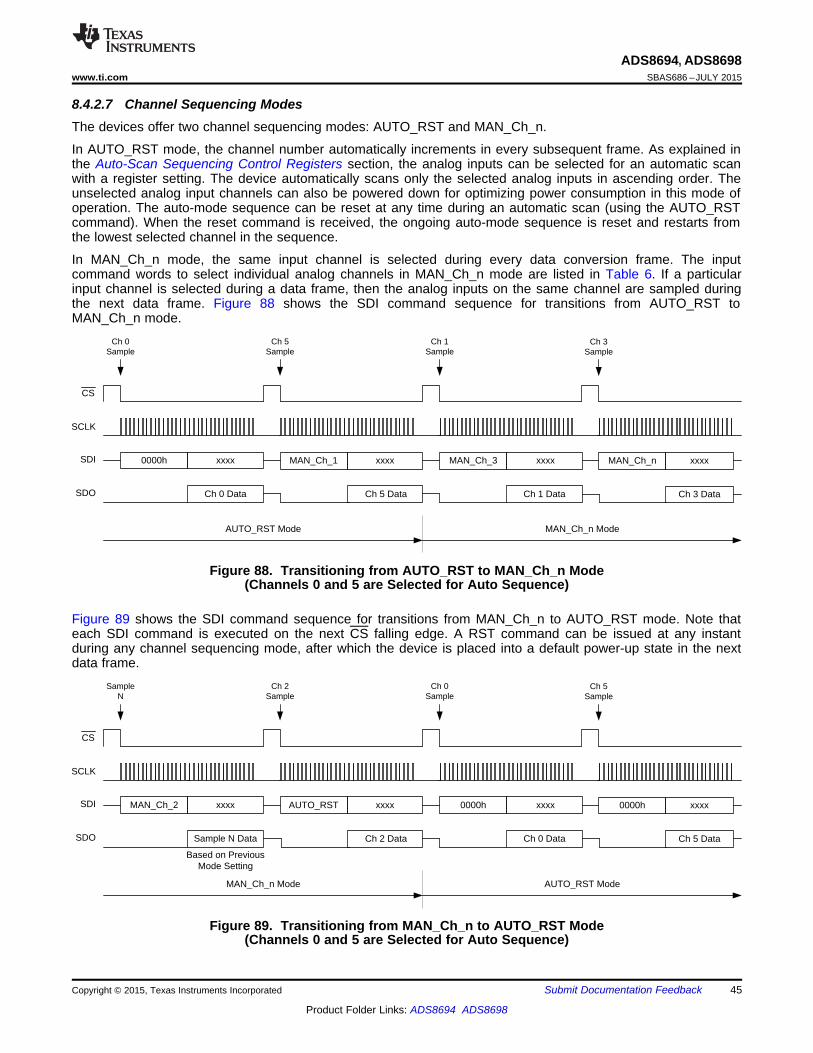
MAN_Ch_2
SCLK
SDI
SDO
AUTO_RST ModeMAN_Ch_n Mode
CS
xxxx
Ch 2 Sample
AUTO_RST xxxx
Ch 2 Data
Ch 0 Sample
0000h xxxx
Ch 0 Data
Ch 5 Sample
0000h xxxx
Ch 5 Data
SampleN
Sample N Data
Based on Previous Mode Setting
0000h
Ch 0 Sample
SCLK
SDI
SDO
MAN_Ch_n ModeAUTO_RST Mode
CS
xxxx
Ch 0 Data
Ch 5 Sample
MAN_Ch_1 xxxx
Ch 5 Data
Ch 1 Sample
MAN_Ch_3 xxxx
Ch 1 Data
Ch 3 Sample
MAN_Ch_n xxxx
Ch 3 Data
ADS8694, ADS8698www.ti.com SBAS686 –JULY 2015
8.4.2.7 Channel Sequencing ModesThe devices offer two channel sequencing modes: AUTO_RST and MAN_Ch_n.
In AUTO_RST mode, the channel number automatically increments in every subsequent frame. As explained inthe Auto-Scan Sequencing Control Registers section, the analog inputs can be selected for an automatic scanwith a register setting. The device automatically scans only the selected analog inputs in ascending order. Theunselected analog input channels can also be powered down for optimizing power consumption in this mode ofoperation. The auto-mode sequence can be reset at any time during an automatic scan (using the AUTO_RSTcommand). When the reset command is received, the ongoing auto-mode sequence is reset and restarts fromthe lowest selected channel in the sequence.
In MAN_Ch_n mode, the same input channel is selected during every data conversion frame. The inputcommand words to select individual analog channels in MAN_Ch_n mode are listed in Table 6. If a particularinput channel is selected during a data frame, then the analog inputs on the same channel are sampled duringthe next data frame. Figure 88 shows the SDI command sequence for transitions from AUTO_RST toMAN_Ch_n mode.
Figure 88. Transitioning from AUTO_RST to MAN_Ch_n Mode(Channels 0 and 5 are Selected for Auto Sequence)
Figure 89 shows the SDI command sequence for transitions from MAN_Ch_n to AUTO_RST mode. Note thateach SDI command is executed on the next CS falling edge. A RST command can be issued at any instantduring any channel sequencing mode, after which the device is placed into a default power-up state in the nextdata frame.
Figure 89. Transitioning from MAN_Ch_n to AUTO_RST Mode(Channels 0 and 5 are Selected for Auto Sequence)
Copyright © 2015, Texas Instruments Incorporated Submit Documentation Feedback 45
Product Folder Links: ADS8694 ADS8698
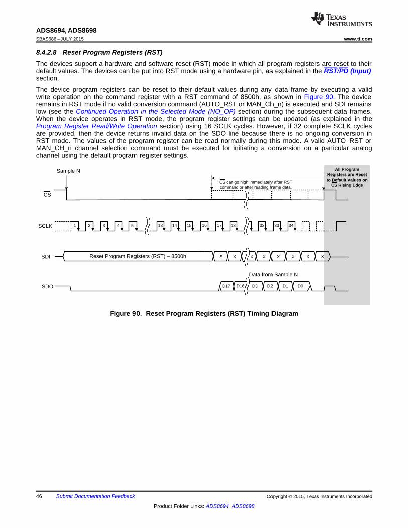
1 2 13 14 15 16 17 18 32 33 34SCLK
CS
D3SDO
Data from Sample N
D17 D16 D2 D1 D0
Reset Program Registers (RST) ± 8500hSDI X X X X X X
3 4 5
X X
Sample N All Program Registers are Reset to Default Values on
CS Rising EdgeCS can go high immediately after RST command or after reading frame data.
ADS8694, ADS8698SBAS686 –JULY 2015 www.ti.com
8.4.2.8 Reset Program Registers (RST)The devices support a hardware and software reset (RST) mode in which all program registers are reset to theirdefault values. The devices can be put into RST mode using a hardware pin, as explained in the RST/PD (Input)section.
The device program registers can be reset to their default values during any data frame by executing a validwrite operation on the command register with a RST command of 8500h, as shown in Figure 90. The deviceremains in RST mode if no valid conversion command (AUTO_RST or MAN_Ch_n) is executed and SDI remainslow (see the Continued Operation in the Selected Mode (NO_OP) section) during the subsequent data frames.When the device operates in RST mode, the program register settings can be updated (as explained in theProgram Register Read/Write Operation section) using 16 SCLK cycles. However, if 32 complete SCLK cyclesare provided, then the device returns invalid data on the SDO line because there is no ongoing conversion inRST mode. The values of the program register can be read normally during this mode. A valid AUTO_RST orMAN_CH_n channel selection command must be executed for initiating a conversion on a particular analogchannel using the default program register settings.
Figure 90. Reset Program Registers (RST) Timing Diagram
46 Submit Documentation Feedback Copyright © 2015, Texas Instruments Incorporated
Product Folder Links: ADS8694 ADS8698
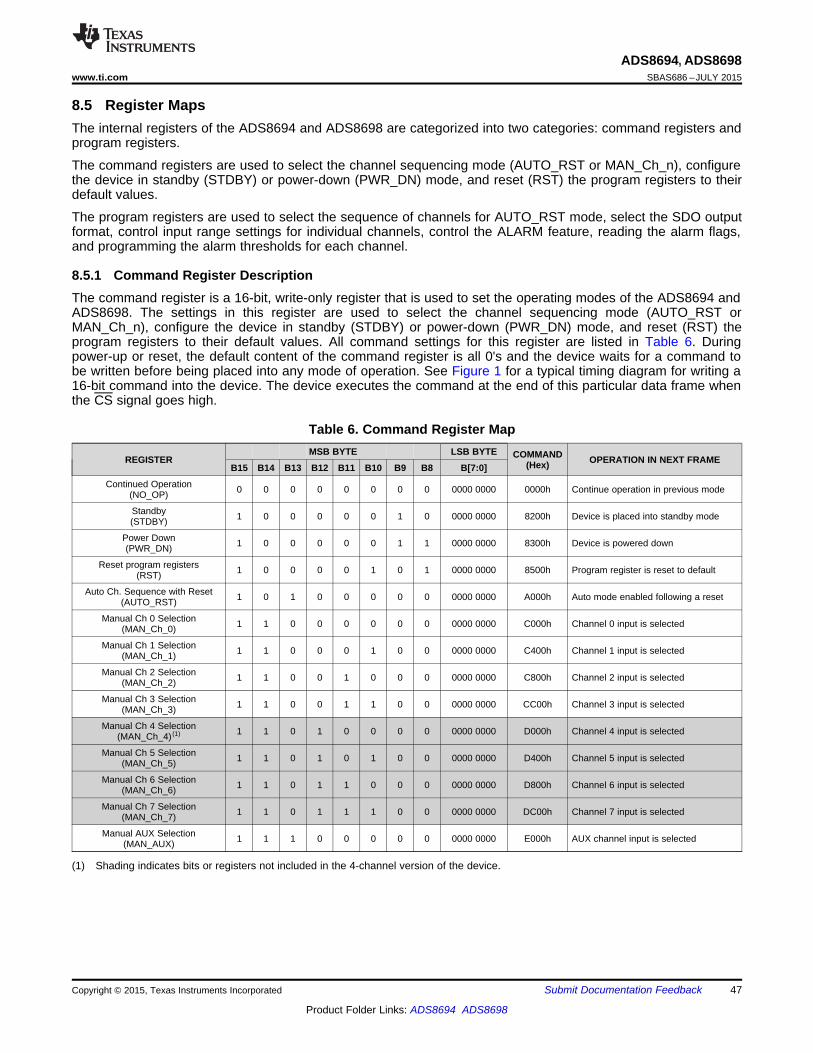
ADS8694, ADS8698www.ti.com SBAS686 –JULY 2015
8.5 Register MapsThe internal registers of the ADS8694 and ADS8698 are categorized into two categories: command registers andprogram registers.
The command registers are used to select the channel sequencing mode (AUTO_RST or MAN_Ch_n), configurethe device in standby (STDBY) or power-down (PWR_DN) mode, and reset (RST) the program registers to theirdefault values.
The program registers are used to select the sequence of channels for AUTO_RST mode, select the SDO outputformat, control input range settings for individual channels, control the ALARM feature, reading the alarm flags,and programming the alarm thresholds for each channel.
8.5.1 Command Register DescriptionThe command register is a 16-bit, write-only register that is used to set the operating modes of the ADS8694 andADS8698. The settings in this register are used to select the channel sequencing mode (AUTO_RST orMAN_Ch_n), configure the device in standby (STDBY) or power-down (PWR_DN) mode, and reset (RST) theprogram registers to their default values. All command settings for this register are listed in Table 6. Duringpower-up or reset, the default content of the command register is all 0's and the device waits for a command tobe written before being placed into any mode of operation. See Figure 1 for a typical timing diagram for writing a16-bit command into the device. The device executes the command at the end of this particular data frame whenthe CS signal goes high.
Table 6. Command Register MapMSB BYTE LSB BYTE COMMANDREGISTER OPERATION IN NEXT FRAME(Hex)B15 B14 B13 B12 B11 B10 B9 B8 B[7:0]
Continued Operation 0 0 0 0 0 0 0 0 0000 0000 0000h Continue operation in previous mode(NO_OP)
Standby 1 0 0 0 0 0 1 0 0000 0000 8200h Device is placed into standby mode(STDBY)
Power Down 1 0 0 0 0 0 1 1 0000 0000 8300h Device is powered down(PWR_DN)
Reset program registers 1 0 0 0 0 1 0 1 0000 0000 8500h Program register is reset to default(RST)
Auto Ch. Sequence with Reset 1 0 1 0 0 0 0 0 0000 0000 A000h Auto mode enabled following a reset(AUTO_RST)
Manual Ch 0 Selection 1 1 0 0 0 0 0 0 0000 0000 C000h Channel 0 input is selected(MAN_Ch_0)
Manual Ch 1 Selection 1 1 0 0 0 1 0 0 0000 0000 C400h Channel 1 input is selected(MAN_Ch_1)
Manual Ch 2 Selection 1 1 0 0 1 0 0 0 0000 0000 C800h Channel 2 input is selected(MAN_Ch_2)
Manual Ch 3 Selection 1 1 0 0 1 1 0 0 0000 0000 CC00h Channel 3 input is selected(MAN_Ch_3)
Manual Ch 4 Selection 1 1 0 1 0 0 0 0 0000 0000 D000h Channel 4 input is selected(MAN_Ch_4) (1)
Manual Ch 5 Selection 1 1 0 1 0 1 0 0 0000 0000 D400h Channel 5 input is selected(MAN_Ch_5)
Manual Ch 6 Selection 1 1 0 1 1 0 0 0 0000 0000 D800h Channel 6 input is selected(MAN_Ch_6)
Manual Ch 7 Selection 1 1 0 1 1 1 0 0 0000 0000 DC00h Channel 7 input is selected(MAN_Ch_7)
Manual AUX Selection 1 1 1 0 0 0 0 0 0000 0000 E000h AUX channel input is selected(MAN_AUX)
(1) Shading indicates bits or registers not included in the 4-channel version of the device.
Copyright © 2015, Texas Instruments Incorporated Submit Documentation Feedback 47
Product Folder Links: ADS8694 ADS8698
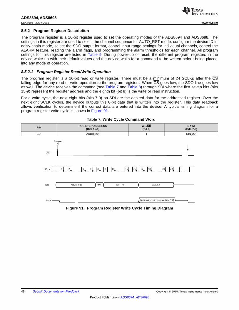
1 2 15 16SCLK
CS
SDO
ADDR [6:0] WR DIN [7:0]SDI
9 106 7 8
Data written into register, DIN [7:0]
23 2417 18
X X X X
Sample N
ADS8694, ADS8698SBAS686 –JULY 2015 www.ti.com
8.5.2 Program Register DescriptionThe program register is a 16-bit register used to set the operating modes of the ADS8694 and ADS8698. Thesettings in this register are used to select the channel sequence for AUTO_RST mode, configure the device ID indaisy-chain mode, select the SDO output format, control input range settings for individual channels, control theALARM feature, reading the alarm flags, and programming the alarm thresholds for each channel. All programsettings for this register are listed in Table 9. During power-up or reset, the different program registers in thedevice wake up with their default values and the device waits for a command to be written before being placedinto any mode of operation.
8.5.2.1 Program Register Read/Write OperationThe program register is a 16-bit read or write register. There must be a minimum of 24 SCLKs after the CSfalling edge for any read or write operation to the program registers. When CS goes low, the SDO line goes lowas well. The device receives the command (see Table 7 and Table 8) through SDI where the first seven bits (bits15-9) represent the register address and the eighth bit (bit 8) is the write or read instruction.
For a write cycle, the next eight bits (bits 7-0) on SDI are the desired data for the addressed register. Over thenext eight SCLK cycles, the device outputs this 8-bit data that is written into the register. This data readbackallows verification to determine if the correct data are entered into the device. A typical timing diagram for aprogram register write cycle is shown in Figure 91.
Table 7. Write Cycle Command WordREGISTER ADDRESS WR/RD DATAPIN (Bits 15-9) (Bit 8) (Bits 7-0)
SDI ADDR[6:0] 1 DIN[7:0]
Figure 91. Program Register Write Cycle Timing Diagram
48 Submit Documentation Feedback Copyright © 2015, Texas Instruments Incorporated
Product Folder Links: ADS8694 ADS8698
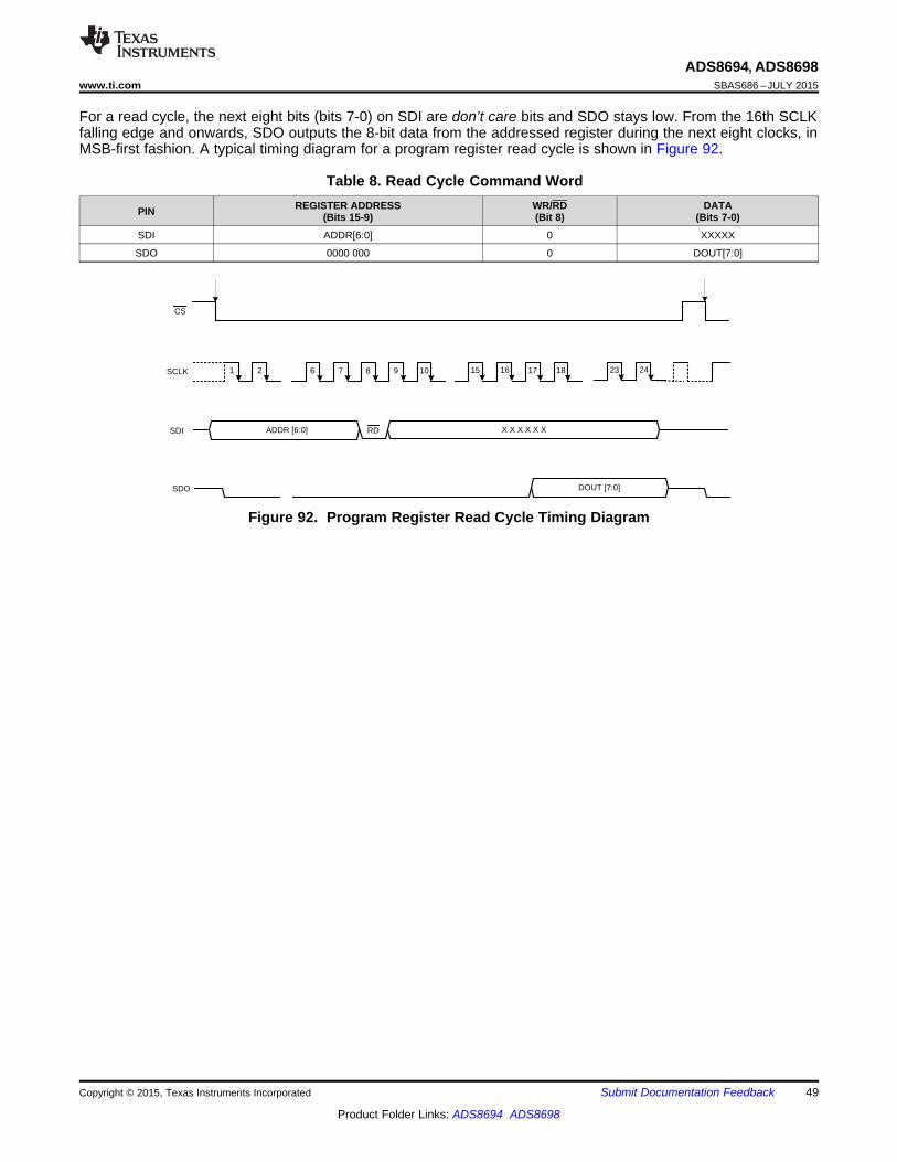
1 2 15 16SCLK
CS
SDO
ADDR [6:0] RD X X X X X XSDI
9 106 7 8
DOUT [7:0]
23 2417 18
ADS8694, ADS8698www.ti.com SBAS686 –JULY 2015
For a read cycle, the next eight bits (bits 7-0) on SDI are don’t care bits and SDO stays low. From the 16th SCLKfalling edge and onwards, SDO outputs the 8-bit data from the addressed register during the next eight clocks, inMSB-first fashion. A typical timing diagram for a program register read cycle is shown in Figure 92.
Table 8. Read Cycle Command WordREGISTER ADDRESS WR/RD DATAPIN (Bits 15-9) (Bit 8) (Bits 7-0)
SDI ADDR[6:0] 0 XXXXX
SDO 0000 000 0 DOUT[7:0]
Figure 92. Program Register Read Cycle Timing Diagram
Copyright © 2015, Texas Instruments Incorporated Submit Documentation Feedback 49
Product Folder Links: ADS8694 ADS8698
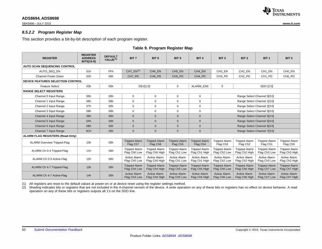
ADS8694, ADS8698SBAS686 –JULY 2015 www.ti.com
8.5.2.2 Program Register MapThis section provides a bit-by-bit description of each program register.
Table 9. Program Register MapREGISTER DEFAULTREGISTER ADDRESS BIT 7 BIT 6 BIT 5 BIT 4 BIT 3 BIT 2 BIT 1 BIT 0VALUE (1)BITS[15:9]
AUTO SCAN SEQUENCING CONTROL
AUTO_SEQ_EN 01h FFh CH7_EN (2) CH6_EN CH5_EN CH4_EN CH3_EN CH2_EN CH1_EN CH0_EN
Channel Power Down 02h 00h CH7_PD CH6_PD CH5_PD CH4_PD CH3_PD CH2_PD CH1_PD CH0_PD
DEVICE FEATURES SELECTION CONTROL
Feature Select 03h 00h DEV[1:0] 0 ALARM_EN0 0 SDO [2:0]
RANGE SELECT REGISTERS
Channel 0 Input Range 05h 00h 0 0 0 0 Range Select Channel 0[3:0]
Channel 1 Input Range 06h 00h 0 0 0 0 Range Select Channel 1[3:0]
Channel 2 Input Range 07h 00h 0 0 0 0 Range Select Channel 2[3:0]
Channel 3 Input Range 08h 00h 0 0 0 0 Range Select Channel 3[3:0]
Channel 4 Input Range 09h 00h 0 0 0 0 Range Select Channel 4[3:0]
Channel 5 Input Range 0Ah 00h 0 0 0 0 Range Select Channel 5[3:0]
Channel 6 Input Range 0Bh 00h 0 0 0 0 Range Select Channel 6[3:0]
Channel 7 Input Range 0Ch 00h 0 0 0 0 Range Select Channel 7[3:0]
ALARM FLAG REGISTERS (Read-Only)
Tripped Alarm Tripped Alarm Tripped Alarm Tripped Alarm Tripped Alarm Tripped Alarm Tripped Alarm Tripped AlarmALARM Overview Tripped-Flag 10h 00h Flag Ch7 Flag Ch6 Flag Ch5 Flag Ch4 Flag Ch3 Flag Ch2 Flag Ch1 Flag Ch0
Tripped Alarm Tripped Alarm Tripped Alarm Tripped Alarm Tripped Alarm Tripped Alarm Tripped Alarm Tripped AlarmALARM Ch 0-3 Tripped-Flag 11h 00h Flag Ch0 Low Flag Ch0 High Flag Ch1 Low Flag Ch1 High Flag Ch2 Low Flag Ch2 High Flag Ch3 Low Flag Ch3 High
Active Alarm Active Alarm Active Alarm Active Alarm Active Alarm Active Alarm Active Alarm Active AlarmALARM Ch 0-3 Active-Flag 12h 00h Flag Ch0 Low Flag Ch0 High Flag Ch1 Low Flag Ch1 High Flag Ch2 Low Flag Ch2 High Flag Ch3 Low Flag Ch3 High
Tripped Alarm Tripped Alarm Tripped Alarm Tripped Alarm Tripped Alarm Tripped Alarm Tripped Alarm Tripped AlarmALARM Ch 4-7 Tripped-Flag 13h 00h Flag Ch4 Low Flag Ch4 High Flag Ch5 Low Flag Ch5 High Flag Ch6 Low Flag Ch6 High Flag Ch7 Low Flag Ch7 High
Active Alarm Active Alarm Active Alarm Active Alarm Active Alarm Active Alarm Active Alarm Active AlarmALARM Ch 4-7 Active-Flag 14h 00h Flag Ch4 Low Flag Ch4 High Flag Ch5 Low Flag Ch5 High Flag Ch6 Low Flag Ch6 High Flag Ch7 Low Flag Ch7 High
(1) All registers are reset to the default values at power-on or at device reset using the register settings method.(2) Shading indicates bits or registers that are not included in the 4-channel version of the device. A write operation on any of these bits or registers has no effect on device behavior. A read
operation on any of these bits or registers outputs all 1's on the SDO line.
50 Submit Documentation Feedback Copyright © 2015, Texas Instruments Incorporated
Product Folder Links: ADS8694 ADS8698
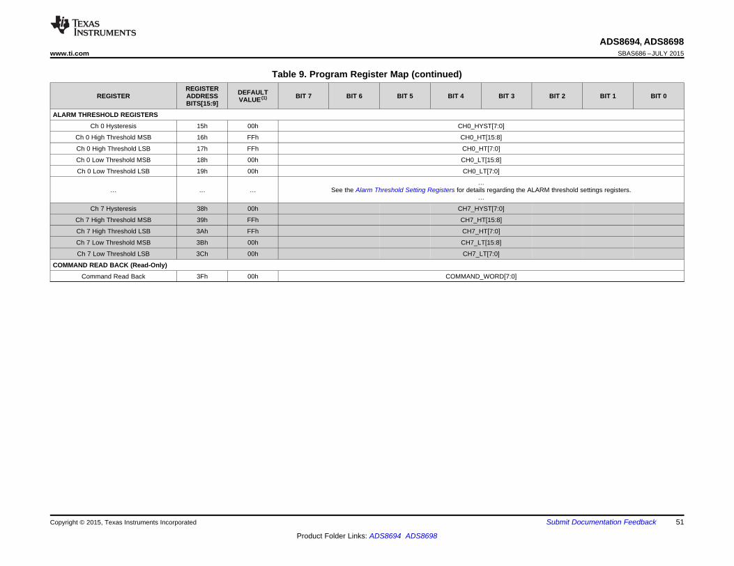
ADS8694, ADS8698www.ti.com SBAS686 –JULY 2015
Table 9. Program Register Map (continued)REGISTER DEFAULTREGISTER ADDRESS BIT 7 BIT 6 BIT 5 BIT 4 BIT 3 BIT 2 BIT 1 BIT 0VALUE (1)BITS[15:9]
ALARM THRESHOLD REGISTERS
Ch 0 Hysteresis 15h 00h CH0_HYST[7:0]
Ch 0 High Threshold MSB 16h FFh CH0_HT[15:8]
Ch 0 High Threshold LSB 17h FFh CH0_HT[7:0]
Ch 0 Low Threshold MSB 18h 00h CH0_LT[15:8]
Ch 0 Low Threshold LSB 19h 00h CH0_LT[7:0]
…… … … See the Alarm Threshold Setting Registers for details regarding the ALARM threshold settings registers.
…
Ch 7 Hysteresis 38h 00h CH7_HYST[7:0]
Ch 7 High Threshold MSB 39h FFh CH7_HT[15:8]
Ch 7 High Threshold LSB 3Ah FFh CH7_HT[7:0]
Ch 7 Low Threshold MSB 3Bh 00h CH7_LT[15:8]
Ch 7 Low Threshold LSB 3Ch 00h CH7_LT[7:0]
COMMAND READ BACK (Read-Only)
Command Read Back 3Fh 00h COMMAND_WORD[7:0]
Copyright © 2015, Texas Instruments Incorporated Submit Documentation Feedback 51
Product Folder Links: ADS8694 ADS8698
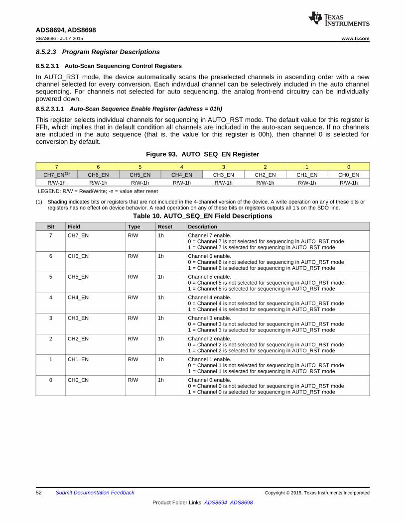
ADS8694, ADS8698SBAS686 –JULY 2015 www.ti.com
8.5.2.3 Program Register Descriptions
8.5.2.3.1 Auto-Scan Sequencing Control Registers
In AUTO_RST mode, the device automatically scans the preselected channels in ascending order with a newchannel selected for every conversion. Each individual channel can be selectively included in the auto channelsequencing. For channels not selected for auto sequencing, the analog front-end circuitry can be individuallypowered down.8.5.2.3.1.1 Auto-Scan Sequence Enable Register (address = 01h)
This register selects individual channels for sequencing in AUTO_RST mode. The default value for this register isFFh, which implies that in default condition all channels are included in the auto-scan sequence. If no channelsare included in the auto sequence (that is, the value for this register is 00h), then channel 0 is selected forconversion by default.
Figure 93. AUTO_SEQ_EN Register
7 6 5 4 3 2 1 0CH7_EN (1) CH6_EN CH5_EN CH4_EN CH3_EN CH2_EN CH1_EN CH0_EN
R/W-1h R/W-1h R/W-1h R/W-1h R/W-1h R/W-1h R/W-1h R/W-1hLEGEND: R/W = Read/Write; -n = value after reset
(1) Shading indicates bits or registers that are not included in the 4-channel version of the device. A write operation on any of these bits orregisters has no effect on device behavior. A read operation on any of these bits or registers outputs all 1's on the SDO line.
Table 10. AUTO_SEQ_EN Field DescriptionsBit Field Type Reset Description7 CH7_EN R/W 1h Channel 7 enable.
0 = Channel 7 is not selected for sequencing in AUTO_RST mode1 = Channel 7 is selected for sequencing in AUTO_RST mode
6 CH6_EN R/W 1h Channel 6 enable.0 = Channel 6 is not selected for sequencing in AUTO_RST mode1 = Channel 6 is selected for sequencing in AUTO_RST mode
5 CH5_EN R/W 1h Channel 5 enable.0 = Channel 5 is not selected for sequencing in AUTO_RST mode1 = Channel 5 is selected for sequencing in AUTO_RST mode
4 CH4_EN R/W 1h Channel 4 enable.0 = Channel 4 is not selected for sequencing in AUTO_RST mode1 = Channel 4 is selected for sequencing in AUTO_RST mode
3 CH3_EN R/W 1h Channel 3 enable.0 = Channel 3 is not selected for sequencing in AUTO_RST mode1 = Channel 3 is selected for sequencing in AUTO_RST mode
2 CH2_EN R/W 1h Channel 2 enable.0 = Channel 2 is not selected for sequencing in AUTO_RST mode1 = Channel 2 is selected for sequencing in AUTO_RST mode
1 CH1_EN R/W 1h Channel 1 enable.0 = Channel 1 is not selected for sequencing in AUTO_RST mode1 = Channel 1 is selected for sequencing in AUTO_RST mode
0 CH0_EN R/W 1h Channel 0 enable.0 = Channel 0 is not selected for sequencing in AUTO_RST mode1 = Channel 0 is selected for sequencing in AUTO_RST mode
52 Submit Documentation Feedback Copyright © 2015, Texas Instruments Incorporated
Product Folder Links: ADS8694 ADS8698
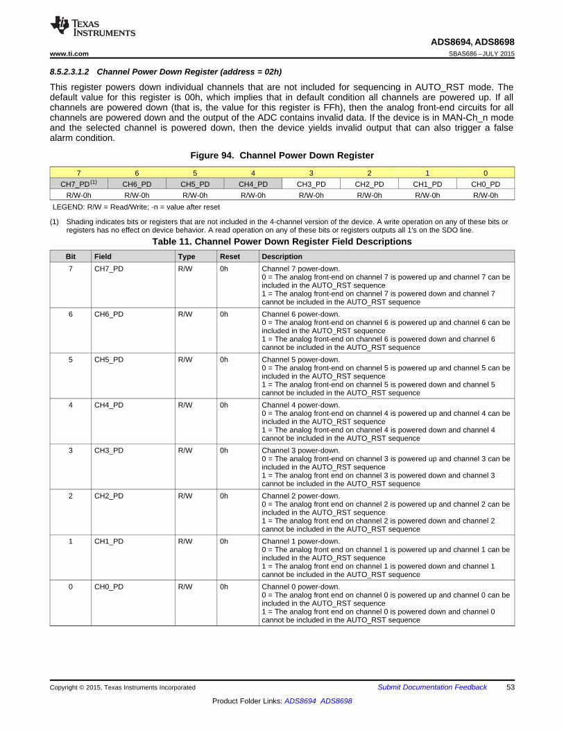
ADS8694, ADS8698www.ti.com SBAS686 –JULY 2015
8.5.2.3.1.2 Channel Power Down Register (address = 02h)
This register powers down individual channels that are not included for sequencing in AUTO_RST mode. Thedefault value for this register is 00h, which implies that in default condition all channels are powered up. If allchannels are powered down (that is, the value for this register is FFh), then the analog front-end circuits for allchannels are powered down and the output of the ADC contains invalid data. If the device is in MAN-Ch_n modeand the selected channel is powered down, then the device yields invalid output that can also trigger a falsealarm condition.
Figure 94. Channel Power Down Register
7 6 5 4 3 2 1 0CH7_PD (1) CH6_PD CH5_PD CH4_PD CH3_PD CH2_PD CH1_PD CH0_PD
R/W-0h R/W-0h R/W-0h R/W-0h R/W-0h R/W-0h R/W-0h R/W-0hLEGEND: R/W = Read/Write; -n = value after reset
(1) Shading indicates bits or registers that are not included in the 4-channel version of the device. A write operation on any of these bits orregisters has no effect on device behavior. A read operation on any of these bits or registers outputs all 1's on the SDO line.
Table 11. Channel Power Down Register Field DescriptionsBit Field Type Reset Description7 CH7_PD R/W 0h Channel 7 power-down.
0 = The analog front-end on channel 7 is powered up and channel 7 can beincluded in the AUTO_RST sequence1 = The analog front-end on channel 7 is powered down and channel 7cannot be included in the AUTO_RST sequence
6 CH6_PD R/W 0h Channel 6 power-down.0 = The analog front-end on channel 6 is powered up and channel 6 can beincluded in the AUTO_RST sequence1 = The analog front-end on channel 6 is powered down and channel 6cannot be included in the AUTO_RST sequence
5 CH5_PD R/W 0h Channel 5 power-down.0 = The analog front-end on channel 5 is powered up and channel 5 can beincluded in the AUTO_RST sequence1 = The analog front-end on channel 5 is powered down and channel 5cannot be included in the AUTO_RST sequence
4 CH4_PD R/W 0h Channel 4 power-down.0 = The analog front-end on channel 4 is powered up and channel 4 can beincluded in the AUTO_RST sequence1 = The analog front-end on channel 4 is powered down and channel 4cannot be included in the AUTO_RST sequence
3 CH3_PD R/W 0h Channel 3 power-down.0 = The analog front-end on channel 3 is powered up and channel 3 can beincluded in the AUTO_RST sequence1 = The analog front end on channel 3 is powered down and channel 3cannot be included in the AUTO_RST sequence
2 CH2_PD R/W 0h Channel 2 power-down.0 = The analog front end on channel 2 is powered up and channel 2 can beincluded in the AUTO_RST sequence1 = The analog front end on channel 2 is powered down and channel 2cannot be included in the AUTO_RST sequence
1 CH1_PD R/W 0h Channel 1 power-down.0 = The analog front end on channel 1 is powered up and channel 1 can beincluded in the AUTO_RST sequence1 = The analog front end on channel 1 is powered down and channel 1cannot be included in the AUTO_RST sequence
0 CH0_PD R/W 0h Channel 0 power-down.0 = The analog front end on channel 0 is powered up and channel 0 can beincluded in the AUTO_RST sequence1 = The analog front end on channel 0 is powered down and channel 0cannot be included in the AUTO_RST sequence
Copyright © 2015, Texas Instruments Incorporated Submit Documentation Feedback 53
Product Folder Links: ADS8694 ADS8698
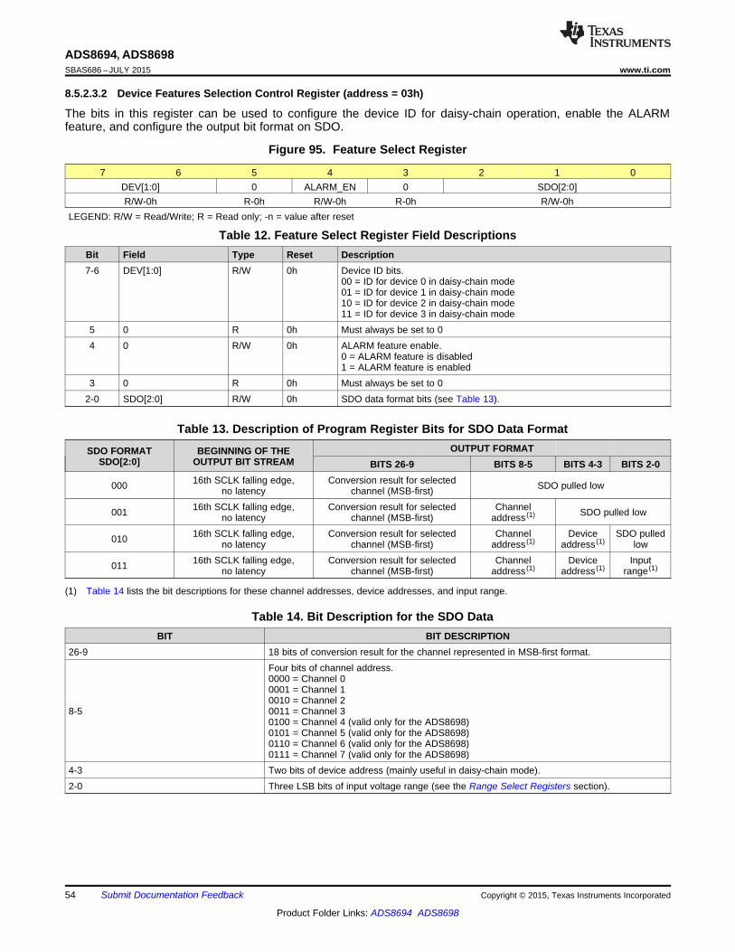
ADS8694, ADS8698SBAS686 –JULY 2015 www.ti.com
8.5.2.3.2 Device Features Selection Control Register (address = 03h)
The bits in this register can be used to configure the device ID for daisy-chain operation, enable the ALARMfeature, and configure the output bit format on SDO.
Figure 95. Feature Select Register
7 6 5 4 3 2 1 0DEV[1:0] 0 ALARM_EN 0 SDO[2:0]R/W-0h R-0h R/W-0h R-0h R/W-0h
LEGEND: R/W = Read/Write; R = Read only; -n = value after reset
Table 12. Feature Select Register Field DescriptionsBit Field Type Reset Description7-6 DEV[1:0] R/W 0h Device ID bits.
00 = ID for device 0 in daisy-chain mode01 = ID for device 1 in daisy-chain mode10 = ID for device 2 in daisy-chain mode11 = ID for device 3 in daisy-chain mode
5 0 R 0h Must always be set to 04 0 R/W 0h ALARM feature enable.
0 = ALARM feature is disabled1 = ALARM feature is enabled
3 0 R 0h Must always be set to 02-0 SDO[2:0] R/W 0h SDO data format bits (see Table 13).
Table 13. Description of Program Register Bits for SDO Data FormatOUTPUT FORMATSDO FORMAT BEGINNING OF THE
SDO[2:0] OUTPUT BIT STREAM BITS 26-9 BITS 8-5 BITS 4-3 BITS 2-016th SCLK falling edge, Conversion result for selected000 SDO pulled lowno latency channel (MSB-first)16th SCLK falling edge, Conversion result for selected Channel001 SDO pulled lowno latency channel (MSB-first) address (1)
16th SCLK falling edge, Conversion result for selected Channel Device SDO pulled010 no latency channel (MSB-first) address (1) address (1) low16th SCLK falling edge, Conversion result for selected Channel Device Input011 no latency channel (MSB-first) address (1) address (1) range (1)
(1) Table 14 lists the bit descriptions for these channel addresses, device addresses, and input range.
Table 14. Bit Description for the SDO DataBIT BIT DESCRIPTION
26-9 18 bits of conversion result for the channel represented in MSB-first format.Four bits of channel address.0000 = Channel 00001 = Channel 10010 = Channel 2
8-5 0011 = Channel 30100 = Channel 4 (valid only for the ADS8698)0101 = Channel 5 (valid only for the ADS8698)0110 = Channel 6 (valid only for the ADS8698)0111 = Channel 7 (valid only for the ADS8698)
4-3 Two bits of device address (mainly useful in daisy-chain mode).2-0 Three LSB bits of input voltage range (see the Range Select Registers section).
54 Submit Documentation Feedback Copyright © 2015, Texas Instruments Incorporated
Product Folder Links: ADS8694 ADS8698
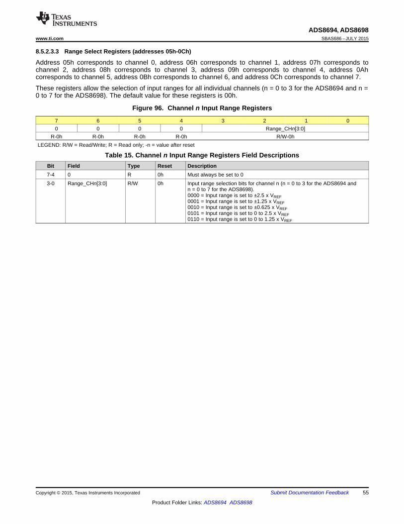
ADS8694, ADS8698www.ti.com SBAS686 –JULY 2015
8.5.2.3.3 Range Select Registers (addresses 05h-0Ch)
Address 05h corresponds to channel 0, address 06h corresponds to channel 1, address 07h corresponds tochannel 2, address 08h corresponds to channel 3, address 09h corresponds to channel 4, address 0Ahcorresponds to channel 5, address 0Bh corresponds to channel 6, and address 0Ch corresponds to channel 7.
These registers allow the selection of input ranges for all individual channels (n = 0 to 3 for the ADS8694 and n =0 to 7 for the ADS8698). The default value for these registers is 00h.
Figure 96. Channel n Input Range Registers
7 6 5 4 3 2 1 00 0 0 0 Range_CHn[3:0]
R-0h R-0h R-0h R-0h R/W-0hLEGEND: R/W = Read/Write; R = Read only; -n = value after reset
Table 15. Channel n Input Range Registers Field DescriptionsBit Field Type Reset Description7-4 0 R 0h Must always be set to 03-0 Range_CHn[3:0] R/W 0h Input range selection bits for channel n (n = 0 to 3 for the ADS8694 and
n = 0 to 7 for the ADS8698).0000 = Input range is set to ±2.5 x VREF0001 = Input range is set to ±1.25 x VREF0010 = Input range is set to ±0.625 x VREF0101 = Input range is set to 0 to 2.5 x VREF0110 = Input range is set to 0 to 1.25 x VREF
Copyright © 2015, Texas Instruments Incorporated Submit Documentation Feedback 55
Product Folder Links: ADS8694 ADS8698
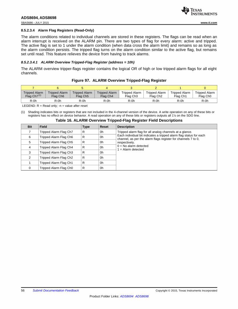
ADS8694, ADS8698SBAS686 –JULY 2015 www.ti.com
8.5.2.3.4 Alarm Flag Registers (Read-Only)
The alarm conditions related to individual channels are stored in these registers. The flags can be read when analarm interrupt is received on the ALARM pin. There are two types of flag for every alarm: active and tripped.The active flag is set to 1 under the alarm condition (when data cross the alarm limit) and remains so as long asthe alarm condition persists. The tripped flag turns on the alarm condition similar to the active flag, but remainsset until read. This feature relieves the device from having to track alarms.
8.5.2.3.4.1 ALARM Overview Tripped-Flag Register (address = 10h)
The ALARM overview tripper-flags register contains the logical OR of high or low tripped alarm flags for all eightchannels.
Figure 97. ALARM Overview Tripped-Flag Register
7 6 5 4 3 2 1 0Tripped Alarm Tripped Alarm Tripped Alarm Tripped Alarm Tripped Alarm Tripped Alarm Tripped Alarm Tripped Alarm
Flag Ch7 (1) Flag Ch6 Flag Ch5 Flag Ch4 Flag Ch3 Flag Ch2 Flag Ch1 Flag Ch0R-0h R-0h R-0h R-0h R-0h R-0h R-0h R-0h
LEGEND: R = Read only; -n = value after reset
(1) Shading indicates bits or registers that are not included in the 4-channel version of the device. A write operation on any of these bits orregisters has no effect on device behavior. A read operation on any of these bits or registers outputs all 1's on the SDO line.
Table 16. ALARM Overview Tripped-Flag Register Field DescriptionsBit Field Type Reset Description7 Tripped Alarm Flag Ch7 R 0h Tripped alarm flag for all analog channels at a glance.
Each individual bit indicates a tripped alarm flag status for each6 Tripped Alarm Flag Ch6 R 0h channel, as per the alarm flags register for channels 7 to 0,5 Tripped Alarm Flag Ch5 R 0h respectively.
0 = No alarm detected4 Tripped Alarm Flag Ch4 R 0h1 = Alarm detected
3 Tripped Alarm Flag Ch3 R 0h2 Tripped Alarm Flag Ch2 R 0h1 Tripped Alarm Flag Ch1 R 0h0 Tripped Alarm Flag Ch0 R 0h
56 Submit Documentation Feedback Copyright © 2015, Texas Instruments Incorporated
Product Folder Links: ADS8694 ADS8698
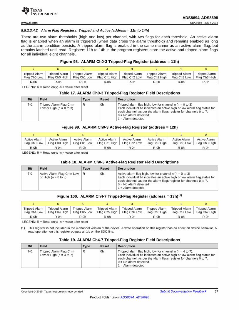
ADS8694, ADS8698www.ti.com SBAS686 –JULY 2015
8.5.2.3.4.2 Alarm Flag Registers: Tripped and Active (address = 11h to 14h)
There are two alarm thresholds (high and low) per channel, with two flags for each threshold. An active alarmflag is enabled when an alarm is triggered (when data cross the alarm threshold) and remains enabled as longas the alarm condition persists. A tripped alarm flag is enabled in the same manner as an active alarm flag, butremains latched until read. Registers 11h to 14h in the program registers store the active and tripped alarm flagsfor all individual eight channels.
Figure 98. ALARM Ch0-3 Tripped-Flag Register (address = 11h)
7 6 5 4 3 2 1 0Tripped Alarm Tripped Alarm Tripped Alarm Tripped Alarm Tripped Alarm Tripped Alarm Tripped Alarm Tripped AlarmFlag Ch0 Low Flag Ch0 High Flag Ch1 Low Flag Ch1 High Flag Ch2 Low Flag Ch2 High Flag Ch3 Low Flag Ch3 High
R-0h R-0h R-0h R-0h R-0h R-0h R-0h R-0hLEGEND: R = Read only; -n = value after reset
Table 17. ALARM Ch0-3 Tripped-Flag Register Field DescriptionsBit Field Type Reset Description7-0 Tripped Alarm Flag Ch n R 0h Tripped alarm flag high, low for channel n (n = 0 to 3)
Low or High (n = 0 to 3) Each individual bit indicates an active high or low alarm flag status foreach channel, as per the alarm flags register for channels 0 to 7.0 = No alarm detected1 = Alarm detected
Figure 99. ALARM Ch0-3 Active-Flag Register (address = 12h)
7 6 5 4 3 2 1 0Active Alarm Active Alarm Active Alarm Active Alarm Active Alarm Active Alarm Active Alarm Active Alarm
Flag Ch0 Low Flag Ch0 High Flag Ch1 Low Flag Ch1 High Flag Ch2 Low Flag Ch2 High Flag Ch3 Low Flag Ch3 HighR-0h R-0h R-0h R-0h R-0h R-0h R-0h R-0h
LEGEND: R = Read only; -n = value after reset
Table 18. ALARM Ch0-3 Active-Flag Register Field DescriptionsBit Field Type Reset Description7-0 Active Alarm Flag Ch n Low R 0h Active alarm flag high, low for channel n (n = 0 to 3)
or High (n = 0 to 3) Each individual bit indicates an active high or low alarm flag status foreach channel, as per the alarm flags register for channels 0 to 7.0 = No alarm detected1 = Alarm detected
Figure 100. ALARM Ch4-7 Tripped-Flag Register (address = 13h) (1)
7 6 5 4 3 2 1 0Tripped Alarm Tripped Alarm Tripped Alarm Tripped Alarm Tripped Alarm Tripped Alarm Tripped Alarm Tripped AlarmFlag Ch4 Low Flag Ch4 High Flag Ch5 Low Flag Ch5 High Flag Ch6 Low Flag Ch6 High Flag Ch7 Low Flag Ch7 High
R-0h R-0h R-0h R-0h R-0h R-0h R-0h R-0hLEGEND: R = Read only; -n = value after reset
(1) This register is not included in the 4-channel version of the device. A write operation on this register has no effect on device behavior. Aread operation on this register outputs all 1's on the SDO line.
Table 19. ALARM Ch4-7 Tripped-Flag Register Field DescriptionsBit Field Type Reset Description7-0 Tripped Alarm Flag Ch n R 0h Tripped alarm flag high, low for channel n (n = 4 to 7).
Low or High (n = 4 to 7) Each individual bit indicates an active high or low alarm flag status foreach channel, as per the alarm flags register for channels 0 to 7.0 = No alarm detected1 = Alarm detected
Copyright © 2015, Texas Instruments Incorporated Submit Documentation Feedback 57
Product Folder Links: ADS8694 ADS8698
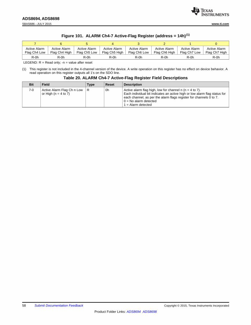
ADS8694, ADS8698SBAS686 –JULY 2015 www.ti.com
Figure 101. ALARM Ch4-7 Active-Flag Register (address = 14h) (1)
7 6 5 4 3 2 1 0Active Alarm Active Alarm Active Alarm Active Alarm Active Alarm Active Alarm Active Alarm Active Alarm
Flag Ch4 Low Flag Ch4 High Flag Ch5 Low Flag Ch5 High Flag Ch6 Low Flag Ch6 High Flag Ch7 Low Flag Ch7 HighR-0h R-0h R-0h R-0h R-0h R-0h R-0h R-0h
LEGEND: R = Read only; -n = value after reset
(1) This register is not included in the 4-channel version of the device. A write operation on this register has no effect on device behavior. Aread operation on this register outputs all 1's on the SDO line.
Table 20. ALARM Ch4-7 Active-Flag Register Field DescriptionsBit Field Type Reset Description7-0 Active Alarm Flag Ch n Low R 0h Active alarm flag high, low for channel n (n = 4 to 7).
or High (n = 4 to 7) Each individual bit indicates an active high or low alarm flag status foreach channel, as per the alarm flags register for channels 0 to 7.0 = No alarm detected1 = Alarm detected
58 Submit Documentation Feedback Copyright © 2015, Texas Instruments Incorporated
Product Folder Links: ADS8694 ADS8698
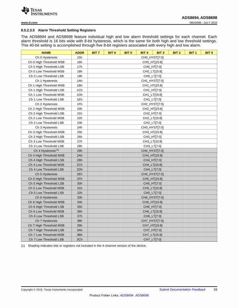
ADS8694, ADS8698www.ti.com SBAS686 –JULY 2015
8.5.2.3.5 Alarm Threshold Setting Registers
The ADS8694 and ADS8698 feature individual high and low alarm threshold settings for each channel. Eachalarm threshold is 16 bits wide with 8-bit hysteresis, which is the same for both high and low threshold settings.This 40-bit setting is accomplished through five 8-bit registers associated with every high and low alarm.
NAME ADDR BIT 7 BIT 6 BIT 5 BIT 4 BIT 3 BIT 2 BIT 1 BIT 0Ch 0 Hysteresis 15h CH0_HYST[7:0]
Ch 0 High Threshold MSB 16h CH0_HT[15:8]Ch 0 High Threshold LSB 17h CH0_HT[7:0]Ch 0 Low Threshold MSB 18h CH0_LT[15:8]Ch 0 Low Threshold LSB 19h CH0_LT[7:0]
Ch 1 Hysteresis 1Ah CH1_HYST[7:0]Ch 1 High Threshold MSB 1Bh CH1_HT[15:8]Ch 1 High Threshold LSB 1Ch CH1_HT[7:0]Ch 1 Low Threshold MSB 1Dh CH1_LT[15:8]Ch 1 Low Threshold LSB 1Eh CH1_LT[7:0]
Ch 2 Hysteresis 1Fh CH2_HYST[7:0]Ch 2 High Threshold MSB 20h CH2_HT[15:8]Ch 2 High Threshold LSB 21h CH2_HT[7:0]Ch 2 Low Threshold MSB 22h CH2_LT[15:8]Ch 2 Low Threshold LSB 23h CH2_LT[7:0]
Ch 3 Hysteresis 24h CH3_HYST[7:0]Ch 3 High Threshold MSB 25h CH3_HT[15:8]Ch 3 High Threshold LSB 26h CH3_HT[7:0]Ch 3 Low Threshold MSB 27h CH3_LT[15:8]Ch 3 Low Threshold LSB 28h CH3_LT[7:0]
Ch 4 Hysteresis (1) 29h CH4_HYST[7:0]Ch 4 High Threshold MSB 2Ah CH4_HT[15:8]Ch 4 High Threshold LSB 2Bh CH4_HT[7:0]Ch 4 Low Threshold MSB 2Ch CH4_LT[15:8]Ch 4 Low Threshold LSB 2Dh CH4_LT[7:0]
Ch 5 Hysteresis 2Eh CH5_HYST[7:0]Ch 5 High Threshold MSB 2Fh CH5_HT[15:8]Ch 5 High Threshold LSB 30h CH5_HT[7:0]Ch 5 Low Threshold MSB 31h CH5_LT[15:8]Ch 5 Low Threshold LSB 32h CH5_LT[7:0]
Ch 6 Hysteresis 33h CH6_HYST[7:0]Ch 6 High Threshold MSB 34h CH6_HT[15:8]Ch 6 High Threshold LSB 35h CH6_HT[7:0]Ch 6 Low Threshold MSB 36h CH6_LT[15:8]Ch 6 Low Threshold LSB 37h CH6_LT[7:0]
Ch 7 Hysteresis 38h CH7_HYST[7:0]Ch 7 High Threshold MSB 39h CH7_HT[15:8]Ch 7 High Threshold LSB 3Ah CH7_HT[7:0]Ch 7 Low Threshold MSB 3Bh CH7_LT[15:8]Ch 7 Low Threshold LSB 3Ch CH7_LT[7:0]
(1) Shading indicates bits or registers not included in the 4-channel version of the device.
Copyright © 2015, Texas Instruments Incorporated Submit Documentation Feedback 59
Product Folder Links: ADS8694 ADS8698
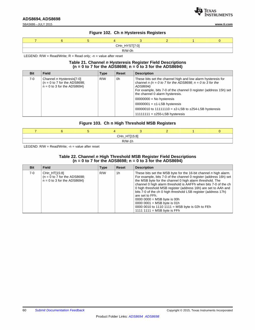
ADS8694, ADS8698SBAS686 –JULY 2015 www.ti.com
Figure 102. Ch n Hysteresis Registers
7 6 5 4 3 2 1 0CHn_HYST[7:0]
R/W-0hLEGEND: R/W = Read/Write; R = Read only; -n = value after reset
Table 21. Channel n Hysteresis Register Field Descriptions(n = 0 to 7 for the ADS8698; n = 0 to 3 for the ADS8694)
Bit Field Type Reset Description7-0 Channel n Hysteresis[7-0] R/W 0h These bits set the channel high and low alarm hysteresis for
(n = 0 to 7 for the ADS8698; channel n (n = 0 to 7 for the ADS8698; n = 0 to 3 for then = 0 to 3 for the ADS8694) ADS8694)
For example, bits 7-0 of the channel 0 register (address 15h) setthe channel 0 alarm hysteresis.00000000 = No hysteresis00000001 = ±1-LSB hysteresis00000010 to 11111110 = ±2-LSB to ±254-LSB hysteresis11111111 = ±255-LSB hysteresis
Figure 103. Ch n High Threshold MSB Registers
7 6 5 4 3 2 1 0CHn_HT[15:8]
R/W-1hLEGEND: R/W = Read/Write; -n = value after reset
Table 22. Channel n High Threshold MSB Register Field Descriptions(n = 0 to 7 for the ADS8698; n = 0 to 3 for the ADS8694)
Bit Field Type Reset Description7-0 CHn_HT[15:8] R/W 1h These bits set the MSB byte for the 16-bit channel n high alarm.
(n = 0 to 7 for the ADS8698; For example, bits 7-0 of the channel 0 register (address 16h) setn = 0 to 3 for the ADS8694) the MSB byte for the channel 0 high alarm threshold. The
channel 0 high alarm threshold is AAFFh when bits 7-0 of the ch0 high threshold MSB register (address 16h) are set to AAh andbits 7-0 of the ch 0 high threshold LSB register (address 17h)are set to FFh.0000 0000 = MSB byte is 00h0000 0001 = MSB byte is 01h0000 0010 to 1110 1111 = MSB byte is 02h to FEh1111 1111 = MSB byte is FFh
60 Submit Documentation Feedback Copyright © 2015, Texas Instruments Incorporated
Product Folder Links: ADS8694 ADS8698
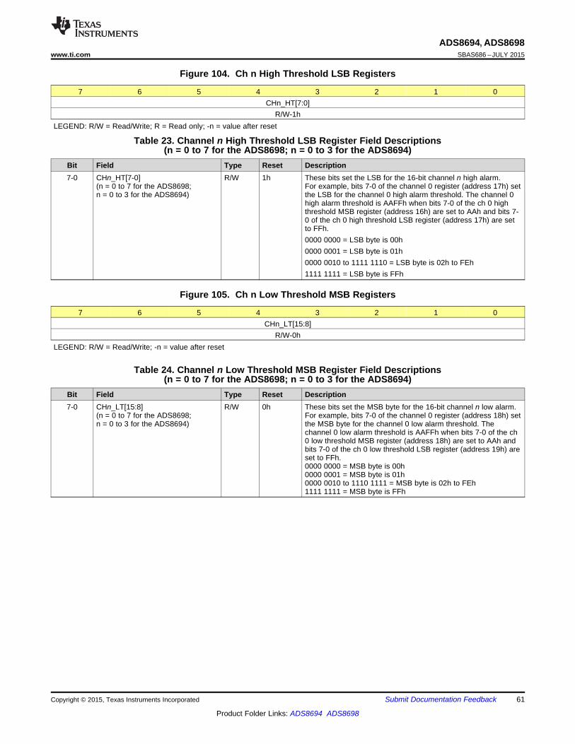
ADS8694, ADS8698www.ti.com SBAS686 –JULY 2015
Figure 104. Ch n High Threshold LSB Registers
7 6 5 4 3 2 1 0CHn_HT[7:0]
R/W-1hLEGEND: R/W = Read/Write; R = Read only; -n = value after reset
Table 23. Channel n High Threshold LSB Register Field Descriptions(n = 0 to 7 for the ADS8698; n = 0 to 3 for the ADS8694)
Bit Field Type Reset Description7-0 CHn_HT[7-0] R/W 1h These bits set the LSB for the 16-bit channel n high alarm.
(n = 0 to 7 for the ADS8698; For example, bits 7-0 of the channel 0 register (address 17h) setn = 0 to 3 for the ADS8694) the LSB for the channel 0 high alarm threshold. The channel 0
high alarm threshold is AAFFh when bits 7-0 of the ch 0 highthreshold MSB register (address 16h) are set to AAh and bits 7-0 of the ch 0 high threshold LSB register (address 17h) are setto FFh.0000 0000 = LSB byte is 00h0000 0001 = LSB byte is 01h0000 0010 to 1111 1110 = LSB byte is 02h to FEh1111 1111 = LSB byte is FFh
Figure 105. Ch n Low Threshold MSB Registers
7 6 5 4 3 2 1 0CHn_LT[15:8]
R/W-0hLEGEND: R/W = Read/Write; -n = value after reset
Table 24. Channel n Low Threshold MSB Register Field Descriptions(n = 0 to 7 for the ADS8698; n = 0 to 3 for the ADS8694)
Bit Field Type Reset Description7-0 CHn_LT[15:8] R/W 0h These bits set the MSB byte for the 16-bit channel n low alarm.
(n = 0 to 7 for the ADS8698; For example, bits 7-0 of the channel 0 register (address 18h) setn = 0 to 3 for the ADS8694) the MSB byte for the channel 0 low alarm threshold. The
channel 0 low alarm threshold is AAFFh when bits 7-0 of the ch0 low threshold MSB register (address 18h) are set to AAh andbits 7-0 of the ch 0 low threshold LSB register (address 19h) areset to FFh.0000 0000 = MSB byte is 00h0000 0001 = MSB byte is 01h0000 0010 to 1110 1111 = MSB byte is 02h to FEh1111 1111 = MSB byte is FFh
Copyright © 2015, Texas Instruments Incorporated Submit Documentation Feedback 61
Product Folder Links: ADS8694 ADS8698
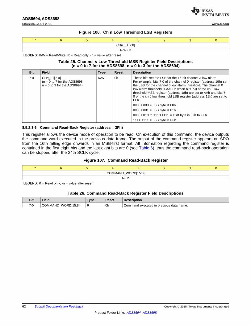
ADS8694, ADS8698SBAS686 –JULY 2015 www.ti.com
Figure 106. Ch n Low Threshold LSB Registers
7 6 5 4 3 2 1 0CHn_LT[7:0]
R/W-0hLEGEND: R/W = Read/Write; R = Read only; -n = value after reset
Table 25. Channel n Low Threshold MSB Register Field Descriptions(n = 0 to 7 for the ADS8698; n = 0 to 3 for the ADS8694)
Bit Field Type Reset Description7-0 CHn_LT[7-0] R/W 0h These bits set the LSB for the 16-bit channel n low alarm.
(n = 0 to 7 for the ADS8698; For example, bits 7-0 of the channel 0 register (address 19h) setn = 0 to 3 for the ADS8694) the LSB for the channel 0 low alarm threshold. The channel 0
low alarm threshold is AAFFh when bits 7-0 of the ch 0 lowthreshold MSB register (address 18h) are set to AAh and bits 7-0 of the ch 0 low threshold LSB register (address 19h) are set toFFh.0000 0000 = LSB byte is 00h0000 0001 = LSB byte is 01h0000 0010 to 1110 1111 = LSB byte is 02h to FEh1111 1111 = LSB byte is FFh
8.5.2.3.6 Command Read-Back Register (address = 3Fh)
This register allows the device mode of operation to be read. On execution of this command, the device outputsthe command word executed in the previous data frame. The output of the command register appears on SDOfrom the 16th falling edge onwards in an MSB-first format. All information regarding the command register iscontained in the first eight bits and the last eight bits are 0 (see Table 6), thus the command read-back operationcan be stopped after the 24th SCLK cycle.
Figure 107. Command Read-Back Register
7 6 5 4 3 2 1 0COMMAND_WORD[15:8]
R-0hLEGEND: R = Read only; -n = value after reset
Table 26. Command Read-Back Register Field DescriptionsBit Field Type Reset Description7-0 COMMAND_WORD[15:8] R 0h Command executed in previous data frame.
62 Submit Documentation Feedback Copyright © 2015, Texas Instruments Incorporated
Product Folder Links: ADS8694 ADS8698
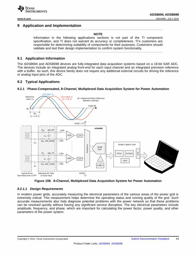
1 M:
1 M:
LPF
AIN_0P
AIN_0GND
4.096 V
AVDD = 5 V
ADS8698
18-Bit ADC
C0
R0P
R0M
Mul
tiple
xer
FPGA SITARA
DDR
US
B
Simple Capture Card
x
xx
x
xPhase
Compensation GUI
AGND
PGA
1 M:
1 M:
LPF
AIN_7P
AIN_7GND
C7
R7P
R7M
PGA
Typical 50-Hz Sine-Wave from CT/PT
Balanced RC Filter on Each Input
Angle (�)
¨�r1
¨�rn (n = 1 to 7)
Reference Input, VR
Ch1 Input, V1
Ch n Input, Vn
(n = 1 to 7) ¨��= Measured Phase Difference Between Channels
ADS8694, ADS8698www.ti.com SBAS686 –JULY 2015
9 Application and Implementation
NOTEInformation in the following applications sections is not part of the TI componentspecification, and TI does not warrant its accuracy or completeness. TI’s customers areresponsible for determining suitability of components for their purposes. Customers shouldvalidate and test their design implementation to confirm system functionality.
9.1 Application InformationThe ADS8694 and ADS8698 devices are fully-integrated data acquisition systems based on a 18-bit SAR ADC.The devices include an integrated analog front-end for each input channel and an integrated precision referencewith a buffer. As such, this device family does not require any additional external circuits for driving the referenceor analog input pins of the ADC.
9.2 Typical Applications
9.2.1 Phase-Compensated, 8-Channel, Multiplexed Data Acquisition System for Power Automation
Figure 108. 8-Channel, Multiplexed Data Acquisition System for Power Automation
9.2.1.1 Design RequirementsIn modern power grids, accurately measuring the electrical parameters of the various areas of the power grid isextremely critical. This measurement helps determine the operating status and running quality of the grid. Suchaccurate measurements also help diagnose potential problems with the power network so that these problemscan be resolved quickly without having any significant service disruption. The key electrical parameters includeamplitude, frequency, and phase, which are important for calculating the power factor, power quality, and otherparameters of the power system.
Copyright © 2015, Texas Instruments Incorporated Submit Documentation Feedback 63
Product Folder Links: ADS8694 ADS8698
ADS8694, ADS8698SBAS686 –JULY 2015 www.ti.com
Typical Applications (continued)The phase angle of the electrical signal on the power network buses is a special interest to power systemengineers. The primary objective for this design is to accurately measure the phase and phase differencebetween the analog input signals in a multichannel data acquisition system. When multiple input channels aresampled in a sequential manner as in a multiplexed ADC, an additional phase delay is introduced between thechannels. Thus, the phase measurements are not accurate. However, this additional phase delay is constant andcan be compensated in application software.
The key design requirements are given below:• Single-ended sinusoidal input signal with a ±10-V amplitude and typical frequency (fIN = 50 Hz).• Design an 8-channel multiplexed data acquisition system using a 18-bit SAR ADC.• Design a software algorithm to compensate for the additional phase difference between the channels.
9.2.1.2 Detailed Design ProcedureThe application circuit and system diagram for this design is shown in Figure 108. This design includes acomplete hardware and software implementation of a multichannel data acquisition system for power automationapplications.
This system can be designed using the ADS8698, which is a 18-bit, 500-kSPS, 8-channel, multiplexed input,SAR ADC with integrated precision reference and analog front-end circuitry for each channel. The ADC supportsbipolar input ranges up to ±10.24 V with a single 5-V supply and provides minimum latency in data outputresulting from the SAR architecture. The integration offered by this device makes the ADS8694 and ADS8698 anideal selection for such applications, because the integrated signal conditioning helps minimize systemcomponents and avoids the need for generating high-voltage supply rails. The overall system-level dc precision(gain and offset errors) and low temperature drift offered by this device helps system designers achieve thedesired system accuracy without calibration. In most applications, using passive RC filters or multi-stage filters infront of the ADC is preferred to reduce the noise of the input signal.
The software algorithm implemented in this design uses the discrete fourier transform (DFT) method to calculateand track the input signal frequency, obtain the exact phase angle of the individual signal, calculate the phasedifference, and implement phase compensation. The entire algorithm has four steps:• Calculate the theoretical phase difference introduced by the ADC resulting from multiplexing input channels.• Estimate the frequency of the input signal using frequency tracking and DFT techniques.• Calculate the phase angle of all signals in the system based on the estimated frequency.• Compensate the phase difference for all channels using the theoretical value of an additional MUX phase
delay calculated in the first step.
For a step-by-step design procedure, circuit schematics, bill of materials, PCB files, simulation results, and testresults, see Phase Compensated 8-Channel, Multiplexed Data Acquisition System for Power AutomationReference Design (TIDU427).
64 Submit Documentation Feedback Copyright © 2015, Texas Instruments Incorporated
Product Folder Links: ADS8694 ADS8698
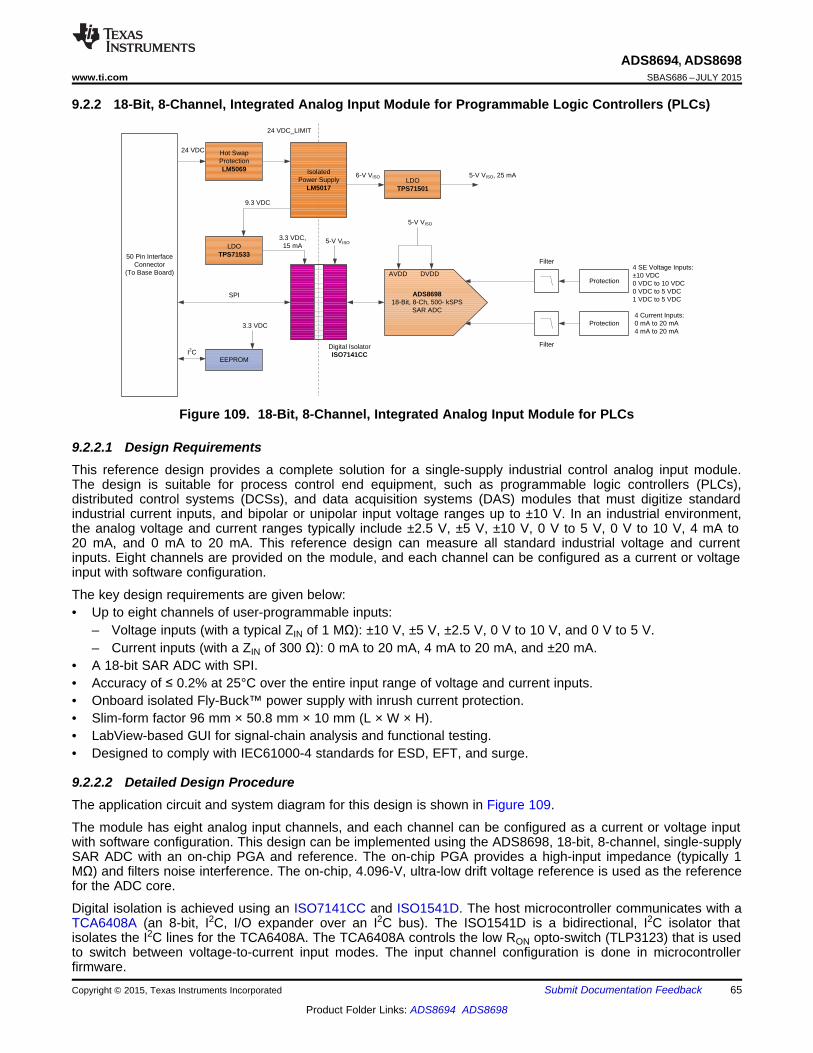
Hot Swap Protection LM5069
LDOTPS71501
LDOTPS71533
EEPROM
Isolated Power Supply
LM5017
Protection
Protection
Filter
Filter
4 SE Voltage Inputs:±10 VDC0 VDC to 10 VDC0 VDC to 5 VDC1 VDC to 5 VDC
4 Current Inputs:0 mA to 20 mA4 mA to 20 mA
ADS869818-Bit, 8-Ch, 500- kSPS
SAR ADC
AVDD DVDD
5-V VISO
5-V VISO
Digital IsolatorISO7141CC
3.3 VDC
I2C
3.3 VDC,15 mA
SPI
24 VDC
24 VDC_LIMIT
6-V VISO 5-V VISO, 25 mA
9.3 VDC
50 Pin InterfaceConnector
(To Base Board)
ADS8694, ADS8698www.ti.com SBAS686 –JULY 2015
9.2.2 18-Bit, 8-Channel, Integrated Analog Input Module for Programmable Logic Controllers (PLCs)
Figure 109. 18-Bit, 8-Channel, Integrated Analog Input Module for PLCs
9.2.2.1 Design RequirementsThis reference design provides a complete solution for a single-supply industrial control analog input module.The design is suitable for process control end equipment, such as programmable logic controllers (PLCs),distributed control systems (DCSs), and data acquisition systems (DAS) modules that must digitize standardindustrial current inputs, and bipolar or unipolar input voltage ranges up to ±10 V. In an industrial environment,the analog voltage and current ranges typically include ±2.5 V, ±5 V, ±10 V, 0 V to 5 V, 0 V to 10 V, 4 mA to20 mA, and 0 mA to 20 mA. This reference design can measure all standard industrial voltage and currentinputs. Eight channels are provided on the module, and each channel can be configured as a current or voltageinput with software configuration.
The key design requirements are given below:• Up to eight channels of user-programmable inputs:
– Voltage inputs (with a typical ZIN of 1 MΩ): ±10 V, ±5 V, ±2.5 V, 0 V to 10 V, and 0 V to 5 V.– Current inputs (with a ZIN of 300 Ω): 0 mA to 20 mA, 4 mA to 20 mA, and ±20 mA.
• A 18-bit SAR ADC with SPI.• Accuracy of ≤ 0.2% at 25°C over the entire input range of voltage and current inputs.• Onboard isolated Fly-Buck™ power supply with inrush current protection.• Slim-form factor 96 mm × 50.8 mm × 10 mm (L × W × H).• LabView-based GUI for signal-chain analysis and functional testing.• Designed to comply with IEC61000-4 standards for ESD, EFT, and surge.
9.2.2.2 Detailed Design ProcedureThe application circuit and system diagram for this design is shown in Figure 109.
The module has eight analog input channels, and each channel can be configured as a current or voltage inputwith software configuration. This design can be implemented using the ADS8698, 18-bit, 8-channel, single-supplySAR ADC with an on-chip PGA and reference. The on-chip PGA provides a high-input impedance (typically 1MΩ) and filters noise interference. The on-chip, 4.096-V, ultra-low drift voltage reference is used as the referencefor the ADC core.
Digital isolation is achieved using an ISO7141CC and ISO1541D. The host microcontroller communicates with aTCA6408A (an 8-bit, I2C, I/O expander over an I2C bus). The ISO1541D is a bidirectional, I2C isolator thatisolates the I2C lines for the TCA6408A. The TCA6408A controls the low RON opto-switch (TLP3123) that is usedto switch between voltage-to-current input modes. The input channel configuration is done in microcontrollerfirmware.
Copyright © 2015, Texas Instruments Incorporated Submit Documentation Feedback 65
Product Folder Links: ADS8694 ADS8698
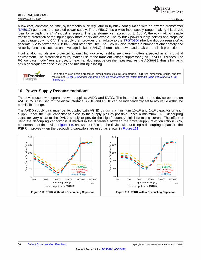
40
60
80
100
120
140
100 1000 10000 100000 1000000 10000000
Pow
er S
uppl
y R
ejec
tion
Rat
io
Input Frequency (Hz) C046
----- ± 2.5*VREF
----- ± 1.25*VREF ----- ± 0.625*VREF ------ +2.5*VREF ------+1.25*VREF
40
60
80
100
120
140
50 500 5000 50000 500000 5000000
Pow
er S
uppl
y R
ejec
tion
Rat
io
Input Frequency (Hz) C045
----- ± 2.5*VREF
----- ± 1.25*VREF ----- ± 0.625*VREF ------ +2.5*VREF ------+1.25*VREF
ADS8694, ADS8698SBAS686 –JULY 2015 www.ti.com
A low-cost, constant, on-time, synchronous buck regulator in fly-buck configuration with an external transformer(LM5017) generates the isolated power supply. The LM5017 has a wide input supply range, making this deviceideal for accepting a 24-V industrial supply. This transformer can accept up to 100 V, thereby making reliabletransient protection of the input supply more easily achievable. The fly-buck power supply isolates and steps theinput voltage down to 6 V. The supply then provides that voltage to the TPS70950 (the low dropout regulator) togenerate 5 V to power the ADS8698 and other circuitry. The LM5017 also features a number of other safety andreliability functions, such as undervoltage lockout (UVLO), thermal shutdown, and peak current limit protection.
Input analog signals are protected against high-voltage, fast-transient events often expected in an industrialenvironment. The protection circuitry makes use of the transient voltage suppressor (TVS) and ESD diodes. TheRC low-pass mode filters are used on each analog input before the input reaches the ADS8698, thus eliminatingany high-frequency noise pickups and minimizing aliasing.
For a step-by-step design procedure, circuit schematics, bill of materials, PCB files, simulation results, and testresults, see 16-Bit, 8-Channel, Integrated Analog Input Module for Programmable Logic Controllers (PLCs)(TIDU365).
10 Power-Supply RecommendationsThe device uses two separate power supplies: AVDD and DVDD. The internal circuits of the device operate onAVDD; DVDD is used for the digital interface. AVDD and DVDD can be independently set to any value within thepermissible range.
The AVDD supply pins must be decoupled with AGND by using a minimum 10-µF and 1-µF capacitor on eachsupply. Place the 1-µF capacitor as close to the supply pins as possible. Place a minimum 10-µF decouplingcapacitor very close to the DVDD supply to provide the high-frequency digital switching current. The effect ofusing the decoupling capacitor is illustrated in the difference between the power-supply rejection ratio (PSRR)performance of the device. Figure 110 shows the PSRR of the device without using a decoupling capacitor. ThePSRR improves when the decoupling capacitors are used, as shown in Figure 111.
Code output near 131072 Code output near 131072
Figure 110. PSRR Without a Decoupling Capacitor Figure 111. PSRR With a Decoupling Capacitor
66 Submit Documentation Feedback Copyright © 2015, Texas Instruments Incorporated
Product Folder Links: ADS8694 ADS8698
ADS8694, ADS8698www.ti.com SBAS686 –JULY 2015
11 Layout
11.1 Layout GuidelinesFigure 112 illustrates a PCB layout example for the ADS8694 and ADS8698.• Partition the PCB into analog and digital sections. Care must be taken to ensure that the analog signals are
kept away from the digital lines. This layout helps keep the analog input and reference input signals awayfrom the digital noise. In this layout example, the analog input and reference signals are routed on the lowerside of the board and the digital connections are routed on the top side of the board.
• Using a single dedicated ground plane is strongly encouraged.• Power sources to the ADS8694 and ADS8698 must be clean and well-bypassed. TI recommends using a
1-μF, X7R-grade, 0603-size ceramic capacitor with at least a 10-V rating in close proximity to the analog(AVDD) supply pins. For decoupling the digital (DVDD) supply pin, a 10-μF, X7R-grade, 0805-size ceramiccapacitor with at least a 10-V rating is recommended. Placing vias between the AVDD, DVDD pins and thebypass capacitors must be avoided. All ground pins must be connected to the ground plane using short, lowimpedance paths.
• There are two decoupling capacitors used for the REFCAP pin. The first is a small, 1-μF, X7R-grade, 0603-size ceramic capacitor placed close to the device pins for decoupling the high-frequency signals and thesecond is a 22-µF, X7R-grade, 1210-size ceramic capacitor to provide the charge required by the referencecircuit of the device. Both of these capacitors must be directly connected to the device pins without any viasbetween the pins and capacitors.
• The REFIO pin also must be decoupled with a 10-µF ceramic capacitor, if the internal reference of the deviceis used. The capacitor must be placed close to the device pins.
• For the auxiliary channel, the fly-wheel RC filter components must be placed close to the device. Amongceramic surface-mount capacitors, COG (NPO) ceramic capacitors provide the best capacitance precision.The type of dielectric used in COG (NPO) ceramic capacitors provides the most stable electrical propertiesover voltage, frequency, and temperature changes.
Copyright © 2015, Texas Instruments Incorporated Submit Documentation Feedback 67
Product Folder Links: ADS8694 ADS8698
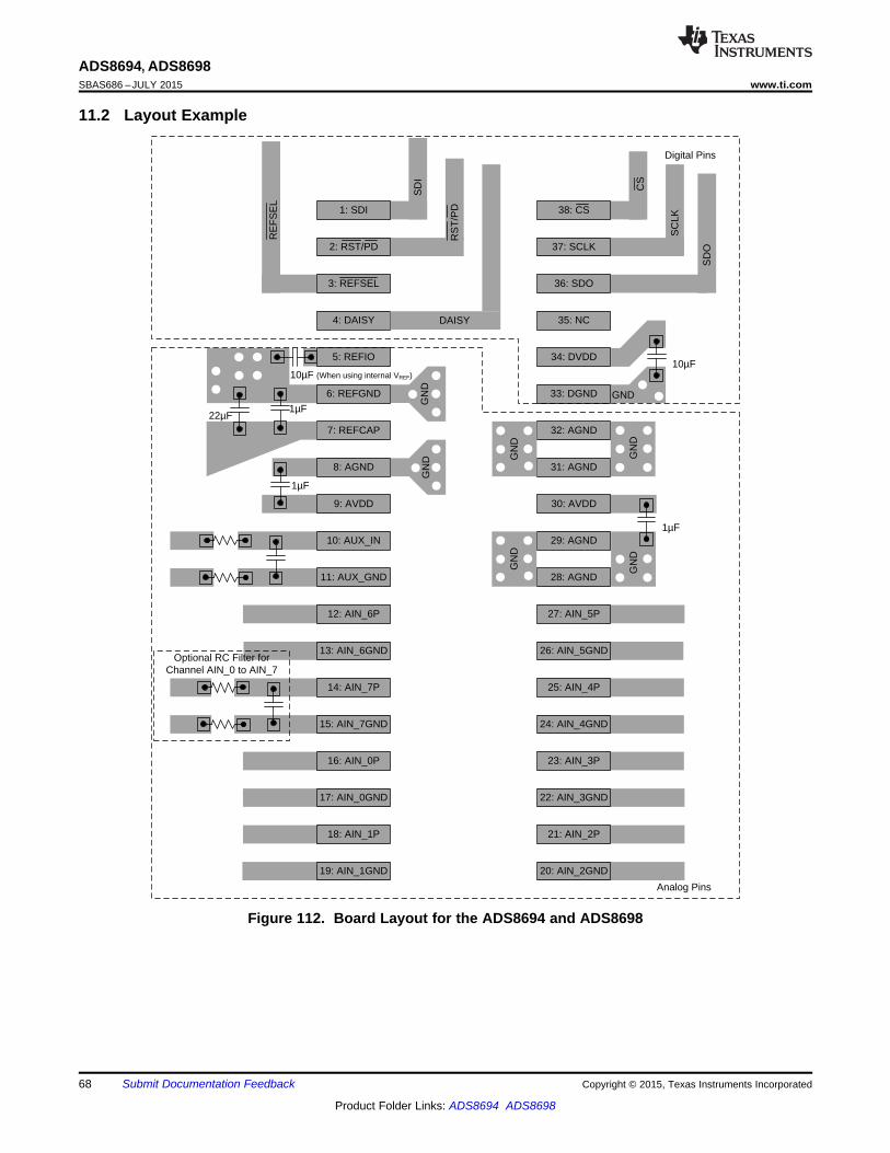
`
1: SDI
2: RST/PD
3: REFSEL
4: DAISY
5: REFIO
6: REFGND
7: REFCAP
8: AGND
9: AVDD
10: AUX_IN
11: AUX_GND
12: AIN_6P
13: AIN_6GND
14: AIN_7P
15: AIN_7GND
16: AIN_0P
17: AIN_0GND
18: AIN_1P
19: AIN_1GND
38: CS
37: SCLK
36: SDO
35: NC
34: DVDD
33: DGND
32: AGND
31: AGND
30: AVDD
29: AGND
28: AGND
27: AIN_5P
26: AIN_5GND
25: AIN_4P
24: AIN_4GND
23: AIN_3P
22: AIN_3GND
21: AIN_2P
20: AIN_2GND
1µF22µF
GN
DG
ND
GND
GN
DG
ND
10µF
GN
D
1µF
GN
DC
S
SC
LK
SD
O
SD
I
RS
T/P
D
RE
FS
EL
DAISY
Optional RC Filter for Channel AIN_0 to AIN_7
1µF
Digital Pins
Analog Pins
10µF (When using internal VREF)
ADS8694, ADS8698SBAS686 –JULY 2015 www.ti.com
11.2 Layout Example
Figure 112. Board Layout for the ADS8694 and ADS8698
68 Submit Documentation Feedback Copyright © 2015, Texas Instruments Incorporated
Product Folder Links: ADS8694 ADS8698
ADS8694, ADS8698www.ti.com SBAS686 –JULY 2015
12 Device and Documentation Support
12.1 Documentation Support
12.1.1 Related DocumentationFor related documentation see the following:• LM5017 Data Sheet, SNVS783• OPA320 Data Sheet, SBOS513• REF5040 Data Sheet, SBOS410F• AN-2029 - Handling & Process Recommendations, SNOA550B• TIDA-00164 Verified Design Reference Guide: 16-Bit, 8-Channel, Integrated Analog Input Module for
Programmable Logic Controllers (PLCs), TIDU365• TIPD167 Verified Design Reference Guide: Phase Compensated 8-Channel, Multiplexed Data Acquisition
System for Power Automation, TIDU427
12.2 Related LinksThe table below lists quick access links. Categories include technical documents, support and communityresources, tools and software, and quick access to sample or buy.
Table 27. Related LinksTECHNICAL TOOLS & SUPPORT &PARTS PRODUCT FOLDER SAMPLE & BUY DOCUMENTS SOFTWARE COMMUNITY
ADS8694 Click here Click here Click here Click here Click hereADS8698 Click here Click here Click here Click here Click here
12.3 Community ResourcesThe following links connect to TI community resources. Linked contents are provided "AS IS" by the respectivecontributors. They do not constitute TI specifications and do not necessarily reflect TI's views; see TI's Terms ofUse.
TI E2E™ Online Community TI's Engineer-to-Engineer (E2E) Community. Created to foster collaborationamong engineers. At e2e.ti.com, you can ask questions, share knowledge, explore ideas and helpsolve problems with fellow engineers.
Design Support TI's Design Support Quickly find helpful E2E forums along with design support tools andcontact information for technical support.
12.4 TrademarksE2E is a trademark of Texas Instruments.Fly-Buck is a trademark of Texas Instruments, Inc.SPI is a trademark of Motorola.All other trademarks are the property of their respective owners.
12.5 Electrostatic Discharge CautionThis integrated circuit can be damaged by ESD. Texas Instruments recommends that all integrated circuits be handled withappropriate precautions. Failure to observe proper handling and installation procedures can cause damage.
ESD damage can range from subtle performance degradation to complete device failure. Precision integrated circuits may be moresusceptible to damage because very small parametric changes could cause the device not to meet its published specifications.
12.6 GlossarySLYZ022 — TI Glossary.
This glossary lists and explains terms, acronyms, and definitions.
Copyright © 2015, Texas Instruments Incorporated Submit Documentation Feedback 69
Product Folder Links: ADS8694 ADS8698
ADS8694, ADS8698SBAS686 –JULY 2015 www.ti.com
13 Mechanical, Packaging, and Orderable InformationThe following pages include mechanical packaging and orderable information. This information is the mostcurrent data available for the designated devices. This data is subject to change without notice and revision ofthis document. For browser-based versions of this data sheet, refer to the left-hand navigation.
70 Submit Documentation Feedback Copyright © 2015, Texas Instruments Incorporated
Product Folder Links: ADS8694 ADS8698
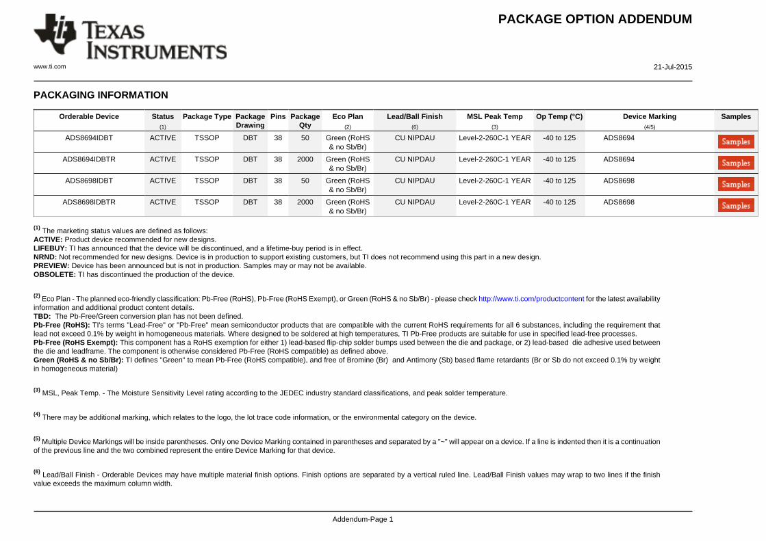
PACKAGE OPTION ADDENDUM
www.ti.com 21-Jul-2015
Addendum-Page 1
PACKAGING INFORMATION
Orderable Device Status(1)
Package Type PackageDrawing
Pins PackageQty
Eco Plan(2)
Lead/Ball Finish(6)
MSL Peak Temp(3)
Op Temp (°C) Device Marking(4/5)
Samples
ADS8694IDBT ACTIVE TSSOP DBT 38 50 Green (RoHS& no Sb/Br)
CU NIPDAU Level-2-260C-1 YEAR -40 to 125 ADS8694
ADS8694IDBTR ACTIVE TSSOP DBT 38 2000 Green (RoHS& no Sb/Br)
CU NIPDAU Level-2-260C-1 YEAR -40 to 125 ADS8694
ADS8698IDBT ACTIVE TSSOP DBT 38 50 Green (RoHS& no Sb/Br)
CU NIPDAU Level-2-260C-1 YEAR -40 to 125 ADS8698
ADS8698IDBTR ACTIVE TSSOP DBT 38 2000 Green (RoHS& no Sb/Br)
CU NIPDAU Level-2-260C-1 YEAR -40 to 125 ADS8698
(1) The marketing status values are defined as follows:ACTIVE: Product device recommended for new designs.LIFEBUY: TI has announced that the device will be discontinued, and a lifetime-buy period is in effect.NRND: Not recommended for new designs. Device is in production to support existing customers, but TI does not recommend using this part in a new design.PREVIEW: Device has been announced but is not in production. Samples may or may not be available.OBSOLETE: TI has discontinued the production of the device.
(2) Eco Plan - The planned eco-friendly classification: Pb-Free (RoHS), Pb-Free (RoHS Exempt), or Green (RoHS & no Sb/Br) - please check http://www.ti.com/productcontent for the latest availabilityinformation and additional product content details.TBD: The Pb-Free/Green conversion plan has not been defined.Pb-Free (RoHS): TI's terms "Lead-Free" or "Pb-Free" mean semiconductor products that are compatible with the current RoHS requirements for all 6 substances, including the requirement thatlead not exceed 0.1% by weight in homogeneous materials. Where designed to be soldered at high temperatures, TI Pb-Free products are suitable for use in specified lead-free processes.Pb-Free (RoHS Exempt): This component has a RoHS exemption for either 1) lead-based flip-chip solder bumps used between the die and package, or 2) lead-based die adhesive used betweenthe die and leadframe. The component is otherwise considered Pb-Free (RoHS compatible) as defined above.Green (RoHS & no Sb/Br): TI defines "Green" to mean Pb-Free (RoHS compatible), and free of Bromine (Br) and Antimony (Sb) based flame retardants (Br or Sb do not exceed 0.1% by weightin homogeneous material)
(3) MSL, Peak Temp. - The Moisture Sensitivity Level rating according to the JEDEC industry standard classifications, and peak solder temperature.
(4) There may be additional marking, which relates to the logo, the lot trace code information, or the environmental category on the device.
(5) Multiple Device Markings will be inside parentheses. Only one Device Marking contained in parentheses and separated by a "~" will appear on a device. If a line is indented then it is a continuationof the previous line and the two combined represent the entire Device Marking for that device.
(6) Lead/Ball Finish - Orderable Devices may have multiple material finish options. Finish options are separated by a vertical ruled line. Lead/Ball Finish values may wrap to two lines if the finishvalue exceeds the maximum column width.
PACKAGE OPTION ADDENDUM
www.ti.com 21-Jul-2015
Addendum-Page 2
Important Information and Disclaimer:The information provided on this page represents TI's knowledge and belief as of the date that it is provided. TI bases its knowledge and belief on informationprovided by third parties, and makes no representation or warranty as to the accuracy of such information. Efforts are underway to better integrate information from third parties. TI has taken andcontinues to take reasonable steps to provide representative and accurate information but may not have conducted destructive testing or chemical analysis on incoming materials and chemicals.TI and TI suppliers consider certain information to be proprietary, and thus CAS numbers and other limited information may not be available for release.
In no event shall TI's liability arising out of such information exceed the total purchase price of the TI part(s) at issue in this document sold by TI to Customer on an annual basis.
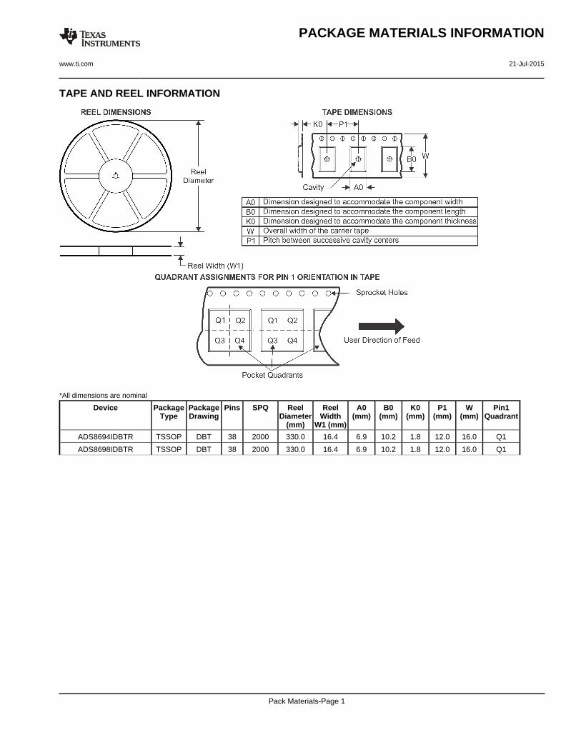
TAPE AND REEL INFORMATION
*All dimensions are nominal
Device PackageType
PackageDrawing
Pins SPQ ReelDiameter
(mm)
ReelWidth
W1 (mm)
A0(mm)
B0(mm)
K0(mm)
P1(mm)
W(mm)
Pin1Quadrant
ADS8694IDBTR TSSOP DBT 38 2000 330.0 16.4 6.9 10.2 1.8 12.0 16.0 Q1
ADS8698IDBTR TSSOP DBT 38 2000 330.0 16.4 6.9 10.2 1.8 12.0 16.0 Q1
PACKAGE MATERIALS INFORMATION
www.ti.com 21-Jul-2015
Pack Materials-Page 1

*All dimensions are nominal
Device Package Type Package Drawing Pins SPQ Length (mm) Width (mm) Height (mm)
ADS8694IDBTR TSSOP DBT 38 2000 367.0 367.0 38.0
ADS8698IDBTR TSSOP DBT 38 2000 367.0 367.0 38.0
PACKAGE MATERIALS INFORMATION
www.ti.com 21-Jul-2015
Pack Materials-Page 2
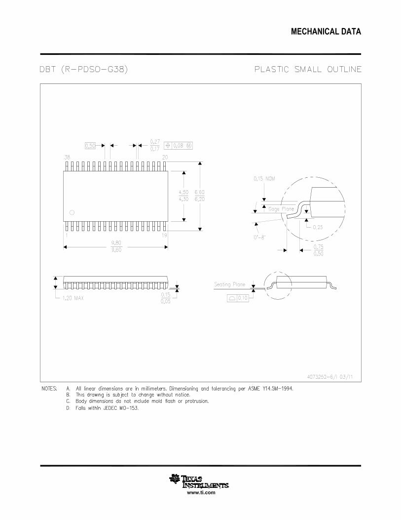
IMPORTANT NOTICE
Texas Instruments Incorporated and its subsidiaries (TI) reserve the right to make corrections, enhancements, improvements and otherchanges to its semiconductor products and services per JESD46, latest issue, and to discontinue any product or service per JESD48, latestissue. Buyers should obtain the latest relevant information before placing orders and should verify that such information is current andcomplete. All semiconductor products (also referred to herein as “components”) are sold subject to TI’s terms and conditions of salesupplied at the time of order acknowledgment.TI warrants performance of its components to the specifications applicable at the time of sale, in accordance with the warranty in TI’s termsand conditions of sale of semiconductor products. Testing and other quality control techniques are used to the extent TI deems necessaryto support this warranty. Except where mandated by applicable law, testing of all parameters of each component is not necessarilyperformed.TI assumes no liability for applications assistance or the design of Buyers’ products. Buyers are responsible for their products andapplications using TI components. To minimize the risks associated with Buyers’ products and applications, Buyers should provideadequate design and operating safeguards.TI does not warrant or represent that any license, either express or implied, is granted under any patent right, copyright, mask work right, orother intellectual property right relating to any combination, machine, or process in which TI components or services are used. Informationpublished by TI regarding third-party products or services does not constitute a license to use such products or services or a warranty orendorsement thereof. Use of such information may require a license from a third party under the patents or other intellectual property of thethird party, or a license from TI under the patents or other intellectual property of TI.Reproduction of significant portions of TI information in TI data books or data sheets is permissible only if reproduction is without alterationand is accompanied by all associated warranties, conditions, limitations, and notices. TI is not responsible or liable for such altereddocumentation. Information of third parties may be subject to additional restrictions.Resale of TI components or services with statements different from or beyond the parameters stated by TI for that component or servicevoids all express and any implied warranties for the associated TI component or service and is an unfair and deceptive business practice.TI is not responsible or liable for any such statements.Buyer acknowledges and agrees that it is solely responsible for compliance with all legal, regulatory and safety-related requirementsconcerning its products, and any use of TI components in its applications, notwithstanding any applications-related information or supportthat may be provided by TI. Buyer represents and agrees that it has all the necessary expertise to create and implement safeguards whichanticipate dangerous consequences of failures, monitor failures and their consequences, lessen the likelihood of failures that might causeharm and take appropriate remedial actions. Buyer will fully indemnify TI and its representatives against any damages arising out of the useof any TI components in safety-critical applications.In some cases, TI components may be promoted specifically to facilitate safety-related applications. With such components, TI’s goal is tohelp enable customers to design and create their own end-product solutions that meet applicable functional safety standards andrequirements. Nonetheless, such components are subject to these terms.No TI components are authorized for use in FDA Class III (or similar life-critical medical equipment) unless authorized officers of the partieshave executed a special agreement specifically governing such use.Only those TI components which TI has specifically designated as military grade or “enhanced plastic” are designed and intended for use inmilitary/aerospace applications or environments. Buyer acknowledges and agrees that any military or aerospace use of TI componentswhich have not been so designated is solely at the Buyer's risk, and that Buyer is solely responsible for compliance with all legal andregulatory requirements in connection with such use.TI has specifically designated certain components as meeting ISO/TS16949 requirements, mainly for automotive use. In any case of use ofnon-designated products, TI will not be responsible for any failure to meet ISO/TS16949.
Products ApplicationsAudio www.ti.com/audio Automotive and Transportation www.ti.com/automotiveAmplifiers amplifier.ti.com Communications and Telecom www.ti.com/communicationsData Converters dataconverter.ti.com Computers and Peripherals www.ti.com/computersDLP® Products www.dlp.com Consumer Electronics www.ti.com/consumer-appsDSP dsp.ti.com Energy and Lighting www.ti.com/energyClocks and Timers www.ti.com/clocks Industrial www.ti.com/industrialInterface interface.ti.com Medical www.ti.com/medicalLogic logic.ti.com Security www.ti.com/securityPower Mgmt power.ti.com Space, Avionics and Defense www.ti.com/space-avionics-defenseMicrocontrollers microcontroller.ti.com Video and Imaging www.ti.com/videoRFID www.ti-rfid.comOMAP Applications Processors www.ti.com/omap TI E2E Community e2e.ti.comWireless Connectivity www.ti.com/wirelessconnectivity
Mailing Address: Texas Instruments, Post Office Box 655303, Dallas, Texas 75265Copyright © 2016, Texas Instruments Incorporated