Embed Size (px)
Citation preview
1.8-2.7 GHz 2W High Linearity 5V 2-Stage Power Amplifier
BMT333
1
Rev. D
BeRex website: www.berex.com email: [email protected]
Specifications and information are subject to change and products may be discontinued without notice. BeRex is a trademark of BeRex.
All other trademarks are the property of their respective owners. © 2018 BeRex
• +5V/550mA at operating bias condition • Gain = 25.5 dB @ 2.65 GHz • P1dB = 33.5 dBm @ 2.65GHz • LTE 10M ACLR = 22.7dBm Output Power at -50dBc @ 2.65GHz • Intergrated interstage matching • Lead-free/Green/RoHS-compliant QFN5x5 SMT package
The BMT333 is a high dynamic range two-stage power amplifier housed in a lead-free/green/RoHS compliant 5x5mm QFN pack-age. The BMT333 uses a high reliabil-ity InGaP/GaAs HBT process technology. The BMT333 is designed for use where high linearity and gain are required. The BMT333 is able to deliver over 22 dBm output power from 1.8 to 2.7GHz while maintaining supe-rior ACLR performance with a few external matching components. All devices are 100% RF/DC screened.
Product Description
Device Features
1 Device performance _ measured on a BeRex evaluation board at 25°C, 50 Ω 2 OIP3 _ measured on two tones with a output power 23dBm/ tone , F2—F1 = 1 MHz..
Typical Performance1
Parameter Frequency Unit
1.8 2.35 2.55 2.65 GHz
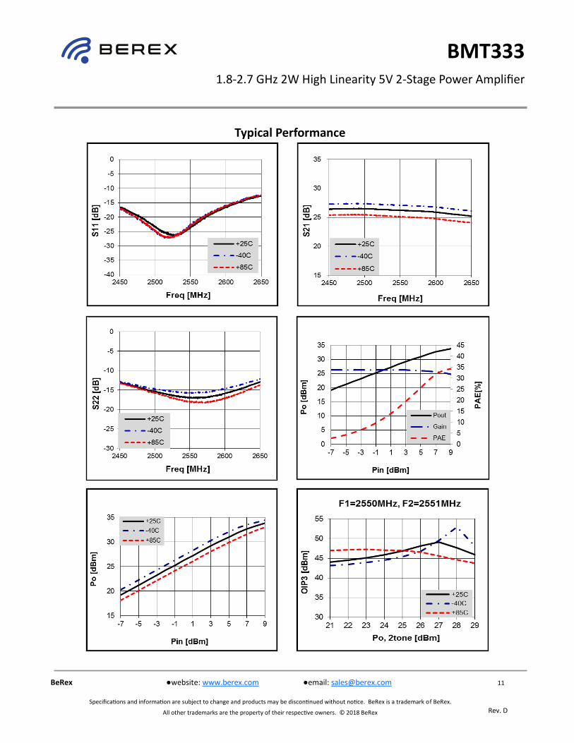
Gain 29.7 27.4 26.2 25.5 dB
S11 -23.4 -25.8 -23.1 -19.3 dB
S22 -12.4 -19.8 -17.0 -18.7 dB
OIP32 45.1 50 48.3 48.2 dBm
P1dB 32.9 34.1 33.3 33.5 dBm
LTE 10M ACLR 22.0 23.5 23.0 22.7 dBm
WCDMA ACLR 22.9 24.4 23.9 23.7 dBm
Noise Figure 5.9 5.3 5.0 5.1 dB
Min. Typical Max. Unit
Bandwidth 1.8 2.7 GHz
Ibias @ (IREF1&2 + IB1&2) 27 mA
IC @ (IC1 + IC2) 550 mA
VCC/Vbias 5.0 V
RTH 8.7 °C/W
Application Circuits
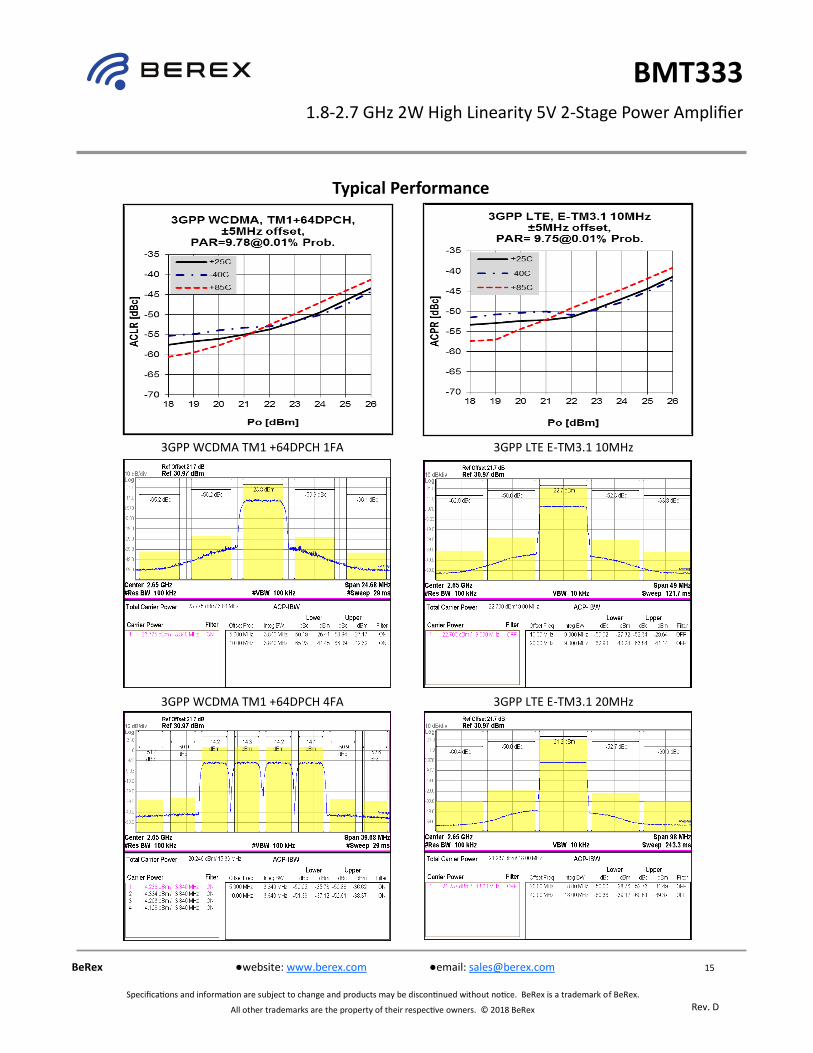
*ACLR Channel Power measured at -50dBc.
- LTE set-up: 3GPP LTE, FDD E-TM3.1, 10MHz BW, ±5MHz offset, PAR 9.75 @0.01% Prob.
- WCDMA set-up: 3GPP WCDMA, TM1+64DPCH, +5MHz offset, PAR 9.78 at 0.01% Prob.
• Base station/Repeaters Infrastructure/Small Cell
• Commercial/Industrial/Military wireless system
• LTE / WCDMA /CDMA Wireless Infrastructure
Applications
Absolute Maximum Ratings
Parameter Unit Rating
Operating Case Temperature °C -40 to +85
Storage Temperature °C -55 to +155
Junction Temperature °C +200
Operating Voltage V +6
Supply Current A 2
Input RF Power dBm 20
1.8-2.7 GHz 2W High Linearity 5V 2-Stage Power Amplifier
BMT333
2
Rev. D
BeRex website: www.berex.com email: [email protected]
Specifications and information are subject to change and products may be discontinued without notice. BeRex is a trademark of BeRex.
All other trademarks are the property of their respective owners. © 2018 BeRex
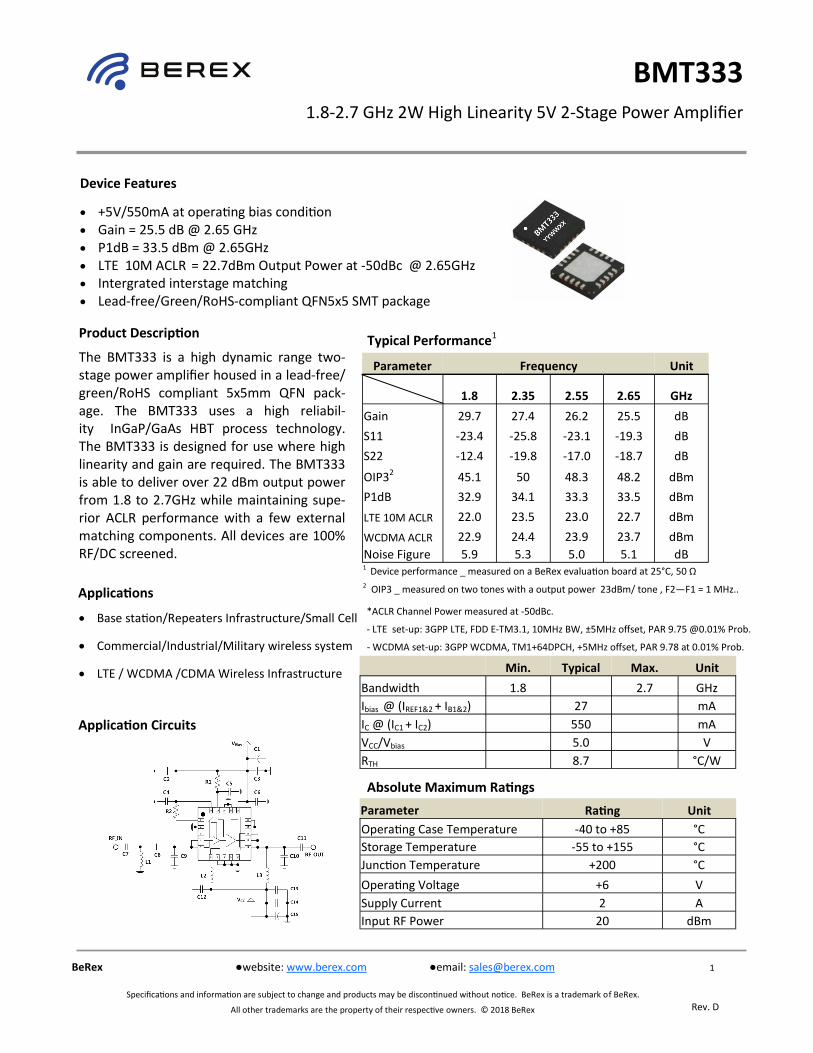
V-I Characteristics BeRex Evaluation Board
Pin Configuration
Pin No. Label
1 IREF1
4,5 RF IN
6 VCC1
11,12,13 RF OUT/VCC2
16 VB2
19 IREF2
20 VB1
2,3,7,8,9,10,14,
15,17,18 GND
Backside Paddle GND
Figure about the reference position of components
1.8-2.7 GHz 2W High Linearity 5V 2-Stage Power Amplifier
BMT333
3
Rev. D
BeRex website: www.berex.com email: [email protected]
Specifications and information are subject to change and products may be discontinued without notice. BeRex is a trademark of BeRex.
All other trademarks are the property of their respective owners. © 2018 BeRex
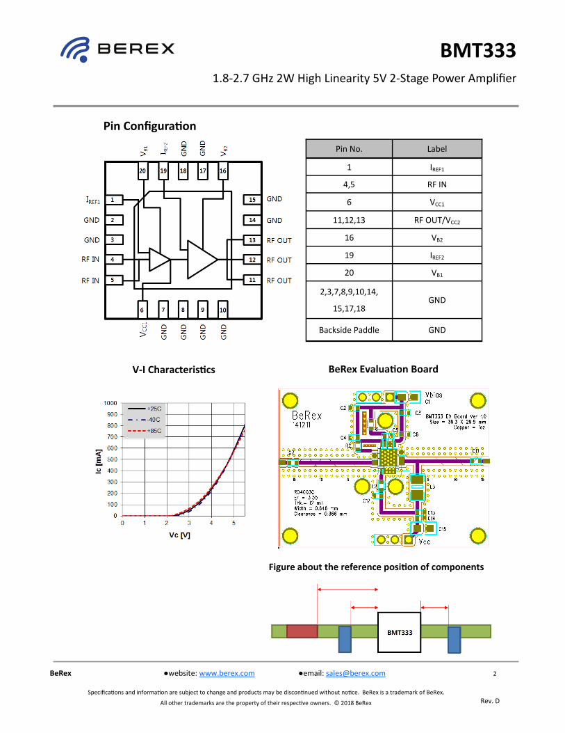
Typical Device Data
S-parameters (Vcc & VBias = +5V, Icq=550mA, Ta=25°C)
Freq S11 S11 S21 S21 S12 S12 S22 S22
[GHz] [Mag] [Ang] [Mag] [Ang] [Mag] [Ang] [Mag] [Ang]
1.8 0.823 48.909 8.999 -14.544 0.002 -47.886 0.851 56.153
1.9 0.829 39.208 8.410 -31.779 0.003 -54.191 0.851 47.807
2.0 0.829 29.005 7.873 -48.880 0.002 -46.186 0.855 39.252
2.1 0.837 19.120 7.499 -65.053 0.001 -44.098 0.846 30.329
2.2 0.840 9.645 7.353 -81.298 0.002 -103.445 0.846 21.294
2.3 0.839 0.350 7.422 -101.020 0.004 -80.766 0.843 12.643
2.4 0.834 -8.866 7.175 -122.701 0.003 -106.587 0.839 3.550
2.5 0.834 -17.528 6.794 -143.783 0.003 -39.239 0.838 -5.571
2.6 0.834 -26.175 6.401 -164.426 0.002 -150.204 0.833 -15.217
2.7 0.833 -34.246 5.948 174.823 0.002 -71.305 0.832 -25.071
S-Parameter
(Vcc & VBias = +5V, Icq = 550mA, Ta= 25 °C, calibrated to device leads)
1.8-2.7 GHz 2W High Linearity 5V 2-Stage Power Amplifier
BMT333
4
Rev. D
BeRex website: www.berex.com email: [email protected]
Specifications and information are subject to change and products may be discontinued without notice. BeRex is a trademark of BeRex.
All other trademarks are the property of their respective owners. © 2018 BeRex
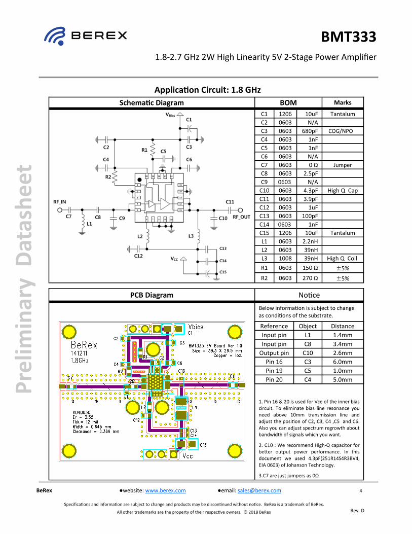
Application Circuit: 1.8 GHz
Schematic Diagram BOM Marks
C1 1206 10uF Tantalum
C2 0603 N/A
C3 0603 680pF COG/NPO
C4 0603 1nF
C5 0603 1nF
C6 0603 N/A
C7 0603 0 Ω Jumper
C8 0603 2.5pF
C9 0603 N/A
C10 0603 4.3pF High Q Cap
C11 0603 3.9pF
C12 0603 1uF
C13 0603 100pF
C14 0603 1nF
C15 1206 10uF Tantalum
L1 0603 2.2nH
L2 0603 39nH
L3 1008 39nH High Q Coil
R1 0603 150 Ω ±5%
R2 0603 270 Ω ±5%
PCB Diagram Notice
Below information is subject to change as conditions of the substrate.
1. Pin 16 & 20 is used for Vce of the inner bias circuit. To eliminate bias line resonance you need above 10mm transmission line and adjust the position of C2, C3, C4 ,C5 and C6. Also you can adjust spectrum regrowth about bandwidth of signals which you want.
2. C10 : We recommend High-Q capacitor for better output power performance. In this document we used 4.3pF(251R14S4R3BV4, EIA 0603) of Johanson Technology.
3.C7 are just jumpers as 0Ω
Pre
limin
ary
Dat
ash
eet
Reference Object Distance
Input pin L1 1.4mm
Input pin C8 3.4mm
Output pin C10 2.6mm
Pin 16 C3 6.0mm
Pin 19 C5 1.0mm
Pin 20 C4 5.0mm
1.8-2.7 GHz 2W High Linearity 5V 2-Stage Power Amplifier
BMT333
5
Rev. D
BeRex website: www.berex.com email: [email protected]
Specifications and information are subject to change and products may be discontinued without notice. BeRex is a trademark of BeRex.
All other trademarks are the property of their respective owners. © 2018 BeRex
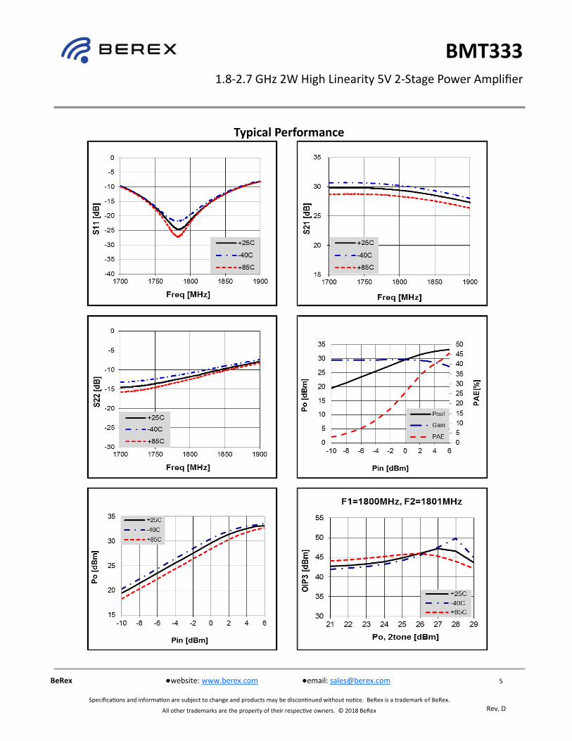
Typical Performance
1.8-2.7 GHz 2W High Linearity 5V 2-Stage Power Amplifier
BMT333
6
Rev. D
BeRex website: www.berex.com email: [email protected]
Specifications and information are subject to change and products may be discontinued without notice. BeRex is a trademark of BeRex.
All other trademarks are the property of their respective owners. © 2018 BeRex
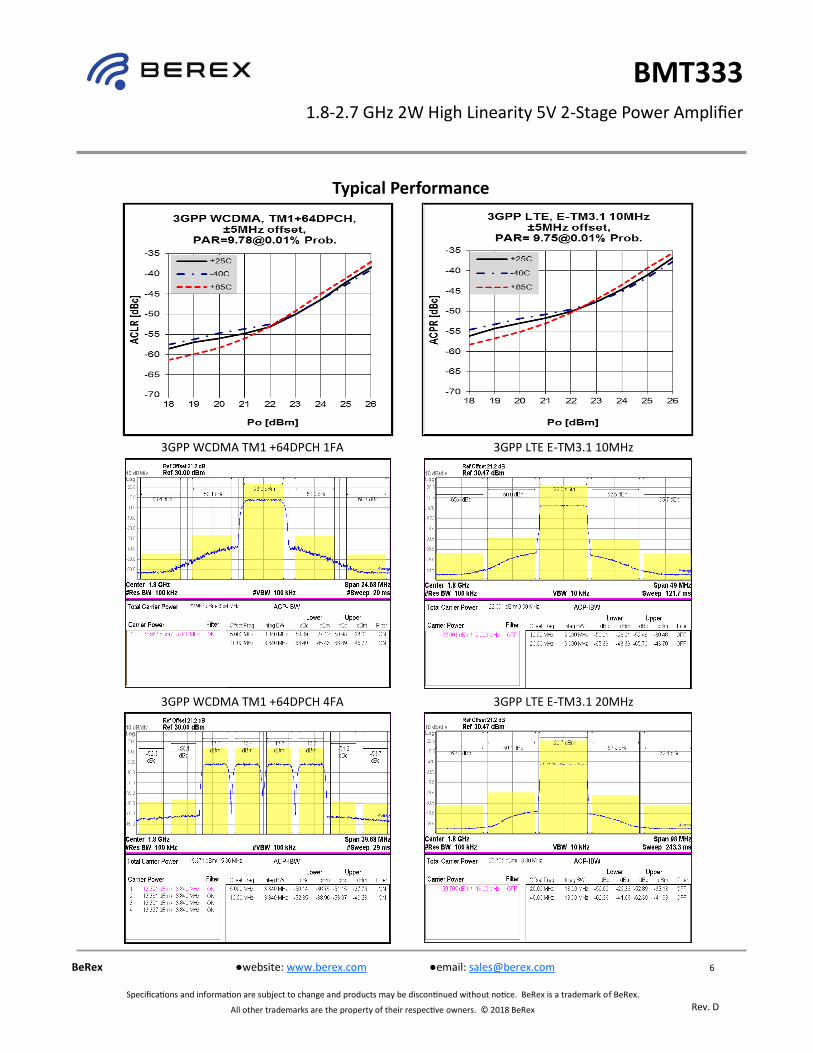
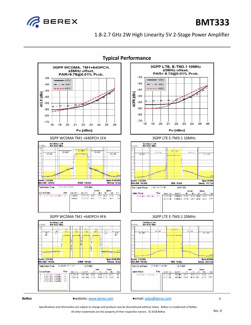
Typical Performance
3GPP WCDMA TM1 +64DPCH 1FA 3GPP LTE E-TM3.1 10MHz
3GPP WCDMA TM1 +64DPCH 4FA 3GPP LTE E-TM3.1 20MHz

1.8-2.7 GHz 2W High Linearity 5V 2-Stage Power Amplifier
BMT333
7
Rev. D
BeRex website: www.berex.com email: [email protected]
Specifications and information are subject to change and products may be discontinued without notice. BeRex is a trademark of BeRex.
All other trademarks are the property of their respective owners. © 2018 BeRex
Application Circuit: 2.35 GHz
1.8-2.7 GHz 2W High Linearity 5V 2-Stage Power Amplifier
BMT333
Schematic Diagram BOM Marks
C1 1206 10uF Tantalum
C2 0603 N/A
C3 0603 680pF COG/NPO
C4 0603 1nF
C5 0603 1nF
C6 0603 27pF COG/NPO
C7 0603 0 Ω Jumper
C8 0603 1.2pF
C9 0603 1.2pF
C10 0603 3.3pF High Q Cap
C11 0603 10pF
C12 0603 1nF
C13 0603 100pF
C14 0603 1nF
C15 1206 10uF Tantalum
L1 0603 N/A
L2 0603 0 Ω Jumper
L3 1008 18nH High Q Coil
R1 0603 150 Ω ±5%
R2 0603 270 Ω ±5%
PCB Diagram Notice
Below information is subject to change as conditions of the substrate.
1. Pin 16 & 20 is used for Vce of the inner bias circuit. To eliminate bias line resonance you need above 10mm transmission line and adjust the position of C2, C3, C4 ,C5 and C6. Also you can adjust spectrum regrowth about bandwidth of signals which you want.
2. C10 : We recommend High-Q capacitor for better output power performance. In this document we used 3.3pF(251R14S3R3BV4, EIA 0603) of Johanson Technology.
3.C7 & L2 are just jumpers as 0Ω
Reference Object Distance
Input pin C8 4.0mm
Input pin C9 3.0mm
Output pin C10 1.2mm
Pin 16 C3 6.2mm
Pin 16 C6 5.0mm
Pin 19 C5 1.0mm
Pin 20 C4 5.0mm
1.8-2.7 GHz 2W High Linearity 5V 2-Stage Power Amplifier
BMT333
8
Rev. D
BeRex website: www.berex.com email: [email protected]
Specifications and information are subject to change and products may be discontinued without notice. BeRex is a trademark of BeRex.
All other trademarks are the property of their respective owners. © 2018 BeRex
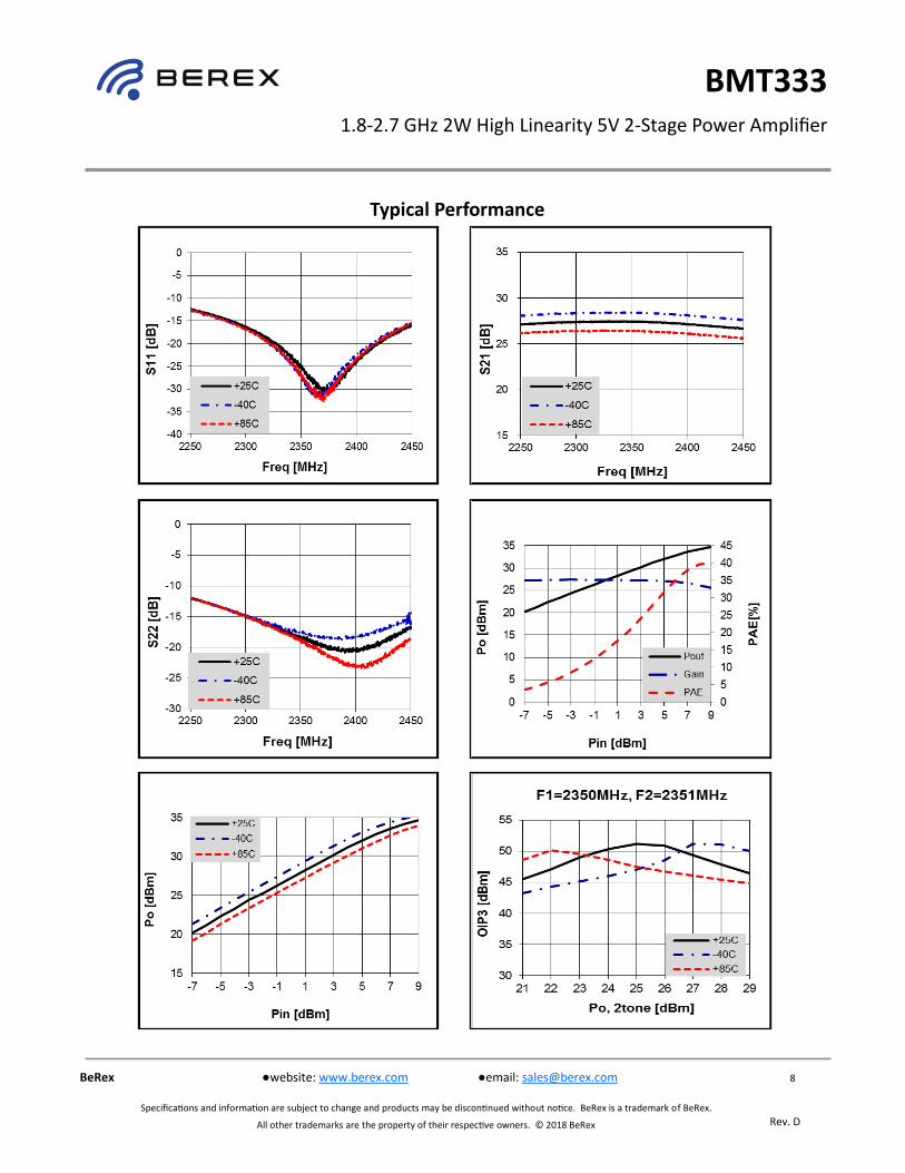
Typical Performance
1.8-2.7 GHz 2W High Linearity 5V 2-Stage Power Amplifier
BMT333
9
Rev. D
BeRex website: www.berex.com email: [email protected]
Specifications and information are subject to change and products may be discontinued without notice. BeRex is a trademark of BeRex.
All other trademarks are the property of their respective owners. © 2018 BeRex
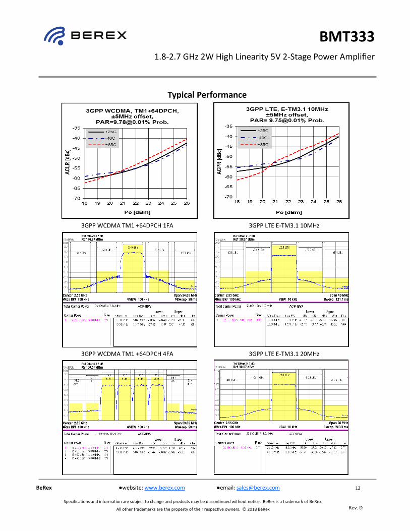
Typical Performance
3GPP WCDMA TM1 +64DPCH 1FA 3GPP LTE E-TM3.1 10MHz
3GPP WCDMA TM1 +64DPCH 4FA 3GPP LTE E-TM3.1 20MHz

1.8-2.7 GHz 2W High Linearity 5V 2-Stage Power Amplifier
BMT333
10
Rev. D
BeRex website: www.berex.com email: [email protected]
Specifications and information are subject to change and products may be discontinued without notice. BeRex is a trademark of BeRex.
All other trademarks are the property of their respective owners. © 2018 BeRex
Application Circuit: 2.55 GHz
Schematic Diagram BOM Marks
C1 1206 10uF Tantalum
C2 0603 1nF
C3 0603 680pF COG/NPO
C4 0603 N/A
C5 0603 1nF
C6 0603 27pF COG/NPO
C7 0603 0 Ω Jumper
C8 0603 1.0pF
C9 0603 1.5pF
C10 0603 3.0pF High Q Cap
C11 0603 10pF
C12 0603 1nF
C13 0603 100pF
C14 0603 1nF
C15 1206 10uF Tantalum
L1 0603 N/A
L2 0603 0 Ω Jumper
L3 1008 18nH High Q Coil
R1 0603 150 Ω ±5%
R2 0603 270 Ω ±5%
PCB Diagram Notice
Below information is subject to change as conditions of the substrate.
1. Pin 16 & 20 is used for Vce of the inner bias circuit. To eliminate bias line resonance you need above 10mm transmission line and adjust the position of C2, C3, C4 ,C5 and C6. Also you can adjust spectrum regrowth about bandwidth of signals which you want.
2. C10 : We recommend High-Q capacitor for better output power performance. In this document we used 3.0pF(251R14S3R0BV4, EIA 0603) of Johanson Technology.
3.C7 & L2 are just jumpers as 0Ω
Reference Object Distance
Input pin C8 4.1mm
Input pin C9 2.2mm
Output pin C10 1.8mm
Pin 16 C3 3.0mm
Pin 16 C6 2.0mm
Pin 19 C5 1.0mm
Pin 20 C4 5.0mm
1.8-2.7 GHz 2W High Linearity 5V 2-Stage Power Amplifier
BMT333
11
Rev. D
BeRex website: www.berex.com email: [email protected]
Specifications and information are subject to change and products may be discontinued without notice. BeRex is a trademark of BeRex.
All other trademarks are the property of their respective owners. © 2018 BeRex
Typical Performance
1.8-2.7 GHz 2W High Linearity 5V 2-Stage Power Amplifier
BMT333
12
Rev. D
BeRex website: www.berex.com email: [email protected]
Specifications and information are subject to change and products may be discontinued without notice. BeRex is a trademark of BeRex.
All other trademarks are the property of their respective owners. © 2018 BeRex
Typical Performance
3GPP WCDMA TM1 +64DPCH 1FA 3GPP LTE E-TM3.1 10MHz
3GPP WCDMA TM1 +64DPCH 4FA 3GPP LTE E-TM3.1 20MHz
1.8-2.7 GHz 2W High Linearity 5V 2-Stage Power Amplifier
BMT333
13
Rev. D
BeRex website: www.berex.com email: [email protected]
Specifications and information are subject to change and products may be discontinued without notice. BeRex is a trademark of BeRex.
All other trademarks are the property of their respective owners. © 2018 BeRex
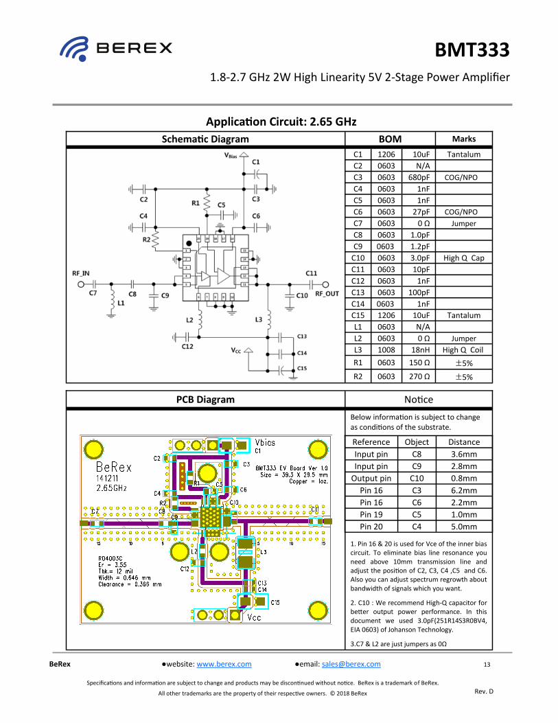
Application Circuit: 2.65 GHz
Schematic Diagram BOM Marks
C1 1206 10uF Tantalum
C2 0603 N/A
C3 0603 680pF COG/NPO
C4 0603 1nF
C5 0603 1nF
C6 0603 27pF COG/NPO
C7 0603 0 Ω Jumper
C8 0603 1.0pF
C9 0603 1.2pF
C10 0603 3.0pF High Q Cap
C11 0603 10pF
C12 0603 1nF
C13 0603 100pF
C14 0603 1nF
C15 1206 10uF Tantalum
L1 0603 N/A
L2 0603 0 Ω Jumper
L3 1008 18nH High Q Coil
R1 0603 150 Ω ±5%
R2 0603 270 Ω ±5%
PCB Diagram Notice
Below information is subject to change as conditions of the substrate.
1. Pin 16 & 20 is used for Vce of the inner bias circuit. To eliminate bias line resonance you need above 10mm transmission line and adjust the position of C2, C3, C4 ,C5 and C6. Also you can adjust spectrum regrowth about bandwidth of signals which you want.
2. C10 : We recommend High-Q capacitor for better output power performance. In this document we used 3.0pF(251R14S3R0BV4, EIA 0603) of Johanson Technology.
3.C7 & L2 are just jumpers as 0Ω
Reference Object Distance
Input pin C8 3.6mm
Input pin C9 2.8mm
Output pin C10 0.8mm
Pin 16 C3 6.2mm
Pin 16 C6 2.2mm
Pin 19 C5 1.0mm
Pin 20 C4 5.0mm

1.8-2.7 GHz 2W High Linearity 5V 2-Stage Power Amplifier
BMT333
14
Rev. D
BeRex website: www.berex.com email: [email protected]
Specifications and information are subject to change and products may be discontinued without notice. BeRex is a trademark of BeRex.
All other trademarks are the property of their respective owners. © 2018 BeRex
Typical Performance
1.8-2.7 GHz 2W High Linearity 5V 2-Stage Power Amplifier
BMT333
15
Rev. D
BeRex website: www.berex.com email: [email protected]
Specifications and information are subject to change and products may be discontinued without notice. BeRex is a trademark of BeRex.
All other trademarks are the property of their respective owners. © 2018 BeRex
Typical Performance
3GPP WCDMA TM1 +64DPCH 1FA 3GPP LTE E-TM3.1 10MHz
3GPP WCDMA TM1 +64DPCH 4FA 3GPP LTE E-TM3.1 20MHz
1.8-2.7 GHz 2W High Linearity 5V 2-Stage Power Amplifier
BMT333
16
Rev. D
BeRex website: www.berex.com email: [email protected]
Specifications and information are subject to change and products may be discontinued without notice. BeRex is a trademark of BeRex.
All other trademarks are the property of their respective owners. © 2018 BeRex
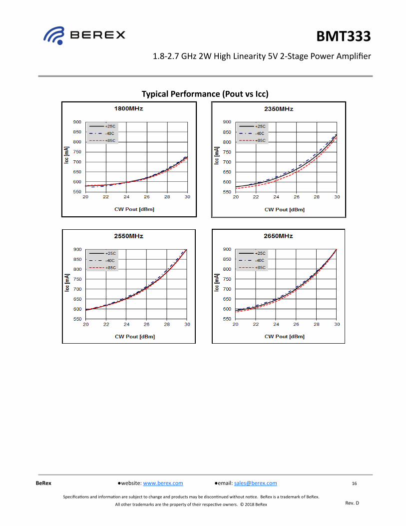
Typical Performance (Pout vs Icc)
1.8-2.7 GHz 2W High Linearity 5V 2-Stage Power Amplifier
BMT333
17
Rev. D
BeRex website: www.berex.com email: [email protected]
Specifications and information are subject to change and products may be discontinued without notice. BeRex is a trademark of BeRex.
All other trademarks are the property of their respective owners. © 2018 BeRex
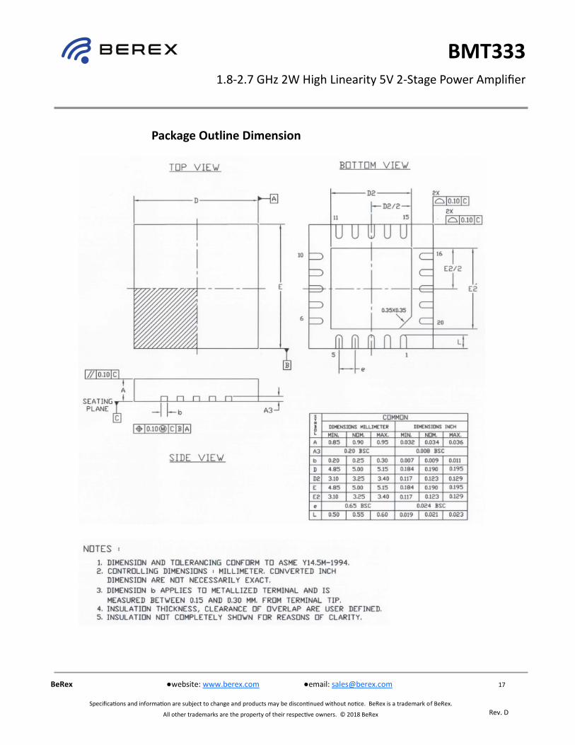
Package Outline Dimension
1.8-2.7 GHz 2W High Linearity 5V 2-Stage Power Amplifier
BMT333
18
Rev. D
BeRex website: www.berex.com email: [email protected]
Specifications and information are subject to change and products may be discontinued without notice. BeRex is a trademark of BeRex.
All other trademarks are the property of their respective owners. © 2018 BeRex
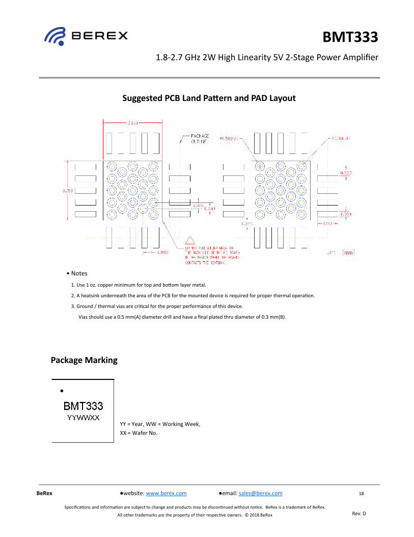
Suggested PCB Land Pattern and PAD Layout
• Notes
1. Use 1 oz. copper minimum for top and bottom layer metal.
2. A heatsink underneath the area of the PCB for the mounted device is required for proper thermal operation.
3. Ground / thermal vias are critical for the proper performance of this device.
Vias should use a 0.5 mm(A) diameter drill and have a final plated thru diameter of 0.3 mm(B).
Package Marking
YY = Year, WW = Working Week,
XX = Wafer No.
1.8-2.7 GHz 2W High Linearity 5V 2-Stage Power Amplifier
BMT333
19
Rev. D
BeRex website: www.berex.com email: [email protected]
Specifications and information are subject to change and products may be discontinued without notice. BeRex is a trademark of BeRex.
All other trademarks are the property of their respective owners. © 2018 BeRex
Lead plating finish
100% Tin Matte finish
(All BeRex products undergoes a 1 hour, 150 degree C, Anneal bake to eliminate thin whisker growth concerns.)
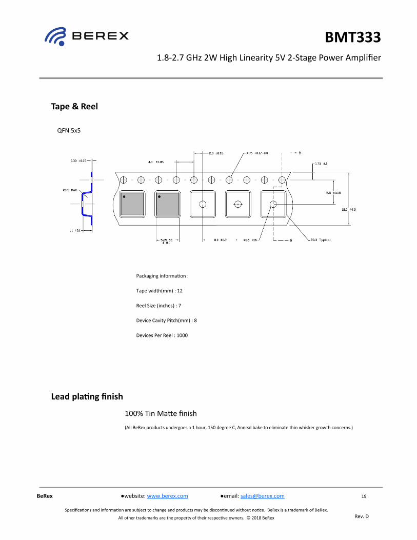
Tape & Reel
Packaging information :
Tape width(mm) : 12
Reel Size (inches) : 7
Device Cavity Pitch(mm) : 8
Devices Per Reel : 1000
QFN 5x5
1.8-2.7 GHz 2W High Linearity 5V 2-Stage Power Amplifier
BMT333
20
Rev. D
BeRex website: www.berex.com email: [email protected]
Specifications and information are subject to change and products may be discontinued without notice. BeRex is a trademark of BeRex.
All other trademarks are the property of their respective owners. © 2018 BeRex
MSL / ESD Rating
ESD Rating:
Value:
Test:
Standard:
ESD Rating:
Value:
Test:
Standard:
MSL Rating:
Standard:
Class 1C
Passes ≥ 1000V to < 2000 V
Human Body Model (HBM)
JEDEC Standard JESD22-A114B
Class C3
Passes >1000V
Charged Device Model (CDM)
JEDEC Standard JESD22-C101F
Level 1 at +260°C convection reflow
JEDEC Standard J-STD-020
NATO CAGE code:
2 N 9 6 F
Pre
limin
ary
Dat
ash
eet


![API 2W [1993]](https://img.pdfslide.us/doc/110x75/577cd4db1a28ab9e78994d52/api-2w-1993.jpg)