Embed Size (px)
Citation preview
HAL Id: hal-02377367https://hal.archives-ouvertes.fr/hal-02377367
Submitted on 23 Nov 2020
HAL is a multi-disciplinary open accessarchive for the deposit and dissemination of sci-entific research documents, whether they are pub-lished or not. The documents may come fromteaching and research institutions in France orabroad, or from public or private research centers.
L’archive ouverte pluridisciplinaire HAL, estdestinée au dépôt et à la diffusion de documentsscientifiques de niveau recherche, publiés ou non,émanant des établissements d’enseignement et derecherche français ou étrangers, des laboratoirespublics ou privés.
175V, > 5.4 MV/cm, 50 m(omega).cm2 at 250°CDiamond MOSFET and its reverse conduction
Cédric Masante, Julien Pernot, Juliette Letellier, David Eon, Nicolas Rouger
To cite this version:Cédric Masante, Julien Pernot, Juliette Letellier, David Eon, Nicolas Rouger. 175V, > 5.4 MV/cm,50 m(omega).cm2 at 250°C Diamond MOSFET and its reverse conduction. 2019 31st InternationalSymposium on Power Semiconductor Devices and ICs (ISPSD), May 2019, Shanghai, China. pp.151-154, �10.1109/ISPSD.2019.8757645�. �hal-02377367�
Author Version. Paper published in the proceedings of IEEE ISPSD 2019 – available at
https://doi.org/10.1109/ISPSD.2019.8757645
175V, > 5.4 MV/cm, 50 mΩ.cm² at 250°C Diamond
MOSFET and its reverse conduction
Cédric Masante, Julien Pernot, Juliette Letellier and David Eon
Inst. NEEL
Univ. Grenoble Alpes, CNRS
Grenoble, France [email protected]
Nicolas Rouger
LAPLACE
Univ. de Toulouse, CNRS
Toulouse, France
Abstract—A diamond MOSFET has been fabricated and
characterized up to 250°C. The fabrication process has been
improved in order to significantly reduce the specific on
resistance, down to 50 mΩ.cm², and the gate leakage current at
high temperature. The maximum electrical field in diamond, at
the breakdown value of 175V, is estimated to be higher than
5.4 MV/cm, with a boron doping of 2×1017 cm-3.
Keywords—Diamond, wide band gap, MOSFET,
D3MOSFET, deep depletion.
I. INTRODUCTION
The use of wide band gap materials to design high blocking voltage and high current density devices is growing in interest. Amongst them, diamond is characterized by its high breakdown field (estimated between 5 and 15 MV/cm), its high carrier mobility (2000 cm/(V.s) for holes) and its exceptional thermal conductivity (22 W/cm.K at room temperature). These properties are crucial for the development of new power devices, which is expected to be a fast growing market in future years. Some diamond power devices have been previously demonstrated experimentally, such as the 2D hole gas MOSFET [1, 2], JFET [3] and MESFET [4], with blocking voltages in the order of 1kV to 2kV. However, even if their performances are very promising, these devices are not reaching yet the full capability of diamond, only demonstrating critical electric field of around 2MV/cm in diamond.
Complementary to these existing architectures, we proposed the use of the deep depletion concept to design a MOSFET relying on bulk conduction, taking advantage of the full potentialities of diamond. Such concept has been demonstrated in previous studies [5, 6] thanks to the recent efforts to control the diamond/Al2O3 interface [7]. However, improvements had to be done to reach the on state diamond potentialities. The devices fabricated in [5, 6] are exhibiting very large contact resistances. This work presents results obtained with an improved fabrication process.
II. DEEP DEPLETION CONCEPT FOR DIAMOND MOSFET
The working principle of this device is extensively discussed in [8]. It relies on the capability of wide band gap semiconductors to have a very stable depletion regime even for high gate biases, past the inversion threshold (so called deep depletion), and high temperatures. Thanks to such a stable deep depletion regime, it becomes possible to deplete
This work is funded by the French ministry of research and French ANR research agency under grants: ANR-16-CE05-0023, #Diamond-
HVDC
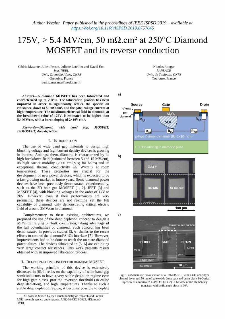
a)
HPHT insulating Ib Diamond plate
p-type Diamond channel [B]=2×1017 cm-3
Ti/Pt/Au
Source DrainGate
p++diamond
RC,S RC,D
RGS RCh RGD
SCR
Al2O3
b)
c)
10 µmSubstrate
p-type layer
p++
Metal
SOURCE DRAINGATE
Drain Source surface
Metal
p++
Fig. 1. a) Schematic cross section of a D3MOSFET, with a 430 nm p-type channel layer and 50 nm of gate oxide (zero gate and drain bias). b) Optical
top view of a fabricated D3MOSFETs. c) SEM view of the elementary
transistor with a tilt angle close to 90°.
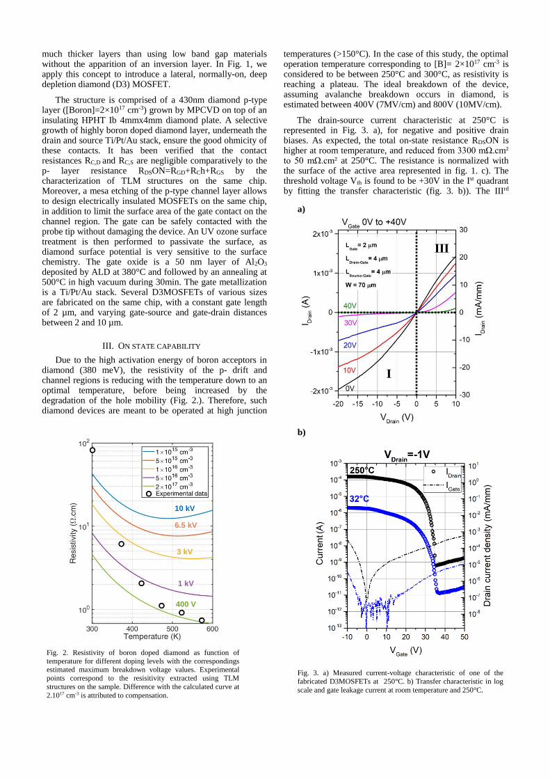
much thicker layers than using low band gap materials without the apparition of an inversion layer. In Fig. 1, we apply this concept to introduce a lateral, normally-on, deep depletion diamond (D3) MOSFET.
The structure is comprised of a 430nm diamond p-type layer ([Boron]=2×1017 cm-3) grown by MPCVD on top of an insulating HPHT Ib 4mmx4mm diamond plate. A selective growth of highly boron doped diamond layer, underneath the drain and source Ti/Pt/Au stack, ensure the good ohmicity of these contacts. It has been verified that the contact resistances RC,D and RC,S are negligible comparatively to the p- layer resistance RDSON=RGD+RCh+RGS by the characterization of TLM structures on the same chip. Moreover, a mesa etching of the p-type channel layer allows to design electrically insulated MOSFETs on the same chip, in addition to limit the surface area of the gate contact on the channel region. The gate can be safely contacted with the probe tip without damaging the device. An UV ozone surface treatment is then performed to passivate the surface, as diamond surface potential is very sensitive to the surface chemistry. The gate oxide is a 50 nm layer of Al2O3 deposited by ALD at 380°C and followed by an annealing at 500°C in high vacuum during 30min. The gate metallization is a Ti/Pt/Au stack. Several D3MOSFETs of various sizes are fabricated on the same chip, with a constant gate length of 2 µm, and varying gate-source and gate-drain distances between 2 and 10 µm.
III. ON STATE CAPABILITY
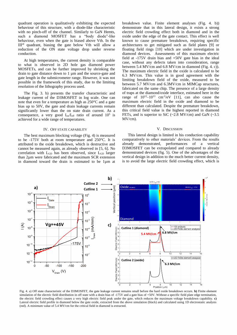
Due to the high activation energy of boron acceptors in diamond (380 meV), the resistivity of the p- drift and channel regions is reducing with the temperature down to an optimal temperature, before being increased by the degradation of the hole mobility (Fig. 2.). Therefore, such diamond devices are meant to be operated at high junction
temperatures (>150°C). In the case of this study, the optimal operation temperature corresponding to [B]= 2×1017 cm-3 is considered to be between 250°C and 300°C, as resistivity is reaching a plateau. The ideal breakdown of the device, assuming avalanche breakdown occurs in diamond, is estimated between 400V (7MV/cm) and 800V (10MV/cm).
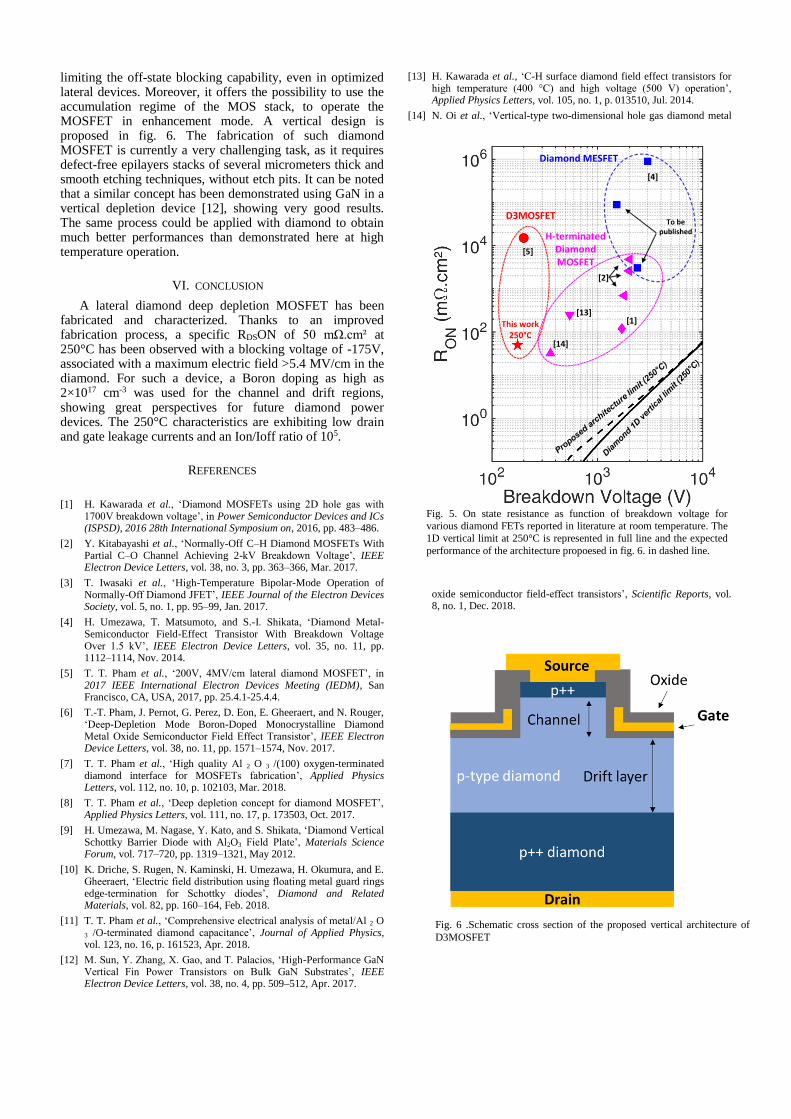
The drain-source current characteristic at 250°C is represented in Fig. 3. a), for negative and positive drain biases. As expected, the total on-state resistance RDSON is higher at room temperature, and reduced from 3300 mΩ.cm² to 50 mΩ.cm² at 250°C. The resistance is normalized with the surface of the active area represented in fig. 1. c). The threshold voltage Vth is found to be +30V in the Ist quadrant by fitting the transfer characteristic (fig. 3. b)). The IIIrd
a)
III
I
b)
Fig. 3. a) Measured current-voltage characteristic of one of the
fabricated D3MOSFETs at 250°C. b) Transfer characteristic in log
scale and gate leakage current at room temperature and 250°C.
10 kV
6.5 kV
3 kV
1 kV
400 V
Fig. 2. Resistivity of boron doped diamond as function of
temperature for different doping levels with the correspondings estimated maximum breakdown voltage values. Experimental
points correspond to the resisitivity extracted using TLM
structures on the sample. Difference with the calculated curve at
2.1017 cm-3 is attributed to compensation.
a)
b)
c)
Cutline 1
Cutline 2
Cutline 1 (diamond)
Cutline 2 (oxide)6.3 MV/cm
5.4 MV/cm 6.8 MV/cm
Fig. 4. a) Off state characteristic of the D3MOSFET, the gate leakage current remains small before the hard oxide breakdown occurs. b) Finite element
simulation of the electric field distribution in off state with a drain bias of -175V and a gate bias of +50V. Without a specific field plate edge termination,
the electric field crowding effect causes a very high electric field peak under the gate, which reduces the maximum voltage breakdown capability. c) Lateral electric field profile in diamond below the gate oxide, extracted from the above simulation (black) and calculated using 1D electrostatic analysis
(red). A minimum value of 5.4 MV/cm for the critical field in diamond is extracted.
quadrant operation is qualitatively exhibiting the expected behaviour of this structure, with a diode-like characteristic with no pinch-off of the channel. Similarly to GaN Hemts, such a diamond MOSFET has a “body diode”-like behaviour, even when the gate is biased above Vth. In the IIIrd quadrant, biasing the gate below Vth will allow a reduction of the ON state voltage drop under reverse conduction.
At high temperatures, the current density is comparable to what is observed in 2D hole gas diamond power MOSFETs, and can be further improved by shrinking the drain to gate distance down to 1 µm and the source-gate and gate length in the submicrometer range. However, it was not possible in the framework of this study, due to the limiting resolution of the lithography process used.
The Fig. 3. b) presents the transfer characteristic and leakage current of the D3MOSFET in log scale. One can note that even for a temperature as high as 250°C and a gate bias up to 50V, the gate and drain leakage currents remain significantly lower than the on state drain current. As a consequence, a very good Ion/Ioff ratio of around 105 is achieved for a wide range of temperatures.
IV. OFF STATE CAPABILITY
The best maximum blocking voltage (Fig. 4) is measured to be -175V both at room temperature and 250°C. It is attributed to the oxide breakdown, which is destructive and cannot be measured again, as already observed in [5, 6]. No correlation with LGD has been observed, since LGD larger than 2µm were fabricated and the maximum SCR extension in diamond toward the drain is estimated to be 1µm at
breakdown value. Finite element analyses (Fig. 4. b)) demonstrate that in this lateral design, it exists a strong electric field crowding effect both in diamond and in the oxide under the edge of the gate contact. This effect is well known to cause premature breakdown, requiring specific architectures to get mitigated such as field plates [9] or floating field rings [10] which are under investigation in diamond devices. Assessments of this maximum electric field at -175V drain bias and +50V gate bias in the ideal case, without any defects taken into consideration, range between 5.4 MV/cm and 6.8 MV/cm in diamond (Fig. 4. c)). The maximum electric field in the oxide is calculated to be 6.3 MV/cm. This value is in good agreement with the limiting breakdown field of the oxide, measured to be between 5.7 MV/cm and 6.3MV/cm in MIMCap structures, fabricated on the same chip. The presence of a large density of traps at the diamond/oxide interface, estimated here in the range of 1012–1013 cm-2/eV [11], can also cause the maximum electric field in the oxide and diamond to be different than calculated. Despite the premature breakdown, this critical field value is the highest reported in diamond FETs, and is superior to SiC (~2.8 MV/cm) and GaN (~3.5 MV/cm).
V. DISCUSSION
This lateral design is limited in his conduction capability comparatively to other materials’ devices. From the results already demonstrated, performances of a vertical D3MOSFET can be extrapolated and compared to already demonstrated devices (fig. 5). One of the advantages of the vertical design in addition to the much better current density, is to avoid the large electric field crowding effect, which is
limiting the off-state blocking capability, even in optimized lateral devices. Moreover, it offers the possibility to use the accumulation regime of the MOS stack, to operate the MOSFET in enhancement mode. A vertical design is proposed in fig. 6. The fabrication of such diamond MOSFET is currently a very challenging task, as it requires defect-free epilayers stacks of several micrometers thick and smooth etching techniques, without etch pits. It can be noted that a similar concept has been demonstrated using GaN in a vertical depletion device [12], showing very good results. The same process could be applied with diamond to obtain much better performances than demonstrated here at high temperature operation.
VI. CONCLUSION
A lateral diamond deep depletion MOSFET has been fabricated and characterized. Thanks to an improved fabrication process, a specific RDSON of 50 mΩ.cm² at 250°C has been observed with a blocking voltage of -175V, associated with a maximum electric field >5.4 MV/cm in the diamond. For such a device, a Boron doping as high as 2×1017 cm-3 was used for the channel and drift regions, showing great perspectives for future diamond power devices. The 250°C characteristics are exhibiting low drain and gate leakage currents and an Ion/Ioff ratio of 105.
REFERENCES
[1] H. Kawarada et al., ‘Diamond MOSFETs using 2D hole gas with
1700V breakdown voltage’, in Power Semiconductor Devices and ICs (ISPSD), 2016 28th International Symposium on, 2016, pp. 483–486.
[2] Y. Kitabayashi et al., ‘Normally-Off C–H Diamond MOSFETs With Partial C–O Channel Achieving 2-kV Breakdown Voltage’, IEEE Electron Device Letters, vol. 38, no. 3, pp. 363–366, Mar. 2017.
[3] T. Iwasaki et al., ‘High-Temperature Bipolar-Mode Operation of Normally-Off Diamond JFET’, IEEE Journal of the Electron Devices Society, vol. 5, no. 1, pp. 95–99, Jan. 2017.
[4] H. Umezawa, T. Matsumoto, and S.-I. Shikata, ‘Diamond Metal-Semiconductor Field-Effect Transistor With Breakdown Voltage Over 1.5 kV’, IEEE Electron Device Letters, vol. 35, no. 11, pp. 1112–1114, Nov. 2014.
[5] T. T. Pham et al., ‘200V, 4MV/cm lateral diamond MOSFET’, in 2017 IEEE International Electron Devices Meeting (IEDM), San Francisco, CA, USA, 2017, pp. 25.4.1-25.4.4.
[6] T.-T. Pham, J. Pernot, G. Perez, D. Eon, E. Gheeraert, and N. Rouger, ‘Deep-Depletion Mode Boron-Doped Monocrystalline Diamond Metal Oxide Semiconductor Field Effect Transistor’, IEEE Electron Device Letters, vol. 38, no. 11, pp. 1571–1574, Nov. 2017.
[7] T. T. Pham et al., ‘High quality Al 2 O 3 /(100) oxygen-terminated diamond interface for MOSFETs fabrication’, Applied Physics Letters, vol. 112, no. 10, p. 102103, Mar. 2018.
[8] T. T. Pham et al., ‘Deep depletion concept for diamond MOSFET’, Applied Physics Letters, vol. 111, no. 17, p. 173503, Oct. 2017.
[9] H. Umezawa, M. Nagase, Y. Kato, and S. Shikata, ‘Diamond Vertical Schottky Barrier Diode with Al2O3 Field Plate’, Materials Science Forum, vol. 717–720, pp. 1319–1321, May 2012.
[10] K. Driche, S. Rugen, N. Kaminski, H. Umezawa, H. Okumura, and E. Gheeraert, ‘Electric field distribution using floating metal guard rings edge-termination for Schottky diodes’, Diamond and Related Materials, vol. 82, pp. 160–164, Feb. 2018.
[11] T. T. Pham et al., ‘Comprehensive electrical analysis of metal/Al 2 O
3 /O-terminated diamond capacitance’, Journal of Applied Physics, vol. 123, no. 16, p. 161523, Apr. 2018.
[12] M. Sun, Y. Zhang, X. Gao, and T. Palacios, ‘High-Performance GaN Vertical Fin Power Transistors on Bulk GaN Substrates’, IEEE Electron Device Letters, vol. 38, no. 4, pp. 509–512, Apr. 2017.
[13] H. Kawarada et al., ‘C-H surface diamond field effect transistors for high temperature (400 °C) and high voltage (500 V) operation’, Applied Physics Letters, vol. 105, no. 1, p. 013510, Jul. 2014.
[14] N. Oi et al., ‘Vertical-type two-dimensional hole gas diamond metal
oxide semiconductor field-effect transistors’, Scientific Reports, vol. 8, no. 1, Dec. 2018.
Diamond MESFET
D3MOSFET
H-terminatedDiamondMOSFET
This work250°C
[5]
[4]
[1]
[2]
[13]
[14]
To bepublished
Fig. 5. On state resistance as function of breakdown voltage for
various diamond FETs reported in literature at room temperature. The
1D vertical limit at 250°C is represented in full line and the expected
performance of the architecture propoesed in fig. 6. in dashed line.
Fig. 6 .Schematic cross section of the proposed vertical architecture of
D3MOSFET