Embed Size (px)
Citation preview

www.l inear.com
July 2012 Volume 22 Number 2
I N T H I S I S S U E
Caption
pushbutton controller 10
15V, 2.5A monolithic buck-
boost with 95% efficiency
and low noise 17
easy 2-supply current
sharing 20
sub-1mm height 24V, 15A
monolithic regulator 26
deliver 25A at 12V from
inputs to 60V 28
Combined Voltage and Current Control Loops Simplify LED Drivers, High Capacity Battery/Supercap Chargers & MPPT* Solar ApplicationsXin (Shin) Qi
The rapid expansion of constant-current/constant-voltage (CC-CV) applications, especially in LED lighting and high capacity battery and supercapacitor chargers challenges power supply designers to keep pace with the increasingly complicated interplay of current and voltage control loops. A switch-mode converter designed specifically
for CC-CV offers a clear advantage, especially when the supply has limited power, or its power is allocated among several competing loads.
Consider, for instance, the challenge of charging a
supercapacitor in a minimum amount of time from
a power-limited supply. To maintain constant input
power, the controlled charging current must decrease
as the output (supercapacitor) voltage increases. The
LT®3796 solves the problem of power limited or con-
stant current/constant voltage regulation by seamlessly
combining a current regulation loop and two volt-
age regulation loops to control an external N-channel
power switch. The inherent wired-OR behavior of its
three transconductance error amplifiers summed into
the compensation pin, VC, ensures that the correct loop
(that is, the one closest to regulation) dominates.
(continued on page 4)
* Maximum Power Point Tracking
The LTC4155 is a monolithic switching battery charger that efficiently delivers 3.5A charge current in a compact PCB footprint. See page 13.

2 | July 2012 : LT Journal of Analog Innovation
In this issue...
Linear in the News
COVER STORY
Combined Voltage and Current Control Loops Simplify LED Drivers, High Capacity Battery/Supercap Chargers & MPPT* Solar ApplicationsXin (Shin) Qi 1
DESIGN FEATURES
Pushbutton On/Off Controller Includes Optional Automatic Turn-On When Handheld Device is Plugged InVui Min Ho 10
I2C-Controlled Li-Ion Power Management IC with Integrated Power Devices Charges High Capacity Batteries from Any 5V Source While Keeping CoolDavid Simmons 13
15V, 2.5A Monolithic Buck-Boost DC/DC Converter with 95% Efficiency and Low Noise OperationEddy Wells 17
Novel Current-Sharing IC Balances Two Supplies with EasePinkesh Sachdev 20
DESIGN IDEAS
What’s New with LTspice IV?Gabino Alonso 24
24V, 15A Step-Down Regulator in Sub-1mm Height Package Pushes Monolithic Performance LimitsStephanie Dai 26
Step-Down Converter Delivers 25A at 12V Output from Inputs Up to 60VVictor Khasiev 28
1.5A Rail-to-Rail Output Synchronous Step-Down Regulator Adjusts with a Single ResistorJeff Zhang 30
back page circuits 32
LINEAR RECEIVES PRESTIGIOUS AWARDS
Over the past several months, Linear Technology received several significant
awards for products, system solutions, and for manufacturing quality and delivery.
Here are the highlights:
Electronic Products 2011 Product of the Year Award: LTC5569 RF Mixer
Electronic Products honored Linear with the selection of the LTC®5569 dual
broadband RF mixer as Product of the Year. From thousands of products,
the editors of Electronic Products selected those they felt are among the
most outstanding. The selection is based on a significant advance in technol-
ogy or its application, innovation in design, or gain in price/performance.
The editors stated, “In order to make LTE, a 4G (fourth-generation) high data-
rate wireless technology attractive to the carrier for deployment, base sta-
tion manufacturers worldwide are trying to build a multiband, multimode
platform that is easily field configured for use in any frequency band and
standard to make the deployment cost attractive. The 26.8dBm IIP3 LTC5569
dual-broadband RF mixer accomplishes this by combining 26.8dBm IIP3,
300mW/ch, and a wide 300MHz to 4GHz frequency range. So a receiver such
as that based on the LTC5569, is capable of working in all of the 700MHz,
880MHz, 1.7GHz, 1.8GHz, 1.9GHz, 2.4GHz, and 2.6GHz bands. In addition,
within each band, the receiver must receive signals that are 60MHz wide,
compared to the previous 20MHz wide without sacrificing performance. The
LTC5569 meets both of these requirements with outstanding performance.”
EN-Genius Network Awards Linear for Products of the Year & the Decade
EN-Genius Network, formerly AnalogZone, selected Linear Technology’s
µModule® family as Best Product of Our Decade. According to the edi-
tor, “The concept of the µModules allows the product designer to
come to the decisions about power management quite late in the
development cycle—simplifying the final product choice.
“Linear has also extended the concept to a family of seventeen ‘System in a
Package’ (SiP) signal chain receiver modules, the first of which, the LTM®9001,
we reviewed here. The SiPs, which feature 12-/14-/16-bit solutions, not
only simplify circuit design for the less than sure RF engineer out there but
they also bypass export regulation control of some individual ADCs.
“All-in-all the µModule concept has been a spectacularly successful commer-
cial and technological story for Linear. We are delighted to congratulate them
on their achievement and to recognize them as the Product of Our Decade.”

July 2012 : LT Journal of Analog Innovation | 3
Linear in the news
EN-Genius Network also selected Linear’s
LTC6946 373MHz to 5.79GHz Integer-N
synthesizer as Product of the Year for
the Best Integer-N Synthesizer. The pub-
lication commented, “The parts are a
welcome addition to Linear’s RF arsenal
and will prove to be equally attractive to
designers who do not have to cope with
large bandwidth issues straight away.”
China Electronics Awards
Several major electronics publications in
China presented Linear with awards:
•EDN China: Innovation Award, Excellent
Product Award for the LTC4000 high
voltage controller and power manager.
•China Electronic Market: Editor’s Choice
Award for the Most Competitive
Power Product: LTC4000
•EEPW Editor’s Choice Awards: Best Analog
Product: LTC6803 battery stack
monitor for hybrid/electric vehicles
Best Amplifier: LT1999 high voltage
bidirectional current sense monitor
•Electronic Products China: Annual
Award: LTM8047/8048 isolated
µModule DC/DC converter
Enics Manufacturing Award
Enics, one of the largest providers of
electronics manufacturing services,
named the best suppliers of the year, and
honored Linear as the Best Component
Manufacturer at the annual Enics Fair in
Zurich, Switzerland.
LINEAR’S STRONG PATENT PORTFOLIO RECOGNIZED
Ocean Tomo announced the leading
companies in patent assets. According
to Ocean Tomo’s ranking, Linear
Technology’s patent portfolio received an
IPQ score of 123—the highest of any major
analog semiconductor company. Ocean
Tomo claims to rate patent assets objec-
tively based on proven statistical method-
ology. This reinforces the value of Linear’s
growing patent portfolio and the com-
pany’s strong analog intellectual property.
CONFERENCES & EVENTS
Power Systems Show 2012, Tokyo Big Sight,
Tokyo, Japan, July 11–13, Booth 6B-301—Linear
will showcase power products, includ-
ing µModule products and FPGA power
management solutions. More info at www.
jma.or.jp/tf/en11/electronics/index.html.
EN-GENIUS NETWORK AWARDS LINEAR FOR PRODUCTS OF THE YEAR & THE DECADEEN-Genius Network, formerly AnalogZone, selected Linear’s µModule products as Best Product of Our Decade. According to the editor, “The concept of the µModules allows the product designer to come to the decisions about power management quite late in the development cycle—simplifying the final product choice.”
4 | July 2012 : LT Journal of Analog Innovation
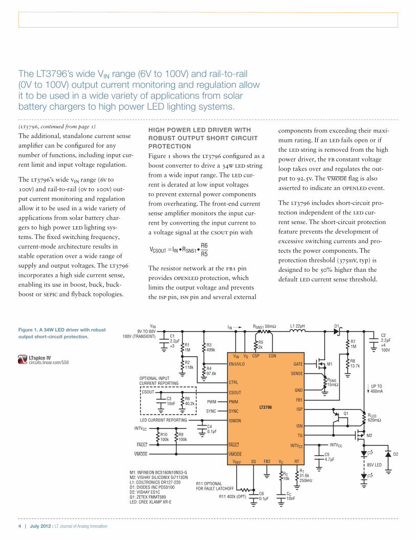
HIGH POWER LED DRIVER WITH ROBUST OUTPUT SHORT CIRCUIT PROTECTION
Figure 1 shows the LT3796 configured as a
boost converter to drive a 34W LED string
from a wide input range. The LED cur-
rent is derated at low input voltages
to prevent external power components
from overheating. The front-end current
sense amplifier monitors the input cur-
rent by converting the input current to
a voltage signal at the CSOUT pin with
V I R RRCSOUT IN SNS= • •1
65
The resistor network at the FB1 pin
provides OPENLED protection, which
limits the output voltage and prevents
the ISP pin, ISN pin and several external
components from exceeding their maxi-
mum rating. If an LED fails open or if
the LED string is removed from the high
power driver, the FB constant voltage
loop takes over and regulates the out-
put to 92.5V. The VMODE flag is also
asserted to indicate an OPENLED event.
The LT3796 includes short-circuit pro-
tection independent of the LED cur-
rent sense. The short-circuit protection
feature prevents the development of
excessive switching currents and pro-
tects the power components. The
protection threshold (375mV, typ) is
designed to be 50% higher than the
default LED current sense threshold.
The additional, standalone current sense
amplifier can be configured for any
number of functions, including input cur-
rent limit and input voltage regulation.
The LT3796’s wide VIN range (6V to
100V) and rail-to-rail (0V to 100V) out-
put current monitoring and regulation
allow it to be used in a wide variety of
applications from solar battery char-
gers to high power LED lighting sys-
tems. The fixed switching frequency,
current-mode architecture results in
stable operation over a wide range of
supply and output voltages. The LT3796
incorporates a high side current sense,
enabling its use in boost, buck, buck-
boost or SEPIC and flyback topologies.
(LT3796, continued from page 1)
The LT3796’s wide VIN range (6V to 100V) and rail-to-rail (0V to 100V) output current monitoring and regulation allow it to be used in a wide variety of applications from solar battery chargers to high power LED lighting systems.
R2118k
CSPVSVIN CSN
SSVREF
R52k
85V LED
LT3796
CTRL
CSOUT
PWM
SYNC
PWM
SYNC
M1: INFINEON BCS160N10NS3-GM2: VISHAY SILICONIX Si7113DNL1: COILTRONICS DR127-220D1: DIODES INC PDS5100D2: VISHAY ES1CQ1: ZETEX FMMT589LED: CREE XLAMP XR-E
ISMON
EN/UVLO
GND
FB1
ISP
ISN
TG
GATE
SENSE
L1 22µHRSNS1 50mΩIIN9V TO 60V
100V (TRANSIENT)
D1
RC10k
RT31.6k250kHz
CC10nF
R3499k
R497.6k
R11M
C12.2µF×3
VIN
C22.2µF×4100V
R813.7k
RSNS15mΩ
RLED620mΩ
M2
Q1
M1
D2
UP TO400mA
R640.2k
C310nF
CSOUT
OPTIONAL INPUTCURRENT REPORTING
R71M
VMODE
FAULT
VMODE
FAULT
LED CURRENT REPORTING
R11 OPTIONALFOR FAULT LATCHOFF
R11 402k (OPT)
VC RTFB2
INTVCC
C54.7µF
C60.1µF
INTVCC
R10100k
R9100k
INTVCCC40.1µF
Figure 1. A 34W LED driver with robust output short-circuit protection.
LTspice IVcircuits.linear.com/558
July 2012 : LT Journal of Analog Innovation | 5
design features
If there is no resistor between the SS pin
and VREF pin, the converter enters hiccup
mode and periodically retries as shown
in the Figure 2. If a resistor is placed
between VREF and SS pin to hold SS pin
higher than 0.2V during LED short, then
the LT3796 enters latchoff mode with
GATE pin low and TG pin high, as shown
in Figure 3. To exit latchoff mode, the
EN/UVLO pin must be toggled low to high.
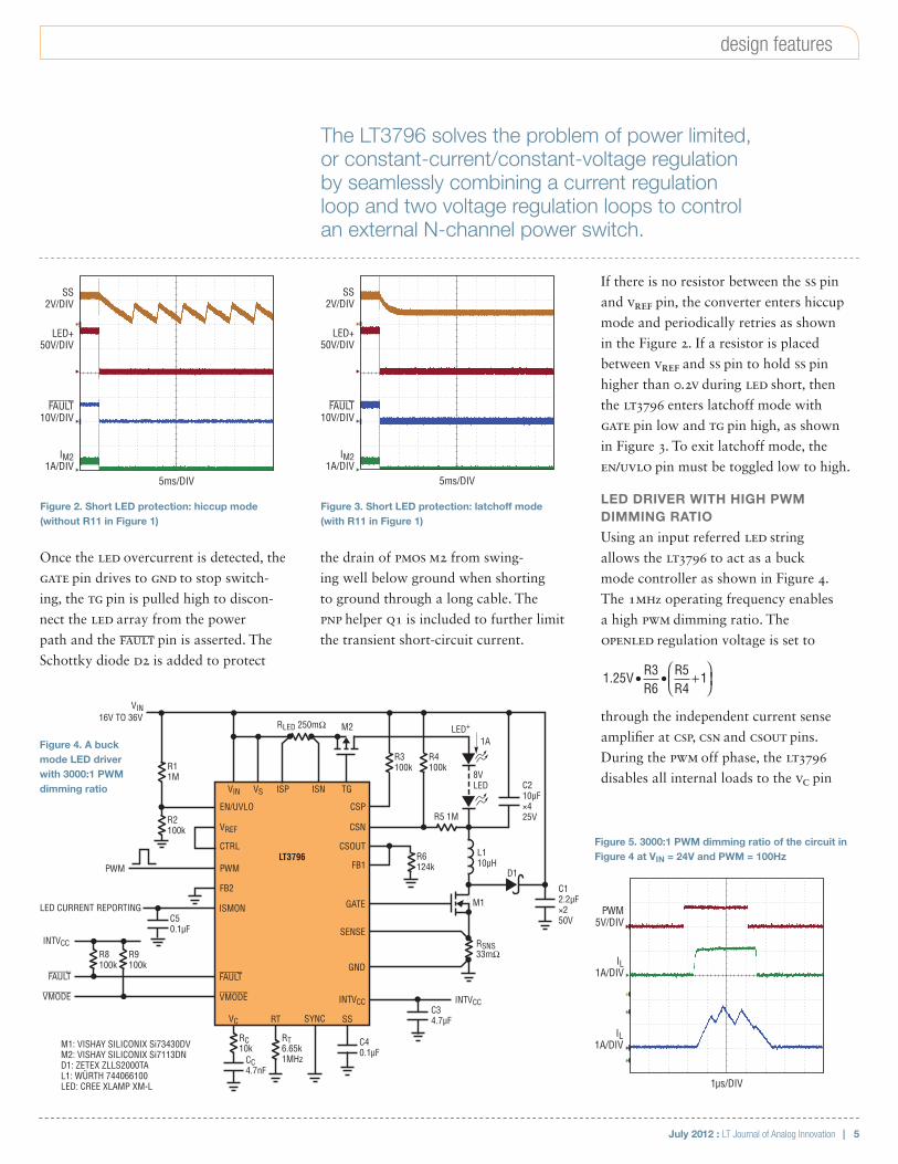
LED DRIVER WITH HIGH PWM DIMMING RATIO
Using an input referred LED string
allows the LT3796 to act as a buck
mode controller as shown in Figure 4.
The 1MHz operating frequency enables
a high PWM dimming ratio. The
OPENLED regulation voltage is set to
1 25 36
54
1. V RR
RR
• • +
through the independent current sense
amplifier at CSP, CSN and CSOUT pins.
During the PWM off phase, the LT3796
disables all internal loads to the VC pin
the drain of PMOS M2 from swing-
ing well below ground when shorting
to ground through a long cable. The
PNP helper Q1 is included to further limit
the transient short-circuit current.
Once the LED overcurrent is detected, the
GATE pin drives to GND to stop switch-
ing, the TG pin is pulled high to discon-
nect the LED array from the power
path and the FAULT pin is asserted. The
Schottky diode D2 is added to protect
The LT3796 solves the problem of power limited, or constant-current/constant-voltage regulation by seamlessly combining a current regulation loop and two voltage regulation loops to control an external N-channel power switch.
5ms/DIV
SS2V/DIV
LED+50V/DIV
FAULT10V/DIV
IM21A/DIV
5ms/DIV
SS2V/DIV
LED+50V/DIV
FAULT10V/DIV
IM21A/DIV
Figure 2. Short LED protection: hiccup mode (without R11 in Figure 1)
Figure 3. Short LED protection: latchoff mode (with R11 in Figure 1)
R2100k
ISPVSVIN TGISN
RT SSVC SYNC
M1
LT3796CTRL
PWM
FB2
ISMON
PWM
LED CURRENT REPORTING
EN/UVLO
VREF
CSOUT
FB1
GATE
SENSE
GND
INTVCC
CSP
CSN
CC4.7nF
R11M
L110µH
RLED 250mΩ M2 LED+16V TO 36V
D1
1A
RT6.65k1MHz
RC10k
C34.7µF
INTVCC
C40.1µF
C50.1µF
VIN
C210µF×425V
R6124k
R3100k
R4100k
R5 1M
RSNS33mΩ
8VLED
C12.2µF×250V
M1: VISHAY SILICONIX Si73430DVM2: VISHAY SILICONIX Si7113DND1: ZETEX ZLLS2000TAL1: WÜRTH 744066100LED: CREE XLAMP XM-L
VMODE
FAULT
VMODE
FAULT
R8100k
R9100k
INTVCC
Figure 4. A buck mode LED driver with 3000:1 PWM dimming ratio
1µs/DIV
PWM5V/DIV
IL1A/DIV
IL1A/DIV
Figure 5. 3000:1 PWM dimming ratio of the circuit in Figure 4 at VIN = 24V and PWM = 100Hz
6 | July 2012 : LT Journal of Analog Innovation
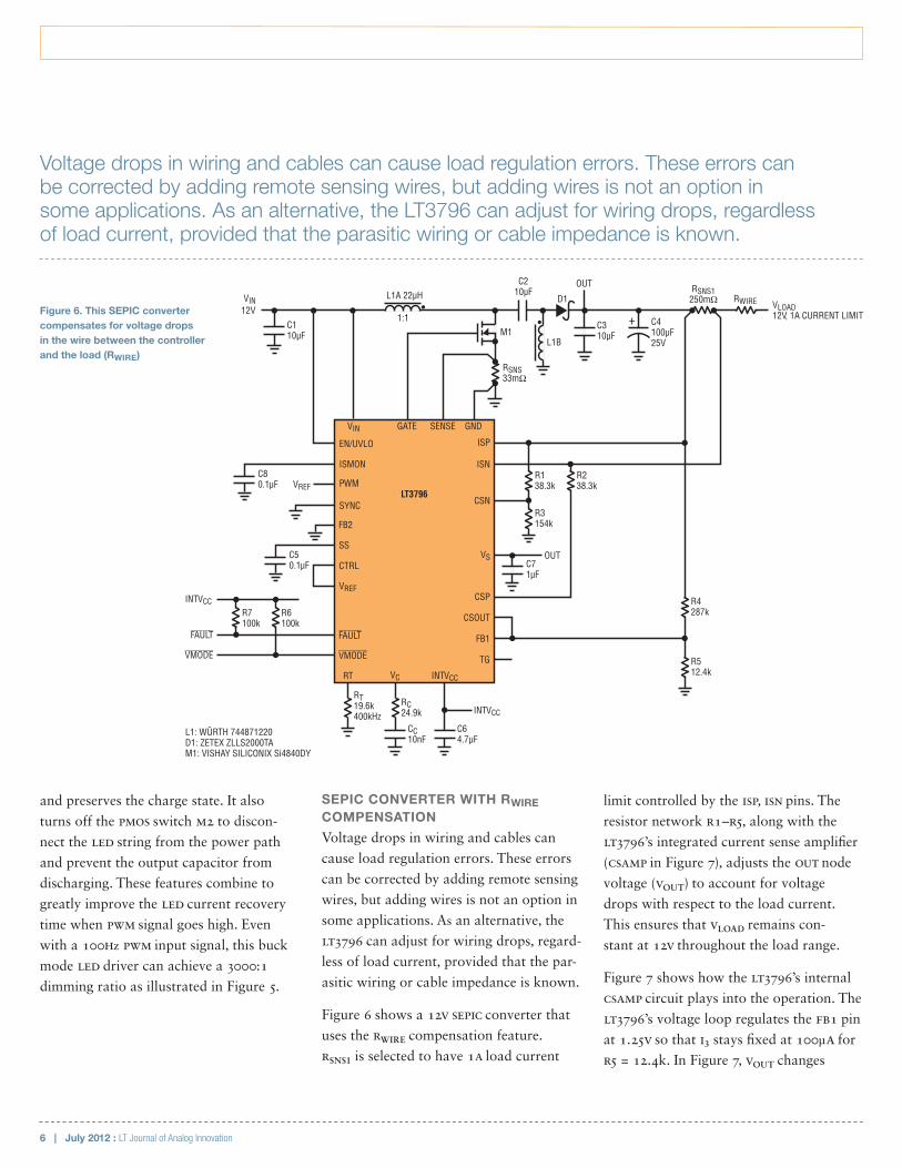
SEPIC CONVERTER WITH RWIRE COMPENSATION
Voltage drops in wiring and cables can
cause load regulation errors. These errors
can be corrected by adding remote sensing
wires, but adding wires is not an option in
some applications. As an alternative, the
LT3796 can adjust for wiring drops, regard-
less of load current, provided that the par-
asitic wiring or cable impedance is known.
Figure 6 shows a 12V SEPIC converter that
uses the RWIRE compensation feature.
RSNS1 is selected to have 1A load current
limit controlled by the ISP, ISN pins. The
resistor network R1–R5, along with the
LT3796’s integrated current sense amplifier
(CSAMP in Figure 7), adjusts the OUT node
voltage (VOUT) to account for voltage
drops with respect to the load current.
This ensures that VLOAD remains con-
stant at 12V throughout the load range.
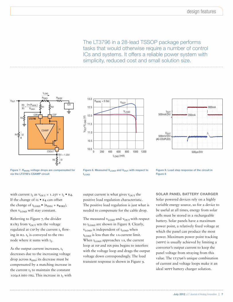
Figure 7 shows how the LT3796’s internal
CSAMP circuit plays into the operation. The
LT3796’s voltage loop regulates the FB1 pin
at 1.25V so that I3 stays fixed at 100µA for
R5 = 12.4k. In Figure 7, VOUT changes
and preserves the charge state. It also
turns off the PMOS switch M2 to discon-
nect the LED string from the power path
and prevent the output capacitor from
discharging. These features combine to
greatly improve the LED current recovery
time when PWM signal goes high. Even
with a 100Hz PWM input signal, this buck
mode LED driver can achieve a 3000:1
dimming ratio as illustrated in Figure 5.
GATE GNDVIN SENSE
RT VC
LT3796PWM
SYNC
FB2
VREF
L1: WÜRTH 744871220D1: ZETEX ZLLS2000TAM1: VISHAY SILICONIX Si4840DY
SS
CTRL
VREF
EN/UVLO
ISMON
CSN
OUTVS
CSP
CSOUT
FB1
TG
INTVCC
INTVCC
ISP
ISN
L1A 22µH
L1BM1
C210µF
OUT
RWIRE VLOAD12V, 1A CURRENT LIMIT
RSNS1250mΩ
12VD1
1:1
CC10nF
RT19.6k400kHz
RC24.9k
C64.7µF
C50.1µF
C80.1µF
C110µF
VIN
C310µF
C4100µF25V
•
RSNS33mΩ
C71µF
•
R138.3k
R238.3k
R3154k
R4287k
R512.4k
+
VMODE
FAULT
VMODE
FAULT
R7100k
R6100k
INTVCC
Figure 6. This SEPIC converter compensates for voltage drops in the wire between the controller and the load (RWIRE)
Voltage drops in wiring and cables can cause load regulation errors. These errors can be corrected by adding remote sensing wires, but adding wires is not an option in some applications. As an alternative, the LT3796 can adjust for wiring drops, regardless of load current, provided that the parasitic wiring or cable impedance is known.
July 2012 : LT Journal of Analog Innovation | 7
design features
with current I2 as VOUT = 1.25V + I2•R4.
If the change of I2•R4 can offset
the change of ILOAD •(RSNS1 + RWIRE),
then VLOAD will stay constant.
Referring to Figure 7, the divider
R1/R3 from VOUT sets the voltage
regulated at CSP by the current I1 flow-
ing in R2. I1 is conveyed to the FB1
node where it sums with I2.
As the output current increases, I1
decreases due to the increasing voltage
drop across RSNS; its decrease must be
compensated by a matching increase in
the current I2 to maintain the constant
100µA into FB2. This increase in I2 with
output current is what gives VOUT the
positive load regulation characteristic.
The positive load regulation is just what is
needed to compensate for the cable drop.
The measured VLOAD and VOUT with respect
to ILOAD are shown in Figure 8. Clearly,
VLOAD is independent of ILOAD when
ILOAD is less than the 1A current limit.
When ILOAD approaches 1A, the current
loop at ISP and ISN pins begins to interfere
with the voltage loop and drags the output
voltage down correspondingly. The load
transient response is shown in Figure 9.
SOLAR PANEL BATTERY CHARGER
Solar powered devices rely on a highly
variable energy source, so for a device to
be useful at all times, energy from solar
cells must be stored in a rechargeable
battery. Solar panels have a maximum
power point, a relatively fixed voltage at
which the panel can produce the most
power. Maximum power point tracking
(MPPT) is usually achieved by limiting a
converter’s output current to keep the
panel voltage from straying from this
value. The LT3796’s unique combination
of current and voltage loops make it an
ideal MPPT battery charger solution.
LT3796
R1
RSNS1
R2
CSP
FB1 = 1.25V
CSN
VOUT
ILOAD
CSOUT
I1
RWIRE
I3
I2
–+
12V
R5
R3
R4
CSAMP
RR
R
RWIRE
SNS
31
2
1=
• ( )
Figure 7. RWIRE voltage drops are compensated for via the LT3796’s CSAMP circuit
ILOAD (mA)
13.0
0 400 600 800 1000 1200200
11.0
10.5
10.0
11.5
12.5
12.0
V OUT
/VLO
AD (V
)
VOUT
VLOAD
RWIRE = 0.5Ω
500µs/DIV
VOUT500mV/DIV
(AC-COUPLED)
IOUT500mA/DIV 200mA
800mA
Figure 8. Measured VLOAD and VOUT with respect to ILOAD
Figure 9. Load step response of the circuit in Figure 6
The LT3796 in a 28-lead TSSOP package performs tasks that would otherwise require a number of control ICs and systems. It offers a reliable power system with simplicity, reduced cost and small solution size.
8 | July 2012 : LT Journal of Analog Innovation
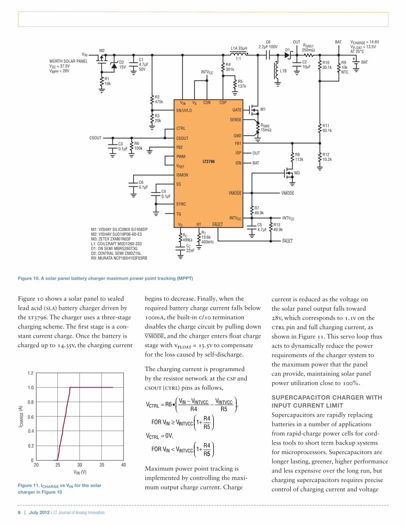
Figure 10 shows a solar panel to sealed
lead acid (SLA) battery charger driven by
the LT3796. The charger uses a three-stage
charging scheme. The first stage is a con-
stant current charge. Once the battery is
charged up to 14.35V, the charging current
current is reduced as the voltage on
the solar panel output falls toward
28V, which corresponds to 1.1V on the
CTRL pin and full charging current, as
shown in Figure 11. This servo loop thus
acts to dynamically reduce the power
requirements of the charger system to
the maximum power that the panel
can provide, maintaining solar panel
power utilization close to 100%.
SUPERCAPACITOR CHARGER WITH INPUT CURRENT LIMIT
Supercapacitors are rapidly replacing
batteries in a number of applications
from rapid-charge power cells for cord-
less tools to short term backup systems
for microprocessors. Supercapacitors are
longer lasting, greener, higher performance
and less expensive over the long run, but
charging supercapacitors requires precise
control of charging current and voltage
begins to decrease. Finally, when the
required battery charge current falls below
100mA, the built-in C/10 termination
disables the charge circuit by pulling down
VMODE, and the charger enters float charge
stage with VFLOAT = 13.5V to compensate
for the loss caused by self-discharge.
The charging current is programmed
by the resistor network at the CSP and
CSOUT (CTRL) pins as follows,
V R V VR
VR
V V
CTRLIN INTVCC INTVCC
IN
= • − −
≥
64 5
,
FOR IINTVCC
CTRL
IN INTVCC
RR
V V
V V RR
1 45
0
1 4
+
=
< +
,
FOR55
Maximum power point tracking is
implemented by controlling the maxi-
mum output charge current. Charge
VIN (V)
1.2
20 30 35 4025
0.4
0.2
0
0.6
0.8
1.0
I CHA
RGE
(A)
Figure 11. ICHARGE vs VIN for the solar charger in Figure 10
Figure 10. A solar panel battery charger maximum power point tracking (MPPT)
CSNVIN VS CSP
RTVC FAULT
LT3796
CTRL
CSOUT
FB2
PWM
TG
M1: VISHAY SILICONIX Si7456DPM2: VISHAY SUD19P06-60-E3M3: ZETEX ZXM61N03FL1: COILCRAFT MSD1260-333D1: ON SEMI MBRS260T3GD2: CENTRAL SEMI CMDZ15LR9: MURATA NCP18XH103F03RB
VREF
ISMON
SYNC
SS
EN/UVLO
FB1
OUTISP
ISN
INTVCC INTVCC
FAULT
GATE
SENSE
GND
L1A 33µHOUT
RSNS1250mΩ
R1030.1k
L1B
WÜRTH SOLAR PANELVOC = 37.5VVMPP = 28V
D1
1:1
RT19.6k400kHz
RC499Ω
CC22nF
C40.1µF
C30.1µF
CSOUT
C14.7µF50V
VIN
BATC210µF
BAT VCHARGE = 14.6VVFLOAT = 13.5VAT 25°C
BAT
R910kNTC
•
R5137k
INTVCC
R4301k
+
R1193.1k
RSNS15mΩ
M1
M3
R1210.2k
R8113k
R320k
R2475k
M2
D215V
R6100k
R110k
C62.2µF 100V
•
C60.1µF
VMODE VMODE
R749.9k
R1349.9k
C54.7µF
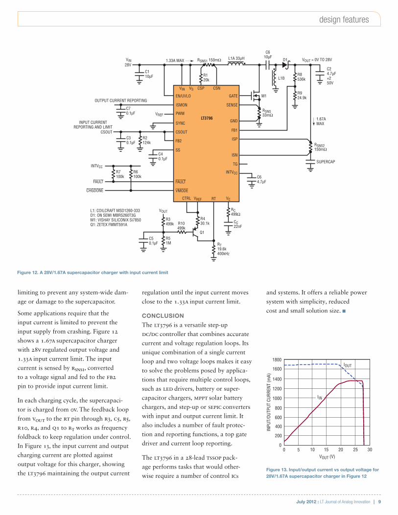
July 2012 : LT Journal of Analog Innovation | 9
design features
limiting to prevent any system-wide dam-
age or damage to the supercapacitor.
Some applications require that the
input current is limited to prevent the
input supply from crashing. Figure 12
shows a 1.67A supercapacitor charger
with 28V regulated output voltage and
1.33A input current limit. The input
current is sensed by RSNS1, converted
to a voltage signal and fed to the FB2
pin to provide input current limit.
In each charging cycle, the supercapaci-
tor is charged from 0V. The feedback loop
from VOUT to the RT pin through R3, C5, R5,
R10, R4, and Q1 to RT works as frequency
foldback to keep regulation under control.
In Figure 13, the input current and output
charging current are plotted against
output voltage for this charger, showing
the LT3796 maintaining the output current
regulation until the input current moves
close to the 1.33A input current limit.
CONCLUSION
The LT3796 is a versatile step-up
DC/DC controller that combines accurate
current and voltage regulation loops. Its
unique combination of a single current
loop and two voltage loops makes it easy
to solve the problems posed by applica-
tions that require multiple control loops,
such as LED drivers, battery or super-
capacitor chargers, MPPT solar battery
chargers, and step-up or SEPIC converters
with input and output current limit. It
also includes a number of fault protec-
tion and reporting functions, a top gate
driver and current loop reporting.
The LT3796 in a 28-lead TSSOP pack-
age performs tasks that would other-
wise require a number of control ICs
and systems. It offers a reliable power
system with simplicity, reduced
cost and small solution size. n
VOUT (V)0
800
600
200
1800
5 10 15 25
IOUT
20 30
400
0
1000
1600
1400
1200
INPU
T/OU
TPUT
CUR
RENT
(mA)
IIN
Figure 13. Input/output current vs output voltage for 28V/1.67A supercapacitor charger in Figure 12
CSPVSVIN CSN
CTRL RT VCVREF
R120k
LT3796PWM
SYNC
CSOUT
FB2
VREF
OUTPUT CURRENT REPORTING
L1: COILCRAFT MSD1260-333D1: ON SEMI MBRS260T3GM1: VISHAY SILICONIX Si7850Q1: ZETEX FMMT591A
SS
EN/UVLO
ISMON
GND
FB1
ISP
ISN
TG
INTVCC
GATE
SENSE
L1A 33µH
L1B
RSNS1 150mΩ1.33A MAX VOUT = 0V TO 28V28V
D1
CC22nF
RC499Ω
RT19.6k400kHz
C64.7µF
C40.1µF
C110µF
VIN
C24.7µF×250V
C610µF
R924.9k
RSNS33mΩ
RSNS2150mΩ
SUPERCAP
M1
1.67AMAX
R2124k
R51M
R3499k R10
499k
VOUT
R430.1k
Q1
C30.1µF
CSOUT
C70.1µF
R8536k
C50.1µF
• •
INPUT CURRENTREPORTING AND LIMIT
CHGDONE
FAULT
VMODE
FAULT
R7100k
R6100k
INTVCC
Figure 12. A 28V/1.67A supercapacitor charger with input current limit
10 | July 2012 : LT Journal of Analog Innovation
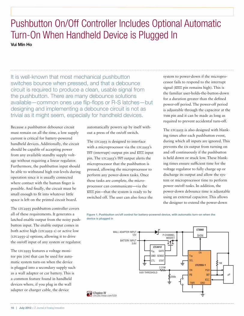
Pushbutton On/Off Controller Includes Optional Automatic Turn-On When Handheld Device is Plugged InVui Min Ho
Because a pushbutton debounce circuit
must remain on all the time, a low supply
current is critical for battery-powered
handheld devices. Additionally, the circuit
should be capable of accepting power
from any available standby supply volt-
age without requiring a linear regulator.
Furthermore, the pushbutton input should
be able to withstand high ESD levels during
operation since it is usually connected
where contact with the human finger is
possible. And finally, the circuit must be
small enough to fit into whatever little
space is left on the printed circuit board.
The LTC2955 pushbutton controller covers
all of these requirements. It generates a
latched enable output from the noisy push-
button input. The enable output comes in
both active high (LTC2955-1) or active low
(LTC2955-2) options, allowing it to drive
the on/off input of any system or regulator.
The LTC2955 features a voltage moni-
tor pin (ON) that can be used for auto-
matic system turn-on when the device
is plugged into a secondary supply such
as a wall adapter or car battery. This is
a common feature found in handheld
devices where, if you plug in the wall
adapter or charger cable, the device
automatically powers up by itself with-
out a press of the on/off switch.
The LTC2955 is designed to interface
with a microprocessor via the LTC2955’s
INT (interrupt) output pin and KILL input
pin. The LTC2955’s INT output alerts the
microprocessor that the pushbutton is
pressed, allowing the microprocessor to
perform any power-down tasks. Once
these tasks are complete, the micro-
processor can communicate—via the
KILL pin—that the system is ready to be
switched off. The user can also force the
system to power-down if the micropro-
cessor fails to respond to the interrupt
signal (KILL pin remains high). This is
the familiar user-holds-the-button-down
for a duration greater than the defined
power-off period. The power-off period
is adjustable through the capacitor at the
TMR pin and it can be made as long as
required to prevent accidental turn-off.
The LTC2955 is also designed with blank-
ing times after each pushbutton event,
during which all inputs are ignored. This
prevents the EN output from turning on
and off continuously if the pushbutton
is held down or stuck low. These blank-
ing times ensure sufficient time for the
voltage regulator to fully charge up or
discharge its output and allow the sys-
tem or microprocessor time to perform
power on/off tasks. In addition, the
power-down debounce time is adjustable
using an external capacitor. This allows
the designer to extend the power-down
It is well-known that most mechanical pushbutton switches bounce when pressed, and that a debounce circuit is required to produce a clean, usable signal from the pushbutton. There are many debounce solutions available—common ones use flip-flops or R-S latches—but designing and implementing a debounce circuit is not as trivial as it might seem, especially for handheld devices.
9.6V THRESHOLD
P-CHANNELMOSFET
PB
PGD
INT
KILL
VIN
SEL
ON
TMR
LTC2955-1
µP
1M
2.21M
200k
WALL ADAPTER INPUT12V
BATTERY INPUT3.6V
GND
EN
SHDN
LT3060
LTC4412
GATE
SENSE
STAT
VIN
GND
CTL
Figure 1. Pushbutton on/off control for battery-powered device, with automatic turn-on when the device is plugged in
LTspice IVcircuits.linear.com/559
July 2012 : LT Journal of Analog Innovation | 11
design features
time in cases where some systems need
more time to perform power-down tasks.
The LTC2955 minimizes components by
operating directly from inputs as low as
a 1.5V single-cell battery up to a 36V mul-
ticell stack—with no additional boost
regulator or LDO required. The low quies-
cent current of 1.2μA extends the battery
life. The device is available in a space-
saving 10-lead 3mm × 2mm DFN pack-
age and 8-lead ThinSOT™ package.
HANDHELD WITH AUTOMATIC TURN-ON WHEN PLUGGED IN
Figure 1 shows a typical LTC2955-1
application for a handheld device. The
3.6V supply is produced directly from the
handheld’s battery; the 12V secondary
supply comes from a wall adapter. Both
the 3.6V and 12V inputs are connected
to the LT3060 regulator input via diode-
OR so that either supply can power the
system. The LTC4412 is an ideal diode
controller that controls the P-channel
MOSFET to reduce the voltage drop across
the diode connected to the 3.6V supply.
The LTC2955-1 ON pin monitors the
12V input through the resistive divider R1
and R2. When the user plugs in the wall
adapter, the 12V supply becomes present.
The LTC2955-1 detects that the ON pin is
high and pulls the EN (enable) pin high
after a 32ms debounce time and turns on
the voltage regulator, applying power to
the system. This allows automatic system
turn-on when the user plugs in the wall
adapter. The system can also be turned on
by pressing the pushbutton. The LTC2955
alerts the microprocessor that the 12V sup-
ply is present or absent by pulling the
PGD output pin high or low, respectively.
PUSHBUTTON PIN ESD PROTECTION
The LTC2955 PB (pushbutton) input
is protected to ESD levels of up to
±25kV HBM with respect to ground. This
protection level exists during all modes
of operation including power-down,
power-up or when the supply is dis-
connected from the battery. When the
pushbutton pin is hit with an ESD strike
during operation, the part remains in
its current logic state. The device does
not reset or latch up and there is no
need to cycle the supply to recover.
VERSATILE PUSHBUTTON INPUT
The LTC2955 requires only a few exter-
nal components for most applications,
as shown in Figure 1. Except for the
logic-level pins used to interface with
the microprocessor, most of the pins can
withstand a maximum voltage of 36V,
precluding the need for external sup-
plies or resistor dividers. Designs remain
flexible in the face of high input sup-
ply voltages, especially when no typical
board-level supply (e.g., 5V) is available.
The PB input is designed to operate in
harsh and noisy environments. The pin
The LTC2955 pushbutton controller generates a latched enable output from the noisy pushbutton input. The enable output comes in both active high or active low options, allowing it to drive the on/off input of any system or regulator.
TOP OF BOARD BOTTOM OF BOARD
TURN ON PULSE SHORT PULSE LONG PULSE
TURNS ON STAYS ON
INTERRUPT INTERRUPT
TURNS OFF
PB
EN
INT
Figure 2. LTC2955-1 waveforms
OPTIONALPULLUPRESISTOR
EXTERNALSUPPLY
LTC2955
PB
VLDO
900k
D1
0.8V
–
+
Figure 3. Pushbutton input
12 | July 2012 : LT Journal of Analog Innovation
can be tied to the external supply through
an optional pull-up resistor as shown.
The ON input and SEL inputs can withstand
voltages up to 36V. This makes it easy to
connect these pins directly to the high volt-
age supply without requiring a resistive
divider, and thus minimize the quiescent
current consumed by the resistive divider.
CONCLUSION
The LTC2955 is a family of micropower
(1.2µA), wide input voltage range (1.5V to
36V) pushbutton controllers. These parts
lower system cost and preserve bat-
tery life by integrating a rugged push-
button input, a flexible enable output
and a simple microprocessor interface
that provides intelligent power-up and
power-down. The device is available
in space-saving 10-lead 3mm × 2mm
DFN and 8-lead ThinSOT packages. n
can withstand both positive and negative
voltages up to ±36V. This allows for long
cable runs between the pushbutton switch
and the LTC2955, where even if the input
rings, it will not cause damage to the part.
Figure 3 shows the pushbutton pin con-
nection and internal circuitry. The internal
900k pull-up resistor allows connection
of the pin directly to the pushbutton
switch (with the other terminal grounded)
without requiring an external pull-up
resistor. If an external pull-up resistor is
desired in applications where the pushbut-
ton switch is leaky, this optional pull-up
resistor can be tied to any voltage up to
the 36V maximum as shown. The internal
diode D1 blocks the external supply cur-
rent from flowing into the device, prevent-
ing unnecessary current consumption.
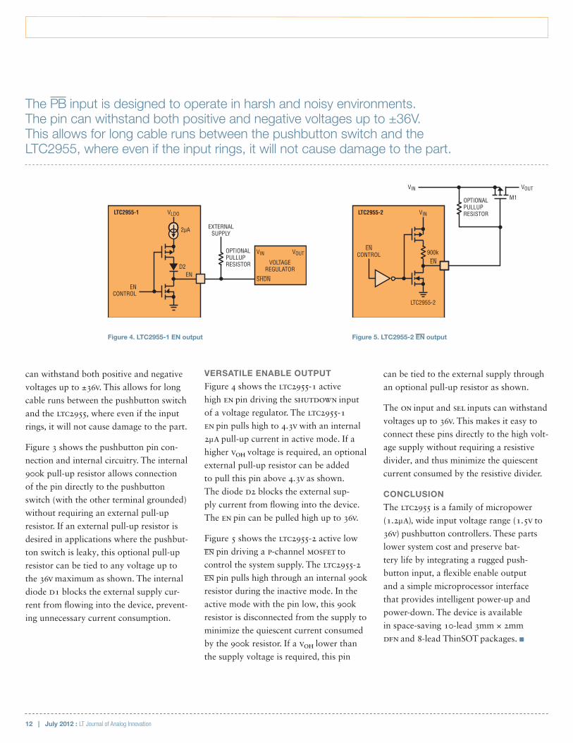
VERSATILE ENABLE OUTPUT
Figure 4 shows the LTC2955-1 active
high EN pin driving the SHUTDOWN input
of a voltage regulator. The LTC2955-1
EN pin pulls high to 4.3V with an internal
2µA pull-up current in active mode. If a
higher VOH voltage is required, an optional
external pull-up resistor can be added
to pull this pin above 4.3V as shown.
The diode D2 blocks the external sup-
ply current from flowing into the device.
The EN pin can be pulled high up to 36V.
Figure 5 shows the LTC2955-2 active low
EN pin driving a P-channel MOSFET to
control the system supply. The LTC2955-2
EN pin pulls high through an internal 900k
resistor during the inactive mode. In the
active mode with the pin low, this 900k
resistor is disconnected from the supply to
minimize the quiescent current consumed
by the 900k resistor. If a VOH lower than
the supply voltage is required, this pin
VLDO
2µA
EN
ENCONTROL
LTC2955-1
VOLTAGEREGULATOR
VIN
D2
SHDN
VOUTOPTIONALPULLUPRESISTOR
EXTERNALSUPPLY
LTC2955-2 VIN
EN
ENCONTROL
LTC2955-2
900k
VOUTVIN
M1OPTIONALPULLUPRESISTOR
Figure 4. LTC2955-1 EN output Figure 5. LTC2955-2 EN output
The PB input is designed to operate in harsh and noisy environments. The pin can withstand both positive and negative voltages up to ±36V. This allows for long cable runs between the pushbutton switch and the LTC2955, where even if the input rings, it will not cause damage to the part.

July 2012 : LT Journal of Analog Innovation | 13
design features
I2C-Controlled Li-Ion Power Management IC with Integrated Power Devices Charges High Capacity Batteries from Any 5V Source While Keeping CoolDavid Simmons
While USB has become the dominant stan-
dard for device interconnect, synchroniza-
tion and data exchange, its power delivery
capabilities have not kept pace with bat-
tery demands. USB 2.0 allows a maximum
2.5W load, while USB 3.0 extends the limit
to 4.5W. Even with perfect efficiency and
all power going directly to the battery,
a full charge cycle via USB would require
overnight and then some. Though USB is
not suitable as a primary power source for
large capacity batteries, it still has great
value as an opportunistic power source
to charge when and where possible, and
to prevent battery drain when the device
is tethered to a traditional computer.
THE BEST OF BOTH WORLDS
The LTC4155 is a monolithic switching
battery charger that delivers 3.5A charge
current efficiently in a compact PCB foot-
print. Figure 1 shows the required com-
ponents in a typical application. The
2.25MHz switching frequency allows for
a small inductor and bypass capacitors
to minimize the overall PCB footprint.
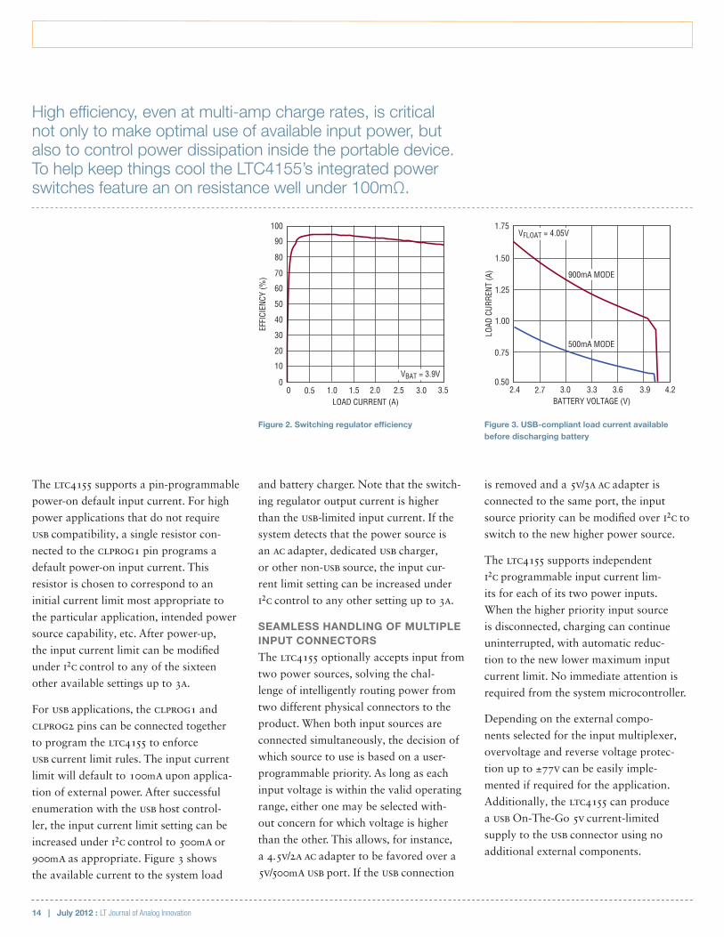
High efficiency (Figure 2) even at multi-
amp charge rates is critical not only to
make optimal use of available input
power, but also to control power dis-
sipation inside the portable device. The
combination of high power dissipa-
tion and marginal thermal performance
in a tightly enclosed space can make
a device with a less efficient charging
solution too warm to hold comfortably.
To help keep things cool, the LTC4155’s
integrated power switches feature an
on-resistance well under 100mΩ.
While the LTC4155’s power switches are
sized to handle higher currents than
available from USB, the LTC4155 remains
fully USB compatible for opportunistic
charging. Input current is automatically
measured internally and limited to any
of sixteen I2C user-selectable values. Of
these settings, three correspond to guar-
anteed maximum limits of 100mA and
500mA for USB 2.0 and 900mA for USB 3.0.
Automatic input current limiting can also
be used with AC adapters or other sources
by choosing any of the other current
limit settings up to a maximum of 3A.
Designers of portable electronics are challenged to create devices that do everything while running endlessly on a single battery charge. While it is impossible to fully meet this challenge, each successive generation of batteries at least comes closer to that goal. With devices now sporting large vibrant touch-sensitive displays, multicore CPU and graphics processors, and an assortment of wireless modems for high speed communications anywhere on the planet, high battery capacity is essential. Battery manufacturers have met the demand with light weight, compact cells with capacities to over 30 watt-hours.
3
499Ω0.047µF
3.6k
1.21k
L1: COILCRAFT XFL4020-102MEMP1: VISHAY Si5481DU-T1-GE3
100k
2.4A
22µF
TOSYSTEMLOAD
10µF
TO µC
TO µC
WALLSNS SW
WALLGT
VBUS
USBGT
USBSNS
CLPROG1 CLPROG2 GND PROGVC
ID NTCBIAS
MP1
BATSNS
BATGATE
L11µH
VOUTSNS
VOUT
CHGSNSLTC4155
I2C
IRQ
OVGCAP NTC
5V INPUT
Li-IONBATTERY
Figure 1. I2C controlled high power battery charger/USB power manager
14 | July 2012 : LT Journal of Analog Innovation
The LTC4155 supports a pin-programmable
power-on default input current. For high
power applications that do not require
USB compatibility, a single resistor con-
nected to the CLPROG1 pin programs a
default power-on input current. This
resistor is chosen to correspond to an
initial current limit most appropriate to
the particular application, intended power
source capability, etc. After power-up,
the input current limit can be modified
under I2C control to any of the sixteen
other available settings up to 3A.
For USB applications, the CLPROG1 and
CLPROG2 pins can be connected together
to program the LTC4155 to enforce
USB current limit rules. The input current
limit will default to 100mA upon applica-
tion of external power. After successful
enumeration with the USB host control-
ler, the input current limit setting can be
increased under I2C control to 500mA or
900mA as appropriate. Figure 3 shows
the available current to the system load
and battery charger. Note that the switch-
ing regulator output current is higher
than the USB-limited input current. If the
system detects that the power source is
an AC adapter, dedicated USB charger,
or other non-USB source, the input cur-
rent limit setting can be increased under
I2C control to any other setting up to 3A.
SEAMLESS HANDLING OF MULTIPLE INPUT CONNECTORS
The LTC4155 optionally accepts input from
two power sources, solving the chal-
lenge of intelligently routing power from
two different physical connectors to the
product. When both input sources are
connected simultaneously, the decision of
which source to use is based on a user-
programmable priority. As long as each
input voltage is within the valid operating
range, either one may be selected with-
out concern for which voltage is higher
than the other. This allows, for instance,
a 4.5V/2A AC adapter to be favored over a
5V/500mA USB port. If the USB connection
is removed and a 5V/3A AC adapter is
connected to the same port, the input
source priority can be modified over I2C to
switch to the new higher power source.
The LTC4155 supports independent
I2C programmable input current lim-
its for each of its two power inputs.
When the higher priority input source
is disconnected, charging can continue
uninterrupted, with automatic reduc-
tion to the new lower maximum input
current limit. No immediate attention is
required from the system microcontroller.
Depending on the external compo-
nents selected for the input multiplexer,
overvoltage and reverse voltage protec-
tion up to ±77V can be easily imple-
mented if required for the application.
Additionally, the LTC4155 can produce
a USB On-The-Go 5V current-limited
supply to the USB connector using no
additional external components.
High efficiency, even at multi-amp charge rates, is critical not only to make optimal use of available input power, but also to control power dissipation inside the portable device. To help keep things cool the LTC4155’s integrated power switches feature an on resistance well under 100mΩ.
LOAD CURRENT (A)0
0
EFFI
CIEN
CY (%
)
10
30
40
50
100
70
1.0 2.0 2.5
20
80
90
60
0.5 1.5 3.0 3.5
VBAT = 3.9V
Figure 2. Switching regulator efficiency
BATTERY VOLTAGE (V)2.4
0.50
LOAD
CUR
RENT
(A)
0.75
1.00
1.25
1.50
1.75
2.7 3.0 3.3 3.6 3.9 4.2
500mA MODE
900mA MODE
VFLOAT = 4.05V
Figure 3. USB-compliant load current available before discharging battery
July 2012 : LT Journal of Analog Innovation | 15
design features
EXTENSIVE PROGRAMMABILITY AND TELEMETRY FOR ADVANCED CHARGING ALGORITHMS
The LTC4155 provides continuous I2C sta-
tus reporting, allowing system software
to have a complete view of the state of
input power sources, fault conditions,
battery charge cycle state, battery tem-
perature, and several other parameters.
Key charge parameters can be changed
under I2C control to implement customized
charge algorithms. Unlike microcontroller-
based or other programmable charge
algorithms, all possible LTC4155 settings
available under software I2C control are
intrinsically safe for the battery. Float
voltage can never be programmed above
4.2V or below 4.05V. Similarly, battery
charge current is programmble to one
of 15 possible settings, but software may
never increase the limit above the level
set by the designer—via a programming
resistor chosen to match the battery
capacity and maximum charge rate.
Continuous battery temperature data is
available to system software to dynami-
cally adapt system or charger behavior
to manage extreme operational cor-
ners. For instance, float voltage and/or
charge current may be reduced under
I2C control to increase the battery safety
margin at high ambient temperatures.
Similarly, charge current or total system
load current can be reduced in response
to high temperature to reduce additional
heating within the product enclosure.
Like all other aspects of battery charger
programmability, the LTC4155 imple-
ments an intrinsically safe charging
solution without (or despite) any soft-
ware intervention. Battery charging is
always paused when the cell tempera-
ture falls below 0°C or rises above 40°C.
Additionally, a fault interrupt may be
optionally generated whenever cell
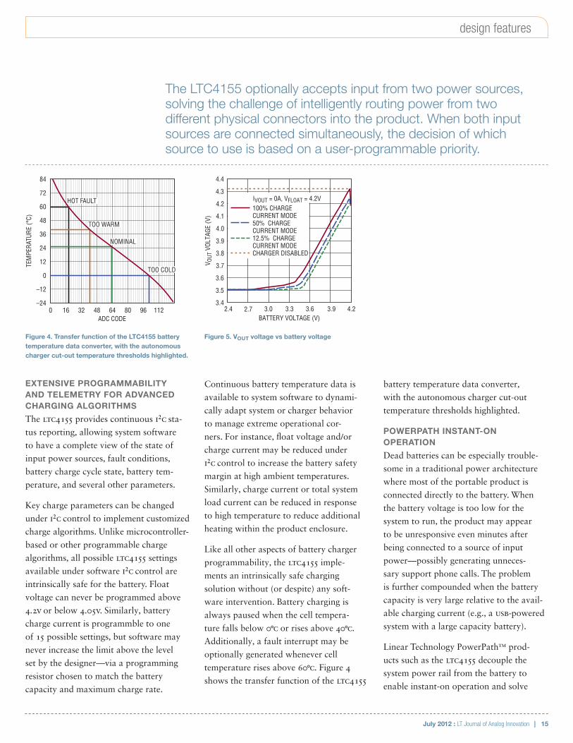
temperature rises above 60°C. Figure 4
shows the transfer function of the LTC4155
battery temperature data converter,
with the autonomous charger cut-out
temperature thresholds highlighted.
POWERPATH INSTANT-ON OPERATION
Dead batteries can be especially trouble-
some in a traditional power architecture
where most of the portable product is
connected directly to the battery. When
the battery voltage is too low for the
system to run, the product may appear
to be unresponsive even minutes after
being connected to a source of input
power—possibly generating unneces-
sary support phone calls. The problem
is further compounded when the battery
capacity is very large relative to the avail-
able charging current (e.g., a USB-powered
system with a large capacity battery).
Linear Technology PowerPath™ prod-
ucts such as the LTC4155 decouple the
system power rail from the battery to
enable instant-on operation and solve
TEM
PERA
TURE
(°C)
ADC CODE 0
84
–2416 32 48 64 80 96 112
–12
0
12
24
36
48
60
72HOT FAULT
TOO COLD
TOO WARM
NOMINAL
Figure 4. Transfer function of the LTC4155 battery temperature data converter, with the autonomous charger cut-out temperature thresholds highlighted.
BATTERY VOLTAGE (V)2.4
3.4
V OUT
VOL
TAGE
(V)
3.6
3.5
3.8
3.7
4.0
3.9
4.2
4.1
4.4
4.3
2.7 3.0 3.3 3.6 3.9 4.2
IVOUT = 0A, VFLOAT = 4.2V100% CHARGE CURRENT MODE50% CHARGE CURRENT MODE12.5% CHARGE CURRENT MODECHARGER DISABLED
Figure 5. VOUT voltage vs battery voltage
The LTC4155 optionally accepts input from two power sources, solving the challenge of intelligently routing power from two different physical connectors into the product. When both input sources are connected simultaneously, the decision of which source to use is based on a user-programmable priority.

16 | July 2012 : LT Journal of Analog Innovation
the two most vexing problems caused
by deeply discharged batteries.
The first problem is that charge current
and system load become indistinguish-
able when the system power rail is
connected directly to the battery. When
the battery is deeply discharged, bat-
tery manufacturers recommend a greatly
reduced initial charge current until the cell
voltage reaches a safer level. This trickle
charge current must be programmed
to a safe level for the battery assuming
minimum or no system load current.
Secondly, in a direct-connect battery
system, if the system is operational dur-
ing trickle charging, a significant portion
of the charge current intended for the
battery is shunted to the system rail. The
resulting reduced battery charge current
extends recovery time proportionately.
A sizable system load can cause the net
battery current to reverse, further dis-
charging the battery. For the duration of
this low battery condition, the portable
system may not be able to respond to
the user due to insufficient voltage on
the system power supply rail. The dura-
tion of unresponsiveness is multiplied
by at least a factor of 10 because of the
reduced power available to the common-
connected battery and system power rail.
The LTC4155 delivers 3.5V to the system
rail when the battery is deeply discharged
to enable instant start-up. As the bat-
tery voltage rises during the precharg-
ing phase, the LTC4155 seamlessly and
automatically transitions to a higher
efficiency mode to speed charging and
minimize heat production. Figure 5 shows
the voltage available to the system power
rail as a function of battery voltage.
The LTC4155 battery charge current is
programmed independently from the input
current limit to decouple battery charge
current constraints from input power
constraints. The input current limit can
be programmed based only on the limita-
tions of the input supply. Similarly, the
battery charge current can be programmed
based only on the battery capacity. The
LTC4155 always enforces input current
limit and prioritizes power to the system
load over battery charging if necessary.
ROBUST IN THE FACE OF NON-IDEAL SOURCES
The LTC4155 features automatic reduction
of input current when the input volt-
age begins to drop to an unacceptable
level. At high charge current levels, this
can happen when connections are made
through undersized wire, to an under-
sized adapter, through connectors with
mild corrosion, or any number of condi-
tions outside the usual design envelope.
Without intervention, the input volt-
age to the IC would continue to drop,
eventually falling below the undervolt-
age lockout threshold. The IC would then
shut down, allowing the input voltage to
recover and restart the whole cycle. The
LTC4155 makes the best of a bad situa-
tion. As the input voltage falls to 4.3V,
the LTC4155 smoothly reduces its input
power by whatever amount is necessary to
prevent further decay of the input volt-
age. In this mode the current delivered to
the system load and battery is less than
the programmed amount, but more than
would be available if the input voltage
oscillation were allowed to continue.
Additionally, the LTC4155 produces an
I2C status report and optional interrupt
signal to alert the system that correc-
tive or diagnostic action may need to be
undertaken by the end user to restore
maximum charge current capability.
CONCLUSION
The LTC4155 combines high current capa-
bility and efficiency with a small mono-
lithic PCB footprint, ideal for portable
devices with large lithium batteries where
board space is at a premium, and heat and
charge time are the enemy. USB-compatible
input current limit settings further extend
versatility to allow opportunistic charg-
ing from ubiquitous but lower power
sources. Extensive telemetry allows for
custom behavior based on changing
environmental or application conditions
without compromising autonomous
battery safety. Uninterrupted power is
delivered to the system rail despite com-
mon problems such as a deeply discharged
battery or a resistive undersized input
power cable. The LTC4155 is available in
a 28-lead 4mm × 5mm QFN package. n
The LTC4155 features automatic reduction of input current when the input voltage begins to drop to an unacceptable level. At high charge current levels, this can happen when connections are made through undersized wire, to an undersized adapter, through connectors with mild corrosion, or other conditions outside the usual design envelope.

July 2012 : LT Journal of Analog Innovation | 17
design features
extends high efficiency operation for
more than two decades of load current.
A feedforward network (CFF, RFF of
Figure 2) connected between the VIN and
FB pins provides improved transient
response when the wall adapter voltage is
applied. Feedforward values were selected
by first measuring the voltage change in
voltage at COMP as VIN transitions from
3.6V to 12V. A 380mV change at COMP was
observed, optimal values for VIN and
RFF can now be calculated as follows:
C VV
C C pFFFCOMP
INFB P= • +( ) =∆
∆33
R R CC
kFFFB FB
FF= • = 681
VOUT regulation is maintained within
300mV or 6% during the 15µs transi-
tion with a 47µF output cap (Figure 4)
and 500mA load. A falling VIN edge is
about 10-times slower, resulting in
an even smaller transient.
A 3.6V input, 5V output load step response
using the compensation components of
Figure 2 is shown in Figure 5. In this
case, a 250mA to 1A load step results in
only a 250mV transient on VOUT with a
47µF output capacitor. Figures 4 and
5 illustrate how the LTC3112’s loop
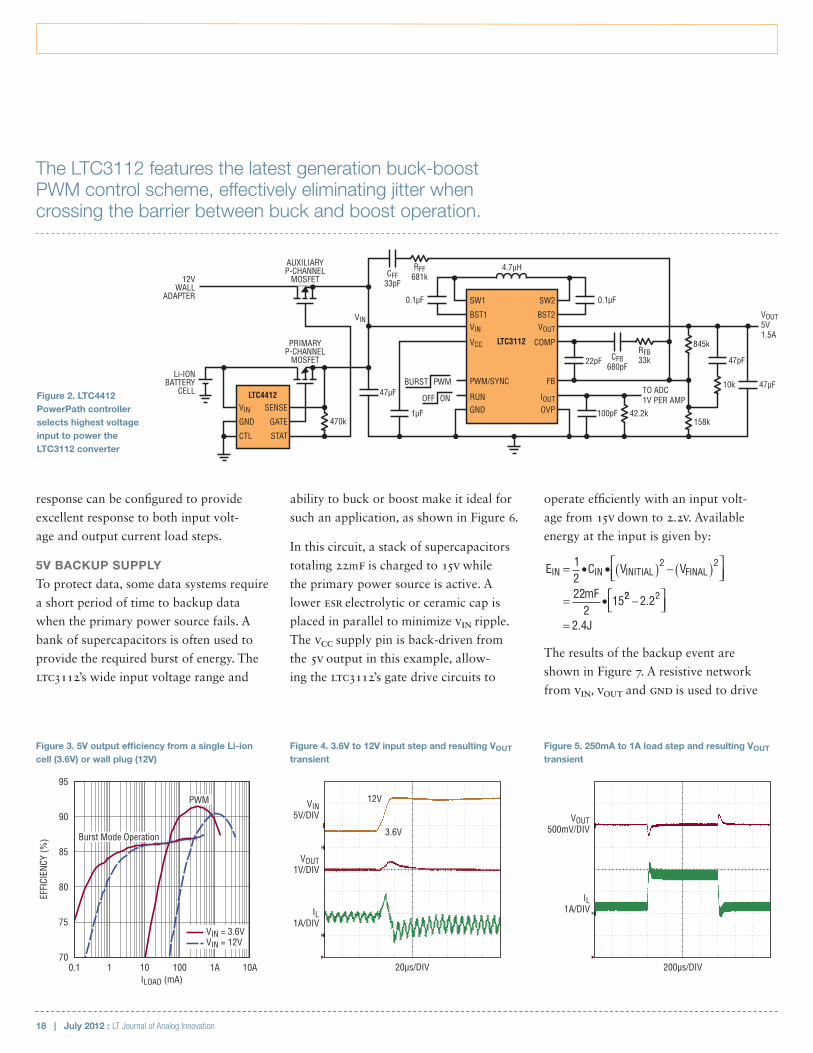
15V, 2.5A Monolithic Buck-Boost DC/DC Converter with 95% Efficiency and Low Noise OperationEddy Wells
The LTC3112 features the latest generation
buck-boost PWM control scheme, effec-
tively eliminating jitter when crossing the
barrier between buck and boost opera-
tion. Safeguards such as current limit,
overvoltage protection, thermal shutdown,
and short-circuit protection provide
robust operation in harsh environments.
For demanding applications where compo-
nent size or conversion efficiency is criti-
cal, the LTC3112’s 750kHz default switching
frequency can be synchronized between
300kHz and 1.5MHz. For designs where
output current needs to be controlled
or measured, an output current monitor
pin is available. Selectable Burst Mode®
operation extends the operating life when
the battery-powered device is idle.
The LTC3112-based converter shown in
Figure 1 can generate 30W of power with
a 12V output. The solution footprint
is less than 200mm2, which cannot be
matched by a controller-based buck-boost
or complex dual-inductor SEPIC design
at similar power levels. The main exter-
nal components are limited to the input
and output filter caps and the power
inductor. The LTC3112 is offered in a
thermally enhanced 16-lead 4mm × 5mm
DFN or 20-lead TSSOP package.
OPERATION FROM MULTIPLE INPUT SOURCES
The LTC3112’s wide operating range allows
devices to be powered from multiple input
sources. Figure 2 shows an application
where the LTC4412 PowerPath control-
ler (TSOT-23 package) provides a low loss
selection between two input sources. The
LTC4412 maintains a 20mV forward voltage
across the selected P-channel MOSFET, keep-
ing losses to a minimum. In this circuit,
the LTC4412 automatically switches the
greater of a single Li-ion cell or 12V wall
adapter to the input of the LTC3112.
Efficiency curves based on the two
input sources are given in Figure 3. Peak
efficiencies of greater than 90% are
achieved with either input. Selectable
Burst Mode operation (dashed lines)
with 50µA of typical sleep current
Power-hungry handheld devices and industrial instruments often require multicell or high capacity batteries to support their ever-increasing processing needs. A wide voltage range, high efficiency buck-boost DC/DC converter is the ideal solution for longer battery run times and handling multiple input sources. The LTC3112 is a 2.2V to 15V input capable 2.5A buck-boost converter. The extended voltage range allows conversion from a variety of power sources such as one, two or three Li-ion cells, lead acid batteries, supercapacitors, USB cables and wall adapters to output voltages programmed between 2.5V and 14V.
Figure 1. LTC3112 based 30W solution
18 | July 2012 : LT Journal of Analog Innovation
ability to buck or boost make it ideal for
such an application, as shown in Figure 6.
In this circuit, a stack of supercapacitors
totaling 22mF is charged to 15V while
the primary power source is active. A
lower ESR electrolytic or ceramic cap is
placed in parallel to minimize VIN ripple.
The VCC supply pin is back-driven from
the 5V output in this example, allow-
ing the LTC3112’s gate drive circuits to
response can be configured to provide
excellent response to both input volt-
age and output current load steps.
5V BACKUP SUPPLY
To protect data, some data systems require
a short period of time to backup data
when the primary power source fails. A
bank of supercapacitors is often used to
provide the required burst of energy. The
LTC3112’s wide input voltage range and
operate efficiently with an input volt-
age from 15V down to 2.2V. Available
energy at the input is given by:
E C V V
mF
IN IN INITIAL FINAL= • • ( ) − ( )
= •
1222
215
2 2
22 22 2
2 4
−
=
.
. J
The results of the backup event are
shown in Figure 7. A resistive network
from VIN, VOUT and GND is used to drive
The LTC3112 features the latest generation buck-boost PWM control scheme, effectively eliminating jitter when crossing the barrier between buck and boost operation.
0.1µF
CFB680pF
VIN
4.7µH
0.1µF
RFB33k
845k
158k
47pF
47µF
1µF
10k
42.2k100pF
TO ADC1V PER AMPONOFF
PWMBURST
SW1
BST1VIN
VCC
RUNGND
PWM/SYNC
SW2
BST2VOUT
COMP
IOUTOVP
FB
LTC3112
VIN SENSE
GND GATE
CTL STAT
LTC4412
VOUT5V1.5A
47µF
CFF33pF
AUXILIARYP-CHANNEL
MOSFET
PRIMARYP-CHANNEL
MOSFET
Li-IONBATTERY
CELL
12VWALL
ADAPTER
RFF681k
22pF
470k
Figure 2. LTC4412 PowerPath controller selects highest voltage input to power the LTC3112 converter
EFFI
CIEN
CY (%
)
ILOAD (mA)10A0.1
95
701 10 100 1A
90
85
80
75VIN = 3.6VVIN = 12V
Burst Mode Operation
PWM VIN5V/DIV
VOUT1V/DIV
IL1A/DIV
20µs/DIV
3.6V
12V
VOUT500mV/DIV
IL1A/DIV
200µs/DIV
Figure 3. 5V output efficiency from a single Li-ion cell (3.6V) or wall plug (12V)
Figure 5. 250mA to 1A load step and resulting VOUT transient
Figure 4. 3.6V to 12V input step and resulting VOUT transient
July 2012 : LT Journal of Analog Innovation | 19
design features
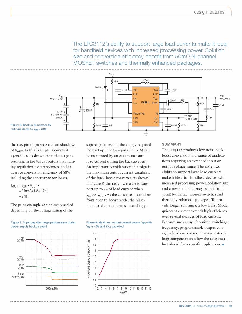
the RUN pin to provide a clean shutdown
of VOUT. In this example, a constant
250mA load is drawn from the LTC3112
resulting in the VIN capacitors maintain-
ing regulation for 1.7 seconds, and an
average conversion efficiency of 88%
including the supercapacitor losses.
E I V tmA V s
J
OUT OUT OUT= • •= • •=
250 5 1 72 1
..
The prior example can be easily scaled
depending on the voltage rating of the
SUMMARY
The LTC3112 produces low noise buck-
boost conversion in a range of applica-
tions requiring an extended input or
output voltage range. The LTC3112’s
ability to support large load currents
make it ideal for handheld devices with
increased processing power. Solution size
and conversion efficiency benefit from
50mΩ N-Channel MOSFET switches and
thermally enhanced packages. To pro-
vide longer run times, a low Burst Mode
quiescent current extends high efficiency
over several decades of load current.
Features such as synchronized switching
frequency, programmable output volt-
age, a load current monitor and external
loop compensation allow the LTC3112 to
be tailored for a specific application. n
supercapacitors and the energy required
for backup. The IOUT pin (Figure 6) can
be monitored by an ADC to measure
load current during the backup event.
An important consideration in design is
the maximum output current capability
of the buck-boost converter. As shown
in Figure 8, the LTC3112 is able to sup-
port up to 4A of load current when
VIN >> VOUT. As the converter transitions
from buck to boost mode, the maxi-
mum load current drops accordingly.
MAX
IMUM
OUT
PUT
CURR
ENT
(A)
VIN (V)152
4.5
03 4 5 6 7 8 9 10 12 1411 13
0.5
1
1.5
2
2.5
3
3.5
4
Figure 8. Maximum output current versus VIN with VOUT = 5V and VCC back-fed
VIN5V/DIV
VOUT5V/DIV
ILOAD500mA/DIV
RUN5V/DIV
500ms/DIV
Figure 7. Supercap discharge performance during power supply backup event
Figure 6. Backup Supply for 5V rail runs down to VIN = 2.2V
0.1µF
680pF
VIN15V TO 2.2V
VOUT
4.7µH
0.1µF
220µF22mFSUPERCAP
STACK
33k845k
158k
47pF47µF
10k
42.2k100pF
TO ADC1V PER AMP
SW1
BST1VIN
VCC
RUNGND
PWM/SYNC
SW2
BST2VOUT
COMP
IOUT
OVP
FB
LTC3112
VOUT5V/500mA
1µF
22pF
499k
1M
499k
++
+
+
BAT54
The LTC3112’s ability to support large load currents make it ideal for handheld devices with increased processing power. Solution size and conversion efficiency benefit from 50mΩ N-channel MOSFET switches and thermally enhanced packages.
20 | July 2012 : LT Journal of Analog Innovation
Novel Current-Sharing IC Balances Two Supplies with EasePinkesh Sachdev
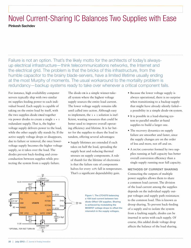
For instance, high availability computer
servers typically ship with two similar
DC supplies feeding power to each indi-
vidual board. Each supply is capable of
taking on the entire load by itself, with
the two supplies diode-ORed together
via power diodes to create a single 1 + 1
redundant supply. That is, the higher
voltage supply delivers power to the load,
while the other supply idly stands by. If the
active supply voltage drops or disappears,
due to failure or removal, the once lower-
voltage supply becomes the higher voltage
supply, so it takes over the load. The
diodes prevent back-feeding and cross-
conduction between supplies while pro-
tecting the system from a supply failure.
The diode-OR is a simple winner-take-
all system where the highest voltage
supply sources the entire load current.
The lower voltage supply remains idle
until called into action. Although easy
to implement, the 1 + 1 solution is inef-
ficient, wasting resources that could be
better used to improve overall operat-
ing efficiency and lifetime. It is far bet-
ter for the supplies to share the load in
tandem, offering several advantages:
•Supply lifetimes are extended if each
takes on half the load, spreading the
supply heat and reducing thermal
stresses on supply components. A rule
of thumb for the lifetime of electronics
is that the failure rate of components
halves for every 10°C fall in temperature.
That’s a significant dependability gain.
•Because the lower voltage supply is
always operational, there is no surprise
when transitioning to a backup supply
that might have already silently failed—
a possibility in a simple diode-OR system.
•It is possible in a load-sharing sys-
tem to parallel smaller at-hand
supplies to build a larger one.
•The recovery dynamics on supply
failure are smoother and faster, since
the supply changes are on the order
of less and more, not off and on.
•A DC/DC converter formed by two sup-
plies running at half capacity has better
overall conversion efficiency than a
single supply running near full capacity.
METHODS OF CURRENT SHARING
Connecting the outputs of multiple
power supplies allows them to share
a common load current. The division
of the load current among the supplies
depends on the individual supply out-
put voltages and supply path resistances
to the common load. This is known as
droop sharing. To prevent back-feeding
of a supply and to isolate the system
from a faulting supply, diodes can be
inserted in series with each supply. Of
course, this added diode voltage drop
affects the balance of the load sharing.SUM85N03-06P+ 25mV –*OPTIONAL, FOR FAST TURN-ON
+ 325mV –SUM85N03-06P
5A
GATE1CPO1
CPO2
GND
EN1
EN2
RANGE
12.2V
11.9V
0.1µF
NC
39nF*
39nF*
VIN1
VCCFETON1
COMP
FETON2
OUT1
OUT2
GATE2VIN2
LTC43702mΩ
2mΩ
0.18µF
11.875V
11.875V
5A
10A
Figure 1. The LTC4370 balancing a 10A load current between two diode-ORed 12V supplies. Sharing is achieved by modulating the MOSFET voltage drops to offset the mismatch in the supply voltages.
Failure is not an option. That’s the likely motto for the architects of today’s always-up electrical infrastructure—think telecommunications networks, the Internet and the electrical grid. The problem is that the bricks of this infrastructure, from the humble capacitor to the brainy blade-servers, have a limited lifetime usually ending at the most Murphy of moments. The usual workaround to the mortality problem is redundancy—backup systems ready to take over whenever a critical component fails.
July 2012 : LT Journal of Analog Innovation | 21
design features
Droop sharing is simple but sharing
accuracy is poorly controlled, and the
series diodes present a voltage and power
loss. A more controlled way of current
sharing is to monitor the supply current,
compare it to an average current required
from each supply, then adjust the supply
voltage (through its trim pin or feedback
network) until the supply current matches
the required value. This method requires
wires to every supply—a share bus—to
signal the current contribution required
from each. The current sharing loop
compensation is customized to accom-
modate the power supply loop dynam-
ics. Controlled current sharing requires
careful design and access to all of the
supplies—not possible in some systems.
This article introduces a new method of
current sharing, allowing active control
of individual supply contributions, but
with the simplicity of droop sharing. In
this system, the diodes are replaced with
adjustable diodes with turn-on voltages
that can be adjusted to achieve balanced
current sharing. This produces better
sharing accuracy than droop sharing
and the power spent in the adjustable
diodes is the minimum required to
achieve sharing, far less than that lost in
a traditional diode. Because no sharing
bus is required, it offers simpler supply-
independent compensation and portable
design. Supplies with difficult or no
access to their trim pins and feedback
networks are ideal for this technique.
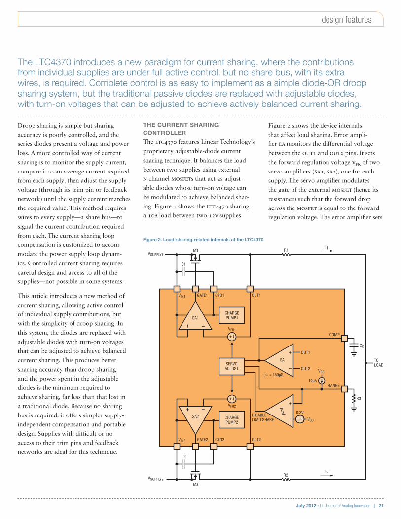
THE CURRENT SHARING CONTROLLER
The LTC4370 features Linear Technology’s
proprietary adjustable-diode current
sharing technique. It balances the load
between two supplies using external
N-channel MOSFETs that act as adjust-
able diodes whose turn-on voltage can
be modulated to achieve balanced shar-
ing. Figure 1 shows the LTC4370 sharing
a 10A load between two 12V supplies
Figure 2 shows the device internals
that affect load sharing. Error ampli-
fier EA monitors the differential voltage
between the OUT1 and OUT2 pins. It sets
the forward regulation voltage VFR of two
servo amplifiers (SA1, SA2), one for each
supply. The servo amplifier modulates
the gate of the external MOSFET (hence its
resistance) such that the forward drop
across the MOSFET is equal to the forward
regulation voltage. The error amplifier sets
CHARGEPUMP1
CHARGEPUMP2
–+SA1
CPO1GATE1VIN1
VCCgm = 150µS
VFR1
VFR2
VCC
VSUPPLY1
OUT1
0.3V
COMP
OUT1
OUT2
RANGE
CPO2GATE2VIN2 OUT2
M1
VSUPPLY2
M2
I2
I1
–+
C1
C2
DISABLELOAD SHARE –
+
–
+CC
10µA
TOLOAD
R3
R1
R2
SERVOADJUST
SA2
EA
+ –+ –
+–
Figure 2. Load-sharing-related internals of the LTC4370
The LTC4370 introduces a new paradigm for current sharing, where the contributions from individual supplies are under full active control, but no share bus, with its extra wires, is required. Complete control is as easy to implement as a simple diode-OR droop sharing system, but the traditional passive diodes are replaced with adjustable diodes, with turn-on voltages that can be adjusted to achieve actively balanced current sharing.
22 | July 2012 : LT Journal of Analog Innovation
the VFR on the lower voltage supply to a
minimum value of 25mV. The servo on the
higher voltage supply is set to 25mV plus
the difference in the two supply volt-
ages. In this way both the OUT pin volt-
ages are equalized. OUT1 = OUT2 implies
I1 • R1 = I2 • R2. Hence, I1 = I2 if R1 = R2.
A simple adjustment to different-valued
sense resistors can be used to set up ratio-
metric sharing, i.e., I1/I2 = R2/R1. Note
that the load voltage tracks 25mV below
the lowest supply voltage.
The MOSFET in conjunction with the servo
amplifier behaves like a diode whose
turn-on voltage is the forward regulation
voltage. The MOSFET is turned off when its
forward drop falls below the regulation
voltage. With increasing MOSFET current,
the gate voltage rises to reduce the on-
resistance to maintain the forward drop
at VFR. This happens until the gate voltage
rails out at 12V above the source. Further
rise in current increases the drop across
the MOSFET linearly as IFET •RDS(ON).
Given the above, when the error ampli-
fier sets the forward regulation voltage
of the servo amplifier, it is functionally
equivalent to adjusting the turn-on voltage
of the (MOSFET-based) diode. The adjust-
ment range runs from a minimum of
25mV to a maximum set by the RANGE pin
(see “Design Considerations” below).
The controller can load share supplies
from 0V to 18V. When both supplies are
below 2.9V, an external supply in the range
2.9V to 6V is required at the VCC pin to
power the LTC4370. Under reverse current
conditions the gate of the MOSFET is turned
off within 1µs. The gate is also turned
on in under a microsecond for a large
forward drop. The fast turn-on, important
for low voltage supplies, is achieved with
a reservoir capacitor on the integrated
charge pump output. It stores charge at
device power-up and delivers 1.4A of gate
pull-up current during a fast turn-on event.
The EN1 and EN2 pins can be used to
turn off their respective MOSFETs. Note
that current can still flow through the
body diode of the MOSFET. When both
channels are off, the device current
consumption is reduced to 80µA per sup-
ply. The FETON outputs indicate whether
the respective MOSFET is on or off.
THE CURRENT SHARING CHARACTERISTIC
Figure 3 shows the current sharing
characteristic of the LTC4370, adjustable-
diode method. There are two plots,
both with the supply voltage difference,
ΔVIN = VIN1 – VIN2, on the x-axis. The
top plot shows the two supply cur-
rents normalized to the load current; the
lower shows the forward voltage drops,
VFWDx, across the MOSFETs. When both
supply voltages are equal (ΔVIN = 0V),
the supply currents are equal, and both
forward voltages are at the minimum
servo voltage of 25mV. As VIN1 increases
above VIN2 (positive ΔVIN), VFWD2 stays
at 25mV, while VFWD1 increases exactly
with ΔVIN to maintain OUT1 = OUT2.
This is turn keeps I1 = I2 = 0.5ILOAD.
There is an upper limit to the adjust-
ment on VFWD set by the RANGE pin. For
the example in Figure 3, that limit is
525mV, set by the RANGE pin at 500mV.
Once VFWD1 hits this limit, sharing
becomes imbalanced and any further
rise in VIN1 pushes OUT1 above OUT2.
The break point is VFR(MAX) – VFR(MIN),
where more of the load current comes
from the higher voltage supply. When
OUT1 – OUT2 = ILOAD •RSENSE, the entire
load current transfers over to I1. This is
the operating point with the maximum
power dissipation in MOSFET M1, since
the entire load current flows through
it with the maximum forward drop.
For example, a 10A load current causes
5.3W (= 10A •525mV) dissipated in the
MOSFET. For any further rise in ΔVIN,
the controller ramps down the forward
DRAWING IS NOT TO SCALE!
–500mV 500mV0
525mV
25mV
MOSFETFORWARDDROP
MAXIMUM M2MOSFET POWERDISSIPATION
VIN1 – VIN2 = ∆VIN
VFWD1VFWD2
VFR(MAX)
VFR(MIN)
IL • RS
–500mV 500mV0
1
0
NORMALIZEDCURRENT
VIN1 – VIN2 = ∆VIN
I2 I1
I1 I2
0.5
SHARING CAPTURE RANGE ±∆VIN(SH)
VRANGE = 500mV
= 2RS1
SLOPE
MAXIMUM M1MOSFET POWERDISSIPATION
Figure 3. Current sharing characteristic of the LTC4370 method as the supply voltage difference varies.
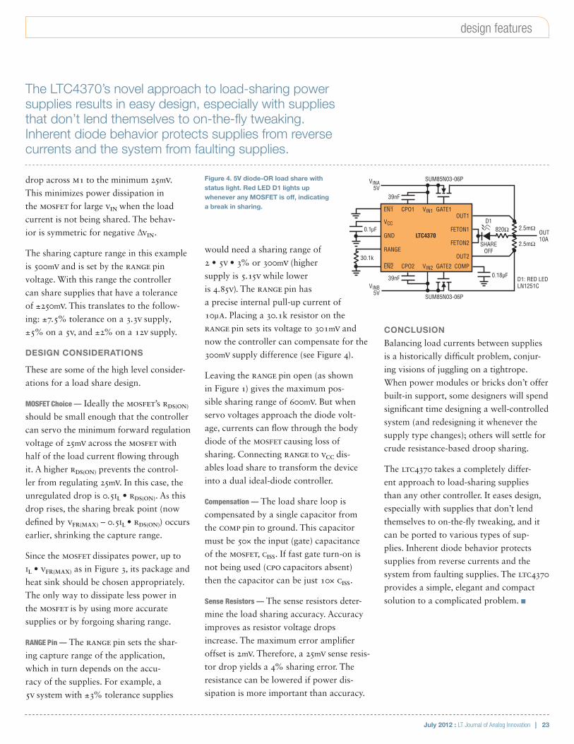
July 2012 : LT Journal of Analog Innovation | 23
design features
drop across M1 to the minimum 25mV.
This minimizes power dissipation in
the MOSFET for large VIN when the load
current is not being shared. The behav-
ior is symmetric for negative ΔVIN.
The sharing capture range in this example
is 500mV and is set by the RANGE pin
voltage. With this range the controller
can share supplies that have a tolerance
of ±250mV. This translates to the follow-
ing: ±7.5% tolerance on a 3.3V supply,
±5% on a 5V, and ±2% on a 12V supply.
DESIGN CONSIDERATIONS
These are some of the high level consider-
ations for a load share design.
MOSFET Choice — Ideally the MOSFET’s RDS(ON)
should be small enough that the controller
can servo the minimum forward regulation
voltage of 25mV across the MOSFET with
half of the load current flowing through
it. A higher RDS(ON) prevents the control-
ler from regulating 25mV. In this case, the
unregulated drop is 0.5IL •RDS(ON). As this
drop rises, the sharing break point (now
defined by VFR(MAX) – 0.5IL •RDS(ON)) occurs
earlier, shrinking the capture range.
Since the MOSFET dissipates power, up to
IL •VFR(MAX) as in Figure 3, its package and
heat sink should be chosen appropriately.
The only way to dissipate less power in
the MOSFET is by using more accurate
supplies or by forgoing sharing range.
RANGE Pin — The RANGE pin sets the shar-
ing capture range of the application,
which in turn depends on the accu-
racy of the supplies. For example, a
5V system with ±3% tolerance supplies
would need a sharing range of
2•5V •3% or 300mV (higher
supply is 5.15V while lower
is 4.85V). The RANGE pin has
a precise internal pull-up current of
10µA. Placing a 30.1k resistor on the
RANGE pin sets its voltage to 301mV and
now the controller can compensate for the
300mV supply difference (see Figure 4).
Leaving the RANGE pin open (as shown
in Figure 1) gives the maximum pos-
sible sharing range of 600mV. But when
servo voltages approach the diode volt-
age, currents can flow through the body
diode of the MOSFET causing loss of
sharing. Connecting RANGE to VCC dis-
ables load share to transform the device
into a dual ideal-diode controller.
Compensation — The load share loop is
compensated by a single capacitor from
the COMP pin to ground. This capacitor
must be 50× the input (gate) capacitance
of the MOSFET, CISS. If fast gate turn-on is
not being used (CPO capacitors absent)
then the capacitor can be just 10× CISS.
Sense Resistors — The sense resistors deter-
mine the load sharing accuracy. Accuracy
improves as resistor voltage drops
increase. The maximum error amplifier
offset is 2mV. Therefore, a 25mV sense resis-
tor drop yields a 4% sharing error. The
resistance can be lowered if power dis-
sipation is more important than accuracy.
CONCLUSION
Balancing load currents between supplies
is a historically difficult problem, conjur-
ing visions of juggling on a tightrope.
When power modules or bricks don’t offer
built-in support, some designers will spend
significant time designing a well-controlled
system (and redesigning it whenever the
supply type changes); others will settle for
crude resistance-based droop sharing.
The LTC4370 takes a completely differ-
ent approach to load-sharing supplies
than any other controller. It eases design,
especially with supplies that don’t lend
themselves to on-the-fly tweaking, and it
can be ported to various types of sup-
plies. Inherent diode behavior protects
supplies from reverse currents and the
system from faulting supplies. The LTC4370
provides a simple, elegant and compact
solution to a complicated problem. n
SUM85N03-06P
D1: RED LEDLN1251C
SHAREOFF
D1
SUM85N03-06P
39nF
GATE1CPO1
CPO2
GND
EN1
EN2
RANGE
VINA5V
VINB5V
0.1µF
30.1k
820Ω
39nF
VIN1
VCCFETON1
COMP
FETON2
OUT1
OUT2
GATE2VIN2
LTC43702.5mΩ
2.5mΩ
OUT10A
0.18µF
Figure 4. 5V diode-OR load share with status light. Red LED D1 lights up whenever any MOSFET is off, indicating a break in sharing.
The LTC4370’s novel approach to load-sharing power supplies results in easy design, especially with supplies that don’t lend themselves to on-the-fly tweaking. Inherent diode behavior protects supplies from reverse currents and the system from faulting supplies.

24 | July 2012 : LT Journal of Analog Innovation
NEW DEMO CIRCUITS
µModule Regulators
•LTM8047: 725V DC isolated low noise
µModule regulator (3.1–29V to 5V at
280mA) www.linear.com/LTM8047
•LTM8048: 725V DC isolated low
noise µModule regulator with
LDO post regulator (3.5V–30V to
5V at 120mA & 5.7V at 120mA)
Monolithic Switching Regulators
•LTC3103: Solar-powered buck supply with
Li battery backup (3.2V–15V to 2.2V at
300mA) www.linear.com/LTC3103
•LTC3115-1: 12V 1MHz buck-boost regulator
with undervoltage lockout (10V–40V to
12V at 1.4A) www.linear.com/LTC3115-1
Switching Regulator Controllers
•LT3798: Isolated no opto-coupler flyback
controller with active power factor
correction (PFC) (90VAC –265VAC to
24V at 2A) www.linear.com/LTC3798
•LT8582: 1.5MHz +5V to ±12V dual
converter (5V to ±12V at 550mA)
www.linear.com/LT8582
•LTC3765/LTC3766: Active clamp
forward converter (18V–72V to
12V at 12.5A) www.linear.com/LTC3765,
www.linear.com/LTC3766
•LTC3838: Dual output, 350kHz, step-down
converter with differential DCR output
sensing (4.5V–38V to 1.2V at 15A &
1.5V & 15A) www.linear.com/LTC3838
•LTC3839: 2MHz, 2-phase, step-down
converter with differential
RSENSE sensing (4.5-14V to 3.3V at 25A)
www.linear.com/LTC3839
•LTC3866: High efficiency,
1.5V/30A step-down converter with
very low DCR Sensing (4.5V–20V to
1.5V at 30A) www.linear.com/LTC3866
LED Drivers
•LT3799-1: Offline isolated flyback
LED controller with active power
factor correction (PFC) (277VAC to
3A/36V) www.linear.com/LTC3799-1
MACRO MODELS
µModule Regulators
•LTM8026: 36V input, 5A CVCC
step-down µModule regulator
www.linear.com/LTM8026
•LTM8029: 36V input, 600mA step-down
µModule converter with 5µA quiescent
current www.linear.com/LTM8029
Monolithic Switching Regulators
•LT3692A: Monolithic dual tracking
3.5A step-down switching regulator
www.linear.com/LT3692A
•LT3973: 42V, 750mA step-down regulator
with 2.5µA quiescent current and inte-
grated diodes www.linear.com/LT3973
•LT3988: Dual 60V monolithic
1A step-down switching regulator
www.linear.com/LT3988
•LT3992: Monolithic dual tracking
3A step-down switching regulator
www.linear.com/LT3992
•LT8610: 42V, 2.5A synchronous step-
down regulator with 2.5µA quiescent
current www.linear.com/LT8610
•LT8611: 42V, 2.5A synchronous
step-down regulator with current
sense and 2.5µA quiescent current
www.linear.com/LT8611
What’s New with LTspice IV?Gabino Alonso
NEW HOW-TO VIDEOS
Evaluating Electrical Quantities
video.linear.com/115
The LTspice IV waveform viewer provides
visual analysis of circuit performance and
performs basic measurements. Sometimes,
though, you need a more in depth numeri-
cal analysis of circuit performance. For
this, .MEASURE statements allow you to
perform direct measurements such as:
•rise, fall and time delay
•average, RMS, min, max
and peak-to-peak
•find X when Y occurs
•derivative and integral evaluations
This new video shows an example
of how to use .MEASURE state-
ments for numerical analysis.
LTspice® IV is a high performance SPICE simulator, schematic capture and waveform viewer designed to speed the process of power supply design. LTspice IV adds enhancements and models to SPICE, significantly reducing simulation time compared to typical SPICE simulators, allowing one to view waveforms for most switching regulators in minutes compared to hours for other SPICE simulators.
LTspice IV is available free from Linear Technology at www.linear.com/LTspice. Included in the download is a complete working version of LTspice IV, macro models for Linear Technology’s power products, over 200 op amp models, as well as models for resistors, transistors and MOSFETs.
What is LTspice IV?
New Video: Evaluating Electrical Quantities

July 2012 : LT Journal of Analog Innovation | 25
design ideas
Follow @LTspice on Twitter for up-to-date information on models, demo circuits, events and user tips: www.twitter.com/LTspice
Differential Amplifiers & ADC Drivers
•LTC6362: Precision, low power rail-to-rail
input/output differential op amp/
SAR ADC driver www.linear.com/LTC6362
System Supervisor, Monitor and Control
•LT4363-2: High voltage surge stopper with
current limit www.linear.com/LT4363
•LTC2960: 36V Nano-current
two input voltage monitor
www.linear.com/LTC2960
•LTC2955-1/-2: Pushbutton on/off
controller with automatic turn-on
www.linear.com/LTC2955 n
LED Drivers
•LT3791: 60V 4-switch synchronous
buck-boost LED driver controller
www.linear.com/LT3791
•LT3796: 100V constant-current and
constant-voltage controller with dual
current sense www.linear.com/LT3796
Inductorless Converters
•LTC3260: Low noise dual supply inverting
charge pump www.linear.com/LTC3260
•LTC3261: High voltage, low quiescent
current inverting charge pump
www.linear.com/LTC3261
•LTC3600: 15V, 1.5A synchronous
rail-to-rail single resistor step-down
regulator www.linear.com/LTC3600
•LTC3630: High efficiency,
65V 500mA synchronous step-down
converter www.linear.com/LTC3630
Switching Regulator Controllers
•LT3798: Isolated no opto-coupler flyback
controller with active power factor
correction (PFC) www.linear.com/LT3798
•LTC3861: Dual, multiphase step-down
voltage mode DC/DC controller
with accurate current sharing
www.linear.com/LTC3861
ANNOTATING SCHEMATIC AND WAVEFORM PLOTS
Adding informative comments to a schematic using text is very useful. However, there are times when adding a line, rectangle, circle or arc to a schematic can better illustrate a circuit. A classic example is highlighting a transformer core using two lines. These graphical annotations are available under Draw in the Edit menu. If you do not want these graphical annotations to snap to the grid, you can hold down the Ctrl key while positioning.
Waveform plots can be annotated with text, arrows, lines, boxes and circles. These annotations are effective for illustrating a particular result in your plot to a colleague. Plot annotations along with Move and Drag can be found under Notes & Annotations under Plot Setting menu. Note that if you annotate a plot you will need to save your annotations via a Plot Setting file (available under Plot Setting menu); otherwise they will not be saved.
Happy simulations!
Power User Tip
Examples of graphical annotations added to a schematic and a waveform plot.

26 | July 2012 : LT Journal of Analog Innovation
frequency is constant over steady state
conditions under line and load. It also
allows the LTC3613 to recover from a large
load step in only a few short cycles. This
architecture yields well balanced current
sharing among multiple LTC3613s, which
can be easily paralleled for high power
applications. It also includes a phase-
lock loop (PLL) for synchronization to an
The LTC3613 monolithic regulator
blurs the line drawn between applica-
tions for controllers and monolithic
regulators by combining a high per-
formance fully featured controller
with onboard low RDS(ON) MOSFETs.
FEATURES
The LTC3613 can accept an input volt-
age between 4.5V to 24V and supports
output voltages between 0.6V to 5.5V. The
onboard top and bottom MOSFETs fea-
ture low RDS(ON), around 7mΩ and 5mΩ,
respectively, keeping power dissipation
low and allowing the LTC3613 to deliver
up to 15A of adjustable load current.
The LTC3613 features true remote differ-
ential output voltage sensing. This allows
for accurate regulation of the output
with maximum load currents and shared
ground planes. This feature is critical for
low output voltage applications, where
even small voltage offsets caused by
parasitic IR drops on board traces can
cost several percentage points in regula-
tion accuracy. Remote differential output
sensing and the LTC3613’s accurate internal
reference combine to offer excellent out-
put regulation accuracy over line, load and
temperature: ±0.25% at 25°C, ±0.67% from
0°C to 85°C and 1% from –40°C to 125°C.
The LTC3613 has a low minimum on-time
of 60ns, allowing for high step-down
ratios at high switching frequencies.
Because of its sophisticated controlled on-
time, valley current mode architecture, the
on-time is controlled so that the switching
24V, 15A Step-Down Regulator in Sub-1mm Height Package Pushes Monolithic Performance LimitsStephanie Dai
Monolithic switching regulators and switching controllers together dominate the DC/DC converter market. Generally, there is little overlap in their respective applications. Controller-based solutions are favored for high performance, higher power applications where minimal power loss and top thermal performance are priorities. In contrast, monolithic regulators are favored in lower power applications where compact size is the main requirement. Controllers typically offer more features than monolithic solutions, but are at a significant solution-size disadvantage. The light footprint of monolithic regulators usually comes at a cost of features and increased power loss, and their reliance on integrated MOSFETs places practical limits on power.
PVIN
SVIN
VOUTPGOOD
RUN
VRNGSENSE–
SENSE+
RPGD100k
INTVCC
RITH28k
RT115k
RDCR3.09k
LTC3613
RFB220k
RFB120k
COUT1330µF2.5V×2
COUT2100µF×2
L10.56µH
SW
DB
CSS0.1µF
RDIV152.3k
RDIV210k
CITH1220pF
CITH2 100pF
3613 F10
VIN6V TO 24V
VOUT1.2V15A
CDCR0.1µF
CB 0.1µF
CVCC4.7µF
CIN1: SANYO 25SVPD82MCOUT1: SANYO 2R5TPE330M9
DB: CENTRAL CMDSH-3L1: VISHAY IHLP4040DZ-056µH
TRACK/SS
ITH
RT
MODE/PLLINEXTVCC
SGND
BOOST
INTVCC INTVCC
PGND
VOSNS+
VOSNS–
CIN210µF
CIN182µF25V
+
+
350kHz
Figure 1. 24V input to 1.2V output using inductor DCR sensing to minimize solution size and cost and to maximize efficiency
LTspice IVcircuits.linear.com/560
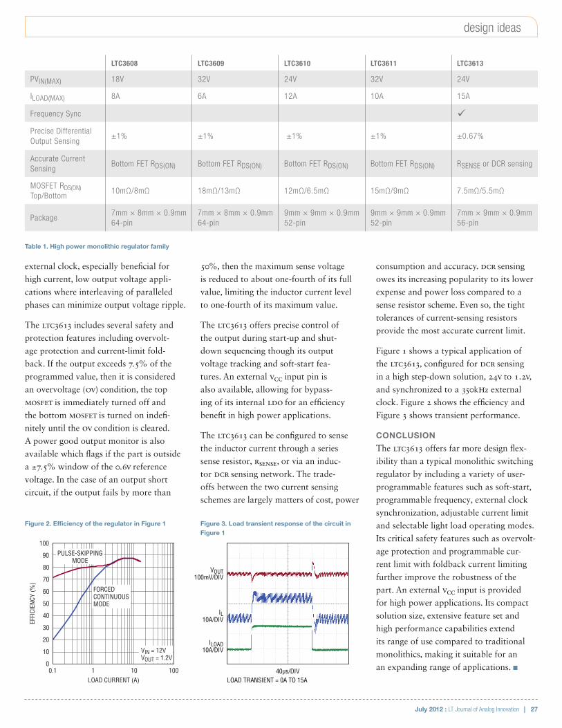
July 2012 : LT Journal of Analog Innovation | 27
design ideas
external clock, especially beneficial for
high current, low output voltage appli-
cations where interleaving of paralleled
phases can minimize output voltage ripple.
The LTC3613 includes several safety and
protection features including overvolt-
age protection and current-limit fold-
back. If the output exceeds 7.5% of the
programmed value, then it is considered
an overvoltage (OV) condition, the top
MOSFET is immediately turned off and
the bottom MOSFET is turned on indefi-
nitely until the OV condition is cleared.
A power good output monitor is also
available which flags if the part is outside
a ±7.5% window of the 0.6V reference
voltage. In the case of an output short
circuit, if the output fails by more than
consumption and accuracy. DCR sensing
owes its increasing popularity to its lower
expense and power loss compared to a
sense resistor scheme. Even so, the tight
tolerances of current-sensing resistors
provide the most accurate current limit.
Figure 1 shows a typical application of
the LTC3613, configured for DCR sensing
in a high step-down solution, 24V to 1.2V,
and synchronized to a 350kHz external
clock. Figure 2 shows the efficiency and
Figure 3 shows transient performance.
CONCLUSION
The LTC3613 offers far more design flex-
ibility than a typical monolithic switching
regulator by including a variety of user-
programmable features such as soft-start,
programmable frequency, external clock
synchronization, adjustable current limit
and selectable light load operating modes.
Its critical safety features such as overvolt-
age protection and programmable cur-
rent limit with foldback current limiting
further improve the robustness of the
part. An external VCC input is provided
for high power applications. Its compact
solution size, extensive feature set and
high performance capabilities extend
its range of use compared to traditional
monolithics, making it suitable for an
an expanding range of applications. n
50%, then the maximum sense voltage
is reduced to about one-fourth of its full
value, limiting the inductor current level
to one-fourth of its maximum value.
The LTC3613 offers precise control of
the output during start-up and shut-
down sequencing though its output
voltage tracking and soft-start fea-
tures. An external VCC input pin is
also available, allowing for bypass-
ing of its internal LDO for an efficiency
benefit in high power applications.
The LTC3613 can be configured to sense
the inductor current through a series
sense resistor, RSENSE, or via an induc-
tor DCR sensing network. The trade-
offs between the two current sensing
schemes are largely matters of cost, power
LOAD CURRENT (A)0.1
40
EFFI
CIEN
CY (%
)
60
70
80
100
1 10 100
20
30
50
90
10
0
VIN = 12VVOUT = 1.2V
PULSE-SKIPPINGMODE
FORCEDCONTINUOUSMODE
Figure 2. Efficiency of the regulator in Figure 1 Figure 3. Load transient response of the circuit in Figure 1
ILOAD10A/DIV
VOUT100mV/DIV
40µs/DIVLOAD TRANSIENT = 0A TO 15AVIN = 12V, VOUT = 1.5VFIGURE 10 CIRCUIT
IL10A/DIV
LTC3608 LTC3609 LTC3610 LTC3611 LTC3613
PVIN(MAX) 18V 32V 24V 32V 24V
ILOAD(MAX) 8A 6A 12A 10A 15A
Frequency Sync
Precise Differential Output Sensing
±1% ±1% ±1% ±1% ±0.67%
Accurate Current Sensing
Bottom FET RDS(ON) Bottom FET RDS(ON) Bottom FET RDS(ON) Bottom FET RDS(ON) RSENSE or DCR sensing
MOSFET RDS(ON) Top/Bottom
10mΩ/8mΩ 18mΩ/13mΩ 12mΩ/6.5mΩ 15mΩ/9mΩ 7.5mΩ/5.5mΩ
Package7mm × 8mm × 0.9mm 64-pin
7mm × 8mm × 0.9mm 64-pin
9mm × 9mm × 0.9mm 52-pin
9mm × 9mm × 0.9mm 52-pin
7mm × 9mm × 0.9mm 56-pin
Table 1. High power monolithic regulator family
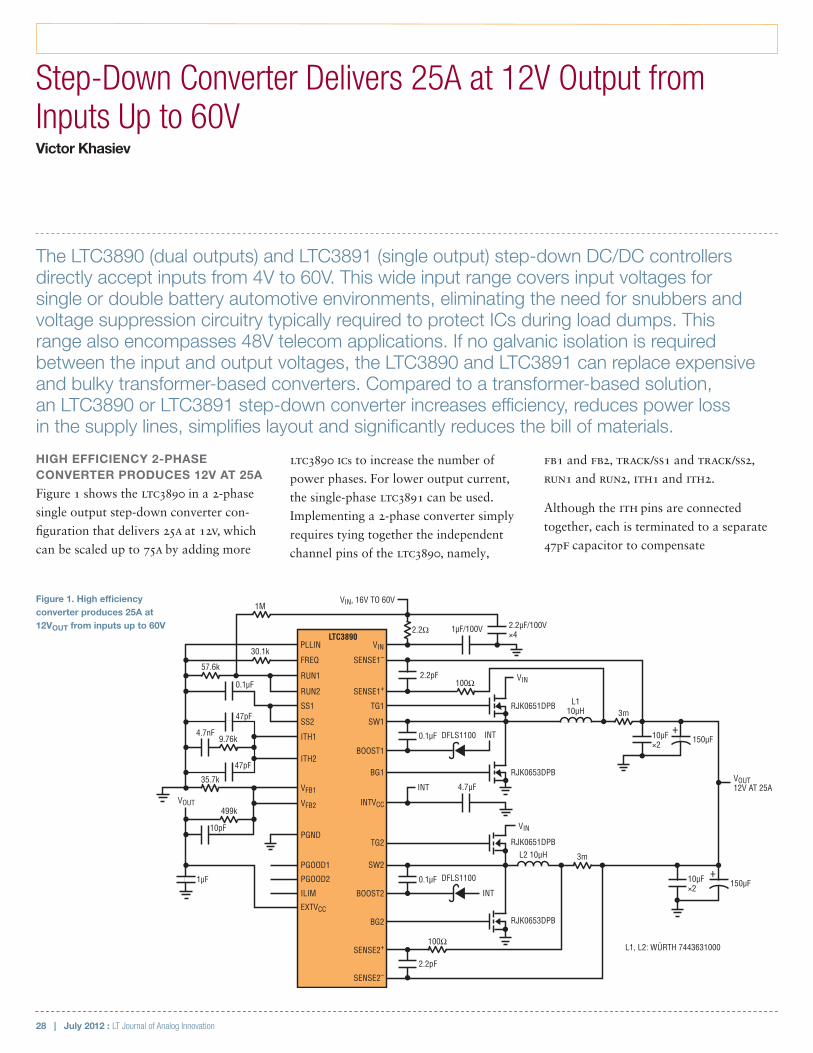
28 | July 2012 : LT Journal of Analog Innovation
FB1 and FB2, TRACK/SS1 and TRACK/SS2,
RUN1 and RUN2, ITH1 and ITH2.
Although the ITH pins are connected
together, each is terminated to a separate
47pF capacitor to compensate
HIGH EFFICIENCY 2-PHASE CONVERTER PRODUCES 12V AT 25A
Figure 1 shows the LTC3890 in a 2-phase
single output step-down converter con-
figuration that delivers 25A at 12V, which
can be scaled up to 75A by adding more
LTC3890 ICs to increase the number of
power phases. For lower output current,
the single-phase LTC3891 can be used.
Implementing a 2-phase converter simply
requires tying together the independent
channel pins of the LTC3890, namely,
Step-Down Converter Delivers 25A at 12V Output from Inputs Up to 60VVictor Khasiev
The LTC3890 (dual outputs) and LTC3891 (single output) step-down DC/DC controllers directly accept inputs from 4V to 60V. This wide input range covers input voltages for single or double battery automotive environments, eliminating the need for snubbers and voltage suppression circuitry typically required to protect ICs during load dumps. This range also encompasses 48V telecom applications. If no galvanic isolation is required between the input and output voltages, the LTC3890 and LTC3891 can replace expensive and bulky transformer-based converters. Compared to a transformer-based solution, an LTC3890 or LTC3891 step-down converter increases efficiency, reduces power loss in the supply lines, simplifies layout and significantly reduces the bill of materials.
Figure 1. High efficiency converter produces 25A at 12VOUT from inputs up to 60V
2.2pF
0.1µF 150µF
0.1µF
2.2pF
DFLS1100
1µF/100V 2.2µF/100V×4LTC3890
35.7k
PLLIN
FREQ
RUN1
RUN2
SS1
SS2
ITH1
ITH2
RJK0651DPB
RJK0653DPB
RJK0651DPB
RJK0653DPB
1M
30.1k
57.6k
9.76k
0.1µF
47pF
47pF
10pF
1µF
4.7nF
VFB1
VFB2
PGND
PGOOD1
PGOOD2
ILIM
EXTVCC
VIN
SENSE1–
SENSE1+
TG1
SW1
BOOST1
BG1
INTVCC
TG2
SW2
BOOST2
BG2
SENSE2+
SENSE2–
499kVOUT
4.7µF
2.2Ω
VIN
VIN, 16V TO 60V
100Ω
INT
INT
DFLS1100
INT
100Ω
3m
3mL2 10µH
L110µH
10µF×2
VOUT12V AT 25A
+
150µF
L1, L2: WÜRTH 7443631000
10µF×2
+
VIN
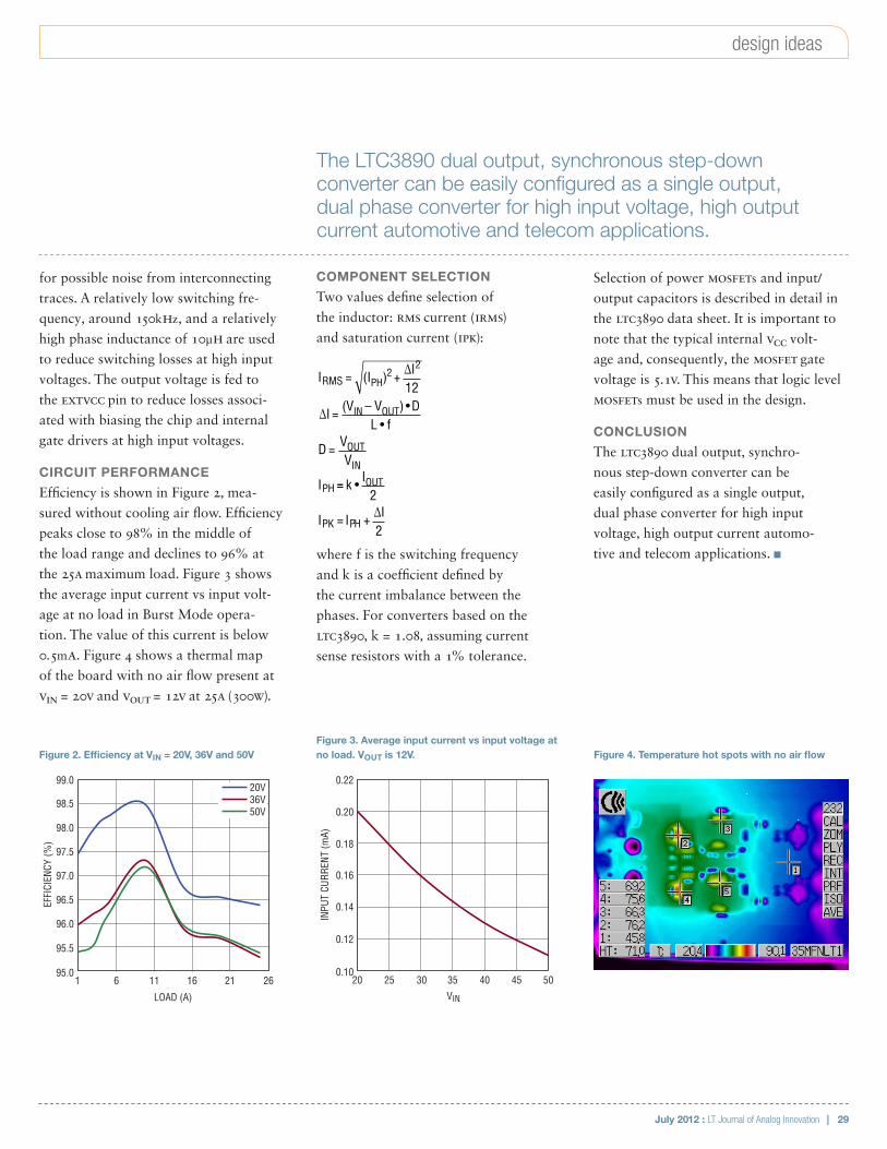
July 2012 : LT Journal of Analog Innovation | 29
design ideas
for possible noise from interconnecting
traces. A relatively low switching fre-
quency, around 150kHz, and a relatively
high phase inductance of 10µH are used
to reduce switching losses at high input
voltages. The output voltage is fed to
the EXTVCC pin to reduce losses associ-
ated with biasing the chip and internal
gate drivers at high input voltages.
CIRCUIT PERFORMANCE
Efficiency is shown in Figure 2, mea-
sured without cooling air flow. Efficiency
peaks close to 98% in the middle of
the load range and declines to 96% at
the 25A maximum load. Figure 3 shows
the average input current vs input volt-
age at no load in Burst Mode opera-
tion. The value of this current is below
0.5mA. Figure 4 shows a thermal map
of the board with no air flow present at
VIN = 20V and VOUT = 12V at 25A (300W).
COMPONENT SELECTION
Two values define selection of
the inductor: RMS current (IRMS)
and saturation current (IPK):
I = (I ) + ∆I12
∆I = (V – V ) •DL • f
D = VV
I
RMS
PH
PH2
2
IN OUT
OUT
IN
== k • I2
I = I + ∆I2
OUT
PK PH
where f is the switching frequency
and k is a coefficient defined by
the current imbalance between the
phases. For converters based on the
LTC3890, k = 1.08, assuming current
sense resistors with a 1% tolerance.
Selection of power MOSFETs and input/
output capacitors is described in detail in
the LTC3890 data sheet. It is important to
note that the typical internal VCC volt-
age and, consequently, the MOSFET gate
voltage is 5.1V. This means that logic level
MOSFETs must be used in the design.
CONCLUSION
The LTC3890 dual output, synchro-
nous step-down converter can be
easily configured as a single output,
dual phase converter for high input
voltage, high output current automo-
tive and telecom applications. n
The LTC3890 dual output, synchronous step-down converter can be easily configured as a single output, dual phase converter for high input voltage, high output current automotive and telecom applications.
Figure 4. Temperature hot spots with no air flow Figure 3. Average input current vs input voltage at no load. VOUT is 12V.Figure 2. Efficiency at VIN = 20V, 36V and 50V
302520 35 40 45 50
0.22
0.20
0.18
0.16
0.14
0.12
0.10
VIN
INPU
T CU
RREN
T (m
A)
LOAD (A)
EFFI
CIEN
CY (%
)
1161 16 21 26
99.0
98.5
98.0
97.5
97.0
96.5
96.0
95.5
95.0
20V36V50V
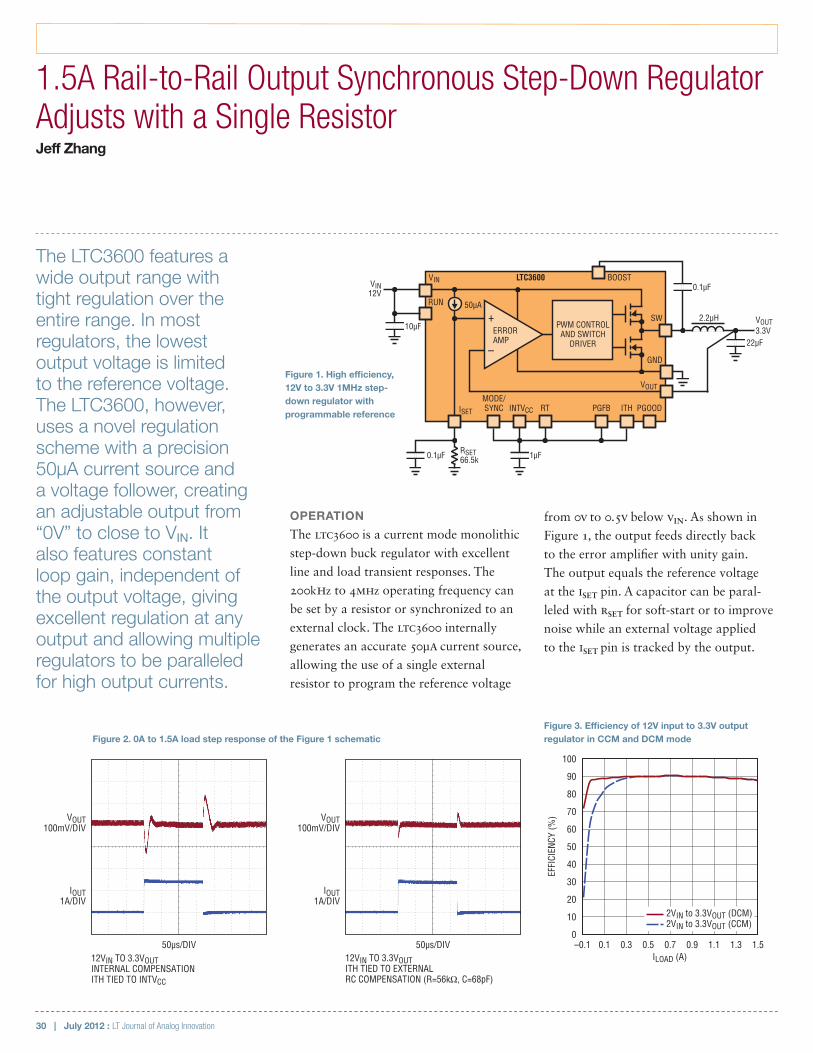
30 | July 2012 : LT Journal of Analog Innovation
OPERATION
The LTC3600 is a current mode monolithic
step-down buck regulator with excellent
line and load transient responses. The
200kHz to 4MHz operating frequency can
be set by a resistor or synchronized to an
external clock. The LTC3600 internally
generates an accurate 50μA current source,
allowing the use of a single external
resistor to program the reference voltage
from 0V to 0.5V below VIN. As shown in
Figure 1, the output feeds directly back
to the error amplifier with unity gain.
The output equals the reference voltage
at the ISET pin. A capacitor can be paral-
leled with RSET for soft-start or to improve
noise while an external voltage applied
to the ISET pin is tracked by the output.
The LTC3600 features a wide output range with tight regulation over the entire range. In most regulators, the lowest output voltage is limited to the reference voltage. The LTC3600, however, uses a novel regulation scheme with a precision 50µA current source and a voltage follower, creating an adjustable output from “0V” to close to VIN. It also features constant loop gain, independent of the output voltage, giving excellent regulation at any output and allowing multiple regulators to be paralleled for high output currents.
1.5A Rail-to-Rail Output Synchronous Step-Down Regulator Adjusts with a Single ResistorJeff Zhang
Figure 3. Efficiency of 12V input to 3.3V output regulator in CCM and DCM mode
EFFI
CIEN
CY (%
)
ILOAD (A)1.5–0.1
100
00.1 0.3 0.5 0.7 0.9 1.1 1.3
10
20
30
40
50
60
70
80
90
2VIN to 3.3VOUT (DCM)2VIN to 3.3VOUT (CCM)
Figure 2. 0A to 1.5A load step response of the Figure 1 schematic
50µs/DIV
VOUT100mV/DIV
IOUT1A/DIV
12VIN TO 3.3VOUTINTERNAL COMPENSATIONITH TIED TO INTVCC
50µs/DIV
VOUT100mV/DIV
IOUT1A/DIV
12VIN TO 3.3VOUTITH TIED TO EXTERNAL RC COMPENSATION (R=56kΩ, C=68pF)
Figure 1. High efficiency, 12V to 3.3V 1MHz step-down regulator with programmable reference
50µA
10µF
1µF
0.1µF
22µF
2.2µH
VIN12V
VOUT
VOUT3.3V
VIN
INTVCCISET RT PGFB ITH PGOOD
RUN
BOOST
SW
GND
LTC3600
MODE/SYNC
0.1µF RSET66.5k
PWM CONTROLAND SWITCH
DRIVER–
+ERRORAMP
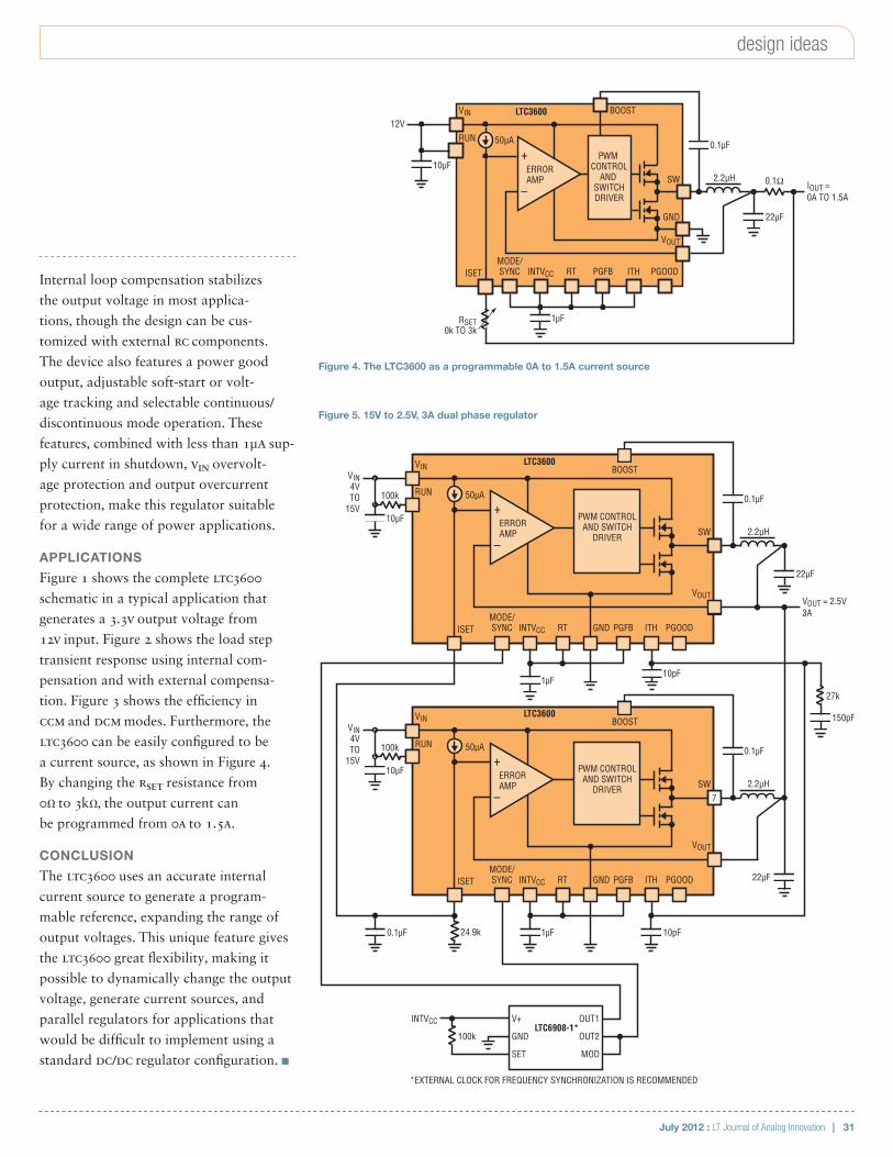
July 2012 : LT Journal of Analog Innovation | 31
design ideas
Internal loop compensation stabilizes
the output voltage in most applica-
tions, though the design can be cus-
tomized with external RC components.
The device also features a power good
output, adjustable soft-start or volt-
age tracking and selectable continuous/
discontinuous mode operation. These
features, combined with less than 1μA sup-
ply current in shutdown, VIN overvolt-
age protection and output overcurrent
protection, make this regulator suitable
for a wide range of power applications.
APPLICATIONS
Figure 1 shows the complete LTC3600
schematic in a typical application that
generates a 3.3V output voltage from
12V input. Figure 2 shows the load step
transient response using internal com-
pensation and with external compensa-
tion. Figure 3 shows the efficiency in
CCM and DCM modes. Furthermore, the
LTC3600 can be easily configured to be
a current source, as shown in Figure 4.
By changing the RSET resistance from
0Ω to 3kΩ, the output current can
be programmed from 0A to 1.5A.
CONCLUSION
The LTC3600 uses an accurate internal
current source to generate a program-
mable reference, expanding the range of
output voltages. This unique feature gives
the LTC3600 great flexibility, making it
possible to dynamically change the output
voltage, generate current sources, and
parallel regulators for applications that
would be difficult to implement using a
standard DC/DC regulator configuration. n
Figure 4. The LTC3600 as a programmable 0A to 1.5A current source
50µA
10µF
0.1µF
0.1Ω
22µF
2.2µH
VIN
ISET
RUN
BOOST
SW
LTC3600
PWM CONTROL
AND SWITCHDRIVER
VOUT
RSET0k TO 3k
12V
1µF
INTVCC RT PGFB ITH PGOODMODE/SYNC
IOUT = 0A TO 1.5A
GND
–
+ERRORAMP
50µA
10µF
0.1µF
2.2µH
VIN
ISET
RUN
BOOST
SW
LTC3600
24.9k
PWM CONTROLAND SWITCH
DRIVER
50µA
10µF
0.1µF
22µF
2.2µH
VIN
ISET
RUN
BOOST
SW
LTC3600
PWM CONTROLAND SWITCH
DRIVER
22µF
VOUT
8
5
7
9
1
11
VOUT
1µF
INTVCC RT PGFB ITH PGOODMODE/SYNC
0.1µF 10pF
6 10 3
GND
13 4 2 12
1µF
100k
INTVCC RT PGFB ITH PGOODMODE/SYNC
10pF
100k
GND
VOUT = 2.5V3A
OUT1
OUT2
MOD
V+
GND
SET
INTVCCLTC6908-1*
*EXTERNAL CLOCK FOR FREQUENCY SYNCHRONIZATION IS RECOMMENDED
100k
27k
150pF
–
+ERRORAMP
–
+ERRORAMP
VIN4VTO
15V
VIN4VTO
15V
Figure 5. 15V to 2.5V, 3A dual phase regulator
highlights from circuits.linear.com
Linear Technology Corporation 1630 McCarthy Boulevard, Milpitas, CA 95035 (408) 432-1900 www.linear.com Cert no. SW-COC-001530
L, LT, LTC, LTM, Linear Technology, the Linear logo, LTspice, Burst Mode, and µModule are registered trademarks, and PowerPath and ThinSOT are trademarks of Linear Technology Corporation. All other trademarks are the property of their respective owners. © 2012 Linear Technology Corporation/Printed in U.S.A./55.8K
LOW NOISE ±12V POWER SUPPLY FROM A SINGLE-ENDED 15V INPUT SUPPLYThe LTC3260 is a low noise dual polarity output power supply that includes an inverting charge pump with both positive and negative LDO regulators. The charge pump operates over a wide 4.5V to 32V input range and can deliver up to 100mA of output current. Each LDO regulator can provide up to 50mA of output current. The negative LDO post regulator is powered from the charge pump output. The LDO output voltages can be adjusted using external resistor dividers.circuits.linear.com/556
LTspice IVcircuits.linear.com/556
OVERVOLTAGE REGULATOR WITH 250V SURGE PROTECTIONThe LT4363 surge stopper protects loads from high voltage transients. It regulates the output during an overvoltage event, such as load dump in vehicles, by controlling the gate of an external N-channel MOSFET. The output is limited to a safe value, allowing the loads to continue functioning. The LT4363 also monitors the voltage drop between the SNS and OUT pins to protect against overcurrent faults. An internal amplifier limits the voltage across the current sense resistor to 50mV. In either fault condition, a timer is started inversely proportional to MOSFET stress. Before the timer expires, the FLT pin pulls low to warn of an impending power-down. If the condition persists, the MOSFET is turned off. The LT4363-1 remains off until reset, whereas the LT4363-2 restarts after a cooldown period.circuits.linear.com/529
LTspice IVcircuits.linear.com/529
36V INPUT, 5.6A TWO 2.5V SERIES SUPERCAPACITOR CHARGERThe LTM8026 is a 36V input, 5A constant-voltage, constant-current (CVCC) step-down µModule regulator. Included in the package are the switching controller, power switches, inductor and support components. Operating over an input voltage range of 6V to 36V, the LTM8026 supports an output voltage range of 1.2V to 24V. CVCC operation allows the LTM8026 to accurately regulate its output current up to 5A over the entire output range. The output current can be set by a control voltage, a single resistor or a thermistor. Only resistors to set the output voltage and frequency and the bulk input and output filter capacitors are needed to complete the design.circuits.linear.com/543
LTspice IVcircuits.linear.com/543
10µF
10nF
10nF
10µF
1µF
10µF10µF
909k
200k
909k
100k
100k
12V
–12V
LDO+15V
LDO–
ADJ+
LTC3260
RT
ADJ–
GND
BYP+
BYP–
VIN
VOUT
EN+
C–
MODE
EN–
C+
0.1µF
10Ω
RSNS10mΩ
Q1FDB33N25
MPS-A42
VIN12V
LT4363DE-2
GND TMR
OUTGATE SNS
UV
SHDN
OV FAULT
OUTPUT CLAMP AT 16V
ENOUT
FLT
FB
D1*SMAJ58A
*DIODES INC.
22µF
0.1µF VCC
DC/DCCONVERTER
GNDSHDN
VCC4.99k
127k
49.9k
57.6k47nF
49.9k
VIN
RUN510k
SS
LTM8026
SYNC
2.5V 2.2F
2.5V 2.2F
10µF
VIN7V TO 36V
VOUT5V
COMP
VOUT
VREF
CTL_I
CTL_TRT GND
68.1k 3.09k
47µF
ADJ


![Atmel ATA6286-EK3 Active RFID Evaluation Kitcn.21ic.com/ebook_download/microsite/Atmel/Atmel-9289... · 2014. 8. 7. · Atmel ATAN0057 [APPLICATION NOTE] 5 9289C–RFID–06/13 2.2](https://img.pdfslide.us/doc/110x75/5fef241de26eee4ac3452f66/atmel-ata6286-ek3-active-rfid-evaluation-kitcn21iccomebookdownloadmicrositeatmelatmel-9289.jpg)


![Atmel ATAN0075 RFID Kits Introduction - 21iccn.21ic.com/ebook_download/microsite/Atmel/Atmel... · Atmel ATAN0075 [APPLICATION NOTE] 9 4980F–RFID–06/13 3. Active RFID Kit ATA6286-EK3](https://img.pdfslide.us/doc/110x75/5f05568f7e708231d41278a6/atmel-atan0075-rfid-kits-introduction-21iccn21iccomebookdownloadmicrositeatmelatmel.jpg)


![User Guide for Car Access Reference System Kit with 1-way RFcn.21ic.com/ebook_download/microsite/Atmel/doc9253.pdf · Atmel ATAN0002: ATAK51001-V1 [APPLICATION NOTE] 2 9253A–RKE–11/11](https://img.pdfslide.us/doc/110x75/5f30c97f2fd36b2a5c5a7023/user-guide-for-car-access-reference-system-kit-with-1-way-rfcn21iccomebookdownloadmicrositeatmel.jpg)