Embed Size (px)
Citation preview
16 V, 4 MHz RR0 Amplifiers AD8665/AD8666/AD8668
Rev. B Information furnished by Analog Devices is believed to be accurate and reliable. However, no responsibility is assumed by Analog Devices for its use, nor for any infringements of patents or other rights of third parties that may result from its use. Specifications subject to change without notice. No license is granted by implication or otherwise under any patent or patent rights of Analog Devices. Trademarks and registered trademarks are the property of their respective owners.
One Technology Way, P.O. Box 9106, Norwood, MA 02062-9106, U.S.A. Tel: 781.329.4700 www.analog.com Fax: 781.461.3113 ©2006–2011 Analog Devices, Inc. All rights reserved.
FEATURES Offset voltage: 2.5 mV max Low input bias current: 1 pA max Single-supply operation: 5 V to 16 V Dual-supply operation: ±2.5 V to ±8 V Low noise: 8 nV/√Hz @ 10 kHz Wide bandwidth: 4 MHz Rail-to-rail output Unity-gain stable Lead-free packaging AD8666/AD8668 qualified for automotive applications
APPLICATIONS Sensor amplification Reference buffers Medical equipment Physiological measurements Signal filters and conditioning Consumer audio Photodiode amplification ADC driver Level shifting circuits
GENERAL DESCRIPTION The AD866x family is single supply, rail-to-rail output amplifiers with low noise performance featuring an extended operating range with supply voltages up to 16 V. They also feature low input bias currents, wide signal bandwidth, and low input voltage and current noise. For lower offset voltage, choose the AD8661/AD8662/AD8664 family.
The combination of low offsets, very low input bias currents, and wide supply range make these amplifiers useful in a wide variety of cost sensitive applications normally associated with much higher priced JFET amplifiers. Systems using high impedance sensors, such as photo diodes, benefit from the combination of low input bias current, low noise, and low offset and bandwidth. The wide operating voltage range matches high performance ADCs and DACs. Audio applications and medical monitoring equipment can take advantage of the high input impedance, low voltage and current noise, wide bandwidth, and the lack of popcorn noise found in many other low input bias current amplifiers.
The AD866x family is specified over the extended industrial temperature range (−40°C to +125°C). See the Ordering Guide for automotive models.
PIN CONFIGURATIONS
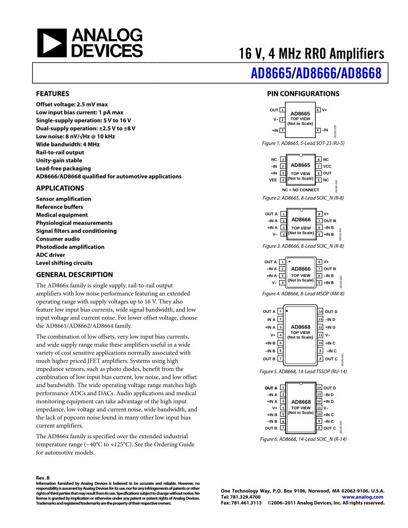
Figure 1. AD8665, 5-Lead SOT-23 (RJ-5)
Figure 2. AD8665, 8-Lead SOIC_N (R-8)
Figure 3. AD8666, 8-Lead SOIC_N (R-8)
Figure 4. AD8666, 8-Lead MSOP (RM-8)
Figure 5. AD8668, 14-Lead TSSOP (RU-14)
Figure 6. AD8668, 14-Lead SOIC_N (R-14)
1
2
3
5
4 –IN+IN
V+OUTAD8665TOP VIEW
(Not to Scale)V–
0619
5-03
9
NC 1
–IN 2
+IN 3
VEE 4
NC8
VCC7
OUT6
NC5
AD8665TOP VIEW
(Not to Scale)
NC = NO CONNECT 0619
5-04
0
OUT A 1
–IN A 2
+IN A 3
V– 4
V+8
OUT B7
–IN B6
+IN B5
AD8666TOP VIEW
(Not to Scale)
0601
8-00
1
OUT A 1
–IN A 2
+IN A 3
V– 4
V+8
OUT B7
–IN B6
+IN B5
AD8666TOP VIEW
(Not to Scale)
0619
5-00
2
1
2
3
4
5
6
7
AD8668IN A
+IN A
V+
OUT B
–IN B
+IN B
OUT A 14
13
12
11
10
9
8
–IN D
+IN D
V–
OUT C
–IN C
+IN C
OUT D
TOP VIEW(Not to Scale)
0619
5-00
3
OUT A–IN A+IN A
V+
OUT D–IN D+IN DV–
+IN B +IN C–IN B
OUT B–IN COUT C
AD8648TOP VIEW
(Not to Scale)
OUT A
AD8668TOP VIEW
(Not to Scale)
AD8648TOP VIEW
(Not to Scale)
6
1
2
3
4
5
7
14
13
12
11
10
9
8
AD8668TOP VIEW
(Not to Scale)
0619
5-00
4
AD8665/AD8666/AD8668
Rev. B | Page 2 of 16
TABLE OF CONTENTS Features .............................................................................................. 1 Applications ....................................................................................... 1 General Description ......................................................................... 1 Pin Configurations ........................................................................... 1 Revision History ............................................................................... 2 Specifications ..................................................................................... 3
Absolute Maximum Ratings ............................................................5 Thermal Resistance .......................................................................5 ESD Caution...................................................................................5
Typical Performance Characteristics ..............................................6 Outline Dimensions ....................................................................... 12
Ordering Guide .......................................................................... 14
REVISION HISTORY 7/11—Rev. A to Rev. B
Change to Features and General Description Sections ............... 1 Updated Outline Dimensions ....................................................... 12 Changes to Ordering Guide .......................................................... 13 Added Automotive Products Section........................................... 13
10/06—Rev. 0 to Rev. A
Added AD8665 ................................................................... Universal Added New Figure 1 and Figure 2, Renumbered Sequentially ................................................................ 1 Changes to Table 4 ............................................................................ 5 Changes to Figure 8, Figure 9, and Figure 11 ............................... 6 Change to Figure 40 ....................................................................... 11 Updated Outline Dimensions ....................................................... 12 Changes to Ordering Guide .......................................................... 13
4/06—Rev 0: Initial Version
AD8665/AD8666/AD8668
Rev. B | Page 3 of 16
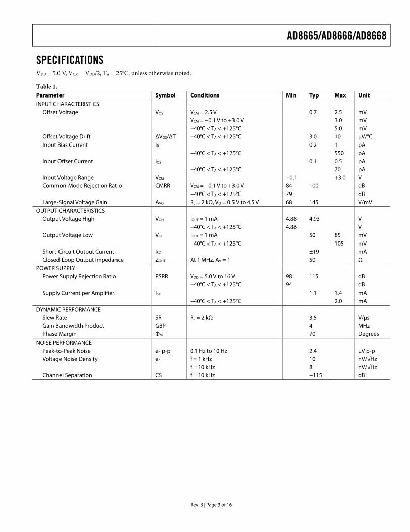
SPECIFICATIONS VDD = 5.0 V, VCM = VDD/2, TA = 25oC, unless otherwise noted.
Table 1. Parameter Symbol Conditions Min Typ Max Unit INPUT CHARACTERISTICS
Offset Voltage VOS VCM = 2.5 V 0.7 2.5 mV VCM = −0.1 V to +3.0 V 3.0 mV −40°C < TA < +125°C 5.0 mV Offset Voltage Drift ΔVOS/ΔT −40°C < TA < +125°C 3.0 10 μV/°C Input Bias Current IB 0.2 1 pA −40°C < TA < +125°C 550 pA Input Offset Current IOS 0.1 0.5 pA −40°C < TA < +125°C 70 pA Input Voltage Range VCM −0.1 +3.0 V Common-Mode Rejection Ratio CMRR VCM = −0.1 V to +3.0 V 84 100 dB −40°C < TA < +125°C 79 dB Large-Signal Voltage Gain AVO RL = 2 kΩ, VO = 0.5 V to 4.5 V 68 145 V/mV
OUTPUT CHARACTERISTICS Output Voltage High VOH IOUT = 1 mA 4.88 4.93 V −40°C < TA < +125°C 4.86 V Output Voltage Low VOL IOUT = 1 mA 50 85 mV −40°C < TA < +125°C 105 mV Short-Circuit Output Current ISC ±19 mA Closed-Loop Output Impedance ZOUT At 1 MHz, AV = 1 50 Ω
POWER SUPPLY Power Supply Rejection Ratio PSRR VDD = 5.0 V to 16 V 98 115 dB −40°C < TA < +125°C 94 dB Supply Current per Amplifier ISY 1.1 1.4 mA
−40°C < TA < +125°C 2.0 mA DYNAMIC PERFORMANCE
Slew Rate SR RL = 2 kΩ 3.5 V/μs Gain Bandwidth Product GBP 4 MHz Phase Margin ΦM 70 Degrees
NOISE PERFORMANCE Peak-to-Peak Noise en p-p 0.1 Hz to 10 Hz 2.4 μV p-p Voltage Noise Density en f = 1 kHz 10 nV/√Hz f = 10 kHz 8 nV/√Hz Channel Separation CS f = 10 kHz −115 dB
AD8665/AD8666/AD8668
Rev. B | Page 4 of 16
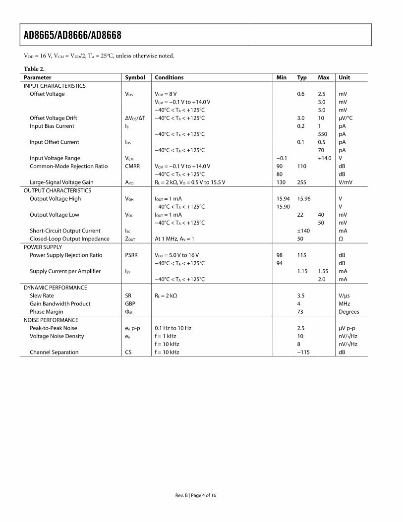
VDD = 16 V, VCM = VDD/2, TA = 25oC, unless otherwise noted.
Table 2. Parameter Symbol Conditions Min Typ Max Unit INPUT CHARACTERISTICS
Offset Voltage VOS VCM = 8 V 0.6 2.5 mV VCM = −0.1 V to +14.0 V 3.0 mV −40°C < TA < +125°C 5.0 mV Offset Voltage Drift ΔVOS/ΔT −40°C < TA < +125°C 3.0 10 μV/°C Input Bias Current IB 0.2 1 pA −40°C < TA < +125°C 550 pA Input Offset Current IOS 0.1 0.5 pA −40°C < TA < +125°C 70 pA Input Voltage Range VCM −0.1 +14.0 V Common-Mode Rejection Ratio CMRR VCM = −0.1 V to +14.0 V 90 110 dB −40°C < TA < +125°C 80 dB Large-Signal Voltage Gain AVO RL = 2 kΩ, VO = 0.5 V to 15.5 V 130 255 V/mV
OUTPUT CHARACTERISTICS Output Voltage High VOH IOUT = 1 mA 15.94 15.96 V −40°C < TA < +125°C 15.90 V Output Voltage Low VOL IOUT = 1 mA 22 40 mV −40°C < TA < +125°C 50 mV Short-Circuit Output Current ISC ±140 mA Closed-Loop Output Impedance ZOUT At 1 MHz, AV = 1 50 Ω
POWER SUPPLY Power Supply Rejection Ratio PSRR VDD = 5.0 V to 16 V 98 115 dB −40°C < TA < +125°C 94 dB Supply Current per Amplifier ISY 1.15 1.55 mA −40°C < TA < +125°C 2.0 mA
DYNAMIC PERFORMANCE Slew Rate SR RL = 2 kΩ 3.5 V/μs Gain Bandwidth Product GBP 4 MHz Phase Margin ΦM 73 Degrees
NOISE PERFORMANCE Peak-to-Peak Noise en p-p 0.1 Hz to 10 Hz 2.5 μV p-p Voltage Noise Density en f = 1 kHz 10 nV/√Hz f = 10 kHz 8 nV/√Hz Channel Separation CS f = 10 kHz −115 dB
AD8665/AD8666/AD8668
Rev. B | Page 5 of 16
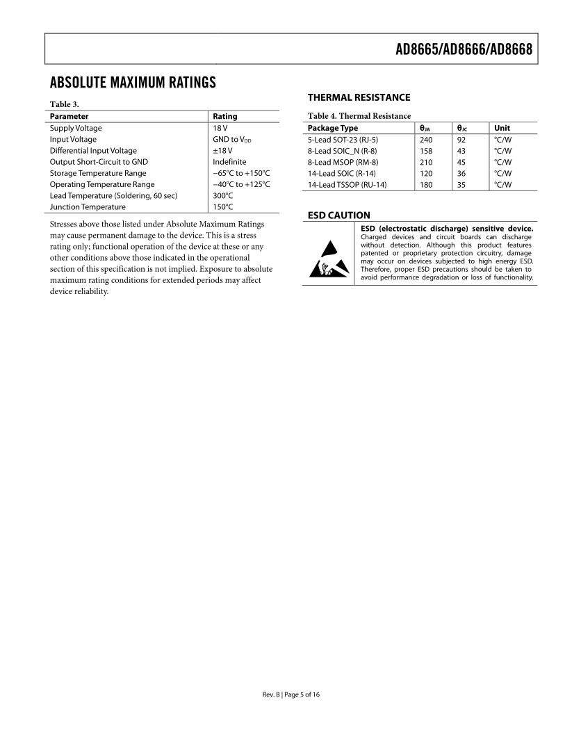
ABSOLUTE MAXIMUM RATINGS Table 3. Parameter Rating Supply Voltage 18 V Input Voltage GND to VDD
Differential Input Voltage ±18 V Output Short-Circuit to GND Indefinite Storage Temperature Range −65°C to +150°C Operating Temperature Range −40°C to +125°C Lead Temperature (Soldering, 60 sec) 300°C Junction Temperature 150°C
Stresses above those listed under Absolute Maximum Ratings may cause permanent damage to the device. This is a stress rating only; functional operation of the device at these or any other conditions above those indicated in the operational section of this specification is not implied. Exposure to absolute maximum rating conditions for extended periods may affect device reliability.
THERMAL RESISTANCE
Table 4. Thermal Resistance Package Type θJA θJC Unit 5-Lead SOT-23 (RJ-5) 240 92 °C/W 8-Lead SOIC_N (R-8) 158 43 °C/W 8-Lead MSOP (RM-8) 210 45 °C/W 14-Lead SOIC (R-14) 120 36 °C/W 14-Lead TSSOP (RU-14) 180 35 °C/W
ESD CAUTION
AD8665/AD8666/AD8668
Rev. B | Page 6 of 16
TYPICAL PERFORMANCE CHARACTERISTICS
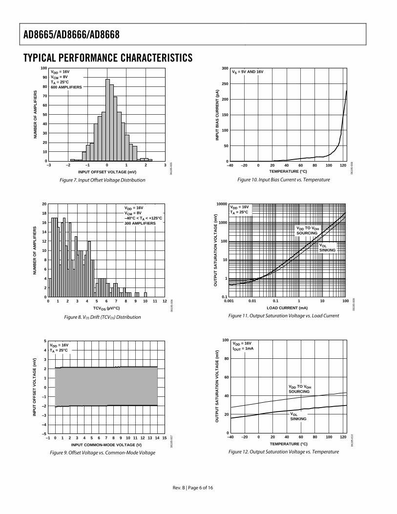
Figure 7. Input Offset Voltage Distribution
Figure 8. VOS Drift (TCVOS) Distribution
Figure 9. Offset Voltage vs. Common-Mode Voltage
Figure 10. Input Bias Current vs. Temperature
Figure 11. Output Saturation Voltage vs. Load Current
Figure 12. Output Saturation Voltage vs. Temperature
100
0–3 3
INPUT OFFSET VOLTAGE (mV)
NU
MB
ER O
F A
MPL
IFIE
RS
90
80
70
60
50
40
30
20
10
–2 –1 0 1 2
VDD = 16VVCM = 8VTA = 25°C600 AMPLIFIERS
0619
5-00
5
20
00 12
TCVOS (µV/°C)
NU
MB
ER O
F A
MPL
IFIE
RS
18
16
14
12
10
8
6
4
2
1 2 3 4 5 6 7 8 9 10 11
VDD = 16VVCM = 8V–40°C < TA < +125°C300 AMPLIFIERS
0619
5-00
6
5
–5–1 15
INPUT COMMON-MODE VOLTAGE (V)
INPU
T O
FFSE
T VO
LTA
GE
(mV)
4
3
2
1
0
–1
–2
–3
–4
0 1 2 3 4 5 6 7 8 9 10 11 12 13 14
VDD = 16VTA = 25°C
0619
5-00
7TEMPERATURE (°C)
INPU
T B
IAS
CU
RR
ENT
(pA
)
–400
300
250
200
150
100
50
1201008040 60200–20
VS = 5V AND 16V
0619
5-00
8
10000
0.10.001 100
LOAD CURRENT (mA)
OU
TPU
T SA
TUR
ATI
ON
VO
LTA
GE
(mV)
0.01 0.1 1 10
1
10
100
1000
VDD = 16VTA = 25°C
VDD TO VOHSOURCING
VOLSINKING
0619
5-00
9
100
0–40 120
TEMPERATURE (°C)
OU
TPU
T SA
TUR
ATI
ON
VO
LTA
GE
(mV)
80
60
40
20
–20 0 20 40 60 80 100
VDD = 16VIOUT = 1mA
VDD TO VOHSOURCING
VOLSINKING
0619
5-01
0
AD8665/AD8666/AD8668
Rev. B | Page 7 of 16
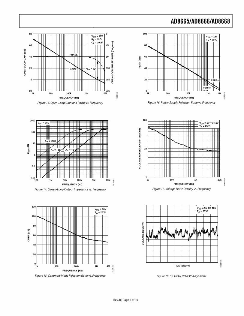
Figure 13. Open-Loop Gain and Phase vs. Frequency
Figure 14. Closed-Loop Output Impedance vs. Frequency
Figure 15. Common-Mode Rejection Ratio vs. Frequency
Figure 16. Power Supply Rejection Ratio vs. Frequency
Figure 17. Voltage Noise Density vs. Frequency
Figure 18. 0.1 Hz to 10 Hz Voltage Noise
80
–201k 10M
FREQUENCY (Hz)
OPE
N-L
OO
P G
AIN
(dB
)
10k 100k 1M
60
40
20
0
0
225
OPE
N-L
OO
P PH
ASE
SH
IFT
(Deg
rees
)
45
90
135
180
VDD = 16VRL = 2kΩCL = 10pF
ФM = 73°GAIN
PHASE
0619
5-01
1
1000
0.01100 10M
FREQUENCY (Hz)
Z OU
T (Ω
)
1k 10k 100k 1M
0.1
1
10
100
AV = +100
VDD = 16V
AV = +1
0619
5-01
2
AV = +10
120
01k 4M
FREQUENCY (Hz)
CM
RR
(dB
)
10k 100k 1M
100
80
60
40
20
VDD = 16VTA = 25°C
0619
5-01
3
100
01k 4M
FREQUENCY (Hz)
PSR
R (d
B)
10k 100k 1M
80
60
40
20
VDD = 16VTA = 25°C
PSRR–
PSRR+
0619
5-01
4
100
110 10k
FREQUENCY (Hz)
VOLT
AG
E N
OIS
E D
ENSI
TY (n
V/√H
z)
100 1k
10
VDD = 5V TO 16VTA = 25°C
0619
5-01
5
TIME (1s/DIV)
VOLT
AG
E (1
µV/D
IV)
VDD = 5V TO 16VTA = 25°C
0619
5-01
6
AD8665/AD8666/AD8668
Rev. B | Page 8 of 16
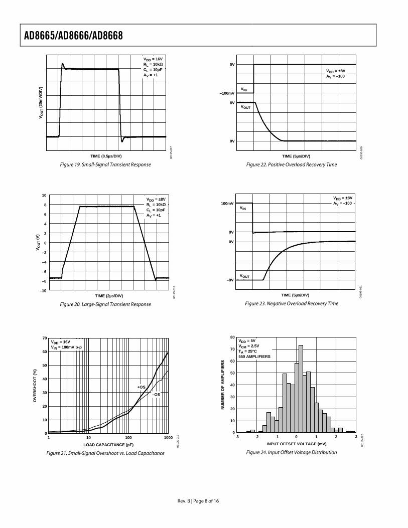
Figure 19. Small-Signal Transient Response
Figure 20. Large-Signal Transient Response
Figure 21. Small-Signal Overshoot vs. Load Capacitance
Figure 22. Positive Overload Recovery Time
Figure 23. Negative Overload Recovery Time
Figure 24. Input Offset Voltage Distribution
TIME (0.5µs/DIV)
V OU
T (2
0mV/
DIV
)
VDD = 16VRL = 10kΩCL = 10pFAV = +1
0619
5-01
7
TIME (2µs/DIV)
V OU
T (V
)
VDD = ±8VRL = 10kΩCL = 10pFAV = +1
10
–10
–8
–6
–4
–2
2
4
6
8
0
0619
5-01
8
70
01 1000
LOAD CAPACITANCE (pF)
OVE
RSH
OO
T (%
)
10 100
60
50
40
30
20
10
VDD = 16VVIN = 100mV p-p
+OS
–OS
0619
5-01
9
TIME (5µs/DIV)
0V
8V
–100mV
0V
VIN
VOUT
VDD = ±8VAV = –100
0619
5-02
0
TIME (5µs/DIV)
–8V
0V
0V
100mVVIN
VOUT
VDD = ±8VAV = –100
0619
5-02
1
80
0–3 3
INPUT OFFSET VOLTAGE (mV)
NU
MB
ER O
F A
MPL
IFIE
RS
70
60
50
40
30
20
10
–2 –1 0 1 2
VDD = 5VVCM = 2.5VTA = 25°C550 AMPLIFIERS
0619
5-02
2
AD8665/AD8666/AD8668
Rev. B | Page 9 of 16
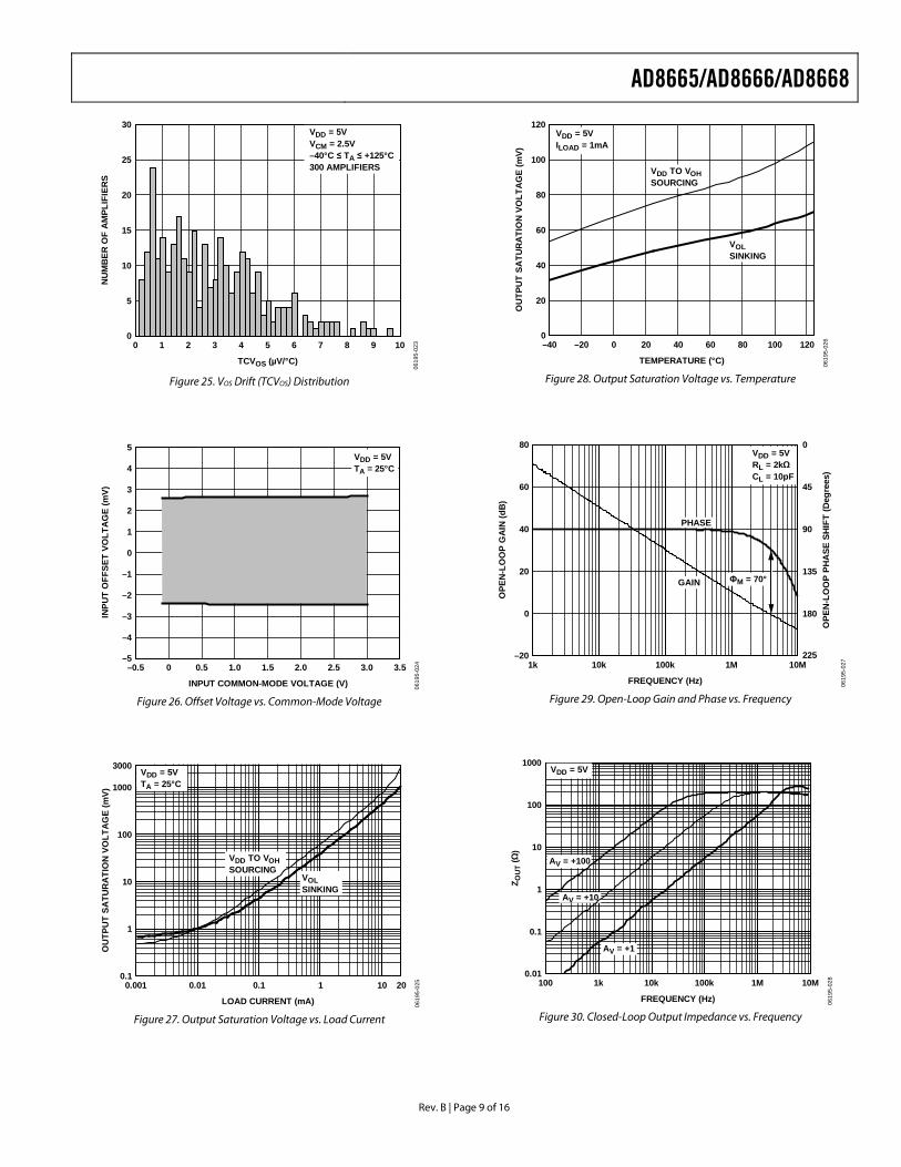
Figure 25. VOS Drift (TCVOS) Distribution
Figure 26. Offset Voltage vs. Common-Mode Voltage
Figure 27. Output Saturation Voltage vs. Load Current
Figure 28. Output Saturation Voltage vs. Temperature
Figure 29. Open-Loop Gain and Phase vs. Frequency
Figure 30. Closed-Loop Output Impedance vs. Frequency
30
00 10
TCVOS (µV/°C)
NU
MB
ER O
F A
MPL
IFIE
RS
25
20
15
10
5
1 2 3 4 5 6 7 8 9
VDD = 5VVCM = 2.5V–40°C ≤ TA ≤ +125°C300 AMPLIFIERS
0619
5-02
3
5
–5–0.5 3.5
INPUT COMMON-MODE VOLTAGE (V)
INPU
T O
FFSE
T VO
LTA
GE
(mV)
4
3
2
1
0
–1
–2
–3
–4
0 0.5 1.0 1.5 2.0 2.5 3.0
VDD = 5VTA = 25°C
0619
5-02
4
0.10.001
LOAD CURRENT (mA)
OU
TPU
T SA
TUR
ATI
ON
VO
LTA
GE
(mV)
0.01 0.1 1 10 20
1
10
100
1000
3000VDD = 5VTA = 25°C
VDD TO VOHSOURCING
VOLSINKING
0619
5-02
5
120
0–40 120
TEMPERATURE (°C)
OU
TPU
T SA
TUR
ATI
ON
VO
LTA
GE
(mV)
100
80
60
40
20
–20 0 20 40 60 80 100
VDD = 5VILOAD = 1mA
VDD TO VOHSOURCING
VOLSINKING
0619
5-02
6
80
–201k 10M
FREQUENCY (Hz)
OPE
N-L
OO
P G
AIN
(dB
)
10k 100k 1M
60
40
20
0
0
225
OPE
N-L
OO
P PH
ASE
SH
IFT
(Deg
rees
)
45
90
135
180
ФM = 70°GAIN
PHASE
VDD = 5VRL = 2kΩCL = 10pF
0619
5-02
7
1000
0.01100 10M
FREQUENCY (Hz)
Z OU
T (Ω)
1k 10k 100k 1M
0.1
1
10
100
VDD = 5V
AV = +100
AV = +10
AV = +1
0619
5-02
8
AD8665/AD8666/AD8668
Rev. B | Page 10 of 16
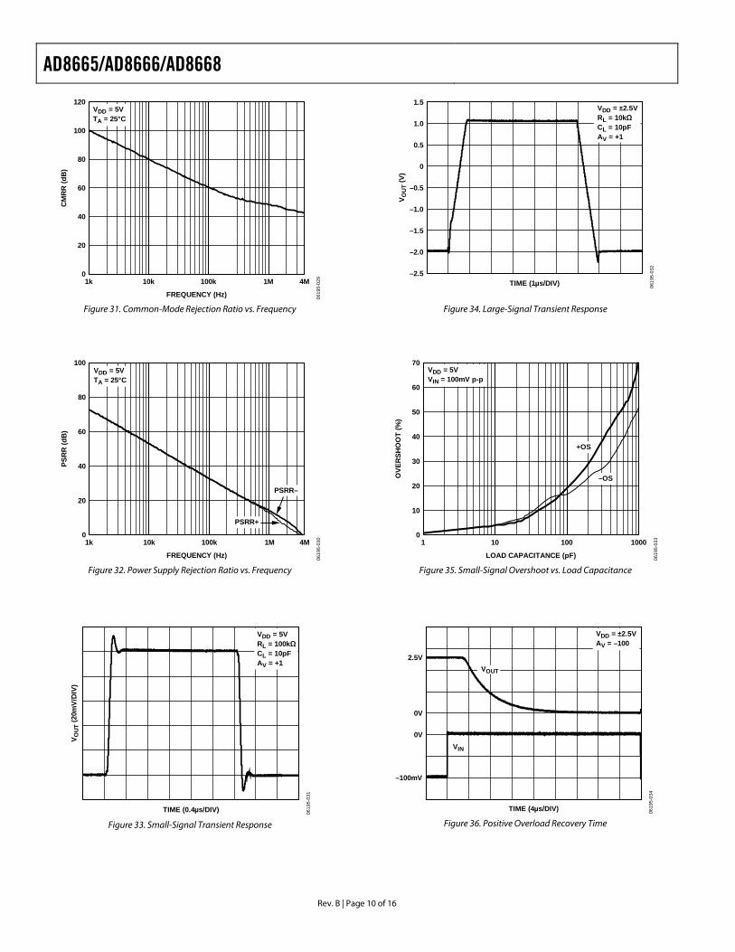
Figure 31. Common-Mode Rejection Ratio vs. Frequency
Figure 32. Power Supply Rejection Ratio vs. Frequency
Figure 33. Small-Signal Transient Response
Figure 34. Large-Signal Transient Response
Figure 35. Small-Signal Overshoot vs. Load Capacitance
Figure 36. Positive Overload Recovery Time
120
01k 4M
FREQUENCY (Hz)
CM
RR
(dB
)
10k 100k 1M
100
80
60
40
20
VDD = 5VTA = 25°C
0619
5-02
9
100
01k 4M
FREQUENCY (Hz)
PSR
R (d
B)
10k 100k 1M
80
60
40
20
VDD = 5VTA = 25°C
PSRR–
PSRR+
0619
5-03
0
TIME (0.4µs/DIV)
V OU
T (2
0mV/
DIV
)
VDD = 5VRL = 100kΩCL = 10pFAV = +1
0619
5-03
1
TIME (1µs/DIV)
V OU
T (V
)
1.5
–2.5
1.0
0.5
0
–0.5
–1.0
–1.5
–2.0
VDD = ±2.5VRL = 10kΩCL = 10pFAV = +1
0619
5-03
2
70
01 1000
LOAD CAPACITANCE (pF)
OVE
RSH
OO
T (%
)
10 100
60
50
40
30
20
10
VDD = 5VVIN = 100mV p-p
–OS
+OS
0619
5-03
3
TIME (4µs/DIV)
2.5V
0V
0V
–100mV
VDD = ±2.5VAV = –100
VOUT
VIN
0619
5-03
4
AD8665/AD8666/AD8668
Rev. B | Page 11 of 16
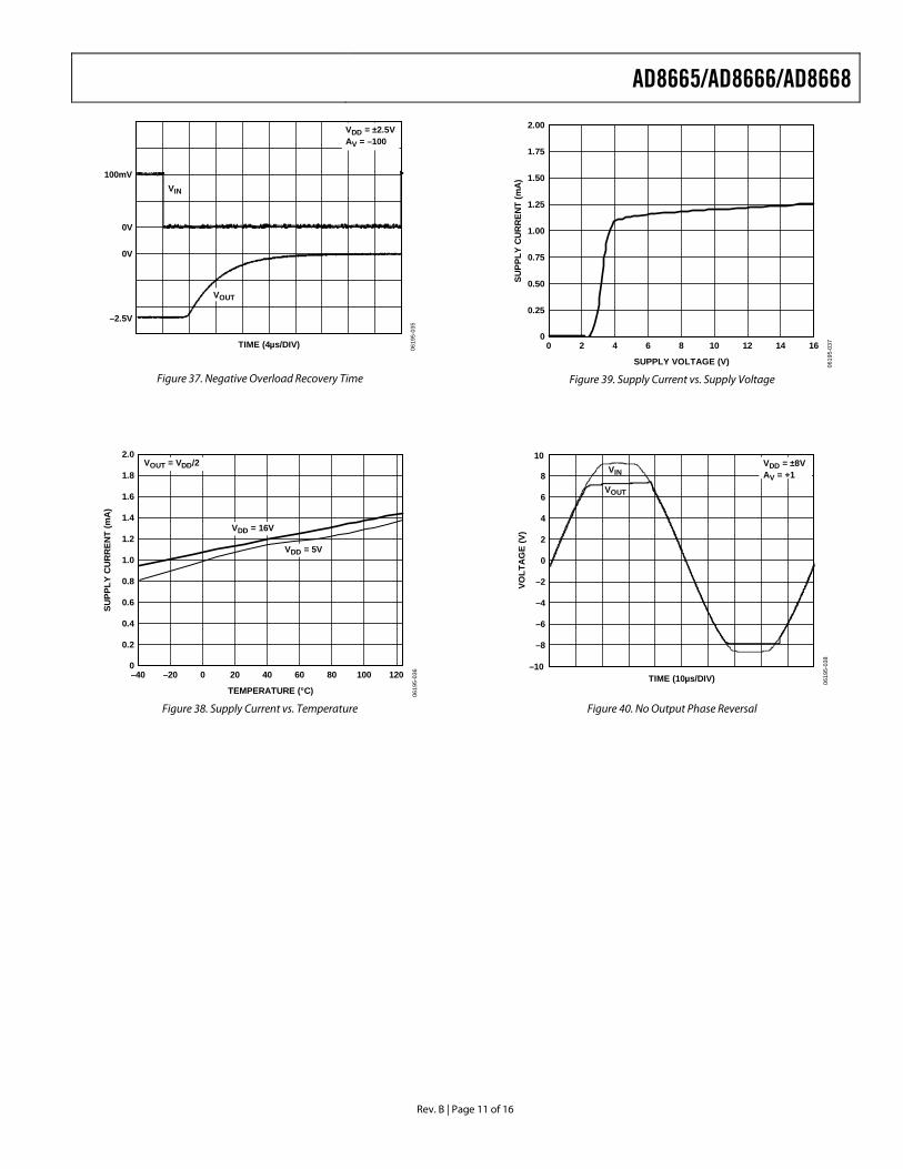
Figure 37. Negative Overload Recovery Time
Figure 38. Supply Current vs. Temperature
Figure 39. Supply Current vs. Supply Voltage
Figure 40. No Output Phase Reversal
TIME (4µs/DIV)
100mV
0V
0V
–2.5V
VDD = ±2.5VAV = –100
VOUT
VIN
0619
5-03
5
2.0
0–40 120
TEMPERATURE (°C)
SUPP
LY C
UR
REN
T (m
A)
1.8
1.6
1.4
1.2
1.0
0.8
0.6
0.4
0.2
–20 0 20 40 60 80 100
VOUT = VDD/2
VDD = 16V
VDD = 5V
0619
5-03
6
2.00
00 16
SUPPLY VOLTAGE (V)
SUPP
LY C
UR
REN
T (m
A)
1.75
1.50
1.25
1.00
0.75
0.50
0.25
2 4 6 8 10 12 14
0619
5-03
7
TIME (10µs/DIV)
VOLT
AG
E (V
)
VOUT
VIN
10
–10
8
6
4
2
0
–2
–4
–6
–8
VDD = ±8VAV = +1
0619
5-03
8
AD8665/AD8666/AD8668
Rev. B | Page 12 of 16
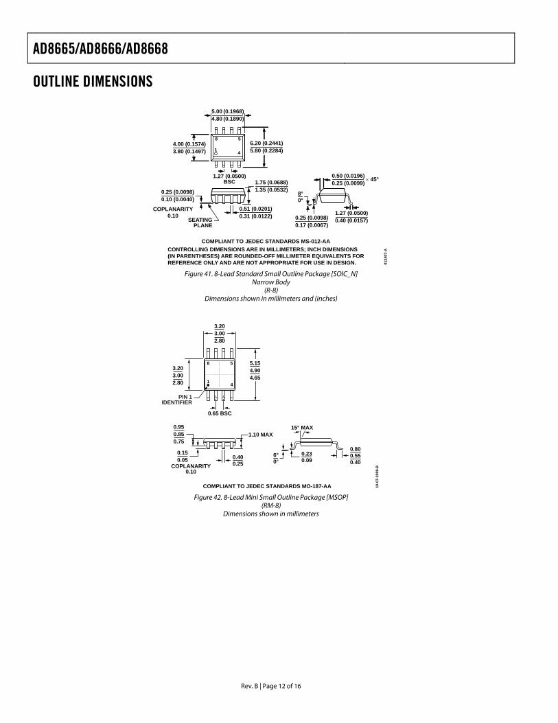
OUTLINE DIMENSIONS
Figure 41. 8-Lead Standard Small Outline Package [SOIC_N]
Narrow Body (R-8)
Dimensions shown in millimeters and (inches)
Figure 42. 8-Lead Mini Small Outline Package [MSOP]
(RM-8) Dimensions shown in millimeters
CONTROLLING DIMENSIONS ARE IN MILLIMETERS; INCH DIMENSIONS(IN PARENTHESES) ARE ROUNDED-OFF MILLIMETER EQUIVALENTS FORREFERENCE ONLY AND ARE NOT APPROPRIATE FOR USE IN DESIGN.
COMPLIANT TO JEDEC STANDARDS MS-012-AA
0124
07-A
0.25 (0.0098)0.17 (0.0067)
1.27 (0.0500)0.40 (0.0157)
0.50 (0.0196)0.25 (0.0099) 45°
8°0°
1.75 (0.0688)1.35 (0.0532)
SEATINGPLANE
0.25 (0.0098)0.10 (0.0040)
41
8 5
5.00 (0.1968)4.80 (0.1890)
4.00 (0.1574)3.80 (0.1497)
1.27 (0.0500)BSC
6.20 (0.2441)5.80 (0.2284)
0.51 (0.0201)0.31 (0.0122)
COPLANARITY0.10
COMPLIANT TO JEDEC STANDARDS MO-187-AA
6°0°
0.800.550.40
4
8
1
5
0.65 BSC
0.400.25
1.10 MAX
3.203.002.80
COPLANARITY0.10
0.230.09
3.203.002.80
5.154.904.65
PIN 1IDENTIFIER
15° MAX0.950.850.75
0.150.05
10-0
7-20
09-B
AD8665/AD8666/AD8668
Rev. B | Page 13 of 16
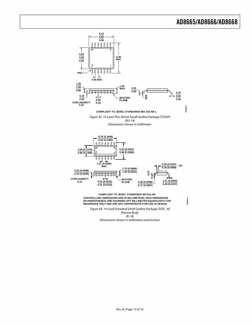
Figure 43. 14-Lead Thin Shrink Small Outline Package [TSSOP]
(RU-14) Dimensions shown in millimeters
Figure 44. 14-Lead Standard Small Outline Package [SOIC_N]
Narrow Body (R-14)
Dimensions shown in millimeters and (inches)
COMPLIANT TO JEDEC STANDARDS MO-153-AB-1 0619
08-A
8°0°
4.504.404.30
14 8
71
6.40BSC
PIN 1
5.105.004.90
0.65 BSC
0.150.05 0.30
0.19
1.20MAX
1.051.000.80
0.200.09 0.75
0.600.45
COPLANARITY0.10
SEATINGPLANE
CONTROLLING DIMENSIONS ARE IN MILLIMETERS; INCH DIMENSIONS(IN PARENTHESES) ARE ROUNDED-OFF MILLIMETER EQUIVALENTS FORREFERENCE ONLY AND ARE NOT APPROPRIATE FOR USE IN DESIGN.
COMPLIANT TO JEDEC STANDARDS MS-012-AB
0606
06-A
14 8
71
6.20 (0.2441)5.80 (0.2283)
4.00 (0.1575)3.80 (0.1496)
8.75 (0.3445)8.55 (0.3366)
1.27 (0.0500)BSC
SEATINGPLANE
0.25 (0.0098)0.10 (0.0039)
0.51 (0.0201)0.31 (0.0122)
1.75 (0.0689)1.35 (0.0531)
0.50 (0.0197)0.25 (0.0098)
1.27 (0.0500)0.40 (0.0157)
0.25 (0.0098)0.17 (0.0067)
COPLANARITY0.10
8°0°
45°
AD8665/AD8666/AD8668
Rev. B | Page 14 of 16
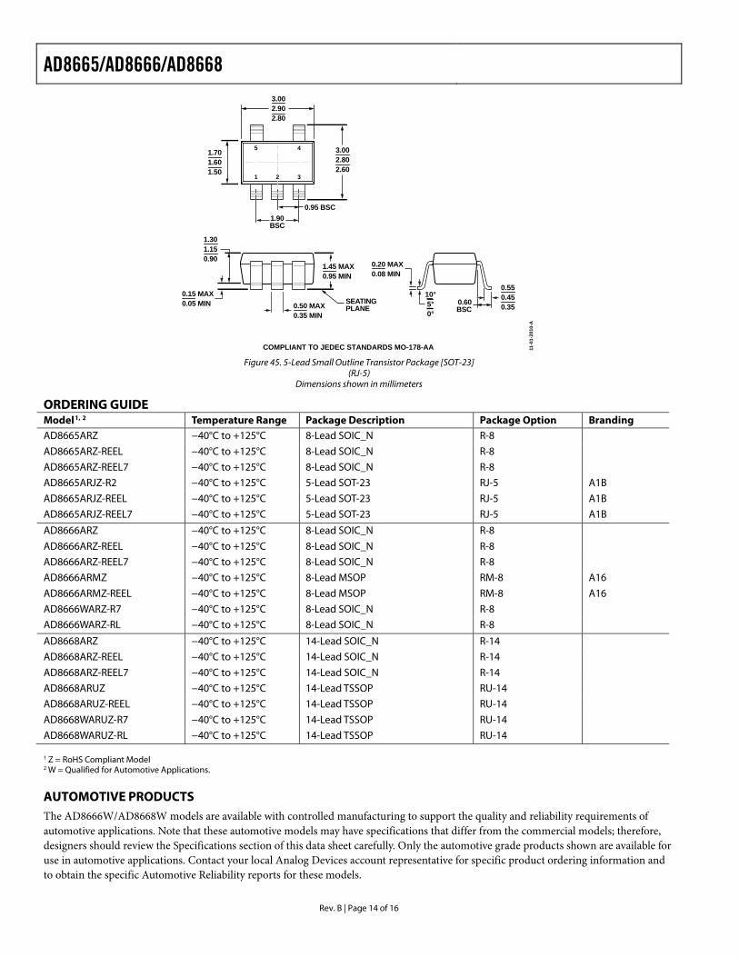
Figure 45. 5-Lead Small Outline Transistor Package [SOT-23]
(RJ-5) Dimensions shown in millimeters
ORDERING GUIDE Model1, 2 Temperature Range Package Description Package Option Branding AD8665ARZ −40°C to +125°C 8-Lead SOIC_N R-8
AD8665ARZ-REEL −40°C to +125°C 8-Lead SOIC_N R-8
AD8665ARZ-REEL7 −40°C to +125°C 8-Lead SOIC_N R-8
AD8665ARJZ-R2 −40°C to +125°C 5-Lead SOT-23 RJ-5 A1B
AD8665ARJZ-REEL −40°C to +125°C 5-Lead SOT-23 RJ-5 A1B
AD8665ARJZ-REEL7 −40°C to +125°C 5-Lead SOT-23 RJ-5 A1B
AD8666ARZ −40°C to +125°C 8-Lead SOIC_N R-8
AD8666ARZ-REEL −40°C to +125°C 8-Lead SOIC_N R-8
AD8666ARZ-REEL7 −40°C to +125°C 8-Lead SOIC_N R-8
AD8666ARMZ −40°C to +125°C 8-Lead MSOP RM-8 A16
AD8666ARMZ-REEL −40°C to +125°C 8-Lead MSOP RM-8 A16
AD8666WARZ-R7 −40°C to +125°C 8-Lead SOIC_N R-8
AD8666WARZ-RL −40°C to +125°C 8-Lead SOIC_N R-8
AD8668ARZ −40°C to +125°C 14-Lead SOIC_N R-14
AD8668ARZ-REEL −40°C to +125°C 14-Lead SOIC_N R-14
AD8668ARZ-REEL7 −40°C to +125°C 14-Lead SOIC_N R-14
AD8668ARUZ −40°C to +125°C 14-Lead TSSOP RU-14
AD8668ARUZ-REEL −40°C to +125°C 14-Lead TSSOP RU-14
AD8668WARUZ-R7 −40°C to +125°C 14-Lead TSSOP RU-14
AD8668WARUZ-RL −40°C to +125°C 14-Lead TSSOP RU-14 1 Z = RoHS Compliant Model 2 W = Qualified for Automotive Applications.
AUTOMOTIVE PRODUCTS The AD8666W/AD8668W models are available with controlled manufacturing to support the quality and reliability requirements of automotive applications. Note that these automotive models may have specifications that differ from the commercial models; therefore, designers should review the Specifications section of this data sheet carefully. Only the automotive grade products shown are available for use in automotive applications. Contact your local Analog Devices account representative for specific product ordering information and to obtain the specific Automotive Reliability reports for these models.
COMPLIANT TO JEDEC STANDARDS MO-178-AA
10°5°0°
SEATINGPLANE
1.90BSC
0.95 BSC
0.60BSC
5
1 2 3
4
3.002.902.80
3.002.802.60
1.701.601.50
1.301.150.90
0.15 MAX0.05 MIN
1.45 MAX0.95 MIN
0.20 MAX0.08 MIN
0.50 MAX0.35 MIN
0.550.450.35
11-0
1-20
10-A

AD8665/AD8666/AD8668
Rev. B | Page 15 of 16
NOTES
AD8665/AD8666/AD8668
Rev. B | Page 16 of 16
NOTES
©2006–2011 Analog Devices, Inc. All rights reserved. Trademarks and registered trademarks are the property of their respective owners. D06195-0-7/11(B)