Embed Size (px)
Citation preview
16-Bit, 8-Channel Serial Output SamplingANALOG-TO-DIGITAL CONVERTER
FEATURES PIN FOR PIN WITH ADS7844
SINGLE SUPPLY: 2.7V to 5V
8-CHANNEL SINGLE-ENDED OR4-CHANNEL DIFFERENTIAL INPUT
UP TO 100kHz CONVERSION RATE
84dB SINAD
SERIAL INTERFACE
QSOP-20 AND SSOP-20 PACKAGES
APPLICATIONS DATA ACQUISITION
TEST AND MEASUREMENT EQUIPMENT
INDUSTRIAL PROCESS CONTROL
PERSONAL DIGITAL ASSISTANTS
BATTERY-POWERED SYSTEMS
DESCRIPTIONThe ADS8344 is an 8-channel, 16-bit, samplingAnalog-to-Digital (A/D) converter with a synchronous serialinterface. Typical power dissipation is 10mW at a 100kHzthroughput rate and a +5V supply. The reference voltage(VREF) can be varied between 500mV and VCC, providing acorresponding input voltage range of 0V to VREF. Thedevice includes a shutdown mode that reduces power dissi-pation to under 15µW. The ADS8344 is tested down to 2.7Voperation.
Low power, high speed, and an on-board multiplexer makethe ADS8344 ideal for battery-operated systems such aspersonal digital assistants, portable multi-channel data log-gers, and measurement equipment. The serial interface alsoprovides low-cost isolation for remote data acquisition. TheADS8344 is available in a QSOP-20 or SSOP-20 packageand is ensured over the –40°C to +85°C temperature range.
CDAC
SAR
Comparator
8-ChannelMultiplexer
SerialInterface
andControl
CH4
CH5
CH6
CH7
COM
VREF
CS
SHDN
DIN
DOUT
BUSY
DCLK
CH0
CH1
CH2
CH3
4-ChannelMultiplexer
CH0
CH1
CH2
CH3
COM
ADS8343ADS8341
ADS8345ADS8344
¤ADS8344
¤ADS8344
ADS8344
SBAS139E – SEPTEMBER 2000 – REVISED SEPTEMBER 2006
www.ti.com
PRODUCTION DATA information is current as of publication date.Products conform to specifications per the terms of Texas Instrumentsstandard warranty. Production processing does not necessarily includetesting of all parameters.
Copyright © 2000-2006, Texas Instruments Incorporated
Please be aware that an important notice concerning availability, standard warranty, and use in critical applications ofTexas Instruments semiconductor products and disclaimers thereto appears at the end of this data sheet.
All trademarks are the property of their respective owners.
ADS83442SBAS139E
MINIMUMRELATIVE MAXIMUM SPECIFIED PACKAGE
ACCURACY GAIN ERROR TEMPERATURE PACKAGE DRAWING ORDERING TRANSPORTPRODUCT (LSB) (%) RANGE DESIGNATOR PACKAGE-LEAD NUMBER NUMBER MEDIA, QUANTITY
ADS8344E 8 ±0.05 –40°C to +85°C DBQ QSOP-20 DBQ ADS8344E Rails, 56" " " " " " " ADS8344E/2K5 Tape and Reel, 2500
ADS8344N " " " DB SSOP-20 DB ADS8344N Rails, 68" " " " " " " ADS8344N/1K Tape and Reel, 1000
ADS8344EB 6 ±0.024 –40°C to +85°C DBQ QSOP-20 DBQ ADS8344EB Rails, 56" " " " " " " ADS8344EB/2K5 Tape and Reel, 2500
ADS8344NB " " " DB SSOP-20 DB ADS8344NB Rails, 68" " " " " " " ADS8344NB/1K Tape and Reel, 1000
NOTE: (1) For the most current package and ordering information, see the Package Option Addendum at the end of this data sheet, or see the TI web site atwww.ti.com.
PACKAGE/ORDERING INFORMATION(1)
ABSOLUTE MAXIMUM RATINGS(1)
+VCC to GND ........................................................................ –0.3V to +6VAnalog Inputs to GND ............................................ –0.3V to +VCC + 0.3V
Digital Inputs to GND ........................................................... –0.3V to +6V
Power Dissipation .......................................................................... 250mW
Maximum Junction Temperature ................................................... +150°COperating Temperature Range ........................................ –40°C to +85°CStorage Temperature Range ......................................... –65°C to +150°CLead Temperature (soldering, 10s) ............................................... +300°C
NOTE: (1) Stresses above those listed under Absolute Maximum Ratings maycause permanent damage to the device. Exposure to absolute maximumconditions for extended periods may affect device reliability.
PIN CONFIGURATION
Top View SSOP
PIN DESCRIPTIONS
PIN NAME DESCRIPTION
1 CH0 Analog Input Channel 02 CH1 Analog Input Channel 13 CH2 Analog Input Channel 24 CH3 Analog Input Channel 35 CH4 Analog Input Channel 46 CH5 Analog Input Channel 57 CH6 Analog Input Channel 68 CH7 Analog Input Channel 79 COM Ground reference for analog inputs. Sets zero code
voltage in single–ended mode. Connect this pin to groundor ground reference point.
10 SHDN Shutdown. When LOW, the device enters a verylow-power shutdown mode.
11 VREF Voltage Reference Input. See Electrical CharacteristicsTable for ranges.
12 +VCC Power Supply, 2.7V to 5V13 GND Ground14 GND Ground15 DOUT Serial Data Output. Data is shifted on the falling edge of
DCLK. This output is high impedance when CS is HIGH.16 BUSY Busy Output. Busy goes LOW when the DIN control bits
are being read and also when the device is converting.The Output is high impedance when CS is HIGH.
17 DIN Serial Data Input. If CS is LOW, data is latched on risingedge of DCLK.
18 CS Chip Select Input. Active LOW. Data will not be clockedinto DIN unless CS is LOW. When CS is HIGH, DOUT ishigh impedance.
19 DCLK External Clock Input. The clock speed determines theconversion rate by the equation fDCLK = 24 • fSAMPLE.
20 +VCC Power Supply
1
2
3
4
5
6
7
8
9
10
CH0
CH1
CH2
CH3
CH4
CH5
CH6
CH7
COM
SHDN
+VCC
DCLK
CS
DIN
BUSY
DOUT
GND
GND
+VCC
VREF
20
19
18
17
16
15
14
13
12
11
ADS8344
ELECTROSTATICDISCHARGE SENSITIVITY
This integrated circuit can be damaged by ESD. Texas Instrumentsrecommends that all integrated circuits be handled with appropriateprecautions. Failure to observe proper handling and installation proce-dures can cause damage.
ESD damage can range from subtle performance degradation tocomplete device failure. Precision integrated circuits may be moresusceptible to damage because very small parametric changes couldcause the device not to meet its published specifications.
ADS8344 3SBAS139E
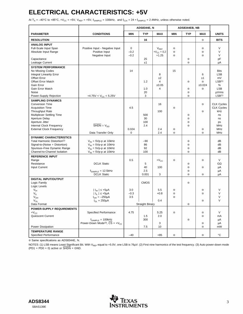
ELECTRICAL CHARACTERISTICS: +5VAt TA = –40°C to +85°C, +VCC = +5V, VREF = +5V, fSAMPLE = 100kHz, and fCLK = 24 • fSAMPLE = 2.4MHz, unless otherwise noted.
ADS8344E, N ADS8344EB, NB
PARAMETER CONDITIONS MIN TYP MAX MIN TYP MAX UNITS
RESOLUTION 16 BITS
ANALOG INPUTFull-Scale Input Span Positive Input - Negative Input 0 VREF VAbsolute Input Range Positive Input –0.2 +VCC + 0.2 V
Negative Input –0.2 +1.25 VCapacitance 25 pFLeakage Current ±1 µA
SYSTEM PERFORMANCENo Missing Codes 14 15 BitsIntegral Linearity Error 8 6 LSBOffset Error ±2 ±1 mVOffset Error Match 1.2 4 LSB(1)
Gain Error ±0.05 ±0.024 %Gain Error Match 1.0 4 LSBNoise 20 µVrmsPower-Supply Rejection +4.75V < VCC < 5.25V 3 LSB(1)
SAMPLING DYNAMICSConversion Time 16 CLK CyclesAcquisition Time 4.5 CLK CyclesThroughput Rate 100 kHzMultiplexer Settling Time 500 nsAperture Delay 30 nsAperture Jitter 100 psInternal Clock Frequency SHDN = VDD 2.4 MHzExternal Clock Frequency 0.024 2.4 MHz
Data Transfer Only 0 2.4 MHz
DYNAMIC CHARACTERISTICSTotal Harmonic Distortion(2) VIN = 5Vp-p at 10kHz –90 dBSignal-to-(Noise + Distortion) VIN = 5Vp-p at 10kHz 86 dBSpurious–Free Dynamic Range VIN = 5Vp-p at 10kHz 92 dBChannel-to-Channel Isolation VIN = 5Vp-p at 10kHz 100 dB
REFERENCE INPUTRange 0.5 +VCC VResistance DCLK Static 5 GΩInput Current 40 100 µA
fSAMPLE = 12.5kHz 2.5 µADCLK Static 0.001 3 µA
DIGITAL INPUT/OUTPUTLogic Family CMOS
Logic LevelsVIH | IIH | ≤ +5µA 3.0 5.5 VVIL | IIL | ≤ +5µA –0.3 +0.8 VVOH IOH = –250µA 3.5 VVOL IOL = 250µA 0.4 V
Data Format Straight Binary
POWER-SUPPLY REQUIREMENTS+VCC Specified Performance 4.75 5.25 VQuiescent Current 1.5 2.0 mA
fSAMPLE = 100kHz 300 µAPower-Down Mode(3), CS = +VCC 3 µA
Power Dissipation 7.5 10 mW
TEMPERATURE RANGESpecified Performance –40 +85 °C
Same specifications as ADS8344E, N.
NOTES: (1) LSB means Least Significant Bit. With VREF equal to +5.0V, one LSB is 76µV. (2) First nine harmonics of the test frequency. (3) Auto power-down mode(PD1 = PD0 = 0) active or SHDN = GND.
ADS83444SBAS139E
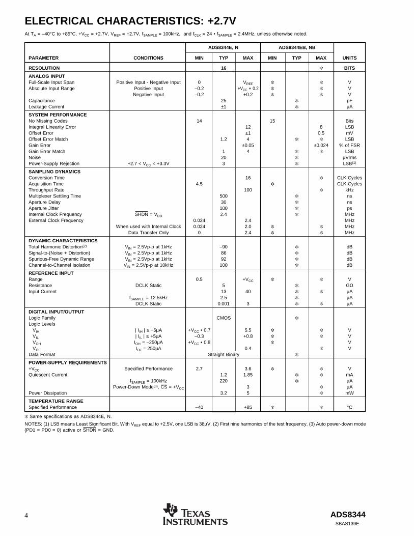
ELECTRICAL CHARACTERISTICS: +2.7VAt TA = –40°C to +85°C, +VCC = +2.7V, VREF = +2.7V, fSAMPLE = 100kHz, and fCLK = 24 • fSAMPLE = 2.4MHz, unless otherwise noted.
ADS8344E, N ADS8344EB, NB
Same specifications as ADS8344E, N.
NOTES: (1) LSB means Least Significant Bit. With VREF equal to +2.5V, one LSB is 38µV. (2) First nine harmonics of the test frequency. (3) Auto power-down mode(PD1 = PD0 = 0) active or SHDN = GND.
PARAMETER CONDITIONS MIN TYP MAX MIN TYP MAX UNITS
RESOLUTION 16 BITS
ANALOG INPUTFull-Scale Input Span Positive Input - Negative Input 0 VREF VAbsolute Input Range Positive Input –0.2 +VCC + 0.2 V
Negative Input –0.2 +0.2 VCapacitance 25 pFLeakage Current ±1 µA
SYSTEM PERFORMANCENo Missing Codes 14 15 BitsIntegral Linearity Error 12 8 LSBOffset Error ±1 0.5 mVOffset Error Match 1.2 4 LSBGain Error ±0.05 ±0.024 % of FSRGain Error Match 1 4 LSBNoise 20 µVrmsPower-Supply Rejection +2.7 < VCC < +3.3V 3 LSB(1)
SAMPLING DYNAMICSConversion Time 16 CLK CyclesAcquisition Time 4.5 CLK CyclesThroughput Rate 100 kHzMultiplexer Settling Time 500 nsAperture Delay 30 nsAperture Jitter 100 psInternal Clock Frequency SHDN = VDD 2.4 MHzExternal Clock Frequency 0.024 2.4 MHz
When used with Internal Clock 0.024 2.0 MHzData Transfer Only 0 2.4 MHz
DYNAMIC CHARACTERISTICSTotal Harmonic Distortion(2) VIN = 2.5Vp-p at 1kHz –90 dBSignal-to-(Noise + Distortion) VIN = 2.5Vp-p at 1kHz 86 dBSpurious-Free Dynamic Range VIN = 2.5Vp-p at 1kHz 92 dBChannel-to-Channel Isolation VIN = 2.5Vp-p at 10kHz 100 dB
REFERENCE INPUTRange 0.5 +VCC VResistance DCLK Static 5 GΩInput Current 13 40 µA
fSAMPLE = 12.5kHz 2.5 µADCLK Static 0.001 3 µA
DIGITAL INPUT/OUTPUTLogic Family CMOS
Logic LevelsVIH | IIH | ≤ +5µA +VCC • 0.7 5.5 VVIL | IIL | ≤ +5µA –0.3 +0.8 VVOH IOH = –250µA +VCC • 0.8 VVOL IOL = 250µA 0.4 V
Data Format Straight Binary
POWER-SUPPLY REQUIREMENTS+VCC Specified Performance 2.7 3.6 VQuiescent Current 1.2 1.85 mA
fSAMPLE = 100kHz 220 µAPower-Down Mode(3), CS = +VCC 3 µA
Power Dissipation 3.2 5 mW
TEMPERATURE RANGESpecified Performance –40 +85 °C
ADS8344 5SBAS139E
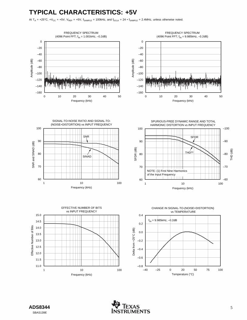
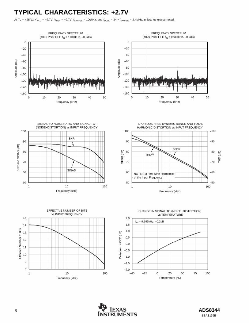
TYPICAL CHARACTERISTICS: +5VAt TA = +25°C, +VCC = +5V, VREF = +5V, fSAMPLE = 100kHz, and fDCLK = 24 • fSAMPLE = 2.4MHz, unless otherwise noted.
0
–20
–40
–60
–80
–100
–120
–140
–160
FREQUENCY SPECTRUM(4096 Point FFT; fIN = 1.001kHz, –0.2dB)
0 10 20 30 40 50
Frequency (kHz)
Am
plitu
de (
dB)
0
–20
–40
–60
–80
–100
–120
–140
–160
FREQUENCY SPECTRUM(4096 Point FFT; fIN = 9.985kHz, –0.2dB)
0 10 20 30 40 50
Frequency (kHz)
Am
plitu
de (
dB)
SIGNAL-TO-NOISE RATIO AND SIGNAL-TO-(NOISE+DISTORTION) vs INPUT FREQUENCY
101 100
Frequency (kHz)
SN
R a
nd S
INA
D (
dB)
100
90
80
70
60
SINAD
SNR
SPURIOUS-FREE DYNAMIC RANGE AND TOTALHARMONIC DISTORTION vs INPUT FREQUENCY
101 100
Frequency (kHz)
SF
DR
(dB
)
TH
D (
dB)
100
90
80
70
60
–100
–90
–80
–70
–60
THD(1)
SFDR
NOTE: (1) First Nine Harmonicsof the Input Frequency
CHANGE IN SIGNAL-TO-(NOISE+DISTORTION) vs TEMPERATURE
–40 –25 0 20 50 75 100
Temperature (°C)
Del
ta fr
om +
25°C
(dB
)
0.2
0.0
–0.2
–0.4
–0.6
–0.8
0.4
fIN = 9.985kHz, –0.2dB
EFFECTIVE NUMBER OF BITSvs INPUT FREQUENCY
101 100
Frequency (kHz)
Effe
ctiv
e N
umbe
r of
Bits
15.0
14.5
14.0
13.5
13.0
12.5
12.0
11.5
11.0
ADS83446SBAS139E
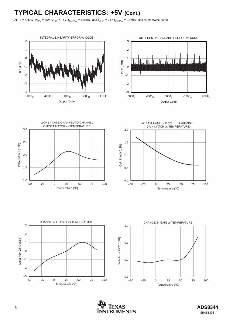
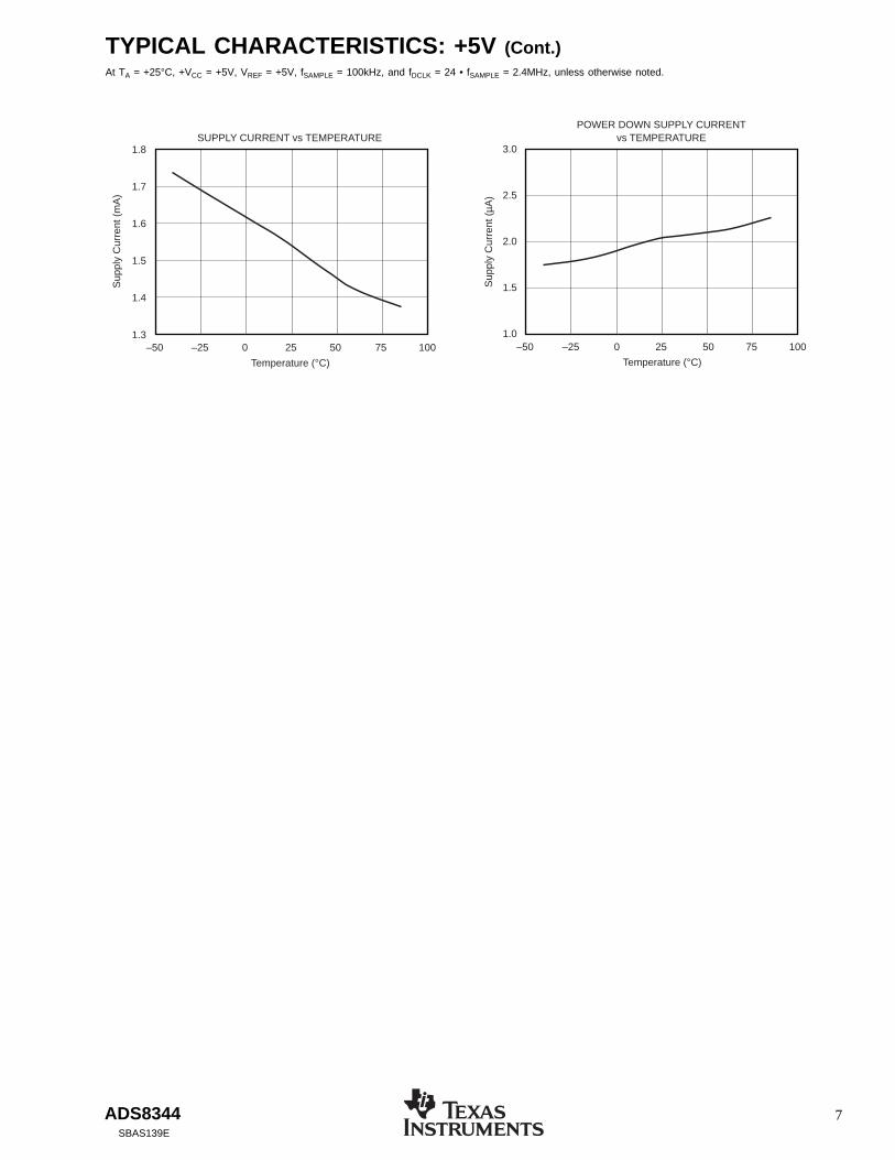
TYPICAL CHARACTERISTICS: +5V (Cont.)At TA = +25°C, +VCC = +5V, VREF = +5V, fSAMPLE = 100kHz, and fDCLK = 24 • fSAMPLE = 2.4MHz, unless otherwise noted.
Output Code
2
1
0
–1
–2
–3
–4
INTEGRAL LINEARITY ERROR vs CODE
8000H C000H FFFFH0000H 4000H
ILE
(LS
B)
Output Code
3
2
1
0
–1
–2
–3
DIFFERENTIAL LINEARITY ERROR vs CODE
8000H C000H FFFFH0000H 4000H
DLE
(LS
B)
WORST CASE CHANNEL-TO-CHANNELOFFSET MATCH vs TEMPERATURE
3.0
2.5
2.0
1.5
1.0
Offs
et M
atch
(LS
B)
Temperature (°C)
–50 –25 0 25 50 75 100
WORST CASE CHANNEL-TO-CHANNELGAIN MATCH vs TEMPERATURE
2.0
1.5
1.0
0.5
0.0
Gai
n M
atch
(LS
B)
Temperature (°C)
–50 –25 0 25 50 75 100
3
2
1
0
–1
–2
–3–50 –25 0 25 50 75 100
CHANGE IN OFFSET vs TEMPERATURE
Temperature (°C)
Del
ta fr
om 2
5°C
(LS
B)
1.0
0.5
0.0
–0.5–50 –25 0 25 50 75 100
CHANGE IN GAIN vs TEMPERATURE
Temperature (°C)
Del
ta fr
om 2
5°C
(LS
B)
ADS8344 7SBAS139E
1.8
1.7
1.6
1.5
1.4
1.3–50 –25 0 25 50 75 100
SUPPLY CURRENT vs TEMPERATURE
Temperature (°C)
Sup
ply
Cur
rent
(m
A)
TYPICAL CHARACTERISTICS: +5V (Cont.)At TA = +25°C, +VCC = +5V, VREF = +5V, fSAMPLE = 100kHz, and fDCLK = 24 • fSAMPLE = 2.4MHz, unless otherwise noted.
POWER DOWN SUPPLY CURRENTvs TEMPERATURE
3.0
2.5
2.0
1.5
1.0
Sup
ply
Cur
rent
(µA
)
Temperature (°C)
–50 –25 0 25 50 75 100
ADS83448SBAS139E
TYPICAL CHARACTERISTICS: +2.7VAt TA = +25°C, +VCC = +2.7V, VREF = +2.7V, fSAMPLE = 100kHz, and fDCLK = 24 • fSAMPLE = 2.4MHz, unless otherwise noted.
0
–20
–40
–60
–80
–100
–120
–140
–160
FREQUENCY SPECTRUM(4096 Point FFT; fIN = 1.001kHz, –0.2dB)
0 10 20 30 40 50
Frequency (kHz)
Am
plitu
de (
dB)
0
–20
–40
–60
–80
–100
–120
–140
–160
FREQUENCY SPECTRUM(4096 Point FFT; fIN = 9.985kHz, –0.2dB)
0 10 20 30 40 50
Frequency (kHz)
Am
plitu
de (
dB)
SIGNAL-TO-NOISE RATIO AND SIGNAL-TO-(NOISE+DISTORTION) vs INPUT FREQUENCY
101 100
Frequency (kHz)
SN
R a
nd S
INA
D (
dB)
100
90
80
70
60
50
SINAD
SNR
SPURIOUS-FREE DYNAMIC RANGE AND TOTALHARMONIC DISTORTION vs INPUT FREQUENCY
101 100
Frequency (kHz)
SF
DR
(dB
)
THD(1)
SFDR
100
90
80
70
60
50
TH
D (
dB)
–100
–90
–80
–70
–60
–50
NOTE: (1) First Nine Harmonicsof the Input Frequency
EFFECTIVE NUMBER OF BITSvs INPUT FREQUENCY
101 100
Frequency (kHz)
Effe
ctiv
e N
umbe
r of
Bits
15
14
13
12
11
10
9
8
CHANGE IN SIGNAL-TO-(NOISE+DISTORTION) vs TEMPERATURE
–40 –25 0 20 50 75 100
Temperature (°C)
Del
ta fr
om +
25°C
(dB
)
2.0
1.5
1.0
0.5
0.0
–0.5
–1.0
–1.5
–2.0
fIN = 9.985kHz, –0.2dB
ADS8344 9SBAS139E
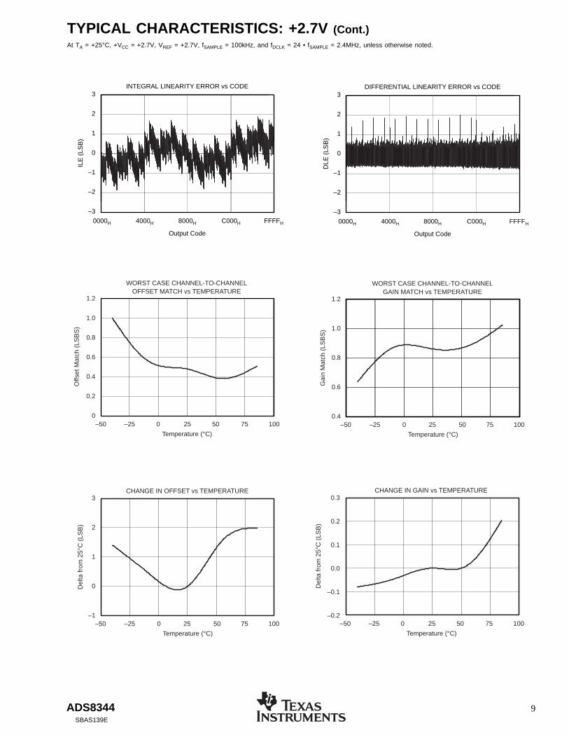
TYPICAL CHARACTERISTICS: +2.7V (Cont.)At TA = +25°C, +VCC = +2.7V, VREF = +2.7V, fSAMPLE = 100kHz, and fDCLK = 24 • fSAMPLE = 2.4MHz, unless otherwise noted.
Output Code
3
2
1
0
–1
–2
–3
INTEGRAL LINEARITY ERROR vs CODE
8000H C000H FFFFH0000H 4000H
ILE
(LS
B)
Output Code
3
2
1
0
–1
–2
–3
DIFFERENTIAL LINEARITY ERROR vs CODE
8000H C000H FFFFH0000H 4000H
DLE
(LS
B)
1.2
1.0
0.8
0.6
0.4
0.2
0–50 –25 0 25 50 75 100
WORST CASE CHANNEL-TO-CHANNELOFFSET MATCH vs TEMPERATURE
Temperature (°C)
Offs
et M
atch
(LS
BS
)
WORST CASE CHANNEL-TO-CHANNELGAIN MATCH vs TEMPERATURE
1.2
1.0
0.8
0.6
0.4
Gai
n M
atch
(LS
BS
)
Temperature (°C)
–50 –25 0 25 50 75 100
CHANGE IN OFFSET vs TEMPERATURE3
2
1
0
–1
Del
ta fr
om 2
5°C
(LS
B)
Temperature (°C)
–50 –25 0 25 50 75 100
0.3
0.2
0.1
0.0
–0.1
–0.2–50 –25 0 25 50 75 100
CHANGE IN GAIN vs TEMPERATURE
Temperature (°C)
Del
ta fr
om 2
5°C
(LS
B)
ADS834410SBAS139E
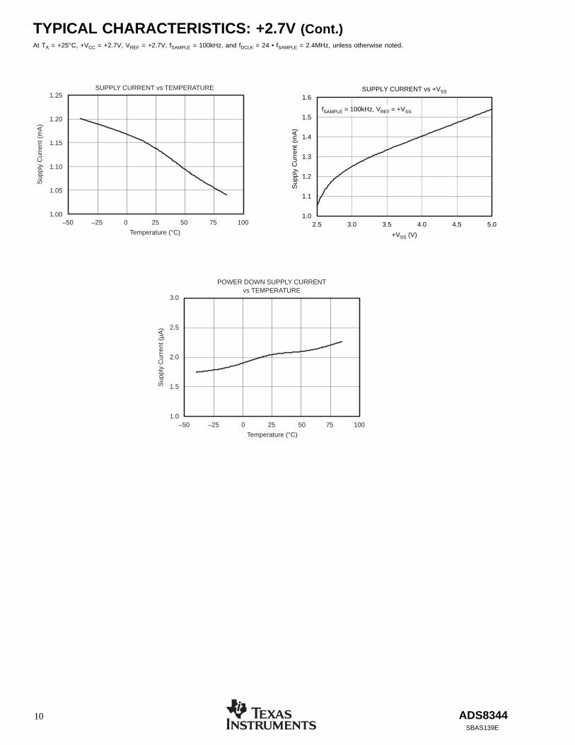
TYPICAL CHARACTERISTICS: +2.7V (Cont.)At TA = +25°C, +VCC = +2.7V, VREF = +2.7V, fSAMPLE = 100kHz, and fDCLK = 24 • fSAMPLE = 2.4MHz, unless otherwise noted.
1.25
1.20
1.15
1.10
1.05
1.00–50 –25 0 25 50 75 100
SUPPLY CURRENT vs TEMPERATURE
Temperature (°C)
Sup
ply
Cur
rent
(m
A)
SUPPLY CURRENT vs +VSS
2.5 3.0 3.5 4.0 4.5 5.0
+VSS (V)
Sup
ply
Cur
rent
(m
A)
1.6
1.5
1.4
1.3
1.2
1.1
1.0
fSAMPLE = 100kHz, VREF = +VSS
POWER DOWN SUPPLY CURRENTvs TEMPERATURE
3.0
2.5
2.0
1.5
1.0
Sup
ply
Cur
rent
(µA
)
Temperature (°C)
–50 –25 0 25 50 75 100
ADS8344 11SBAS139E
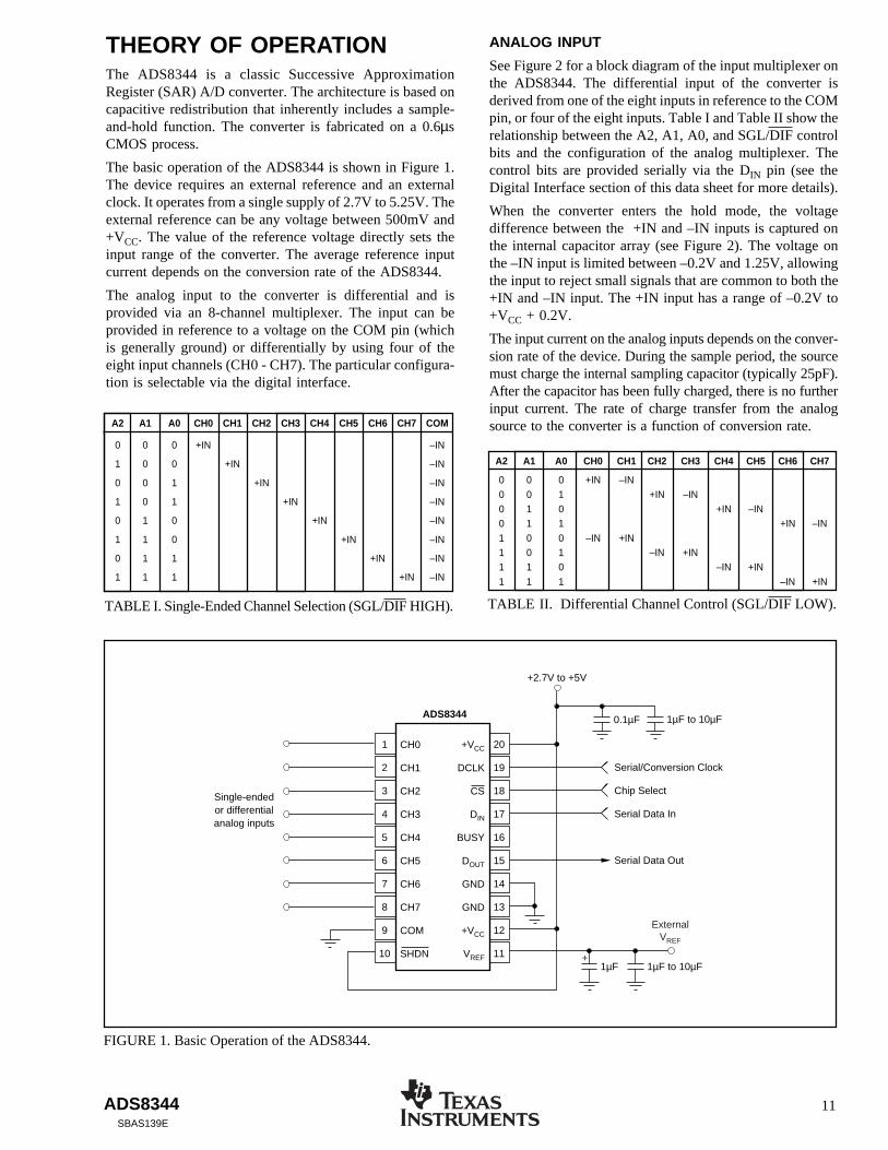
THEORY OF OPERATIONThe ADS8344 is a classic Successive ApproximationRegister (SAR) A/D converter. The architecture is based oncapacitive redistribution that inherently includes a sample-and-hold function. The converter is fabricated on a 0.6µsCMOS process.
The basic operation of the ADS8344 is shown in Figure 1.The device requires an external reference and an externalclock. It operates from a single supply of 2.7V to 5.25V. Theexternal reference can be any voltage between 500mV and+VCC. The value of the reference voltage directly sets theinput range of the converter. The average reference inputcurrent depends on the conversion rate of the ADS8344.
The analog input to the converter is differential and isprovided via an 8-channel multiplexer. The input can beprovided in reference to a voltage on the COM pin (whichis generally ground) or differentially by using four of theeight input channels (CH0 - CH7). The particular configura-tion is selectable via the digital interface.
A2 A1 A0 CH0 CH1 CH2 CH3 CH4 CH5 CH6 CH7
0 0 0 +IN –IN0 0 1 +IN –IN0 1 0 +IN –IN0 1 1 +IN –IN1 0 0 –IN +IN1 0 1 –IN +IN1 1 0 –IN +IN1 1 1 –IN +IN
TABLE II. Differential Channel Control (SGL/DIF LOW).TABLE I. Single-Ended Channel Selection (SGL/DIF HIGH).
FIGURE 1. Basic Operation of the ADS8344.
A2 A1 A0 CH0 CH1 CH2 CH3 CH4 CH5 CH6 CH7 COM
0 0 0 +IN –IN
1 0 0 +IN –IN
0 0 1 +IN –IN
1 0 1 +IN –IN
0 1 0 +IN –IN
1 1 0 +IN –IN
0 1 1 +IN –IN
1 1 1 +IN –IN
ANALOG INPUT
See Figure 2 for a block diagram of the input multiplexer onthe ADS8344. The differential input of the converter isderived from one of the eight inputs in reference to the COMpin, or four of the eight inputs. Table I and Table II show therelationship between the A2, A1, A0, and SGL/DIF controlbits and the configuration of the analog multiplexer. Thecontrol bits are provided serially via the DIN pin (see theDigital Interface section of this data sheet for more details).
When the converter enters the hold mode, the voltagedifference between the +IN and –IN inputs is captured onthe internal capacitor array (see Figure 2). The voltage onthe –IN input is limited between –0.2V and 1.25V, allowingthe input to reject small signals that are common to both the+IN and –IN input. The +IN input has a range of –0.2V to+VCC + 0.2V.
The input current on the analog inputs depends on the conver-sion rate of the device. During the sample period, the sourcemust charge the internal sampling capacitor (typically 25pF).After the capacitor has been fully charged, there is no furtherinput current. The rate of charge transfer from the analogsource to the converter is a function of conversion rate.
CH0
CH1
CH2
CH3
CH4
CH5
CH6
CH7
COM
SHDN
1
2
3
4
5
6
7
8
9
10
20
19
18
17
16
15
14
13
12
11
+VCC
DCLK
CS
DIN
BUSY
DOUT
GND
GND
+VCC
VREF
Serial/Conversion Clock
Chip Select
Serial Data In
Serial Data Out
+2.7V to +5V
1µF to 10µFADS8344
Single-endedor differentialanalog inputs
1µF to 10µF1µF
0.1µF
+
ExternalVREF
ADS834412SBAS139E
REFERENCE INPUT
The external reference sets the analog input range. TheADS8344 will operate with a reference in the range of100mV to +VCC. Keep in mind that the analog input is thedifference between the +IN input and the –IN input, asshown in Figure 2. For example, in the single-ended mode,a 1.25V reference with the COM pin grounded, the selectedinput channel (CH0 - CH7) will properly digitize a signal inthe range of 0V to 1.25V. If the COM pin is connected to0.5V, the input range on the selected channel is 0.5V to1.75V.
There are several critical items concerning the referenceinput and its wide-voltage range. As the reference voltage isreduced, the analog voltage weight of each digital outputcode is also reduced. This is often referred to as the LSB
FIGURE 2. Simplified Diagram of the Analog Input.
Converter+IN
–IN
CH0
CH1
CH2
CH3
A2-A0(shown 00oB)(1)
SGL/DIF(shown HIGH)
CH4
CH5
CH6
CH7
COM
NOTE: (1) See Truth Tables, Table Iand Table II for address coding.
(Least Significant Bit) size and is equal to the referencevoltage divided by 65536. Any offset or gain error inherentin the A/D converter will appear to increase, in terms of LSBsize, as the reference voltage is reduced. For example, if theoffset of a given converter is 2LSBs with a 2.5V reference,then it will typically be 10LSBs with a 0.5V reference. Ineach case, the actual offset of the device is the same,76.3µV.
Likewise, the noise or uncertainty of the digitized outputwill increase with lower LSB size. With a reference voltageof 500mV, the LSB size is 7.6µV. This level is below theinternal noise of the device. As a result, the digital outputcode will not be stable and will vary around a mean value bya number of LSBs. The distribution of output codes will begaussian and the noise can be reduced by simply averagingconsecutive conversion results or applying a digital filter.
With a lower reference voltage, care should be taken toprovide a clean layout including adequate bypassing, a clean(low-noise, low-ripple) power supply, a low-noise reference,and a low-noise input signal. Because the LSB size is lower,the converter will also be more sensitive to nearby digitalsignals and electromagnetic interference.
The voltage into the VREF input is not buffered and directlydrives the Capacitor Digital-to-Analog Converter (CDAC)portion of the ADS8344. Typically, the input current is13µA with a 2.5V reference. This value will vary bymicroamps depending on the result of the conversion. Thereference current diminishes directly with both conversionrate and reference voltage. As the current from the referenceis drawn on each bit decision, clocking the converter morequickly during a given conversion period will not reduceoverall current drain from the reference.
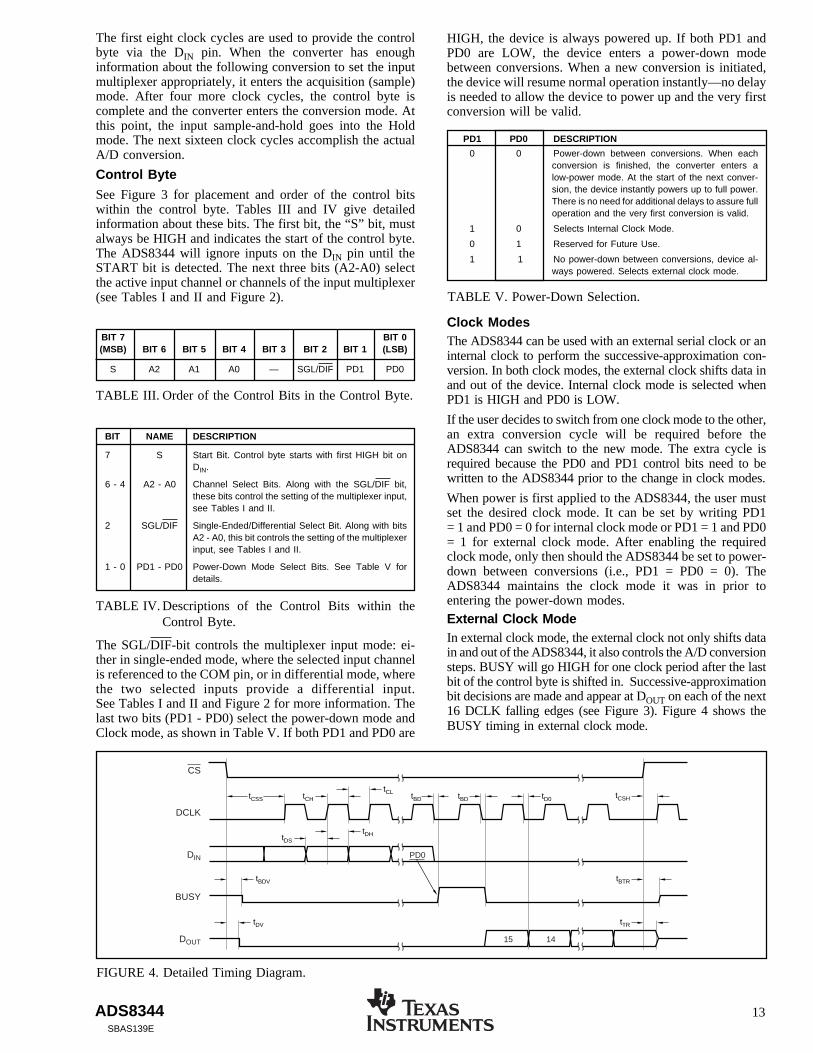
DIGITAL INTERFACE
The ADS8344 has a four-wire serial interface compatiblewith several microprocessor families (note that the digitalinputs are over-voltage tolerant up to +5.5V, regardless of+VCC). Figure 3 shows the typical operation of the ADS8344digital interface.
Most microprocessors communicate using 8-bit transfers;the ADS8344 can complete a conversion with three suchtransfers, for a total of 24 clock cycles on the DCLK input,provided the timing is as shown in Figure 3.
FIGURE 3. Conversion Timing, 24-Clocks per Conversion, 8-Bit Bus Interface. No DCLK Delay Required with DedicatedSerial Port.
tACQ
AcquireIdle Conversion
1DCLK
CS
8 1
15 DOUT
BUSY
(MSB)
(START)
(LSB)
A2SDIN A1 A0 SGL/DIF PD1 PD0
14 13 12 11 10 9 8 7 6 5 4 3 2 1 0 Zero Filled...
8 1 8
AcquireIdle Conversion
1 8 1
15
(MSB)
(START)
A2S A1 A0 SGL/DIF PD1 PD0
14
ADS8344 13SBAS139E
The first eight clock cycles are used to provide the controlbyte via the DIN pin. When the converter has enoughinformation about the following conversion to set the inputmultiplexer appropriately, it enters the acquisition (sample)mode. After four more clock cycles, the control byte iscomplete and the converter enters the conversion mode. Atthis point, the input sample-and-hold goes into the Holdmode. The next sixteen clock cycles accomplish the actualA/D conversion.
Control Byte
See Figure 3 for placement and order of the control bitswithin the control byte. Tables III and IV give detailedinformation about these bits. The first bit, the “S” bit, mustalways be HIGH and indicates the start of the control byte.The ADS8344 will ignore inputs on the DIN pin until theSTART bit is detected. The next three bits (A2-A0) selectthe active input channel or channels of the input multiplexer(see Tables I and II and Figure 2).
BIT 7 BIT 0(MSB) BIT 6 BIT 5 BIT 4 BIT 3 BIT 2 BIT 1 (LSB)
S A2 A1 A0 — SGL/DIF PD1 PD0
TABLE III. Order of the Control Bits in the Control Byte.
TABLE IV. Descriptions of the Control Bits within theControl Byte.
BIT NAME DESCRIPTION
7 S Start Bit. Control byte starts with first HIGH bit onDIN.
6 - 4 A2 - A0 Channel Select Bits. Along with the SGL/DIF bit,these bits control the setting of the multiplexer input,see Tables I and II.
2 SGL/DIF Single-Ended/Differential Select Bit. Along with bitsA2 - A0, this bit controls the setting of the multiplexerinput, see Tables I and II.
1 - 0 PD1 - PD0 Power-Down Mode Select Bits. See Table V fordetails.
PD1 PD0 DESCRIPTION
0 0 Power-down between conversions. When eachconversion is finished, the converter enters alow-power mode. At the start of the next conver-sion, the device instantly powers up to full power.There is no need for additional delays to assure fulloperation and the very first conversion is valid.
1 0 Selects Internal Clock Mode.
0 1 Reserved for Future Use.
1 1 No power-down between conversions, device al-ways powered. Selects external clock mode.
TABLE V. Power-Down Selection.
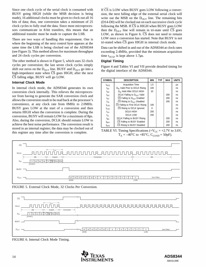
FIGURE 4. Detailed Timing Diagram.
PD0
tBDV
tDH
tCH
tCL
tDS
tCSS
tDV
tBD tBD
tTR
tBTR
tD0 tCSH
DCLK
CS
15DOUT
BUSY
DIN
14
HIGH, the device is always powered up. If both PD1 andPD0 are LOW, the device enters a power-down modebetween conversions. When a new conversion is initiated,the device will resume normal operation instantly—no delayis needed to allow the device to power up and the very firstconversion will be valid.
Clock ModesThe ADS8344 can be used with an external serial clock or aninternal clock to perform the successive-approximation con-version. In both clock modes, the external clock shifts data inand out of the device. Internal clock mode is selected whenPD1 is HIGH and PD0 is LOW.
If the user decides to switch from one clock mode to the other,an extra conversion cycle will be required before theADS8344 can switch to the new mode. The extra cycle isrequired because the PD0 and PD1 control bits need to bewritten to the ADS8344 prior to the change in clock modes.
When power is first applied to the ADS8344, the user mustset the desired clock mode. It can be set by writing PD1= 1 and PD0 = 0 for internal clock mode or PD1 = 1 and PD0= 1 for external clock mode. After enabling the requiredclock mode, only then should the ADS8344 be set to power-down between conversions (i.e., PD1 = PD0 = 0). TheADS8344 maintains the clock mode it was in prior toentering the power-down modes.
External Clock ModeIn external clock mode, the external clock not only shifts datain and out of the ADS8344, it also controls the A/D conversionsteps. BUSY will go HIGH for one clock period after the lastbit of the control byte is shifted in. Successive-approximationbit decisions are made and appear at DOUT on each of the next16 DCLK falling edges (see Figure 3). Figure 4 shows theBUSY timing in external clock mode.
The SGL/DIF-bit controls the multiplexer input mode: ei-ther in single-ended mode, where the selected input channelis referenced to the COM pin, or in differential mode, wherethe two selected inputs provide a differential input.See Tables I and II and Figure 2 for more information. Thelast two bits (PD1 - PD0) select the power-down mode andClock mode, as shown in Table V. If both PD1 and PD0 are
ADS834414SBAS139E
SYMBOL DESCRIPTION MIN TYP MAX UNITS
tACQ Acquisition Time 1.5 µstDS DIN Valid Prior to DCLK Rising 100 nstDH DIN Hold After DCLK HIGH 10 nstDO DCLK Falling to DOUT Valid 200 nstDV CS Falling to DOUT Enabled 200 nstTR CS Rising to DOUT Disabled 200 nstCSS CS Falling to First DCLK Rising 100 nstCSH CS Rising to DCLK Ignored 0 nstCH DCLK HIGH 200 nstCL DCLK LOW 200 nstBD DCLK Falling to BUSY Rising 200 nstBDV CS Falling to BUSY Enabled 200 nstBTR CS Rising to BUSY Disabled 200 ns
TABLE VI. Timing Specifications (+VCC = +2.7V to 3.6V,TA = –40°C to +85°C, CLOAD = 50pF).
Since one clock cycle of the serial clock is consumed withBUSY going HIGH (while the MSB decision is beingmade), 16 additional clocks must be given to clock out all 16bits of data; thus, one conversion takes a minimum of 25clock cycles to fully read the data. Since most microproces-sors communicate in 8-bit transfers, this means that anadditional transfer must be made to capture the LSB.
There are two ways of handling this requirement. One iswhere the beginning of the next control byte appears at thesame time the LSB is being clocked out of the ADS8344(see Figure 3). This method allows for maximum throughputand 24 clock cycles per conversion.
The other method is shown in Figure 5, which uses 32 clockcycles per conversion; the last seven clock cycles simplyshift out zeros on the DOUT line. BUSY and DOUT go into ahigh-impedance state when CS goes HIGH; after the nextCS falling edge, BUSY will go LOW.
Internal Clock Mode
In internal clock mode, the ADS8344 generates its ownconversion clock internally. This relieves the microproces-sor from having to generate the SAR conversion clock andallows the conversion result to be read back at the processor’sconvenience, at any clock rate from 0MHz to 2.0MHz.BUSY goes LOW at the start of a conversion and thenreturns HIGH when the conversion is complete. During theconversion, BUSY will remain LOW for a maximum of 8µs.Also, during the conversion, DCLK should remain LOW toachieve the best noise performance. The conversion result isstored in an internal register; the data may be clocked out ofthis register any time after the conversion is complete.
tACQ
AcquireIdle Conversion
1DCLK
CS
8 1
15 DOUT
BUSY
(MSB)
(START)
(LSB)
A2SDIN A1 A0 SGL/DIF PD1 PD0
14 13 12 11 10 9 8 7 6 5 4 3 2 1 0
8 1 8
Idle
1 8
Zero Filled...
If CS is LOW when BUSY goes LOW following a conver-sion, the next falling edge of the external serial clock willwrite out the MSB on the DOUT line. The remaining bits(D14-D0) will be clocked out on each successive clock cyclefollowing the MSB. If CS is HIGH when BUSY goes LOWthen the DOUT line will remain in tri-state until CS goesLOW, as shown in Figure 6. CS does not need to remainLOW once a conversion has started. Note that BUSY is nottri-stated when CS goes HIGH in internal clock mode.
Data can be shifted in and out of the ADS8344 at clock ratesexceeding 2.4MHz, provided that the minimum acquisitiontime tACQ, is kept above 1.7µs.
Digital Timing
Figure 4 and Tables VI and VII provide detailed timing forthe digital interface of the ADS8344.
tACQ
AcquireIdle Conversion
1DCLK
CS
8 9 10 11 12 13 14 15 16 17 18 19 20 21 22 23 24 25 26 27 28 29 30 31 32
15 DOUT
BUSY
(MSB)
(START)
(LSB)
A2SDIN A1 A0 SGL/DIF PD1 PD0
14 13 12 11 10 9 8 7 6 5 4 3 2 1 0 Zero Filled...
FIGURE 5. External Clock Mode, 32 Clocks Per Conversion.
FIGURE 6. Internal Clock Mode Timing.
ADS8344 15SBAS139E
SYMBOL DESCRIPTION MIN TYP MAX UNITS
tACQ Acquisition Time 1.7 µstDS DIN Valid Prior to DCLK Rising 50 nstDH DIN Hold After DCLK HIGH 10 nstDO DCLK Falling to DOUT Valid 100 nstDV CS Falling to DOUT Enabled 70 nstTR CS Rising to DOUT Disabled 70 nstCSS CS Falling to First DCLK Rising 50 nstCSH CS Rising to DCLK Ignored 0 nstCH DCLK HIGH 150 nstCL DCLK LOW 150 nstBD DCLK Falling to BUSY Rising 100 nstBDV CS Falling to BUSY Enabled 70 nstBTR CS Rising to BUSY Disabled 70 ns
FIGURE 7. Ideal Input Voltages and Output Codes.
TABLE VII. Timing Specifications (+VCC = +4.75V to+5.25V, TA = –40°C to +85°C, CLOAD = 50pF).
Out
put C
ode
0V
FS = Full-Scale Voltage = VREF1LSB = VREF/65,536
FS – 1LSB
11...111
11...110
11...101
00...010
00...001
00...000
1LSB
NOTE: (1) Voltage at converter input, after multiplexer: +IN – (–IN). (See Figure 2.)
Input Voltage(1) (V)
Data Format
The ADS8344 output data is in straight binary format, asshown in Figure 7. This figure shows the ideal output codefor the given input voltage and does not include the effectsof offset, gain, or noise.
POWER DISSIPATION
There are three power modes for the ADS8344: full-power(PD1 - PD0 = 11B), auto power-down (PD1 - PD0 = 00B),and shutdown (SHDN LOW). The effects of these modesvaries depending on how the ADS8344 is being operated.For example, at full conversion rate and 24-clocks perconversion, there is very little difference betweenfull-power mode and auto power-down; a shutdown will notlower power dissipation.
When operating at full-speed and 24-clocks per conversion(see Figure 3), the ADS8344 spends most of its timeacquiring or converting. There is little time for autopower-down, assuming that this mode is active. Thus, thedifference between full-power mode and auto power-downis negligible. If the conversion rate is decreased by simplyslowing the frequency of the DCLK input, the two modes
remain approximately equal. However, if the DCLK fre-quency is kept at the maximum rate during a conversion, butconversions are simply done less often, then the differencebetween the two modes is dramatic. In the latter case, theconverter spends an increasing percentage of its time inpower-down mode (assuming the auto power-down mode isactive).
If DCLK is active and CS is LOW while the ADS8344 is inauto power-down mode, the device will continue to dissipatesome power in the digital logic. The power can be reducedto a minimum by keeping CS HIGH.
Operating the ADS8344 in auto power-down mode willresult in the lowest power dissipation, and there is noconversion time “penalty” on power-up. The very firstconversion will be valid. SHDN can be used to force animmediate power-down.
NOISE
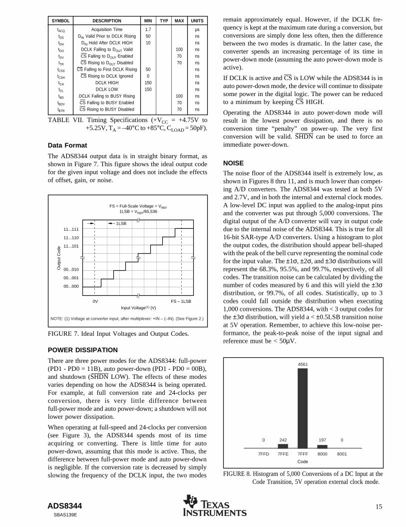
The noise floor of the ADS8344 itself is extremely low, asshown in Figures 8 thru 11, and is much lower than compet-ing A/D converters. The ADS8344 was tested at both 5Vand 2.7V, and in both the internal and external clock modes.A low-level DC input was applied to the analog-input pinsand the converter was put through 5,000 conversions. Thedigital output of the A/D converter will vary in output codedue to the internal noise of the ADS8344. This is true for all16-bit SAR-type A/D converters. Using a histogram to plotthe output codes, the distribution should appear bell-shapedwith the peak of the bell curve representing the nominal codefor the input value. The ±1σ, ±2σ, and ±3σ distributions willrepresent the 68.3%, 95.5%, and 99.7%, respectively, of allcodes. The transition noise can be calculated by dividing thenumber of codes measured by 6 and this will yield the ±3σdistribution, or 99.7%, of all codes. Statistically, up to 3codes could fall outside the distribution when executing1,000 conversions. The ADS8344, with < 3 output codes forthe ±3σ distribution, will yield a < ±0.5LSB transition noiseat 5V operation. Remember, to achieve this low-noise per-formance, the peak-to-peak noise of the input signal andreference must be < 50µV.
FIGURE 8. Histogram of 5,000 Conversions of a DC Input at theCode Transition, 5V operation external clock mode.
Code
4561
2420 0197
7FFE7FFD 800180007FFF
ADS834416SBAS139E
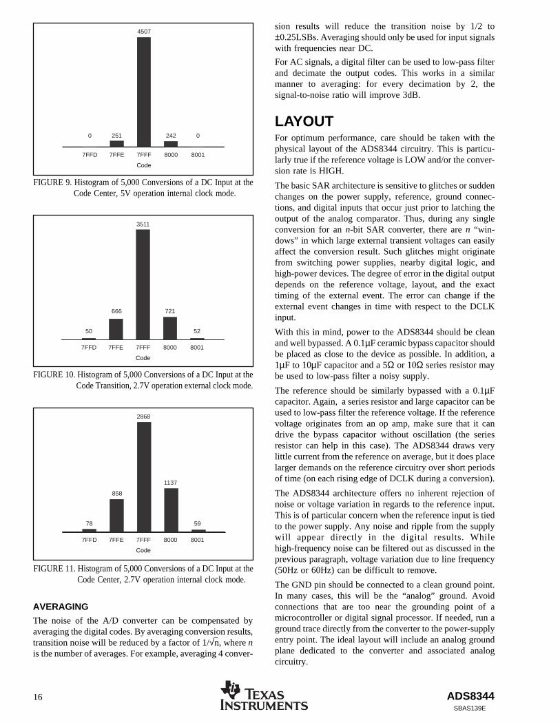
FIGURE 9. Histogram of 5,000 Conversions of a DC Input at theCode Center, 5V operation internal clock mode.
Code
4507
2510 0242
7FFE7FFD 800180007FFF
FIGURE 10. Histogram of 5,000 Conversions of a DC Input at theCode Transition, 2.7V operation external clock mode.
FIGURE 11. Histogram of 5,000 Conversions of a DC Input at theCode Center, 2.7V operation internal clock mode.
Code
3511
721666
50 52
7FFE7FFD 800180007FFF
Code
2868
1137
858
78 59
7FFE7FFD 800180007FFF
sion results will reduce the transition noise by 1/2 to±0.25LSBs. Averaging should only be used for input signalswith frequencies near DC.
For AC signals, a digital filter can be used to low-pass filterand decimate the output codes. This works in a similarmanner to averaging: for every decimation by 2, thesignal-to-noise ratio will improve 3dB.
LAYOUTFor optimum performance, care should be taken with thephysical layout of the ADS8344 circuitry. This is particu-larly true if the reference voltage is LOW and/or the conver-sion rate is HIGH.
The basic SAR architecture is sensitive to glitches or suddenchanges on the power supply, reference, ground connec-tions, and digital inputs that occur just prior to latching theoutput of the analog comparator. Thus, during any singleconversion for an n-bit SAR converter, there are n “win-dows” in which large external transient voltages can easilyaffect the conversion result. Such glitches might originatefrom switching power supplies, nearby digital logic, andhigh-power devices. The degree of error in the digital outputdepends on the reference voltage, layout, and the exacttiming of the external event. The error can change if theexternal event changes in time with respect to the DCLKinput.
With this in mind, power to the ADS8344 should be cleanand well bypassed. A 0.1µF ceramic bypass capacitor shouldbe placed as close to the device as possible. In addition, a1µF to 10µF capacitor and a 5Ω or 10Ω series resistor maybe used to low-pass filter a noisy supply.
The reference should be similarly bypassed with a 0.1µFcapacitor. Again, a series resistor and large capacitor can beused to low-pass filter the reference voltage. If the referencevoltage originates from an op amp, make sure that it candrive the bypass capacitor without oscillation (the seriesresistor can help in this case). The ADS8344 draws verylittle current from the reference on average, but it does placelarger demands on the reference circuitry over short periodsof time (on each rising edge of DCLK during a conversion).
The ADS8344 architecture offers no inherent rejection ofnoise or voltage variation in regards to the reference input.This is of particular concern when the reference input is tiedto the power supply. Any noise and ripple from the supplywill appear directly in the digital results. Whilehigh-frequency noise can be filtered out as discussed in theprevious paragraph, voltage variation due to line frequency(50Hz or 60Hz) can be difficult to remove.
The GND pin should be connected to a clean ground point.In many cases, this will be the “analog” ground. Avoidconnections that are too near the grounding point of amicrocontroller or digital signal processor. If needed, run aground trace directly from the converter to the power-supplyentry point. The ideal layout will include an analog groundplane dedicated to the converter and associated analogcircuitry.
AVERAGING
The noise of the A/D converter can be compensated byaveraging the digital codes. By averaging conversion results,transition noise will be reduced by a factor of 1/√n, where nis the number of averages. For example, averaging 4 conver-
ADS8344 17SBAS139E
DATE REVISION PAGE SECTION DESCRIPTION
2 Package/Ordering Info Added quantity to last column.
4 Electrical Characteristics Fixed typo. Changed +2.7V Gain Error minimum value (for EB, NB grade)from ±0.0024 to ±0.024.
Revision History
NOTE: Page numbers for previous revisions may differ from page numbers in the current version.
9/06 E
PACKAGE OPTION ADDENDUM
www.ti.com 8-Nov-2014
Addendum-Page 1
PACKAGING INFORMATION
Orderable Device Status(1)
Package Type PackageDrawing
Pins PackageQty
Eco Plan(2)
Lead/Ball Finish(6)
MSL Peak Temp(3)
Op Temp (°C) Device Marking(4/5)
Samples
ADS8344E ACTIVE SSOP DBQ 20 50 Green (RoHS& no Sb/Br)
CU NIPDAU Level-2-260C-1 YEAR -40 to 85 ADS8344E
ADS8344E/2K5 ACTIVE SSOP DBQ 20 2500 Green (RoHS& no Sb/Br)
CU NIPDAU Level-3-260C-168 HR -40 to 85 ADS8344E
ADS8344E/2K5G4 ACTIVE SSOP DBQ 20 2500 Green (RoHS& no Sb/Br)
CU NIPDAU Level-3-260C-168 HR -40 to 85 ADS8344E
ADS8344EB ACTIVE SSOP DBQ 20 50 Green (RoHS& no Sb/Br)
CU NIPDAU Level-3-260C-168 HR -40 to 85 ADS8344EB
ADS8344EB/2K5 ACTIVE SSOP DBQ 20 2500 Green (RoHS& no Sb/Br)
CU NIPDAU Level-3-260C-168 HR -40 to 85 ADS8344EB
ADS8344EB/2K5G4 ACTIVE SSOP DBQ 20 2500 Green (RoHS& no Sb/Br)
CU NIPDAU Level-3-260C-168 HR -40 to 85 ADS8344EB
ADS8344EBG4 ACTIVE SSOP DBQ 20 50 Green (RoHS& no Sb/Br)
CU NIPDAU Level-3-260C-168 HR -40 to 85 ADS8344EB
ADS8344EG4 ACTIVE SSOP DBQ 20 50 Green (RoHS& no Sb/Br)
CU NIPDAU Level-2-260C-1 YEAR -40 to 85 ADS8344E
ADS8344N ACTIVE SSOP DB 20 70 Green (RoHS& no Sb/Br)
CU NIPDAU Level-2-260C-1 YEAR -40 to 85 ADS8344NB
ADS8344N/1K ACTIVE SSOP DB 20 1000 Green (RoHS& no Sb/Br)
CU NIPDAU Level-2-260C-1 YEAR -40 to 85 ADS8344NB
ADS8344N/1KG4 ACTIVE SSOP DB 20 1000 Green (RoHS& no Sb/Br)
CU NIPDAU Level-2-260C-1 YEAR -40 to 85 ADS8344NB
ADS8344NB ACTIVE SSOP DB 20 70 Green (RoHS& no Sb/Br)
CU NIPDAU Level-2-260C-1 YEAR -40 to 85 ADS8344NB
ADS8344NB/1K ACTIVE SSOP DB 20 1000 Green (RoHS& no Sb/Br)
CU NIPDAU Level-2-260C-1 YEAR -40 to 85 ADS8344NB
ADS8344NB/1KG4 ACTIVE SSOP DB 20 1000 Green (RoHS& no Sb/Br)
CU NIPDAU Level-2-260C-1 YEAR -40 to 85 ADS8344NB
ADS8344NBG4 ACTIVE SSOP DB 20 70 Green (RoHS& no Sb/Br)
CU NIPDAU Level-2-260C-1 YEAR -40 to 85 ADS8344NB
ADS8344NG4 ACTIVE SSOP DB 20 70 Green (RoHS& no Sb/Br)
CU NIPDAU Level-2-260C-1 YEAR -40 to 85 ADS8344NB
(1) The marketing status values are defined as follows:ACTIVE: Product device recommended for new designs.
PACKAGE OPTION ADDENDUM
www.ti.com 8-Nov-2014
Addendum-Page 2
LIFEBUY: TI has announced that the device will be discontinued, and a lifetime-buy period is in effect.NRND: Not recommended for new designs. Device is in production to support existing customers, but TI does not recommend using this part in a new design.PREVIEW: Device has been announced but is not in production. Samples may or may not be available.OBSOLETE: TI has discontinued the production of the device.
(2) Eco Plan - The planned eco-friendly classification: Pb-Free (RoHS), Pb-Free (RoHS Exempt), or Green (RoHS & no Sb/Br) - please check http://www.ti.com/productcontent for the latest availabilityinformation and additional product content details.TBD: The Pb-Free/Green conversion plan has not been defined.Pb-Free (RoHS): TI's terms "Lead-Free" or "Pb-Free" mean semiconductor products that are compatible with the current RoHS requirements for all 6 substances, including the requirement thatlead not exceed 0.1% by weight in homogeneous materials. Where designed to be soldered at high temperatures, TI Pb-Free products are suitable for use in specified lead-free processes.Pb-Free (RoHS Exempt): This component has a RoHS exemption for either 1) lead-based flip-chip solder bumps used between the die and package, or 2) lead-based die adhesive used betweenthe die and leadframe. The component is otherwise considered Pb-Free (RoHS compatible) as defined above.Green (RoHS & no Sb/Br): TI defines "Green" to mean Pb-Free (RoHS compatible), and free of Bromine (Br) and Antimony (Sb) based flame retardants (Br or Sb do not exceed 0.1% by weightin homogeneous material)
(3) MSL, Peak Temp. - The Moisture Sensitivity Level rating according to the JEDEC industry standard classifications, and peak solder temperature.
(4) There may be additional marking, which relates to the logo, the lot trace code information, or the environmental category on the device.
(5) Multiple Device Markings will be inside parentheses. Only one Device Marking contained in parentheses and separated by a "~" will appear on a device. If a line is indented then it is a continuationof the previous line and the two combined represent the entire Device Marking for that device.
(6) Lead/Ball Finish - Orderable Devices may have multiple material finish options. Finish options are separated by a vertical ruled line. Lead/Ball Finish values may wrap to two lines if the finishvalue exceeds the maximum column width.
Important Information and Disclaimer:The information provided on this page represents TI's knowledge and belief as of the date that it is provided. TI bases its knowledge and belief on informationprovided by third parties, and makes no representation or warranty as to the accuracy of such information. Efforts are underway to better integrate information from third parties. TI has taken andcontinues to take reasonable steps to provide representative and accurate information but may not have conducted destructive testing or chemical analysis on incoming materials and chemicals.TI and TI suppliers consider certain information to be proprietary, and thus CAS numbers and other limited information may not be available for release.
In no event shall TI's liability arising out of such information exceed the total purchase price of the TI part(s) at issue in this document sold by TI to Customer on an annual basis.
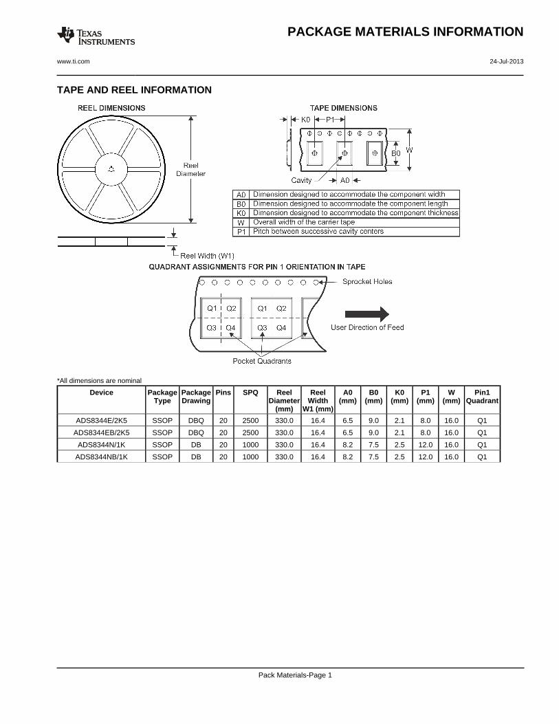
TAPE AND REEL INFORMATION
*All dimensions are nominal
Device PackageType
PackageDrawing
Pins SPQ ReelDiameter
(mm)
ReelWidth
W1 (mm)
A0(mm)
B0(mm)
K0(mm)
P1(mm)
W(mm)
Pin1Quadrant
ADS8344E/2K5 SSOP DBQ 20 2500 330.0 16.4 6.5 9.0 2.1 8.0 16.0 Q1
ADS8344EB/2K5 SSOP DBQ 20 2500 330.0 16.4 6.5 9.0 2.1 8.0 16.0 Q1
ADS8344N/1K SSOP DB 20 1000 330.0 16.4 8.2 7.5 2.5 12.0 16.0 Q1
ADS8344NB/1K SSOP DB 20 1000 330.0 16.4 8.2 7.5 2.5 12.0 16.0 Q1
PACKAGE MATERIALS INFORMATION
www.ti.com 24-Jul-2013
Pack Materials-Page 1
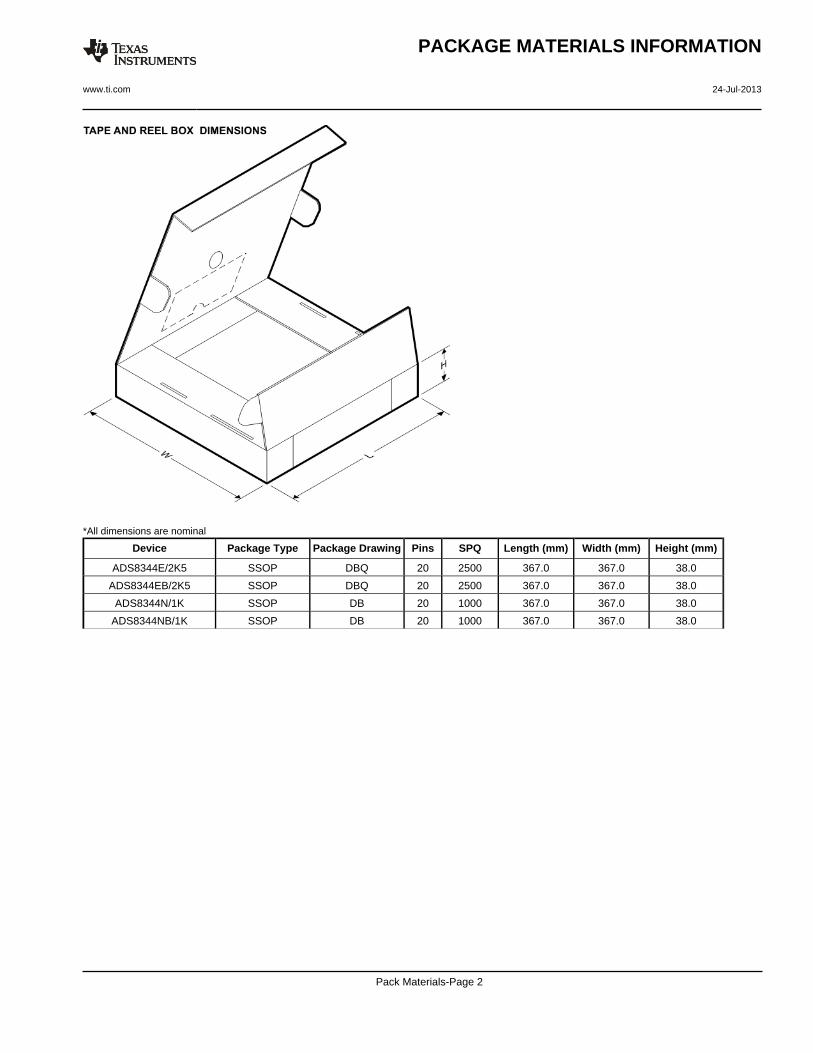
*All dimensions are nominal
Device Package Type Package Drawing Pins SPQ Length (mm) Width (mm) Height (mm)
ADS8344E/2K5 SSOP DBQ 20 2500 367.0 367.0 38.0
ADS8344EB/2K5 SSOP DBQ 20 2500 367.0 367.0 38.0
ADS8344N/1K SSOP DB 20 1000 367.0 367.0 38.0
ADS8344NB/1K SSOP DB 20 1000 367.0 367.0 38.0
PACKAGE MATERIALS INFORMATION
www.ti.com 24-Jul-2013
Pack Materials-Page 2
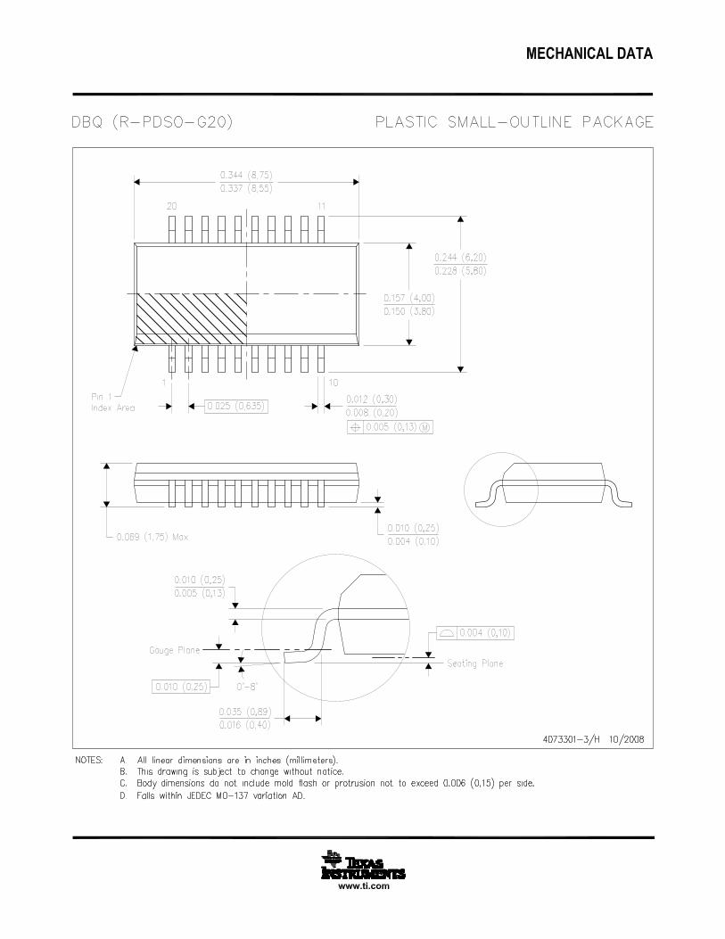
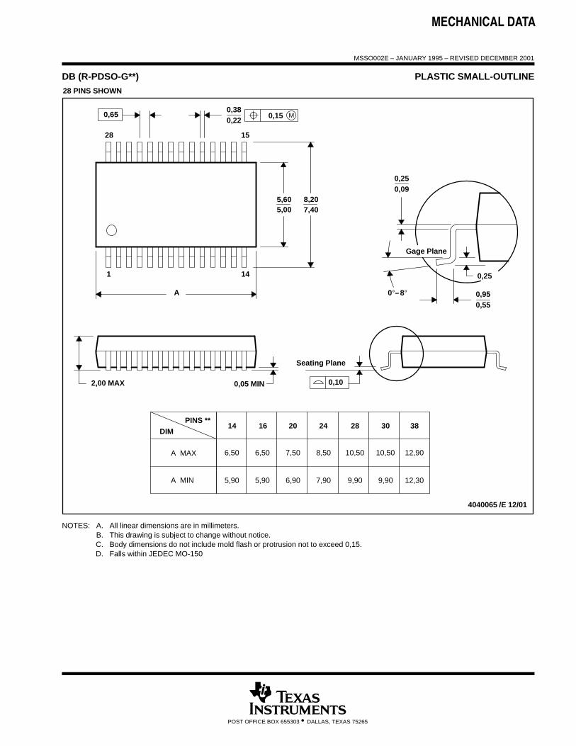
MECHANICAL DATA
MSSO002E – JANUARY 1995 – REVISED DECEMBER 2001
POST OFFICE BOX 655303 • DALLAS, TEXAS 75265
DB (R-PDSO-G**) PLASTIC SMALL-OUTLINE
4040065 /E 12/01
28 PINS SHOWN
Gage Plane
8,207,40
0,550,95
0,25
38
12,90
12,30
28
10,50
24
8,50
Seating Plane
9,907,90
30
10,50
9,90
0,38
5,605,00
15
0,22
14
A
28
1
2016
6,506,50
14
0,05 MIN
5,905,90
DIM
A MAX
A MIN
PINS **
2,00 MAX
6,90
7,50
0,65 M0,15
0°–8°
0,10
0,090,25
NOTES: A. All linear dimensions are in millimeters.B. This drawing is subject to change without notice.C. Body dimensions do not include mold flash or protrusion not to exceed 0,15.D. Falls within JEDEC MO-150
IMPORTANT NOTICETexas Instruments Incorporated and its subsidiaries (TI) reserve the right to make corrections, enhancements, improvements and otherchanges to its semiconductor products and services per JESD46, latest issue, and to discontinue any product or service per JESD48, latestissue. Buyers should obtain the latest relevant information before placing orders and should verify that such information is current andcomplete. All semiconductor products (also referred to herein as “components”) are sold subject to TI’s terms and conditions of salesupplied at the time of order acknowledgment.TI warrants performance of its components to the specifications applicable at the time of sale, in accordance with the warranty in TI’s termsand conditions of sale of semiconductor products. Testing and other quality control techniques are used to the extent TI deems necessaryto support this warranty. Except where mandated by applicable law, testing of all parameters of each component is not necessarilyperformed.TI assumes no liability for applications assistance or the design of Buyers’ products. Buyers are responsible for their products andapplications using TI components. To minimize the risks associated with Buyers’ products and applications, Buyers should provideadequate design and operating safeguards.TI does not warrant or represent that any license, either express or implied, is granted under any patent right, copyright, mask work right, orother intellectual property right relating to any combination, machine, or process in which TI components or services are used. Informationpublished by TI regarding third-party products or services does not constitute a license to use such products or services or a warranty orendorsement thereof. Use of such information may require a license from a third party under the patents or other intellectual property of thethird party, or a license from TI under the patents or other intellectual property of TI.Reproduction of significant portions of TI information in TI data books or data sheets is permissible only if reproduction is without alterationand is accompanied by all associated warranties, conditions, limitations, and notices. TI is not responsible or liable for such altereddocumentation. Information of third parties may be subject to additional restrictions.Resale of TI components or services with statements different from or beyond the parameters stated by TI for that component or servicevoids all express and any implied warranties for the associated TI component or service and is an unfair and deceptive business practice.TI is not responsible or liable for any such statements.Buyer acknowledges and agrees that it is solely responsible for compliance with all legal, regulatory and safety-related requirementsconcerning its products, and any use of TI components in its applications, notwithstanding any applications-related information or supportthat may be provided by TI. Buyer represents and agrees that it has all the necessary expertise to create and implement safeguards whichanticipate dangerous consequences of failures, monitor failures and their consequences, lessen the likelihood of failures that might causeharm and take appropriate remedial actions. Buyer will fully indemnify TI and its representatives against any damages arising out of the useof any TI components in safety-critical applications.In some cases, TI components may be promoted specifically to facilitate safety-related applications. With such components, TI’s goal is tohelp enable customers to design and create their own end-product solutions that meet applicable functional safety standards andrequirements. Nonetheless, such components are subject to these terms.No TI components are authorized for use in FDA Class III (or similar life-critical medical equipment) unless authorized officers of the partieshave executed a special agreement specifically governing such use.Only those TI components which TI has specifically designated as military grade or “enhanced plastic” are designed and intended for use inmilitary/aerospace applications or environments. Buyer acknowledges and agrees that any military or aerospace use of TI componentswhich have not been so designated is solely at the Buyer's risk, and that Buyer is solely responsible for compliance with all legal andregulatory requirements in connection with such use.TI has specifically designated certain components as meeting ISO/TS16949 requirements, mainly for automotive use. In any case of use ofnon-designated products, TI will not be responsible for any failure to meet ISO/TS16949.Products ApplicationsAudio www.ti.com/audio Automotive and Transportation www.ti.com/automotiveAmplifiers amplifier.ti.com Communications and Telecom www.ti.com/communicationsData Converters dataconverter.ti.com Computers and Peripherals www.ti.com/computersDLP® Products www.dlp.com Consumer Electronics www.ti.com/consumer-appsDSP dsp.ti.com Energy and Lighting www.ti.com/energyClocks and Timers www.ti.com/clocks Industrial www.ti.com/industrialInterface interface.ti.com Medical www.ti.com/medicalLogic logic.ti.com Security www.ti.com/securityPower Mgmt power.ti.com Space, Avionics and Defense www.ti.com/space-avionics-defenseMicrocontrollers microcontroller.ti.com Video and Imaging www.ti.com/videoRFID www.ti-rfid.comOMAP Applications Processors www.ti.com/omap TI E2E Community e2e.ti.comWireless Connectivity www.ti.com/wirelessconnectivity
Mailing Address: Texas Instruments, Post Office Box 655303, Dallas, Texas 75265Copyright © 2014, Texas Instruments Incorporated