Embed Size (px)
Citation preview

上海芯圣电子股份有限公司 Shanghai Holychip Electronic Co.,Ltd.
1
z
15W Full-Bridge Power Stage with Voltage/Current
Demodulation for High-Integrated Wireless Power Transmitter
1 Descriptions
The SQ520A is a highly integrated wireless power
transmitter analog front end that contains all of the
analog components required to implement a WPC
compliant transmitter. The SQ520A integrates a full-
bridge power driver with MOSFETs, current sense
amplifier, bootstrap circuit, communication
demodulator, linear regulator and protection circuit.
The SQ520A can work with transmitter controller to
create a high-performance wireless power transmitter
that complies with both the WPC V1.2.4 Extended
Power Profile (EPP) and Baseline Power Profile (BPP).
Once an EPP receiver is detected, the transmitter will
provide with up to 15W of output power. If a BPP
receiver is present, the transmitter will deliver only up to
5W of output power.
The system supports foreign object detection (FOD) by
continuously monitoring the amount of power
transferred and comparing that to the amount of
received power, as reported by the receiver. In order
to do this, the SQ520A measures the input DC current
very accurately using a current sense amplifier. Besides,
the SQ520A also supports input under- voltage lockout
(UVLO), over-current protection (OCP), short-circuit
protection (SCP) and over-temperature protection
(OTP). These protections further enhance the reliability
of the total wireless power transmitter system.
The SQ520A is available in a compact 3 x 3 mm QFN
package.
2 Features
4.0V to 14.0V input voltage range
Support 5V/9V/12V input
Support up to 15W output power
Integrated voltage and current demodulation
Integrated 5V LDO for powering MCU
Integrated four 15mohm power FETs
Integrated FET driver and bootstrap circuit
Integrated accurate current sense for FOD
Support various type of transmitter in WPC V1.2.4
BPP A11/A11a
BPP A6 with single coil or dual coil
EPP MPA2
EPP MPA5/MPA11 with additional DC-DC
UVLO/OCP/SCP/OTP
3mm x 3mm QFN package
3 Applications
WPC Compliant Wireless Power Transmitter
Proprietary Wireless Chargers and Transmitter
Medical and Wearable Applications
4 Device Information
Part Number Package Dimension
SQ520A QFN 19 3mm x 3mm x0.75mm

2
SQ520A DATASHEET
5 Typical Application Circuit
Micro-B/TypeC
IDM
IDMO
EN
DP
AG
ND
C
SP
PG
ND
C
SN
3
SQ520A DATASHEET
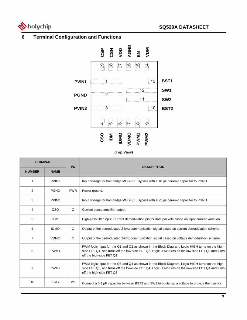
6 Terminal Configuration and Functions
PVIN1
PGND
PVIN2
BST1
SW1
SW2
BST2
(Top View)
TERMINAL
I/O
DESCRIPTION
NUMBER NAME
1 PVIN1 I Input voltage for half-bridge MOSFET. Bypass with a 10 µF ceramic capacitor to PGND.
2 PGND PWR Power ground.
3 PVIN2 I Input voltage for half-bridge MOSFET. Bypass with a 22 µF ceramic capacitor to PGND.
4 CSO O Current sense amplifier output.
5 IDM I High-pass filter input. Current demodulation pin for data packets based on input current variation.
6 IDMO O Output of the demodulated 2-kHz communication signal based on current demodulation scheme.
7 VDMO O Output of the demodulated 2-kHz communication signal based on voltage demodulation scheme.
8
PWM1
I
PWM logic input for the Q1 and Q2 as shown in the Block Diagram. Logic HIGH turns on the high-
side FET Q1, and turns off the low-side FET Q2. Logic LOW turns on the low-side FET Q2 and turns
off the high-side FET Q1
9
PWM2
I
PWM logic input for the Q3 and Q4 as shown in the Block Diagram. Logic HIGH turns on the high-
side FET Q3, and turns off the low-side FET Q4. Logic LOW turns on the low-side FET Q4 and turns
off the high-side FET Q3
10 BST2 I/O
Connect a 0.1 µF capacitor between BST2 and SW2 to bootstrap a voltage to provide the bias for
CS
O
IDM
IDM
O
4
5
6
7
8
9
19
18
17
16
15
14
CS
P
CS
N
VD
D
AG
ND
EN
VD
M
VD
MO
PW
M1
PW
M2

4
SQ520A DATASHEET
high side MOSFET driver.
11 SW2 O Switch node of the half-bridge MOSFET.
12 SW1 O Switch node of the half-bridge MOSFET.
13
BST1
I/O
Connect a 0.1 µF capacitor between BST1 and SW1 to bootstrap a voltage to provide the bias for high
side MOSFET driver.
14 VDM I High-pass filter input. Voltage demodulation pin for data packets based on coil voltage variation.
15 EN I Enable pin. Logic LOW disables the IC. Logic HIGH enables the IC.
16 AGND I/O Analog Ground.
17
VDD
O
Output of internal regulator to provide 5.0V power supply to internal gate drivers and control circuits.
Connect a 2.2 µF ceramic capacitor from VDD to AGND pin.
18 CSN I Negative end of input current sense amplifier.
19 CSP I Positive end of input current sense amplifier.

5
SQ520A DATASHEET
7 Specifications
7.1 Absolute Maximum Ratings
Over operating free-air temperature range (unless otherwise noted) (1)
MIN MAX UNIT
Voltage range at
terminals (2)
PVIN1, PVIN2, SW1, SW2, CSP, CSN -0.3 16 V
PWM1, PWM2, EN, CSO, VDM, IDM, VDMO, IDMO, VDD -0.3 7 V
BST1, BST2 -0.3 21 V
Temperature Range
Operating Junction, TJ -40 150 °C
Storage temperature range, Tstg -65 150 °C
(1) Stresses beyond those listed under absolute maximum ratings may cause permanent damage to the device. These are stress ratings only, and functional operation of the device at these or any other conditions beyond those indicated under recommended operating conditions is not implied. Exposure to absolute-maximum-rated conditions for extended periods may affect device reliability.
(2) All voltage values are with respect to network ground terminal.
7.2 Thermal Information
THERMAL RESISTANCE(1)
QFN-19 (3mm x 3mm) UNIT
ΘJA Junction to ambient thermal resistance 64 °C/W
ΘJC Junction to case resistance 11 °C/W
(1) Measured on JESD51-7, 4-layer PCB.
7.3 Handling Ratings
PARAMETER DEFINITION MIN MAX UNIT
ESD (1)
Human body model (HBM) ESD stress voltage(2)
-8 8 kV
Charged device model (CDM) ESD stress voltage (3)
-1 1 kV
(1) Electrostatic discharge (ESD) to measure device sensitivity and immunity to damage caused by assembly line electrostatic discharges into the device.
(2) Level listed above is the passing level per ANSI, ESDA, and JEDEC JS-001. JEDEC document JEP155 states that 500-V HBM allows safe manufacturing with a standard ESD control process.
(3) Level listed above is the passing level per EIA-JEDEC JESD22-C101. JEDEC document JEP157 states that 250-V CDM allows safe manufacturing with a standard ESD control process.
7.4 Recommended Operating Conditions
MIN TYP MAX UNIT
VPVIN1, VPVIN2 Input voltage range 4
14 V
CPVIN1, CPVIN2 PVIN1, PVIN2 Ceramic Capacitor
10
µF
CBST1, CBST2 BST1-SW1, BST2-SW2 Ceramic Capacitor
0.1
µF
CVDD VDD Ceramic Capacitor
2.2
µF
TJ Operating junction temperature -40
125 C

6
SQ520A DATASHEET
7.5 Electrical Characteristic
TJ= 25°C and VPVIN1 = 5.0V, VPVIN2 = 5.0V, unless otherwise noted.
PARAMETER TEST CONDITIONS MIN TYP MAX UNIT
SUPPLY VOLTAGE
VIN Operating voltage 4 14 V
VIN_UVLO
Under voltage lockout threshold
Rising edge 3.6 V
Falling edge 3.4 V
IQ Quiescent current into VIN EN= high, no switching 0.46 mA
ISD Shutdown current into VIN EN =low 42 μA
VOLTAGE REGULATOR (VDD)
VDD
VDD output voltage
VIN = 5.0V, IVDD =10mA 4.9 V
VIN = 9.0V, IVDD =10mA 5 V
IVDD_LIM VDD current limit VDD = 5.0V 20 mA
CURRENT SENSE AMPLIFIER
G Gain Sense Resistor=20mohm; Sense
Current=2A 49 50 51 V/V
VOO Output offset voltage Measures at the CSO pin; VCSP =
VCSN
0.5 V
POWER SWITCH
RDS(on)
SW1 High-side RDS(on) VDD = 5.0V 15 mΩ
SW1 Low-side RDS(on) VDD = 5.0V 15 mΩ
SW2 High-side RDS(on) VDD = 5.0V 15 mΩ
SW2 Low-side RDS(on) VDD = 5.0V 15 mΩ
SHORT CIRCUIT PROTECTION
ILIM High-side current limit threshold 8 A
Tp Hiccup period 20 ms
EN, PWM1, PWM2
VIH Input logic high 2.4 V
VIL Input logic low 0.4 V
VDMO, IDMO
VOH Output logic high 0.9* VDD V
VOL Input logic low 0.1* VDD V
THERMAL SHUTDOWN
TSD
Thermal shutdown temperature 165 °C
Thermal shutdown hysteresis 15 °C

7
SQ520A DATASHEET
VDD
AMPLIFIER
HD Driver Q1
VDD
LD Driver Q2
VDD
HD Driver Q3
VDD
LD Driver Q4
DEMODULATION
CONTROL
LOGIC
UVLO
VDD
REGULATOR
8 Functional Block Diagram
VDD
CSP
CSN
CSO
PVIN1
BST1
SW1
VDM
IDM PGND
PVIN2
VDMO
IDMO BST2
PWM1
PWM2 SW2
EN
AGND PGND

8
SQ520A DATASHEET
9 Feature Description
9.1 Current Sense Amplifier
To support foreign object detection (FOD), the SQ520A
senses the average input current to the device. The
integrated current sense amplifier has voltage gain of 50.
For proper scaling of the current signal, the recommended
current sense resistor is 10mΩ/20mΩ.
The current sense amplifier output has a typical 0.5V offset
when the sensed current is zero. For accurate
measurement of the input current, MCU need to calibrate
this offset.
9.2 PWM Control
The PWM1 input controls the internal MOSFET Q1 and Q2,
and the PWM2 input controls the internal MOSFET Q3 and
Q4 as shown in the Block Diagram. The PWM1 and PWM2
can independently control the SW1 and SW2 duty cycle
and frequency. Please be noted that dead time has already
been implemented between Q1 (or Q3) and Q2 (or Q4)
internally, so there is no need for dead time between
external control signals PWM1 and PWM2.
9.3 Under-Voltage Lockout (UVLO)
The UVLO function protects the chip from operating at
insufficient power supply. The chip disables all the function
if input voltage is lower than 3.4V (typical) and it doesn’t
start up again until input voltage is higher than 3.6V
(typical).
9.4 Voltage Regulator
The SQ520A has an integrated low-dropout (LDO) voltage
regulator. The internal power drivers and control circuits are
powered from this voltage. The VDD pin supplies a
regulated 5.0V voltage supply. Decouple this pin to power
ground with a 2.2μF low ESR ceramic capacitor placed
close to the IC.
The VDD regulator is enabled once PVIN is above the
UVLO threshold. It is not controlled by the EN signal. The
load capability of VDD regulator is about 20mA, so it can be
used to power up MCU directly.
9.5 Voltage Demodulation
In order to increase the communication reliability in any
load condition, the SQ520A has integrated two
demodulation schemes, one based on input average
current information and the other based on coil voltage
information. The voltage mode envelope detector is
implemented using a discrete solution as depicted on
Figure1. This simple implementation achieves the
envelope detector function low-pass filter as well as the DC
filter function.
Vtank
VDM
VDMO
Fig1. Voltage Demodulation
9.6 Current Demodulation
The current-mode detector takes the modulation
information from the average input current. The capacitor
between CSO and IDM pin can filter the DC current. The
MCU can detect the demodulation results on VDMO and
IDMO pins and then implement the packet decode. The
MCU can select either voltage-mode or current-mode
signals depending upon which produces the best
demodulated signal.
Fig2. Current Demodulation
9.7 Over-Current Protection (OCP)
The SQ520A integrates a hiccup mode over-current
protection. Current of the SW1 high-side FET and SW2
high-side FET are sensed and compared to the current-
limit threshold during every switching cycle. When the
sensed current reaches the current-limit threshold, the
over-current fault counter is incremented. If the over-
current fault counter reaches 8 and overflows, all 4 internal
FETs are turned off regardless of the PWM inputs. The IC
remains in hiccup mode for a period equal to 20ms
typically and then attempts to restart. The hiccup mode
OCP protection can reduce the average current greatly to
alleviate the thermal issue and to protect the converter.
Once the OCP condition is removed, SQ520A exits hiccup
mode and goes back to normal operation.
CSP CSN CSO IDM IDMO
CURRENT
DEMODULATION
VOLTAGE
DEMODULATION

9
SQ520A DATASHEET
9.8 Short-Circuit Protection (SCP)
The SQ520A integrates a latch mode short-circuit
protection. When SW1/2 is shorted to PVIN1/2 or PGND,
the SQ520A will turn off all the 4 internal FETs and latch. To
get out of the latch status, a power on reset (POR) or EN
reset need to be implemented. This protection mode is
especially useful when the adjacent pins are shorted
together due to poor soldering issue and can prevent the
chip from damage.
9.9 Over Temperature Protection (OTP)
The over temperature protection (OTP) prevents the chip
from operating at exceedingly high temperatures. When
the silicon die temperature exceeds 165℃, SQ520A is shut
down. When the temperature drops below threshold
(typically 150℃), the chip is enabled again.

10
SQ520A DATASHEET
10 Application Information
10.1 Input Current Sense
The SQ520A senses the average input current to the device.
The recommended current sense resistor is 10mΩ/20mΩ.
Resistor of 1% or higher accuracy and low temperature
coefficient is recommended.
The resistor power rating and temperature coefficient
should also be considered. The power dissipation is roughly
calculated as P=I2R, and I is the highest current flowing
through the resistor. The resistor power rating should be
higher than the calculated value.
The current sense amplifier output has a typical 0.5V offset
when the sensed current is zero. Please be noted that this
offset may vary a little from one chip to another, so when
MCU is calibrating this offset, it is highly recommended to
use ADC to sense this offset instead of using fixed 0.5V.
Figure 3 shows the internal current sense output (CSO)
voltage over the sensed current based on different sense
resistor. Since the integrated current sense amplifier has
voltage gain of 50V/V, if input current is sensed on a 10mΩ
resistor, the voltage to current gain will be 0.5V/A. If input
current is sensed on a 20mΩ resistor, the voltage to current
gain will be 1V/A.
Fig3. CSO Voltage over Sense Current
10.2 Voltage/Current Demodulation
SQ520A integrates simultaneous voltage and current
demodulation based on coil voltage and input average
current separately. Compared with the discrete
demodulation solution, SQ520A need much less number of
external components.
Figure4 shows a typical circuit for voltage demodulation.
D1/R3/R5/C4 is an envelope demodulation of the LC tank
voltage. R2/C3 is a RC filter which can filter the high
frequency switching noise while keep the 2 kHz
communication signal. C2 is a DC blocking capacitor which
passes through only the ac signal to the internal
demodulator.
Fig4. Voltage Demodulation
Figure5 shows a typical communication packet, which is
comprised of a preamble, a header, the actual message,
and a checksum, as defined by the WPC standard.
Fig5. VDMO/IDMO Demodulation Output
2.0 1.5 1.0
Sense Current [A]
0.5 0.0
0.0
Rsense=20mohm
Rsense=10mohm
0.5
1.0
1.5
2.0
2.5
CS
O [V
]

11
SQ520A DATASHEET
11 Layout Guide
Here are the guidelines to follow:
• Make routing loop as small as possible, especially the power loop, to minimize EMI noises.
• Widen the copper between SW1, SW2 and LC tank, because high current in the LC tank can cause power
losses on the traces and hence low efficiency.
Moreover, the PVIN1/2 routing should be as wide as
possible.
• The input current sense traces should be connected to
the current sense resistor’s pads in Kelvin sense way
as below, and routed in parallel (differential routing). • Place small-size input capacitors as close as possible
between the PVIN1/2 pins and PGND pin. These
capacitors can effectively filter out high-frequency
noises due to their low ESR and ESL. Please refer to
C8 and C11 in Figure 6.
• Separate the analog-ground plane from the power-
ground plane, and use only one point to join them.
Please refer to Figure 7. • Keep analog-ground plane and power-ground plane
low impedance. Use as much copper as possible.
Fig6. Top Layer
Fig7. Bottom Layer

12
SQ520A DATASHEET
12 MECHANICAL DATA
QFN19L (3x3x0.75)